Zero-Voltage Switching and Zero-Current-Switching ... · ZCS or ZVS. However, these circuits to...
10
Zero-Voltage Switching and Zero-Current-Switching Interleaved Boost Converter for reducing Switching Losses * P. Modini 1 , P.Srinivasulu 2 , G. Jayakrishna 3 M.Tech Student, SIETK, Puttur, Chittoor (Dist), Andhra Pradesh, India Associate Professor, Department of EEE, SIETK, Puttur, Chittoor (Dist), Andhra Pradesh, India Professor, Department of EEE, SIETK, Puttur, Chittoor (Dist), Andhra Pradesh, India. Abstract An interleaved boost converter with zero-voltage switching (ZVS) and zero-current switching (ZCS) characteristics is proposed in this project. With this proposed method in addition to decreasing the current stress of the main circuit device, it can able to ripple of the input current and output voltage. In this launching the soft-switching interleaved converter reduces the complexity and cost. To reduce the switching losses main switches can attain the characteristics of ZVS and ZCS consequently. Based on the condition of the duty cycle this converter topology has two operational conditions, to determine these two conditions a driving circuit is proposed. The principle of operation and designed methods of converter is studied and also theoretical analyzed. Simulations results are used to verify the viability and accuracy of the proposed converter. I. Introduction An interleaved boost converter is the combination of two or more number of conventional topologies, and with the same power ratings current through the interleaved boost converter is reduced to half of the conventional topology. The main feature of this interleaved boost converter the input current ripple and output voltage ripple are lower than those of the conventional topologies. The single boost converter can use the zero- voltage switching (ZVS) and/or zero-current switching (ZCS) to minimize the switching loss of the high- frequency switching [1]–[4], [13]–[16], [18]. But, they are considered for the single topology. The interleaved boost converters with ZCS or ZVS are proposed in [5] – [8], [17]. These topologies have higher efficiency than the conventional methods because the proposed circuits reduce the switching losses of the main switches with ZCS or ZVS. However, these circuits to reach soft switching with singly or with more auxiliary circuits can just achieve the junction of ZVS or ZCS. In [9], the soft- switching circuit for the interleaved boost converter is proposed. Nevertheless, its main switches are zero- current turn-ON and zero-voltage turn-OFF and the converter operates in the discontinuous mode. The maximum duty cycle of the converter is also restricted. In [10], it reduces the voltage stresses of the switches by the double voltage technique with the help of the double-voltage capacitor, but it does not decreases the switching losses of the main switches of the interleaved boost converter by the soft-switching techniques. A soft-switching bridgeless power factor correction circuit is shown in [11]. It is not the abovementioned interleaved boost converter, but it is two conventional boost converters operated in the ac input source. In this common resonant circuit is used there by the resonant elements reduced. There by weight is reduced and also the cost is less. And this topology reduces the switching losses and increases the efficiency by ZVS method, but it does not reduce the turn-OFF switching losses by a ZCS method. This project proposes an interleaved boost converter with both the zero-voltage turn-ON and zero- current turn-OFF for the main switches to increase the efficiency with a wide range of load. An interleaved boost converter with zero-voltage switching (ZVS) and zero-current switching (ZCS) is the parallel combination of two boost converters and their driving signals stumble 180◦ and this creates the operation assumed symmetrical. In this launching the soft-switching interleaved converter reduces the complexity and cost. Ii. Analysis of operation An interleaved boost topology and applies the common soft-switching circuit is shown in fig. 1. To reach the ZVS and ZCS functions resonant circuit consists of the resonant inductor Lr, resonant capacitor Cr, parasitic capacitors CSa and CSb, and auxiliary switch Sr to develop into a resonant way. The operating 3306 International Journal of Engineering Research & Technology (IJERT) Vol. 2 Issue 10, October - 2013 ISSN: 2278-0181 www.ijert.org IJERTV2IS100991
Transcript of Zero-Voltage Switching and Zero-Current-Switching ... · ZCS or ZVS. However, these circuits to...
Zero-Voltage Switching and Zero-Current-Switching Interleaved Boost
Converter for reducing Switching Losses * P. Modini
1,
P.Srinivasulu2,
G. Jayakrishna3
M.Tech Student, SIETK, Puttur, Chittoor (Dist), Andhra Pradesh, India
Associate Professor, Department of EEE, SIETK, Puttur, Chittoor (Dist), Andhra Pradesh, India
Professor, Department of EEE, SIETK, Puttur, Chittoor (Dist), Andhra Pradesh, India.
Abstract An interleaved boost converter with zero-voltage
switching (ZVS) and zero-current switching (ZCS)
characteristics is proposed in this project. With this
proposed method in addition to decreasing the current
stress of the main circuit device, it can able to ripple of
the input current and output voltage. In this launching
the soft-switching interleaved converter reduces the
complexity and cost. To reduce the switching losses main
switches can attain the characteristics of ZVS and ZCS
consequently. Based on the condition of the duty cycle
this converter topology has two operational conditions,
to determine these two conditions a driving circuit is
proposed. The principle of operation and designed
methods of converter is studied and also theoretical
analyzed. Simulations results are used to verify the
viability and accuracy of the proposed converter. I. Introduction
An interleaved boost converter is the
combination of two or more number of conventional
topologies, and with the same power ratings current
through the interleaved boost converter is reduced to half
of the conventional topology. The main feature of this
interleaved boost converter the input current ripple and
output voltage ripple are lower than those of the
conventional topologies.
The single boost converter can use the zero-
voltage switching (ZVS) and/or zero-current switching
(ZCS) to minimize the switching loss of the high-
frequency switching [1]–[4], [13]–[16], [18]. But, they
are considered for the single topology. The interleaved
boost converters with ZCS or ZVS are proposed in [5]–
[8], [17]. These topologies have higher efficiency than
the conventional methods because the proposed circuits
reduce the switching losses of the main switches with
ZCS or ZVS. However, these circuits to reach soft
switching with singly or with more auxiliary circuits can
just achieve the junction of ZVS or ZCS. In [9], the soft-
switching circuit for the interleaved boost converter is
proposed. Nevertheless, its main switches are zero-
current turn-ON and zero-voltage turn-OFF and the
converter operates in the discontinuous mode. The
maximum duty cycle of the converter is also restricted.
In [10], it reduces the voltage stresses of the
switches by the double voltage technique with the help
of the double-voltage capacitor, but it does not decreases
the switching losses of the main switches of the
interleaved boost converter by the soft-switching
techniques. A soft-switching bridgeless power factor
correction circuit is shown in [11]. It is not the
abovementioned interleaved boost converter, but it is
two conventional boost converters operated in the ac
input source. In this common resonant circuit is used
there by the resonant elements reduced. There by weight
is reduced and also the cost is less. And this topology
reduces the switching losses and increases the efficiency
by ZVS method, but it does not reduce the turn-OFF
switching losses by a ZCS method.
This project proposes an interleaved boost
converter with both the zero-voltage turn-ON and zero-
current turn-OFF for the main switches to increase the
efficiency with a wide range of load. An interleaved
boost converter with zero-voltage switching (ZVS) and
zero-current switching (ZCS) is the parallel combination
of two boost converters and their driving signals stumble
180◦ and this creates the operation assumed symmetrical.
In this launching the soft-switching interleaved converter
reduces the complexity and cost.
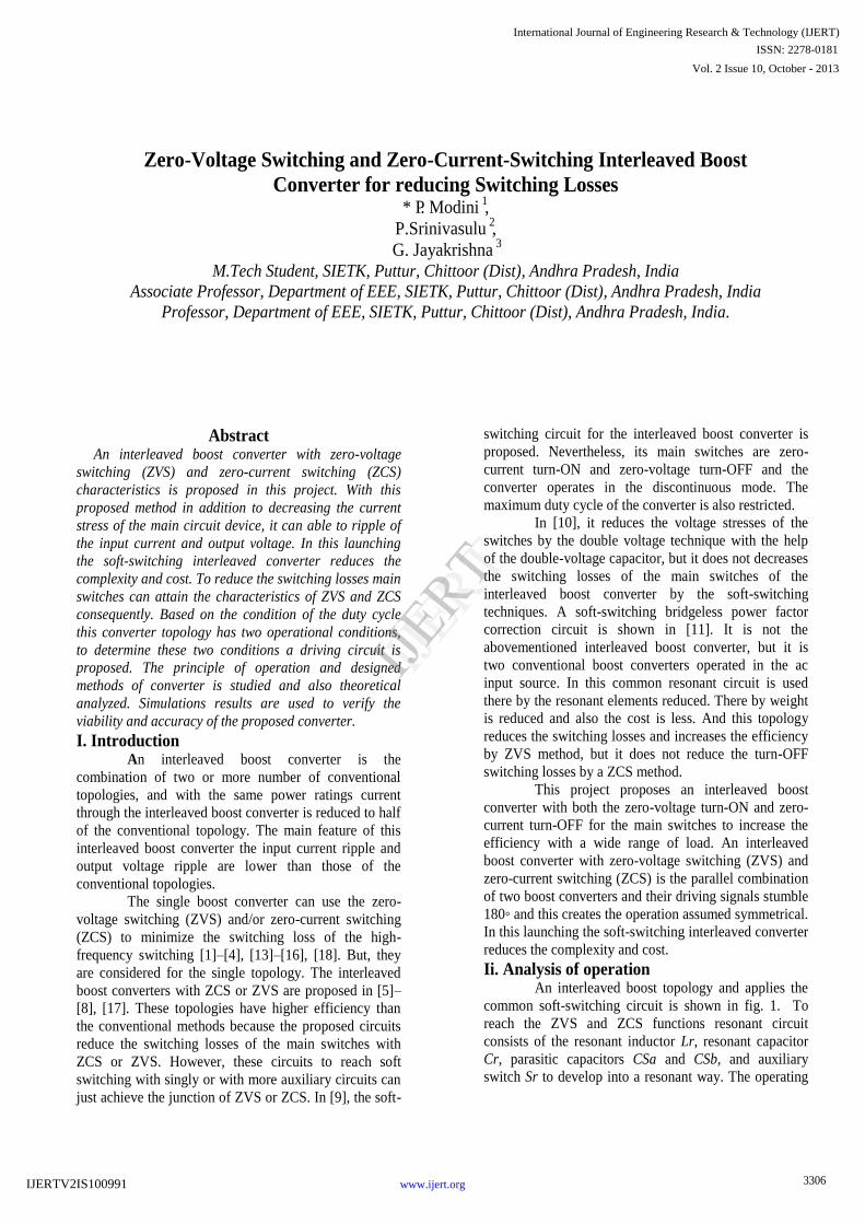
Ii. Analysis of operation An interleaved boost topology and applies the
common soft-switching circuit is shown in fig. 1. To
reach the ZVS and ZCS functions resonant circuit
consists of the resonant inductor Lr, resonant capacitor
Cr, parasitic capacitors CSa and CSb, and auxiliary
switch Sr to develop into a resonant way. The operating
3306
International Journal of Engineering Research & Technology (IJERT)
Vol. 2 Issue 10, October - 2013
IJERT
IJERT
ISSN: 2278-0181
www.ijert.orgIJERTV2IS100991
modes of this circuit, depending on the duty cycle of the
main switch is shown in fig.2.
Fig. 1 A novel interleaved boost converter with
characteristics of zero-voltage switching and zero-
current switching.
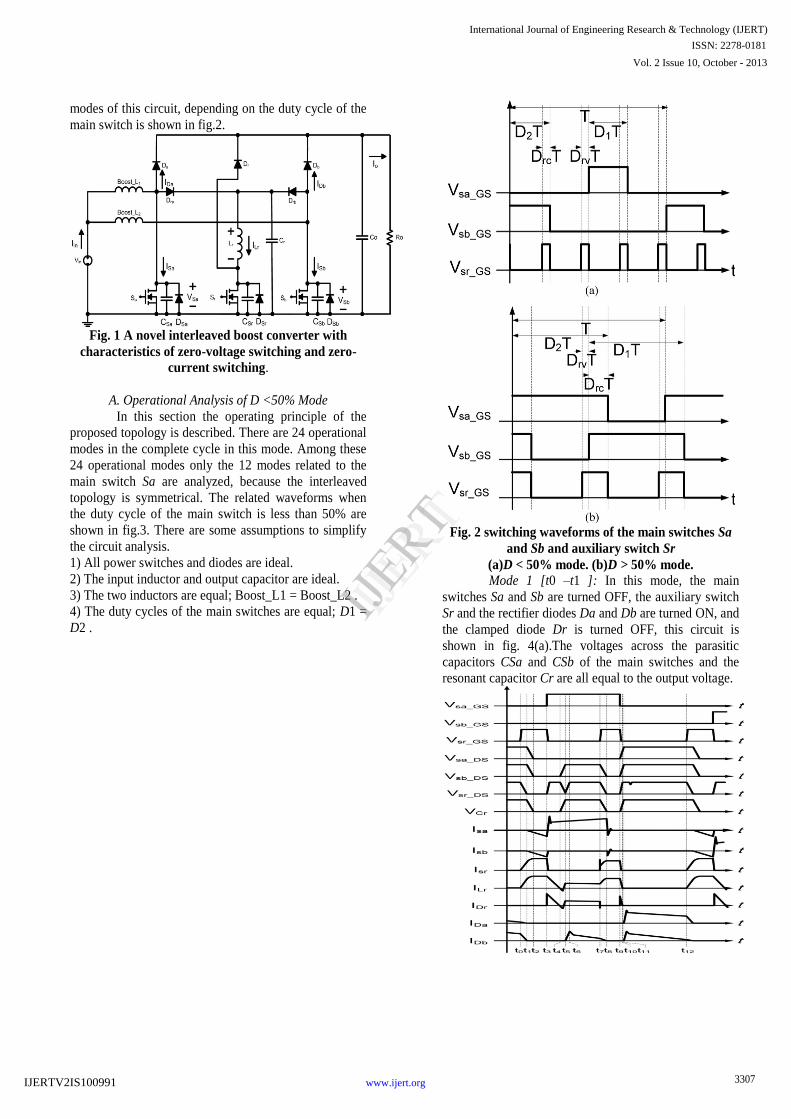
A. Operational Analysis of D <50% Mode
In this section the operating principle of the
proposed topology is described. There are 24 operational
modes in the complete cycle in this mode. Among these
24 operational modes only the 12 modes related to the
main switch Sa are analyzed, because the interleaved
topology is symmetrical. The related waveforms when
the duty cycle of the main switch is less than 50% are
shown in fig.3. There are some assumptions to simplify
the circuit analysis.
1) All power switches and diodes are ideal.
2) The input inductor and output capacitor are ideal.
3) The two inductors are equal; Boost_L1 = Boost_L2 .
4) The duty cycles of the main switches are equal; D1 =
D2 .
Fig. 2 switching waveforms of the main switches Sa
and Sb and auxiliary switch Sr
(a)D < 50% mode. (b)D > 50% mode.
Mode 1 [t0 –t1 ]: In this mode, the main
switches Sa and Sb are turned OFF, the auxiliary switch
Sr and the rectifier diodes Da and Db are turned ON, and
the clamped diode Dr is turned OFF, this circuit is
shown in fig. 4(a).The voltages across the parasitic
capacitors CSa and CSb of the main switches and the
resonant capacitor Cr are all equal to the output voltage.
3307
International Journal of Engineering Research & Technology (IJERT)
Vol. 2 Issue 10, October - 2013
IJERT
IJERT
ISSN: 2278-0181
www.ijert.orgIJERTV2IS100991
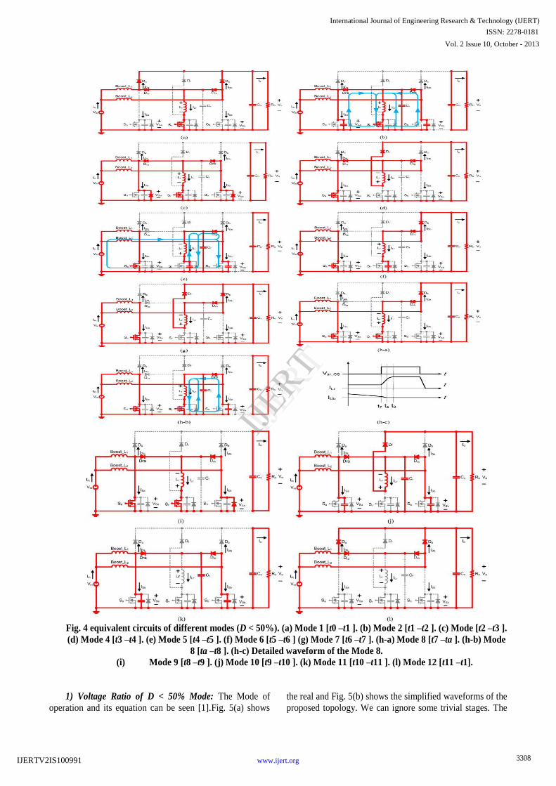
Fig. 4 equivalent circuits of different modes (D < 50%). (a) Mode 1 [t0 –t1 ]. (b) Mode 2 [t1 –t2 ]. (c) Mode [t2 –t3 ].
(d) Mode 4 [t3 –t4 ]. (e) Mode 5 [t4 –t5 ]. (f) Mode 6 [t5 –t6 ] (g) Mode 7 [t6 –t7 ]. (h-a) Mode 8 [t7 –ta ]. (h-b) Mode
8 [ta –t8 ]. (h-c) Detailed waveform of the Mode 8.
(i) Mode 9 [t8 –t9 ]. (j) Mode 10 [t9 –t10 ]. (k) Mode 11 [t10 –t11 ]. (l) Mode 12 [t11 –t1].
1) Voltage Ratio of D < 50% Mode: The Mode of
operation and its equation can be seen [1].Fig. 5(a) shows
the real and Fig. 5(b) shows the simplified waveforms of the
proposed topology. We can ignore some trivial stages. The
3308
International Journal of Engineering Research & Technology (IJERT)
Vol. 2 Issue 10, October - 2013
IJERT
IJERT
ISSN: 2278-0181
www.ijert.orgIJERTV2IS100991
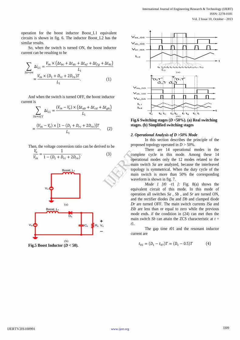
operation for the boost inductor Boost_L1 equivalent
circuits is shown in fig. 6. The inductor Boost_L2 has the
similar results.
So, when the switch is turned ON, the boost inductor
current can be resulting to be
∑ ( )
( )
( )
And when the switch is turned OFF, the boost inductor
current is
∑ ( ) ( )
( ) [ ( )]
( )
Then, the voltage conversion ratio can be derived to be
( ) ( )
Fig.5 Boost Inductor (D < 50).
Fig.6 Switching stages (D <50%). (a) Real switching
stages. (b) Simplified switching stages
2. Operational Analysis of D >50% Mode
In this section describes the principle of the
proposed topology operated in D > 50%.
There are 14 operational modes in the
complete cycle in this mode. Among these 14
operational modes only the 12 modes related to the
main switch Sa are analyzed, because the interleaved
topology is symmetrical. When the duty cycle of the
main switch is more than 50% the corresponding
waveform is shown in fig. 7.
Mode 1 [t0 –t1 ]: Fig. 8(a) shows the
equivalent circuit of this mode. In this mode of
operation all switches Sa , Sb , and Sr are turned ON,
and the rectifier diodes Da and Db and clamped diode
Dr are turned OFF. The main switch currents ISa and
ISb are less than or equal to zero while the previous
mode ends. if the condition in (24) can met then the
main switch Sb can attain the ZCS characteristic at t =
t1.
The gap time t01 and the resonant inductor
current are
( ) ( ) ( )
3309
International Journal of Engineering Research & Technology (IJERT)
Vol. 2 Issue 10, October - 2013
IJERT
IJERT
ISSN: 2278-0181
www.ijert.orgIJERTV2IS100991
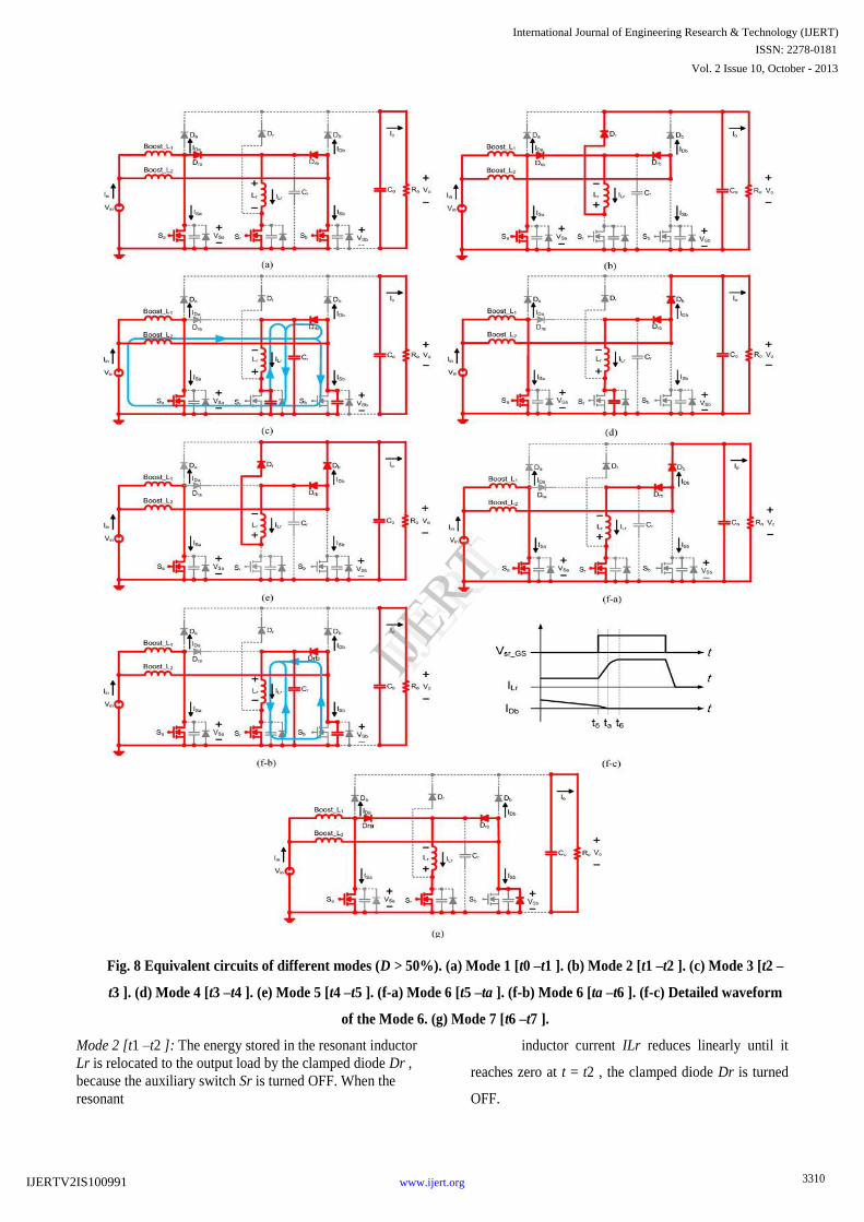
Fig. 8 Equivalent circuits of different modes (D > 50%). (a) Mode 1 [t0 –t1 ]. (b) Mode 2 [t1 –t2 ]. (c) Mode 3 [t2 –
t3 ]. (d) Mode 4 [t3 –t4 ]. (e) Mode 5 [t4 –t5 ]. (f-a) Mode 6 [t5 –ta ]. (f-b) Mode 6 [ta –t6 ]. (f-c) Detailed waveform
of the Mode 6. (g) Mode 7 [t6 –t7 ].
Mode 2 [t1 –t2 ]: The energy stored in the resonant inductor
Lr is relocated to the output load by the clamped diode Dr ,
because the auxiliary switch Sr is turned OFF. When the
resonant
inductor current ILr reduces linearly until it
reaches zero at t = t2 , the clamped diode Dr is turned
OFF.
3310
International Journal of Engineering Research & Technology (IJERT)
Vol. 2 Issue 10, October - 2013
IJERT
IJERT
ISSN: 2278-0181
www.ijert.orgIJERTV2IS100991
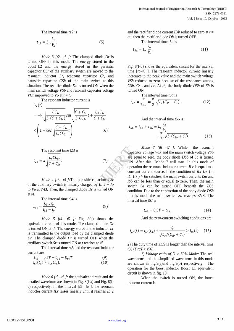
The interval time t12 is
( )
Mode 3 [t2 –t3 ]: The clamped diode Dr is
turned OFF in this mode. The energy stored in the
boost_L2 and the energy stored in the parasitic
capacitor CSr of the auxiliary switch are moved to the
resonant inductor Lr, resonant capacitor Cr, and
parasitic capacitor CSb of the main switch at this
situation. The rectifier diode Db is turned ON when the
main switch voltage VSb and resonant capacitor voltage
VCr improved to Vo at t = t3.
The resonant inductor current is
( )
√
( ) √
( √
) ( )
The resonant time t23 is
√
( )
Mode 4 [t3 –t4 ]:The parasitic capacitor CSr
of the auxiliary switch is linearly charged by IL 2 − Io
to Vo at t>t3. Then, the clamped diode Dr is turned ON
at t4.
The interval time t34 is
( )
Mode 5 [t4 –t5 ]: Fig. 8(e) shows the
equivalent circuit of this mode. The clamped diode Dr
is turned ON at t4. The energy stored in the inductor Lr
is transmitted to the output load by the clamped diode
Dr. The clamped diode Dr is turned OFF when the
auxiliary switch Sr is turned ON at t reaches to t5.
The interval time t45 and the resonant inductor
current are
( ) ( ) ( ) ( )
Mode 6 [t5 –t6 ]: the equivalent circuit and the
detailed waveform are shown in Fig. 8(f-a) and Fig. 8(f-
c) respectively. In the interval [t5– ta ], the resonant
inductor current ILr raises linearly until it reaches IL 2
and the rectifier diode current IDb reduced to zero at t =
ta , then the rectifier diode Db is turned OFF.
The interval time t5a is
( )
Fig. 8(f-b) shows the equivalent circuit for the interval
time [ta–t6 ]. The resonant inductor current linearly
increases to the peak value and the main switch voltage
VSb reduced to zero because of the resonance among
CSb, Cr , and Lr. At t6, the body diode DSb of Sb is
turned ON.
The interval time t6a is
√ ( ) ( )
And the interval time t56 is
√ ( ) ( )
Mode 7 [t6 –t7 ]: While the resonant
capacitor voltage VCr and the main switch voltage VSb
are equal to zero, the body diode DSb of Sb is turned
ON. After this Mode 7 will start. In this mode of
operation the resonant inductor current ILr is equal to a
constant current source. If the condition of iLr (t6 ) ≈
iLr (t7 ) ≥ Iin satisfies, the main switch currents ISa and
ISb can be less than or equal to zero. Then, the main
switch Sa can be turned OFF beneath the ZCS
condition. Due to the conduction of the body diode DSb
in this mode the main switch Sb reaches ZVS. The
interval time t67 is
( )
And the zero-current switching conditions are
( ) ( )
√ ( )⁄ ( ) ( )
2) The duty time of ZCS is longer than the interval time
t56 (DrcT > t56).
1) Voltage ratio of D > 50% Mode: The real
waveforms and the simplified waveforms in this mode
are shown in fig.9(a)and fig,9(b) respectively . The
operation for the boost inductor Boost_L1 equivalent
circuit is shown in fig. 10.
When the switch is turned ON, the boost
inductor current is
3311
International Journal of Engineering Research & Technology (IJERT)
Vol. 2 Issue 10, October - 2013
IJERT
IJERT
ISSN: 2278-0181
www.ijert.orgIJERTV2IS100991
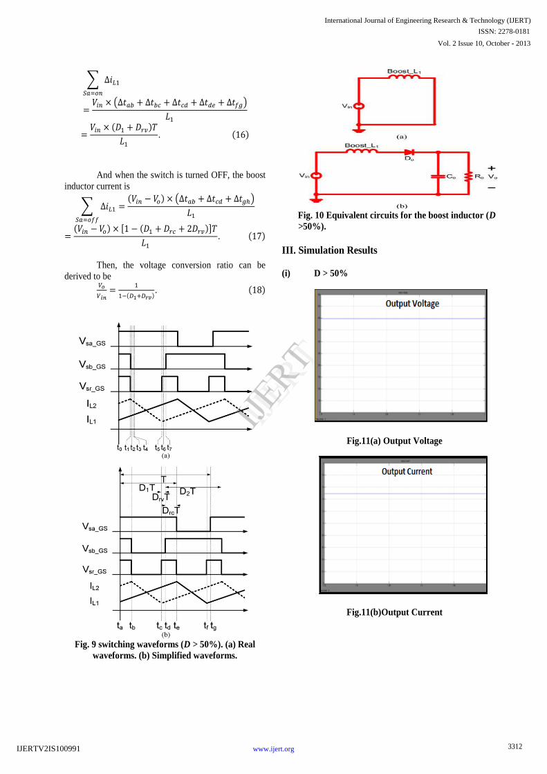
∑
( )
( )
( )
And when the switch is turned OFF, the boost
inductor current is
∑ ( ) ( )
( ) [ ( )]
( )
Then, the voltage conversion ratio can be
derived to be
( ) ( )
Fig. 9 switching waveforms (D > 50%). (a) Real
waveforms. (b) Simplified waveforms.
Fig. 10 Equivalent circuits for the boost inductor (D
>50%).
III. Simulation Results
(i) D > 50%
Fig.11(a) Output Voltage
Fig.11(b)Output Current
3312
International Journal of Engineering Research & Technology (IJERT)
Vol. 2 Issue 10, October - 2013
IJERT
IJERT
ISSN: 2278-0181
www.ijert.orgIJERTV2IS100991

Fig.11(c)Input Voltage
Fig.11(d) Mosfet 1 and Diode 1 Voltage
Fig.11(e)Mosfet 2 and Diode 2 Voltage
Fig.11(f)Mosfet1 voltage and current
Fig.11(g)Mosfet2 voltage and current
II (D<50%) Mode
Fig.11(h)Output Voltage
Fig.11(i)Mosfet1 voltage and diode1 voltage
3313
International Journal of Engineering Research & Technology (IJERT)
Vol. 2 Issue 10, October - 2013
IJERT
IJERT
ISSN: 2278-0181
www.ijert.orgIJERTV2IS100991
Fig.11(j)Mosfet2 voltage and diode2 voltage
Fig.11(k)Output current
Iv. Conclusion
A novel interleaved boost converter with zero-
voltage switching and zero-current-switching functions
is proposed in this project. The duty cycle of this
proposed topology can be more or less than 50%. It has
many characteristics. The main switches Sa and Sb can
achieve both ZVS and ZCS conditions. With this
method achieve the voltage stress of all switches is
equal to the output voltage. The switching functions
ZVS or ZCS function can be achieved just by the
adjustment of the driving circuit. The efficiency of this
topology is improved to 95.5% with output power of
400W and input voltage of 250V.
V. References
[1] G. C. Hua, W. A. Tabisz, C. S. Leu, N. Dai, R. Watson,
and F. C. Lee, “Development of a DC distributed power
system,” in Proc. IEEE 9th Annu. Appl. Power Electron. Conf.
Expo., Feb. 1994, vol. 2, pp. 763–769.
[2] C. M. Wang, “A new single-phase ZCS-PWM boost
rectifier with high power factor and low conduction losses,”
IEEE Trans. Ind. Electron., vol. 53, no. 2, pp. 500–510, Apr.
2006.
[3] H. M. Suryawanshi, M. R. Ramteke, K. L. Thakre, and V.
B. Borghate, “Unity-power-factor operation of three-phase
AC–DC soft switched converter based on boost active clamp
topology in modular approach,” IEEE Trans. Power
Electron., vol. 23, no. 1, pp. 229–236, Jan. 2008.
[4] C. J. Tseng andC. L.Chen, “A passive lossless snubber
cell for nonisolated PWM DC/DC converters,” IEEE Trans.
Ind. Electron., vol. 45, no. 4, pp. 593–601, Aug. 1998.
[5] Y.-C. Hsieh, T.-C. Hsueh, and H.-C. Yen, “An interleaved
boost converter with zero-voltage transition,” IEEE Trans.
Power Electron., vol. 24, no. 4, pp. 973–978, Apr. 2009.
[6] C. M. de Oliveira Stein, J. R. Pinheiro, and H. L. Hey, “A
ZCT auxiliary commutation circuit for interleaved boost
converters operating in critical conduction mode,” IEEE
Trans. Power Electron., vol. 17, no. 6, pp. 954– 962, Nov.
2002.
[7] C. A. Canesin and F. A. S. Goncalves, “A 2kW
Interleaved ZCS-FM boost rectifier digitally controlled by
FPGA device,” in Proc. IEEE Power Electron. Spec. Conf.,
Jul. 2006, vol. 2, pp. 1382–1387.
[8] W. Li and X. He, “ZVT interleaved boost converters for
high-efficiency, high step-up DC DC conversion,” IET
Electron. Power Appl., vol. 1, no. 2, pp. 284–290, Mar. 2007.
[9] G. Yao, A. Chen, and X. He, “Soft switching circuit for
interleaved boost converters,” IEEE Trans. Power Electron.,
vol. 22, no. 1, pp. 80–86, Jan. 2007.
[10] J. Yungtaek and M. M. Jovanovic, “Interleaved PFC
boost converter with intrinsic voltage-doubler characteristic,”
in Proc. IEEE Power Electron. Spec. Conf., Jun. 2006, pp.
1888–1894.
[11] H.-Y. Tsai, T.-H. Hsia, and D. Chen, “A novel soft-
switching bridgeless power factor correction circuit,” in Proc.
Eur. Conf. Power Electron. Appl., Sep. 2007, pp. 1–10.
[12] S. S. Saha, B. Majumdar, T. Halder, and S. K. Biswas,
“New fully softswitched
boost-converter with reduced conduction losses,” in Proc.
IEEE Int. Conf. Power Electron. Drives Syst., 2005, vol. 1,
pp. 107–112.
[13] G. Hua, C.-S. Leu, Y. Jiang, and F. C. Y. Lee, “Novel
zero-voltagetransition PWM converters,” IEEE Trans. Power
Electron., vol. 9, no. 2, pp. 213–219, Mar. 1994.
[14] E. Adib and H. Farzanehfard, “Family of soft-switching
PWM converters with current sharing in switches,” IEEE
Trans. Power Electron., vol. 24, no. 4, pp. 979–985, Apr.
2009.
[15] E. Adib and H. Farzanehfard, “Zero-voltage-transition
PWM converters with synchronous rectifier,” IEEE Trans.
Power Electron., vol. 25, no. 1, pp. 105–110, Jan. 2010.
[16] S.-H. Park, S.-R. Park, J.-S. Yu, Y.-C. Jung, and C.-Y.
Won, “Analysis and design of a soft-switching boost
converter with an HI-bridge auxiliary resonant circuit,” IEEE
Trans. Power Electron., vol. 25, no. 8, pp. 2142– 2149, Aug.
2010.
[17] S. Park and S. Choi, “Soft-switched CCM boost
converters with high voltage gain for high-power
applications,” IEEE Trans. Power Electron., vol. 25, no. 5,
pp. 1211–1217, May 2010.
[18] I. Aksoy, H. Bodur, and A. FarukBakan, “AnewZVT-
ZCT-PWMDC–DC converter,” IEEE Trans. Power Electron.,
vol. 25, no. 8, pp. 2093–2105, Aug. 2010.
[19] M. Kazimierczuk and D. Czarkowski, Resonant Power
Converter. Hoboken, NJ: Wiley, 2011.
[20] I. Batarseh, Power Electronic Circuits. Hoboken, NJ:
Wiley, 2004.
3314
International Journal of Engineering Research & Technology (IJERT)
Vol. 2 Issue 10, October - 2013
IJERT
IJERT
ISSN: 2278-0181
www.ijert.orgIJERTV2IS100991

[21] N. Mohan, T. M. Undeland, and W. P. Robbins, Power
Electronic- Converters, Applications, and Design. Hoboken,
NJ: Wiley, 2007.
[22] D. W. Hart, Introduction to Power Electronics.
Englewood Cliffs, NJ: Prentice-Hall, 1997.
P.Modini received B.Tech degree in
Electrical and Electronics Engineering
from Jawaharlal Nehru Technological
University, Anantapur, India in 2009.
Currently she is pursuing M.Tech (Power
Electronics) in Siddharth Institute of Engineering and
Technology, Puttur, India.
P.Srinivasulu received B.Tech, degree in
Electrical and Electronics Engineering
from JNTUH University, and M.Tech
degrees in Power Electronics and
Industrial Drives from Satyabhama
University, Chennai, Currently he is with department
of Electrical and Electronics Engineering, Siddharth
Institute of Engineering and Technology, Puttur,
India. His research interests include Power systems
and power electronics.
G.Jayakrishna received B.Tech, M.Tech and
Ph.D degrees in Electrical Engineering from
Jawaharlal Nehru Technological University,
Anantapur, India in 1993, 2004 and 2013
respectively. Currently he is with department
of Electrical and Electronics Engineering,
Siddharth Institute of Engineering and Technology,
Puttur, India. His research interests include
Power Quality, Electrical drives and Power
Systems.
3315
International Journal of Engineering Research & Technology (IJERT)
Vol. 2 Issue 10, October - 2013
IJERT
IJERT
ISSN: 2278-0181
www.ijert.orgIJERTV2IS100991