Y. Furukawa Y. Mori T. Kataoka (Eds.) Precision … · PRECISION SCIENCE AND TECHNOLOGY FOR PERFECT...
15
Y. Furukawa Y. Mori T. Kataoka (Eds.) Precision Science and Technology for Perfect Surfaces Proceedings of the 9th International Conference on Production Engineering (9th ICPE) Senri Life Science Center, Osaka, Japan August 29 - September 1,1999 UNIVERSITATSBIBLIOTHEK HANNOVER TECHNISCHE INFORMATIONSBIBLIOTHEK Sponsored by The Japan Society for Precision Engineering (JSPE) Supported by The Commemorative Association for the Japan World Exposition (1970) Published by The Japan Society for Precision Engineering (JSPE) JSPE Publication Series No.3
-
Upload
phungtuyen -
Category
Documents
-
view
216 -
download
0
Transcript of Y. Furukawa Y. Mori T. Kataoka (Eds.) Precision … · PRECISION SCIENCE AND TECHNOLOGY FOR PERFECT...
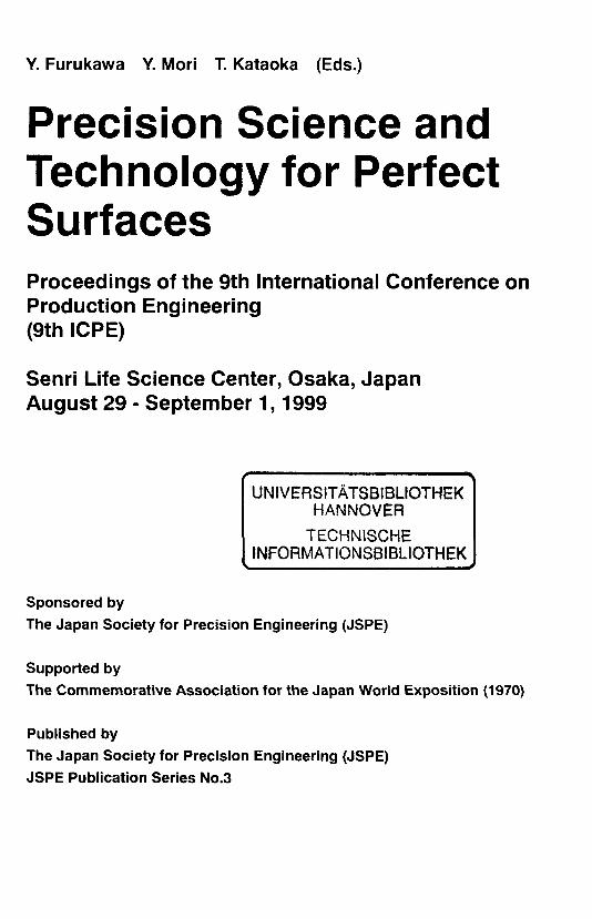
Y. Furukawa Y. Mori T. Kataoka (Eds.)
Precision Science andTechnology for PerfectSurfacesProceedings of the 9th International Conference onProduction Engineering(9th ICPE)
Senri Life Science Center, Osaka, JapanAugust 29 - September 1,1999
UNIVERSITATSBIBLIOTHEKHANNOVER
TECHNISCHEINFORMATIONSBIBLIOTHEK
Sponsored by
The Japan Society for Precision Engineering (JSPE)
Supported by
The Commemorative Association for the Japan World Exposition (1970)
Published by
The Japan Society for Precision Engineering (JSPE)
JSPE Publication Series No.3
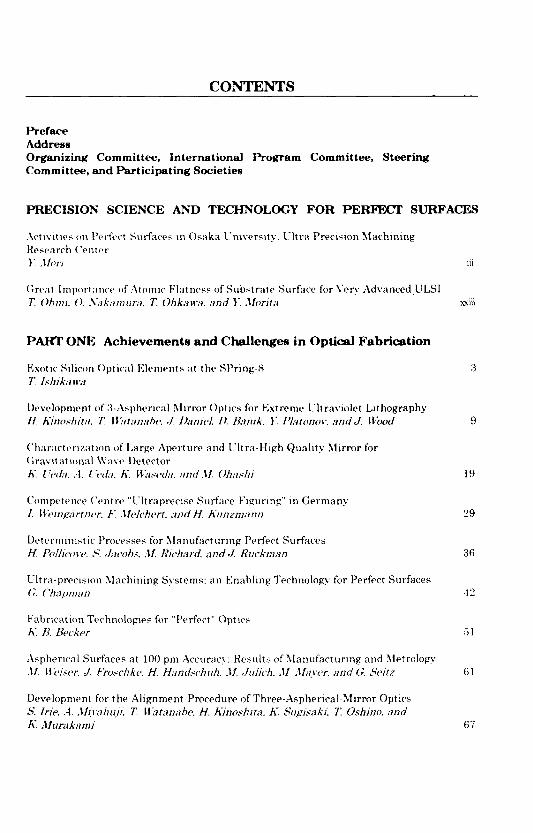
CONTENTS
PrefaceAddressOrganizing Committee, International Program Committee, SteeringCommittee, and Participating Societies
PRECISION SCIENCE AND TECHNOLOGY FOR PERFECT SURFACES
Activities on Perfect Surfaces in Osaka University. Ultra Precision MachiningResearch Center}'. Mori iii
Great Importance of Atomic Flatness of Substrate Surface for Very Advanced ULSIT. Ohmi. (). Xakamura. T. Ohkawa. and Y. Morita xxiii
PART ONE Achievements and Challenges in Optical Fabrication
Exotic Silicon Optical Elements at the SPrmg-8 3T. Ishikawa
Development of 3-Aspherical Mirror Optics for Extreme Ultraviolet Lithography//. Kinoshila. T Watanabc. J Daniel. 1). Bajuk. Y. Phuonov. and J. Wood 9
Characterization of Large Aperture and Ultra-High Quality Mirror forCiravitational Wave DetectorA'. Urda. A. i'eda. K. Uaseda. andM. Ohashi 19
Competence Centre "Ultraprecise Surface Figuring" in Germany/. Wi'inparttwr. F. Me/chert, and H. Kunzmann 29
Deterministic Processes for Manufacturing Perfect SurfacesH. Pollicovt'. S. Jacobs. M. Richard, and J. Ruckman 36
Ultra-precision Machining Systems: an Enabling Technology for Perfect SurfacesO. Chapman 42
Fabrication Technologies for "Perfect" OpticsA". II Becker 51
Aspherical Surfaces at 100 pm Accuracy: Results of Manufacturing and MetrologyM. Weiser. J. Froschke. H. Handschuh. M. Julich. M. Mayer, and G. Seitz 61
Development for the Alignment Procedure of Three-Aspherical-Mirror Optics5. Irie. A. Miyahuji. T. Watanahe. H. Kinoshita. K. Supisaki. T. Oshino. andK. Murakami 67
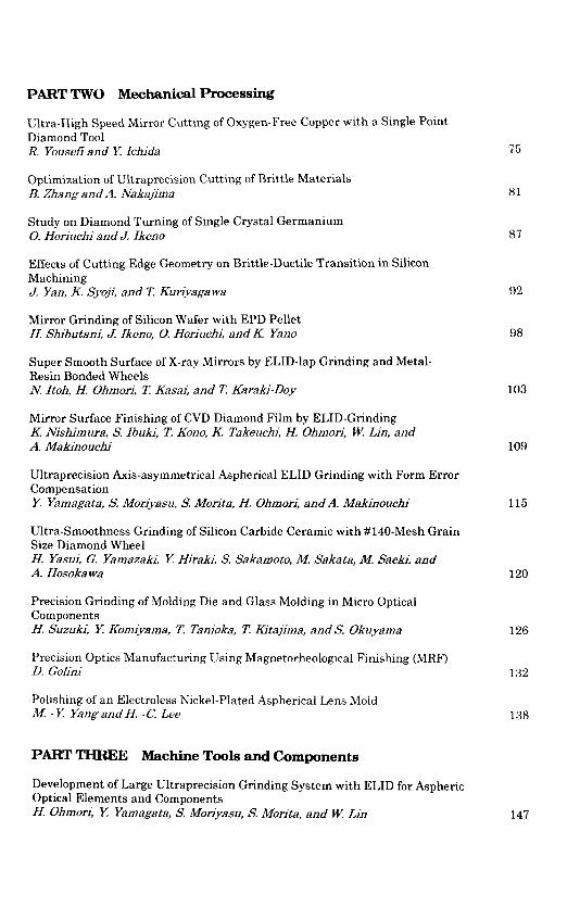
PART TWO Mechanical Processing
Ultra-High Speed Mirror Cutting of Oxygen-Free Copper with a Single PointDiamond ToolR. Yousefi and Y. Ichida 75
Optimization of Ultraprecision Cutting of Brittle MaterialsB. Zhang and A. Nakajima 81
Study on Diamond Turning of Single Crystal GermaniumO. Horiuchi and J. Ikeno 87
Effects of Cutting Edge Geometry on Brittle-Ductile Transition in SiliconMachiningJ. Yan, K. Syoji, and T. Kuriyagawa 92
Mirror Grinding of Silicon Wafer with EPD PelletH. Shibutani, J. Ikeno, O. Horiuchi, and K. Yano 98
Super Smooth Surface of X-ray Mirrors by ELID-lap Grinding and Metal-Resin Bonded WheelsN. Itoh, H. Ohmori, T. Kasai, and T. Karaki-Doy 103
Mirror Surface Finishing of CVD Diamond Film by ELID-GrindingK. Nishimura, S. Ibuki, T. Kono, K. Takeuchi, H. Ohmori, W. Lin, andA. Makinouchi 109
Ultraprecision Axis-asymmetrical Aspherical ELID Grinding with Form ErrorCompensationY. Yamagata, S. Moriyasu, S. Morita, H. Ohmori, and A. Makinouchi 115
Ultra-Smoothness Grinding of Silicon Carbide Ceramic with #140-Mesh GrainSize Diamond WheelH. Yasui, G. Yamazaki, Y. Hiraki, S. Sakamoto, M. Sakata, M. Saeki, andA. Hosokawa 120
Precision Grinding of Molding Die and Glass Molding in Micro OpticalComponentsH. Suzuki, Y. Komiyama, T. Tanioka, T. Kitajima, and S. Okuyama 126
Precision Optics Manufacturing Using Magnetorheological Finishing (MRF)D. Golini 132
Polishing of an Electroless Nickel-Plated Aspherical Lens MoldM. -Y. Yang and H. -C. Lee 138
PART THREE Machine Tools and Components
Development of Large Ultraprecision Grinding System with ELID for AsphericOptical Elements and ComponentsH. Ohmori, Y. Yamagata, S. Moriyasu, S. Morita, and W. Lin 147
Development and Characteristics of Fixed Abrasive Polishing Utilizing SmallGrinding Tools with ELID for Final Finish Process of Aspheric Optical ElementsC. Liu, H. Ohmori, W. Lin, N. Itoh, T. Kasai, and K. Horio 153
Manufacture of Fresnel Lens by Ultraprecision Machining Center Based onFriction-free Servo MechanismN. Sornsuwit, Y. Takeuchi, T. Kawai, K. Sawada, and T. Sata 159
An Ultraprecision Machine Tool with Active Control Aerostatic Guideways forImproving Quality of Machined SurfaceH. Mizumoto, S. Inoue, S. Arii, Y. Kami, and M. Yabuya 165
Ultraprecision Lap-Grinding with PhotodressingS. Moriyasu, S. Morita, Y. Yamagata, H. Ohmori, A. Makinouchi, and N. Itoh 171
Development of Discontinuous Grinding Wheel with Multi-Porous GroovesJ. Kim 175
Forming of Texture Surface Composed of Micro Dents Using Indenting ToolA. Inada, M. Masuda, and T. Miyamoto 181
Giant Magnetostrictive Positioner for Single Diamond Turning of SiliconSubstrateH. Eda, J. Shimizu, L. Zhou, Y. Takimoto, and A. Muroya 187
A Study on Run-out Error in Externally Pressurized Journal Gas BearingH. Tomita, K. Koizumi, and K. Konosu 193
Non-contact Handling System for Thin Plate Utilizing Electrostatic ForceF. Poh and T. Higuchi 199
PART FOUR Physical/ Chemical Processing
Development of Numerically Controlled EEM (Elastic Emission Machining)System for Ultraprecision Figuring and Smoothing of Aspherical SurfacesY. Mori, K. Yamauchi, K Sugiyama, K. Inagaki, S. Shimada, J. Uchikoshi,H. Mimura, T. Imai, and K Kanemura 207
Development of Numerically Controlled Plasma CVM (Chemical VaporizationMachining) System for Fabrication of Ultra Precision Optical DevicesY. Mori, K. Yamamura, and Y. Sano 213
Plasma Chemical Vaporization Machining with a Pipe Electrode for LargeOpticsH. Takino, N. Shibata, T. Kobayashi, H. Itoh, H. Tanaka, A. Koike, K. Nakano,K. Yamamura, Y. Sano, and Y. Mori 219
Slicing of Functional Materials by Plasma CVM (Chemical VaporizationMachining)Y. Mori, K. Yamamura, and Y. Sano 225
Plasma Jet Chemical Etching - a Tool for the Figuring of Optical PrecisionAspheresG. Boehm, W. Frank, A. Schindler, A. Nickel. H.J. Thomas. F. Bigl. andM. Weiser 231
Development of Ultra-Precision and Ultra-Clean Electro-Chemical ProcessingMethod Using Hydroxyl Ion in Ultrapure WaterY. Mori, H. Goto, K. Hirose. I. Kobata. and Y. Toma 237
Nanometer Precision (Reactive) Ion Beam Figuring of (Aspherical) OpticalSurfacesA. Schindler, T. Haensel. D. Flamm, A. Nickel. H. J. Thomas, andF. Bigl 243
Sub-Nanometer Polishing of Optical Surfaces by Ion Beam PlanarizationTechniqueR. Fechner, A. Schindler, T. Haensel, and F. Bigl 249
Ion Beam Processing of Nickel-Phosphor Alloy Film Deposited on the Al Plate byElectroless Plating MethodJ. Taniguchi, R, Kimura, C. Kageyama, and I. Miyamoto 255
Radiation-Resistant Optical Surface Fabricated by Ion Beam EtchingT. Kamimura, K. Nakai, M. Yoshimura, Y. Mori, T. Sasaki, H. Yoshida.M. Nakatsuka, M. Tanaka, S. Toda, M. Tanaka, and K Yoshida 261
UV Laser Ablative Figuring of Precise OpticsK.Tokumura, T. Jitsuno, M. Nakatsuka, G. Yoon, andH. Tamamura 267
Large Scale Single-Crystal and Extremely Smooth SiC Surface Produced byHe tero-Epitaxial Growth and its Applicability to Optical ElementsA Moronuki, A. Kakuta, and Y. Furukawa 273
A Study on the SiC Hetero-Epitaxial Growth Process on Silicon SubstrateA. Kakuta, H. Miyakoshi, N. Moronuki, and Y. Furukawa 279
Multilayer X-ray Optics for High Energy Third Generation Synchrotron Sources:the State of the ArtE. Ziegler, Ch. Mora we, O. Hignette, P. Cloetens, and R. Tucoulou 285
Deposition Shutter Control for Figured Multilayer FabricationT. Hatano, H. Umetsu. and'M. Yamamoto 292
PART FIVE Figure and Surface Testing
Nanometer Precision in Large Surface ProfilometryP. Z. Takacs 301
Ultra-Precise Scanning Technique for Surface Testing in the Nanometric Range/. Weingartner andM. Schulz 311
Study of Optimum Mounting Positions of Sensor Probes of Three-Point MethodX. Cui, O. Horiuchi, andJ. Ikeno 317
Laser Beam Straight Datum with Nanometric Accuracy -Analytical Estimationof Ultimate Brightness-es Uchikoshi, S. Shimada, K. Arimoto, and A. Komura 323
Sub-nanometer Interferometry for Aspheric Mirror FabricationG. E. Sommargren, D. W. Phillion, and E. W. Campbell 329
Development of Phase-Shifting Point Diffraction Interferometry Method withFiber Point SourcesY. Oshikane, K. Ikeda, T. Kataoka, K. Endo, and H. Inoue 336
Precise Surface Measurement by Local Sampling Phase Shifting InterferometryY. Otani, H. Mori, and T. Yoshizawa 342
Flatness Measurement by Moire Technique for Large Diameter WaferH. Fujiwara, Y. Kodera, Y. Otani, and T. Yoshizawa 348
A High-Precision Coordinate Measurement Machine for Aspherical OpticsM. Negishi, K. Watanabe, K. Matsusita, T. Kasahara, and K. Hosaka 354
Development of an Ultra-Precission 3D-CMM with the Repeatability ofNanometer OrderH. Shiozawa, and Y. Fukutomi 360
Development of Ultraprecision Contact-type Form Measuring Probe forOnmachine MeasurementS. Moriyasu, S. Morita, Y. Yamagata, H. Ohmori, J. Kato, I. Yamaguchi, andA. Makinouchi 366
Evaluation of Si Wafer Surface Using a New Apparatus for Measuring Particleof the Order of NanometerH. An, S. Sasaki, Y. Mori, T. Kataoka, K Endo, H. Inoue, andK Yamauchi 372
Measurement of Ultra Fine Particles on the Si Wafer Surface Using Laser LightScatteringH. Inoue, T. Kataoka, K. Endo, Y. Oshikane, T. Takemura, Y. Mori, H. An, andS. Sasaki 378
Analysis of Laser Scattered Defect Pattern for Optical Measurement of SiliconWafer Surface DefectsS. Takahashi. T. Miyoshi, and Y. Takaya 384
PART SIX Silicon Surface Processing
Qualities of 400mm-Diameter As-Sliced Wafers and Quality Changes ThroughWafer Shaping ProcessH. Oishi, K. Asakawa, andJ. Matsuzaki 393
Current CMP Process and Future NeedsS. Tanaka, M. Kishimoto, and Y. Itoh 399
High Rate Polishing of Silicon Surface using Plasma CVM with Rotary DrumElectrodeH. Takeuchi, T. Okuda, K. Nishikawa, Y. Hojyo, M. Kadono, T. Nukii,K. Yamamura, Y. Sano, and Y. Mori 405
Smooth Si(001) Surfaces Prepared by Glancing Angle Sputtering under Rotationof TargetK. Nakajima, N. Hairuddin, and K. Kimura 411
Flattening Si(001) Surface by Annealing in Molecular H2 AmbientT. Komeda and Y. Kumagai 415
Oxidation Control of Si(100) Surface in Heating-up ProcessK. Nishimura, S. Urabe, and M. Morita 421
Formation Process of Highly Reliable Gate Oxide Using Water Vapor GeneratorSystemO. Nakamura, T. Ohkawa, M. Nakagawa, and T. Ohmi 426
Water Vapor Generator Using Catalytic ReactorK. Kawada, Y. Minami, A. Morimoto, N. Ikeda, O. Nakamura, Y. Shirai, andT. Ohmi 432
Cr2O3 Passivated Gas Tubing System and Installation MethodM. Kitano, O. Nakamura, M. Nagase, Y. Shirai, and T. Ohmi 438
Precise Control of Gas Concentration Ratio in Process ChamberM. Nagase, O. Nakamura, M. Kitano, Y. Shirai, and T. Ohmi 444
Development of Anisotropic Dry Etching Method Using Laser-CollimatedFluorine Radical BeamM. Shimizu, H. Ohmi, K. Yasutake, K. Yamane, R. Tanaka, A. Takeuchi,H. Kakiuchi, K. Yoshii, and Y. Mori 450
PART SEVEN Surface Cleaning and Wet Processing
Advanced Cleaning Strategies for Ultra-clean Silicon SurfacesM. Heyns, T. Bearda, I. Cornelissen, S. De Gendt, L. Loewenstein, P. Mertens,S. Mertens, M. Meuris, M. Schaekers, I. Teerlinck, R. Vos, and K. Wolke 459
Dissolution of Metal into Gas Controlled Ultra Pure WaterM. Toda, K. Shishido, K. Akuto, and T. Ohmi 469
Particle Removal Effect of Hydrogenated Ultrapure Water with MegasonicIrradiationJ. Ida, H. Morita, and T. Ohmi 475
Infrared Monitoring of Hydrocarbons on 300-mm Si WafersM. Endo, H. Yoshida, Y. Maeda, N. Miyamoto, and M. Niwano 480
Scanning Tunneling Microscopy Observations of Hydrogen Terminated Si(001)Surfaces after Wet CleaningK. Endo, K Arima, T. Kataoka, Y. Oshikane, H. Inoue, K. Koba, H. Nakahama,and Y. Mori 485
Flattening of Si(lll) Surface in Oxygen-free Water and Alkaline SolutionsH. Fukidome andM. Matsumura 491
Oxidation and Hydrogen Termination of Si Surface in NH4F SolutionY. Kondo, Y. Kimura, andM. Niwano 495
Precise Wet Etching for Large-Sized WaferM. Miyashita, T. Ohmi, T. Yabune, and H. Kikuyama 501
The Control of Etching Rate for Various SiO2 FilmsT. Kezuka, M. Itano, and T. Ohmi 507
Room Temperature Photoresist Physical Stripping TechnologyS. Ojima, T. Jizaimaru, S. Omae, and T. Ohmi 513
PART EIGHT Thin Film Technology
Optimization of Interfaces in Thin Film Transistors and Thin Film Solar Cellsusing Hot Wire Chemical Vapor DepositionR. E. I. Schropp, B. Stannowski, and J. K. Rath 521
Improved Controllable Range of the Optical and Electrical Properties ofAmorphous Silicon for Solar CellsY. Hishikawa, H. Tarui, andS. Kiyama 531
High-Rate Deposition of Amorphous Si Thin Films by Atmospheric PressurePlasma CVDY. Mori, K. Yoshii, K. Yasutake, H. Kakiuchi, Y. Domoto, H. Tarui, andS. Kiyama 537
High-speed Patterning of Integrated-Type a-Si Solar Cell Sub modules byPlasma CVMS. Nakano, Y. Domoto, H. Tarui, S. Kiyama, Y. Sano. K. Yamamura, and Y. Mori 543
Plasma Treatment Effect on the Off Current Characteristics of an a-Si TFTS. Yabuta, S. Yamakawa, A. Ban, Y. Kataoka, M. Okamoto, H. Kato,M. Katayama, and Y. Ishii 549
Smart Cut®: A Highly Productive SOI Manufacturing TechnologyK. Mitani and N. Tate 555
Gate Oxide Integrity and Buried Oxide Integrity of ADVANTOX™190M. Takamatsu, M. Kainuma, M. Sudou, T. Nakai, H. Emori, and Y. Shimanuki 561
Characterization of Electrically Active Defects at SOI-BOX Interface on High-Dose SIMOX WafersT. Ushiki, K. Kotani, T. Funaki, K. Kawai, and T. Ohmi 567
The Application of the Protective Oxidation and Hydrogen Termination forRelatively Low Temperature Epitaxial GrowthM. Mayusumi, M. Imai, S. Nakahara, and K. Inoue 573
Low-Temperature Growth of Ultra-Thin Silicon Nitride Films for ExtendingScaling Limit of Silicon OxideK. Sekine, Y. Saito, M. Hirayama, and T. Ohmi 579
Advanced Shower Plate Applicable To Radial Line Slot Antenna MicrowaveExcited Plasma ChamberA. Morii, M. Hirayama, and T. Ohmi 584
Control of Transformation Timing of Titanium for VLSI ProcessN. Mizuno, M. Shimizu, C- Lavoie, and C. CabralJr. 590
Deposition of ZnO Film by Using an Atmospheric Pressure Cold PlasmaGeneratorH. G. Teong, Y. Suzaki, T. Shikama, O. Tanaka, T. Kajitani, and H. Koinuma 596
Effect of In-situ He Ion Beam Irradiation on the ITO Films Prepared by IBSMethodY. Suzaki, T. Shikama, O. Tanaka, T. Kajitani, H. Higuchi, and S. Nakamura 601
Ion Beam Sputter Deposition for Growth of Stoichiometric Thin Films of TiNiShape Memory AlloyS. T. DaviesandK. Tsuchiya 606
A Study of the Submicron-Scale Roughening and Smoothing of SemiconductorSurfaces during Ion SputteringF. Frost, A. Schindler, D. Hirsch, and F. Bigl 612
Effects of Argon and Nitrogen Partial Pressure on Internal Stress, Resistivityand Structure of Reactive Sputtered TiN FilmsS. Inoue, H. Takata, andK. Koterazawa 618
Doping of Single Crystalline A1N Thin Films Grown on Si(lll) by Plasma-Assisted MBEA, Takeuchi, M. Ono, K. Yasutake. H. Kakiuchi, and K. Yoshii 624
Creation of Mono-Velocity Neutral Atomic BeamH. Ohmi, K. Yasutake, M. Shimizu, T. Yasukawa, A. Takeuchi. H. Kakiuchi,K. Yoshii, M. Umeno, and Y. Mori 630
PART NINE Atomically Controlled Surface Processing
Nono-Structure Fabrication by Growth Mode ControlY. Aoyagi, H. Isshiki, M. Ishii, and S. Tanaka 639
Strain Engineering of Nanoscale Structures in the Ge/Si SystemF. Liu andM. G. Lagally 648
Mechanical and Current-Assisted Manipulation of Atoms and Molecules using aLow Temperature Scanning Tunneling MicroscopeK. H. Rieder, G. Meyer, L. Bartels, J. Repp, and S. W. Hla 658
Structure Fabrication and Property Measurement on the Nanoscale by STM-Based New MethodsM. Aono 665
AFM Nano-Lithography Using a Current-Controlled Exposure System and aMultilayer Resist SystemM. Ishibashi, S. Heike, N. Sugita, H. Kajiyama, and T. Hashizume 671
Nanometer-Scale Machining of Single-Crystal Silicon Using an Atomic ForceMicroscopeY. Ichida, R. Sato, and K Takahashi Gil
Machining of Small Diametric Deep Hole on Si PlateY. Kita, K. Yoshida, and Y. Miwa 683
Collision Induced-Deposition of N2 on Ni(100) Surface Studied with FTIRT. Takaoka, M. Terahara, and I. Kusunoki 689
Chemically-Assisted Desorption of Hydrogen Atoms on Hydrogen-Terminated SiSurfaceY. Morita, R. Hasunuma. andH. Tokumoto 693
Control of Atomic Defects of TiC by Its Chemical ActivityH. Kuramochi, K. Takami, S. Otani, A. Saito, Y. Kuwahara, M. Aono, andY. Mori 699
Ordering and Reaction of Diacetylene Molecules on a Graphite Surface Observedwith STMY. Okawa andM. Aono 705
A Scanning Tunneling Microscope Tip Made of an Ionic Conductor as a MetalAtom Source to Fabricate NanostructuresK. Terabe. T. Nakayama, N. Iyi. andM. Aono 711
Formation of Nanostructures on Si(110) Surfaces with the Interaction of Cr,0MoleculesM. Yoshim ura and K. Ueda 717
Highly Smooth Surface of Perovskite-Type Oxide Thin Flims Grown byAdvanced Laser Ablation MethodM. Sugiura, K. Uragou, M. Tachiki. Y. Furukawa, M. Nomura, and T. Kobayashi 722
Low Temperature Scanning Tunneling Microscopy Study on the Growth andAtomic Manipulation of NaCl on Vicinal Copper SurfacesG. Meyer, J. Repp, S. Zophel, and K. H. Rieder 728
Nuclei-Step-Flow Growth of Diamond Films by Plasma-Assisted Chemical VaporDeposition MethodT. Hosomi, T. Maki, and T. Kobayashi 733
Characterization and Fabrication of Hydrogen-Terminated Diamond SurfaceProduced by Microwave Plasma CVD MethodT. Takami, I. Kusunoki, M. Nishitani-Gamo, and T. Ando 739
Effect of Low Energy Ions on Structure and Mechanical Properties of DLC FilmsFabricated at Room Temperature by ECR-CVDY. Domoto, H. Yagi, H. Tarui, and S. Kiyama 745
PART TEN Surface Characterization by Beam Techniques
Multi-method Surface Analysis in the lOnm RangeE. Bauer, T. Schmidt, and T. Duden 753
Ultra Trace Element Analysis in Microelectronics with SR-TXRFF. Comin and P. Mangiagalli 763
Atomic-Scale Surface Morphology of Ultrathin Thermal Oxide Formed onSi(100) SurfaceH. Nohira, M. Fujimura, K. Inoue, and T. Hattori 769
Initial Stage of Oxidation of Si(001)-2xl Surface and Amorphous Si SurfaceStudied by X-Ray Photoelectron SpectroscopyY. Harada, M. Niwa, T. Nagatomi, and R. Shimizu 115
Determination of the Energy Distribution of Interface States in the Si ForbiddenGap by XPS Measurements under BiasA. Asano, T. Kubota, Y. Nishioka, and H. Kobayashi 781
Newly Applied X-ray Standing Wave Analysis to the YSZ CrystalA.Saito, Y. Kuwahara, M. Aono, and T. Matsushita 787
Development of Evaluation Method for Ultra Precision Machined Surfaces byPhoto-Reflectance SpectraK. Inagaki, K. Tahara, Y. Fujimoto, K. Endo, K. Sugiyama, K. Hirose, and Y. Mori 792
Structural Study of Ni/YSZ(001) by Coaxial Impact-Collision Ion ScatteringSpectroscopyA. Saito, K. Yamasaki, Y. Kuwahara, andM. Aono 796
Hydrogen Analysis on Solid Surfaces by Scanning T-O-F Type Electron-Stimulated Desorption SpectroscopyK. Ueda, K. Ishikawa, M. Yoshimura, and Y. Sakai 802
Fabrication and Characterization of a Precisely Engineered Surface forBiomedical ApplicationsA. Ektessabi, M. Hamdi, S. Hakamata, A. Wennerberg, and Y. Kakino 807
PART ELEVEN Surface Characterization by SPM Techniques
New Strategies for Fabricating Ordered and Anisotropic Organic Monolayersand Thin Films on Semiconductor SurfacesR. J. Hamers, J. S. Hovis, andM. D. Ellison 815
ID and 2D Behavior of Xe and CO on Cu(lll)J. -Y. Park, S. -J. Kahng, U. D. Ham, Y. Kuk, K. Miyake, K. Hata, andH. Shigekawa 822
Micro Four-point Probe: a Novel Tool for Measuring the Conductivity of Surfacesat the Micron ScaleP. Bcfiggild, T. M. Hansen, C. L. Petersen, F. Grey, T. Hassenkam, T. Bj0rnholm,I. Shiraki, andS. Hasegawa 832
Visible Light Emission from Silver Atom Clusters Formed on a Deuterium-terminated Si(001) SurfaceM. Sakurai, C. Thirstrup, S. Qiao, andM. Aono 837
Scanning Tunneling Microscopy/Spectroscopy Observations of Metal AdsorbedSi(001)2xl SurfacesK. Endo, K. Arima, T. Kataoka, Y. Oshikane, H. Inoue, K. Koba, K. Hirose, andY. Mori 843
Development of X-ray Microanalysis by Using STM ProbeY. Mori, K Tsutsumi, K Endo, M. Iwatsuki, and T. Kataoka 849
Temperature Dependence of Surface Diffusion and Tetramer Formation of SiAtoms on Si(l 11)7x7 Surface Studied by Variable Temperature STMT. Sato, S. Kitamura, andM. Iwatsuki 854
Length Measurement with Sub-nanometer Resolution Using Regular Crystal-line Lattice and Scanning Tunneling MicroscopeM. Aketagawa, K Takada, Y. Oka, N. Chihaya, and T. Hashida 860
Nanometer-Scale Characterization of Electrical Degradation in Ultrathin SiO2
Films Using a Scanning Probe TechniqueH. Watanabe, T. Baba, andM. Ichikawa 865
Perfect Control of Hydrogen-Terminated Silicon Wafer SurfaceH. Sakaue, S. Fujiwara, H. Nakanishi, S. Shingubara, and T. Takahagi 871
Observation of Oxidation on Hydrogen-Terminated Si(ll l) Surface by STM/AFM at Atmospheric PressureS. Yudate, N. Okada, T. Kanashima, M. Okuyama, and K. Nishihara 877
Atomic Resolution Imaging of Al/Si(lll) Surface by Noncontact Atomic ForceMicroscopeS. Orisaka, T. Minobe, K. Makimoto, Y. Sugawara. andS. Morita 883
Development of Multipurpose SFMH. -K. Kweon, W. Gao. and S. Kiyono 887
Characterization of Subsurface Damage Made by an Atomic Force MicroscopeScratch Machining on an Optical-fiber End PlaneS. Matsui, F. Ohira, S. Umemura. K. Matsunaga, and K. Koyabu 893
Measurement of Mechanical Properties of Carbon Nanotubes by Direct Handlingin Scanning Electron MicroscopeS. Akita, H. Nishijima, and Y. Nakayama 899
Development of a High Sensitive Probe for Scanning Near-field OpticalMicroscope with a Micro CavityH. Nakagawa, T. Kataoka, K. Endo,and Y. Oshikane 905
PART TWELVE Modeling and Simulation of Surface Processing
First-Principles Molecular-Dynamics Simulations Aiding Creation of PerfectSurfacesK. Hirose 913
First-Principles Molecular-Dynamics Simulations of Electro-Chemical EtchingProcess in Ultrapure WaterH. Goto, K. Hirose, Y. Mori, K. Sugiyama, K Inagaki. I. Kobata, and H. Toyota 923
First-Principles Molecular-Dynamics Calculation for Evaluating SeparationEnergy and Force between Powder and Work Surfaces in EEM(Elastic EmissionMachining) ProcessK. Inagaki, K. Yamauchi, K. Yamamoto, M. Sugimoto, H. Toyota, K. Sugiyama,K Hirose, and Y. Mori 929
Reaction of O2 Molecules at Si(001) Surface: Oxidation and EtchingT. Uchiyama, T. Uda, and K. Terakura 935
First-Principles Molecular-Dynamics Simulation and STM Observation ofDissociative Adsorption Process of F2 and Cl2 on the Si(001) SurfaceH. Okada, R. Okunishi, K. Endo, H. Goto, K. Inagaki, K. Sugiyama, H. Toyota.K. Hirose, and Y. Mori 941
A First-Principles Study on Initial Processes of a Ni Adatom on the Si(001)SurfaceS. Higaiand T. Ohno 947
Transferable Tight Binding Parameters of Aluminum and Their Applications onSurface RelaxationsS. R. Nishitani, S. Ohgushi, M. Aoki, and H. Adachi 953
Theoretical Investigation of Diffusion of Ge Adatoms on H/Si(100) SurfaceT. Ohno andJ. Nara 959
One-Dimensional Migration of Ga Atoms on a H-Terminated Si SurfaceY. Suwa, T. Hitosugi, S. Matsuura, S. Watanabe, S. Heike, T. Hashizume, andT. Onogi 965
Simulation of Laser Ablation Process of Silicon with Three DimensionalMolecular DynamicsE. Ohmura, Y. Ishizaka, K. Watanabe, I. Fukumoto, and I. Miyamoto 971
Modified Molecular Dynamics Simulation of Ablation Phenomena with UltrafastLaserE. Ohmura. I. Fukumoto, and I. Miyamoto 977
Wettability and Atomic Diffusibility of Liquid Metals on Solid SurfacesH. Toyota. T. Ide, H. Yagi, H. Goto, K. Endo, K. Hirose, and Y. Mori 983
Simulation of Wear Process on Tool Rake Face by Renormalization Group MDN Takezawa, T. Inamura, andS. Iwase 989
Dynamic Analysis of Mechanisms using Motor Algebra and Graph TheoryM. Jo and T. Sasaki 995
Law of Wearless Dynamic Friction in Sub-Micrometer Size Mechanisms andActuators Explored with a Simplified MD ModelK. Hayashi, A. Maeda, M. Yasuda, S. Abe, K. Haraoka, K Tsutsui, and T. Kawai 1001
Molecular Dynamics Study of Friction Like PhenomenaK. Haraoka, K. Tsutsui, K. Hayashi, K. Shida, and T. Kawai 1007
Molecular Dynamics Simulation of Friction and Wear Process with a SimpleModel on Tool Stiffness EffectJ. Shimizu, H. Eda, L. Zhou, andM. Jo 1013
Molecular Dynamics Analysis on Microstructure of Silicon Surfaces Finished byMechanical ProcessesH. Tanaka, L. Zhang, and S. Shimada 1019
Molecular Dynamics Study of Sliding Mechanisms in ft -Silicon NitrideS. Ogata. H. Kitagawa. N. Hirosaki. andH. Yasumoto 1025
First-Principles Study of the Strength and Fracture of Interfaces in SiCM. Kohyama 1031
Development of Ab Initio Molecular-Dynamics Simulation Program Based onReal-Space Finite-Difference MethodT. Ono. S. Tsukamoto, K. Inagaki, K. Sugiyama. K. Hirose. and T. Nakamura 1037
First-Principles Molecular-Dynamics Simulation Based on Real-Space Finite-Difference Method: Dissociation of H2O MoleculeN. Sumida, I. Kobata, T. Ono. S. Tsukamoto. K. Inagaki. K. Sugiyama. andK. Hirose 10 43
Ab Initio Monte Carlo Simulation: Stable Structure of Carbon ClusterK. Toda. T. Ono. K. Inagaki, K. Sugiyama. and K. Hirose 1017
Development of Ab Initio Molecular-Dynamics Simulation Program forAnalyzing Semi-infinite SystemS. Tsukamoto, Y. Fujimoto. K. Inagaki. M. Sakamoto. K. Sugiyama. and K. Hirose 1051