XuLA2 Manual - XESS Corp. · The XuLA2 PCB will accept common headers with 0.025"-thick pins at...
31
MAN007 (V1.2) Dec 28, 2012 XuLA2 Manual How to install, test and use your new FPGA board
Transcript of XuLA2 Manual - XESS Corp. · The XuLA2 PCB will accept common headers with 0.025"-thick pins at...
MAN007 (V1.2) Dec 28, 2012
XuLA2 Manual
How to install, test and useyour new FPGA board

XESS is disclosing this Document and Intellectual Property (hereinafter “the Design”) to you for use in the development of designs to operate on, or interface with XESS hardware devices. XESS expressly disclaims any liability arising out of the application or use of the Design. XESS reserves the right to make changes, at any time, to the Design as deemed desirable in the sole discretion of XESS. XESS assumes no obligation to correct any errors contained herein or to advise you of any correction if such be made. XESS will not assume any liability for the accuracy or correctness of any engineering or technical support or assistance provided to you in connection with the Design.
THE DESIGN IS PROVIDED “AS IS” WITH ALL FAULTS, AND THE ENTIRE RISK AS TO ITS FUNCTION AND IMPLEMENTATION IS WITH YOU. YOU ACKNOWLEDGE AND AGREE THAT YOU HAVE NOT RELIED ON ANY ORAL OR WRITTEN INFORMATION OR ADVICE, WHETHER GIVEN BY XESS, OR ITS AGENTS OR EMPLOYEES. XESS MAKES NO OTHER WARRANTIES, WHETHER EXPRESS, IMPLIED, OR STATUTORY, REGARDING THE DESIGN, INCLUDING ANY WARRANTIES OF MERCHANTABILITY, FITNESS FOR A PARTICULAR PURPOSE, TITLE, AND NONINFRINGEMENT OF THIRD-PARTY RIGHTS.IN NO EVENT WILL XESS BE LIABLE FOR ANY CONSEQUENTIAL, INDIRECT, EXEMPLARY, SPECIAL, OR INCIDENTAL DAMAGES, INCLUDING ANY LOST DATA AND LOST PROFITS, ARISING FROM OR RELATING TO YOUR USE OF THE DESIGN, EVEN IF YOU HAVE BEEN ADVISED OF THE POSSIBILITY OF SUCH DAMAGES. THE TOTAL CUMULATIVE LIABILITY OF XESS IN CONNECTION WITH YOUR USE OF THE DESIGN, WHETHER IN CONTRACT OR TORT OR OTHERWISE, WILL IN NO EVENT EXCEED THE AMOUNT OF FEES PAID BY YOU TO XESS HEREUNDER FOR USE OF THE DESIGN. YOU ACKNOWLEDGE THAT THE FEES, IF ANY, REFLECT THE ALLOCATION OF RISK SET FORTH IN THIS AGREEMENT AND THAT XESS WOULD NOT MAKE AVAILABLE THE DESIGN TO YOU WITHOUT THESE LIMITATIONS OF LIABILITY.
The Design is not designed or intended for use in the development of on-line control equipment in hazardous environments requiring fail-safe controls, such as in the operation of nuclear facilities, aircraft navigation or communications systems, air traffic control, life support, or weapons systems (“High-Risk Applications”). XESS specifically disclaims any express or implied warranties of fitness for such High-Risk Applications. You represent that use of the Design in such High-Risk Applications is fully at your risk.
© 2012 XESS, Inc. All rights reserved. XESS, the XESS logo, and other designated brands included herein are trademarks of XESS Corporation. All other trademarks are the property of their respective owners.
This document is licensed under the Attribution-ShareAlike 3.0 Unported license, available at http://creativecommons.org/licenses/by-sa/3.0/.
MAN007 (V1.2) Dec 28, 2012 www.xess.com XuLA2 Manual

XuLA2 ManualMAN007 (V1.2) December 28, 2012
The following table shows the revision history for this document.
Date Version Revision
07/25/2012 0.1 Pre-release for the XuLA2.
08/1/2012 0.2 Corrected “Spartan-3A” to “Spartan-6”.
08/14/2012 1.0 Changed images for XuLA2 production board.Added instructions for setting FPGA bitstream configuration rate.
08/20/2012 1.1 Added notes about connections from the prototyping header pins to FPGA global clock pins in the Pin Connections appendix.
12/28/2012 1.2 Expanded explanation of how to use a XILINX programming cable with the XuLA2.
MAN007 (V1.2) Dec 28, 2012 www.xess.com XuLA2 Manual
Table of Contents
Table of Contents
C.1 Preliminaries...........................................................................................................................1Getting Help!................................................................................................................................1Take Notice!.................................................................................................................................1
C.2 Installation..............................................................................................................................2Installing the XSTOOLs Utilities and Documentation............................................................................2Connecting Your XuLA2 to a PC.......................................................................................................2Testing Your XuLA2........................................................................................................................3Setting the Jumpers on Your XuLA2..................................................................................................3Applying Power to Your XuLA2.........................................................................................................4
Applying Power Through the USB Port..........................................................................................4Applying Power Through the Prototyping Header............................................................................4
Inserting the XuLA2 into a Breadboard.............................................................................................5
C.3 Programming...........................................................................................................................6Generating Bitstreams for the FPGA.................................................................................................6Downloading Bitstreams into the FPGA.............................................................................................9
Downloading Using GXSLOAD.....................................................................................................9Downloading Using a XILINX or Third-Party JTAG Cable.................................................................11
Storing Non-Volatile Bitstreams in the Serial Configuration Flash........................................................12Transferring Data to/from the SDRAM.............................................................................................14
C.4 Programmer Models...............................................................................................................16XuLA2 Components......................................................................................................................16
FPGA.....................................................................................................................................17Microcontroller........................................................................................................................17SDRAM..................................................................................................................................18SPI Flash and microSD Card......................................................................................................18Prototyping Header..................................................................................................................19
5V Tolerance Issues.............................................................................................................20Auxiliary JTAG Header..............................................................................................................21
A.1 Pin Connections.....................................................................................................................22
A.2 Schematic..............................................................................................................................25
MAN007 (V1.2) Dec 28, 2012 www.xess.com XuLA2 Manual

C.1 PreliminariesHere's some helpful information before getting started.
Getting Help!
Here are some places to get help if you encounter problems:
If you can't get the XuLA2 hardware to work, send an e-mail message describing your problem to [email protected] or submit a problem report at http://www.xess.com/help.php. Our web site also has:
● answers to frequently-asked-questions,
● example designs, application notes and tutorials for our FPGA boards,
● a place to sign-up for our email forum where you can post questions to others.
If you can't get your XILINX ISE WebPACK software tools installed properly, check their web site at http://www.xilinx.com/support/.
If you need help using the XILINX ISE WebPACK software to create FPGA designs, then check out this tutorial.
Take Notice!
The XuLA2 is not 5V-tolerant. Do not connect 5V logic signals to the prototyping header.
The XuLA2 printed circuit board (PCB) is manufactured such that the terminals of the jumpers labeled "5V", "3.3V" and "1.2V" are connected on the underside of the PCB by short wiring traces. You must cut these traces if you want to open the jumper connections.
Even if you have experience with the XILINX ISE WebPACK software, please read this section on setting the bitstream generation options for the XuLA2.
XuLA2 Manual www.xess.com 1MAN007 (V1.2) Dec 28, 2012

C.2 Installation
Installing the XSTOOLs Utilities and Documentation
XILINX currently provides the free ISE® WebPACKTM software for programming many of their small and mid-size FPGAs and CPLDs. You can download the most current version of ISE WebPACK from www.xilinx.com.
In addition, XESS provides the XSTOOLs utilities for interfacing a PC to your XuLA2. These utilities (along with manuals, design examples and tutorials) are installed automatically when you insert the XSTOOLs CD into your PC. If not, then manually run the SETUP.EXE installation program on the CD. You can also download the XSTOOLs installer from www.xess.com.
Connecting Your XuLA2 to a PC
The XuLA2 is a USB peripheral that you can attach to any USB 1.1 or 2.0 port through a cable with a five-pin mini-B connector such as this one:
The LED on your XuLA2 will light up as soon as it establishes a connection with the PC.
XuLA2 Manual www.xess.com 2MAN007 (V1.2) Dec 28, 2012

Installation
Testing Your XuLA2
Once your XuLA2 is connected to a USB port, you can test it by double-clicking the GXSTEST icon placed on your PC desktop during the XSTOOLs installation. This brings up the window shown below.
Next, select the type of board you are testing and the port that it's attached to. Then click on the TEST button. GXSTEST will configure the FPGA on your XuLA2 to perform a test procedure. Within a few seconds, a status window will appear informing you of the success or failure of the test.
If your XuLA2 fails the test, you will be shown a checklist of common causes for failure. If none of these applies to your situation, then contact XESS Corp for further assistance.
Setting the Jumpers on Your XuLA2
The XuLA2 has three jumpers labeled "5V", "3.3V" and "1.2V" that are used to configure how the board receives power. In their factory-original configuration, the jumpers are unpopulated but the terminals of each jumper are connected on the underside of the PCB by short wiring traces. You must cut these traces if you wish to open the jumper connections. You only need to do this if you are powering your XuLA2 through its prototyping header (not through the USB cable) as described here.
The locations of the shorting traces on the underside of the XuLA2 PCB are shown below.
XuLA2 Manual www.xess.com 3MAN007 (V1.2) Dec 28, 2012
Installation
Applying Power to Your XuLA2
There are two ways of powering your XuLA2 that can be used alone or in combination:
receiving power through the USB connector, or
applying power through the XuLA2 prototyping header.
Applying Power Through the USB PortConnecting the XuLA2 to a PC USB port provides a 5V supply capable of delivering up to 500 mA of current. This is sufficient for many small to medium-sized FPGA designs running at less than 200 Mhz.
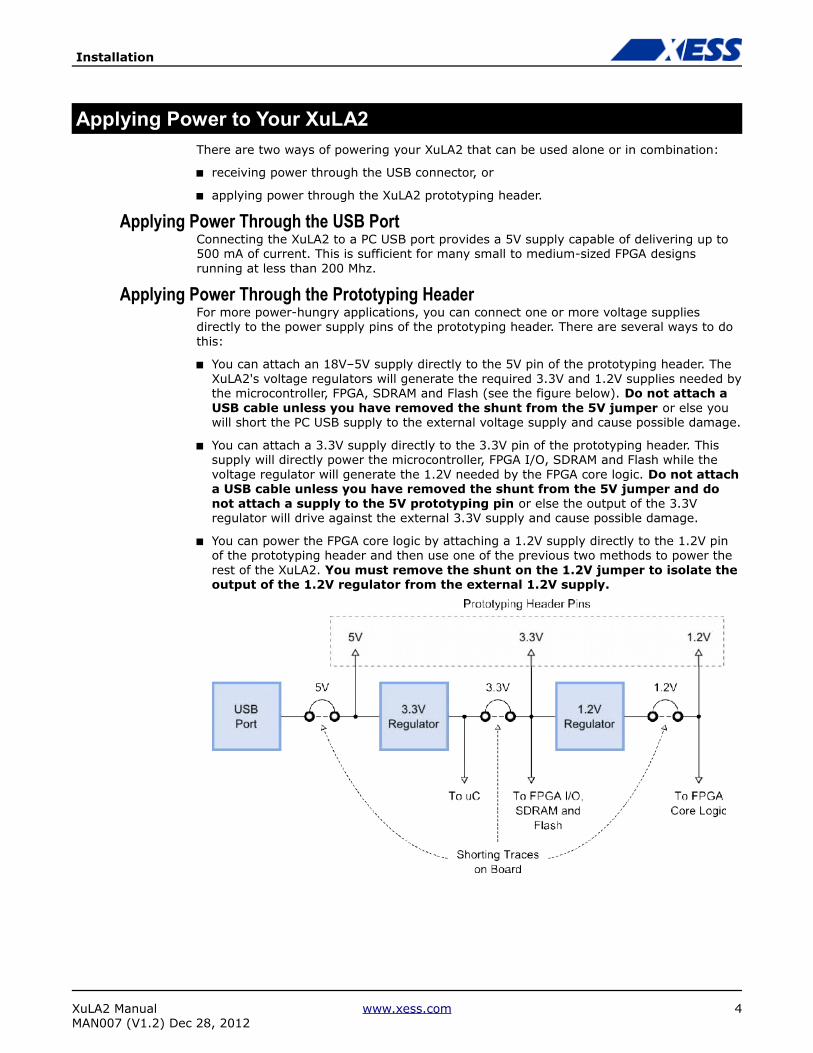
Applying Power Through the Prototyping HeaderFor more power-hungry applications, you can connect one or more voltage supplies directly to the power supply pins of the prototyping header. There are several ways to do this:
You can attach an 18V–5V supply directly to the 5V pin of the prototyping header. The XuLA2's voltage regulators will generate the required 3.3V and 1.2V supplies needed by the microcontroller, FPGA, SDRAM and Flash (see the figure below). Do not attach a USB cable unless you have removed the shunt from the 5V jumper or else you will short the PC USB supply to the external voltage supply and cause possible damage.
You can attach a 3.3V supply directly to the 3.3V pin of the prototyping header. This supply will directly power the microcontroller, FPGA I/O, SDRAM and Flash while the voltage regulator will generate the 1.2V needed by the FPGA core logic. Do not attach a USB cable unless you have removed the shunt from the 5V jumper and do not attach a supply to the 5V prototyping pin or else the output of the 3.3V regulator will drive against the external 3.3V supply and cause possible damage.
You can power the FPGA core logic by attaching a 1.2V supply directly to the 1.2V pin of the prototyping header and then use one of the previous two methods to power the rest of the XuLA2. You must remove the shunt on the 1.2V jumper to isolate the output of the 1.2V regulator from the external 1.2V supply.
XuLA2 Manual www.xess.com 4MAN007 (V1.2) Dec 28, 2012

Installation
Inserting the XuLA2 into a Breadboard
In its factory-original configuration, the XuLA2's prototyping header is empty. If desired, you can solder in a pair of twenty-pin headers and then insert the XuLA2 into a standard solderless breadboard as shown below.
The XuLA2 PCB will accept common headers with 0.025"-thick pins at 0.1" spacing, but you may find it difficult to remove the XuLA2 given how tightly the breadboard grips the pins. A header with thinner pins (such as the Aries 20-0600-20) is a better choice.
XuLA2 Manual www.xess.com 5MAN007 (V1.2) Dec 28, 2012

C.3 ProgrammingThis chapter will show you how to download logic designs into the FPGA of your XuLA2 and how to transfer data between the PC and the SDRAM and Flash memories on the board.
Generating Bitstreams for the FPGA
Before you can download a logic design to the FPGA on your XuLA2, you need to generate a bitstream (i.e., a .BIT file) with XILINX ISE WebPACK. Steps for doing this are given in the XILINX documentation and this XESS tutorial, but there are several details that you have to be aware of when generating the bitstream.
After creating your logic design in ISE WebPACK, right-click on the Generate Programming File item in the Process window and select Process Properties... from the context menu as shown below.
XuLA2 Manual www.xess.com 6MAN007 (V1.2) Dec 28, 2012
Programming
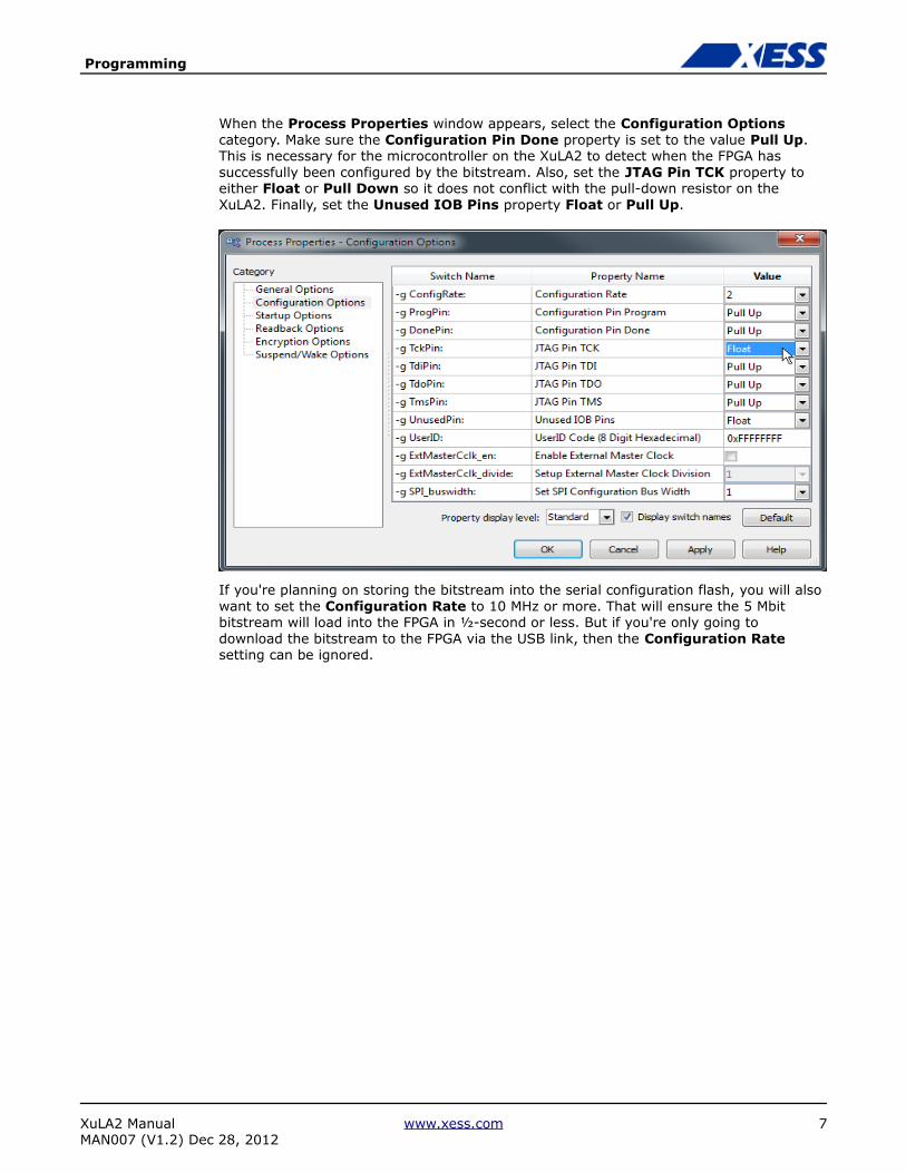
When the Process Properties window appears, select the Configuration Options category. Make sure the Configuration Pin Done property is set to the value Pull Up. This is necessary for the microcontroller on the XuLA2 to detect when the FPGA has successfully been configured by the bitstream. Also, set the JTAG Pin TCK property to either Float or Pull Down so it does not conflict with the pull-down resistor on the XuLA2. Finally, set the Unused IOB Pins property Float or Pull Up.
If you're planning on storing the bitstream into the serial configuration flash, you will also want to set the Configuration Rate to 10 MHz or more. That will ensure the 5 Mbit bitstream will load into the FPGA in ½-second or less. But if you're only going to download the bitstream to the FPGA via the USB link, then the Configuration Rate setting can be ignored.
XuLA2 Manual www.xess.com 7MAN007 (V1.2) Dec 28, 2012

Programming
Finally, select the Startup Options category and set the FPGA Start-Up Clock to one of the following values:
FPGA Start-Up Clock Settings
JTAG Clock Use this setting when your bitstream will be downloaded directly into the XuLA2's FPGA through the USB cable.
CCLK Use this setting when your bitstream will be downloaded into the XuLA2's serial configuration Flash for eventual transfer to the FPGA.
Then click OK to finalize your process properties. Now you're ready to generate a bitstream for the XuLA2!
XuLA2 Manual www.xess.com 8MAN007 (V1.2) Dec 28, 2012

Programming
Downloading Bitstreams into the FPGA
Downloading Using GXSLOADAs you work on a logic design, you will usually download the bitstream from the PC to the XuLA2 to test your modifications. The GXSLOAD utility is used for downloading bitstreams over the USB link.
Start GXSLOAD by double-clicking the icon placed on the desktop during the XSTOOLs installation. This brings up the window shown below.
Now you can download bitstream files to the FPGA or CPLD simply by dragging them from their folder and dropping them into the FPGA/CPLD pane as shown below.
XuLA2 Manual www.xess.com 9MAN007 (V1.2) Dec 28, 2012

Programming
Once you drop the file, the highlighted file name appears in the FPGA/CPLD pane and the Load button is enabled. Clicking on the Load button will begin sending the bitstream to the XuLA2 through the USB cable. GXSLOAD will reject any non-downloadable files (ones with a suffix other than .BIT). During the downloading process, GXSLOAD will display the name of the bitstream file and the progress of the current download. The LED on the XuLA2 will blink as the bitstream is transferred.
You can drag & drop multiple files into the FPGA/CPLD pane. Clicking your mouse on a file name will highlight the name and select it for downloading. Only one file at a time can be selected for downloading.
Double-clicking the highlighted file will deselect it so no file will be downloaded. Doing this disables the Load button.
XuLA2 Manual www.xess.com 10MAN007 (V1.2) Dec 28, 2012

Programming
Downloading Using a XILINX or Third-Party JTAG CableAs an alternative to using GXSLOAD and a simple USB cable, you can use a XILINX or third-party JTAG cable to configure the FPGA on the XuLA2. But first, you have to set a non-volatile flag to give priority to the auxiliary JTAG header using the GXSFLAGS utility. Connect the XuLA to your PC with a USB cable and then double-click the GXSFLAGS icon so the following window appears.
Click on the Enable Aux JTAG checkbox and then click on the Load button to set the flag. Note that the flag only needs to be set once to support the JTAG cable because it retains its value even when power is removed from the XuLA2. (Be aware that enabling the auxiliary JTAG header disables the functions of the other XSTOOLs utilities such as GXSTEST and GXSLOAD. To restore their functions, you'll have to use GXSFLAGS again to disable the auxiliary JTAG header.)
Now attach your JTAG cable to the auxiliary JTAG header as shown below. (The USB cable remains attached only to provide the XuLA2 with power. You can detach it if the board is getting power from another source, such as through its prototyping header.)
XuLA2 Manual www.xess.com 11MAN007 (V1.2) Dec 28, 2012
Programming
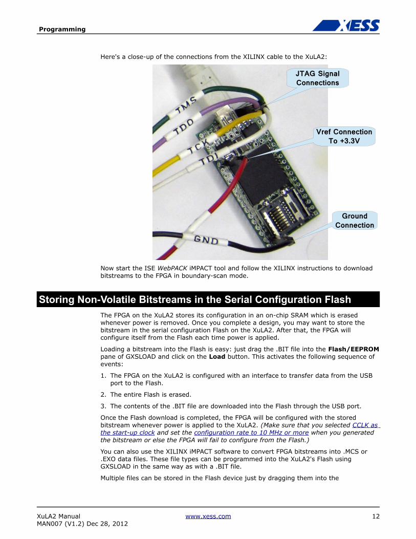
Here's a close-up of the connections from the XILINX cable to the XuLA2:
Now start the ISE WebPACK iMPACT tool and follow the XILINX instructions to download bitstreams to the FPGA in boundary-scan mode.
Storing Non-Volatile Bitstreams in the Serial Configuration Flash
The FPGA on the XuLA2 stores its configuration in an on-chip SRAM which is erased whenever power is removed. Once you complete a design, you may want to store the bitstream in the serial configuration Flash on the XuLA2. After that, the FPGA will configure itself from the Flash each time power is applied.
Loading a bitstream into the Flash is easy: just drag the .BIT file into the Flash/EEPROM pane of GXSLOAD and click on the Load button. This activates the following sequence of events:
1. The FPGA on the XuLA2 is configured with an interface to transfer data from the USB port to the Flash.
2. The entire Flash is erased.
3. The contents of the .BIT file are downloaded into the Flash through the USB port.
Once the Flash download is completed, the FPGA will be configured with the stored bitstream whenever power is applied to the XuLA2. (Make sure that you selected CCLK as the start-up clock and set the configuration rate to 10 MHz or more when you generated the bitstream or else the FPGA will fail to configure from the Flash.)
You can also use the XILINX iMPACT software to convert FPGA bitstreams into .MCS or .EXO data files. These file types can be programmed into the XuLA2's Flash using GXSLOAD in the same way as with a .BIT file.
Multiple files can be stored in the Flash device just by dragging them into the
XuLA2 Manual www.xess.com 12MAN007 (V1.2) Dec 28, 2012
GroundConnection
Vref ConnectionTo +3.3V
JTAG SignalConnections

Programming
Flash/EEPROM area, highlighting the files to be downloaded and clicking the Load button. (Note that anything previously stored in the Flash will be erased by each new download.) This is useful if you need to store information in the Flash in addition to the FPGA bitstream. Files are selected and de-selected for downloading just by clicking on their names in the Flash/EEPROM area. The address ranges of the data in each file should not overlap or this will corrupt the data stored in the Flash device!
You can also examine the contents of the Flash by uploading it to the PC. To upload data from an address range in the Flash, type the upper and lower bounds of the range into the High Address and Low Address fields located below the Flash/EEPROM pane, and select the format for the uploaded data from the Upload Format pulldown list. Then click
on the file icon ( ) and drag & drop it into any folder.
This activates the following sequence of steps:
1. The FPGA on the XuLA2 is configured with an interface between the Flash device and the PC USB port.
2. The Flash data between the high and low addresses (inclusive) is uploaded through the USB port.
3. The uploaded data is stored in a file named FLSHUPLD with an extension that reflects the selected upload file format.
The uploaded data can be stored in the following formats:
MCS: Intel hexadecimal file format.HEX: Identical to MCS format.EXO-16: Motorola S-record format with 16-bit addresses (suitable for 64 KByte
uploads only).EXO-24: Motorola S-record format with 24-bit addresses.EXO-32: Motorola S-record format with 32-bit addresses.XESS-16: XESS hexadecimal format with 16-bit addresses. (This is a simplified file
format that does not use checksums.)
XuLA2 Manual www.xess.com 13MAN007 (V1.2) Dec 28, 2012

Programming
XESS-24: XESS hexadecimal format with 24-bit addresses.XESS-32: XESS hexadecimal format with 32-bit addresses.
Transferring Data to/from the SDRAM
The XuLA2 contains a synchronous DRAM (SDRAM) whose contents can be downloaded and uploaded by GXSLOAD. This is useful for initializing the SDRAM with data for use by the FPGA and then reading the SDRAM contents after the FPGA has operated upon it. The SDRAM is loaded with data by dragging & dropping one or more .EXO, .MCS, .HEX, and/or .XES files into the RAM pane of the gxsload window and then clicking on the Load button. This activates the following sequence of steps:
1. The FPGA is configured with an interface to transfer data between the SDRAM device and the USB port.
2. The contents of the .EXO, .MCS, .HEX or .XES file are downloaded into the SDRAM through the USB port.
You can also examine the contents of the SDRAM device by uploading it to the PC. To upload data from an address range in the SDRAM, type the upper and lower bounds of the range into the High Address and Low Address fields below the RAM pane, and select the format for the uploaded data from the Upload Format pulldown list. Then click
on the file icon ( ) and drag & drop it into any folder.
This activates the following sequence of steps:
1. The FPGA is configured with an interface between the SDRAM device and the PC USB port.
2. The SDRAM data between the high and low addresses (inclusive) is uploaded through the USB port.
3. The uploaded data is stored in a file named RAMUPLD with an extension that reflects the selected upload file format.
XuLA2 Manual www.xess.com 14MAN007 (V1.2) Dec 28, 2012

Programming
The 16-bit data words in the SDRAM are mapped into the eight-bit data format of the .HEX, .MCS, .EXO and .XES files using a Big Endian style. That is, the 16-bit word at location N in the SDRAM is stored in the eight-bit file with the upper eight bits at address 2N and the lower eight bits at address 2N+1. This byte-ordering applies for both RAM uploads and downloads.
XuLA2 Manual www.xess.com 15MAN007 (V1.2) Dec 28, 2012
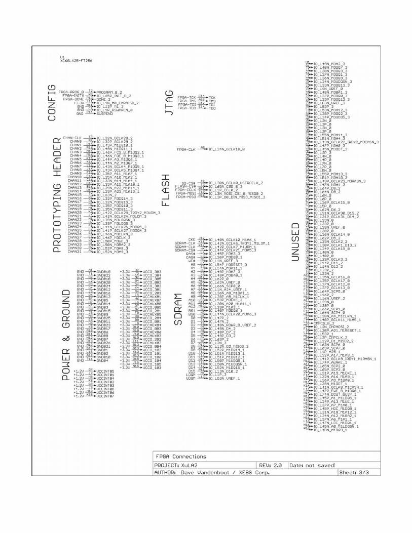
C.4 Programmer ModelsThis section describes the various sections of the XuLA2 and shows how the FPGA I/O is connected to the rest of the circuitry. The schematics which follow are less detailed so as to simplify the descriptions. For more information, you can find a table of pin connections and detailed schematics at the end of this manual.
XuLA2 Components
The XuLA2 contains the following major components:
FPGA: This is the field programmable gate array.Microcontroller: The microcontroller (uC) handles initialization, clock generation
and USB-to-JTAG communications.SDRAM: A 256-Mbit SDRAM provides volatile data storage accessible by
the FPGA.
SPI Flash: An 8-Mbit serial Flash device provides non-volatile storage for FPGA configuration bitstreams and user data.
MicroSD Card: A Secure Digital memory card provides non-volatile storage for user data.
Prototyping Header: FPGA I/O pins, several uC pins and power/GND pins are connected to this 40-pin header that is meant to mate with solderless breadboards or other devices with 0.1"-spacing sockets.
Aux. JTAG Header: This header provides direct access to the FPGA's JTAG pins.
XuLA2 Manual www.xess.com 16MAN007 (V1.2) Dec 28, 2012
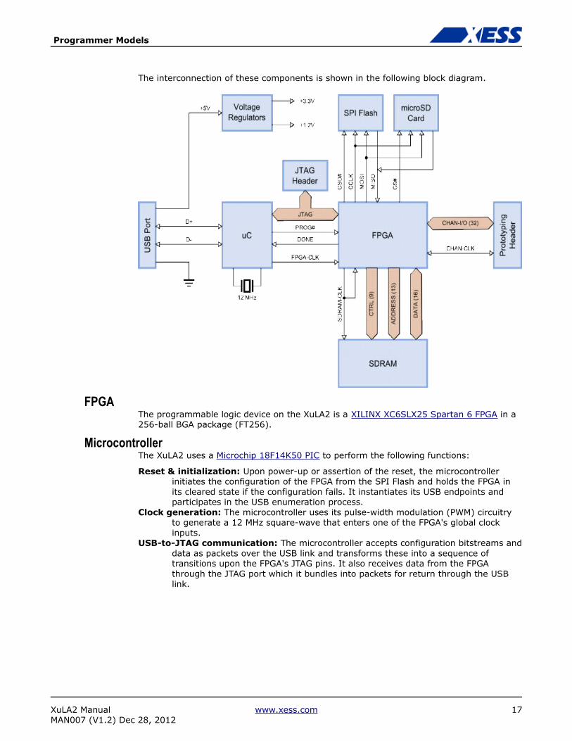
Programmer Models
The interconnection of these components is shown in the following block diagram.
FPGAThe programmable logic device on the XuLA2 is a XILINX XC6SLX25 Spartan 6 FPGA in a 256-ball BGA package (FT256).
MicrocontrollerThe XuLA2 uses a Microchip 18F14K50 PIC to perform the following functions:
Reset & initialization: Upon power-up or assertion of the reset, the microcontroller initiates the configuration of the FPGA from the SPI Flash and holds the FPGA in its cleared state if the configuration fails. It instantiates its USB endpoints and participates in the USB enumeration process.
Clock generation: The microcontroller uses its pulse-width modulation (PWM) circuitry to generate a 12 MHz square-wave that enters one of the FPGA's global clock inputs.
USB-to-JTAG communication: The microcontroller accepts configuration bitstreams and data as packets over the USB link and transforms these into a sequence of transitions upon the FPGA's JTAG pins. It also receives data from the FPGA through the JTAG port which it bundles into packets for return through the USB link.
XuLA2 Manual www.xess.com 17MAN007 (V1.2) Dec 28, 2012

Programmer Models
SDRAMThe XuLA2 incorporates a 16M x 16 SDRAM (Winbond W9825G6JH) that connects to the FPGA as shown below. To compensate for circuit delays, the clock signal to the SDRAM is re-routed back to a global clock input so the FPGA can synchronize itself with the SDRAM.
SPI Flash and microSD CardThe XuLA2 has an 8-Mbit SPI Flash (Winbond W25Q80BV) and a microSD card socket that connect to the FPGA as shown below. During FPGA configuration, the bitstream is read from the SPI flash while the microSD card is disabled. After configuration, either the SPI Flash or the microSD card can be accessed by lowering their respective chip-selects and performing SPI read/write operations.
XuLA2 Manual www.xess.com 18MAN007 (V1.2) Dec 28, 2012

Programmer Models
Prototyping HeaderThe prototyping header connects the FPGA I/O, microcontroller I/O and the power/GND planes to external circuitry. The signals attached to the header pins are shown below.
XuLA2 Header Pin Functions
CHAN0 – CHAN31 These pins connect directly to the FPGA I/O pins. These pins are not 5V-tolerant (see below).
CHAN-CLK This is a direct connection to a global clock pin of the FPGA. It can also be used as a general-purpose I/O pin. This pin is not 5V-tolerant (see below).
+5V, +1.2V, +3.3V, GND
These pins connect to the voltage supply planes of the XuLA2 as depicted in this figure.
RST# This pin connects to the microcontroller reset pin. Pulling it to ground and releasing it will cause the XuLA2 to reconfigure itself.
ANALOG-IO0, ANALOG-IO1
These pins connect to the analog-to-digital converter in the microcontroller. ANALOG-IO0 can also output an analog voltage with a limited range and precision. Both pins are also useable as standard digital I/O pins.
XuLA2 Manual www.xess.com 19MAN007 (V1.2) Dec 28, 2012
Programmer Models
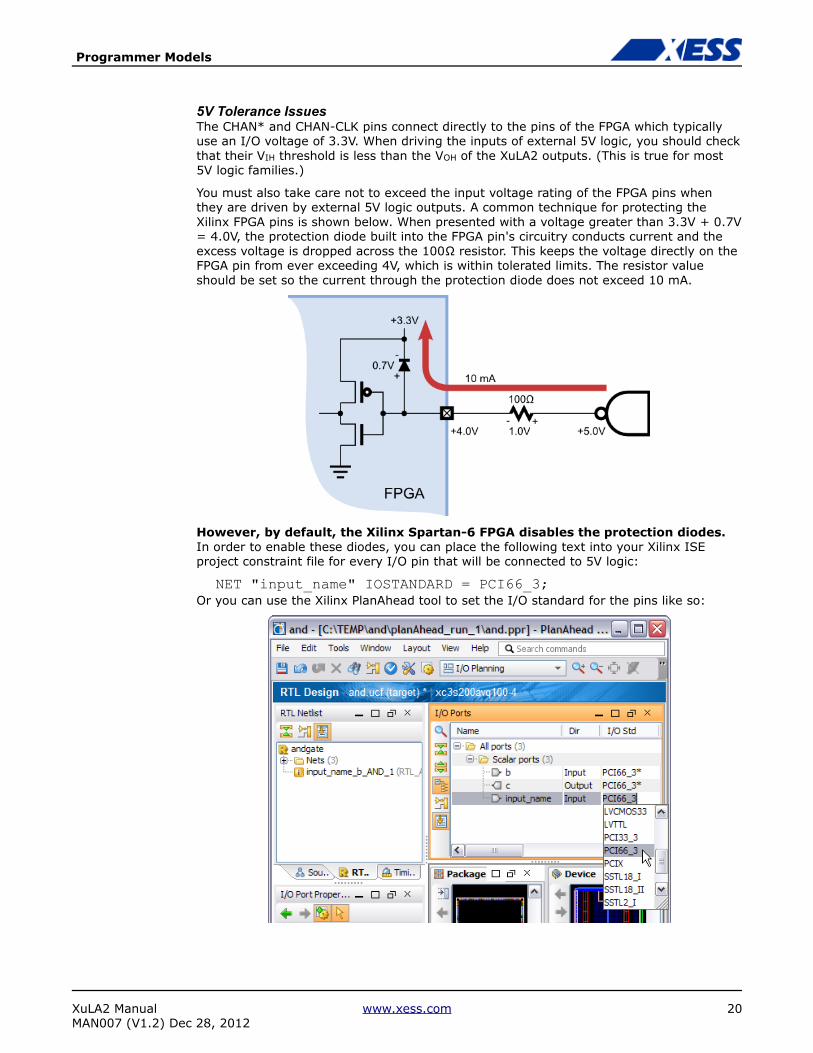
5V Tolerance IssuesThe CHAN* and CHAN-CLK pins connect directly to the pins of the FPGA which typically use an I/O voltage of 3.3V. When driving the inputs of external 5V logic, you should check that their VIH threshold is less than the VOH of the XuLA2 outputs. (This is true for most 5V logic families.)
You must also take care not to exceed the input voltage rating of the FPGA pins when they are driven by external 5V logic outputs. A common technique for protecting the Xilinx FPGA pins is shown below. When presented with a voltage greater than 3.3V + 0.7V = 4.0V, the protection diode built into the FPGA pin's circuitry conducts current and the excess voltage is dropped across the 100Ω resistor. This keeps the voltage directly on the FPGA pin from ever exceeding 4V, which is within tolerated limits. The resistor value should be set so the current through the protection diode does not exceed 10 mA.
However, by default, the Xilinx Spartan-6 FPGA disables the protection diodes. In order to enable these diodes, you can place the following text into your Xilinx ISE project constraint file for every I/O pin that will be connected to 5V logic:
NET "input_name" IOSTANDARD = PCI66_3;Or you can use the Xilinx PlanAhead tool to set the I/O standard for the pins like so:
XuLA2 Manual www.xess.com 20MAN007 (V1.2) Dec 28, 2012
Programmer Models
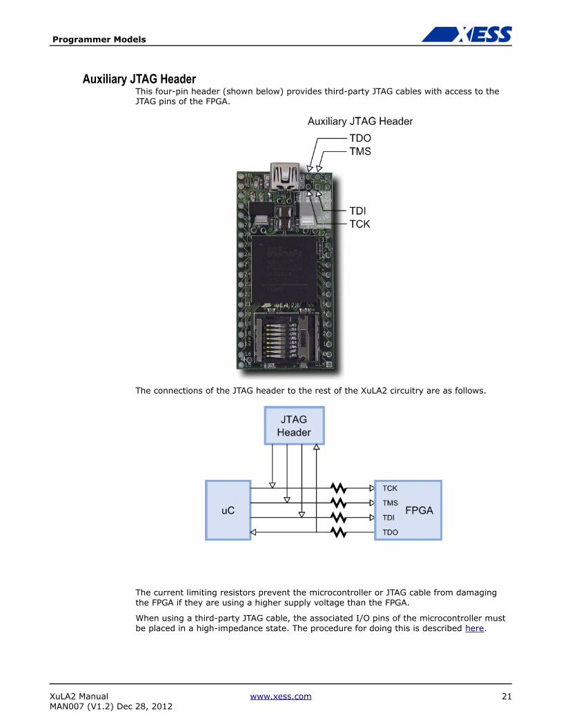
Auxiliary JTAG HeaderThis four-pin header (shown below) provides third-party JTAG cables with access to the JTAG pins of the FPGA.
The connections of the JTAG header to the rest of the XuLA2 circuitry are as follows.
The current limiting resistors prevent the microcontroller or JTAG cable from damaging the FPGA if they are using a higher supply voltage than the FPGA.
When using a third-party JTAG cable, the associated I/O pins of the microcontroller must be placed in a high-impedance state. The procedure for doing this is described here.
XuLA2 Manual www.xess.com 21MAN007 (V1.2) Dec 28, 2012

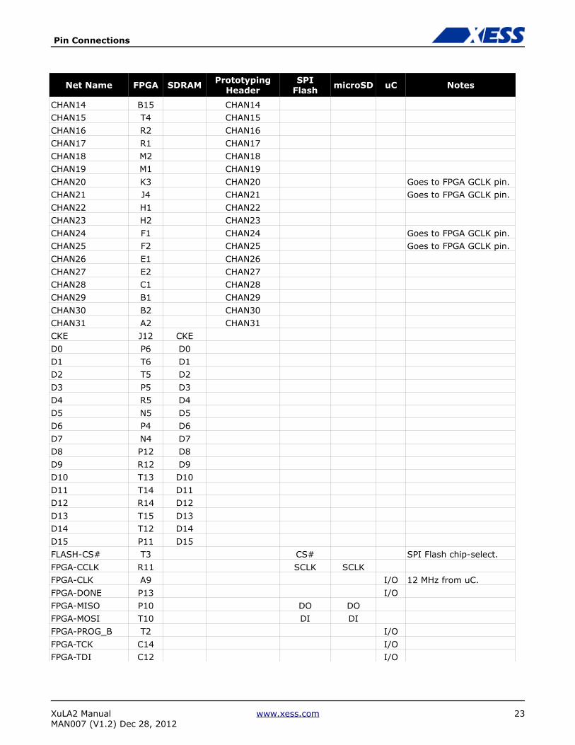
A.1 Pin ConnectionsNet Name FPGA SDRAM Prototyping
HeaderSPI
FlashmicroSD uC Notes
A0 E4 A0A1 E3 A1
A2 D3 A2A3 C3 A3
A4 B12 A4A5 A12 A5
A6 D12 A6A7 E12 A7
A8 G16 A8A9 G12 A9
A10 F4 A10A11 G11 A11
A12 H13 A12BS0 H3 BS0
BS1 G3 BS1CAS# L3 CAS#
CHAN-CLK T7 CHAN-CLK Goes to FPGA GCLK pin.CHAN0 R7 CHAN0 Goes to FPGA GCLK pin.
CHAN1 R15 CHAN1CHAN2 R16 CHAN2
CHAN3 M15 CHAN3CHAN4 M16 CHAN4
CHAN5 K15 CHAN5CHAN6 K16 CHAN6
CHAN7 J16 CHAN7 Goes to FPGA GCLK pin.CHAN8 J14 CHAN8 Goes to FPGA GCLK pin.
CHAN9 F15 CHAN9CHAN10 F16 CHAN10
CHAN11 C16 CHAN11CHAN12 C15 CHAN12
CHAN13 B16 CHAN13
XuLA2 Manual www.xess.com 22MAN007 (V1.2) Dec 28, 2012
Pin Connections
Net Name FPGA SDRAM Prototyping Header
SPIFlash
microSD uC Notes
CHAN14 B15 CHAN14CHAN15 T4 CHAN15
CHAN16 R2 CHAN16CHAN17 R1 CHAN17
CHAN18 M2 CHAN18CHAN19 M1 CHAN19
CHAN20 K3 CHAN20 Goes to FPGA GCLK pin.CHAN21 J4 CHAN21 Goes to FPGA GCLK pin.
CHAN22 H1 CHAN22CHAN23 H2 CHAN23
CHAN24 F1 CHAN24 Goes to FPGA GCLK pin.CHAN25 F2 CHAN25 Goes to FPGA GCLK pin.
CHAN26 E1 CHAN26CHAN27 E2 CHAN27
CHAN28 C1 CHAN28CHAN29 B1 CHAN29
CHAN30 B2 CHAN30CHAN31 A2 CHAN31
CKE J12 CKED0 P6 D0
D1 T6 D1D2 T5 D2
D3 P5 D3D4 R5 D4
D5 N5 D5D6 P4 D6
D7 N4 D7D8 P12 D8
D9 R12 D9D10 T13 D10
D11 T14 D11D12 R14 D12
D13 T15 D13D14 T12 D14
D15 P11 D15FLASH-CS# T3 CS# SPI Flash chip-select.
FPGA-CCLK R11 SCLK SCLKFPGA-CLK A9 I/O 12 MHz from uC.
FPGA-DONE P13 I/OFPGA-MISO P10 DO DO
FPGA-MOSI T10 DI DIFPGA-PROG_B T2 I/O
FPGA-TCK C14 I/OFPGA-TDI C12 I/O
XuLA2 Manual www.xess.com 23MAN007 (V1.2) Dec 28, 2012

Pin Connections
Net Name FPGA SDRAM Prototyping Header
SPIFlash
microSD uC Notes
FPGA-TDO E14 I/OFPGA-TMS A15 I/O
LDQM M4 LDQMRAS# L4 RAS#
SD-CS# T8 CS# MicroSD chip-select.SDRAM-CLK K12 CLK
SDRAM_CLKFB K11 SDRAM clock feedback.SDRAM-CS# H4 CS#
UDQM L13 UDQMWE# M3 WE#
XuLA2 Manual www.xess.com 24MAN007 (V1.2) Dec 28, 2012