Xilinx UG695 ISE In-Depth Tutorial...8 ISE In-Depth Tutorial UG695 (v13.1) March 1, 2011 Chapter 2:...
148
ISE In-Depth Tutorial UG695 (v13.1) March 1, 2011
Transcript of Xilinx UG695 ISE In-Depth Tutorial...8 ISE In-Depth Tutorial UG695 (v13.1) March 1, 2011 Chapter 2:...

ISE In-Depth Tutorial
UG695 (v13.1) March 1, 2011
ISE In-Depth Tutorial www.xilinx.com UG695 (v13.1) March 1, 2011
The information disclosed to you hereunder (the “Information”) is provided “AS-IS” with no warranty of any kind, express or implied. Xilinx does not assume any liability arising from your use of the Information. You are responsible for obtaining any rights you may require for your use of this Information. Xilinx reserves the right to make changes, at any time, to the Information without notice and at its sole discretion. Xilinx assumes no obligation to correct any errors contained in the Information or to advise you of any corrections or updates. Xilinx expressly disclaims any liability in connection with technical support or assistance that may be provided to you in connection with the Information. XILINX MAKES NO OTHER WARRANTIES, WHETHER EXPRESS, IMPLIED, OR STATUTORY, REGARDING THE INFORMATION, INCLUDING ANY WARRANTIES OF MERCHANTABILITY, FITNESS FOR A PARTICULAR PURPOSE, OR NONINFRINGEMENT OF THIRD-PARTY RIGHTS.
© Copyright 2011 Xilinx, Inc. XILINX, the Xilinx logo, Virtex, Spartan, ISE, and other designated brands included herein are trademarks of Xilinx in the United States and other countries. All other trademarks are the property of their respective owners.
Revision HistoryThe following table shows the revision history for this document.
Date Version Revision
03/01/11 13.1 • Changed tutorial directory to: c:\xilinx_tutorial• Updated CORE Generator software graphics.• Updated third party synthesis tool versions.
ISE In-Depth Tutorial www.xilinx.com 3UG695 (v13.1) March 1, 2011
Revision History . . . . . . . . . . . . . . . . . . . . . . . . . . . . . . . . . . . . . . . . . . . . . . . . . . . . . . . . . . . . . 2
Chapter 1: IntroductionAbout the In-Depth Tutorial . . . . . . . . . . . . . . . . . . . . . . . . . . . . . . . . . . . . . . . . . . . . . . . . . 5Tutorial Contents . . . . . . . . . . . . . . . . . . . . . . . . . . . . . . . . . . . . . . . . . . . . . . . . . . . . . . . . . . . . 5Tutorial Flows . . . . . . . . . . . . . . . . . . . . . . . . . . . . . . . . . . . . . . . . . . . . . . . . . . . . . . . . . . . . . . . 6
Chapter 2: Overview of ISE SoftwareSoftware Overview. . . . . . . . . . . . . . . . . . . . . . . . . . . . . . . . . . . . . . . . . . . . . . . . . . . . . . . . . . . 7Using Project Revision Management Features . . . . . . . . . . . . . . . . . . . . . . . . . . . . . . . 11
Chapter 3: HDL-Based DesignOverview of HDL-Based Design. . . . . . . . . . . . . . . . . . . . . . . . . . . . . . . . . . . . . . . . . . . . . 13Getting Started. . . . . . . . . . . . . . . . . . . . . . . . . . . . . . . . . . . . . . . . . . . . . . . . . . . . . . . . . . . . . . 13Design Description . . . . . . . . . . . . . . . . . . . . . . . . . . . . . . . . . . . . . . . . . . . . . . . . . . . . . . . . . 17Design Entry . . . . . . . . . . . . . . . . . . . . . . . . . . . . . . . . . . . . . . . . . . . . . . . . . . . . . . . . . . . . . . . . 18Synthesizing the Design . . . . . . . . . . . . . . . . . . . . . . . . . . . . . . . . . . . . . . . . . . . . . . . . . . . . 33
Chapter 4: Schematic-Based DesignOverview of Schematic-Based Design . . . . . . . . . . . . . . . . . . . . . . . . . . . . . . . . . . . . . . . 41Getting Started. . . . . . . . . . . . . . . . . . . . . . . . . . . . . . . . . . . . . . . . . . . . . . . . . . . . . . . . . . . . . . 41Design Description . . . . . . . . . . . . . . . . . . . . . . . . . . . . . . . . . . . . . . . . . . . . . . . . . . . . . . . . . 43Design Entry . . . . . . . . . . . . . . . . . . . . . . . . . . . . . . . . . . . . . . . . . . . . . . . . . . . . . . . . . . . . . . . . 46
Chapter 5: Behavioral SimulationOverview of Behavioral Simulation Flow . . . . . . . . . . . . . . . . . . . . . . . . . . . . . . . . . . . . 75ModelSim Setup . . . . . . . . . . . . . . . . . . . . . . . . . . . . . . . . . . . . . . . . . . . . . . . . . . . . . . . . . . . . 75ISim Setup . . . . . . . . . . . . . . . . . . . . . . . . . . . . . . . . . . . . . . . . . . . . . . . . . . . . . . . . . . . . . . . . . . 75Getting Started. . . . . . . . . . . . . . . . . . . . . . . . . . . . . . . . . . . . . . . . . . . . . . . . . . . . . . . . . . . . . . 76Adding an HDL Test Bench . . . . . . . . . . . . . . . . . . . . . . . . . . . . . . . . . . . . . . . . . . . . . . . . . 78Behavioral Simulation Using ModelSim . . . . . . . . . . . . . . . . . . . . . . . . . . . . . . . . . . . . . 79Behavioral Simulation Using ISim . . . . . . . . . . . . . . . . . . . . . . . . . . . . . . . . . . . . . . . . . . 85
Chapter 6: Design ImplementationOverview of Design Implementation . . . . . . . . . . . . . . . . . . . . . . . . . . . . . . . . . . . . . . . . 91Getting Started. . . . . . . . . . . . . . . . . . . . . . . . . . . . . . . . . . . . . . . . . . . . . . . . . . . . . . . . . . . . . . 91Specifying Options . . . . . . . . . . . . . . . . . . . . . . . . . . . . . . . . . . . . . . . . . . . . . . . . . . . . . . . . . 93Creating Timing Constraints . . . . . . . . . . . . . . . . . . . . . . . . . . . . . . . . . . . . . . . . . . . . . . . . 94
Table of Contents
4 www.xilinx.com ISE In-Depth TutorialUG695 (v13.1) March 1, 2011
Translating the Design . . . . . . . . . . . . . . . . . . . . . . . . . . . . . . . . . . . . . . . . . . . . . . . . . . . . . . 94Using the Constraints Editor . . . . . . . . . . . . . . . . . . . . . . . . . . . . . . . . . . . . . . . . . . . . . . . . 95Assigning I/O Locations Using PlanAhead Software . . . . . . . . . . . . . . . . . . . . . . . . 101Mapping the Design . . . . . . . . . . . . . . . . . . . . . . . . . . . . . . . . . . . . . . . . . . . . . . . . . . . . . . . 104Using Timing Analysis to Evaluate Block Delays After Mapping. . . . . . . . . . . . 106Placing and Routing the Design . . . . . . . . . . . . . . . . . . . . . . . . . . . . . . . . . . . . . . . . . . . . 108Using FPGA Editor to Verify the Place and Route . . . . . . . . . . . . . . . . . . . . . . . . . . . 109Evaluating Post-Layout Timing . . . . . . . . . . . . . . . . . . . . . . . . . . . . . . . . . . . . . . . . . . . . . 111Creating Configuration Data . . . . . . . . . . . . . . . . . . . . . . . . . . . . . . . . . . . . . . . . . . . . . . . 113Command Line Implementation . . . . . . . . . . . . . . . . . . . . . . . . . . . . . . . . . . . . . . . . . . . . 116
Chapter 7: Timing SimulationOverview of Timing Simulation Flow . . . . . . . . . . . . . . . . . . . . . . . . . . . . . . . . . . . . . . 117Getting Started. . . . . . . . . . . . . . . . . . . . . . . . . . . . . . . . . . . . . . . . . . . . . . . . . . . . . . . . . . . . . 117Timing Simulation Using ModelSim . . . . . . . . . . . . . . . . . . . . . . . . . . . . . . . . . . . . . . . 118Timing Simulation Using Xilinx ISim . . . . . . . . . . . . . . . . . . . . . . . . . . . . . . . . . . . . . . 126
Chapter 8: Configuration Using iMPACTOverview of iMPACT . . . . . . . . . . . . . . . . . . . . . . . . . . . . . . . . . . . . . . . . . . . . . . . . . . . . . . 131Device Support . . . . . . . . . . . . . . . . . . . . . . . . . . . . . . . . . . . . . . . . . . . . . . . . . . . . . . . . . . . . 131Download Cable Support . . . . . . . . . . . . . . . . . . . . . . . . . . . . . . . . . . . . . . . . . . . . . . . . . . 131Configuration Mode Support . . . . . . . . . . . . . . . . . . . . . . . . . . . . . . . . . . . . . . . . . . . . . . . 131Getting Started. . . . . . . . . . . . . . . . . . . . . . . . . . . . . . . . . . . . . . . . . . . . . . . . . . . . . . . . . . . . . 132Using Boundary-Scan Configuration Mode . . . . . . . . . . . . . . . . . . . . . . . . . . . . . . . . . 133Troubleshooting Boundary-Scan Configuration . . . . . . . . . . . . . . . . . . . . . . . . . . . . 140Creating an SVF File . . . . . . . . . . . . . . . . . . . . . . . . . . . . . . . . . . . . . . . . . . . . . . . . . . . . . . . 141
Appendix A: Additional ResourcesXilinx Resources . . . . . . . . . . . . . . . . . . . . . . . . . . . . . . . . . . . . . . . . . . . . . . . . . . . . . . . . . . . 147ISE Documentation . . . . . . . . . . . . . . . . . . . . . . . . . . . . . . . . . . . . . . . . . . . . . . . . . . . . . . . . 147
ISE In-Depth Tutorial www.xilinx.com 5UG695 (v13.1) March 1, 2011
Chapter 1
Introduction
About the In-Depth TutorialThis tutorial gives a description of the features and additions to the Xilinx® ISE® Design Suite. The primary focus of this tutorial is to show the relationship among the design entry tools, Xilinx and third-party tools, and the design implementation tools.
This guide is a learning tool for designers who are unfamiliar with the features of the ISE software or those wanting to refresh their skills and knowledge.
You may choose to follow one of the three tutorial flows available in this document. For information about the tutorial flows, see Tutorial Flows.
Tutorial ContentsThis guide covers the following topics:
• Chapter 2, Overview of ISE Software, introduces you to the primary user interface for the ISE software, Project Navigator, and the synthesis tools available for your design.
• Chapter 3, HDL-Based Design, guides you through a typical HDL-based design procedure using a design of a runner’s stopwatch. This chapter also shows how to use ISE software accessories, such as the CORE Generator™ software and ISE Text Editor.
• Chapter 4, Schematic-Based Design, explains many different facets of a schematic-based ISE software design flow using a design of a runner’s stopwatch. This chapter also shows how to use ISE software accessories, such as the CORE Generator software and ISE Text Editor.
• Chapter 5, Behavioral Simulation, explains how to simulate a design before design implementation to verify that the logic that you have created is correct.
• Chapter 6, Design Implementation, describes how to Translate, Map, Place, Route, and generate a bitstream file for designs.
• Chapter 7, Timing Simulation, explains how to perform a timing simulation using the block and routing delay information from the routed design to give an accurate assessment of the behavior of the circuit under worst-case conditions.
• Chapter 8, Configuration Using iMPACT, explains how to program a device with a newly created design using the IMPACT configuration tool.
6 www.xilinx.com ISE In-Depth TutorialUG695 (v13.1) March 1, 2011
Chapter 1: Introduction
Tutorial FlowsThis document contains three tutorial flows. In this section, the three tutorial flows are outlined and briefly described to help you determine which sequence of chapters applies to your needs. The tutorial flows include the following:
• HDL design flow
• Schematic design flow
• Implementation-only flow
HDL Design FlowThe HDL design flow is as follows:
1. Chapter 3, HDL-Based Design
2. Chapter 5, Behavioral Simulation
Note: Although behavioral simulation is optional, it is strongly recommended in this tutorial flow.
3. Chapter 6, Design Implementation
4. Chapter 7, Timing Simulation
Note: Although timing simulation is optional, it is strongly recommended in this tutorial flow.
5. Chapter 8, Configuration Using iMPACT
Schematic Design FlowThe schematic design flow is as follows:
1. Chapter 4, Schematic-Based Design
2. Chapter 5, Behavioral Simulation
Note: Although behavioral simulation is optional, it is strongly recommended in this tutorial flow.
3. Chapter 6, Design Implementation
4. Chapter 7, Timing Simulation
Note: Although timing simulation is optional, it is strongly recommended in this tutorial flow.
5. Chapter 8, Configuration Using iMPACT
Implementation-Only FlowThe implementation-only flow is as follows:
1. Chapter 6, Design Implementation
2. Chapter 7, Timing Simulation
Note: Although timing simulation is optional, it is strongly recommended in this tutorial flow.
3. Chapter 8, Configuration Using iMPACT
ISE In-Depth Tutorial www.xilinx.com 7UG695 (v13.1) March 1, 2011
Chapter 2
Overview of ISE Software
Software OverviewThe ISE® software controls all aspects of the design flow. Through the Project Navigator interface, you can access all of the design entry and design implementation tools. You can also access the files and documents associated with your project.
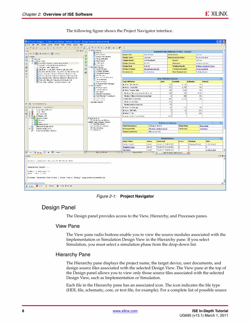
Project Navigator InterfaceBy default, the Project Navigator interface is divided into four panel sub-windows, as seen in Figure 2-1. On the top left are the Start, Design, Files, and Libraries panels, which include display and access to the source files in the project as well as access to running processes for the currently selected source. The Start panel provides quick access to opening projects as well as frequently access reference material, documentation and tutorials. At the bottom of the Project Navigator are the Console, Errors, and Warnings panels, which display status messages, errors, and warnings. To the right is a multi-document interface (MDI) window referred to as the Workspace. The Workspace enables you to view design reports, text files, schematics, and simulation waveforms. Each window can be resized, undocked from Project Navigator, moved to a new location within the main Project Navigator window, tiled, layered, or closed. You can use the View > Panels menu commands to open or close panels. You can use the Layout > Load Default Layout to restore the default window layout. These windows are discussed in more detail in the following sections.
8 www.xilinx.com ISE In-Depth TutorialUG695 (v13.1) March 1, 2011
Chapter 2: Overview of ISE Software
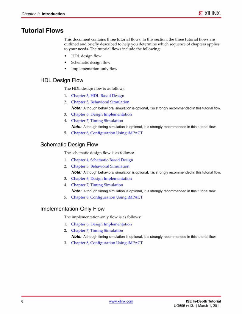
The following figure shows the Project Navigator interface.
Design PanelThe Design panel provides access to the View, Hierarchy, and Processes panes.
View Pane
The View pane radio buttons enable you to view the source modules associated with the Implementation or Simulation Design View in the Hierarchy pane. If you select Simulation, you must select a simulation phase from the drop-down list.
Hierarchy Pane
The Hierarchy pane displays the project name, the target device, user documents, and design source files associated with the selected Design View. The View pane at the top of the Design panel allows you to view only those source files associated with the selected Design View, such as Implementation or Simulation.
Each file in the Hierarchy pane has an associated icon. The icon indicates the file type (HDL file, schematic, core, or text file, for example). For a complete list of possible source
X-Ref Target - Figure 2-1
Figure 2-1: Project Navigator
ISE In-Depth Tutorial www.xilinx.com 9UG695 (v13.1) March 1, 2011
Software Overview
types and their associated icons, see the “Source File Types” topic in the ISE Help. From Project Navigator, select Help > Help Topics to view the ISE Help.
If a file contains lower levels of hierarchy, the icon has a plus symbol (+) to the left of the name. You can expand the hierarchy by clicking the plus symbol (+). You can open a file for editing by double-clicking on the filename.
Processes Pane
The Processes pane is context sensitive, and it changes based upon the source type selected in the Sources pane and the top-level source in your project. From the Processes pane, you can run the functions necessary to define, run, and analyze your design. The Processes pane provides access to the following functions:
• Design Summary/Reports
Provides access to design reports, messages, and summary of results data. Message filtering can also be performed.
• Design Utilities
Provides access to symbol generation, instantiation templates, viewing command line history, and simulation library compilation.
• User Constraints
Provides access to editing location and timing constraints.
• Synthesis
Provides access to Check Syntax, Synthesis, View RTL or Technology Schematic, and synthesis reports. Available processes vary depending on the synthesis tools you use.
• Implement Design
Provides access to implementation tools and post-implementation analysis tools.
• Generate Programming File
Provides access to bitstream generation.
• Configure Target Device
Provides access to configuration tools for creating programming files and programming the device.
The Processes pane incorporates dependency management technology. The tools keep track of which processes have been run and which processes need to be run. Graphical status indicators display the state of the flow at any given time. When you select a process in the flow, the software automatically runs the processes necessary to get to the desired step. For example, when you run the Implement Design process, Project Navigator also runs the Synthesis process because implementation is dependent on up-to-date synthesis results.
To view a running log of command line arguments used on the current project, expand Design Utilities and select View Command Line Log File. See Command Line Implementation in Chapter 6 for further details.
Files PanelThe Files panel provides a flat, sortable list of all the source files in the project. Files can be sorted by any of the columns in the view. Properties for each file can be viewed and modified by right-clicking on the file and selecting Source Properties.
10 www.xilinx.com ISE In-Depth TutorialUG695 (v13.1) March 1, 2011
Chapter 2: Overview of ISE Software
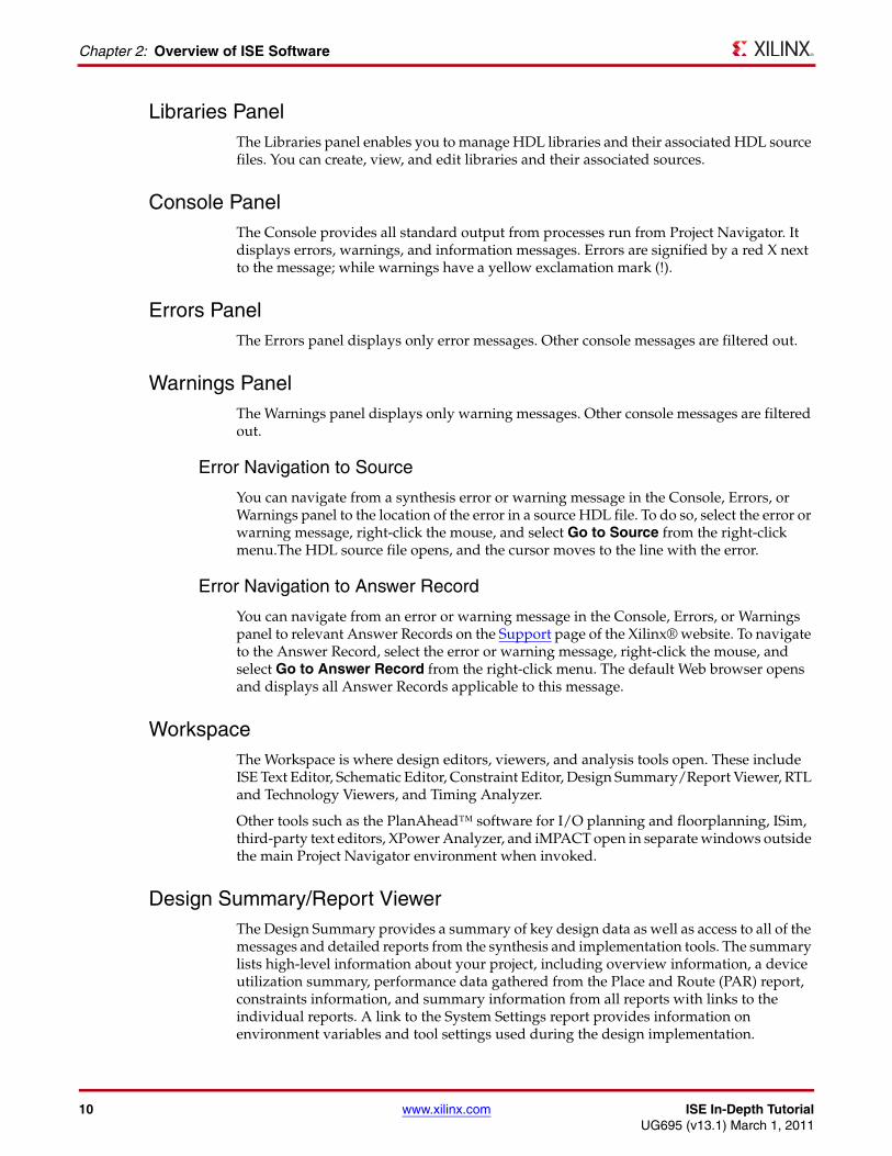
Libraries PanelThe Libraries panel enables you to manage HDL libraries and their associated HDL source files. You can create, view, and edit libraries and their associated sources.
Console PanelThe Console provides all standard output from processes run from Project Navigator. It displays errors, warnings, and information messages. Errors are signified by a red X next to the message; while warnings have a yellow exclamation mark (!).
Errors PanelThe Errors panel displays only error messages. Other console messages are filtered out.
Warnings PanelThe Warnings panel displays only warning messages. Other console messages are filtered out.
Error Navigation to Source
You can navigate from a synthesis error or warning message in the Console, Errors, or Warnings panel to the location of the error in a source HDL file. To do so, select the error or warning message, right-click the mouse, and select Go to Source from the right-click menu.The HDL source file opens, and the cursor moves to the line with the error.
Error Navigation to Answer Record
You can navigate from an error or warning message in the Console, Errors, or Warnings panel to relevant Answer Records on the Support page of the Xilinx® website. To navigate to the Answer Record, select the error or warning message, right-click the mouse, and select Go to Answer Record from the right-click menu. The default Web browser opens and displays all Answer Records applicable to this message.
WorkspaceThe Workspace is where design editors, viewers, and analysis tools open. These include ISE Text Editor, Schematic Editor, Constraint Editor, Design Summary/Report Viewer, RTL and Technology Viewers, and Timing Analyzer.
Other tools such as the PlanAhead™ software for I/O planning and floorplanning, ISim, third-party text editors, XPower Analyzer, and iMPACT open in separate windows outside the main Project Navigator environment when invoked.
Design Summary/Report ViewerThe Design Summary provides a summary of key design data as well as access to all of the messages and detailed reports from the synthesis and implementation tools. The summary lists high-level information about your project, including overview information, a device utilization summary, performance data gathered from the Place and Route (PAR) report, constraints information, and summary information from all reports with links to the individual reports. A link to the System Settings report provides information on environment variables and tool settings used during the design implementation.
ISE In-Depth Tutorial www.xilinx.com 11UG695 (v13.1) March 1, 2011
Using Project Revision Management Features
Messaging features such as message filtering, tagging, and incremental messaging are also available from this view.
Using Project Revision Management FeaturesProject Navigator enables you to manage your project as follows.
Understanding the ISE Project FileThe ISE project file (.xise extension) is an XML file that contains all source-relevant data for the project as follows:
• ISE software version information
• List of source files contained in the project
• Source settings, including design and process properties
The ISE project file does not contain the following:
• Process status information
• Command history
• Constraints data
Note: A .gise file also exists, which contains generated data, such as process status. You should not need to directly interact with this file.
The ISE project file includes the following characteristics, which are compatible with source control environments:
• Contains all of the necessary source settings and input data for the project.
• Can be opened in Project Navigator in a read-only state.
• Only updated or modified if a source-level change is made to the project.
• Can be kept in a directory separate from the generated output directory (working directory).
Note: A source-level change is a change to a property or the addition or removal of a source file. Changes to the contents of a source file or changes to the state of an implementation run are not considered source-level changes and do not result in an update to the project file.
Making a Copy of a ProjectYou can create a copy of a project using File > Copy Project to experiment with different source options and implementations. Depending on your needs, the design source files for the copied project and their location can vary as follows:
• Design source files can be left in their existing location, and the copied project points to these files.
• Design source files, including generated files, can be copied and placed in a specified directory.
• Design source files, excluding generated files, can be copied and placed in a specified directory.
12 www.xilinx.com ISE In-Depth TutorialUG695 (v13.1) March 1, 2011
Chapter 2: Overview of ISE Software
Using the Project BrowserThe Project Browser, accessible by selecting File > Project Browser, provides a convenient way to compare, view, and open projects as follows:
• Compare key characteristics between multiple projects.
• View Design Summary and Reports for a selected project before opening the full project.
• Compare detailed information for two selected projects.
• Open a selected project in the current Project Navigator session.
• Open a selected project in a new Project Navigator session.
Using Project ArchivesYou can also archive the entire project into a single compressed file. This allows for easier transfer over email and storage of numerous projects in a limited space.
Creating an Archive
To create an archive, do the following:
1. Select Project > Archive.
2. In the Project Archive dialog box, enter the archive name and location.
3. Click Save.
Note: The archive contains all of the files in the project directory along with project settings. Remote sources are included in the archive under a folder named remote_sources. For more information, see the ISE Help.
Restoring an Archive
You cannot restore an archived file directly into Project Navigator. The compressed file can be extracted with any ZIP utility, and you can then open the extracted file in Project Navigator.
ISE In-Depth Tutorial www.xilinx.com 13UG695 (v13.1) March 1, 2011
Chapter 3
HDL-Based Design
Overview of HDL-Based DesignThis chapter guides you through a typical HDL-based design procedure using a design of a runner’s stopwatch. The design example used in this tutorial demonstrates many device features, software features, and design flow practices you can apply to your own design. This design targets a Spartan™-3A device; however, all of the principles and flows taught are applicable to any Xilinx® device family, unless otherwise noted.
The design is composed of HDL elements and two cores. You can synthesize the design using Xilinx Synthesis Technology (XST), Synplify/Synplify Pro, or Precision software.
This chapter is the first chapter in the HDL Design Flow. After the design is successfully defined, you will perform behavioral simulation (Chapter 5, Behavioral Simulation), run implementation with the Xilinx implementation tools (Chapter 6, Design Implementation), perform timing simulation (Chapter 7, Timing Simulation), and configure and download to the Spartan-3A device (XC3S700A) demo board (Chapter 8, Configuration Using iMPACT).
Getting StartedThe following sections describe the basic requirements for running the tutorial.
Required SoftwareTo perform this tutorial, you must have Xilinx ISE® Design Suite installed.
This tutorial assumes that the software is installed in the default location c:\xilinx\release_number\ISE_DS\ISE. If you installed the software in a different location, substitute your installation path in the procedures that follow.
Note: For detailed software installation instructions, refer to the ISE Design Suite: Installation and Licensing Guide (UG798) available from the Xilinx website.
Optional Software RequirementsThe following third-party synthesis tools are incorporated into this tutorial and may be used in place of Xilinx Synthesis Technology (XST):
• Synopsys Synplify/Synplify Pro D-2010.06 (or above)
• Mentor Precision Synthesis 2010a (or above)
14 www.xilinx.com ISE In-Depth TutorialUG695 (v13.1) March 1, 2011
Chapter 3: HDL-Based Design
The following third-party simulation tool is optional for this tutorial and may be used in place of ISim:
• ModelSim SE/PE/DE 6.6d (or above)
VHDL or VerilogThis tutorial supports both VHDL and Verilog designs and applies to both designs simultaneously, noting differences where applicable. You will need to decide which HDL language you would like to work through for the tutorial and download the appropriate files for that language. XST can synthesize a mixed-language design. However, this tutorial does not cover the mixed language feature.
Installing the Tutorial Project FilesThe tutorial project files are provided with the ISE Design Suite Tutorials available from the Xilinx website. Download either the VHDL or the Verilog design flow project files.
After you have downloaded the tutorial project files from the web, unzip the tutorial projects into the c:\xilinx_tutorial directory, replacing any existing files in that directory.
When you unzip the tutorial project files into c:\xilinx_tutorial, the directory wtut_vhd (for a VHDL design flow) or wtut_ver (for a Verilog design flow) is created within c:\xilinx_tutorial, and the tutorial files are copied into the newly-created directory.
The following table lists the locations of tutorial source files.
Note: The completed directories contain the finished HDL source files. Do not overwrite any files in the completed directories.
This tutorial assumes that the files are unzipped under c:\xilinx_tutorial, but you can unzip the source files into any directory with read/write permissions. If you unzip the files into a different location, substitute your project path in the procedures that follow.
Starting the ISE SoftwareTo start the ISE software, double-click the ISE Project Navigator icon on your desktop, or select Start > All Programs > Xilinx ISE Design Suite > ISE Design Tools > Project Navigator.
Table 3-1: Tutorial Directories
Directory Description
wtut_vhd Incomplete VHDL Source Files
wtut_ver Incomplete Verilog Source Files
wtut_vhd\wtut_vhd_completed Completed VHDL Source Files
wtut_ver\wtut_ver_completed Completed Verilog Source Files
X-Ref Target - Figure 3-1
Figure 3-1: Project Navigator Desktop Icon
ISE In-Depth Tutorial www.xilinx.com 15UG695 (v13.1) March 1, 2011
Getting Started
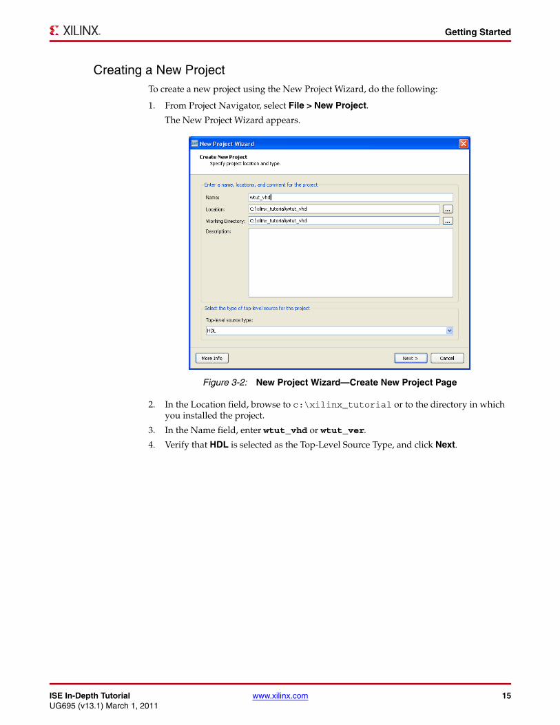
Creating a New ProjectTo create a new project using the New Project Wizard, do the following:
1. From Project Navigator, select File > New Project.
The New Project Wizard appears.
2. In the Location field, browse to c:\xilinx_tutorial or to the directory in which you installed the project.
3. In the Name field, enter wtut_vhd or wtut_ver.
4. Verify that HDL is selected as the Top-Level Source Type, and click Next.
X-Ref Target - Figure 3-2
Figure 3-2: New Project Wizard—Create New Project Page
16 www.xilinx.com ISE In-Depth TutorialUG695 (v13.1) March 1, 2011
Chapter 3: HDL-Based Design
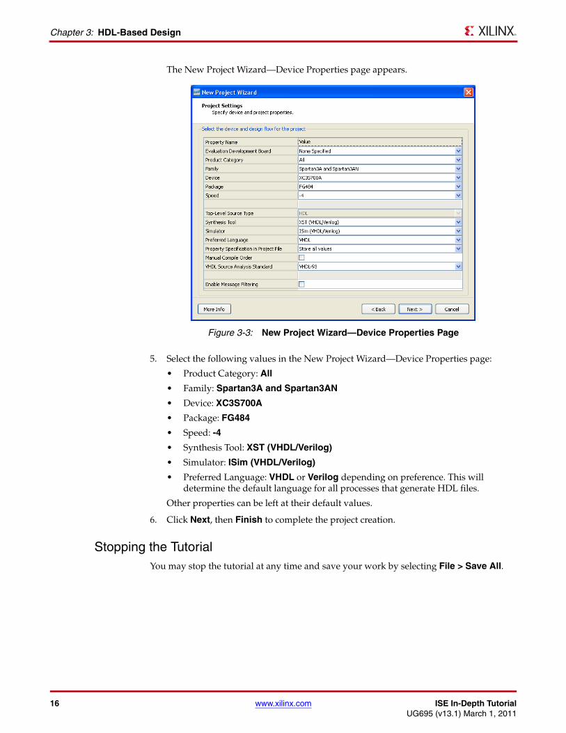
The New Project Wizard—Device Properties page appears.
5. Select the following values in the New Project Wizard—Device Properties page:
• Product Category: All
• Family: Spartan3A and Spartan3AN
• Device: XC3S700A
• Package: FG484
• Speed: -4
• Synthesis Tool: XST (VHDL/Verilog)
• Simulator: ISim (VHDL/Verilog)
• Preferred Language: VHDL or Verilog depending on preference. This will determine the default language for all processes that generate HDL files.
Other properties can be left at their default values.
6. Click Next, then Finish to complete the project creation.
Stopping the TutorialYou may stop the tutorial at any time and save your work by selecting File > Save All.
X-Ref Target - Figure 3-3
Figure 3-3: New Project Wizard—Device Properties Page

ISE In-Depth Tutorial www.xilinx.com 17UG695 (v13.1) March 1, 2011
Design Description
Design DescriptionThe design used in this tutorial is a hierarchical, HDL-based design, which means that the top-level design file is an HDL file that references several other lower-level macros. The lower-level macros are either HDL modules or IP modules.
The design begins as an unfinished design. Throughout the tutorial, you will complete the design by generating some of the modules from scratch and by completing others from existing files. When the design is complete, you will simulate it to verify the design functionality.
In the runner’s stopwatch design, there are five external inputs and four external output buses. The system clock is an externally generated signal. The following list summarizes the input and output signals of the design.
InputsThe following are input signals for the tutorial stopwatch design:
• strtstop
Starts and stops the stopwatch. This is an active low signal which acts like the start/stop button on a runner’s stopwatch.
• reset
Puts the stopwatch in clocking mode and resets the time to 0:00:00.
• clk
Externally generated system clock.
• mode
Toggles between clocking and timer modes. This input is only functional while the clock or timer is not counting.
• lap_load
This is a dual function signal. In clocking mode, it displays the current clock value in the ‘Lap’ display area. In timer mode, it loads the pre-assigned values from the ROM to the timer display when the timer is not counting.
OutputsThe following are outputs signals for the design:
• lcd_e, lcd_rs, lcd_rw
These outputs are the control signals for the LCD display of the Spartan-3A demo board used to display the stopwatch times.
• sf_d[7:0]
Provides the data values for the LCD display.
Functional BlocksThe completed design consists of the following functional blocks:
• clk_div_262k
Macro that divides a clock frequency by 262,144. Converts 26.2144 MHz clock into 100 Hz 50% duty cycle clock.
18 www.xilinx.com ISE In-Depth TutorialUG695 (v13.1) March 1, 2011
Chapter 3: HDL-Based Design
• dcm1
Clocking Wizard macro with internal feedback, frequency controlled output, and duty-cycle correction. The CLKFX_OUT output converts the 50 MHz clock of the Spartan-3A demo board to 26.2144 MHz.
• debounce
Schematic module implementing a simplistic debounce circuit for the strtstop, mode, and lap_load input signals.
• lcd_control
Module controlling the initialization of and output to the LCD display.
• statmach
State machine HDL module that controls the state of the stopwatch.
• timer_preset
CORE Generator™ software 64x20 ROM. This macro contains 64 preset times from 0:00:00 to 9:59:99 that can be loaded into the timer.
• time_cnt
Up/down counter module that counts between 0:00:00 to 9:59:99 decimal. This macro has five 4-bit outputs, which represent the digits of the stopwatch time.
Design EntryFor this hierarchical design, you will examine HDL files, correct syntax errors, create an HDL macro, and add a CORE Generator software core and a clocking module. You will create and use each type of design macro. All procedures used in the tutorial can be used later for your own designs.
Adding Source FilesHDL files must be added to the project before they can be synthesized. You will add five source files to the project as follows:
1. Select Project > Add Source.
2. Select the following files (.vhd files for VHDL design entry or .v files for Verilog design entry) from the project directory, and click Open.
• clk_div_262k
• lcd_control
• statmach
• stopwatch
• time_cnt
3. In the Adding Source Files dialog box, verify that the files are associated with All, that the associated library is work, and click OK.
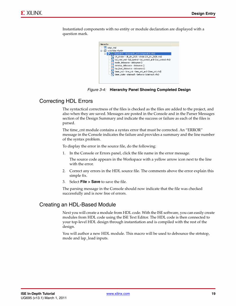
The Hierarchy pane in the Design panel displays all of the source files currently added to the project, with the associated entity or module names. Each source design unit is represented in the Hierarchy pane using the following syntax: instance name - entity name - architecture name - (file name).
ISE In-Depth Tutorial www.xilinx.com 19UG695 (v13.1) March 1, 2011
Design Entry
Instantiated components with no entity or module declaration are displayed with a question mark.
Correcting HDL ErrorsThe syntactical correctness of the files is checked as the files are added to the project, and also when they are saved. Messages are posted in the Console and in the Parser Messages section of the Design Summary and indicate the success or failure as each of the files is parsed.
The time_cnt module contains a syntax error that must be corrected. An “ERROR” message in the Console indicates the failure and provides a summary and the line number of the syntax problem.
To display the error in the source file, do the following:
1. In the Console or Errors panel, click the file name in the error message.
The source code appears in the Workspace with a yellow arrow icon next to the line with the error.
2. Correct any errors in the HDL source file. The comments above the error explain this simple fix.
3. Select File > Save to save the file.
The parsing message in the Console should now indicate that the file was checked successfully and is now free of errors.
Creating an HDL-Based ModuleNext you will create a module from HDL code. With the ISE software, you can easily create modules from HDL code using the ISE Text Editor. The HDL code is then connected to your top-level HDL design through instantiation and is compiled with the rest of the design.
You will author a new HDL module. This macro will be used to debounce the strtstop, mode and lap_load inputs.
X-Ref Target - Figure 3-4
Figure 3-4: Hierarchy Panel Showing Completed Design
20 www.xilinx.com ISE In-Depth TutorialUG695 (v13.1) March 1, 2011
Chapter 3: HDL-Based Design
Using the New Source Wizard and ISE Text Editor
In this section, you create a file using the New Source wizard, specifying the name and ports of the component. The resulting HDL file is then modified in the ISE Text Editor.
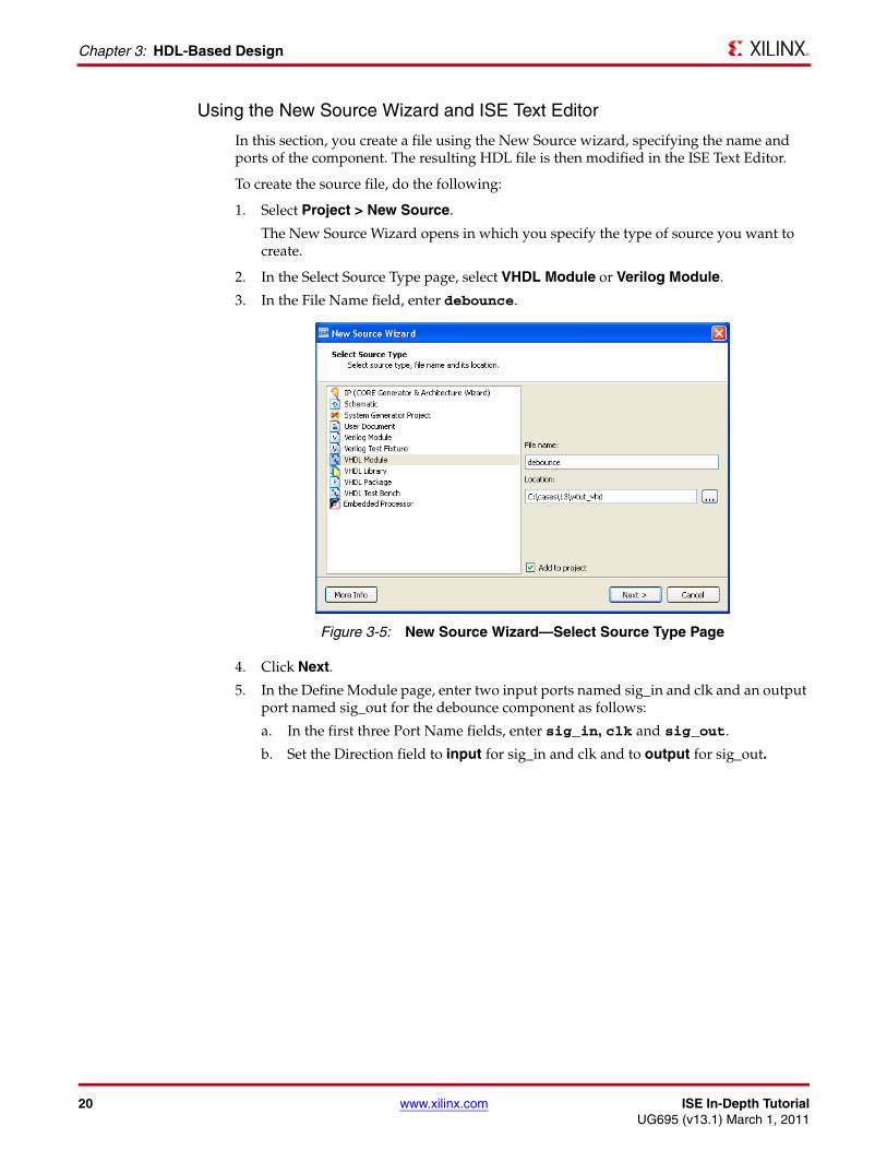
To create the source file, do the following:
1. Select Project > New Source.
The New Source Wizard opens in which you specify the type of source you want to create.
2. In the Select Source Type page, select VHDL Module or Verilog Module.
3. In the File Name field, enter debounce.
4. Click Next.
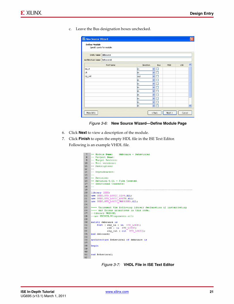
5. In the Define Module page, enter two input ports named sig_in and clk and an output port named sig_out for the debounce component as follows:
a. In the first three Port Name fields, enter sig_in, clk and sig_out.
b. Set the Direction field to input for sig_in and clk and to output for sig_out.
X-Ref Target - Figure 3-5
Figure 3-5: New Source Wizard—Select Source Type Page
ISE In-Depth Tutorial www.xilinx.com 21UG695 (v13.1) March 1, 2011
Design Entry
c. Leave the Bus designation boxes unchecked.
6. Click Next to view a description of the module.
7. Click Finish to open the empty HDL file in the ISE Text Editor.
Following is an example VHDL file.
X-Ref Target - Figure 3-6
Figure 3-6: New Source Wizard—Define Module Page
X-Ref Target - Figure 3-7
Figure 3-7: VHDL File in ISE Text Editor
22 www.xilinx.com ISE In-Depth TutorialUG695 (v13.1) March 1, 2011
Chapter 3: HDL-Based Design
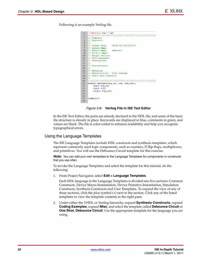
Following is an example Verilog file.
In the ISE Text Editor, the ports are already declared in the HDL file, and some of the basic file structure is already in place. Keywords are displayed in blue, comments in green, and values are black. The file is color-coded to enhance readability and help you recognize typographical errors.
Using the Language Templates
The ISE Language Templates include HDL constructs and synthesis templates, which represent commonly used logic components, such as counters, D flip-flops, multiplexers, and primitives. You will use the Debounce Circuit template for this exercise.
Note: You can add your own templates to the Language Templates for components or constructs that you use often.
To invoke the Language Templates and select the template for this tutorial, do the following:
1. From Project Navigator, select Edit > Language Templates.
Each HDL language in the Language Templates is divided into five sections: Common Constructs, Device Macro Instantiation, Device Primitive Instantiation, Simulation Constructs, Synthesis Constructs and User Templates. To expand the view of any of these sections, click the plus symbol (+) next to the section. Click any of the listed templates to view the template contents in the right pane.
2. Under either the VHDL or Verilog hierarchy, expand Synthesis Constructs, expand Coding Examples, expand Misc, and select the template called Debounce Circuit or One Shot, Debounce Circuit. Use the appropriate template for the language you are using.
X-Ref Target - Figure 3-8
Figure 3-8: Verilog File in ISE Text Editor
ISE In-Depth Tutorial www.xilinx.com 23UG695 (v13.1) March 1, 2011
Design Entry
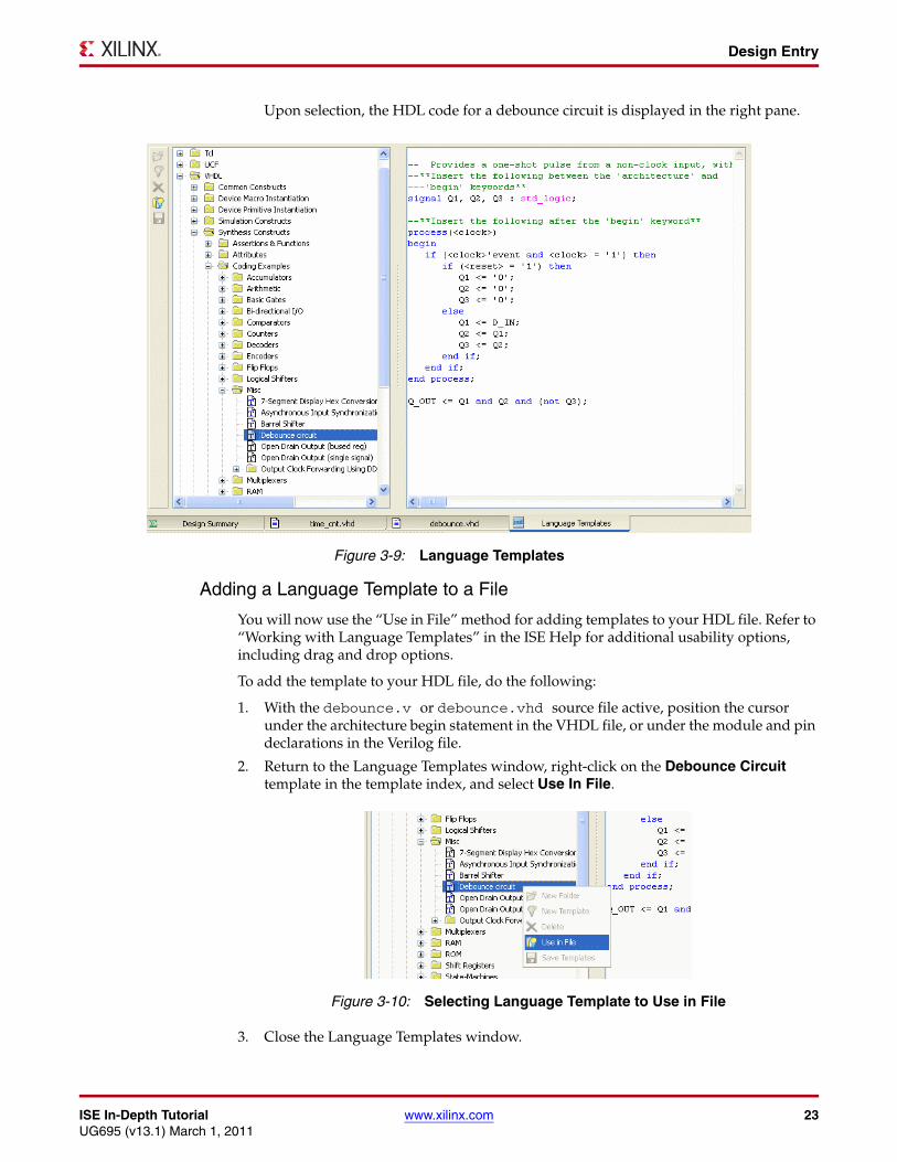
Upon selection, the HDL code for a debounce circuit is displayed in the right pane.
Adding a Language Template to a File
You will now use the “Use in File” method for adding templates to your HDL file. Refer to “Working with Language Templates” in the ISE Help for additional usability options, including drag and drop options.
To add the template to your HDL file, do the following:
1. With the debounce.v or debounce.vhd source file active, position the cursor under the architecture begin statement in the VHDL file, or under the module and pin declarations in the Verilog file.
2. Return to the Language Templates window, right-click on the Debounce Circuit template in the template index, and select Use In File.
3. Close the Language Templates window.
X-Ref Target - Figure 3-9
Figure 3-9: Language Templates
X-Ref Target - Figure 3-10
Figure 3-10: Selecting Language Template to Use in File

24 www.xilinx.com ISE In-Depth TutorialUG695 (v13.1) March 1, 2011
Chapter 3: HDL-Based Design
4. Open the debounce.v or debounce.vhd source file to verify that the Language Template was properly inserted.
5. Verilog only: Complete the Verilog module by doing the following:
a. Remove the reset logic (not used in this design) by deleting the three lines beginning with if and ending with else.
b. Change <reg_name> to q in all six locations.
c. Change <clock> to clk; <input> to sig_in; and <output> to sig_out.
Note: You can select Edit > Find & Replace to facilitate this. The Find fields appear at the bottom of the Text Editor.
6. VHDL only: Complete the VHDL module by doing the following:
a. Move the line beginning with the word signal so that it is between the architecture and begin keywords.
b. Remove the reset logic (not used in this design) by deleting the five lines beginning with if (<reset>... and ending with else, and delete one of the end if; lines.
c. Change <clock> to clk; D_IN to sig_in; and Q_OUT to sig_out.
Note: You can select Edit > Find & Replace to facilitate this. The Find fields appear at the bottom of the Text Editor.
7. Save the file by selecting File > Save.
8. Select one of the debounce instances in the Hierarchy pane.
9. In the Processes pane, double-click Check Syntax. Verify that the syntax check passes successfully. Correct any errors as necessary.
10. Close the ISE Text Editor.
Creating a CORE Generator Software ModuleThe CORE Generator software is a graphical interactive design tool that enables you to create high-level modules such as memory elements, math functions and communications, and I/O interface cores. You can customize and pre-optimize the modules to take advantage of the inherent architectural features of the Xilinx FPGA architectures, such as Fast Carry Logic, SRL16s, and distributed and block RAM.
In this section, you will create a CORE Generator software module called timer_preset. The module will be used to store a set of 64 values to load into the timer.
Creating the timer_preset CORE Generator Software Module
To create a CORE Generator software module, do the following:
1. In Project Navigator, select Project > New Source.
2. Select IP (CORE Generator & Architecture Wizard).
3. In the File Name field, enter timer_preset.
4. Click Next.
5. Expand the IP tree selector to locate Memories & Storage Elements > RAMs & ROMs.
ISE In-Depth Tutorial www.xilinx.com 25UG695 (v13.1) March 1, 2011
Design Entry
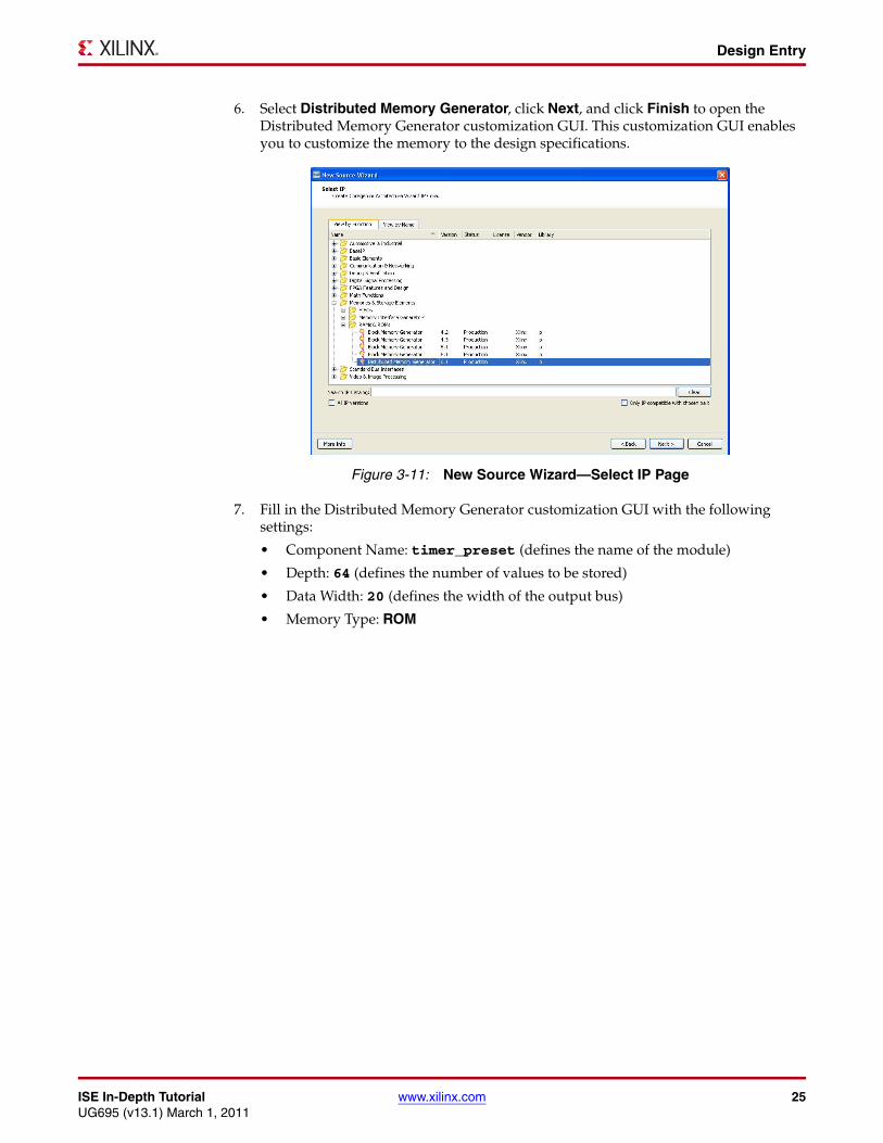
6. Select Distributed Memory Generator, click Next, and click Finish to open the Distributed Memory Generator customization GUI. This customization GUI enables you to customize the memory to the design specifications.
7. Fill in the Distributed Memory Generator customization GUI with the following settings:
• Component Name: timer_preset (defines the name of the module)
• Depth: 64 (defines the number of values to be stored)
• Data Width: 20 (defines the width of the output bus)
• Memory Type: ROM
X-Ref Target - Figure 3-11
Figure 3-11: New Source Wizard—Select IP Page
26 www.xilinx.com ISE In-Depth TutorialUG695 (v13.1) March 1, 2011
Chapter 3: HDL-Based Design
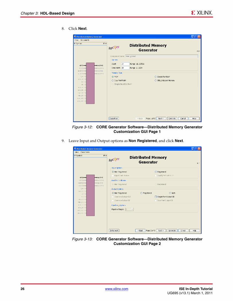
8. Click Next.
9. Leave Input and Output options as Non Registered, and click Next.
X-Ref Target - Figure 3-12
Figure 3-12: CORE Generator Software—Distributed Memory Generator Customization GUI Page 1
X-Ref Target - Figure 3-13
Figure 3-13: CORE Generator Software—Distributed Memory Generator Customization GUI Page 2
ISE In-Depth Tutorial www.xilinx.com 27UG695 (v13.1) March 1, 2011
Design Entry
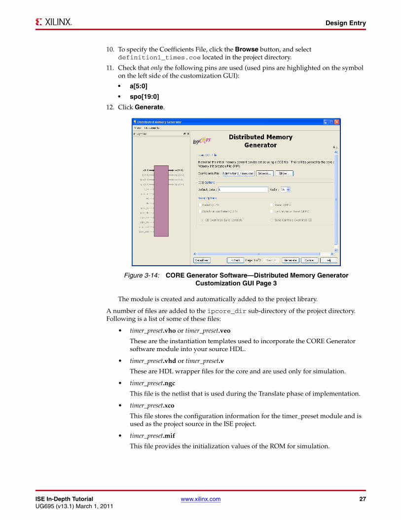
10. To specify the Coefficients File, click the Browse button, and select definition1_times.coe located in the project directory.
11. Check that only the following pins are used (used pins are highlighted on the symbol on the left side of the customization GUI):
• a[5:0]
• spo[19:0]
12. Click Generate.
The module is created and automatically added to the project library.
A number of files are added to the ipcore_dir sub-directory of the project directory. Following is a list of some of these files:
• timer_preset.vho or timer_preset.veo
These are the instantiation templates used to incorporate the CORE Generator software module into your source HDL.
• timer_preset.vhd or timer_preset.v
These are HDL wrapper files for the core and are used only for simulation.
• timer_preset.ngc
This file is the netlist that is used during the Translate phase of implementation.
• timer_preset.xco
This file stores the configuration information for the timer_preset module and is used as the project source in the ISE project.
• timer_preset.mif
This file provides the initialization values of the ROM for simulation.
X-Ref Target - Figure 3-14
Figure 3-14: CORE Generator Software—Distributed Memory Generator Customization GUI Page 3
28 www.xilinx.com ISE In-Depth TutorialUG695 (v13.1) March 1, 2011
Chapter 3: HDL-Based Design
Instantiating the CORE Generator Software Module in the HDL Code
Next, instantiate the CORE Generator software module in the HDL code using either a VHDL flow or a Verilog flow.
VHDL Flow
To instantiate the CORE Generator software module using a VHDL flow, do the following:
1. In Project Navigator, double-click stopwatch.vhd to open the file in ISE Text Editor.
2. Place the cursor after the following line:
-- Insert CORE Generator ROM component declaration here
3. Select Edit > Insert File, then select ipcore_dir/timer_preset.vho, and click Open.
The VHDL template file for the CORE Generator software instantiation is inserted.
4. Highlight the inserted code from:
-- Begin Cut here for INSTANTIATION Template ----
to
--INST_TAG_END ------ END INSTANTIATION Template -----
5. Select Edit > Cut.
6. Place the cursor after the following line:
--Insert CORE Generator ROM Instantiation here
7. Select Edit > Paste to place the core instantiation.
8. Change the instance name from your_instance_name to t_preset.
9. Edit this instantiated code to connect the signals in the stopwatch design to the ports of the CORE Generator software module as shown below.
10. The inserted code of timer_preset.vho contains several lines of commented text for instruction and legal documentation. Delete these commented lines if desired.
11. Save the design using File > Save, and close the ISE Text Editor.
X-Ref Target - Figure 3-15
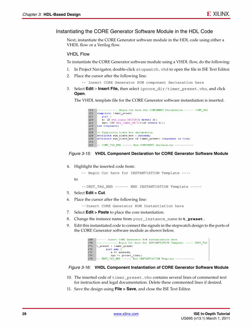
Figure 3-15: VHDL Component Declaration for CORE Generator Software Module
X-Ref Target - Figure 3-16
Figure 3-16: VHDL Component Instantiation of CORE Generator Software Module
ISE In-Depth Tutorial www.xilinx.com 29UG695 (v13.1) March 1, 2011
Design Entry
Verilog Flow
To instantiate the CORE Generator software module using a Verilog flow, do the following:
1. In Project Navigator, double-click stopwatch.v to open the file in the ISE Text Editor.
2. Place the cursor after the following line:
//Place the Coregen module instantiation for timer_preset here
3. Select Edit > Insert File, and select ipcore_dir/timer_preset.veo.
4. The inserted code of timer_preset.veo contains several lines of commented text for instruction and legal documentation. Delete these commented lines if desired.
5. Change the instance name from YourInstanceName to t_preset.
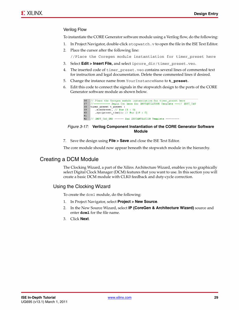
6. Edit this code to connect the signals in the stopwatch design to the ports of the CORE Generator software module as shown below.
7. Save the design using File > Save and close the ISE Text Editor.
The core module should now appear beneath the stopwatch module in the hierarchy.
Creating a DCM ModuleThe Clocking Wizard, a part of the Xilinx Architecture Wizard, enables you to graphically select Digital Clock Manager (DCM) features that you want to use. In this section you will create a basic DCM module with CLK0 feedback and duty-cycle correction.
Using the Clocking Wizard
To create the dcm1 module, do the following:
1. In Project Navigator, select Project > New Source.
2. In the New Source Wizard, select IP (CoreGen & Architecture Wizard) source and enter dcm1 for the file name.
3. Click Next.
X-Ref Target - Figure 3-17
Figure 3-17: Verilog Component Instantiation of the CORE Generator Software Module
30 www.xilinx.com ISE In-Depth TutorialUG695 (v13.1) March 1, 2011
Chapter 3: HDL-Based Design
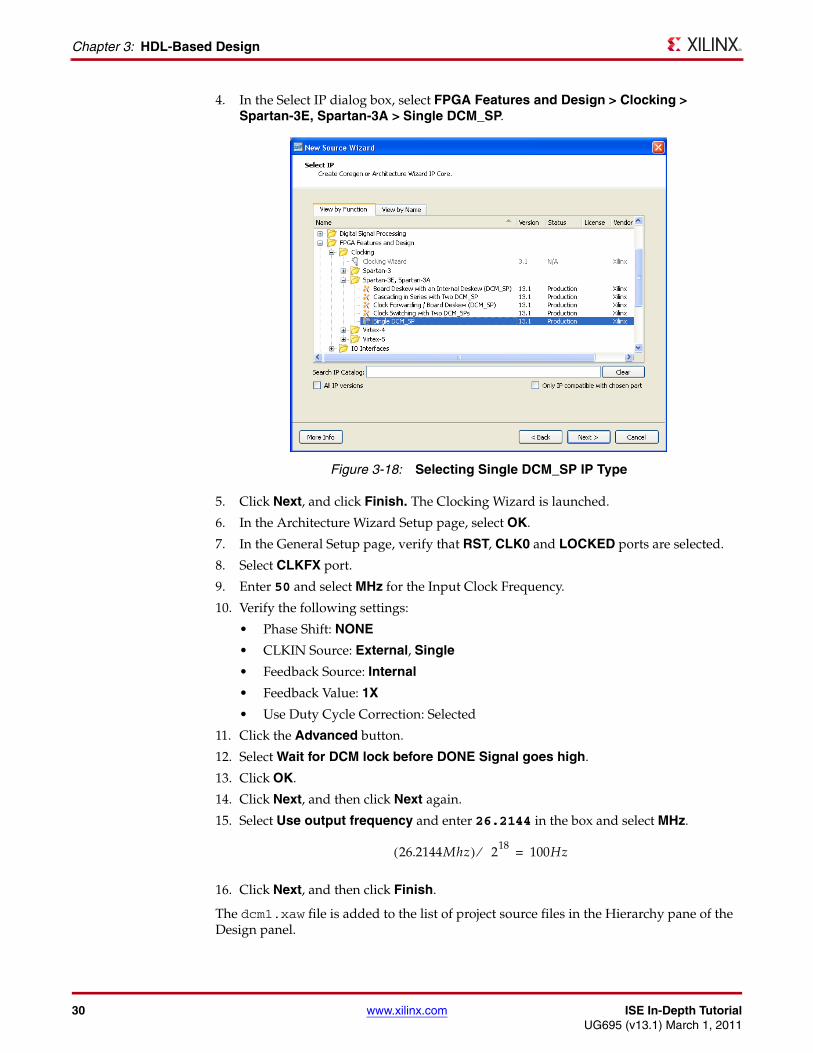
4. In the Select IP dialog box, select FPGA Features and Design > Clocking > Spartan-3E, Spartan-3A > Single DCM_SP.
5. Click Next, and click Finish. The Clocking Wizard is launched.
6. In the Architecture Wizard Setup page, select OK.
7. In the General Setup page, verify that RST, CLK0 and LOCKED ports are selected.
8. Select CLKFX port.
9. Enter 50 and select MHz for the Input Clock Frequency.
10. Verify the following settings:
• Phase Shift: NONE
• CLKIN Source: External, Single
• Feedback Source: Internal
• Feedback Value: 1X
• Use Duty Cycle Correction: Selected
11. Click the Advanced button.
12. Select Wait for DCM lock before DONE Signal goes high.
13. Click OK.
14. Click Next, and then click Next again.
15. Select Use output frequency and enter 26.2144 in the box and select MHz.
16. Click Next, and then click Finish.
The dcm1.xaw file is added to the list of project source files in the Hierarchy pane of the Design panel.
X-Ref Target - Figure 3-18
Figure 3-18: Selecting Single DCM_SP IP Type
26.2144Mhz( ) 218⁄ 100Hz=
ISE In-Depth Tutorial www.xilinx.com 31UG695 (v13.1) March 1, 2011
Design Entry
Instantiating the dcm1 Macro—VHDL Design
Next, you will instantiate the dcm1 macro for your VHDL or Verilog design. To instantiate the dcm1 macro for the VHDL design, do the following:
1. In the Hierarchy pane of the Project Navigator Design panel, select dcm1.xaw.
2. In the Processes pane, right-click View HDL Instantiation Template, and select Process Properties.
3. Choose VHDL for the HDL Instantiation Template Target Language value, and click OK.
4. In the Processes pane, double-click View HDL Instantiation Template.
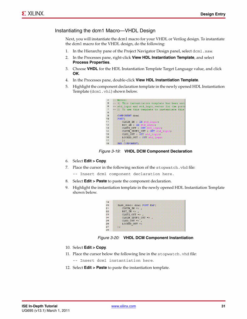
5. Highlight the component declaration template in the newly opened HDL Instantiation Template (dcm1.vhi) shown below.
6. Select Edit > Copy.
7. Place the cursor in the following section of the stopwatch.vhd file:
-- Insert dcm1 component declaration here.
8. Select Edit > Paste to paste the component declaration.
9. Highlight the instantiation template in the newly opened HDL Instantiation Template shown below.
10. Select Edit > Copy.
11. Place the cursor below the following line in the stopwatch.vhd file:
-- Insert dcm1 instantiation here.
12. Select Edit > Paste to paste the instantiation template.
X-Ref Target - Figure 3-19
Figure 3-19: VHDL DCM Component Declaration
X-Ref Target - Figure 3-20
Figure 3-20: VHDL DCM Component Instantiation
32 www.xilinx.com ISE In-Depth TutorialUG695 (v13.1) March 1, 2011
Chapter 3: HDL-Based Design
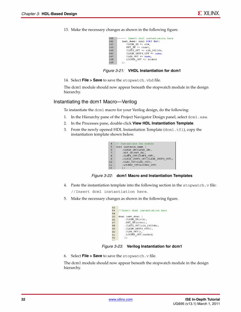
13. Make the necessary changes as shown in the following figure.
14. Select File > Save to save the stopwatch.vhd file.
The dcm1 module should now appear beneath the stopwatch module in the design hierarchy.
Instantiating the dcm1 Macro—Verilog
To instantiate the dcm1 macro for your Verilog design, do the following:
1. In the Hierarchy pane of the Project Navigator Design panel, select dcm1.xaw.
2. In the Processes pane, double-click View HDL Instantiation Template.
3. From the newly opened HDL Instantiation Template (dcm1.tfi), copy the instantiation template shown below.
4. Paste the instantiation template into the following section in the stopwatch.v file:
//Insert dcm1 instantiation here.
5. Make the necessary changes as shown in the following figure.
6. Select File > Save to save the stopwatch.v file.
The dcm1 module should now appear beneath the stopwatch module in the design hierarchy.
X-Ref Target - Figure 3-21
Figure 3-21: VHDL Instantiation for dcm1
X-Ref Target - Figure 3-22
Figure 3-22: dcm1 Macro and Instantiation Templates
X-Ref Target - Figure 3-23
Figure 3-23: Verilog Instantiation for dcm1
ISE In-Depth Tutorial www.xilinx.com 33UG695 (v13.1) March 1, 2011
Synthesizing the Design
Synthesizing the DesignSo far you have been using Xilinx Synthesis Technology (XST) for syntax checking. Next, you will synthesize the design using either XST, Synplify/Synplify Pro, or Precision software. The synthesis tool uses the design’s HDL code and generates a supported netlist type (EDIF or NGC) for the Xilinx implementation tools. The synthesis tool performs the following general steps (although all synthesis tools further break down these general steps) to create the netlist:
• Analyze/Check Syntax
Checks the syntax of the source code.
• Compile
Translates and optimizes the HDL code into a set of components that the synthesis tool can recognize.
• Map
Translates the components from the compile stage into the target technology’s primitive components.
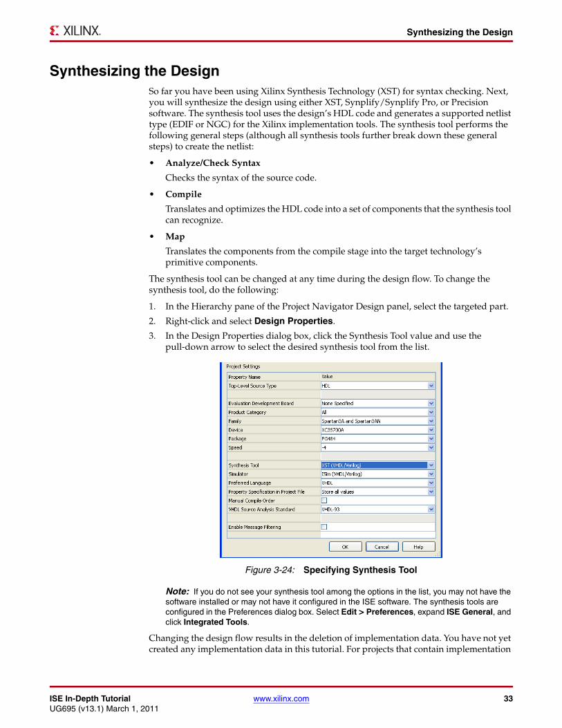
The synthesis tool can be changed at any time during the design flow. To change the synthesis tool, do the following:
1. In the Hierarchy pane of the Project Navigator Design panel, select the targeted part.
2. Right-click and select Design Properties.
3. In the Design Properties dialog box, click the Synthesis Tool value and use the pull-down arrow to select the desired synthesis tool from the list.
Note: If you do not see your synthesis tool among the options in the list, you may not have the software installed or may not have it configured in the ISE software. The synthesis tools are configured in the Preferences dialog box. Select Edit > Preferences, expand ISE General, and click Integrated Tools.
Changing the design flow results in the deletion of implementation data. You have not yet created any implementation data in this tutorial. For projects that contain implementation
X-Ref Target - Figure 3-24
Figure 3-24: Specifying Synthesis Tool

34 www.xilinx.com ISE In-Depth TutorialUG695 (v13.1) March 1, 2011
Chapter 3: HDL-Based Design
data, Xilinx recommends that you make a copy of the project using File > Copy Project if you would like to make a backup of the project before continuing.
Synthesizing the Design Using XSTNow that you have created and analyzed the design, the next step is to synthesize the design. During synthesis, the HDL files are translated into gates and optimized for the target architecture.
Processes available for synthesis using XST are as follows:
• View RTL Schematic
Generates a schematic view of your RTL netlist.
• View Technology Schematic
Generates a schematic view of your technology netlist.
• Check Syntax
Verifies that the HDL code is entered properly.
• Generate Post-Synthesis Simulation Model
Creates HDL simulation models based on the synthesis netlist.
Entering Synthesis Options
Synthesis options enable you to modify the behavior of the synthesis tool to make optimizations according to the needs of the design. One commonly used option is to control synthesis to make optimizations based on area or speed. Other options include controlling the maximum fanout of a flip-flop output or setting the desired frequency of the design.
To enter synthesis options, do the following:
1. In the Hierarchy pane of the Project Navigator Design panel, select stopwatch.vhd (or stopwatch.v).
2. In the Processes pane, right-click the Synthesize process, and select Process Properties.
3. Under the Synthesis Options tab, set the Netlist Hierarchy property to a value of Rebuilt.
Note: To use this property, you must set the Property display level to Advanced.
4. Click OK.
Synthesizing the Design
Now you are ready to synthesize your design. To take the HDL code and generate a compatible netlist, do the following:
1. In the Hierarchy pane, select stopwatch.vhd (or stopwatch.v).
2. In the Processes pane, double-click the Synthesize process.
ISE In-Depth Tutorial www.xilinx.com 35UG695 (v13.1) March 1, 2011
Synthesizing the Design
Using the RTL/Technology Viewer
XST can generate a schematic representation of the HDL code that you have entered. A schematic view of the code helps you analyze your design by displaying a graphical connection between the various components that XST has inferred. Following are the two forms of schematic representation:
• RTL View
Pre-optimization of the HDL code.
• Technology View
Post-synthesis view of the HDL design mapped to the target technology.
To view a schematic representation of your HDL code, do the following:
1. In the Processes pane, expand Synthesize, and double-click View RTL Schematic or View Technology Schematic.
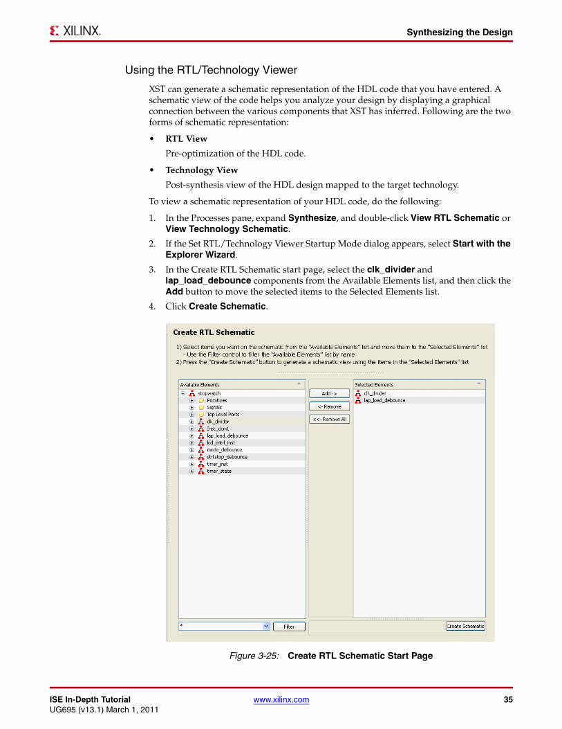
2. If the Set RTL/Technology Viewer Startup Mode dialog appears, select Start with the Explorer Wizard.
3. In the Create RTL Schematic start page, select the clk_divider and lap_load_debounce components from the Available Elements list, and then click the Add button to move the selected items to the Selected Elements list.
4. Click Create Schematic.X-Ref Target - Figure 3-25
Figure 3-25: Create RTL Schematic Start Page
36 www.xilinx.com ISE In-Depth TutorialUG695 (v13.1) March 1, 2011
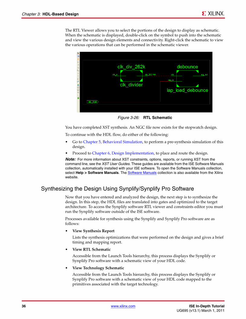
Chapter 3: HDL-Based Design
The RTL Viewer allows you to select the portions of the design to display as schematic. When the schematic is displayed, double-click on the symbol to push into the schematic and view the various design elements and connectivity. Right-click the schematic to view the various operations that can be performed in the schematic viewer.
You have completed XST synthesis. An NGC file now exists for the stopwatch design.
To continue with the HDL flow, do either of the following:
• Go to Chapter 5, Behavioral Simulation, to perform a pre-synthesis simulation of this design.
• Proceed to Chapter 6, Design Implementation, to place and route the design.
Note: For more information about XST constraints, options, reports, or running XST from the command line, see the XST User Guides. These guides are available from the ISE Software Manuals collection, automatically installed with your ISE software. To open the Software Manuals collection, select Help > Software Manuals. The Software Manuals collection is also available from the Xilinx website.
Synthesizing the Design Using Synplify/Synplify Pro SoftwareNow that you have entered and analyzed the design, the next step is to synthesize the design. In this step, the HDL files are translated into gates and optimized to the target architecture. To access the Synplify software RTL viewer and constraints editor you must run the Synplify software outside of the ISE software.
Processes available for synthesis using the Synplify and Synplify Pro software are as follows:
• View Synthesis Report
Lists the synthesis optimizations that were performed on the design and gives a brief timing and mapping report.
• View RTL Schematic
Accessible from the Launch Tools hierarchy, this process displays the Synplify or Synplify Pro software with a schematic view of your HDL code.
• View Technology Schematic
Accessible from the Launch Tools hierarchy, this process displays the Synplify or Synplify Pro software with a schematic view of your HDL code mapped to the primitives associated with the target technology.
X-Ref Target - Figure 3-26
Figure 3-26: RTL Schematic

ISE In-Depth Tutorial www.xilinx.com 37UG695 (v13.1) March 1, 2011
Synthesizing the Design
Entering Synthesis Options and Synthesizing the Design
To synthesize the design, set the global synthesis options as follows:
1. In the Hierarchy pane of the Project Navigator Design panel, select stopwatch.vhd (or stopwatch.v).
2. In the Processes pane, right-click Synthesize, and select Process Properties.
3. In the Synthesis Options dialog box, select the Write Vendor Constraint File box.
4. Click OK to accept these values.
5. Double-click the Synthesize process to run synthesis.
Note: This step can also be done by selecting stopwatch.vhd (or stopwatch.v), clicking Synthesize in the Processes pane, and selecting Process > Run.
Examining Synthesis Results
To view overall synthesis results, double-click View Synthesis Report under the Synthesize process. The report consists of the following sections:
• Compiler Report
• Mapper Report
• Timing Report
• Resource Utilization
Compiler Report
The compiler report lists each HDL file that was compiled, names which file is the top level, and displays the syntax checking result for each file that was compiled. The report also lists FSM extractions, inferred memory, warnings on latches, unused ports, and removal of redundant logic.
Note: Black boxes (modules not read into a design environment) are always noted as unbound in the Synplify reports. As long as the underlying netlist (.ngo, .ngc or .edn) for a black box exists in the project directory, the implementation tools merge the netlist into the design during the Translate phase.
Mapper Report
The mapper report lists the constraint files used, the target technology, and attributes set in the design. The report lists the mapping results of flattened instances, extracted counters, optimized flip-flops, clock and buffered nets that were created, and how FSMs were coded.
Timing Report
The timing report section provides detailed information on the constraints that you entered and on delays on parts of the design that had no constraints. The delay values are based on wireload models and are considered preliminary. Consult the post-Place and
38 www.xilinx.com ISE In-Depth TutorialUG695 (v13.1) March 1, 2011
Chapter 3: HDL-Based Design
Route timing reports discussed in Chapter 6, Design Implementation, for the most accurate delay information.
Resource Utilization
This section of the report lists all of the resources that the Synplify software uses for the given target technology.
You have now completed Synplify synthesis. At this point, a netlist EDN file exists for the stopwatch design.
To continue with the HDL flow, do either of the following:
• Go to Chapter 5, Behavioral Simulation, to perform a pre-synthesis simulation of this design.
• Proceed to Chapter 6, Design Implementation, to place and route the design.
Synthesizing the Design Using Precision SynthesisNow that you have entered and analyzed the design, the next step is to synthesize the design. In this step, the HDL files are translated into gates and optimized to the target architecture.
Processes available for synthesis using the Precision software are as follows:
• Check Syntax
Checks the syntax of the HDL code.
• View Log File
Lists the synthesis optimizations that were performed on the design and gives a brief timing and mapping report.
• View RTL Schematic
Accessible from the Launch Tools hierarchy, this process displays the Precision software with a schematic view of your HDL code.
• View Technology Schematic
Accessible from the Launch Tools hierarchy, this process displays the Precision software with a schematic view of your HDL code mapped to the primitives associated with the target technology.
• View Critical Path Schematic
Accessible from the Launch Tools hierarchy, this process displays the Precision software with a schematic view of the critical path of your HDL code mapped to the primitives associated with the target technology.
X-Ref Target - Figure 3-27
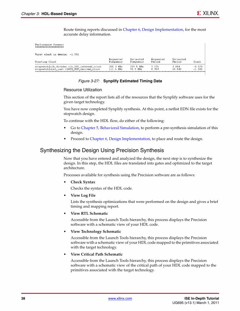
Figure 3-27: Synplify Estimated Timing Data
ISE In-Depth Tutorial www.xilinx.com 39UG695 (v13.1) March 1, 2011
Synthesizing the Design
Entering Synthesis Options and Synthesizing the Design
Synthesis options enable you to modify the behavior of the synthesis tool to optimize according to the needs of the design. For the tutorial, the default property settings will be used.
To synthesize the design, do the following:
1. In the Hierarchy pane of the Project Navigator Design panel, select stopwatch.vhd (or stopwatch.v).
2. In the Processes pane, double-click the Synthesize process.
Using the RTL/Technology Viewer
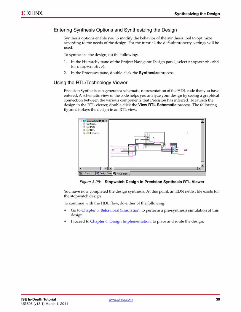
Precision Synthesis can generate a schematic representation of the HDL code that you have entered. A schematic view of the code helps you analyze your design by seeing a graphical connection between the various components that Precision has inferred. To launch the design in the RTL viewer, double-click the View RTL Schematic process. The following figure displays the design in an RTL view.
You have now completed the design synthesis. At this point, an EDN netlist file exists for the stopwatch design.
To continue with the HDL flow, do either of the following:
• Go to Chapter 5, Behavioral Simulation, to perform a pre-synthesis simulation of this design.
• Proceed to Chapter 6, Design Implementation, to place and route the design.
X-Ref Target - Figure 3-28
Figure 3-28: Stopwatch Design in Precision Synthesis RTL Viewer

40 www.xilinx.com ISE In-Depth TutorialUG695 (v13.1) March 1, 2011
Chapter 3: HDL-Based Design
ISE In-Depth Tutorial www.xilinx.com 41UG695 (v13.1) March 1, 2011
Chapter 4
Schematic-Based Design
Overview of Schematic-Based DesignThis chapter guides you through a typical FPGA schematic-based design procedure using the design of a runner’s stopwatch. The design example used in this tutorial demonstrates many device features, software features, and design flow practices that you can apply to your own designs. The stopwatch design targets a Spartan™-3A device; however, all of the principles and flows taught are applicable to any Xilinx® device family, unless otherwise noted.
This chapter is the first in the Schematic Design Flow. In the first part of the tutorial, you will use the ISE® design entry tools to complete the design. The design is composed of schematic elements, CORE Generator™ software components, and HDL macros. After the design is successfully entered in the Schematic Editor, you will perform behavioral simulation (Chapter 5, Behavioral Simulation), run implementation with the Xilinx implementation tools (Chapter 6, Design Implementation), perform timing simulation (Chapter 7, Timing Simulation), and configure and download to the Spartan-3A (XC3S700A) demo board (see Chapter 8, Configuration Using iMPACT).
Getting StartedThe following sections describe the basic requirements for running the tutorial.
Required SoftwareTo perform this tutorial, you must have Xilinx ISE Design Suite installed. For this design, you must install the Spartan-3A device libraries and device files.
42 www.xilinx.com ISE In-Depth TutorialUG695 (v13.1) March 1, 2011
Chapter 4: Schematic-Based Design
This tutorial assumes that the software is installed in the default location, at c:\xilinx\release_number\ISE_DS\ISE. If you installed the software in a different location, substitute your installation path in the procedures that follow.
Note: For detailed software installation instructions, refer to the ISE Design Suite: Installation and Licensing Guide (UG798) available from the Xilinx website.
Installing the Tutorial Project FilesThe tutorial project files are provided with the ISE Design Suite Tutorials available from the Xilinx website. Download the schematic design files (wtut_sc.zip). The download contains the following directories:
• wtut_sc
Contains source files for the schematic tutorial. The schematic tutorial project will be created in this directory.
• wtut_sc\wtut_sc_completed
Contains the completed design files for the schematic tutorial design, including schematic, HDL, and state machine files.
Note: Do not overwrite files under this directory.
The schematic tutorial files are copied into the directories when you unzip the files. This tutorial assumes that the files are unzipped under c:\xilinx_tutorial, but you can unzip the source files into any directory with read/write permissions. If you unzip the files into a different location, substitute your project path in the procedures that follow.
Starting the ISE SoftwareTo launch the ISE software, double-click the ISE Project Navigator icon on your desktop, or select Start > All Programs > Xilinx ISE Design Suite > ISE Design Tools > Project Navigator.
Creating a New ProjectTo create a new project using the New Project Wizard, do the following:
1. From Project Navigator, select File > New Project.
2. In the Location field, browse to c:\xilinx_tutorial or to the directory in which you installed the project.
3. In the Name field, enter wtut_sc.
4. Select Schematic as the Top-Level Source Type, and then click Next.
5. Select the following values in the New Project Wizard—Device Properties page:
• Product Category: All
• Family: Spartan3A and Spartan3AN
• Device: XC3S700A
X-Ref Target - Figure 4-1
Figure 4-1: Project Navigator Desktop Icon
ISE In-Depth Tutorial www.xilinx.com 43UG695 (v13.1) March 1, 2011
Design Description
• Package: FG484
• Speed: -4
• Synthesis Tool: XST (VHDL/Verilog)
• Simulator: ISim (VHDL/Verilog)
• Preferred Language: VHDL or Verilog depending on preference. This will determine the default language for all processes that generate HDL files.
Other properties can be left at their default values.
6. Click Next, then Finish to complete the project creation.
Stopping the TutorialIf you need to stop the tutorial at any time, save your work by selecting File > Save All.
Design DescriptionThe design used in this tutorial is a hierarchical, schematic-based design, which means that the top-level design file is a schematic sheet that refers to several other lower-level macros. The lower-level macros are a variety of different types of modules, including schematic-based modules, a CORE Generator software module, an Architecture Wizard module, and HDL modules.
The runner’s stopwatch design begins as an unfinished design. Throughout the tutorial, you will complete the design by creating some of the modules and by completing others from existing files. Through the course of this chapter, you will create these modules,
44 www.xilinx.com ISE In-Depth TutorialUG695 (v13.1) March 1, 2011
Chapter 4: Schematic-Based Design
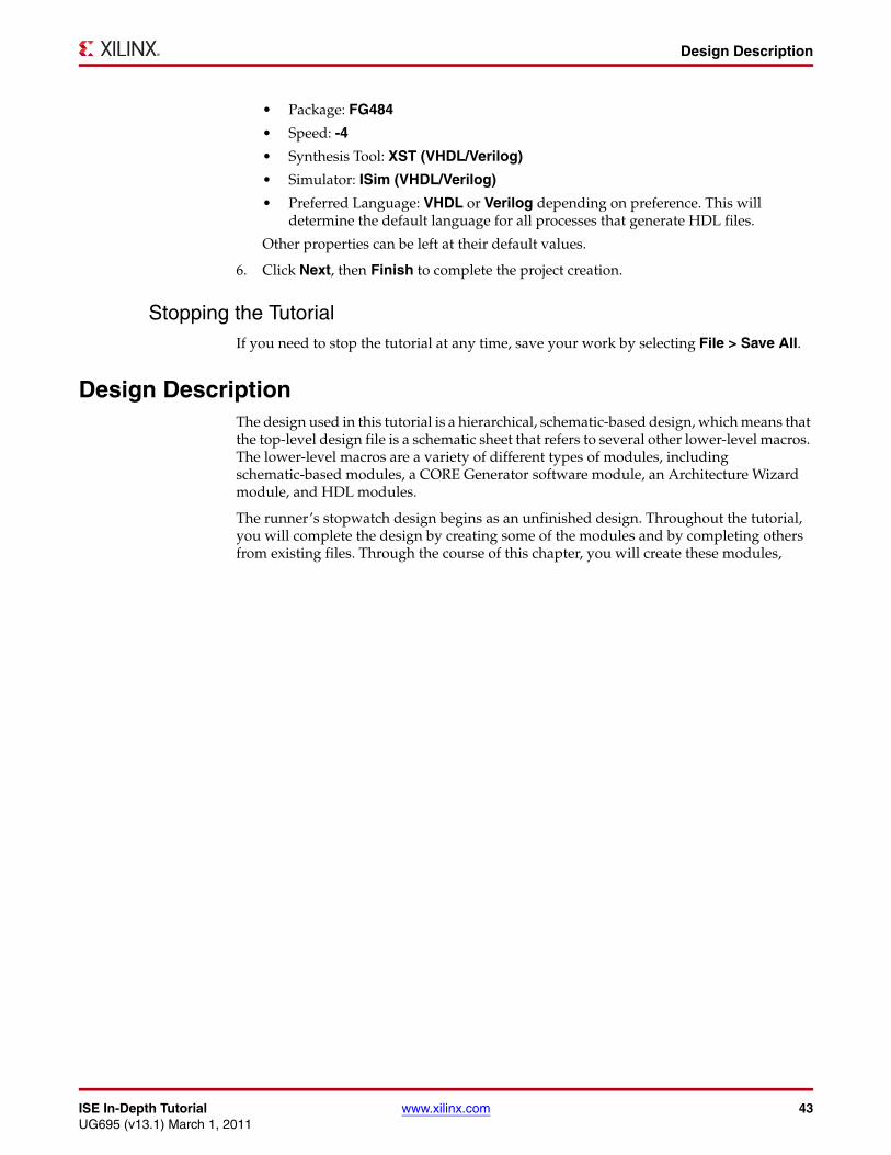
instantiate them, and then connect them. The following figure shows a schematic of the completed stopwatch design.
After the design is complete, you will simulate the design to verify its functionality. For more information about simulating your design, see Chapter 5, Behavioral Simulation.
There are five external inputs and four external outputs in the completed design. The following sections summarize the inputs and outputs, and their respective functions.
InputsThe following are input signals for the tutorial stopwatch design:
• strtstop
Starts and stops the stopwatch. This is an active low signal which acts like the start/stop button on a runner’s stopwatch.
• reset
Puts the stopwatch in clocking mode and resets the time to 0:00:00.
• clk
Externally generated system clock.
• mode
Toggles between clocking and timer modes. This input is only functional while the clock or timer is not counting.
X-Ref Target - Figure 4-2
Figure 4-2: Completed Stopwatch Schematic
ISE In-Depth Tutorial www.xilinx.com 45UG695 (v13.1) March 1, 2011
Design Description
• lap_load
This is a dual function signal. In clocking mode it displays the current clock value in the ‘Lap’ display area. In timer mode it will load the pre-assigned values from the ROM to the timer display when the timer is not counting.
OutputsThe following are outputs signals for the design:
• lcd_e, lcd_rs, lcd_rw
These outputs are the control signals for the LCD display of the Spartan-3A demo board used to display the stopwatch times.
• sf_d[7:0]
Provides the data values for the LCD display.
Functional BlocksThe completed design consists of the following functional blocks. Most of these blocks do not appear on the schematic sheet in the project until after you create and add them to the schematic during this tutorial.
The completed design consists of the following functional blocks:
• clk_div_262k
Macro which divides a clock frequency by 262,144. Converts 26.2144 MHz clock into 100 Hz 50% duty cycle clock.
• dcm1
Clocking Wizard macro with internal feedback, frequency controlled output, and duty-cycle correction. The CLKFX_OUT output converts the 50 MHz clock of the Spartan-3A demo board to 26.2144 MHz.
• debounce
Module implementing a simplistic debounce circuit for the strtstop, mode, and lap_load input signals.
• lcd_control
Module controlling the initialization of and output to the LCD display.
• statmach
State machine module which controls the state of the stopwatch.
• timer_preset
CORE Generator software 64X20 ROM. This macro contains 64 preset times from 0:00:00 to 9:59:99 which can be loaded into the timer.
• time_cnt
Up/down counter module which counts between 0:00:00 to 9:59:99 decimal. This macro has five 4-bit outputs, which represent the digits of the stopwatch time.
46 www.xilinx.com ISE In-Depth TutorialUG695 (v13.1) March 1, 2011
Chapter 4: Schematic-Based Design
Design EntryIn this hierarchical design, you will create various types of macros, including schematic-based macros, HDL-based macros, and CORE Generator software macros. You will learn the process for creating each of these types of macros, and you will connect the macros together to create the completed stopwatch design. All procedures used in the tutorial can be used later for your own designs.
Adding Source FilesSource files must be added to the project before the design can be edited, synthesized and implemented. You will add six source files to the project as follows:
1. Select Project > Add Source.
2. Select the following files from the project directory and click Open.
• cd4rled.sch
• ch4rled.sch
• clk_div_262k.vhd
• lcd_control.vhd
• stopwatch.sch
• statmach.vhd
3. In the Adding Source Files dialog box, verify that the files are associated with All, that the associated library is work, and click OK.
The Hierarchy pane in the Design panel displays all of the source files currently added to the project, with the associated entity or module names.
Opening the Schematic File in the Xilinx Schematic EditorThe stopwatch schematic available in the wtut_sc project is incomplete. In this tutorial, you will update the schematic in the Schematic Editor. After you create the project in the ISE software and add the source files, you can open the stopwatch.sch file for editing. To open the schematic file, double-click stopwatch.sch in the Hierarchy pane of the Design panel.
ISE In-Depth Tutorial www.xilinx.com 47UG695 (v13.1) March 1, 2011
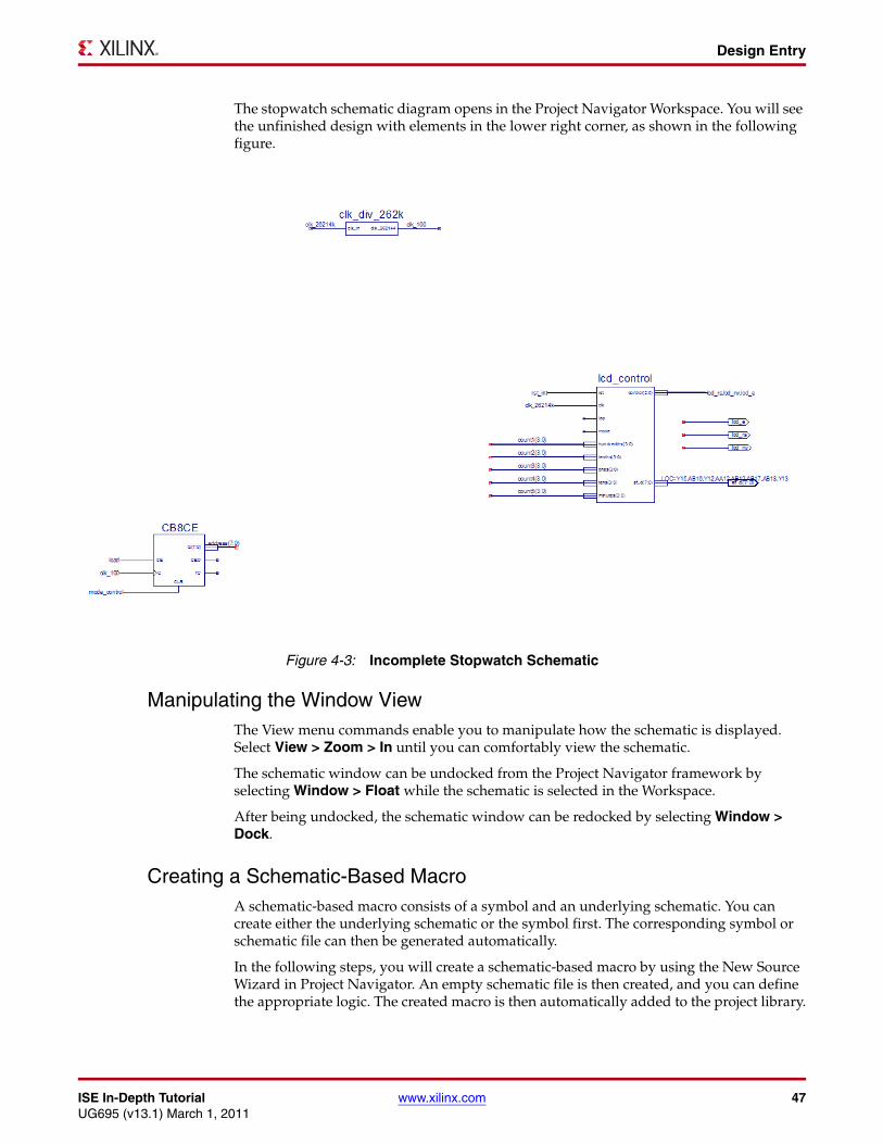
Design Entry
The stopwatch schematic diagram opens in the Project Navigator Workspace. You will see the unfinished design with elements in the lower right corner, as shown in the following figure.
Manipulating the Window ViewThe View menu commands enable you to manipulate how the schematic is displayed. Select View > Zoom > In until you can comfortably view the schematic.
The schematic window can be undocked from the Project Navigator framework by selecting Window > Float while the schematic is selected in the Workspace.
After being undocked, the schematic window can be redocked by selecting Window > Dock.
Creating a Schematic-Based MacroA schematic-based macro consists of a symbol and an underlying schematic. You can create either the underlying schematic or the symbol first. The corresponding symbol or schematic file can then be generated automatically.
In the following steps, you will create a schematic-based macro by using the New Source Wizard in Project Navigator. An empty schematic file is then created, and you can define the appropriate logic. The created macro is then automatically added to the project library.
X-Ref Target - Figure 4-3
Figure 4-3: Incomplete Stopwatch Schematic
48 www.xilinx.com ISE In-Depth TutorialUG695 (v13.1) March 1, 2011
Chapter 4: Schematic-Based Design
The macro you will create is called time_cnt. This macro is a binary counter with five, 4-bit outputs, representing the digits of the stopwatch.
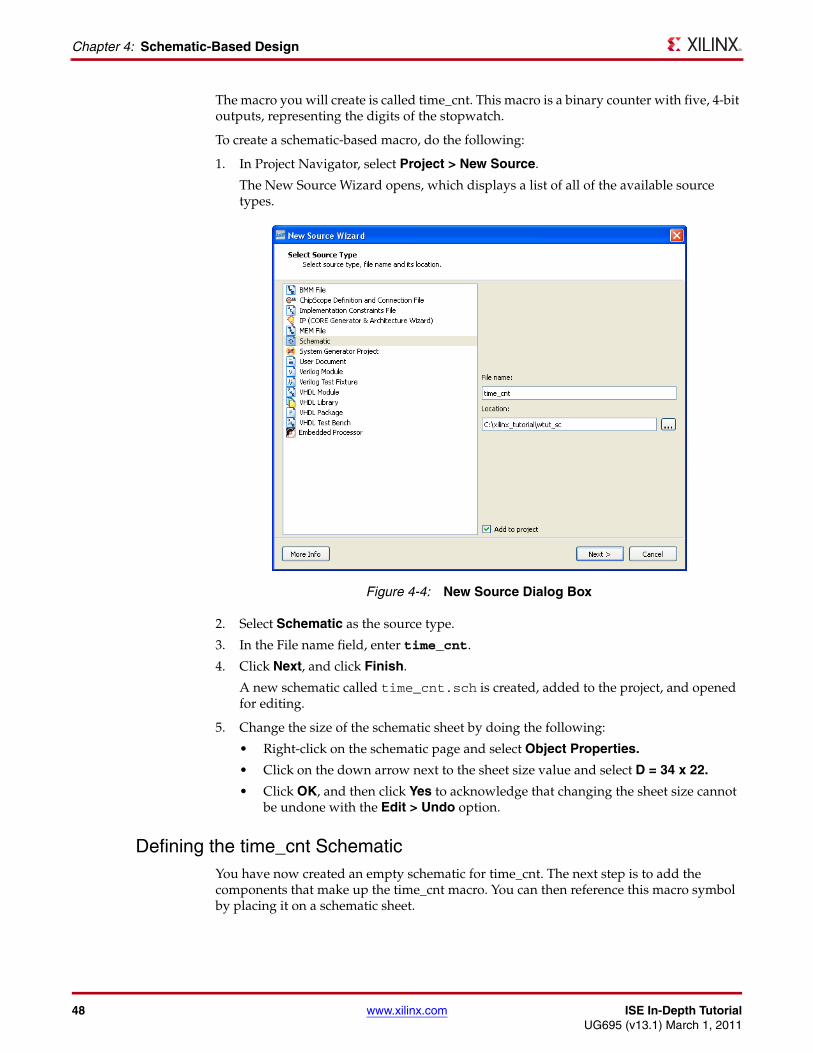
To create a schematic-based macro, do the following:
1. In Project Navigator, select Project > New Source.
The New Source Wizard opens, which displays a list of all of the available source types.
2. Select Schematic as the source type.
3. In the File name field, enter time_cnt.
4. Click Next, and click Finish.
A new schematic called time_cnt.sch is created, added to the project, and opened for editing.
5. Change the size of the schematic sheet by doing the following:
• Right-click on the schematic page and select Object Properties.
• Click on the down arrow next to the sheet size value and select D = 34 x 22.
• Click OK, and then click Yes to acknowledge that changing the sheet size cannot be undone with the Edit > Undo option.
Defining the time_cnt SchematicYou have now created an empty schematic for time_cnt. The next step is to add the components that make up the time_cnt macro. You can then reference this macro symbol by placing it on a schematic sheet.
X-Ref Target - Figure 4-4
Figure 4-4: New Source Dialog Box
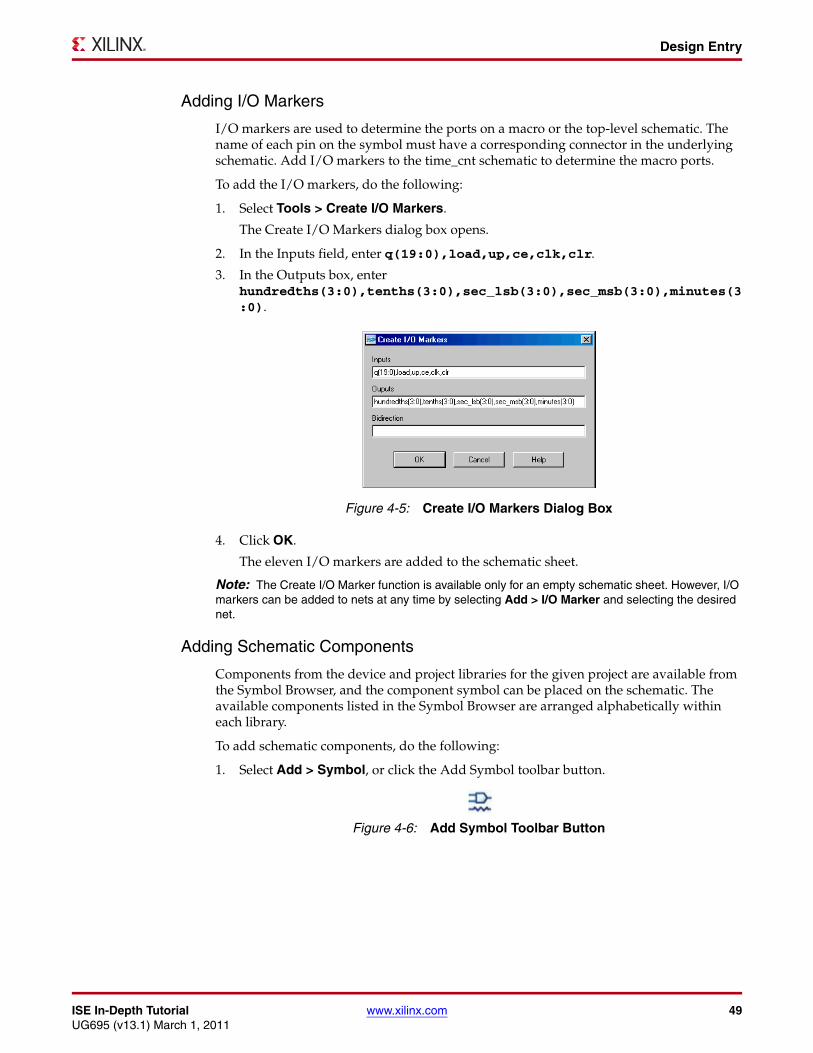
ISE In-Depth Tutorial www.xilinx.com 49UG695 (v13.1) March 1, 2011
Design Entry
Adding I/O Markers
I/O markers are used to determine the ports on a macro or the top-level schematic. The name of each pin on the symbol must have a corresponding connector in the underlying schematic. Add I/O markers to the time_cnt schematic to determine the macro ports.
To add the I/O markers, do the following:
1. Select Tools > Create I/O Markers.
The Create I/O Markers dialog box opens.
2. In the Inputs field, enter q(19:0),load,up,ce,clk,clr.
3. In the Outputs box, enter hundredths(3:0),tenths(3:0),sec_lsb(3:0),sec_msb(3:0),minutes(3:0).
4. Click OK.
The eleven I/O markers are added to the schematic sheet.
Note: The Create I/O Marker function is available only for an empty schematic sheet. However, I/O markers can be added to nets at any time by selecting Add > I/O Marker and selecting the desired net.
Adding Schematic Components
Components from the device and project libraries for the given project are available from the Symbol Browser, and the component symbol can be placed on the schematic. The available components listed in the Symbol Browser are arranged alphabetically within each library.
To add schematic components, do the following:
1. Select Add > Symbol, or click the Add Symbol toolbar button.
X-Ref Target - Figure 4-5
Figure 4-5: Create I/O Markers Dialog Box
X-Ref Target - Figure 4-6
Figure 4-6: Add Symbol Toolbar Button
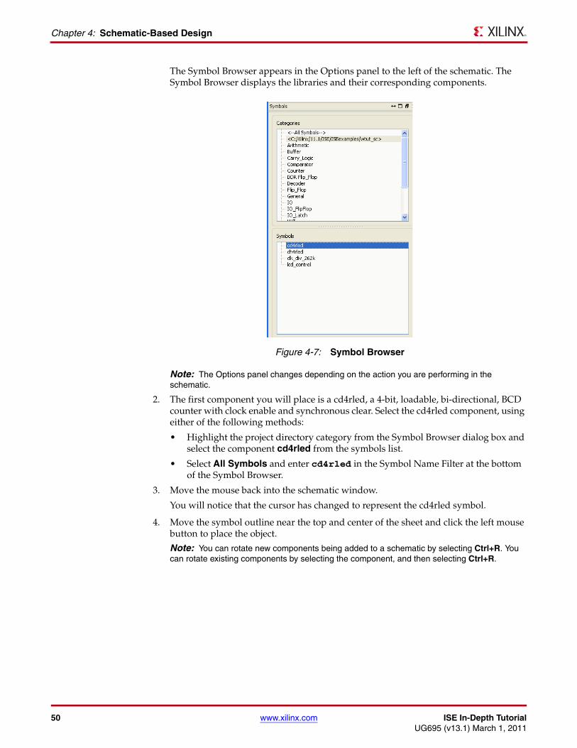
50 www.xilinx.com ISE In-Depth TutorialUG695 (v13.1) March 1, 2011
Chapter 4: Schematic-Based Design
The Symbol Browser appears in the Options panel to the left of the schematic. The Symbol Browser displays the libraries and their corresponding components.
Note: The Options panel changes depending on the action you are performing in the schematic.
2. The first component you will place is a cd4rled, a 4-bit, loadable, bi-directional, BCD counter with clock enable and synchronous clear. Select the cd4rled component, using either of the following methods:
• Highlight the project directory category from the Symbol Browser dialog box and select the component cd4rled from the symbols list.
• Select All Symbols and enter cd4rled in the Symbol Name Filter at the bottom of the Symbol Browser.
3. Move the mouse back into the schematic window.
You will notice that the cursor has changed to represent the cd4rled symbol.
4. Move the symbol outline near the top and center of the sheet and click the left mouse button to place the object.
Note: You can rotate new components being added to a schematic by selecting Ctrl+R. You can rotate existing components by selecting the component, and then selecting Ctrl+R.
X-Ref Target - Figure 4-7
Figure 4-7: Symbol Browser
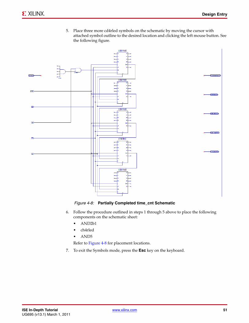
ISE In-Depth Tutorial www.xilinx.com 51UG695 (v13.1) March 1, 2011
Design Entry
5. Place three more cd4rled symbols on the schematic by moving the cursor with attached symbol outline to the desired location and clicking the left mouse button. See the following figure.
6. Follow the procedure outlined in steps 1 through 5 above to place the following components on the schematic sheet:
• AND2b1
• ch4rled
• AND5
Refer to Figure 4-8 for placement locations.
7. To exit the Symbols mode, press the Esc key on the keyboard.
X-Ref Target - Figure 4-8
Figure 4-8: Partially Completed time_cnt Schematic
52 www.xilinx.com ISE In-Depth TutorialUG695 (v13.1) March 1, 2011
Chapter 4: Schematic-Based Design
For a detailed description of the functionality of Xilinx library components, right-click the component and select Object Properties. In the Object Properties dialog box, select Symbol Info. Symbol information is also available in the Libraries Guides. These guides are available from the ISE Software Manuals collection, automatically installed with your ISE software. To open the Software Manuals collection, select Help > Software Manuals. The Software Manuals collection is also available from the Xilinx website.
Correcting Mistakes
If you make a mistake when placing a component, you can easily move or delete the component as follows:
• To move the component, click the component and drag the mouse around the window.
• To delete a placed component, use either of the following methods:
• Click the component, and press the Delete key on your keyboard.
• Right-click the component, and select Delete.
Drawing Wires
You can draw wires (also called nets) to connect the components placed in the schematic. Perform the following steps to draw a net between the AND2b1 and top cd4rled components on the time_cnt schematic:
1. Select Add > Wire, or click the Add Wire toolbar button.
2. Click the output pin of the AND2b1 and then click the destination pin CE on the cd4rled component. The Schematic Editor draws a net between the two pins.
3. Draw a net to connect the output of the AND5 component to the inverted input of the AND2b1 component. Connect the other input of the AND2b1 to the ce input I/O marker.
4. Connect the load, up, clk, and clr input I/O markers respectively to the L, UP, C, and R pins of each of the five counter blocks and connect the CEO pin of the first four counters to the CE pin of the next counter as shown in Figure 4-8.
To specify the shape of the net, do the following:
1. Move the mouse in the direction you want to draw the net.
2. Click the mouse to create a 90-degree bend in the wire.
Note: To draw a net between an already existing net and a pin, click once on the component pin and once on the existing net. A junction point is drawn on the existing net.
Adding Buses
In the Schematic Editor, a bus is simply a wire that has been given a multi-bit name. To add a bus, use the methodology for adding wires and then add a multi-bit name. After a bus has been created, you have the option of “tapping” this bus off to use each signal individually.
X-Ref Target - Figure 4-9
Figure 4-9: Add Wire Toolbar Button
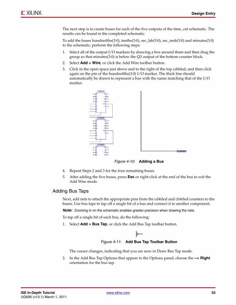
ISE In-Depth Tutorial www.xilinx.com 53UG695 (v13.1) March 1, 2011
Design Entry
The next step is to create buses for each of the five outputs of the time_cnt schematic. The results can be found in the completed schematic.
To add the buses hundredths(3:0), tenths(3:0), sec_lsb(3:0), sec_msb(3:0) and minutes(3:0) to the schematic, perform the following steps:
1. Select all of the output I/O markers by drawing a box around them and then drag the group so that minutes(3:0) is below the Q3 output of the bottom counter block.
2. Select Add > Wire, or click the Add Wire toolbar button.
3. Click in the open space just above and to the right of the top cd4rled, and then click again on the pin of the hundredths(3:0) I/O marker. The thick line should automatically be drawn to represent a bus with the name matching that of the I/O marker.
4. Repeat Steps 2 and 3 for the four remaining buses.
5. After adding the five buses, press Esc or right-click at the end of the bus to exit the Add Wire mode.
Adding Bus Taps
Next, add nets to attach the appropriate pins from the cd4rled and ch4rled counters to the buses. Use bus taps to tap off a single bit of a bus and connect it to another component.
Note: Zooming in on the schematic enables greater precision when drawing the nets.
To tap off a single bit of each bus, do the following:
1. Select Add > Bus Tap, or click the Add Bus Tap toolbar button.
The cursor changes, indicating that you are now in Draw Bus Tap mode.
2. In the Add Bus Tap Options that appear in the Options panel, choose the --< Right orientation for the bus tap.
X-Ref Target - Figure 4-10
Figure 4-10: Adding a Bus
X-Ref Target - Figure 4-11
Figure 4-11: Add Bus Tap Toolbar Button
54 www.xilinx.com ISE In-Depth TutorialUG695 (v13.1) March 1, 2011
Chapter 4: Schematic-Based Design
3. Click on the hundreths(3:0) bus with the center bar of the cursor.
The Selected Bus Name and the Net Name values in the Options panel are now populated.
Note: The indexes of the Net Name may be incremented or decremented by clicking the arrow buttons next to the Net Name box.
4. With hundredths(3) as the Net Name value, move the cursor so the tip of the attached tap touches the Q3 pin of the top cd4rled component.
Note: Four selection squares appear around the pin when the cursor is in the correct position.
5. Click once when the cursor is in the correct position.
A tap is connected to the hundredths(3:0) bus, and a wire named hundreths(3) is drawn between the tap and the Q3 pin.
Click successively on pins Q2, Q1, and Q0 to create taps for the remaining bits of the hundredths(3:0) bus.
6. Repeat Steps 3 to 5 to tap off four bits from each of the five buses.
Note: It is the name of the wire that makes the electrical connection between the bus and the wire (for example, sec_msb(2) connects to the third bit of sec(3:0)). The bus tap figure is for visual purposes only. The following section shows additional electrical connections by name association.
7. Press Esc to exit the Add Bus Tap mode.
8. Compare your time_cnt schematic with Figure 4-13 to ensure that all connections are made properly.
Adding Net Names
First, add a hanging wire to each of the five inputs of the AND5 component and to the TC pin of each of the counter blocks.
Next, add net names to the wires. To add the net names, do the following:
1. Select Add > Net Name, or click the Add Net Name toolbar button.
2. In the Add Net Name Options that appear in the Options panel, do the following:
a. In the Name field, enter tc_out0.
b. Select Increase the Name.
The net name tc_out0 is now attached to the cursor.
3. Click the net attached to the first input of the AND5 component.
The name is attached to the net. The net name appears above the net if the name is placed on any point of the net other than an end point.
4. Click on the remaining input nets of the AND5 to add tc_out1, tc_out2, tc_out3 and tc_out4.
The Schematic Editor increments the net name as each name is placed on a net.
Note: Alternatively, name the first net tc_out4 and select Decrease the name in the Add Net Names Options, and nets are named from the bottom up.
X-Ref Target - Figure 4-12
Figure 4-12: Add Net Name Toolbar Button
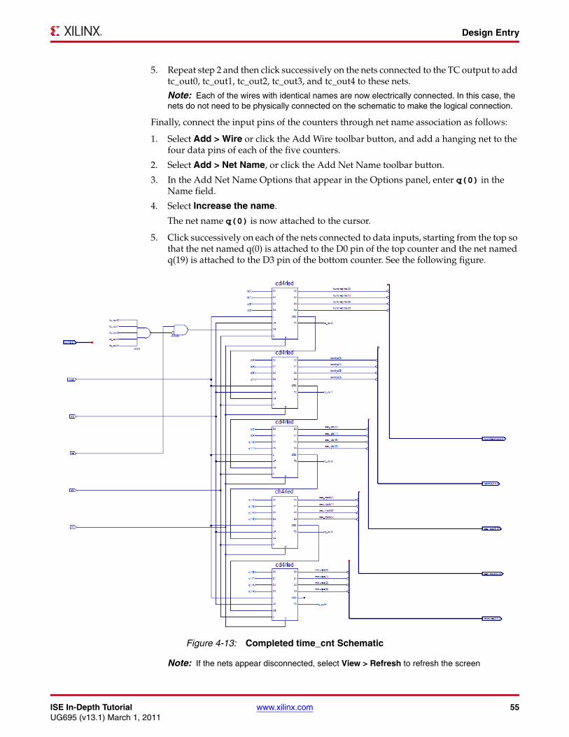
ISE In-Depth Tutorial www.xilinx.com 55UG695 (v13.1) March 1, 2011
Design Entry
5. Repeat step 2 and then click successively on the nets connected to the TC output to add tc_out0, tc_out1, tc_out2, tc_out3, and tc_out4 to these nets.
Note: Each of the wires with identical names are now electrically connected. In this case, the nets do not need to be physically connected on the schematic to make the logical connection.
Finally, connect the input pins of the counters through net name association as follows:
1. Select Add > Wire or click the Add Wire toolbar button, and add a hanging net to the four data pins of each of the five counters.
2. Select Add > Net Name, or click the Add Net Name toolbar button.
3. In the Add Net Name Options that appear in the Options panel, enter q(0) in the Name field.
4. Select Increase the name.
The net name q(0) is now attached to the cursor.
5. Click successively on each of the nets connected to data inputs, starting from the top so that the net named q(0) is attached to the D0 pin of the top counter and the net named q(19) is attached to the D3 pin of the bottom counter. See the following figure.
Note: If the nets appear disconnected, select View > Refresh to refresh the screen
X-Ref Target - Figure 4-13
Figure 4-13: Completed time_cnt Schematic
56 www.xilinx.com ISE In-Depth TutorialUG695 (v13.1) March 1, 2011
Chapter 4: Schematic-Based Design
Checking the Schematic
The time_cnt schematic is now complete. Verify that the schematic does not contain logical errors by running a design rule check (DRC). To do this, select Tools > Check Schematic. The Console should report that no errors or warnings are detected. If an error or warning is displayed, fix the reported problem before proceeding.
Saving the Schematic
Save the schematic as follows:
1. Select File > Save, or click the Save toolbar button.
2. Close the time_cnt schematic.
Creating and Placing the time_cnt SymbolThe next step is to create a “symbol” that represents the time_cnt macro. The symbol is an instantiation of the macro. After you create a symbol for time_cnt, you will add the symbol to a top-level schematic of the stopwatch design. In the top-level schematic, the symbol of the time_cnt macro will be connected to other components in a later section in this chapter.
Creating the time_cnt Symbol
You can create a symbol using either a Project Navigator process or a Tools menu command.
To create a symbol that represents the time_cnt schematic using a Project Navigator process, do the following:
1. In the Hierarchy pane of the Design panel, select time_cnt.sch.
2. In the Processes pane, expand Design Utilities, and double-click Create Schematic Symbol.
To create a symbol that represents the time_cnt schematic using a Tools menu command, do the following:
1. With the time_cnt schematic sheet open, select Tools > Symbol Wizard.
2. In the Symbol Wizard, select Using Schematic, and select time_cnt.
3. Click Next, then Next, then Next, and then Finish to use the wizard defaults.
4. View and then close the time_cnt symbol.
X-Ref Target - Figure 4-14
Figure 4-14: Save Toolbar Button
ISE In-Depth Tutorial www.xilinx.com 57UG695 (v13.1) March 1, 2011
Design Entry
Placing the time_cnt Symbol
Next, place the symbol that represents the macro on the top-level schematic (stopwatch.sch) as follows:
1. In the Hierarchy pane of the Design panel, double-click stopwatch.sch to open the schematic.
2. Select Add > Symbol, or click the Add Symbol toolbar button.
3. In the Symbol Browser, select the local symbols library (c:\xilinx_tutorial\wtut_sc), and then select the newly created time_cnt symbol.
4. Place the time_cnt symbol in the schematic so that the output pins line up with the five buses driving inputs to the lcd_control component. This should be close to grid position [1612,1728]. Grid position is shown at the bottom right corner of the Project Navigator window, and is updated as the cursor is moved around the schematic.
Note: Do not worry about connecting nets to the input pins of the time_cnt symbol. You will do this after adding other components to the stopwatch schematic.
5. Save the changes and close stopwatch.sch.
Creating a CORE Generator Software ModuleThe CORE Generator software is a graphical interactive design tool that enables you to create high-level modules such as memory elements, math functions, communications, and I/O interface cores. You can customize and pre-optimize the modules to take advantage of the inherent architectural features of the Xilinx FPGA architectures, such as Fast Carry Logic, SRL16s, and distributed and block RAM.
In this section, you will create a CORE Generator software module called timer_preset. The module is used to store a set of 64 values to load into the timer.
Creating the timer_preset CORE Generator Software Module
To create a CORE Generator software module, do the following:
1. In Project Navigator, select Project > New Source.
2. Select IP (Coregen & Architecture Wizard).
3. In the File name field, enter timer_preset.
4. Click Next.
5. Double-click Memories & Storage Elements > RAMs & ROMs.
X-Ref Target - Figure 4-15
Figure 4-15: Add Symbol Toolbar Button
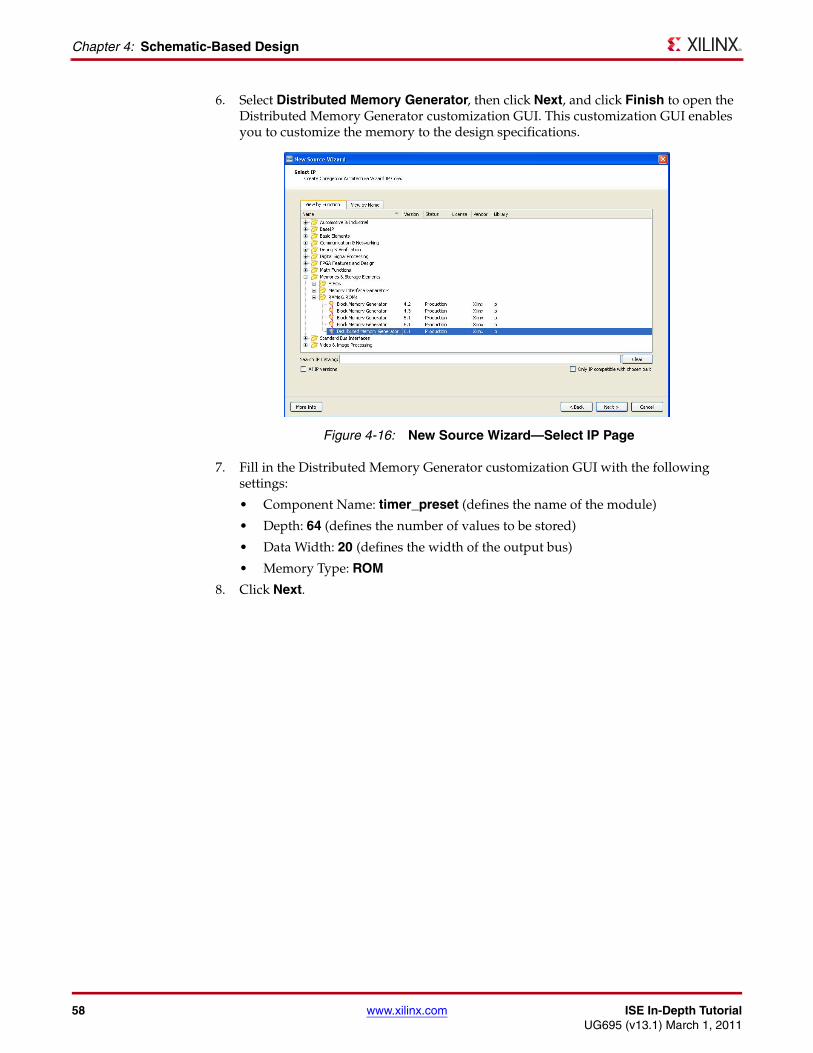
58 www.xilinx.com ISE In-Depth TutorialUG695 (v13.1) March 1, 2011
Chapter 4: Schematic-Based Design
6. Select Distributed Memory Generator, then click Next, and click Finish to open the Distributed Memory Generator customization GUI. This customization GUI enables you to customize the memory to the design specifications.
7. Fill in the Distributed Memory Generator customization GUI with the following settings:
• Component Name: timer_preset (defines the name of the module)
• Depth: 64 (defines the number of values to be stored)
• Data Width: 20 (defines the width of the output bus)
• Memory Type: ROM
8. Click Next.
X-Ref Target - Figure 4-16
Figure 4-16: New Source Wizard—Select IP Page
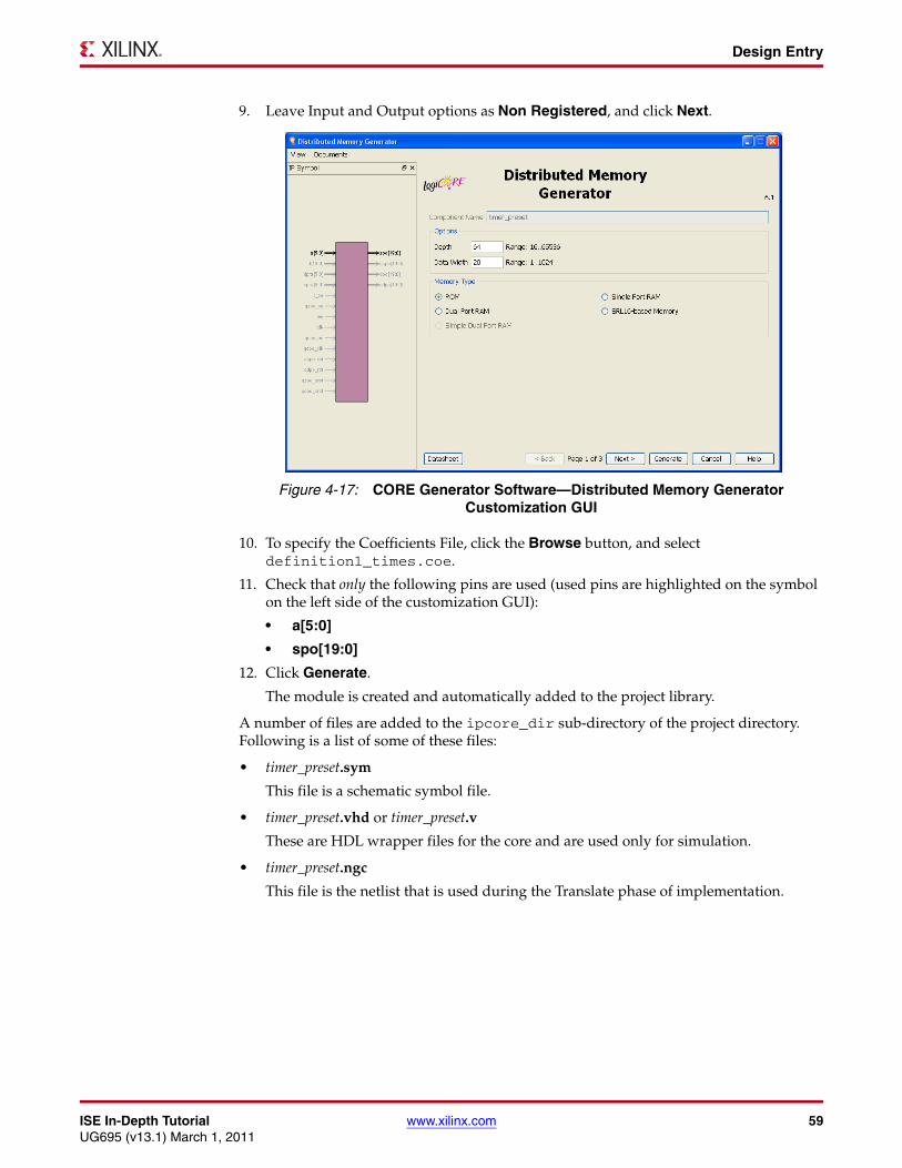
ISE In-Depth Tutorial www.xilinx.com 59UG695 (v13.1) March 1, 2011
Design Entry
9. Leave Input and Output options as Non Registered, and click Next.
10. To specify the Coefficients File, click the Browse button, and select definition1_times.coe.
11. Check that only the following pins are used (used pins are highlighted on the symbol on the left side of the customization GUI):
• a[5:0]
• spo[19:0]
12. Click Generate.
The module is created and automatically added to the project library.
A number of files are added to the ipcore_dir sub-directory of the project directory. Following is a list of some of these files:
• timer_preset.sym
This file is a schematic symbol file.
• timer_preset.vhd or timer_preset.v
These are HDL wrapper files for the core and are used only for simulation.
• timer_preset.ngc
This file is the netlist that is used during the Translate phase of implementation.
X-Ref Target - Figure 4-17
Figure 4-17: CORE Generator Software—Distributed Memory Generator Customization GUI
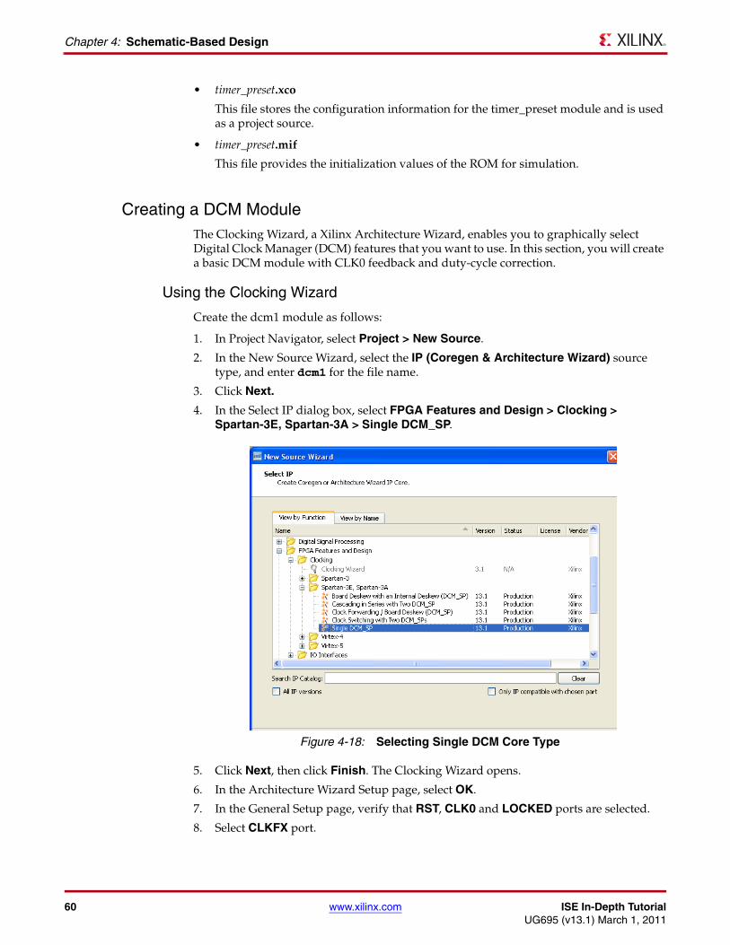
60 www.xilinx.com ISE In-Depth TutorialUG695 (v13.1) March 1, 2011
Chapter 4: Schematic-Based Design
• timer_preset.xco
This file stores the configuration information for the timer_preset module and is used as a project source.
• timer_preset.mif
This file provides the initialization values of the ROM for simulation.
Creating a DCM ModuleThe Clocking Wizard, a Xilinx Architecture Wizard, enables you to graphically select Digital Clock Manager (DCM) features that you want to use. In this section, you will create a basic DCM module with CLK0 feedback and duty-cycle correction.
Using the Clocking Wizard
Create the dcm1 module as follows:
1. In Project Navigator, select Project > New Source.
2. In the New Source Wizard, select the IP (Coregen & Architecture Wizard) source type, and enter dcm1 for the file name.
3. Click Next.
4. In the Select IP dialog box, select FPGA Features and Design > Clocking > Spartan-3E, Spartan-3A > Single DCM_SP.
5. Click Next, then click Finish. The Clocking Wizard opens.
6. In the Architecture Wizard Setup page, select OK.
7. In the General Setup page, verify that RST, CLK0 and LOCKED ports are selected.
8. Select CLKFX port.
X-Ref Target - Figure 4-18
Figure 4-18: Selecting Single DCM Core Type
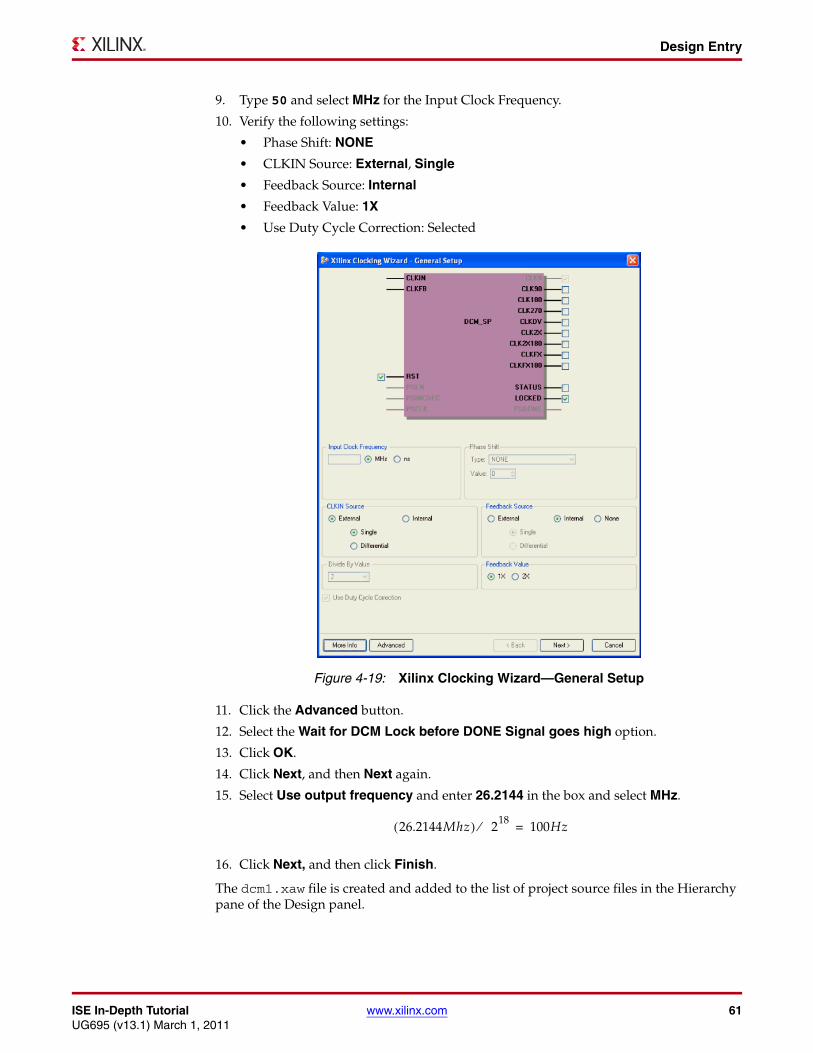
ISE In-Depth Tutorial www.xilinx.com 61UG695 (v13.1) March 1, 2011
Design Entry
9. Type 50 and select MHz for the Input Clock Frequency.
10. Verify the following settings:
• Phase Shift: NONE
• CLKIN Source: External, Single
• Feedback Source: Internal
• Feedback Value: 1X
• Use Duty Cycle Correction: Selected
11. Click the Advanced button.
12. Select the Wait for DCM Lock before DONE Signal goes high option.
13. Click OK.
14. Click Next, and then Next again.
15. Select Use output frequency and enter 26.2144 in the box and select MHz.
16. Click Next, and then click Finish.
The dcm1.xaw file is created and added to the list of project source files in the Hierarchy pane of the Design panel.
X-Ref Target - Figure 4-19
Figure 4-19: Xilinx Clocking Wizard—General Setup
26.2144Mhz( ) 218⁄ 100Hz=
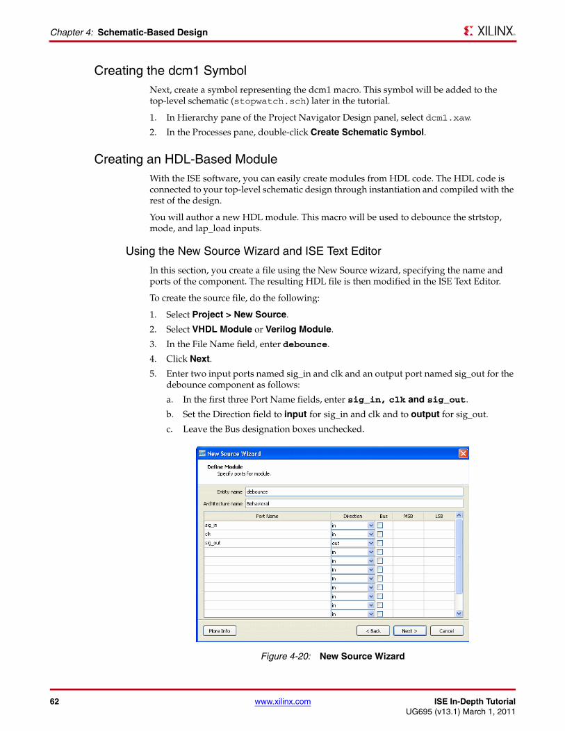
62 www.xilinx.com ISE In-Depth TutorialUG695 (v13.1) March 1, 2011
Chapter 4: Schematic-Based Design
Creating the dcm1 SymbolNext, create a symbol representing the dcm1 macro. This symbol will be added to the top-level schematic (stopwatch.sch) later in the tutorial.
1. In Hierarchy pane of the Project Navigator Design panel, select dcm1.xaw.
2. In the Processes pane, double-click Create Schematic Symbol.
Creating an HDL-Based ModuleWith the ISE software, you can easily create modules from HDL code. The HDL code is connected to your top-level schematic design through instantiation and compiled with the rest of the design.
You will author a new HDL module. This macro will be used to debounce the strtstop, mode, and lap_load inputs.
Using the New Source Wizard and ISE Text Editor
In this section, you create a file using the New Source wizard, specifying the name and ports of the component. The resulting HDL file is then modified in the ISE Text Editor.
To create the source file, do the following:
1. Select Project > New Source.
2. Select VHDL Module or Verilog Module.
3. In the File Name field, enter debounce.
4. Click Next.
5. Enter two input ports named sig_in and clk and an output port named sig_out for the debounce component as follows:
a. In the first three Port Name fields, enter sig_in, clk and sig_out.
b. Set the Direction field to input for sig_in and clk and to output for sig_out.
c. Leave the Bus designation boxes unchecked.X-Ref Target - Figure 4-20
Figure 4-20: New Source Wizard
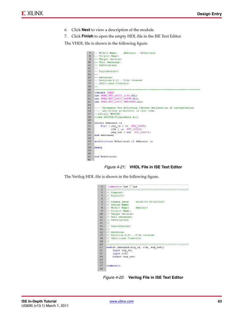
ISE In-Depth Tutorial www.xilinx.com 63UG695 (v13.1) March 1, 2011
Design Entry
6. Click Next to view a description of the module.
7. Click Finish to open the empty HDL file in the ISE Text Editor.
The VHDL file is shown in the following figure.
The Verilog HDL file is shown in the following figure.
X-Ref Target - Figure 4-21
Figure 4-21: VHDL File in ISE Text Editor
X-Ref Target - Figure 4-22
Figure 4-22: Verilog File in ISE Text Editor
64 www.xilinx.com ISE In-Depth TutorialUG695 (v13.1) March 1, 2011
Chapter 4: Schematic-Based Design
In the ISE Text Editor, the ports are already declared in the HDL file, and some of the basic file structure is already in place. Keywords are displayed in blue, comments in green, and values are black. The file is color-coded to enhance readability and help you recognize typographical errors.
Using the Language Templates
The ISE Language Templates include HDL constructs and synthesis templates which represent commonly used logic components, such as counters, D flip-flops, multiplexers, and primitives. You will use the Debounce Circuit template for this exercise.
Note: You can add your own templates to the Language Templates for components or constructs that you use often.
To invoke the Language Templates and select the template for this tutorial, do the following:
1. From Project Navigator, select Edit > Language Templates.
Each HDL language in the Language Templates is divided into the following sections: Common Constructs, Device Macro Instantiation, Device Primitive Instantiation, Simulation Constructs, Synthesis Constructs, and User Templates. To expand the view of any of these sections, click the plus symbol (+) next to the section. Click any of the listed templates to view the template contents in the right pane.
2. Under either the VHDL or Verilog hierarchy, expand Synthesis Constructs, expand Coding Examples, expand Misc, and select the template called Debounce Circuit. Use the appropriate template for the language you are using.
When the template is selected in the hierarchy, the contents display in the right pane.X-Ref Target - Figure 4-23
Figure 4-23: Language Templates
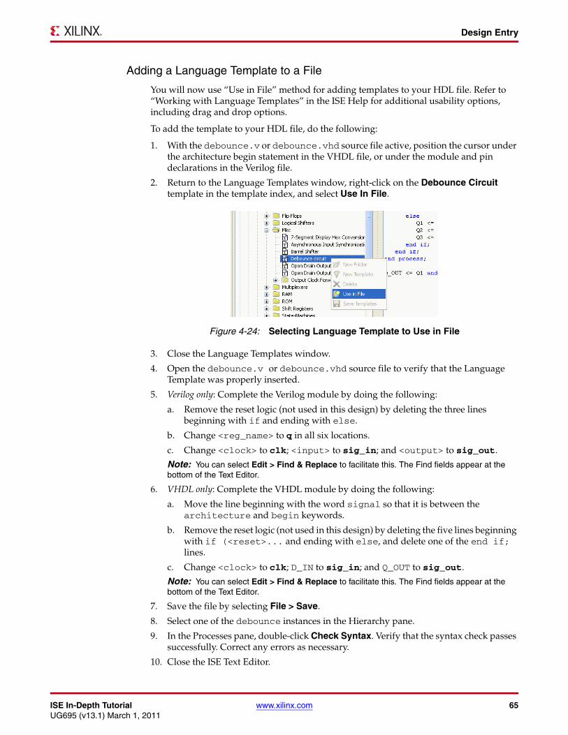
ISE In-Depth Tutorial www.xilinx.com 65UG695 (v13.1) March 1, 2011
Design Entry
Adding a Language Template to a File
You will now use “Use in File” method for adding templates to your HDL file. Refer to “Working with Language Templates” in the ISE Help for additional usability options, including drag and drop options.
To add the template to your HDL file, do the following:
1. With the debounce.v or debounce.vhd source file active, position the cursor under the architecture begin statement in the VHDL file, or under the module and pin declarations in the Verilog file.
2. Return to the Language Templates window, right-click on the Debounce Circuit template in the template index, and select Use In File.
3. Close the Language Templates window.
4. Open the debounce.v or debounce.vhd source file to verify that the Language Template was properly inserted.
5. Verilog only: Complete the Verilog module by doing the following:
a. Remove the reset logic (not used in this design) by deleting the three lines beginning with if and ending with else.
b. Change <reg_name> to q in all six locations.
c. Change <clock> to clk; <input> to sig_in; and <output> to sig_out.
Note: You can select Edit > Find & Replace to facilitate this. The Find fields appear at the bottom of the Text Editor.
6. VHDL only: Complete the VHDL module by doing the following:
a. Move the line beginning with the word signal so that it is between the architecture and begin keywords.
b. Remove the reset logic (not used in this design) by deleting the five lines beginning with if (<reset>... and ending with else, and delete one of the end if; lines.
c. Change <clock> to clk; D_IN to sig_in; and Q_OUT to sig_out.
Note: You can select Edit > Find & Replace to facilitate this. The Find fields appear at the bottom of the Text Editor.
7. Save the file by selecting File > Save.
8. Select one of the debounce instances in the Hierarchy pane.
9. In the Processes pane, double-click Check Syntax. Verify that the syntax check passes successfully. Correct any errors as necessary.
10. Close the ISE Text Editor.
X-Ref Target - Figure 4-24
Figure 4-24: Selecting Language Template to Use in File
66 www.xilinx.com ISE In-Depth TutorialUG695 (v13.1) March 1, 2011
Chapter 4: Schematic-Based Design
Creating Schematic Symbols for HDL ModulesNext, create the schematic symbols for both the debounce and statmach HDL files as follows:
1. In the Hierarchy pane of the Project Navigator Design panel, select debounce.vhd or debounce.v.
2. In the Processes panel, expand Design Utilities, and double-click Create Schematic Symbol.
3. Repeat this procedure for the statmach.vhd file.
You are now ready to place the symbols on the stopwatch schematic.
Placing the statmach, timer_preset, dcm1, and debounce SymbolsYou can now place the statmach, timer_preset, dcm1, and debounce symbols on the stopwatch schematic (stopwatch.sch).
To place the symbols, do the following:
1. In the Hierarchy pane of the Project Navigator Design panel, double-click stopwatch.sch.
The schematic file opens in the Workspace
2. Select Add > Symbol, or click the Add Symbol toolbar button.
The Symbol Browser appears in the Options panel to the left of the schematic. The Symbol Browser displays the libraries and their corresponding components.
3. View the list of available library components in the Symbol Browser.
4. Locate the project-specific macros by selecting the project directory name in the Categories window.
Note: The timer_preset symbol is located in the ipcore_dir directory.
5. Select the appropriate symbol, and add it to the stopwatch schematic in the approximate location, as shown in Figure 4-26.
Note: Do not worry about drawing the wires to connect the symbols. You will connect components in the schematic later in the tutorial.
6. Save the schematic.
X-Ref Target - Figure 4-25
Figure 4-25: Add Symbol Toolbar Button
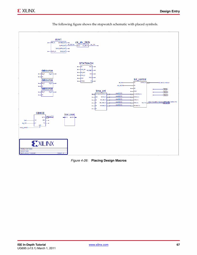
ISE In-Depth Tutorial www.xilinx.com 67UG695 (v13.1) March 1, 2011
Design Entry
The following figure shows the stopwatch schematic with placed symbols.X-Ref Target - Figure 4-26
Figure 4-26: Placing Design Macros
68 www.xilinx.com ISE In-Depth TutorialUG695 (v13.1) March 1, 2011
Chapter 4: Schematic-Based Design
Changing Instance NamesWhen a symbol is placed on a schematic sheet, it is given a unique instance name beginning with the prefix XLXI_. To help make the hierarchy more readable in the Project Navigator Hierarchy pane, change the names of the added symbol instances as follows:
1. Right-click on the dcm1 symbol instance, and select Object Properties.
2. In the Object Properties dialog box, change the value of the InstName field to dcm_inst, and click OK.
3. Repeat steps 1 and 2 to change the following symbol instance names:
• Name the statmach instance timer_state.
• Name the top debounce instance lap_load_debounce.
• Name the middle debounce instance mode_debounce.
• Name the bottom debounce instance strtstop_debounce.
• Name the timer_preset instance t_preset.
• Name the time_cnt instance timer_cnt.
Using Hierarchy Push/PopFirst, perform a hierarchy “push down,” which enables you to focus in on a lower-level of the schematic hierarchy to view the underlying file. Push down into the time_cnt macro, which is a schematic-based macro created earlier in this tutorial, and examine its components.
To push down into time_cnt from the top-level stopwatch schematic, do the following:
1. Click time_cnt symbol in the schematic, and select the Hierarchy Push toolbar button. You can also right-click the macro, and select Symbol > Push into Symbol.
In the time_cnt schematic, you see five counter blocks. Push into any of the counter blocks by selecting the block and clicking on the Hierarchy Push toolbar button. This process may be repeated until the schematic page contains only Xilinx primitive components. If you push into a symbol that has an underlying HDL or IP core file, the appropriate text editor or customization GUI opens, which enables you to edit the file.
2. After examining the macro, return to the top-level schematic by selecting View > Pop to Calling Schematic, or select the Hierarchy Pop toolbar button when nothing in the schematic is selected. You can also right-click in an open space of the schematic, and select Pop to Calling Schematic.
X-Ref Target - Figure 4-27
Figure 4-27: Hierarchy Push Toolbar Button
X-Ref Target - Figure 4-28
Figure 4-28: Hierarchy Pop Toolbar Button
ISE In-Depth Tutorial www.xilinx.com 69UG695 (v13.1) March 1, 2011
Design Entry
Specifying Device Inputs/OutputsUse the I/O marker to specify device I/O on a schematic sheet. All of the Schematic Editor schematics are netlisted to VHDL or Verilog and then synthesized by the synthesis tool of choice. When the synthesis tool synthesizes the top-level schematic HDL, the I/O markers are replaced with the appropriate pads and buffers.
Adding Input Pins
Next, add five input pins to the stopwatch schematic: reset, clk, lap_load, mode and strtstop.
To add these components, draw a hanging wire to the two inputs of dcm1 and to the sig_in pin of each debounce symbol.
Note: Refer to Drawing Wires for detailed instructions.
Adding I/O Markers and Net Names
It is important to label nets and buses for the following reasons:
• Aids in debugging and simulation, because you can more easily trace nets back to your original design.
For example, any nets that remain unnamed in the design will be given generated names that will mean nothing to you later in the implementation process.
• Enhances readability and aids in documenting your design.
Label the five input nets you just drew. Refer to the completed schematic below. To label the reset net, do the following:
1. Select Add > Net Name.
2. In the Add Net Name Options that appear in the Options panel, enter reset in the Name box.
The net name is now attached to the cursor.
3. Place the name on the leftmost end of the net, as shown in Figure 4-29.
4. Repeat Steps 1 through 3 for the clk, lap_load, mode, and strtstop pins.
After all of the nets have been labeled, add the I/O marker.
5. Select Add > I/O Marker.
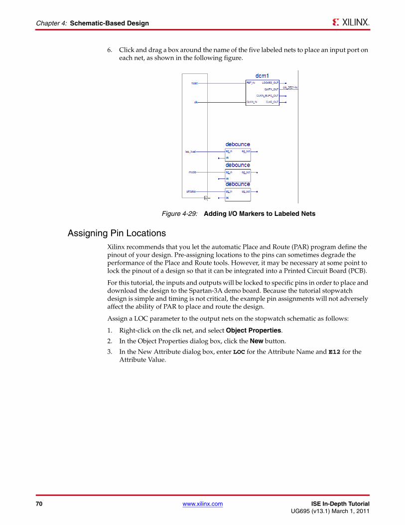
70 www.xilinx.com ISE In-Depth TutorialUG695 (v13.1) March 1, 2011
Chapter 4: Schematic-Based Design
6. Click and drag a box around the name of the five labeled nets to place an input port on each net, as shown in the following figure.
Assigning Pin LocationsXilinx recommends that you let the automatic Place and Route (PAR) program define the pinout of your design. Pre-assigning locations to the pins can sometimes degrade the performance of the Place and Route tools. However, it may be necessary at some point to lock the pinout of a design so that it can be integrated into a Printed Circuit Board (PCB).
For this tutorial, the inputs and outputs will be locked to specific pins in order to place and download the design to the Spartan-3A demo board. Because the tutorial stopwatch design is simple and timing is not critical, the example pin assignments will not adversely affect the ability of PAR to place and route the design.
Assign a LOC parameter to the output nets on the stopwatch schematic as follows:
1. Right-click on the clk net, and select Object Properties.
2. In the Object Properties dialog box, click the New button.
3. In the New Attribute dialog box, enter LOC for the Attribute Name and E12 for the Attribute Value.
X-Ref Target - Figure 4-29
Figure 4-29: Adding I/O Markers to Labeled Nets
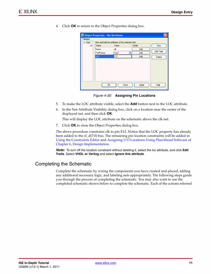
ISE In-Depth Tutorial www.xilinx.com 71UG695 (v13.1) March 1, 2011
Design Entry
4. Click OK to return to the Object Properties dialog box.
5. To make the LOC attribute visible, select the Add button next to the LOC attribute.
6. In the Net Attribute Visibility dialog box, click on a location near the center of the displayed net, and then click OK.
This will display the LOC attribute on the schematic above the clk net.
7. Click OK to close the Object Properties dialog box.
The above procedure constrains clk to pin E12. Notice that the LOC property has already been added to the sf_d(7:0) bus. The remaining pin location constraints will be added in Using the Constraints Editor and Assigning I/O Locations Using PlanAhead Software of Chapter 6, Design Implementation.
Note: To turn off the location constraint without deleting it, select the loc attribute, and click Edit Traits. Select VHDL or Verilog and select Ignore this attribute.
Completing the SchematicComplete the schematic by wiring the components you have created and placed, adding any additional necessary logic, and labeling nets appropriately. The following steps guide you through the process of completing the schematic. You may also want to use the completed schematic shown below to complete the schematic. Each of the actions referred
X-Ref Target - Figure 4-30
Figure 4-30: Assigning Pin Locations
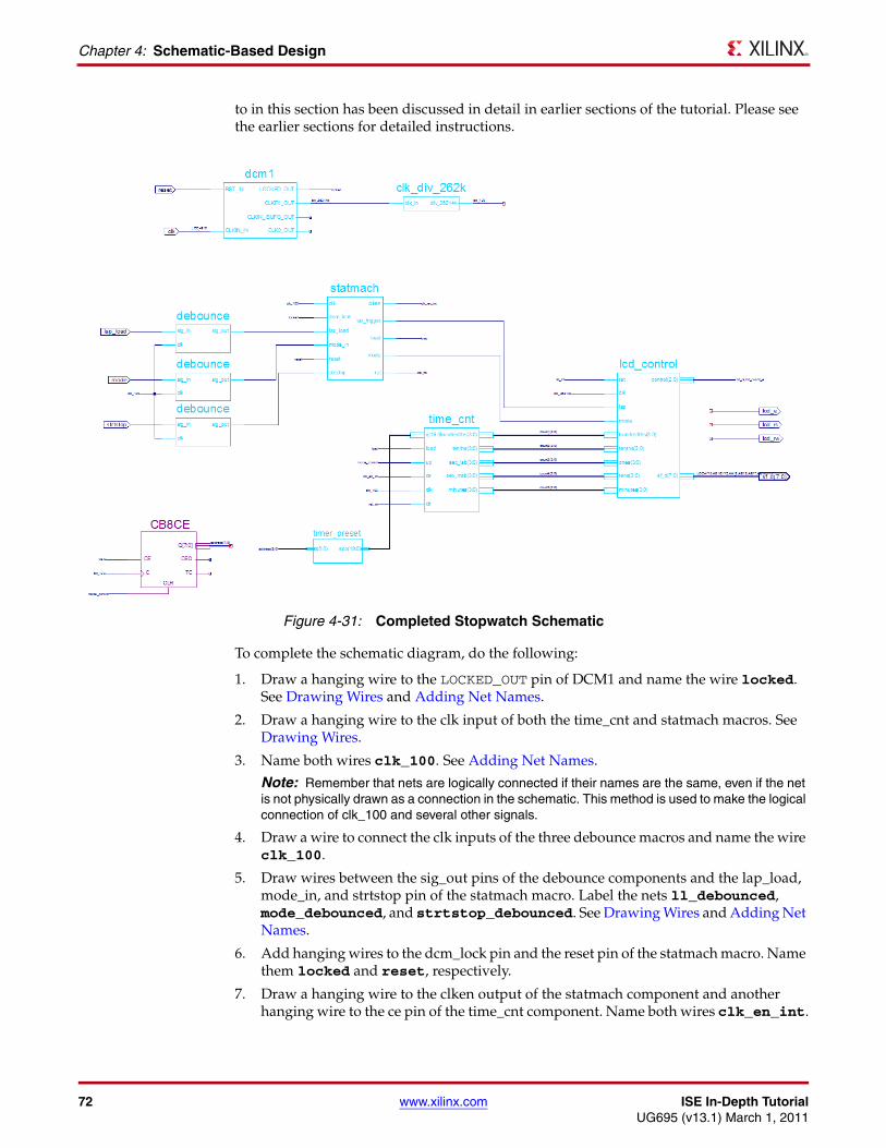
72 www.xilinx.com ISE In-Depth TutorialUG695 (v13.1) March 1, 2011
Chapter 4: Schematic-Based Design
to in this section has been discussed in detail in earlier sections of the tutorial. Please see the earlier sections for detailed instructions.
To complete the schematic diagram, do the following:
1. Draw a hanging wire to the LOCKED_OUT pin of DCM1 and name the wire locked. See Drawing Wires and Adding Net Names.
2. Draw a hanging wire to the clk input of both the time_cnt and statmach macros. See Drawing Wires.
3. Name both wires clk_100. See Adding Net Names.
Note: Remember that nets are logically connected if their names are the same, even if the net is not physically drawn as a connection in the schematic. This method is used to make the logical connection of clk_100 and several other signals.
4. Draw a wire to connect the clk inputs of the three debounce macros and name the wire clk_100.
5. Draw wires between the sig_out pins of the debounce components and the lap_load, mode_in, and strtstop pin of the statmach macro. Label the nets ll_debounced, mode_debounced, and strtstop_debounced. See Drawing Wires and Adding Net Names.
6. Add hanging wires to the dcm_lock pin and the reset pin of the statmach macro. Name them locked and reset, respectively.
7. Draw a hanging wire to the clken output of the statmach component and another hanging wire to the ce pin of the time_cnt component. Name both wires clk_en_int.
X-Ref Target - Figure 4-31
Figure 4-31: Completed Stopwatch Schematic
ISE In-Depth Tutorial www.xilinx.com 73UG695 (v13.1) March 1, 2011
Design Entry
8. Draw hanging wires from the rst output pin of the statmach macro and the clr pin of the time_cnt macro. See Drawing Wires. Label both wires rst_int.
9. Draw a wire from the bus output of the timer_preset to the q(19:0) input of the time_cnt macro. See Drawing Wires. Notice how the wire is automatically converted to a bus.
10. Draw a hanging bus on the input of the timer_preset macro and name the bus address(5:0).
11. Draw wires from the lap_trigger and mode outputs of the statmach macro to the lap and mode inputs of the lcd_control macro. See Drawing Wires. Name the nets lap and mode_control respectively.
12. Draw hanging wires from the load output of the statmach macro and the load input of the time_cnt macro. See Drawing Wires. Name both wires load.
13. Draw a hanging wire to the up input time_cnt macro. See Drawing Wires. Name the wire mode_control.
14. Save the design by selecting File > Save.
You have now completed the schematic design.
To continue with the schematic flow, do either of the following:
• Go to Chapter 5, Behavioral Simulation, to perform a pre-synthesis simulation of this design.
• Proceed to Chapter 6, Design Implementation, to place and route the design.

74 www.xilinx.com ISE In-Depth TutorialUG695 (v13.1) March 1, 2011
Chapter 4: Schematic-Based Design
ISE In-Depth Tutorial www.xilinx.com 75UG695 (v13.1) March 1, 2011
Chapter 5
Behavioral Simulation
Overview of Behavioral Simulation FlowThe Xilinx® ISE® Design Suite provides an integrated flow with the Mentor ModelSim simulator and the Xilinx ISim simulator that allows simulations to be run from the Xilinx Project Navigator. The examples in this tutorial demonstrate how to use the integrated flow. Whether you use the ModelSim simulator or the ISim simulator with this tutorial, you will achieve the same simulation results.
For additional information about simulation, and for a list of other supported simulators, see the Synthesis and Simulation Design Guide (UG626). This guide is available from the ISE Software Manuals collection, automatically installed with your ISE software. To open the Software Manuals collection, select Help > Software Manuals. The Software Manuals collection is also available from the Xilinx website.
This tutorial provides an introduction to the simulation flow within Project Navigator, including highlights of features within the ModelSim and ISim simulators. For more detailed information about using these simulators, see the ModelSim documentation available from the ModelSim website or the ISim tutorial provided with the ISE Design Suite Tutorials available from the Xilinx website.
ModelSim SetupTo use this tutorial, you must install ModelSim on your computer. ModelSim PE, ModelSim SE, and ModelSim DE are full versions of ModelSim available for purchase directly from Mentor Graphics. To simulate with the ISE Design Suite libraries, use ModelSim 6.5c or newer. Older versions may work but are not supported. For more information about ModelSim PE, SE, and DE, please contact Mentor Graphics.
ISim SetupISim is automatically installed and set up with the ISE Design Suite installer on supported operating systems. To see a list of operating systems supported by ISim, please see the ISE Design Suite: Release Notes Guide (UG631) available from the Xilinx website.
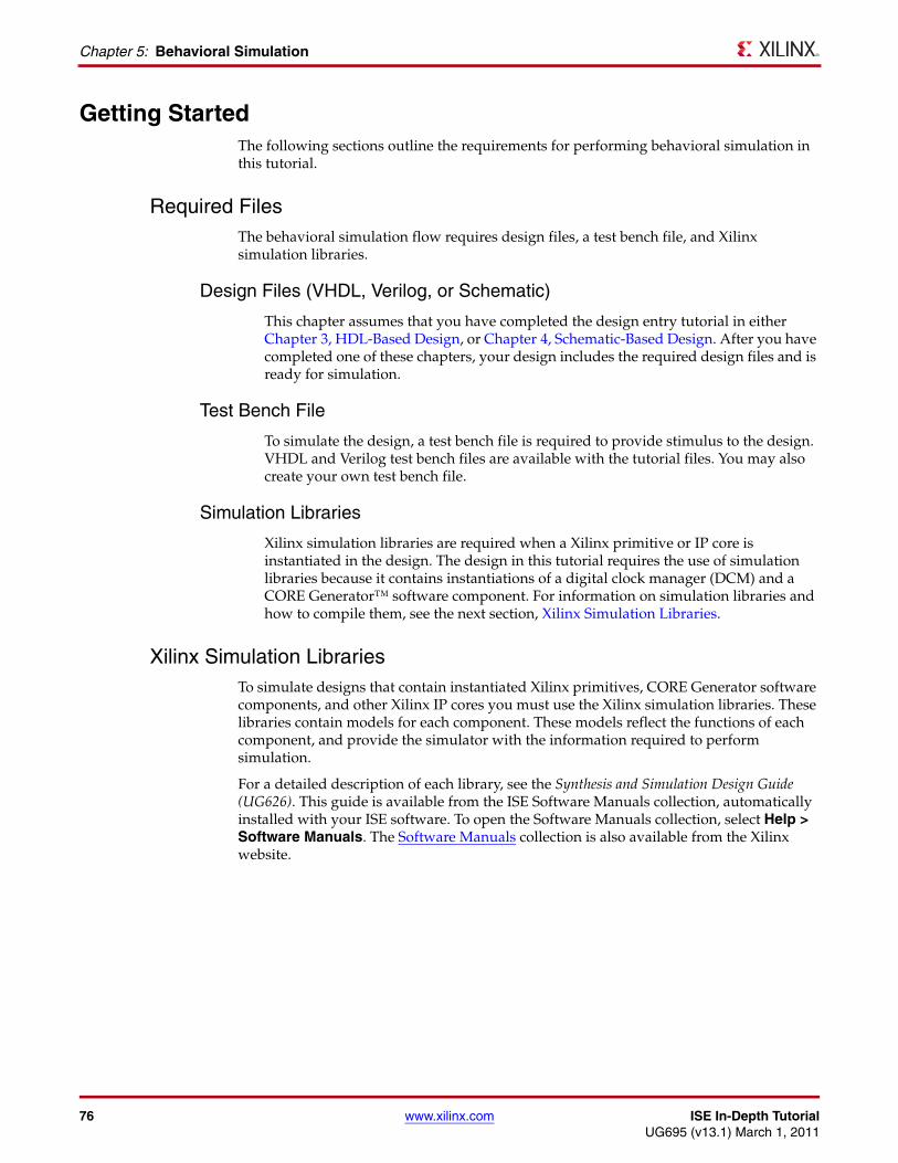
76 www.xilinx.com ISE In-Depth TutorialUG695 (v13.1) March 1, 2011
Chapter 5: Behavioral Simulation
Getting StartedThe following sections outline the requirements for performing behavioral simulation in this tutorial.
Required FilesThe behavioral simulation flow requires design files, a test bench file, and Xilinx simulation libraries.
Design Files (VHDL, Verilog, or Schematic)
This chapter assumes that you have completed the design entry tutorial in either Chapter 3, HDL-Based Design, or Chapter 4, Schematic-Based Design. After you have completed one of these chapters, your design includes the required design files and is ready for simulation.
Test Bench File
To simulate the design, a test bench file is required to provide stimulus to the design. VHDL and Verilog test bench files are available with the tutorial files. You may also create your own test bench file.
Simulation Libraries
Xilinx simulation libraries are required when a Xilinx primitive or IP core is instantiated in the design. The design in this tutorial requires the use of simulation libraries because it contains instantiations of a digital clock manager (DCM) and a CORE Generator™ software component. For information on simulation libraries and how to compile them, see the next section, Xilinx Simulation Libraries.
Xilinx Simulation LibrariesTo simulate designs that contain instantiated Xilinx primitives, CORE Generator software components, and other Xilinx IP cores you must use the Xilinx simulation libraries. These libraries contain models for each component. These models reflect the functions of each component, and provide the simulator with the information required to perform simulation.
For a detailed description of each library, see the Synthesis and Simulation Design Guide (UG626). This guide is available from the ISE Software Manuals collection, automatically installed with your ISE software. To open the Software Manuals collection, select Help > Software Manuals. The Software Manuals collection is also available from the Xilinx website.
ISE In-Depth Tutorial www.xilinx.com 77UG695 (v13.1) March 1, 2011
Getting Started
Updating the Xilinx Simulation Libraries
The Xilinx simulation libraries contain models that are updated on a regular basis:
• XilinxCoreLib models are updated each time an IP Update is installed.
• All other models are updated each time a software update is installed.
When the models are updated, you must recompile the libraries. The compiled Xilinx simulation libraries are then available during the simulation of any design.
ModelSim PE, SE, or DE
If you are using ModelSim PE, SE, or DE, you must compile the simulation libraries with the updated models. See the Synthesis and Simulation Design Guide (UG626). This guide is available from the ISE Software Manuals collection, automatically installed with your ISE software. To open the Software Manuals collection, select Help > Software Manuals. The Software Manuals collection is also available from the Xilinx website.
Xilinx ISim
Updated simulation libraries for ISim are precompiled and installed with ISE software installations.
Mapping Simulation Libraries in the modelsim.ini File
ModelSim uses the modelsim.ini file to determine the location of the compiled libraries. For example, if you compiled the UNISIM library to c:\lib\UNISIM, the following mapping appears in the modelsim.ini file:
UNISIM = c:\lib\UNISIM
Note: The modelsim.ini is not applicable to ISim.
ModelSim searches for a modelsim.ini file in the following locations until one is found:
• modelsim.ini file pointed to by the MODELSIM environment variable.
• modelsim.ini file in the current working directory.
• modelsim.ini file in the directory where ModelSim is installed.
If the MODELSIM environment variable is not set, and the modelsim.ini file has not been copied to the working directory, the modelsim.ini file in the ModelSim installation directory is used.
ModelSim PE, SE, or DE
If you are using ModelSim PE, SE, or DE, refer to the Command Line Tools User Guide (UG628) and use COMPXLIB to compile the libraries. This guide is available from the ISE Software Manuals collection, automatically installed with your ISE software. To open the Software Manuals collection, select Help > Software Manuals. The Software Manuals collection is also available from the Xilinx website.
While compiling the libraries, COMPXLIB also updates the modelsim.ini file with the correct library mapping. Open the modelsim.ini file, and make sure that the library mappings are correct.
For future projects, you can copy the modelsim.ini file to the working directory and make changes that are specific to that project, or you can use the MODELSIM environment variable to point to the desired modelsim.ini file.
http://www.xilinx.com/cgi-bin/SW_Docs_Redirect/sw_docs_redirect?&locale=en&ver=13.1&topic=sw+manuals
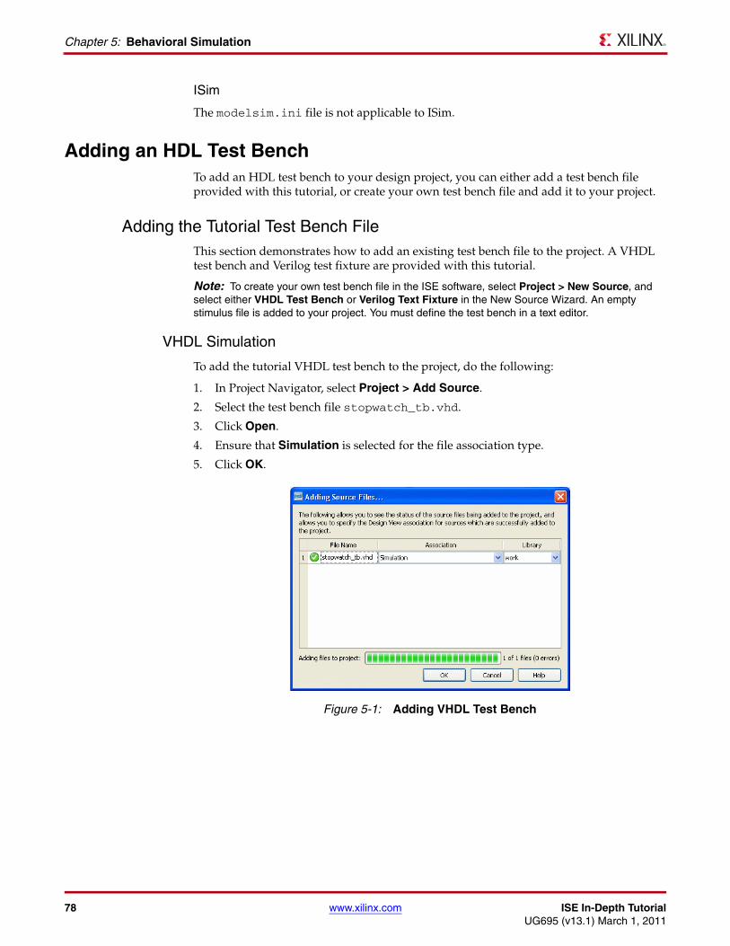
78 www.xilinx.com ISE In-Depth TutorialUG695 (v13.1) March 1, 2011
Chapter 5: Behavioral Simulation
ISim
The modelsim.ini file is not applicable to ISim.
Adding an HDL Test BenchTo add an HDL test bench to your design project, you can either add a test bench file provided with this tutorial, or create your own test bench file and add it to your project.
Adding the Tutorial Test Bench FileThis section demonstrates how to add an existing test bench file to the project. A VHDL test bench and Verilog test fixture are provided with this tutorial.
Note: To create your own test bench file in the ISE software, select Project > New Source, and select either VHDL Test Bench or Verilog Text Fixture in the New Source Wizard. An empty stimulus file is added to your project. You must define the test bench in a text editor.
VHDL Simulation
To add the tutorial VHDL test bench to the project, do the following:
1. In Project Navigator, select Project > Add Source.
2. Select the test bench file stopwatch_tb.vhd.
3. Click Open.
4. Ensure that Simulation is selected for the file association type.
5. Click OK.X-Ref Target - Figure 5-1
Figure 5-1: Adding VHDL Test Bench
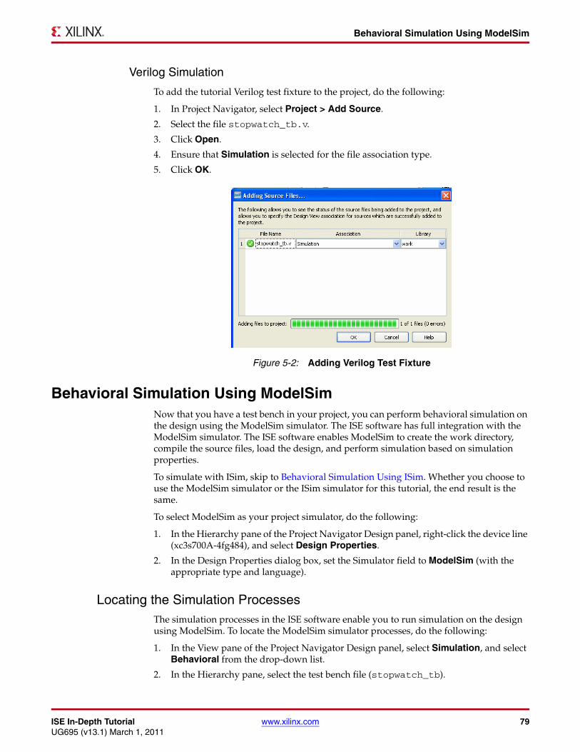
ISE In-Depth Tutorial www.xilinx.com 79UG695 (v13.1) March 1, 2011
Behavioral Simulation Using ModelSim
Verilog Simulation
To add the tutorial Verilog test fixture to the project, do the following:
1. In Project Navigator, select Project > Add Source.
2. Select the file stopwatch_tb.v.
3. Click Open.
4. Ensure that Simulation is selected for the file association type.
5. Click OK.
Behavioral Simulation Using ModelSimNow that you have a test bench in your project, you can perform behavioral simulation on the design using the ModelSim simulator. The ISE software has full integration with the ModelSim simulator. The ISE software enables ModelSim to create the work directory, compile the source files, load the design, and perform simulation based on simulation properties.
To simulate with ISim, skip to Behavioral Simulation Using ISim. Whether you choose to use the ModelSim simulator or the ISim simulator for this tutorial, the end result is the same.
To select ModelSim as your project simulator, do the following:
1. In the Hierarchy pane of the Project Navigator Design panel, right-click the device line (xc3s700A-4fg484), and select Design Properties.
2. In the Design Properties dialog box, set the Simulator field to ModelSim (with the appropriate type and language).
Locating the Simulation ProcessesThe simulation processes in the ISE software enable you to run simulation on the design using ModelSim. To locate the ModelSim simulator processes, do the following:
1. In the View pane of the Project Navigator Design panel, select Simulation, and select Behavioral from the drop-down list.
2. In the Hierarchy pane, select the test bench file (stopwatch_tb).
X-Ref Target - Figure 5-2
Figure 5-2: Adding Verilog Test Fixture
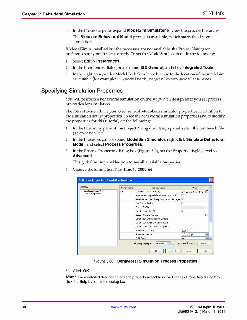
80 www.xilinx.com ISE In-Depth TutorialUG695 (v13.1) March 1, 2011
Chapter 5: Behavioral Simulation
3. In the Processes pane, expand ModelSim Simulator to view the process hierarchy.
The Simulate Behavioral Model process is available, which starts the design simulation.
If ModelSim is installed but the processes are not available, the Project Navigator preferences may not be set correctly. To set the ModelSim location, do the following:
1. Select Edit > Preferences.
2. In the Preferences dialog box, expand ISE General, and click Integrated Tools.
3. In the right pane, under Model Tech Simulator, browse to the location of the modelsim executable (for example: C:\modeltech_xe\win32xoem\modelsim.exe).
Specifying Simulation PropertiesYou will perform a behavioral simulation on the stopwatch design after you set process properties for simulation.
The ISE software allows you to set several ModelSim simulator properties in addition to the simulation netlist properties. To see the behavioral simulation properties and to modify the properties for this tutorial, do the following:
1. In the Hierarchy pane of the Project Navigator Design panel, select the test bench file (stopwatch_tb).
2. In the Processes pane, expand ModelSim Simulator, right-click Simulate Behavioral Model, and select Process Properties.
3. In the Process Properties dialog box (Figure 5-3), set the Property display level to Advanced.
This global setting enables you to see all available properties.
4. Change the Simulation Run Time to 2000 ns.
5. Click OK.
Note: For a detailed description of each property available in the Process Properties dialog box, click the Help button in the dialog box.
X-Ref Target - Figure 5-3
Figure 5-3: Behavioral Simulation Process Properties
ISE In-Depth Tutorial www.xilinx.com 81UG695 (v13.1) March 1, 2011
Behavioral Simulation Using ModelSim
Performing SimulationAfter the process properties have been set, you are ready to run ModelSim. To start the behavioral simulation, double-click Simulate Behavioral Model. ModelSim creates the work directory, compiles the source files, loads the design, and performs simulation for the time specified.
The majority of this design runs at 100 Hz and would take a significant amount of time to simulate. The first outputs to transition after RESET is released are the SF_D and LCD_E control signals, at around 33 ms. This is why the counter may seem like it is not working in a short simulation. For the purpose of this tutorial, only the DCM signals are monitored to verify that they work correctly.
Adding SignalsTo view internal signals during the simulation, you must add them to the Wave window. The ISE software automatically adds all the top-level ports to the Wave window. Additional signals are displayed in the Signal window based on the selected structure in the Structure window.
There are two basic methods for adding signals to the Simulator Wave window:
• Drag and drop from the Signal/Object window.
• Highlight signals in the Signal/Object window, and select Add > Wave > Selected Signals.
The following procedure explains how to add additional signals in the design hierarchy. In this tutorial, you will be adding the DCM signals to the waveform.
If you are using ModelSim version 6.0 or higher, all the windows are docked by default. To undock the windows, click the Undock icon.
To add additional signals in the design hierarchy, do the following:
1. In the Structure/Instance window, expand the uut hierarchy.
X-Ref Target - Figure 5-4
Figure 5-4: Undock Icon
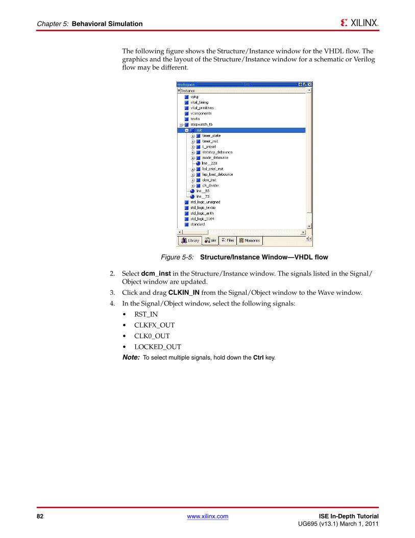
82 www.xilinx.com ISE In-Depth TutorialUG695 (v13.1) March 1, 2011
Chapter 5: Behavioral Simulation
The following figure shows the Structure/Instance window for the VHDL flow. The graphics and the layout of the Structure/Instance window for a schematic or Verilog flow may be different.
2. Select dcm_inst in the Structure/Instance window. The signals listed in the Signal/Object window are updated.
3. Click and drag CLKIN_IN from the Signal/Object window to the Wave window.
4. In the Signal/Object window, select the following signals:
• RST_IN
• CLKFX_OUT
• CLK0_OUT
• LOCKED_OUT
Note: To select multiple signals, hold down the Ctrl key.
X-Ref Target - Figure 5-5
Figure 5-5: Structure/Instance Window—VHDL flow
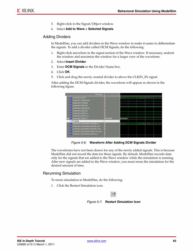
ISE In-Depth Tutorial www.xilinx.com 83UG695 (v13.1) March 1, 2011
Behavioral Simulation Using ModelSim
5. Right-click in the Signal/Object window.
6. Select Add to Wave > Selected Signals.
Adding Dividers
In ModelSim, you can add dividers in the Wave window to make it easier to differentiate the signals. To add a divider called DCM Signals, do the following:
1. Right-click anywhere in the signal section of the Wave window. If necessary, undock the window and maximize the window for a larger view of the waveform.
2. Select Insert Divider.
3. Enter DCM Signals in the Divider Name box.
4. Click OK.
5. Click and drag the newly created divider to above the CLKIN_IN signal.
After adding the DCM Signals divider, the waveform will appear as shown in the following figure.
The waveforms have not been drawn for any of the newly added signals. This is because ModelSim did not record the data for these signals. By default, ModelSim records data only for the signals that are added to the Wave window while the simulation is running. After new signals are added to the Wave window, you must rerun the simulation for the desired amount of time.
Rerunning Simulation
To rerun simulation in ModelSim, do the following:
1. Click the Restart Simulation icon.
X-Ref Target - Figure 5-6
Figure 5-6: Waveform After Adding DCM Signals Divider
X-Ref Target - Figure 5-7
Figure 5-7: Restart Simulation Icon
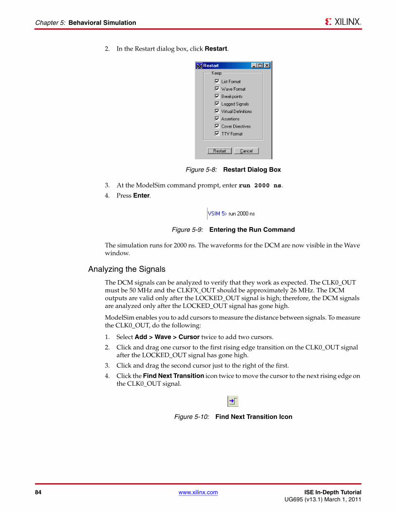
84 www.xilinx.com ISE In-Depth TutorialUG695 (v13.1) March 1, 2011
Chapter 5: Behavioral Simulation
2. In the Restart dialog box, click Restart.
3. At the ModelSim command prompt, enter run 2000 ns.
4. Press Enter.
The simulation runs for 2000 ns. The waveforms for the DCM are now visible in the Wave window.
Analyzing the Signals
The DCM signals can be analyzed to verify that they work as expected. The CLK0_OUT must be 50 MHz and the CLKFX_OUT should be approximately 26 MHz. The DCM outputs are valid only after the LOCKED_OUT signal is high; therefore, the DCM signals are analyzed only after the LOCKED_OUT signal has gone high.
ModelSim enables you to add cursors to measure the distance between signals. To measure the CLK0_OUT, do the following:
1. Select Add > Wave > Cursor twice to add two cursors.
2. Click and drag one cursor to the first rising edge transition on the CLK0_OUT signal after the LOCKED_OUT signal has gone high.
3. Click and drag the second cursor just to the right of the first.
4. Click the Find Next Transition icon twice to move the cursor to the next rising edge on the CLK0_OUT signal.
X-Ref Target - Figure 5-8
Figure 5-8: Restart Dialog Box
X-Ref Target - Figure 5-9
Figure 5-9: Entering the Run Command
X-Ref Target - Figure 5-10
Figure 5-10: Find Next Transition Icon
ISE In-Depth Tutorial www.xilinx.com 85UG695 (v13.1) March 1, 2011
Behavioral Simulation Using ISim
5. Look at the bottom of the waveform for the distance between the two cursors.
The measurement should read 20000 ps. This converts to 50 MHz, which is the input frequency from the test bench, which in turn should be the DCM CLK0 output.
6. Measure CLKFX_OUT using the same steps as above. The measurement should read 38462 ps. This comes out to approximately 26 MHz.
Saving the SimulationThe ModelSim simulator enables you to save the signals list in the Wave window after new signals or stimuli are added, and after simulation is rerun. The saved signals list can easily be opened each time the simulation is started.
To save the signals list, do the following:
1. In the Wave window, select File > Save as.
2. In the Save Format dialog box, rename the file name from the default wave.do to dcm_signal.do.
3. Click Save.
After restarting the simulation, select File > Load in the Wave window to load this file.
Your behavioral simulation is complete. To implement the design, follow the steps in Chapter 6, Design Implementation.
Behavioral Simulation Using ISimFollow this section of the tutorial if you have skipped the previous section, Behavioral Simulation Using ModelSim.
Now that you have a test bench in your project, you can perform behavioral simulation on the design using ISim. The ISE software has full integration with ISim. The ISE software enables ISim to create the work directory, compile the source files, load the design, and perform simulation based on simulation properties.
To select ISim as your project simulator, do the following:
1. In the Hierarchy pane of the Project Navigator Design panel, right-click the device line (xc3s700A-4fg484), and select Design Properties.
2. In the Design Properties dialog box, set the Simulator field to ISim (VHDL/Verilog).
Locating the Simulation ProcessesThe simulation processes in the ISE software enable you to run simulation on the design using ISim. To locate the ISim processes, do the following:
1. In the View pane of the Project Navigator Design panel, select Simulation, and select Behavioral from the drop-down list.
2. In the Hierarchy pane, select the test bench file (stopwatch_tb).
3. In the Processes pane, expand ISim Simulator to view the process hierarchy.
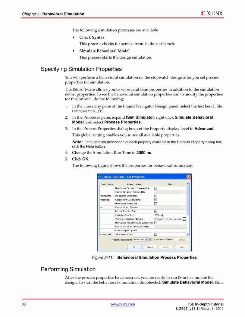
86 www.xilinx.com ISE In-Depth TutorialUG695 (v13.1) March 1, 2011
Chapter 5: Behavioral Simulation
The following simulation processes are available:
• Check Syntax
This process checks for syntax errors in the test bench.
• Simulate Behavioral Model
This process starts the design simulation.
Specifying Simulation PropertiesYou will perform a behavioral simulation on the stopwatch design after you set process properties for simulation.
The ISE software allows you to set several ISim properties in addition to the simulation netlist properties. To see the behavioral simulation properties and to modify the properties for this tutorial, do the following:
1. In the Hierarchy pane of the Project Navigator Design panel, select the test bench file (stopwatch_tb).
2. In the Processes pane, expand ISim Simulator, right-click Simulate Behavioral Model, and select Process Properties.
3. In the Process Properties dialog box, set the Property display level to Advanced.
This global setting enables you to see all available properties.
Note: For a detailed description of each property available in the Process Property dialog box, click the Help button.
4. Change the Simulation Run Time to 2000 ns.
5. Click OK.
The following figure shows the properties for behavioral simulation.
Performing SimulationAfter the process properties have been set, you are ready to run ISim to simulate the design. To start the behavioral simulation, double-click Simulate Behavioral Model. ISim
X-Ref Target - Figure 5-11
Figure 5-11: Behavioral Simulation Process Properties
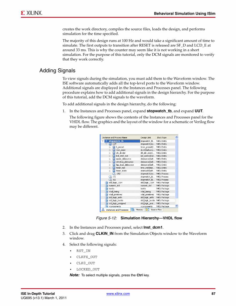
ISE In-Depth Tutorial www.xilinx.com 87UG695 (v13.1) March 1, 2011
Behavioral Simulation Using ISim
creates the work directory, compiles the source files, loads the design, and performs simulation for the time specified.
The majority of this design runs at 100 Hz and would take a significant amount of time to simulate. The first outputs to transition after RESET is released are SF_D and LCD_E at around 33 ms. This is why the counter may seem like it is not working in a short simulation. For the purpose of this tutorial, only the DCM signals are monitored to verify that they work correctly.
Adding SignalsTo view signals during the simulation, you must add them to the Waveform window. The ISE software automatically adds all the top-level ports to the Waveform window. Additional signals are displayed in the Instances and Processes panel. The following procedure explains how to add additional signals in the design hierarchy. For the purpose of this tutorial, add the DCM signals to the waveform.
To add additional signals in the design hierarchy, do the following:
1. In the Instances and Processes panel, expand stopwatch_tb, and expand UUT.
The following figure shows the contents of the Instances and Processes panel for the VHDL flow. The graphics and the layout of the window for a schematic or Verilog flow may be different.
2. In the Instances and Processes panel, select Inst_dcm1.
3. Click and drag CLKIN_IN from the Simulation Objects window to the Waveform window.
4. Select the following signals:
• RST_IN
• CLKFX_OUT
• CLK0_OUT
• LOCKED_OUT
Note: To select multiple signals, press the Ctrl key.
X-Ref Target - Figure 5-12
Figure 5-12: Simulation Hierarchy—VHDL flow
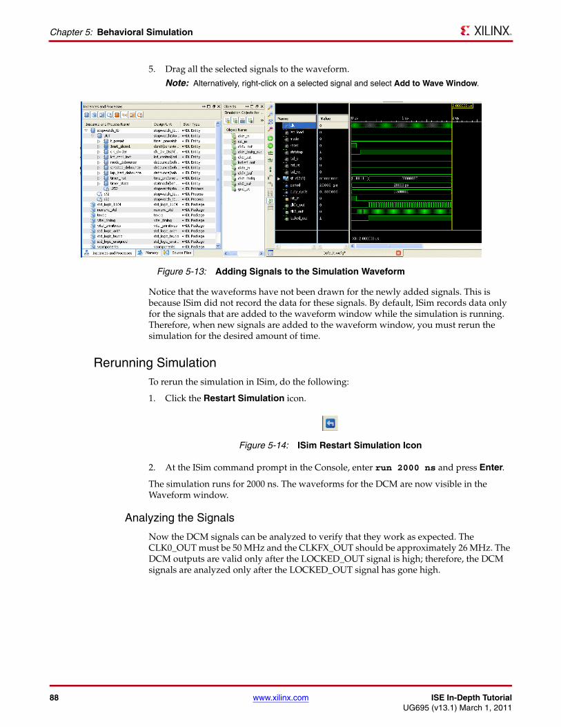
88 www.xilinx.com ISE In-Depth TutorialUG695 (v13.1) March 1, 2011
Chapter 5: Behavioral Simulation
5. Drag all the selected signals to the waveform.
Note: Alternatively, right-click on a selected signal and select Add to Wave Window.
Notice that the waveforms have not been drawn for the newly added signals. This is because ISim did not record the data for these signals. By default, ISim records data only for the signals that are added to the waveform window while the simulation is running. Therefore, when new signals are added to the waveform window, you must rerun the simulation for the desired amount of time.
Rerunning SimulationTo rerun the simulation in ISim, do the following:
1. Click the Restart Simulation icon.
2. At the ISim command prompt in the Console, enter run 2000 ns and press Enter.
The simulation runs for 2000 ns. The waveforms for the DCM are now visible in the Waveform window.
Analyzing the Signals
Now the DCM signals can be analyzed to verify that they work as expected. The CLK0_OUT must be 50 MHz and the CLKFX_OUT should be approximately 26 MHz. The DCM outputs are valid only after the LOCKED_OUT signal is high; therefore, the DCM signals are analyzed only after the LOCKED_OUT signal has gone high.
X-Ref Target - Figure 5-13
Figure 5-13: Adding Signals to the Simulation Waveform
X-Ref Target - Figure 5-14
Figure 5-14: ISim Restart Simulation Icon
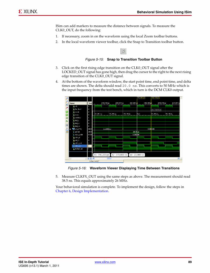
ISE In-Depth Tutorial www.xilinx.com 89UG695 (v13.1) March 1, 2011
Behavioral Simulation Using ISim
ISim can add markers to measure the distance between signals. To measure the CLK0_OUT, do the following:
1. If necessary, zoom in on the waveform using the local Zoom toolbar buttons.
2. In the local waveform viewer toolbar, click the Snap to Transition toolbar button.
3. Click on the first rising edge transition on the CLK0_OUT signal after the LOCKED_OUT signal has gone high, then drag the cursor to the right to the next rising edge transition of the CLK0_OUT signal.
4. At the bottom of the waveform window, the start point time, end point time, and delta times are shown. The delta should read 20.0 ns. This converts to 50 MHz which is the input frequency from the test bench, which in turn is the DCM CLK0 output.
5. Measure CLKFX_OUT using the same steps as above. The measurement should read 38.5 ns. This equals approximately 26 MHz.
Your behavioral simulation is complete. To implement the design, follow the steps in Chapter 6, Design Implementation.
X-Ref Target - Figure 5-15
Figure 5-15: Snap to Transition Toolbar Button
X-Ref Target - Figure 5-16
Figure 5-16: Waveform Viewer Displaying Time Between Transitions

90 www.xilinx.com ISE In-Depth TutorialUG695 (v13.1) March 1, 2011
Chapter 5: Behavioral Simulation
ISE In-Depth Tutorial www.xilinx.com 91UG695 (v13.1) March 1, 2011
Chapter 6
Design Implementation
Overview of Design ImplementationDesign implementation is the process of translating, mapping, placing, routing, and generating a bitstream file for your design. The design implementation tools are embedded in the Xilinx® ISE® software for easy access and project management.
This chapter is the first in the Implementation-Only Flow and is a subsequent chapter for the HDL Design Flow and the Schematic Design Flow.
This chapter demonstrates the ISE software implementation flow. The front-end design has already been compiled in an EDA interface tool. For details about compiling the design, see Chapter 3, HDL-Based Design or Chapter 4, Schematic-Based Design. In this chapter, you will be passing a synthesized netlist (EDN, NGC) from the front-end tool to the back-end design implementation tools, and you will be incorporating placement constraints through a User Constraints File (UCF). You will also add timing constraints as well as additional placement constraints.
Getting StartedThe tutorial design emulates a runner’s stopwatch with actual and lap times. There are five inputs to the system: CLK, RESET, LAP_LOAD, MODE, and SRTSTP. This system generates a traditional stopwatch with lap times and a traditional timer on an LCD display.
Continuing from Design EntryIf you have followed the tutorial using either the HDL design flow or the schematic design flow, you have created a project, completed source files, and synthesized the design.
If you do not have a stopwatch.ucf constraint file in your project, create one as follows:
1. In the Hierarchy pane of the Project Navigator Design panel, select the top-level source file stopwatch.
2. Select Project > New Source.
3. Select Implementation Constraints File.
4. Enter stopwatch.ucf as the file name.
5. Click Next.
6. Click Finish.
With a UCF in the project, you are now ready to begin this chapter. Skip to the Specifying Options section.
92 www.xilinx.com ISE In-Depth TutorialUG695 (v13.1) March 1, 2011
Chapter 6: Design Implementation
Starting from Design ImplementationIf you are beginning the tutorial from this chapter, you will need to download the pre-synthesized design files provided on the Xilinx website, create a project in the ISE software, and then add the downloaded source files to the project.
1. Create an empty working directory named Watch.
2. Copy the pre-synthesized tutorial files shown in the following table to your newly created working directory. The files are provided with the ISE Design Suite Tutorials available from the Xilinx website.
3. Open the ISE software using one of the following methods:
a. On a workstation, enter ise.
b. On a PC, select Start > Programs > Xilinx ISE Design Suite > ISE Design Tools > Project Navigator.
4. Create a new project, and add the EDIF netlist as follows:
a. Select File > New Project.
b. In the Name field, enter wtut_edif.
c. Select EDIF for the Top-Level Source Type, and click Next.
d. Select stopwatch.edf or stopwatch.edn for the Input Design file.
e. Select stopwatch.ucf for the Constraints file, and click Next.
f. Select the following values:
- Family: Spartan3A and Spartan3AN
- Device: XC3S700A
- Package: FG484
- Speed: -4
g. Click Next., then Finish to complete the project creation.
Note: If the timer_preset.ngc file is not in the project directory, copy it from the extracted ZIP file.
Table 6-1: Required Tutorial Files
File Name Description
stopwatch.edn, stopwatch.edf or stopwatch.ngc
Input netlist file (EDIF)
timer_preset.ngc Timer netlist file (NGC)
stopwatch.ucf User Constraints File
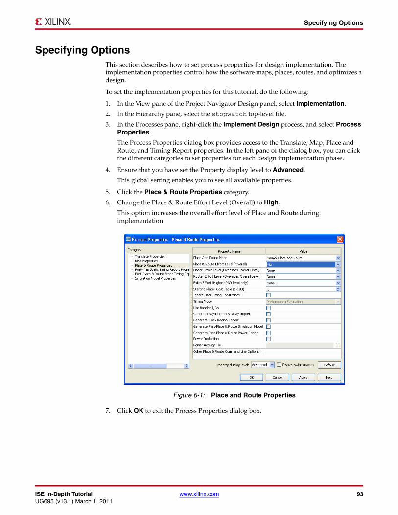
ISE In-Depth Tutorial www.xilinx.com 93UG695 (v13.1) March 1, 2011
Specifying Options
Specifying OptionsThis section describes how to set process properties for design implementation. The implementation properties control how the software maps, places, routes, and optimizes a design.
To set the implementation properties for this tutorial, do the following:
1. In the View pane of the Project Navigator Design panel, select Implementation.
2. In the Hierarchy pane, select the stopwatch top-level file.
3. In the Processes pane, right-click the Implement Design process, and select Process Properties.
The Process Properties dialog box provides access to the Translate, Map, Place and Route, and Timing Report properties. In the left pane of the dialog box, you can click the different categories to set properties for each design implementation phase.
4. Ensure that you have set the Property display level to Advanced.
This global setting enables you to see all available properties.
5. Click the Place & Route Properties category.
6. Change the Place & Route Effort Level (Overall) to High.
This option increases the overall effort level of Place and Route during implementation.
7. Click OK to exit the Process Properties dialog box.
X-Ref Target - Figure 6-1
Figure 6-1: Place and Route Properties
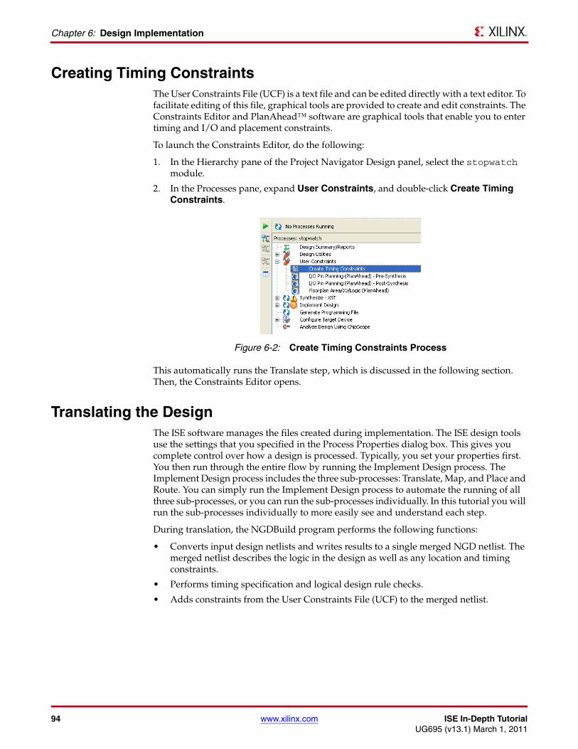
94 www.xilinx.com ISE In-Depth TutorialUG695 (v13.1) March 1, 2011
Chapter 6: Design Implementation
Creating Timing ConstraintsThe User Constraints File (UCF) is a text file and can be edited directly with a text editor. To facilitate editing of this file, graphical tools are provided to create and edit constraints. The Constraints Editor and PlanAhead™ software are graphical tools that enable you to enter timing and I/O and placement constraints.
To launch the Constraints Editor, do the following:
1. In the Hierarchy pane of the Project Navigator Design panel, select the stopwatch module.
2. In the Processes pane, expand User Constraints, and double-click Create Timing Constraints.
This automatically runs the Translate step, which is discussed in the following section. Then, the Constraints Editor opens.
Translating the DesignThe ISE software manages the files created during implementation. The ISE design tools use the settings that you specified in the Process Properties dialog box. This gives you complete control over how a design is processed. Typically, you set your properties first. You then run through the entire flow by running the Implement Design process. The Implement Design process includes the three sub-processes: Translate, Map, and Place and Route. You can simply run the Implement Design process to automate the running of all three sub-processes, or you can run the sub-processes individually. In this tutorial you will run the sub-processes individually to more easily see and understand each step.
During translation, the NGDBuild program performs the following functions:
• Converts input design netlists and writes results to a single merged NGD netlist. The merged netlist describes the logic in the design as well as any location and timing constraints.
• Performs timing specification and logical design rule checks.
• Adds constraints from the User Constraints File (UCF) to the merged netlist.
X-Ref Target - Figure 6-2
Figure 6-2: Create Timing Constraints Process
ISE In-Depth Tutorial www.xilinx.com 95UG695 (v13.1) March 1, 2011
Using the Constraints Editor
Using the Constraints EditorWhen you run the Create Timing Constraints process, Translate is automatically run and the ISE software launches the Constraints Editor.
The Constraints Editor enables you to do the following:
• Edit constraints previously defined in a UCF file.
• Add new constraints to your design.
Following are input files to the Constraints Editor:
• NGD (Native Generic Database) File
The NGD file serves as input to the mapper, which then outputs the physical design database, an NCD (Native Circuit Description) file.
• Corresponding UCF (User Constraint File)
All UCF files that are part of the ISE project are passed to Constraints Editor.
Multiple UCF files are supported in ISE projects. All constraint files in the project are read by the Constraints Editor, and constraints that you edit are updated in the originating constraint file. New constraints are written to the UCF file specified in Constraints Editor.
The Translate step (NGDBuild) uses the UCF file, along with design source netlists, to produce a newer NGD file, which incorporates the changes made. The Map program (the next section in the design flow) then reads the NGD. In this design, the stopwatch.ngd and stopwatch.ucf files are automatically read into the Constraints Editor.
In the following section, a PERIOD, Global OFFSET IN, Global OFFSET OUT, and TIMEGRP OFFSET IN constraint will be created and written in the UCF and used during implementation. The Clock Domains branch of the Timing Constraints tab automatically displays all the clock nets in your design, and enables you to define the associated period, pad to setup, and clock to pad values. Note that many of the internal names will vary depending on the design flow and synthesis tool used.
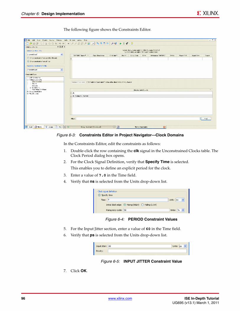
96 www.xilinx.com ISE In-Depth TutorialUG695 (v13.1) March 1, 2011
Chapter 6: Design Implementation
The following figure shows the Constraints Editor.
In the Constraints Editor, edit the constraints as follows:
1. Double-click the row containing the clk signal in the Unconstrained Clocks table. The Clock Period dialog box opens.
2. For the Clock Signal Definition, verify that Specify Time is selected.
This enables you to define an explicit period for the clock.
3. Enter a value of 7.0 in the Time field.
4. Verify that ns is selected from the Units drop-down list.
5. For the Input Jitter section, enter a value of 60 in the Time field.
6. Verify that ps is selected from the Units drop-down list.
7. Click OK.
X-Ref Target - Figure 6-3
Figure 6-3: Constraints Editor in Project Navigator—Clock Domains
X-Ref Target - Figure 6-4
Figure 6-4: PERIOD Constraint Values
X-Ref Target - Figure 6-5
Figure 6-5: INPUT JITTER Constraint Value
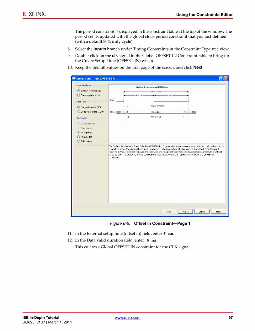
ISE In-Depth Tutorial www.xilinx.com 97UG695 (v13.1) March 1, 2011
Using the Constraints Editor
The period constraint is displayed in the constraint table at the top of the window. The period cell is updated with the global clock period constraint that you just defined (with a default 50% duty cycle).
8. Select the Inputs branch under Timing Constraints in the Constraint Type tree view.
9. Double-click on the clk signal in the Global OFFSET IN Constraint table to bring up the Create Setup Time (OFFSET IN) wizard.
10. Keep the default values on the first page of the screen, and click Next.
11. In the External setup time (offset in) field, enter 6 ns.
12. In the Data valid duration field, enter 6 ns.
This creates a Global OFFSET IN constraint for the CLK signal.
X-Ref Target - Figure 6-6
Figure 6-6: Offset In Constraint—Page 1
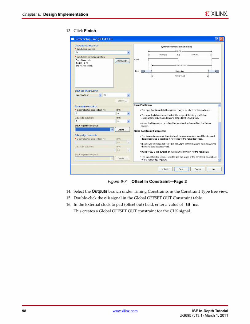
98 www.xilinx.com ISE In-Depth TutorialUG695 (v13.1) March 1, 2011
Chapter 6: Design Implementation
13. Click Finish.
14. Select the Outputs branch under Timing Constraints in the Constraint Type tree view.
15. Double-click the clk signal in the Global OFFSET OUT Constraint table.
16. In the External clock to pad (offset out) field, enter a value of 38 ns.
This creates a Global OFFSET OUT constraint for the CLK signal.
X-Ref Target - Figure 6-7
Figure 6-7: Offset In Constraint—Page 2
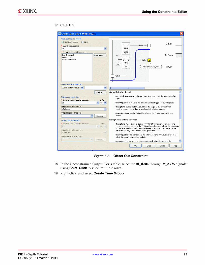
ISE In-Depth Tutorial www.xilinx.com 99UG695 (v13.1) March 1, 2011
Using the Constraints Editor
17. Click OK.
18. In the Unconstrained Output Ports table, select the sf_d<0> through sf_d<7> signals using Shift+Click to select multiple rows.
19. Right-click, and select Create Time Group.
X-Ref Target - Figure 6-8
Figure 6-8: Offset Out Constraint
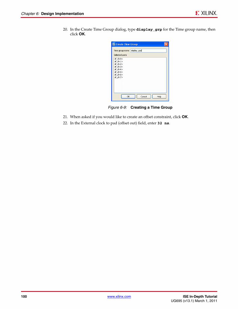
100 www.xilinx.com ISE In-Depth TutorialUG695 (v13.1) March 1, 2011
Chapter 6: Design Implementation
20. In the Create Time Group dialog, type display_grp for the Time group name, then click OK.
21. When asked if you would like to create an offset constraint, click OK.
22. In the External clock to pad (offset out) field, enter 32 ns.
X-Ref Target - Figure 6-9
Figure 6-9: Creating a Time Group
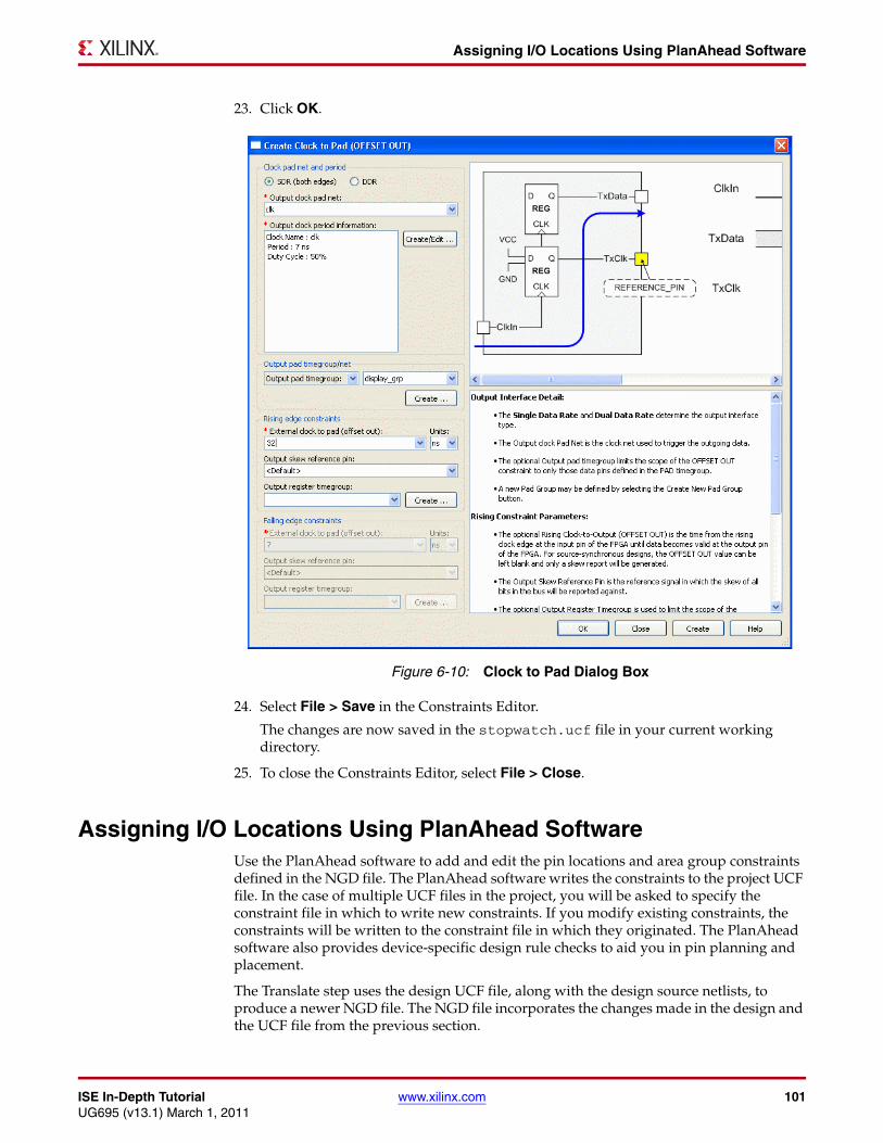
ISE In-Depth Tutorial www.xilinx.com 101UG695 (v13.1) March 1, 2011
Assigning I/O Locations Using PlanAhead Software
23. Click OK.
24. Select File > Save in the Constraints Editor.
The changes are now saved in the stopwatch.ucf file in your current working directory.
25. To close the Constraints Editor, select File > Close.
Assigning I/O Locations Using PlanAhead SoftwareUse the PlanAhead software to add and edit the pin locations and area group constraints defined in the NGD file. The PlanAhead software writes the constraints to the project UCF file. In the case of multiple UCF files in the project, you will be asked to specify the constraint file in which to write new constraints. If you modify existing constraints, the constraints will be written to the constraint file in which they originated. The PlanAhead software also provides device-specific design rule checks to aid you in pin planning and placement.
The Translate step uses the design UCF file, along with the design source netlists, to produce a newer NGD file. The NGD file incorporates the changes made in the design and the UCF file from the previous section.
X-Ref Target - Figure 6-10
Figure 6-10: Clock to Pad Dialog Box
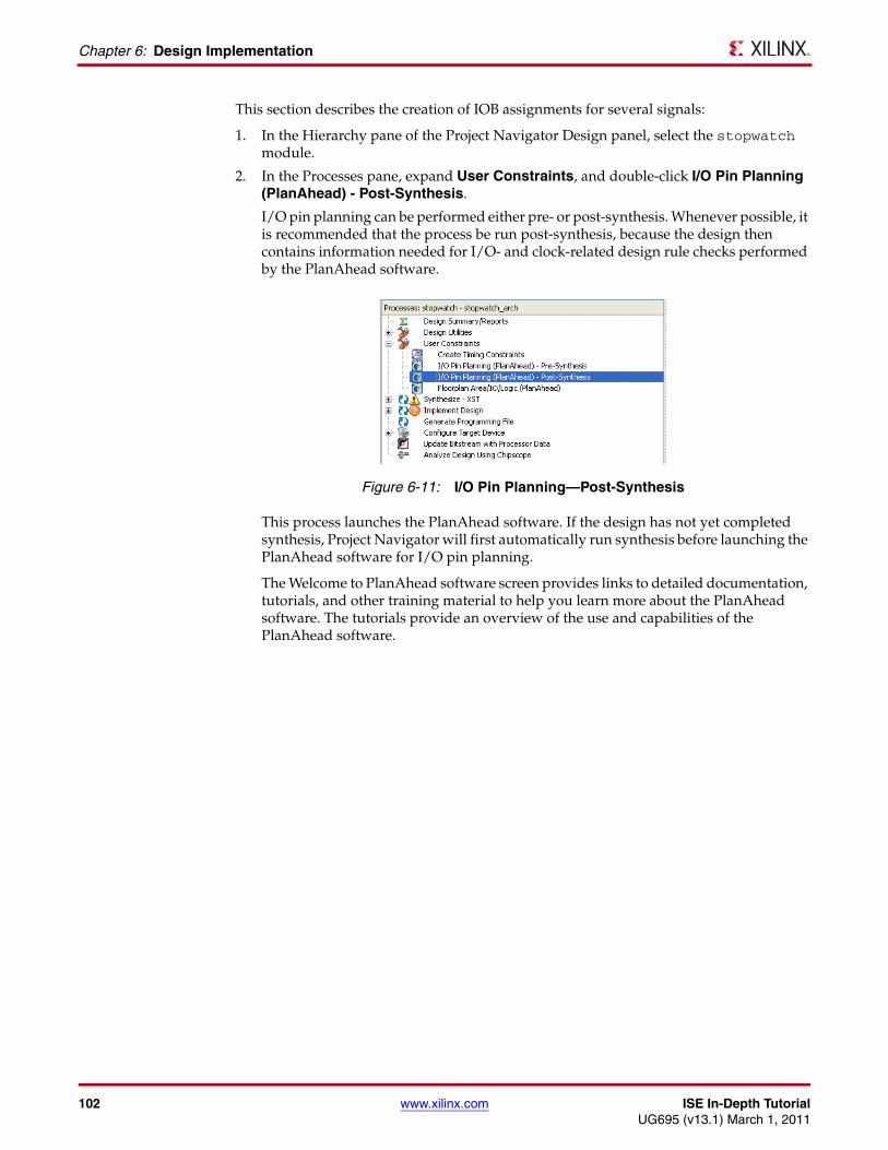
102 www.xilinx.com ISE In-Depth TutorialUG695 (v13.1) March 1, 2011
Chapter 6: Design Implementation
This section describes the creation of IOB assignments for several signals:
1. In the Hierarchy pane of the Project Navigator Design panel, select the stopwatch module.
2. In the Processes pane, expand User Constraints, and double-click I/O Pin Planning (PlanAhead) - Post-Synthesis.
I/O pin planning can be performed either pre- or post-synthesis. Whenever possible, it is recommended that the process be run post-synthesis, because the design then contains information needed for I/O- and clock-related design rule checks performed by the PlanAhead software.
This process launches the PlanAhead software. If the design has not yet completed synthesis, Project Navigator will first automatically run synthesis before launching the PlanAhead software for I/O pin planning.
The Welcome to PlanAhead software screen provides links to detailed documentation, tutorials, and other training material to help you learn more about the PlanAhead software. The tutorials provide an overview of the use and capabilities of the PlanAhead software.
X-Ref Target - Figure 6-11
Figure 6-11: I/O Pin Planning—Post-Synthesis
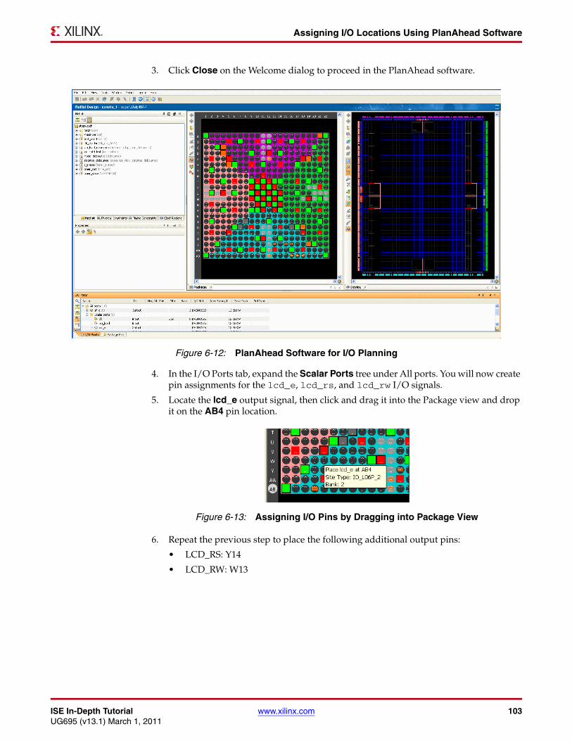
ISE In-Depth Tutorial www.xilinx.com 103UG695 (v13.1) March 1, 2011
Assigning I/O Locations Using PlanAhead Software
3. Click Close on the Welcome dialog to proceed in the PlanAhead software.
4. In the I/O Ports tab, expand the Scalar Ports tree under All ports. You will now create pin assignments for the lcd_e, lcd_rs, and lcd_rw I/O signals.
5. Locate the lcd_e output signal, then click and drag it into the Package view and drop it on the AB4 pin location.
6. Repeat the previous step to place the following additional output pins:
• LCD_RS: Y14
• LCD_RW: W13
X-Ref Target - Figure 6-12
Figure 6-12: PlanAhead Software for I/O Planning
X-Ref Target - Figure 6-13
Figure 6-13: Assigning I/O Pins by Dragging into Package View
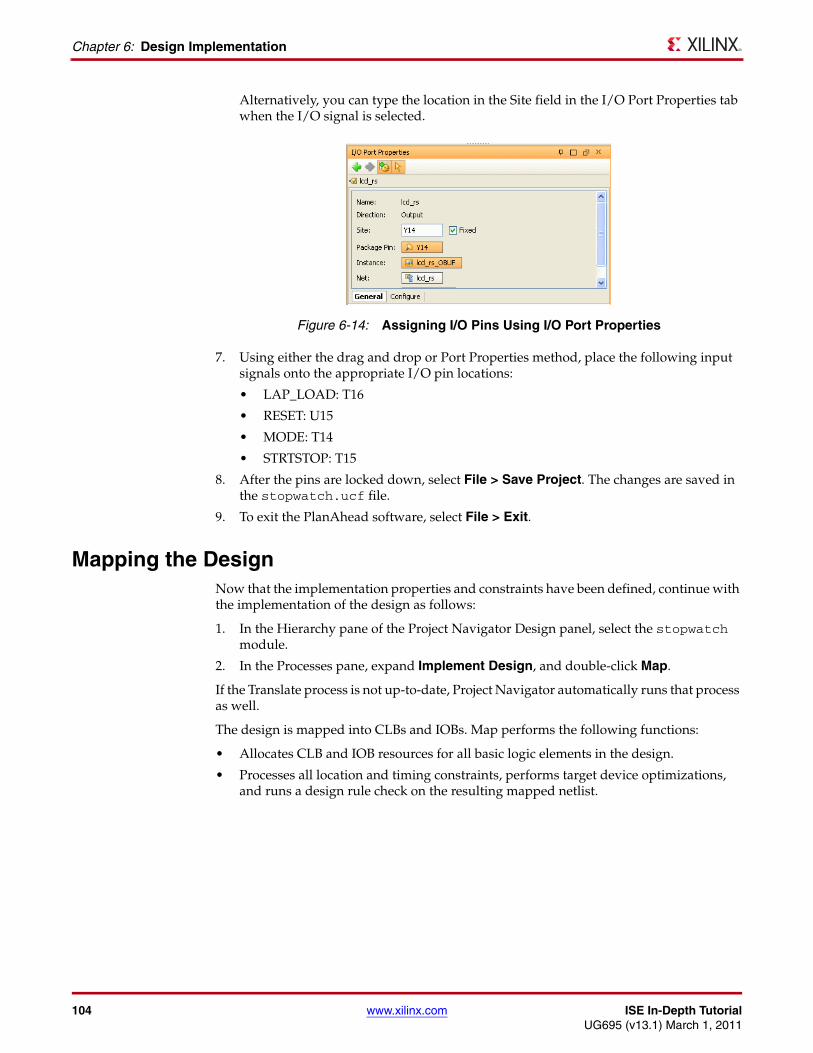
104 www.xilinx.com ISE In-Depth TutorialUG695 (v13.1) March 1, 2011
Chapter 6: Design Implementation
Alternatively, you can type the location in the Site field in the I/O Port Properties tab when the I/O signal is selected.
7. Using either the drag and drop or Port Properties method, place the following input signals onto the appropriate I/O pin locations:
• LAP_LOAD: T16
• RESET: U15
• MODE: T14
• STRTSTOP: T15
8. After the pins are locked down, select File > Save Project. The changes are saved in the stopwatch.ucf file.
9. To exit the PlanAhead software, select File > Exit.
Mapping the DesignNow that the implementation properties and constraints have been defined, continue with the implementation of the design as follows:
1. In the Hierarchy pane of the Project Navigator Design panel, select the stopwatch module.
2. In the Processes pane, expand Implement Design, and double-click Map.
If the Translate process is not up-to-date, Project Navigator automatically runs that process as well.
The design is mapped into CLBs and IOBs. Map performs the following functions:
• Allocates CLB and IOB resources for all basic logic elements in the design.
• Processes all location and timing constraints, performs target device optimizations, and runs a design rule check on the resulting mapped netlist.
X-Ref Target - Figure 6-14
Figure 6-14: Assigning I/O Pins Using I/O Port Properties
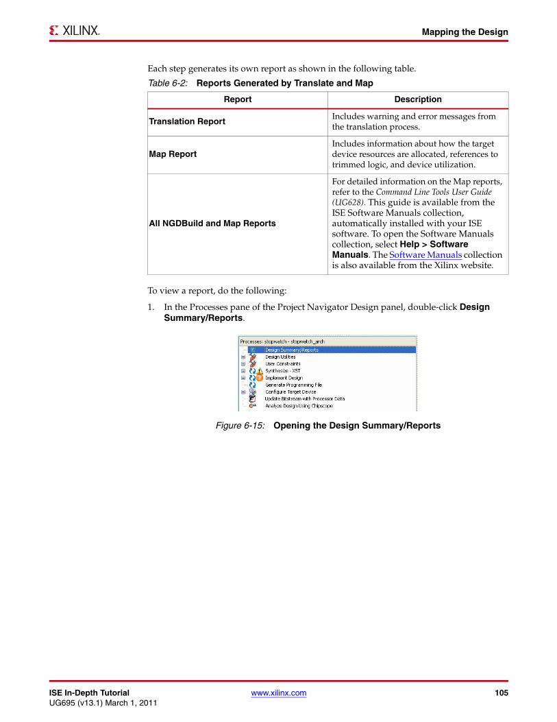
ISE In-Depth Tutorial www.xilinx.com 105UG695 (v13.1) March 1, 2011
Mapping the Design
Each step generates its own report as shown in the following table.
To view a report, do the following:
1. In the Processes pane of the Project Navigator Design panel, double-click Design Summary/Reports.
Table 6-2: Reports Generated by Translate and Map
Report Description
Translation ReportIncludes warning and error messages from the translation process.
Map ReportIncludes information about how the target device resources are allocated, references to trimmed logic, and device utilization.
All NGDBuild and Map Reports
For detailed information on the Map reports, refer to the Command Line Tools User Guide (UG628). This guide is available from the ISE Software Manuals collection, automatically installed with your ISE software. To open the Software Manuals collection, select Help > Software Manuals. The Software Manuals collection is also available from the Xilinx website.
X-Ref Target - Figure 6-15
Figure 6-15: Opening the Design Summary/Reports
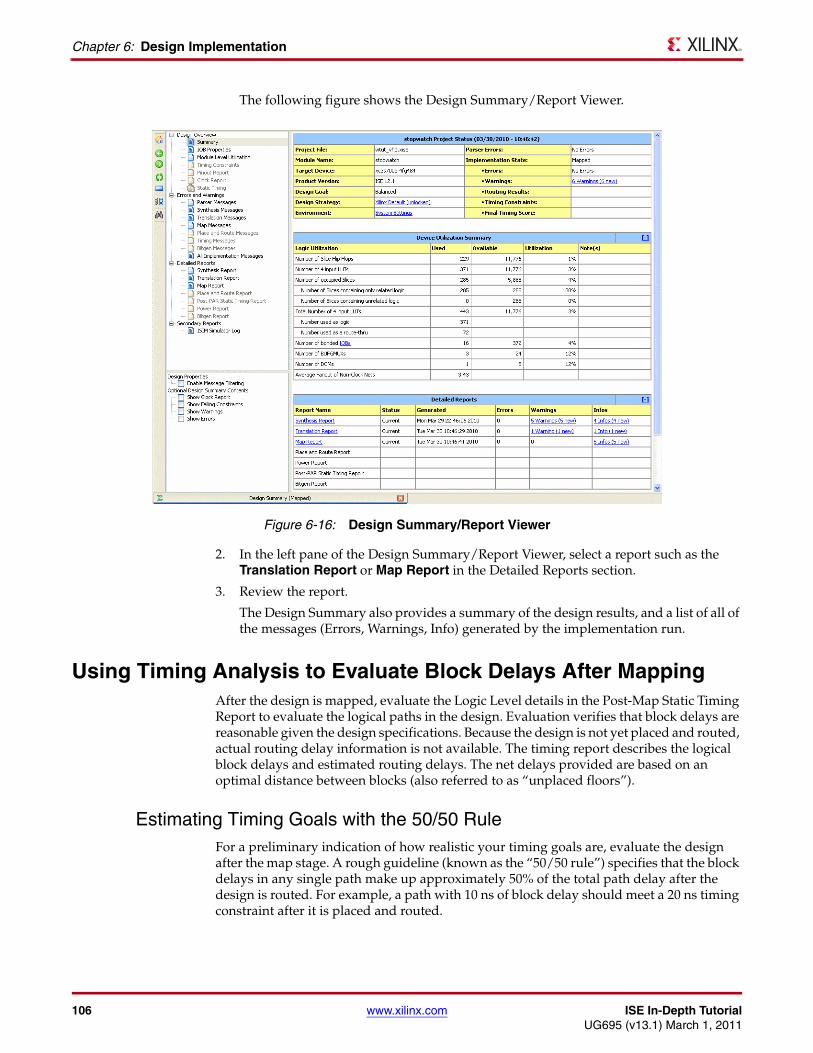
106 www.xilinx.com ISE In-Depth TutorialUG695 (v13.1) March 1, 2011
Chapter 6: Design Implementation
The following figure shows the Design Summary/Report Viewer.
2. In the left pane of the Design Summary/Report Viewer, select a report such as the Translation Report or Map Report in the Detailed Reports section.
3. Review the report.
The Design Summary also provides a summary of the design results, and a list of all of the messages (Errors, Warnings, Info) generated by the implementation run.
Using Timing Analysis to Evaluate Block Delays After MappingAfter the design is mapped, evaluate the Logic Level details in the Post-Map Static Timing Report to evaluate the logical paths in the design. Evaluation verifies that block delays are reasonable given the design specifications. Because the design is not yet placed and routed, actual routing delay information is not available. The timing report describes the logical block delays and estimated routing delays. The net delays provided are based on an optimal distance between blocks (also referred to as “unplaced floors”).
Estimating Timing Goals with the 50/50 RuleFor a preliminary indication of how realistic your timing goals are, evaluate the design after the map stage. A rough guideline (known as the “50/50 rule”) specifies that the block delays in any single path make up approximately 50% of the total path delay after the design is routed. For example, a path with 10 ns of block delay should meet a 20 ns timing constraint after it is placed and routed.
X-Ref Target - Figure 6-16
Figure 6-16: Design Summary/Report Viewer
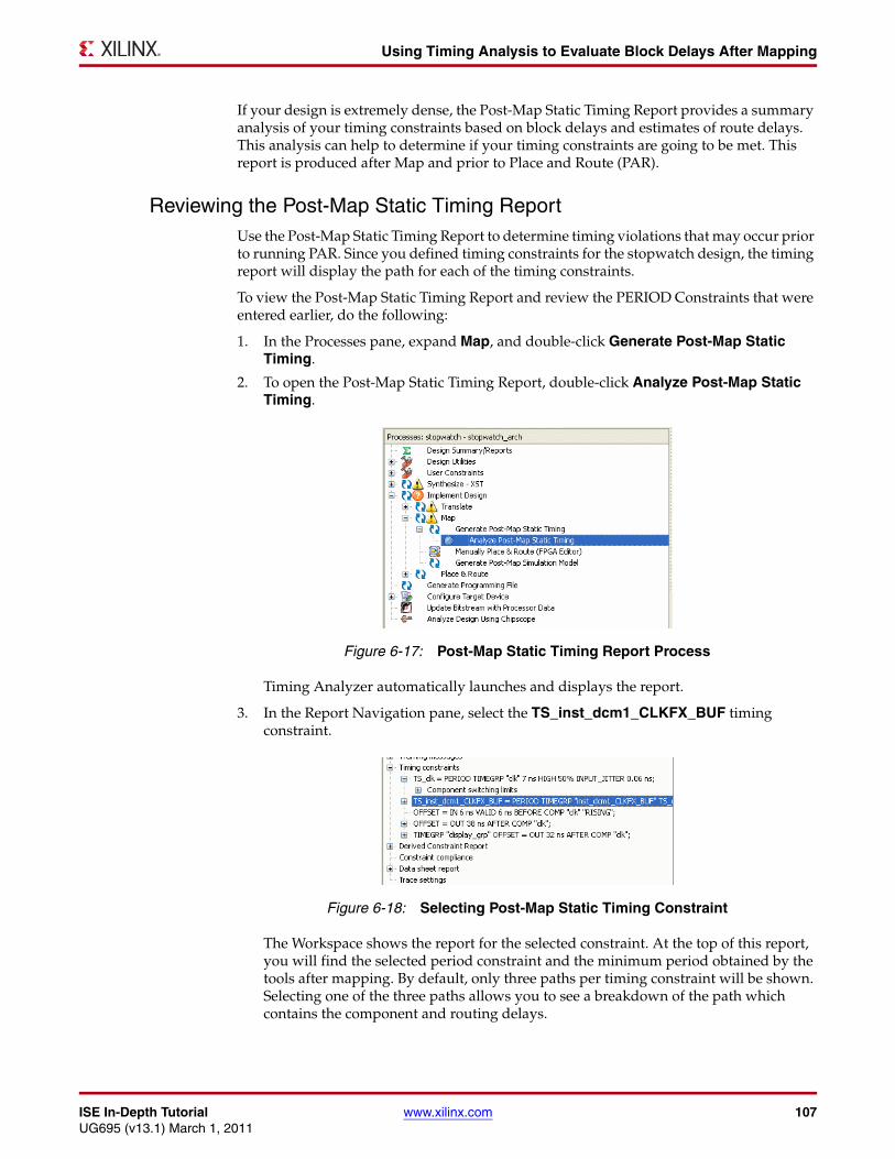
ISE In-Depth Tutorial www.xilinx.com 107UG695 (v13.1) March 1, 2011
Using Timing Analysis to Evaluate Block Delays After Mapping
If your design is extremely dense, the Post-Map Static Timing Report provides a summary analysis of your timing constraints based on block delays and estimates of route delays. This analysis can help to determine if your timing constraints are going to be met. This report is produced after Map and prior to Place and Route (PAR).
Reviewing the Post-Map Static Timing ReportUse the Post-Map Static Timing Report to determine timing violations that may occur prior to running PAR. Since you defined timing constraints for the stopwatch design, the timing report will display the path for each of the timing constraints.
To view the Post-Map Static Timing Report and review the PERIOD Constraints that were entered earlier, do the following:
1. In the Processes pane, expand Map, and double-click Generate Post-Map Static Timing.
2. To open the Post-Map Static Timing Report, double-click Analyze Post-Map Static Timing.
Timing Analyzer automatically launches and displays the report.
3. In the Report Navigation pane, select the TS_inst_dcm1_CLKFX_BUF timing constraint.
The Workspace shows the report for the selected constraint. At the top of this report, you will find the selected period constraint and the minimum period obtained by the tools after mapping. By default, only three paths per timing constraint will be shown. Selecting one of the three paths allows you to see a breakdown of the path which contains the component and routing delays.
X-Ref Target - Figure 6-17
Figure 6-17: Post-Map Static Timing Report Process
X-Ref Target - Figure 6-18
Figure 6-18: Selecting Post-Map Static Timing Constraint
108 www.xilinx.com ISE In-Depth TutorialUG695 (v13.1) March 1, 2011
Chapter 6: Design Implementation
Notice that the report displays the percentage of logic versus the percentage of routing at the end of each path (e.g. 88.0% logic, 12.0% route). The unplaced floors listed are estimates (indicated by the letter “e” next to the net delay) based on optimal placement of blocks.
4. After viewing the report, close the Timing Analyzer by selecting File > Close.
Note: Even if you do not generate a timing report, PAR still processes a design based on the relationship between the block delays, floors, and timing specifications for the design. For example, if a PERIOD constraint of 8 ns is specified for a path, and there are block delays of 7 ns and unplaced floor net delays of 3 ns, PAR stops and generates an error message. In this example, PAR fails because it determines that the total delay (10 ns) is greater than the constraint placed on the design (8 ns). The Post-Map Static Timing Report will list any pre-PAR timing violations.
Placing and Routing the DesignAfter the mapped design is evaluated, the design can be placed and routed. One of two place-and-route algorithms is performed during the Place and Route (PAR) process:
• Timing-Driven PAR
PAR is run with the timing constraints specified in the input netlist, the constraints file, or both.
• Non-Timing-Driven PAR
PAR is run, ignoring all timing constraints.
Because you defined timing constraints earlier in this chapter, the Place and Route (PAR) process performs timing-driven placement and routing.
To run Place and Route, do the following:
1. In the Hierarchy pane of the Project Navigator Design panel, select the stopwatch module.
2. In the Processes pane, expand Implement Design, and double-click Place & Route.
The Place and Route process generates the reports shown in the following table.
Note: Additional, optional Place and Route reports can also be generated by enabling their creation in the Place and Route process properties. When these reports are created, they will appear in the Design Summary in the Secondary Reports section.
Table 6-3: Reports Generated by PAR
Report Description
Place and Route ReportProvides a device utilization and delay summary. Use this report to verify that the design successfully routed and that all timing constraints were met.
Asynchronous Delay ReportLists all nets in the design and the delays of all loads on the net.
All PAR Reports
For detailed information on the PAR reports, refer to the Command Line Tools User Guide (UG628). This guide is available from the ISE Software Manuals collection, automatically installed with your ISE software. To open the Software Manuals collection, select Help > Software Manuals. The Software Manuals collection is also available from the Xilinx website.
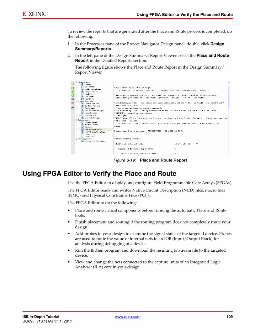
ISE In-Depth Tutorial www.xilinx.com 109UG695 (v13.1) March 1, 2011
Using FPGA Editor to Verify the Place and Route
To review the reports that are generated after the Place and Route process is completed, do the following:
1. In the Processes pane of the Project Navigator Design panel, double-click Design Summary/Reports.
2. In the left pane of the Design Summary/Report Viewer, select the Place and Route Report in the Detailed Reports section.
The following figure shows the Place and Route Report in the Design Summary/Report Viewer.
Using FPGA Editor to Verify the Place and RouteUse the FPGA Editor to display and configure Field Programmable Gate Arrays (FPGAs).
The FPGA Editor reads and writes Native Circuit Description (NCD) files, macro files (NMC) and Physical Constraints Files (PCF).
Use FPGA Editor to do the following:
• Place and route critical components before running the automatic Place and Route tools.
• Finish placement and routing if the routing program does not completely route your design.
• Add probes to your design to examine the signal states of the targeted device. Probes are used to route the value of internal nets to an IOB (Input/Output Block) for analysis during debugging of a device.
• Run the BitGen program and download the resulting bitstream file to the targeted device.
• View and change the nets connected to the capture units of an Integrated Logic Analyzer (ILA) core in your design.
X-Ref Target - Figure 6-19
Figure 6-19: Place and Route Report
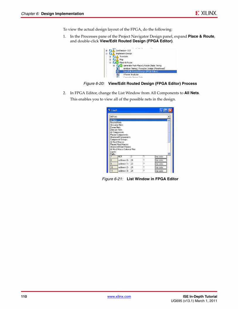
110 www.xilinx.com ISE In-Depth TutorialUG695 (v13.1) March 1, 2011
Chapter 6: Design Implementation
To view the actual design layout of the FPGA, do the following:
1. In the Processes pane of the Project Navigator Design panel, expand Place & Route, and double-click View/Edit Routed Design (FPGA Editor).
2. In FPGA Editor, change the List Window from All Components to All Nets.
This enables you to view all of the possible nets in the design.
X-Ref Target - Figure 6-20
Figure 6-20: View/Edit Routed Design (FPGA Editor) Process
X-Ref Target - Figure 6-21
Figure 6-21: List Window in FPGA Editor
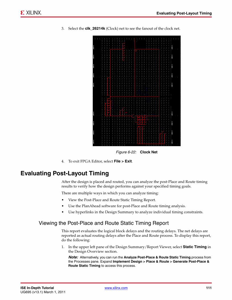
ISE In-Depth Tutorial www.xilinx.com 111UG695 (v13.1) March 1, 2011
Evaluating Post-Layout Timing
3. Select the clk_26214k (Clock) net to see the fanout of the clock net.
4. To exit FPGA Editor, select File > Exit.
Evaluating Post-Layout TimingAfter the design is placed and routed, you can analyze the post-Place and Route timing results to verify how the design performs against your specified timing goals.
There are multiple ways in which you can analyze timing:
• View the Post-Place and Route Static Timing Report.
• Use the PlanAhead software for post-Place and Route timing analysis.
• Use hyperlinks in the Design Summary to analyze individual timing constraints.
Viewing the Post-Place and Route Static Timing ReportThis report evaluates the logical block delays and the routing delays. The net delays are reported as actual routing delays after the Place and Route process. To display this report, do the following:
1. In the upper left pane of the Design Summary/Report Viewer, select Static Timing in the Design Overview section.
Note: Alternatively, you can run the Analyze Post-Place & Route Static Timing process from the Processes pane. Expand Implement Design > Place & Route > Generate Post-Place & Route Static Timing to access this process.
X-Ref Target - Figure 6-22
Figure 6-22: Clock Net
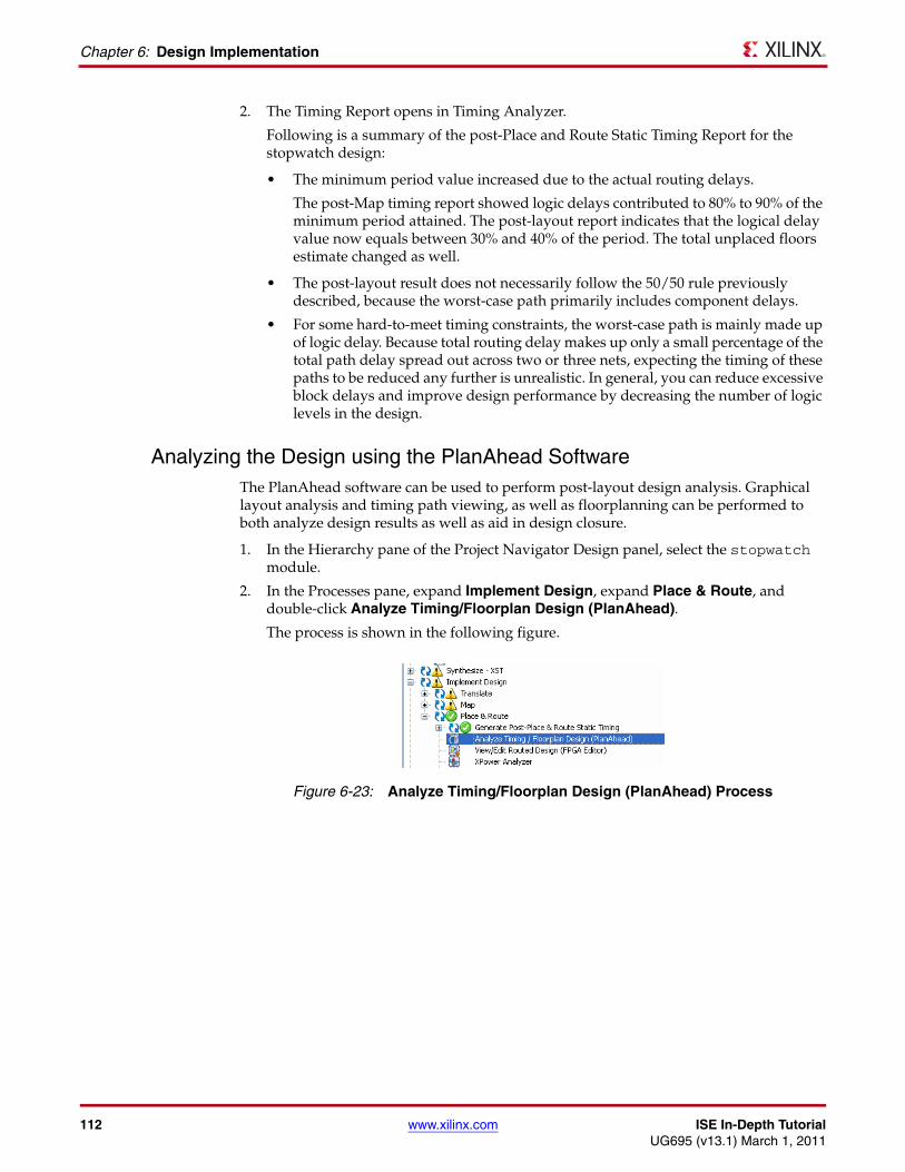
112 www.xilinx.com ISE In-Depth TutorialUG695 (v13.1) March 1, 2011
Chapter 6: Design Implementation
2. The Timing Report opens in Timing Analyzer.
Following is a summary of the post-Place and Route Static Timing Report for the stopwatch design:
• The minimum period value increased due to the actual routing delays.
The post-Map timing report showed logic delays contributed to 80% to 90% of the minimum period attained. The post-layout report indicates that the logical delay value now equals between 30% and 40% of the period. The total unplaced floors estimate changed as well.
• The post-layout result does not necessarily follow the 50/50 rule previously described, because the worst-case path primarily includes component delays.
• For some hard-to-meet timing constraints, the worst-case path is mainly made up of logic delay. Because total routing delay makes up only a small percentage of the total path delay spread out across two or three nets, expecting the timing of these paths to be reduced any further is unrealistic. In general, you can reduce excessive block delays and improve design performance by decreasing the number of logic levels in the design.
Analyzing the Design using the PlanAhead SoftwareThe PlanAhead software can be used to perform post-layout design analysis. Graphical layout analysis and timing path viewing, as well as floorplanning can be performed to both analyze design results as well as aid in design closure.
1. In the Hierarchy pane of the Project Navigator Design panel, select the stopwatch module.
2. In the Processes pane, expand Implement Design, expand Place & Route, and double-click Analyze Timing/Floorplan Design (PlanAhead).
The process is shown in the following figure.X-Ref Target - Figure 6-23
Figure 6-23: Analyze Timing/Floorplan Design (PlanAhead) Process
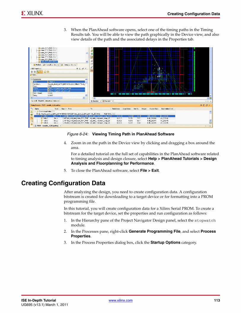
ISE In-Depth Tutorial www.xilinx.com 113UG695 (v13.1) March 1, 2011
Creating Configuration Data
3. When the PlanAhead software opens, select one of the timing paths in the Timing Results tab. You will be able to view the path graphically in the Device view, and also view details of the path and the associated delays in the Properties tab.
4. Zoom in on the path in the Device view by clicking and dragging a box around the area.
For a detailed tutorial on the full set of capabilities in the PlanAhead software related to timing analysis and design closure, select Help > PlanAhead Tutorials > Design Analysis and Floorplanning for Performance.
5. To close the PlanAhead software, select File > Exit.
Creating Configuration DataAfter analyzing the design, you need to create configuration data. A configuration bitstream is created for downloading to a target device or for formatting into a PROM programming file.
In this tutorial, you will create configuration data for a Xilinx Serial PROM. To create a bitstream for the target device, set the properties and run configuration as follows:
1. In the Hierarchy pane of the Project Navigator Design panel, select the stopwatch module.
2. In the Processes pane, right-click Generate Programming File, and select Process Properties.
3. In the Process Properties dialog box, click the Startup Options category.
X-Ref Target - Figure 6-24
Figure 6-24: Viewing Timing Path in PlanAhead Software
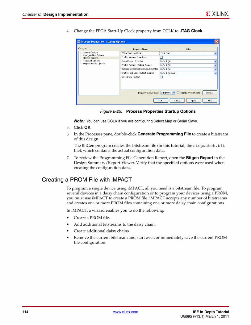
114 www.xilinx.com ISE In-Depth TutorialUG695 (v13.1) March 1, 2011
Chapter 6: Design Implementation
4. Change the FPGA Start-Up Clock property from CCLK to JTAG Clock.
Note: You can use CCLK if you are configuring Select Map or Serial Slave.
5. Click OK.
6. In the Processes pane, double-click Generate Programming File to create a bitstream of this design.
The BitGen program creates the bitstream file (in this tutorial, the stopwatch.bit file), which contains the actual configuration data.
7. To review the Programming File Generation Report, open the Bitgen Report in the Design Summary/Report Viewer. Verify that the specified options were used when creating the configuration data.
Creating a PROM File with iMPACTTo program a single device using iMPACT, all you need is a bitstream file. To program several devices in a daisy chain configuration or to program your devices using a PROM, you must use iMPACT to create a PROM file. iMPACT accepts any number of bitstreams and creates one or more PROM files containing one or more daisy chain configurations.
In iMPACT, a wizard enables you to do the following:
• Create a PROM file.
• Add additional bitstreams to the daisy chain.
• Create additional daisy chains.
• Remove the current bitstream and start over, or immediately save the current PROM file configuration.
X-Ref Target - Figure 6-25
Figure 6-25: Process Properties Startup Options
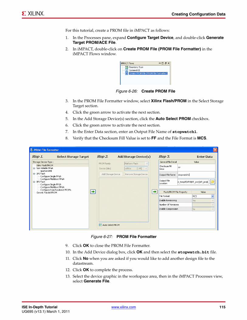
ISE In-Depth Tutorial www.xilinx.com 115UG695 (v13.1) March 1, 2011
Creating Configuration Data
For this tutorial, create a PROM file in iMPACT as follows:
1. In the Processes pane, expand Configure Target Device, and double-click Generate Target PROM/ACE File.
2. In iMPACT, double-click on Create PROM File (PROM File Formatter) in the iMPACT Flows window.
3. In the PROM File Formatter window, select Xilinx Flash/PROM in the Select Storage Target section.
4. Click the green arrow to activate the next section.
5. In the Add Storage Device(s) section, click the Auto Select PROM checkbox.
6. Click the green arrow to activate the next section.
7. In the Enter Data section, enter an Output File Name of stopwatch1.
8. Verify that the Checksum Fill Value is set to FF and the File Format is MCS.
9. Click OK to close the PROM File Formatter.
10. In the Add Device dialog box, click OK and then select the stopwatch.bit file.
11. Click No when you are asked if you would like to add another design file to the datastream.
12. Click OK to complete the process.
13. Select the device graphic in the workspace area, then in the iMPACT Processes view, select Generate File.
X-Ref Target - Figure 6-26
Figure 6-26: Create PROM File
X-Ref Target - Figure 6-27
Figure 6-27: PROM File Formatter
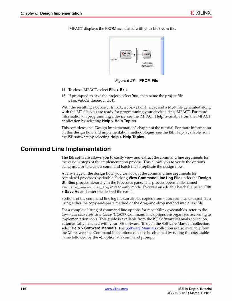
116 www.xilinx.com ISE In-Depth TutorialUG695 (v13.1) March 1, 2011
Chapter 6: Design Implementation
iMPACT displays the PROM associated with your bitstream file.
14. To close iMPACT, select File > Exit.
15. If prompted to save the project, select Yes, then name the project file stopwatch_impact.ipf.
With the resulting stopwatch.bit, stopwatch1.mcs, and a MSK file generated along with the BIT file, you are ready for programming your device using iMPACT. For more information on programming a device, see the iMPACT Help, available from the iMPACT application by selecting Help > Help Topics.
This completes the “Design Implementation” chapter of the tutorial. For more information on this design flow and implementation methodologies, see the ISE Help, available from the ISE software by selecting Help > Help Topics.
Command Line ImplementationThe ISE software allows you to easily view and extract the command line arguments for the various steps of the implementation process. This allows you to verify the options being used or to create a command batch file to replicate the design flow.
At any stage of the design flow, you can look at the command line arguments for completed processes by double-clicking View Command Line Log File under the Design Utilities process hierarchy in the Processes pane. This process opens a file named <source_name>.cmd_log in read-only mode. To create an editable batch file, select File > Save As and enter the desired file name.
Sections of the command line log file can also be copied from <source_name>.cmd_log using either the copy-and-paste method or the drag-and-drop method into a text file.
For a complete listing of command line options for most Xilinx executables, refer to the Command Line Tools User Guide (UG628). Command line options are organized according to implementation tools. This guide is available from the ISE Software Manuals collection, automatically installed with your ISE software. To open the Software Manuals collection, select Help > Software Manuals. The Software Manuals collection is also available from the Xilinx website. Command line options can also be obtained by typing the executable name followed by the -h option at a command prompt.
X-Ref Target - Figure 6-28
Figure 6-28: PROM File
ISE In-Depth Tutorial www.xilinx.com 117UG695 (v13.1) March 1, 2011
Chapter 7
Timing Simulation
Overview of Timing Simulation FlowTiming simulation uses the block and routing delay information from a routed design to give a more accurate assessment of the behavior of the circuit under worst-case conditions. For this reason, timing simulation is performed after the design has been placed and routed.
Timing (post-Place and Route) simulation is a highly recommended part of the HDL design flow for Xilinx® devices. Timing simulation uses the detailed timing and design layout information that is available after Place and Route. This enables simulation of the design, which closely matches the actual device operation. Performing a timing simulation in addition to a static timing analysis will help to uncover issues that cannot be found in a static timing analysis alone. To verify the design, the design should be analyzed both statically and dynamically.
In this chapter, you will perform a timing simulation using either the ModelSim simulator or the Xilinx ISim simulator.
Getting StartedThe following sections outline the requirements to perform this part of the tutorial flow.
Required SoftwareTo simulate with ModelSim, you must have the Xilinx ISE® Design Suite and ModelSim simulator installed. Refer to Chapter 5, Behavioral Simulation, for information on installing and setting up ModelSim. Simulating with ISim requires that the ISE Design Suite software is installed.
118 www.xilinx.com ISE In-Depth TutorialUG695 (v13.1) March 1, 2011
Chapter 7: Timing Simulation
Required FilesThe timing simulation flow requires the following files:
• Design files (VHDL or Verilog)
This chapter assumes that you have completed Chapter 6, Design Implementation, and thus, have a placed and routed design. The NetGen tool will be used in this chapter to create a simulation netlist from the placed and routed design, which will be used to represent the design during the timing simulation.
• Test bench file (VHDL or Verilog)
To simulate the design, a test bench is needed to provide stimulus to the design. You should use the same test bench that was used to perform the behavioral simulation. Please refer to Adding an HDL Test Bench in Chapter 5 if you do not already have a test bench in your project.
• Xilinx simulation libraries
For timing simulation, the SIMPRIM library is needed to simulate the design.
To perform timing simulation of Xilinx designs in any HDL simulator, the SIMPRIM library must be set up correctly. The timing simulation netlist created by Xilinx is composed entirely of instantiated primitives, which are modeled in the SIMPRIM library.
If you completed Chapter 5, Behavioral Simulation, the SIMPRIM library should already be compiled. For more information on compiling and setting up Xilinx simulation libraries, see Xilinx Simulation Libraries in Chapter 5.
Specifying a SimulatorTo specify the simulator to simulate the stopwatch design, do the following:
1. In the Hierarchy pane of the Project Navigator Design panel, right-click the device line (xc3s700A-4fg484), and select Design Properties.
2. In the Design Properties dialog box, set the Simulator field to ISim (VHDL/Verilog) or ModelSim (with the appropriate type and language).
Note: ModelSim and Xilinx ISim are the only simulators that are integrated with Project Navigator. Selecting a different simulator (for example, NC-Sim or VCS) will set the correct options for NetGen to create a simulation netlist for that simulator, but Project Navigator will not directly open the simulator. For additional information about simulation and for a list of other supported simulators, see the Synthesis and Simulation Design Guide (UG626). This guide is available from the ISE Software Manuals collection, automatically installed with your ISE software. To open the Software Manuals collection, select Help > Software Manuals. The Software Manuals collection is also available from the Xilinx website.
Timing Simulation Using ModelSimThe Xilinx ISE software provides an integrated flow with the Mentor ModelSim simulator. The ISE software enables you to create work directories, compile source files, initialize simulation, and control simulation properties for ModelSim.
Note: To simulate with ISim, skip to Timing Simulation Using Xilinx ISim. Whether you choose to use the ModelSim simulator or ISim for this tutorial, the end result is the same.
ISE In-Depth Tutorial www.xilinx.com 119UG695 (v13.1) March 1, 2011
Timing Simulation Using ModelSim
Specifying Simulation Process PropertiesTo set the simulation process properties, do the following:
1. In the View pane of the Project Navigator Design panel, select Simulation, and select Post-Route from the drop-down list.
2. In the Hierarchy pane, select the test bench file (stopwatch_tb).
3. In the Processes pane, expand ModelSim Simulator, right-click Simulate Post-Place & Route Model, and select Process Properties.
Note: If the ModelSim Simulator processes do not appear, ensure that you selected ModelSim in the Design Properties dialog box, as described in Specifying a Simulator. If this setting is correct and the ModelSim Simulator processes still do not appear, ensure that Project Navigator can find the modelsim.exe file. To set the location for this file, select Edit > Preferences. In the left pane of the Preferences dialog box, expand ISE General, and click Integrated Tools. In the right pane, under Model Tech Simulator, browse to the location of modelsim.exe file. For example: c:\modeltech_xe\win32xoem\modelsim.exe.
4. In the Process Properties dialog box, ensure that the Property display level is set to Advanced.
This global setting enables you to see all available properties.
5. Select the Simulation Model Properties category. These properties set the options that NetGen uses when generating the simulation netlist. For a description of each property, click the Help button.
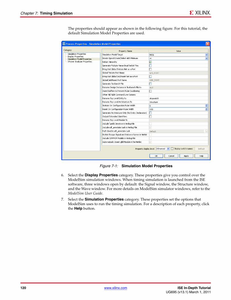
120 www.xilinx.com ISE In-Depth TutorialUG695 (v13.1) March 1, 2011
Chapter 7: Timing Simulation
The properties should appear as shown in the following figure. For this tutorial, the default Simulation Model Properties are used.
6. Select the Display Properties category. These properties give you control over the ModelSim simulation windows. When timing simulation is launched from the ISE software, three windows open by default: the Signal window, the Structure window, and the Wave window. For more details on ModelSim simulator windows, refer to the ModelSim User Guide.
7. Select the Simulation Properties category. These properties set the options that ModelSim uses to run the timing simulation. For a description of each property, click the Help button.
X-Ref Target - Figure 7-1
Figure 7-1: Simulation Model Properties
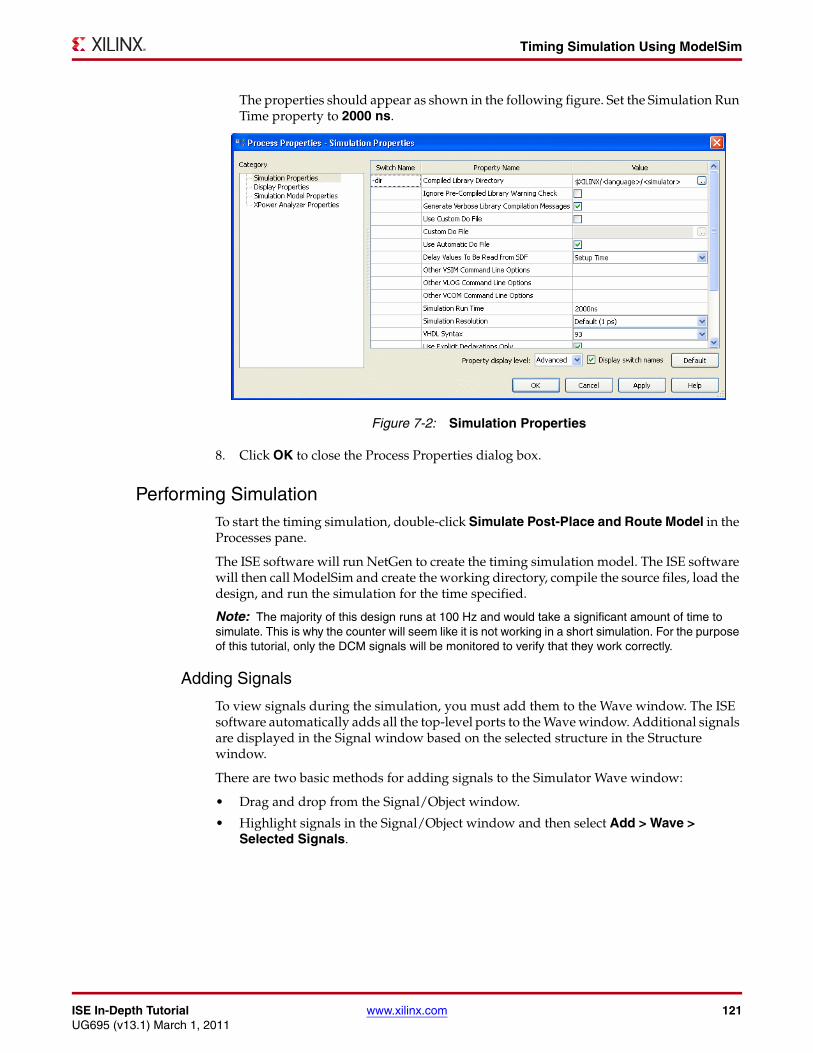
ISE In-Depth Tutorial www.xilinx.com 121UG695 (v13.1) March 1, 2011
Timing Simulation Using ModelSim
The properties should appear as shown in the following figure. Set the Simulation Run Time property to 2000 ns.
8. Click OK to close the Process Properties dialog box.
Performing SimulationTo start the timing simulation, double-click Simulate Post-Place and Route Model in the Processes pane.
The ISE software will run NetGen to create the timing simulation model. The ISE software will then call ModelSim and create the working directory, compile the source files, load the design, and run the simulation for the time specified.
Note: The majority of this design runs at 100 Hz and would take a significant amount of time to simulate. This is why the counter will seem like it is not working in a short simulation. For the purpose of this tutorial, only the DCM signals will be monitored to verify that they work correctly.
Adding Signals
To view signals during the simulation, you must add them to the Wave window. The ISE software automatically adds all the top-level ports to the Wave window. Additional signals are displayed in the Signal window based on the selected structure in the Structure window.
There are two basic methods for adding signals to the Simulator Wave window:
• Drag and drop from the Signal/Object window.
• Highlight signals in the Signal/Object window and then select Add > Wave > Selected Signals.
X-Ref Target - Figure 7-2
Figure 7-2: Simulation Properties
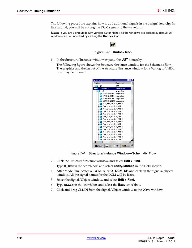
122 www.xilinx.com ISE In-Depth TutorialUG695 (v13.1) March 1, 2011
Chapter 7: Timing Simulation
The following procedure explains how to add additional signals in the design hierarchy. In this tutorial, you will be adding the DCM signals to the waveform.
Note: If you are using ModelSim version 6.0 or higher, all the windows are docked by default. All windows can be undocked by clicking the Undock icon.
1. In the Structure/Instance window, expand the UUT hierarchy.
The following figure shows the Structure/Instance window for the Schematic flow. The graphics and the layout of the Structure/Instance window for a Verilog or VHDL flow may be different.
2. Click the Structure/Instance window, and select Edit > Find.
3. Type X_DCM in the search box, and select Entity/Module in the Field section.
4. After ModelSim locates X_DCM, select X_DCM_SP, and click on the signals/objects window. All the signal names for the DCM will be listed.
5. Select the Signal/Object window, and select Edit > Find.
6. Type CLKIN in the search box and select the Exact checkbox.
7. Click and drag CLKIN from the Signal/Object window to the Wave window.
X-Ref Target - Figure 7-3
Figure 7-3: Undock Icon
X-Ref Target - Figure 7-4
Figure 7-4: Structure/Instance Window—Schematic Flow
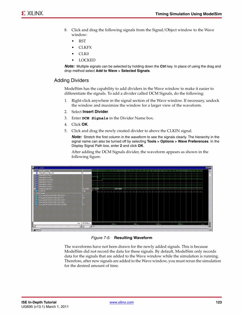
ISE In-Depth Tutorial www.xilinx.com 123UG695 (v13.1) March 1, 2011
Timing Simulation Using ModelSim
8. Click and drag the following signals from the Signal/Object window to the Wave window:
• RST
• CLKFX
• CLK0
• LOCKED
Note: Multiple signals can be selected by holding down the Ctrl key. In place of using the drag and drop method select Add to Wave > Selected Signals.
Adding Dividers
ModelSim has the capability to add dividers in the Wave window to make it easier to differentiate the signals. To add a divider called DCM Signals, do the following:
1. Right-click anywhere in the signal section of the Wave window. If necessary, undock the window and maximize the window for a larger view of the waveform.
2. Select Insert Divider.
3. Enter DCM Signals in the Divider Name box.
4. Click OK.
5. Click and drag the newly created divider to above the CLKIN signal.
Note: Stretch the first column in the waveform to see the signals clearly. The hierarchy in the signal name can also be turned off by selecting Tools > Options > Wave Preferences. In the Display Signal Path box, enter 2 and click OK.
After adding the DCM Signals divider, the waveform appears as shown in the following figure.
The waveforms have not been drawn for the newly added signals. This is because ModelSim did not record the data for these signals. By default, ModelSim only records data for the signals that are added to the Wave window while the simulation is running. Therefore, after new signals are added to the Wave window, you must rerun the simulation for the desired amount of time.
X-Ref Target - Figure 7-5
Figure 7-5: Resulting Waveform
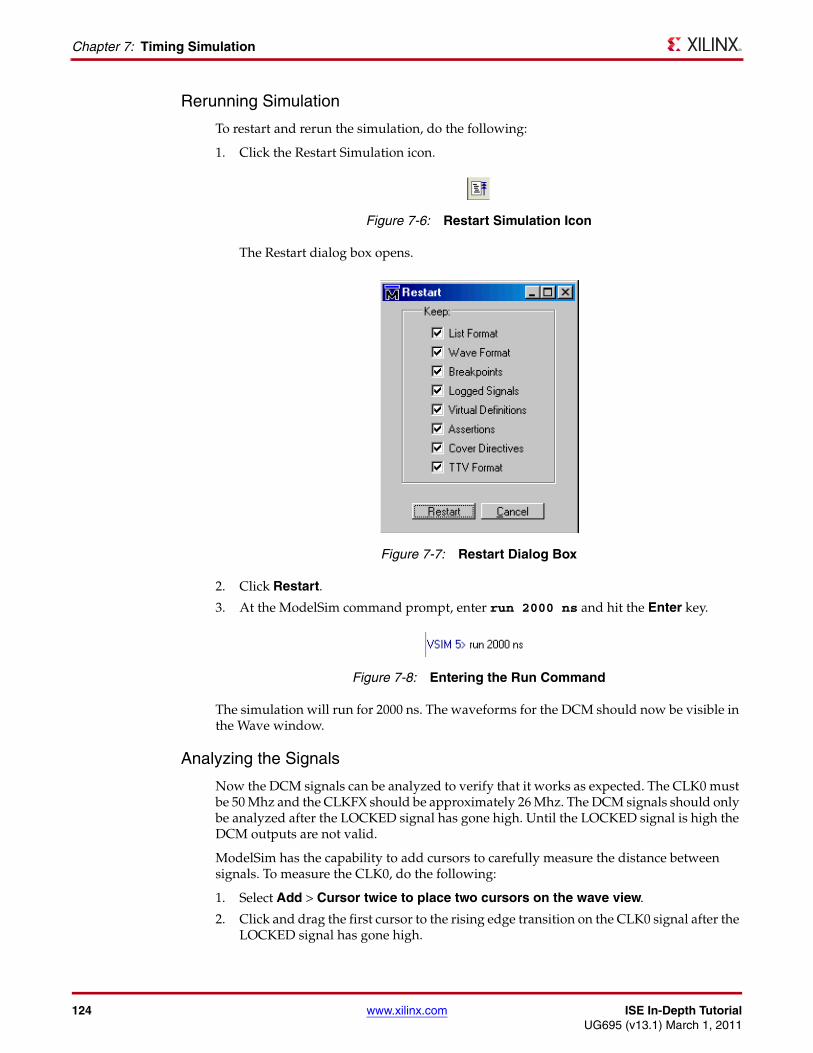
124 www.xilinx.com ISE In-Depth TutorialUG695 (v13.1) March 1, 2011
Chapter 7: Timing Simulation
Rerunning Simulation
To restart and rerun the simulation, do the following:
1. Click the Restart Simulation icon.
The Restart dialog box opens.
2. Click Restart.
3. At the ModelSim command prompt, enter run 2000 ns and hit the Enter key.
The simulation will run for 2000 ns. The waveforms for the DCM should now be visible in the Wave window.
Analyzing the Signals
Now the DCM signals can be analyzed to verify that it works as expected. The CLK0 must be 50 Mhz and the CLKFX should be approximately 26 Mhz. The DCM signals should only be analyzed after the LOCKED signal has gone high. Until the LOCKED signal is high the DCM outputs are not valid.
ModelSim has the capability to add cursors to carefully measure the distance between signals. To measure the CLK0, do the following:
1. Select Add > Cursor twice to place two cursors on the wave view.
2. Click and drag the first cursor to the rising edge transition on the CLK0 signal after the LOCKED signal has gone high.
X-Ref Target - Figure 7-6
Figure 7-6: Restart Simulation Icon
X-Ref Target - Figure 7-7
Figure 7-7: Restart Dialog Box
X-Ref Target - Figure 7-8
Figure 7-8: Entering the Run Command
ISE In-Depth Tutorial www.xilinx.com 125UG695 (v13.1) March 1, 2011
Timing Simulation Using ModelSim
3. Click and drag the second cursor to a position just right of the first cursor on the CLK0 signal.
4. Click the Find Next Transition icon twice to move the cursor to the next rising edge on the CLK0 signal.
Look at the bottom of the waveform to view the distance between the two cursors. The measurement should read 20000 ps. This converts to 50 Mhz, which is the input frequency from the test bench, which in turn should be the DCM CLK0 output.
Measure CLKFX using the same steps as above. The measurement should read 38462 ps. This equals approximately 26 Mhz.
Saving the Simulation
The ModelSim simulator provides the capability of saving the signals list in the Wave window. Save the signals list after new signals or stimuli are added, and after simulation is rerun. The saved signals list can easily be loaded each time the simulation is started. To save the signals list, do the following:
1. In the Wave window, select File > Save Format.
2. In the Save Format dialog box, rename the filename from the default wave.do to dcm_signal_tim.do.
3. Click OK.
After restarting the simulation, you can select File > Load in the Wave window to reload this file.
Your timing simulation is complete, and you are ready to program your device by following Chapter 8, Configuration Using iMPACT.
X-Ref Target - Figure 7-9
Figure 7-9: Find Next Transition Icon
X-Ref Target - Figure 7-10
Figure 7-10: Save Format Dialog Box
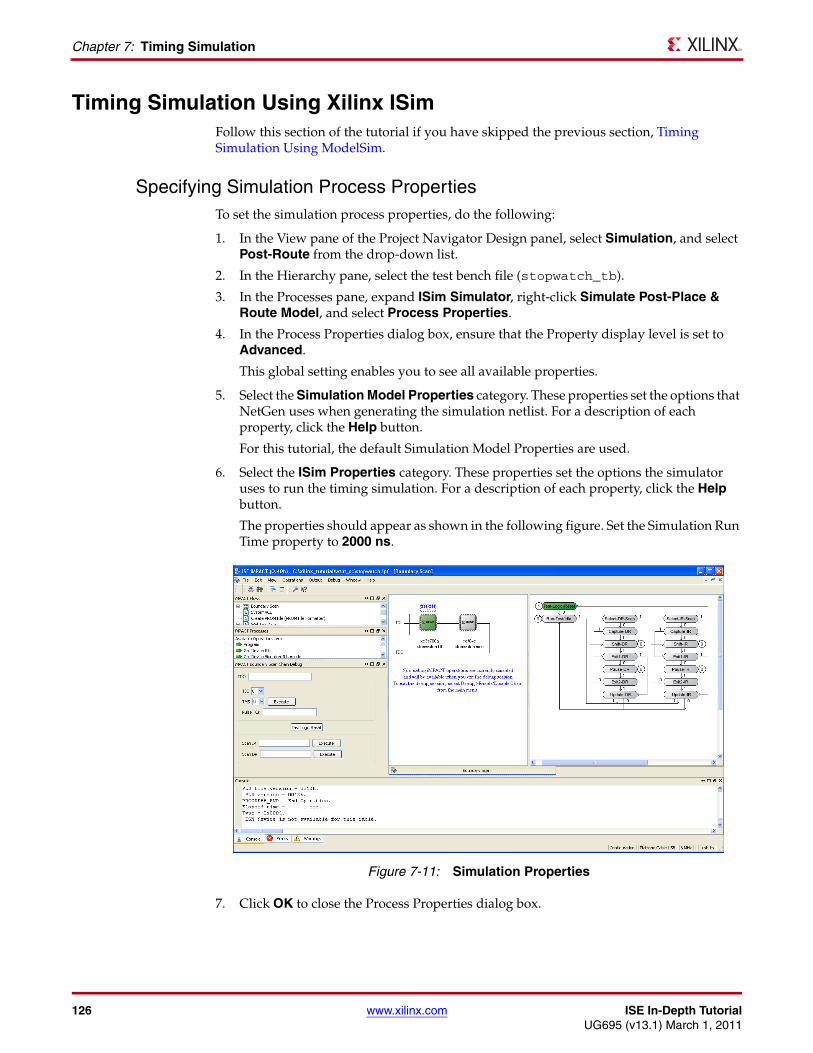
126 www.xilinx.com ISE In-Depth TutorialUG695 (v13.1) March 1, 2011
Chapter 7: Timing Simulation
Timing Simulation Using Xilinx ISimFollow this section of the tutorial if you have skipped the previous section, Timing Simulation Using ModelSim.
Specifying Simulation Process PropertiesTo set the simulation process properties, do the following:
1. In the View pane of the Project Navigator Design panel, select Simulation, and select Post-Route from the drop-down list.
2. In the Hierarchy pane, select the test bench file (stopwatch_tb).
3. In the Processes pane, expand ISim Simulator, right-click Simulate Post-Place & Route Model, and select Process Properties.
4. In the Process Properties dialog box, ensure that the Property display level is set to Advanced.
This global setting enables you to see all available properties.
5. Select the Simulation Model Properties category. These properties set the options that NetGen uses when generating the simulation netlist. For a description of each property, click the Help button.
For this tutorial, the default Simulation Model Properties are used.
6. Select the ISim Properties category. These properties set the options the simulator uses to run the timing simulation. For a description of each property, click the Help button.
The properties should appear as shown in the following figure. Set the Simulation Run Time property to 2000 ns.
7. Click OK to close the Process Properties dialog box.
X-Ref Target - Figure 7-11
Figure 7-11: Simulation Properties
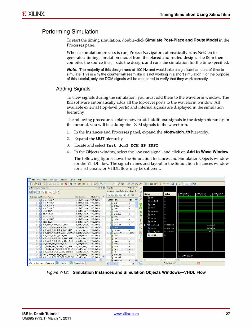
ISE In-Depth Tutorial www.xilinx.com 127UG695 (v13.1) March 1, 2011
Timing Simulation Using Xilinx ISim
Performing SimulationTo start the timing simulation, double-click Simulate Post-Place and Route Model in the Processes pane.
When a simulation process is run, Project Navigator automatically runs NetGen to generate a timing simulation model from the placed and routed design. The ISim then compiles the source files, loads the design, and runs the simulation for the time specified.
Note: The majority of this design runs at 100 Hz and would take a significant amount of time to simulate. This is why the counter will seem like it is not working in a short simulation. For the purpose of this tutorial, only the DCM signals will be monitored to verify that they work correctly.
Adding Signals
To view signals during the simulation, you must add them to the waveform window. The ISE software automatically adds all the top-level ports to the waveform window. All available external (top-level ports) and internal signals are displayed in the simulation hierarchy.
The following procedure explains how to add additional signals in the design hierarchy. In this tutorial, you will be adding the DCM signals to the waveform.
1. In the Instances and Processes panel, expand the stopwatch_tb hierarchy.
2. Expand the UUT hierarchy.
3. Locate and select Inst_dcm1_DCM_SP_INST
4. In the Objects window, select the locked signal, and click on Add to Wave Window.
The following figure shows the Simulation Instances and Simulation Objects window for the VHDL flow. The signal names and layout in the Simulation Instances window for a schematic or VHDL flow may be different.
X-Ref Target - Figure 7-12
Figure 7-12: Simulation Instances and Simulation Objects Windows—VHDL Flow
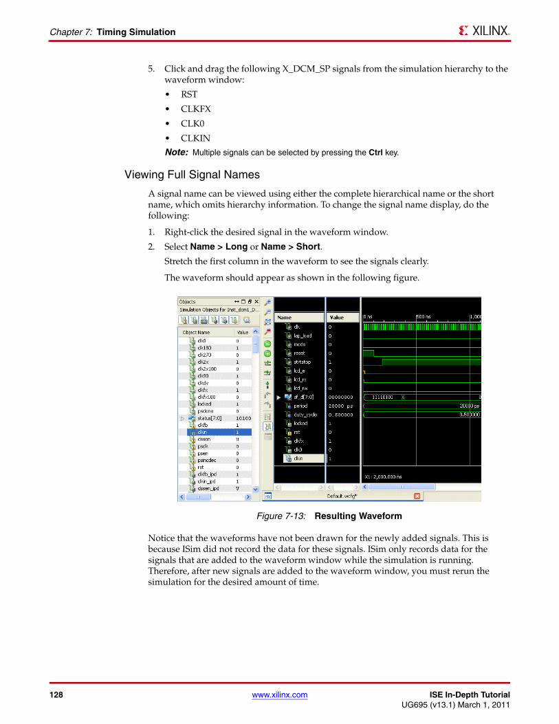
128 www.xilinx.com ISE In-Depth TutorialUG695 (v13.1) March 1, 2011
Chapter 7: Timing Simulation
5. Click and drag the following X_DCM_SP signals from the simulation hierarchy to the waveform window:
• RST
• CLKFX
• CLK0
• CLKIN
Note: Multiple signals can be selected by pressing the Ctrl key.
Viewing Full Signal Names
A signal name can be viewed using either the complete hierarchical name or the short name, which omits hierarchy information. To change the signal name display, do the following:
1. Right-click the desired signal in the waveform window.
2. Select Name > Long or Name > Short.
Stretch the first column in the waveform to see the signals clearly.
The waveform should appear as shown in the following figure.
Notice that the waveforms have not been drawn for the newly added signals. This is because ISim did not record the data for these signals. ISim only records data for the signals that are added to the waveform window while the simulation is running. Therefore, after new signals are added to the waveform window, you must rerun the simulation for the desired amount of time.
X-Ref Target - Figure 7-13
Figure 7-13: Resulting Waveform
ISE In-Depth Tutorial www.xilinx.com 129UG695 (v13.1) March 1, 2011
Timing Simulation Using Xilinx ISim
Rerunning Simulation
To restart and rerun the simulation, do the following:
1. Click the Restart Simulation toolbar button.
2. At the Sim Console command prompt, enter run 2000 ns and hit the Enter key.
The simulation will run for 2000 ns. The waveforms for the DCM should now be visible in the Simulation window.
Analyzing the Signals
Now the DCM signals can be analyzed to verify that they are working as expected. The CLK0 must be 50 Mhz and the CLKFX should be approximately 26 Mhz. The DCM signals should only be analyzed after the LOCKED signal has gone high. Until the LOCKED signal is high the DCM outputs are not valid.
ISim has the capability to add cursors to carefully measure the distance between signals. To measure the CLK0, do the following:
1. If necessary, zoom in on the waveform using the local Zoom toolbar buttons.
2. In the local waveform viewer toolbar, click the Snap to Transition toolbar button.
3. Click on the first rising edge transition on the CLK0 signal after the LOCKED signal has gone high, then drag the cursor to the right to the next rising edge transition of the CLK0 signal.
At the bottom of the waveform window, the start point time, end point time, and delta times are shown. The delta should read 20.0 ns. This converts to 50 Mhz, which is
X-Ref Target - Figure 7-14
Figure 7-14: Restart Simulation Icon
X-Ref Target - Figure 7-15
Figure 7-15: Entering the Run Command
X-Ref Target - Figure 7-16
Figure 7-16: Snap to Transition Toolbar Button
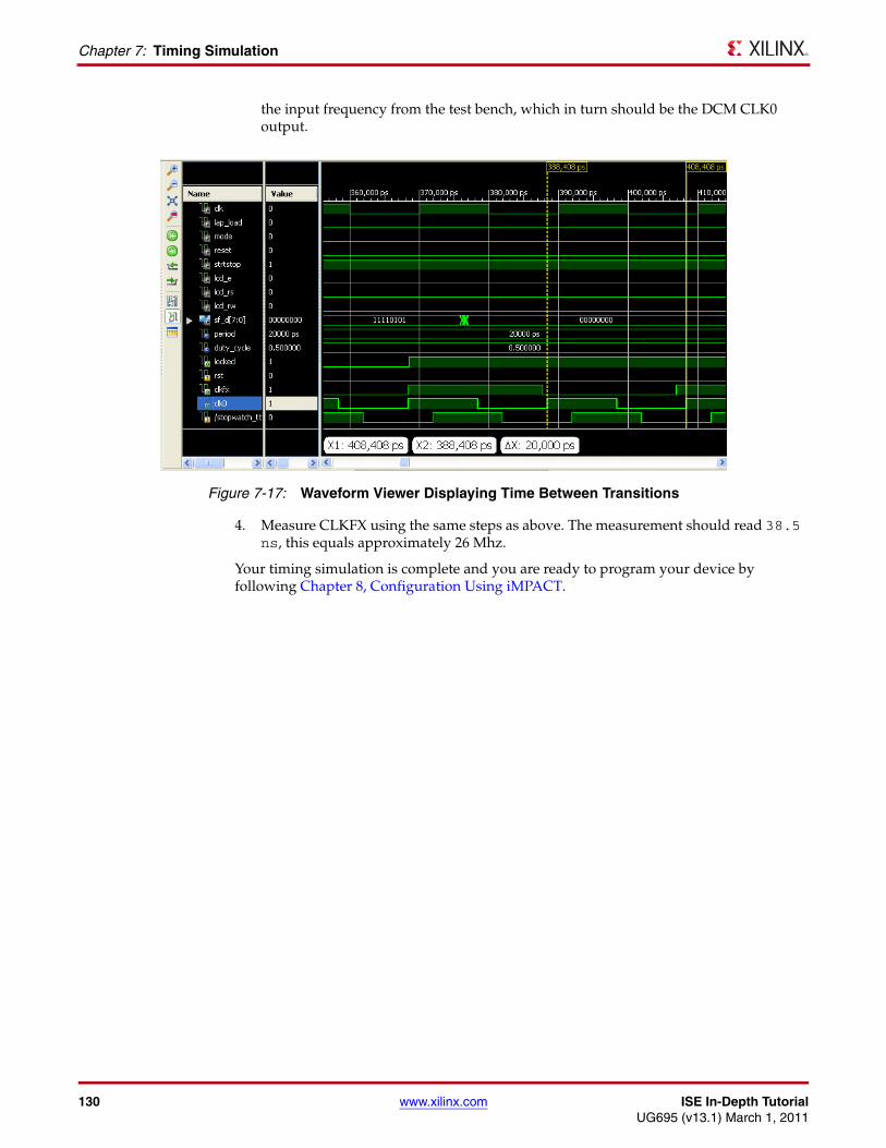
130 www.xilinx.com ISE In-Depth TutorialUG695 (v13.1) March 1, 2011
Chapter 7: Timing Simulation
the input frequency from the test bench, which in turn should be the DCM CLK0 output.
4. Measure CLKFX using the same steps as above. The measurement should read 38.5 ns, this equals approximately 26 Mhz.
Your timing simulation is complete and you are ready to program your device by following Chapter 8, Configuration Using iMPACT.
X-Ref Target - Figure 7-17
Figure 7-17: Waveform Viewer Displaying Time Between Transitions
ISE In-Depth Tutorial www.xilinx.com 131UG695 (v13.1) March 1, 2011
Chapter 8
Configuration Using iMPACT
Overview of iMPACTThis chapter takes you on a tour of iMPACT, a file generation and device programming tool. iMPACT enables you to program through several parallel cables, including the Platform Cable USB. iMPACT can create bitstream files, System ACE™ solution files, PROM files, and SVF/XSVF files. The SVF/XSVF files can be played backed without having to recreate the chain.
Device SupportFor information on supported devices, refer to the ISE Design Suite: Release Notes Guide (UG631) available from the Xilinx® website.
Download Cable SupportThe following cables are supported.
Parallel Cable IVThe Parallel Cable connects to the parallel port of your computer and can be used to facilitate Boundary-Scan functionality. For more information, see the Xilinx Parallel Cable IV Data Sheet available from the Xilinx website.
Platform Cable USBThe Platform Cable connects to the USB port of your computer and can be used to facilitate Boundary-Scan functionality. For more information, see the Platform Cable USB Data Sheet available from the Xilinx website.
Platform Cable USB-IIThe Platform Cable connects to the USB port of your computer and can be used to facilitate Boundary-Scan functionality. For more information, see the Platform Cable USB-II Data Sheet available from the Xilinx website.
Configuration Mode SupportiMPACT currently supports the Boundary-Scan configuration mode for FPGAs, CPLDs, PROMs (XCFxxS and XCFxxP), and third-party SPI/BPI Flash devices.
132 www.xilinx.com ISE In-Depth TutorialUG695 (v13.1) March 1, 2011
Chapter 8: Configuration Using iMPACT
Getting StartedThe following sections outline the requirements to perform this part of the tutorial flow.
Generating the Configuration FilesTo follow this chapter, you must have the following files for the stopwatch design:
• BIT file
A binary file that contains proprietary header information as well as configuration data.
• MCS file
An ASCII file that contains PROM configuration information.
• MSK file
A binary file that contains the same configuration commands as a BIT file, but that has mask data in place of configuration data. This data is not used to configure the device, but is used for verification. If a mask bit is 0, the bit should be verified against the bit stream data. If a mask bit is 1, the bit should not be verified. This file is generated along with the BIT file.
These files are generated in Chapter 6, Design Implementation.
The tutorial project files are provided with the ISE Design Suite Tutorials available from the Xilinx website. Download the project files for the VHDL, Verilog, or schematic design flow.
Connecting the Cable Prior to launching iMPACT, connect the parallel side of the cable to your computer’s parallel port, and connect the cable to the Spartan™-3 Starter Kit demo board. Be sure that the board is powered.
Starting the SoftwareThis section describes how to start the iMPACT software from the ISE® software and how to run the iMPACT software standalone.
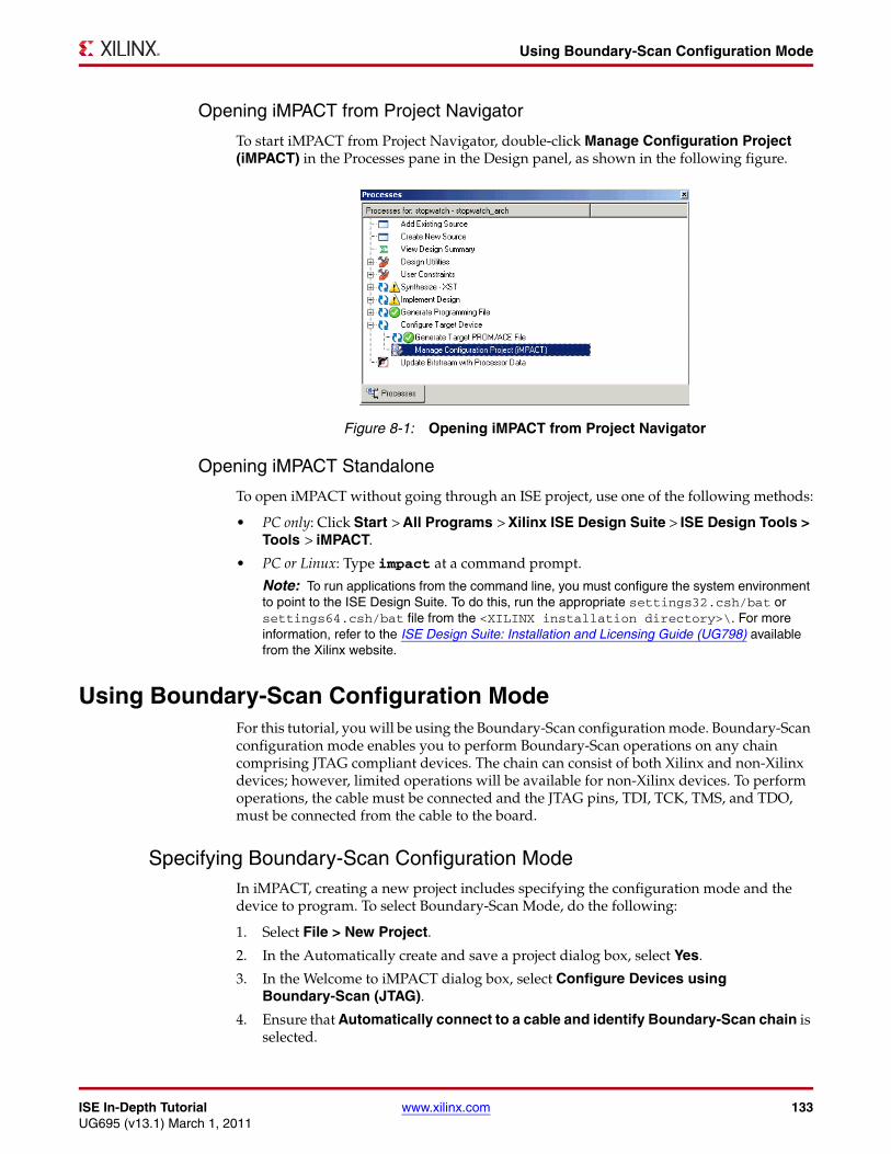
ISE In-Depth Tutorial www.xilinx.com 133UG695 (v13.1) March 1, 2011
Using Boundary-Scan Configuration Mode
Opening iMPACT from Project Navigator
To start iMPACT from Project Navigator, double-click Manage Configuration Project (iMPACT) in the Processes pane in the Design panel, as shown in the following figure.
Opening iMPACT Standalone
To open iMPACT without going through an ISE project, use one of the following methods:
• PC only: Click Start > All Programs > Xilinx ISE Design Suite > ISE Design Tools > Tools > iMPACT.
• PC or Linux: Type impact at a command prompt.
Note: To run applications from the command line, you must configure the system environment to point to the ISE Design Suite. To do this, run the appropriate settings32.csh/bat or settings64.csh/bat file from the <XILINX installation directory>\. For more information, refer to the ISE Design Suite: Installation and Licensing Guide (UG798) available from the Xilinx website.
Using Boundary-Scan Configuration ModeFor this tutorial, you will be using the Boundary-Scan configuration mode. Boundary-Scan configuration mode enables you to perform Boundary-Scan operations on any chain comprising JTAG compliant devices. The chain can consist of both Xilinx and non-Xilinx devices; however, limited operations will be available for non-Xilinx devices. To perform operations, the cable must be connected and the JTAG pins, TDI, TCK, TMS, and TDO, must be connected from the cable to the board.
Specifying Boundary-Scan Configuration ModeIn iMPACT, creating a new project includes specifying the configuration mode and the device to program. To select Boundary-Scan Mode, do the following:
1. Select File > New Project.
2. In the Automatically create and save a project dialog box, select Yes.
3. In the Welcome to iMPACT dialog box, select Configure Devices using Boundary-Scan (JTAG).
4. Ensure that Automatically connect to a cable and identify Boundary-Scan chain is selected.
X-Ref Target - Figure 8-1
Figure 8-1: Opening iMPACT from Project Navigator
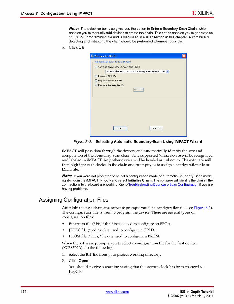
134 www.xilinx.com ISE In-Depth TutorialUG695 (v13.1) March 1, 2011
Chapter 8: Configuration Using iMPACT
Note: The selection box also gives you the option to Enter a Boundary-Scan Chain, which enables you to manually add devices to create the chain. This option enables you to generate an SVF/XSVF programming file and is discussed in a later section in this chapter. Automatically detecting and initializing the chain should be performed whenever possible.
5. Click OK.
iMPACT will pass data through the devices and automatically identify the size and composition of the Boundary-Scan chain. Any supported Xilinx device will be recognized and labeled in iMPACT. Any other device will be labeled as unknown. The software will then highlight each device in the chain and prompt you to assign a configuration file or BSDL file.
Note: If you were not prompted to select a configuration mode or automatic Boundary-Scan mode, right-click in the iMPACT window and select Initialize Chain. The software will identify the chain if the connections to the board are working. Go to Troubleshooting Boundary-Scan Configuration if you are having problems.
Assigning Configuration FilesAfter initializing a chain, the software prompts you for a configuration file (see Figure 8-3). The configuration file is used to program the device. There are several types of configuration files:
• Bitstream file (*.bit, *.rbt, *.isc) is used to configure an FPGA.
• JEDEC file (*.jed,*.isc) is used to configure a CPLD.
• PROM file (*.mcs, *.hex) is used to configure a PROM.
When the software prompts you to select a configuration file for the first device (XC3S700A), do the following:
1. Select the BIT file from your project working directory.
2. Click Open.
You should receive a warning stating that the startup clock has been changed to JtagClk.
X-Ref Target - Figure 8-2
Figure 8-2: Selecting Automatic Boundary-Scan Using iMPACT Wizard
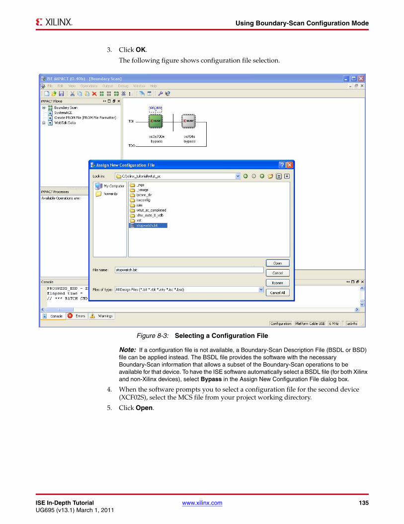
ISE In-Depth Tutorial www.xilinx.com 135UG695 (v13.1) March 1, 2011
Using Boundary-Scan Configuration Mode
3. Click OK.
The following figure shows configuration file selection.
Note: If a configuration file is not available, a Boundary-Scan Description File (BSDL or BSD) file can be applied instead. The BSDL file provides the software with the necessary Boundary-Scan information that allows a subset of the Boundary-Scan operations to be available for that device. To have the ISE software automatically select a BSDL file (for both Xilinx and non-Xilinx devices), select Bypass in the Assign New Configuration File dialog box.
4. When the software prompts you to select a configuration file for the second device (XCF02S), select the MCS file from your project working directory.
5. Click Open.
X-Ref Target - Figure 8-3
Figure 8-3: Selecting a Configuration File
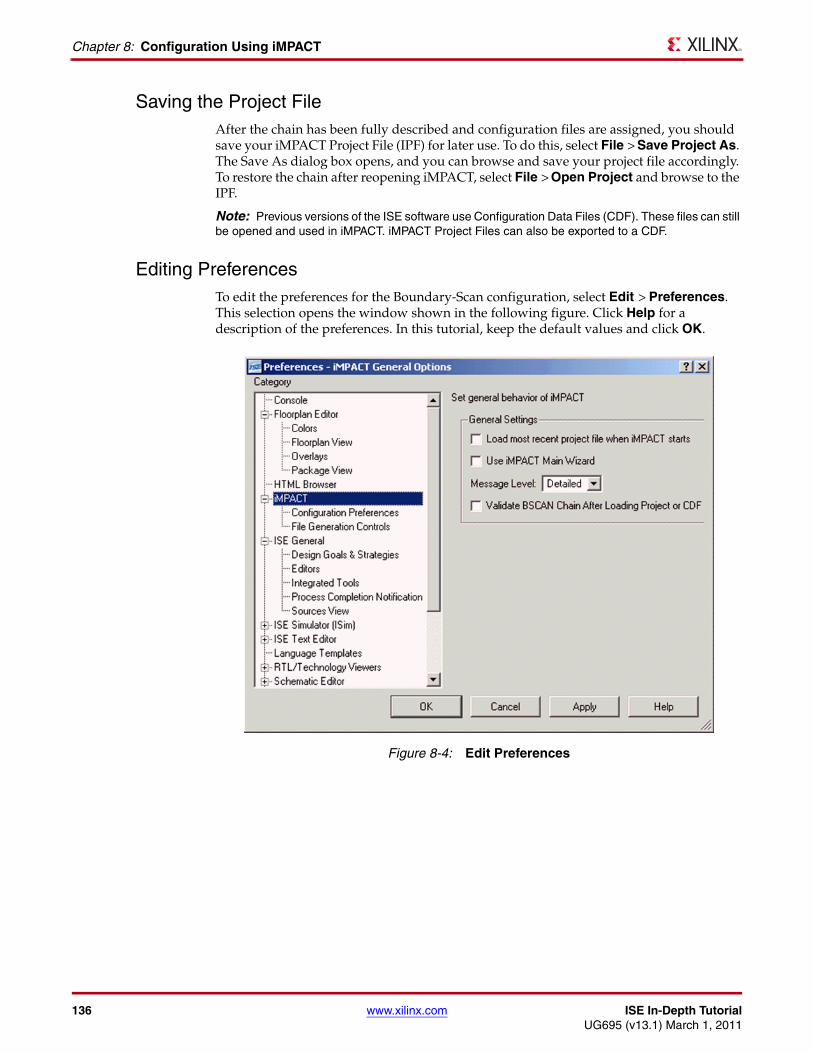
136 www.xilinx.com ISE In-Depth TutorialUG695 (v13.1) March 1, 2011
Chapter 8: Configuration Using iMPACT
Saving the Project FileAfter the chain has been fully described and configuration files are assigned, you should save your iMPACT Project File (IPF) for later use. To do this, select File > Save Project As. The Save As dialog box opens, and you can browse and save your project file accordingly. To restore the chain after reopening iMPACT, select File > Open Project and browse to the IPF.
Note: Previous versions of the ISE software use Configuration Data Files (CDF). These files can still be opened and used in iMPACT. iMPACT Project Files can also be exported to a CDF.
Editing PreferencesTo edit the preferences for the Boundary-Scan configuration, select Edit > Preferences. This selection opens the window shown in the following figure. Click Help for a description of the preferences. In this tutorial, keep the default values and click OK.X-Ref Target - Figure 8-4
Figure 8-4: Edit Preferences
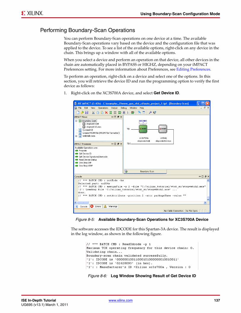
ISE In-Depth Tutorial www.xilinx.com 137UG695 (v13.1) March 1, 2011
Using Boundary-Scan Configuration Mode
Performing Boundary-Scan OperationsYou can perform Boundary-Scan operations on one device at a time. The available Boundary-Scan operations vary based on the device and the configuration file that was applied to the device. To see a list of the available options, right-click on any device in the chain. This brings up a window with all of the available options.
When you select a device and perform an operation on that device, all other devices in the chain are automatically placed in BYPASS or HIGHZ, depending on your iMPACT Preferences setting. For more information about Preferences, see Editing Preferences.
To perform an operation, right-click on a device and select one of the options. In this section, you will retrieve the device ID and run the programming option to verify the first device as follows:
1. Right-click on the XC3S700A device, and select Get Device ID.
The software accesses the IDCODE for this Spartan-3A device. The result is displayed in the log window, as shown in the following figure.
Figure X-Ref Target - Figure 8-5
Figure 8-5: Available Boundary-Scan Operations for XC3S700A Device
X-Ref Target - Figure 8-6
Figure 8-6: Log Window Showing Result of Get Device ID
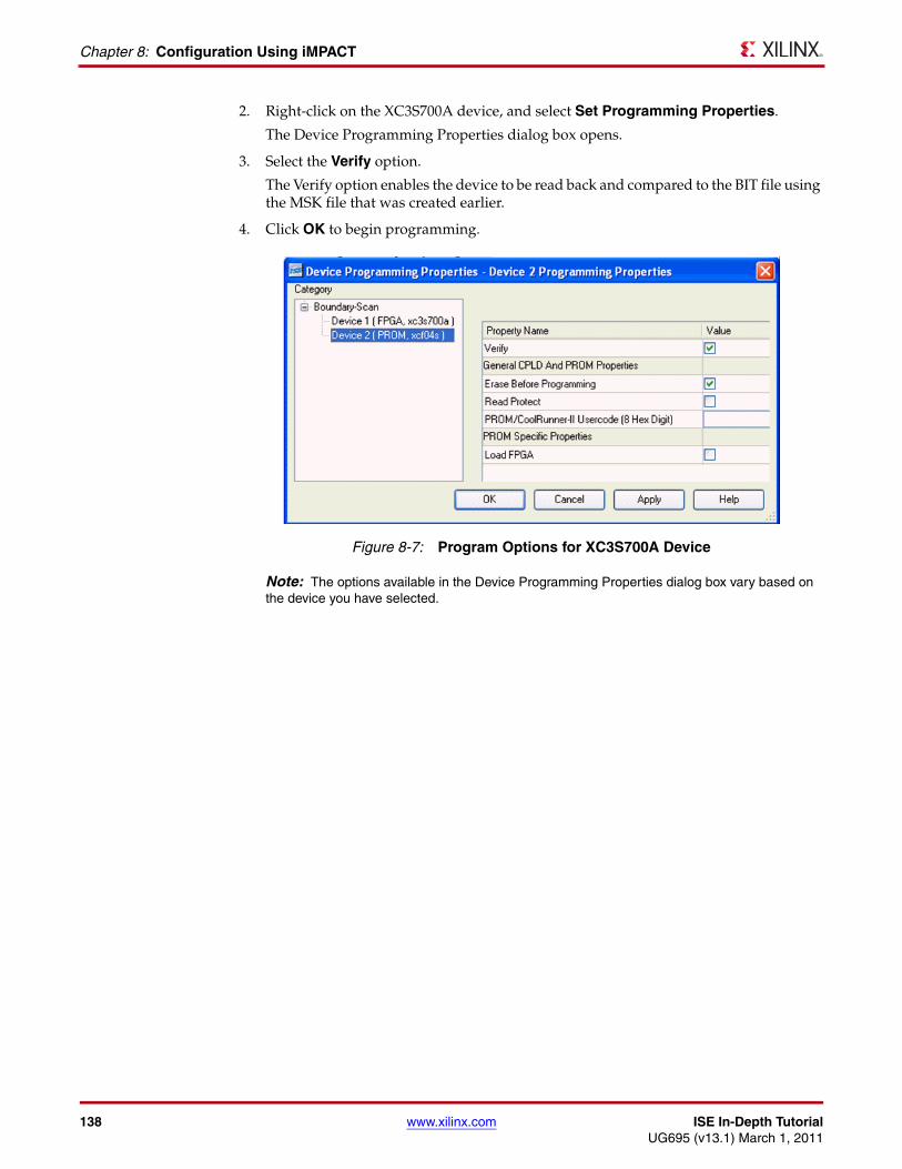
138 www.xilinx.com ISE In-Depth TutorialUG695 (v13.1) March 1, 2011
Chapter 8: Configuration Using iMPACT
2. Right-click on the XC3S700A device, and select Set Programming Properties.
The Device Programming Properties dialog box opens.
3. Select the Verify option.
The Verify option enables the device to be read back and compared to the BIT file using the MSK file that was created earlier.
4. Click OK to begin programming.
Note: The options available in the Device Programming Properties dialog box vary based on the device you have selected.
X-Ref Target - Figure 8-7
Figure 8-7: Program Options for XC3S700A Device
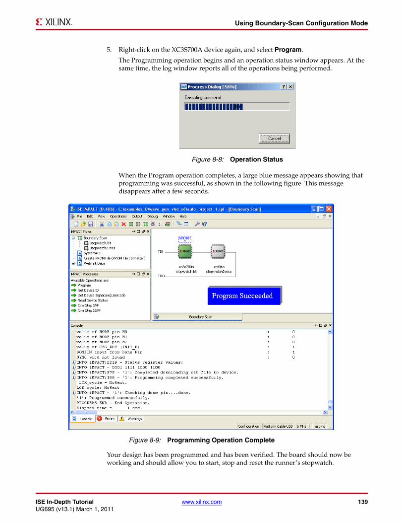
ISE In-Depth Tutorial www.xilinx.com 139UG695 (v13.1) March 1, 2011
Using Boundary-Scan Configuration Mode
5. Right-click on the XC3S700A device again, and select Program.
The Programming operation begins and an operation status window appears. At the same time, the log window reports all of the operations being performed.
When the Program operation completes, a large blue message appears showing that programming was successful, as shown in the following figure. This message disappears after a few seconds.
Your design has been programmed and has been verified. The board should now be working and should allow you to start, stop and reset the runner’s stopwatch.
X-Ref Target - Figure 8-8
Figure 8-8: Operation Status
X-Ref Target - Figure 8-9
Figure 8-9: Programming Operation Complete
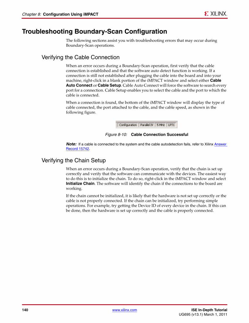
140 www.xilinx.com ISE In-Depth TutorialUG695 (v13.1) March 1, 2011
Chapter 8: Configuration Using iMPACT
Troubleshooting Boundary-Scan ConfigurationThe following sections assist you with troubleshooting errors that may occur during Boundary-Scan operations.
Verifying the Cable ConnectionWhen an error occurs during a Boundary-Scan operation, first verify that the cable connection is established and that the software auto detect function is working. If a connection is still not established after plugging the cable into the board and into your machine, right-click in a blank portion of the iMPACT window and select either Cable Auto Connect or Cable Setup. Cable Auto Connect will force the software to search every port for a connection. Cable Setup enables you to select the cable and the port to which the cable is connected.
When a connection is found, the bottom of the iMPACT window will display the type of cable connected, the port attached to the cable, and the cable speed, as shown in the following figure.
Note: If a cable is connected to the system and the cable autodetection fails, refer to Xilinx Answer Record 15742.
Verifying the Chain SetupWhen an error occurs during a Boundary-Scan operation, verify that the chain is set up correctly and verify that the software can communicate with the devices. The easiest way to do this is to initialize the chain. To do so, right-click in the iMPACT window and select Initialize Chain. The software will identify the chain if the connections to the board are working.
If the chain cannot be initialized, it is likely that the hardware is not set up correctly or the cable is not properly connected. If the chain can be initialized, try performing simple operations. For example, try getting the Device ID of every device in the chain. If this can be done, then the hardware is set up correctly and the cable is properly connected.
X-Ref Target - Figure 8-10
Figure 8-10: Cable Connection Successful
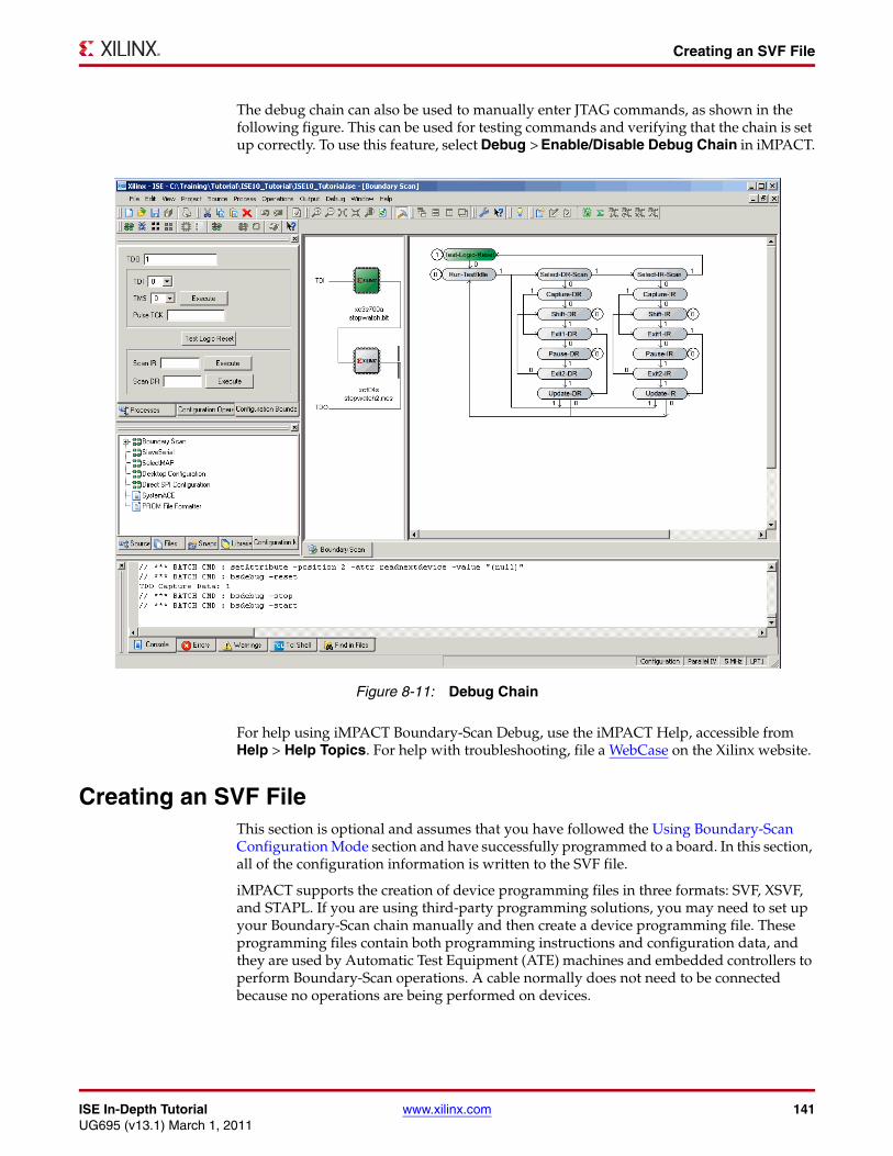
ISE In-Depth Tutorial www.xilinx.com 141UG695 (v13.1) March 1, 2011
Creating an SVF File
The debug chain can also be used to manually enter JTAG commands, as shown in the following figure. This can be used for testing commands and verifying that the chain is set up correctly. To use this feature, select Debug > Enable/Disable Debug Chain in iMPACT.
For help using iMPACT Boundary-Scan Debug, use the iMPACT Help, accessible from Help > Help Topics. For help with troubleshooting, file a WebCase on the Xilinx website.
Creating an SVF FileThis section is optional and assumes that you have followed the Using Boundary-Scan Configuration Mode section and have successfully programmed to a board. In this section, all of the configuration information is written to the SVF file.
iMPACT supports the creation of device programming files in three formats: SVF, XSVF, and STAPL. If you are using third-party programming solutions, you may need to set up your Boundary-Scan chain manually and then create a device programming file. These programming files contain both programming instructions and configuration data, and they are used by Automatic Test Equipment (ATE) machines and embedded controllers to perform Boundary-Scan operations. A cable normally does not need to be connected because no operations are being performed on devices.
X-Ref Target - Figure 8-11
Figure 8-11: Debug Chain
142 www.xilinx.com ISE In-Depth TutorialUG695 (v13.1) March 1, 2011
Chapter 8: Configuration Using iMPACT
Setting Up the Boundary-Scan ChainThis section assumes that you are continuing from the previous sections of this chapter and already have the chain detected. If not, skip to Manually Setting Up the JTAG Chain for SVF Generation to define the chain manually.
Setting Up the JTAG Chain for SVF Generation
To set up the JTAG chain, do the following:
1. Select Output > SVF File > Create SVF File to indicate that you are creating a programming file.
2. In the Create New SVF File dialog box, enter getid in the File Name field, and click Save.
3. An informational message appears stating that all device operations will be directed to the .svf file. Click OK.
Manually Setting Up the JTAG Chain for SVF Generation
For this tutorial, you may skip this section if you completed the Using Boundary-Scan Configuration Mode section.
The Boundary-Scan chain can be manually created or modified as well. To do this, do the following:
1. Ensure that you are in Boundary-Scan Mode by clicking the Boundary-Scan tab.
You can now add one device at a time.
2. Right-click on an empty space in the iMPACT Boundary-Scan window, and select Add Xilinx Device or Add Non-Xilinx device.
An Add Device dialog box opens, allowing you to select a configuration file.
3. Select stopwatch.bit, and then click Open.
The device is added where the large cursor is positioned. To add a device between existing devices, click on the line between them and then add the new device.
Repeat steps 2 and 3 to add the stopwatch.mcs file to the chain.
Note: The Boundary-Scan chain that you manually create in the software must match the chain on the board, even if you intend to program only some of the devices. All devices must be represented in the iMPACT window.
Writing to the SVF FileThe process of writing to an SVF file is identical to performing Boundary-Scan operations with a cable. You simply right-click on a device and select an operation. Any number of operations can be written to an SVF file.
In this section, you will be writing the device ID to the programming file for the first device, and performing further instructions for the second device.
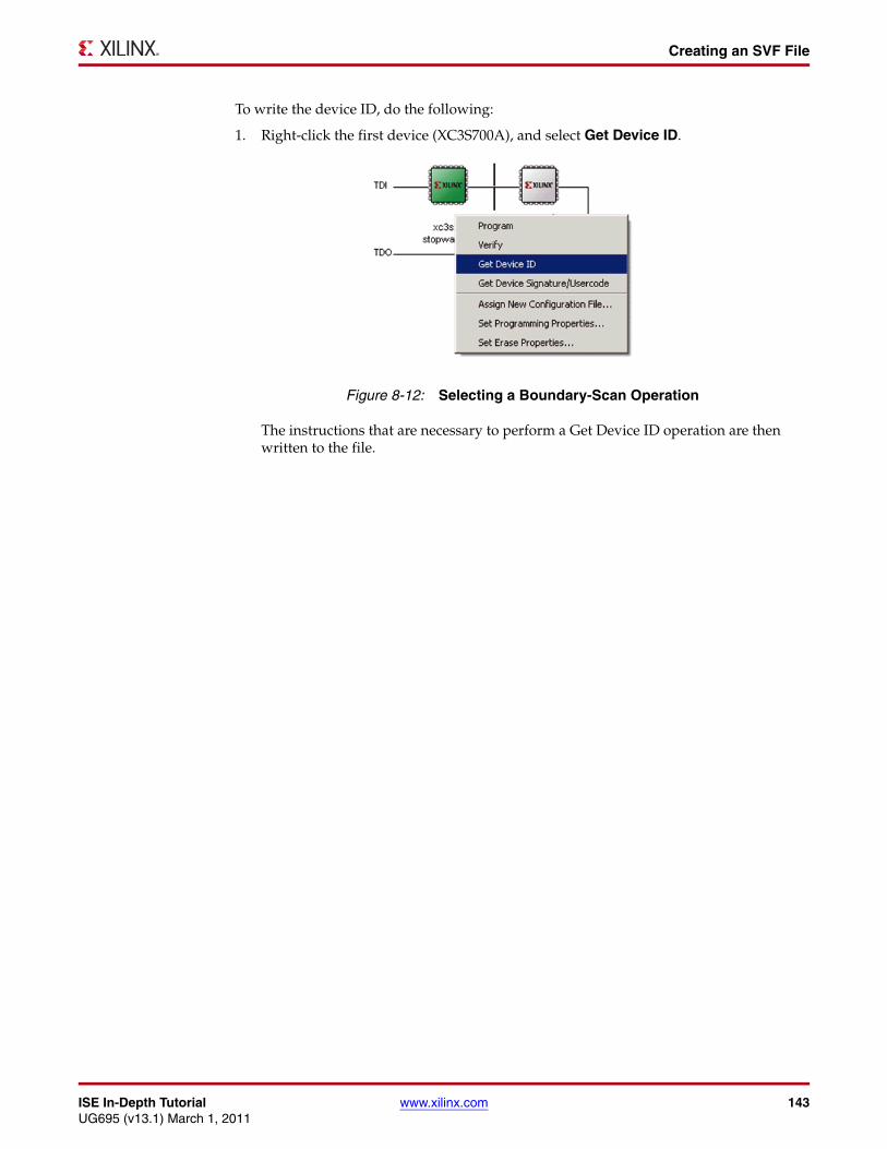
ISE In-Depth Tutorial www.xilinx.com 143UG695 (v13.1) March 1, 2011
Creating an SVF File
To write the device ID, do the following:
1. Right-click the first device (XC3S700A), and select Get Device ID.
The instructions that are necessary to perform a Get Device ID operation are then written to the file.
X-Ref Target - Figure 8-12
Figure 8-12: Selecting a Boundary-Scan Operation
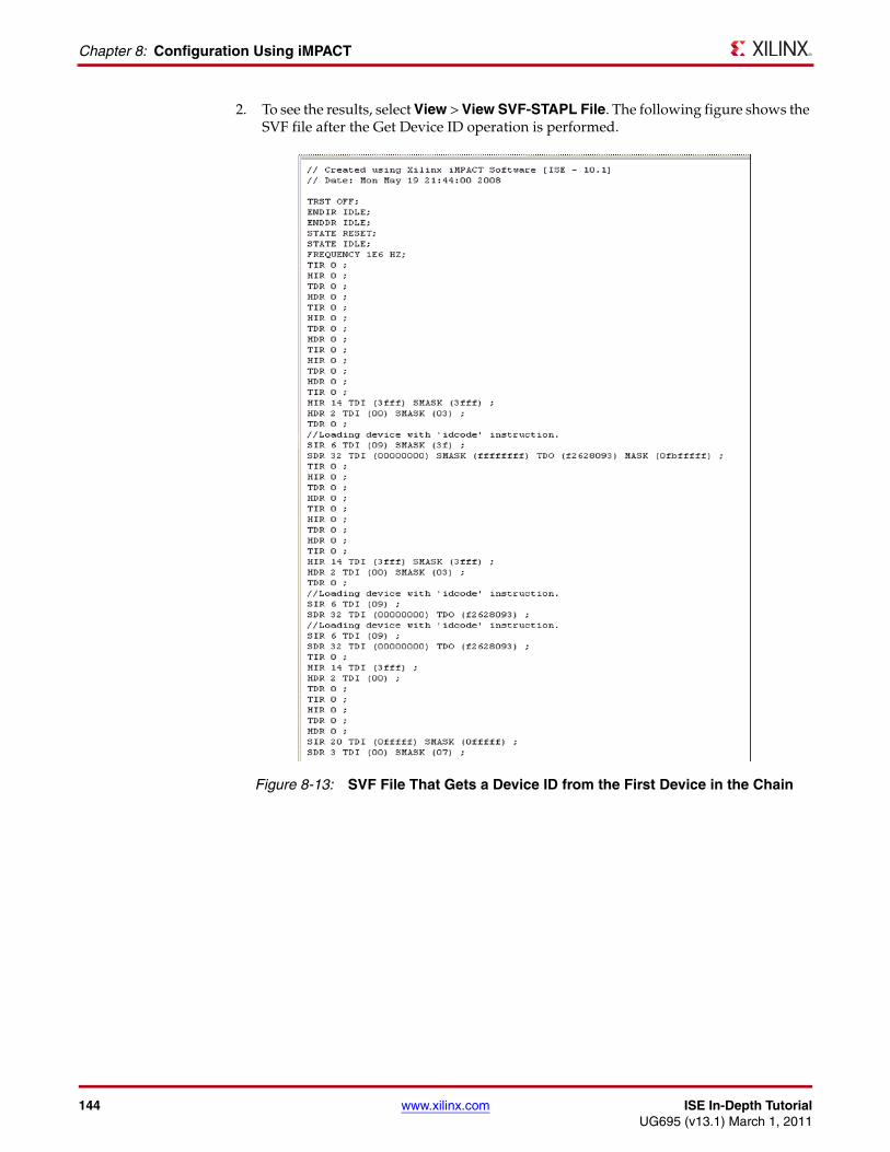
144 www.xilinx.com ISE In-Depth TutorialUG695 (v13.1) March 1, 2011
Chapter 8: Configuration Using iMPACT
2. To see the results, select View > View SVF-STAPL File. The following figure shows the SVF file after the Get Device ID operation is performed.
X-Ref Target - Figure 8-13
Figure 8-13: SVF File That Gets a Device ID from the First Device in the Chain
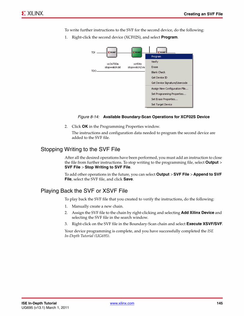
ISE In-Depth Tutorial www.xilinx.com 145UG695 (v13.1) March 1, 2011
Creating an SVF File
To write further instructions to the SVF for the second device, do the following:
1. Right-click the second device (XCF02S), and select Program.
2. Click OK in the Programming Properties window.
The instructions and configuration data needed to program the second device are added to the SVF file.
Stopping Writing to the SVF FileAfter all the desired operations have been performed, you must add an instruction to close the file from further instructions. To stop writing to the programming file, select Output > SVF File > Stop Writing to SVF File.
To add other operations in the future, you can select Output > SVF File > Append to SVF File, select the SVF file, and click Save.
Playing Back the SVF or XSVF FileTo play back the SVF file that you created to verify the instructions, do the following:
1. Manually create a new chain.
2. Assign the SVF file to the chain by right-clicking and selecting Add Xilinx Device and selecting the SVF file in the search window.
3. Right-click on the SVF file in the Boundary-Scan chain and select Execute XSVF/SVF.
Your device programming is complete, and you have successfully completed the ISE In-Depth Tutorial (UG695).
X-Ref Target - Figure 8-14
Figure 8-14: Available Boundary-Scan Operations for XCF02S Device

146 www.xilinx.com ISE In-Depth TutorialUG695 (v13.1) March 1, 2011
Chapter 8: Configuration Using iMPACT

ISE In-Depth Tutorial www.xilinx.com 147UG695 (v13.1) March 1, 2011
Appendix A
Additional Resources
Xilinx Resources• ISE Design Suite: Installation and Licensing Guide (UG798):
http://www.xilinx.com/support/documentation/sw_manuals/xilinx13_1/iil.pdf
• ISE Design Suite 13: Release Notes Guide (UG631): http://www.xilinx.com/support/documentation/sw_manuals/xilinx13_1/irn.pdf
• Xilinx® Documentation: http://www.xilinx.com/support/documentation
• Xilinx Global Glossary: http://www.xilinx.com/support/documentation/sw_manuals/glossary.pdf
• Xilinx Support: http://www.xilinx.com/support
ISE Documentation• ISE Documents:
http://www.xilinx.com/support/documentation/dt_ise13-1.htm
- Command Line Tools User Guide (UG628): http://www.xilinx.com/support/documentation/sw_manuals/xilinx13_1/devref.pdf
- Xilinx Synthesis and Simulation Design Guide (UG626): http://www.xilinx.com/support/documentation/sw_manuals/xilinx13_1/sim.pdf
- XST User Guide for Virtex-4, Virtex-5, Spartan-3, and Newer CPLD Devices (UG627): http://www.xilinx.com/support/documentation/sw_manuals/xilinx13_1/xst.pdf
- XST User Guide for Virtex-6, Spartan-6, and 7 Series Devices (UG687): http://www.xilinx.com/support/documentation/sw_manuals/xilinx13_1/xst_v6s6.pdf

148 www.xilinx.com ISE In-Depth TutorialUG695 (v13.1) March 1, 2011
Appendix A: Additional Resources