
Xiang Yi ,HangLiu,JiaFuLin , Student Member, IEEE IEEE ... 57.9-to-68.3 GHz 24.6 mW... · divider,...
26
IEEE Proof Web Version IEEE JOURNAL OF SOLID-STATE CIRCUITS, VOL. 49, NO. 2, FEBRUARY 2014 1 A 57.9-to-68.3 GHz 24.6 mW Frequency Synthesizer With In-Phase Injection-Coupled QVCO in 65 nm CMOS Technology Xiang Yi, Member, IEEE, Chirn Chye Boon, Senior Member, IEEE, Hang Liu, Jia Fu Lin, Student Member, IEEE, and Wei Meng Lim Abstract—A fully integrated 60 GHz frequency synthesizer with an in-phase injection-coupled quadrature voltage-controlled oscillator (IPIC-QVCO) is proposed. Through a particular sym- metrical coupling network formed by diode-connected transistors, the in-phase coupling is realized in the IPIC-QVCO, which re- duces both phase noise and phase error. A compact inductor-less divider chain is designed to reduce power consumption. A self-cor- recting low spur charge pump is employed to reduce reference spur. A standalone 60 GHz IPIC-QVCO and a fully integrated PLL are implemented in standard 65 nm low power CMOS technology. The measurement results show that the QVCO covers a frequency range from 57.88 to 68.33 GHz while consuming 11.4 mW power from a 1.2 V supply. The phase noise of the QVCO is –92 ~ –95 dBc/Hz at 1 MHz offset. The FOM and FOM T of the QVCO are –178.1 ~ –179.7 and –182.5 ~ –184.1 dBc/Hz respectively. The tuning range of the frequency synthesizer is from 57.9 to 68.3 GHz, and the power consumption is 24.6 mW. The phase noise of the frequency synthesizer is –89.8 ~ –91.5 dBc/Hz at 1 MHz offset across the frequency band. Index Terms—CMOS, frequency synthesizer, in-phase injec- tion-coupled (IPIC), low phase error, low phase noise, low power, millimeter-wave, PLL, quadrature voltage-controlled oscillator (QVCO), 60 GHz. I. INTRODUCTION N EXT-GENERATION short range high data rate wireless communication in the unlicensed 60 GHz frequency band was intensively investigated in the last decade. As defined in the 60 GHz standards, such as IEEE 802.15.3c, IEEE 802.11ad, WiGig, WirelessHD, and ECMA-387 [1]–[5], the total 9 GHz (57–66 GHz) bandwidth is divided into four 2.16 GHz channels. To achieve a higher data rate, complex modulations such as 16-QAM must be adopted, which increases the requirements of local oscillator’s (LO’s) phase noise and phase error. In recent years, it has already been demonstrated that advanced CMOS technology has the capability of realizing millimeter-wave (mm-wave) integrated circuits. CMOS implementation can Manuscript received July 10, 2013; revised October 14, 2013; accepted November 21, 2013. This paper was approved by Associate Editor Hossein Hashemi. This work was supported by the National Research Foundation Singapore through the Singapore MIT Alliance for Research and Technology’s Low Energy Electronic Systems research programme. The authors are with the School of Electrical and Electronic Engineering, Nanyang Technological University, Singapore 639798 (e-mail: YiXiang@ntu. edu.sg). Color versions of one or more of the figures in this paper are available online at http://ieeexplore.ieee.org. Digital Object Identifier 10.1109/JSSC.2013.2293021 reduce cost and improve yield, since RF front-end can be integrated with analog and digital baseband circuits. Direct-conversion architecture is popular for 60 GHz trans- ceivers because of its simple structure and fewer components [6]–[12]. Phase locked-loop (PLL) is an important block in a transceiver. Design of the wide range, low phase noise, low phase error and low power CMOS PLL for the 60 GHz direct-conversion transceiver is challenging, due to trade-offs between tuning range, phase noise, phase error, and power con- sumption. There are many methods for generating mm-wave quadrature LO signals, but they suffer from many problems. 1) The most common method is through a conventional mm-wave parallel quadrature voltage-controlled oscillator (P-QVCO), but its phase noise is poor [13]. 2) The method of using a divide-by-2 divider after a VCO with double LO fre- quency prevails in multi-GHz applications, but it is difficult to design a VCO and a divider at very high frequency. Moreover, the power consumption of this method is high. 3) If passive components such as an RC polyphase filter or quadrature hybrid coupler are used to produce quadrature signals, we usually need buffers to compensate their loss, so the power consumption is also high [6]. 4) Using an injection-locked multiplier is a good choice [14], but the disadvantages are limited locking range and intrinsic phase error due to the imbalance of the structure, or quadrature inputs are needed to overcome these two drawbacks [9]. In this work, we present a wide range, low phase noise, and low power 60 GHz quadrature PLL [15]. The simplified block diagram of the proposed PLL is shown in Fig. 1. It is an integer- third-order charge-pump PLL with a 135 MHz reference input. The 60 GHz in-phase injection-coupled (IPIC) QVCO is proposed to reduce phase noise and phase error. Its operation frequency can cover the four required frequency spots in IEEE 802.15.3c and other compatible 60 GHz standards. The low power inductor-less frequency divider chain consists of a modified divide-by-4 dynamic current-mode logic (DCML) divider, a divide-by-4 multi-phase injection-locked frequency divider (ILFD), and a multi-modulus true-single-phase-clock (TSPC) divider. The low spur self-correcting charge pump is employed to reduce the reference spur. A standalone 60 GHz IPIC-QVCO and a fully integrated 60 GHz PLL are imple- mented in standard 65 nm low power CMOS technology to demonstrate our ideas. Measurement results show that the proposed IPIC-QVCO and quadrature PLL can achieve good performance with low power consumption. 0018-9200 © 2013 IEEE
Transcript of Xiang Yi ,HangLiu,JiaFuLin , Student Member, IEEE IEEE ... 57.9-to-68.3 GHz 24.6 mW... · divider,...
IEEE
Pro
of
Web
Ver
sion
IEEE JOURNAL OF SOLID-STATE CIRCUITS, VOL. 49, NO. 2, FEBRUARY 2014 1
A 57.9-to-68.3 GHz 24.6 mW Frequency SynthesizerWith In-Phase Injection-Coupled QVCO in
65 nm CMOS TechnologyXiang Yi, Member, IEEE, Chirn Chye Boon, Senior Member, IEEE, Hang Liu, Jia Fu Lin, Student Member, IEEE,
and Wei Meng Lim
Abstract—A fully integrated 60 GHz frequency synthesizerwith an in-phase injection-coupled quadrature voltage-controlledoscillator (IPIC-QVCO) is proposed. Through a particular sym-metrical coupling network formed by diode-connected transistors,the in-phase coupling is realized in the IPIC-QVCO, which re-duces both phase noise and phase error. A compact inductor-lessdivider chain is designed to reduce power consumption. A self-cor-recting low spur charge pump is employed to reduce referencespur. A standalone 60 GHz IPIC-QVCO and a fully integratedPLL are implemented in standard 65 nm low power CMOStechnology. The measurement results show that the QVCO coversa frequency range from 57.88 to 68.33 GHz while consuming11.4 mW power from a 1.2 V supply. The phase noise of theQVCO is –92 ~ –95 dBc/Hz at 1 MHz offset. The FOM and FOMTof the QVCO are –178.1 ~ –179.7 and –182.5 ~ –184.1 dBc/Hzrespectively. The tuning range of the frequency synthesizer is from57.9 to 68.3 GHz, and the power consumption is 24.6 mW. Thephase noise of the frequency synthesizer is –89.8 ~ –91.5 dBc/Hzat 1 MHz offset across the frequency band.
Index Terms—CMOS, frequency synthesizer, in-phase injec-tion-coupled (IPIC), low phase error, low phase noise, low power,millimeter-wave, PLL, quadrature voltage-controlled oscillator(QVCO), 60 GHz.
I. INTRODUCTION
N EXT-GENERATION short range high data rate wirelesscommunication in the unlicensed 60 GHz frequency band
was intensively investigated in the last decade. As defined inthe 60 GHz standards, such as IEEE 802.15.3c, IEEE 802.11ad,WiGig, WirelessHD, and ECMA-387 [1]–[5], the total 9 GHz(57–66 GHz) bandwidth is divided into four 2.16 GHz channels.To achieve a higher data rate, complex modulations such as16-QAM must be adopted, which increases the requirements oflocal oscillator’s (LO’s) phase noise and phase error. In recentyears, it has already been demonstrated that advanced CMOStechnology has the capability of realizing millimeter-wave(mm-wave) integrated circuits. CMOS implementation can
Manuscript received July 10, 2013; revised October 14, 2013; acceptedNovember 21, 2013. This paper was approved by Associate Editor HosseinHashemi. This work was supported by the National Research FoundationSingapore through the Singapore MIT Alliance for Research and Technology’sLow Energy Electronic Systems research programme.
The authors are with the School of Electrical and Electronic Engineering,Nanyang Technological University, Singapore 639798 (e-mail: [email protected]).
Color versions of one or more of the figures in this paper are available onlineat http://ieeexplore.ieee.org.
Digital Object Identifier 10.1109/JSSC.2013.2293021
reduce cost and improve yield, since RF front-end can beintegrated with analog and digital baseband circuits.
Direct-conversion architecture is popular for 60 GHz trans-ceivers because of its simple structure and fewer components[6]–[12]. Phase locked-loop (PLL) is an important block ina transceiver. Design of the wide range, low phase noise,low phase error and low power CMOS PLL for the 60 GHzdirect-conversion transceiver is challenging, due to trade-offsbetween tuning range, phase noise, phase error, and power con-sumption. There are many methods for generating mm-wavequadrature LO signals, but they suffer from many problems.1) The most common method is through a conventionalmm-wave parallel quadrature voltage-controlled oscillator(P-QVCO), but its phase noise is poor [13]. 2) The method ofusing a divide-by-2 divider after a VCO with double LO fre-quency prevails in multi-GHz applications, but it is difficult todesign a VCO and a divider at very high frequency. Moreover,the power consumption of this method is high. 3) If passivecomponents such as an RC polyphase filter or quadrature hybridcoupler are used to produce quadrature signals, we usually needbuffers to compensate their loss, so the power consumptionis also high [6]. 4) Using an injection-locked multiplier is agood choice [14], but the disadvantages are limited lockingrange and intrinsic phase error due to the imbalance of thestructure, or quadrature inputs are needed to overcome thesetwo drawbacks [9].
In this work, we present a wide range, low phase noise,and low power 60 GHz quadrature PLL [15]. The simplifiedblock diagram of the proposed PLL is shown in Fig. 1. It isan integer- third-order charge-pump PLL with a 135 MHzreference input. The 60 GHz in-phase injection-coupled (IPIC)QVCO is proposed to reduce phase noise and phase error. Itsoperation frequency can cover the four required frequency spotsin IEEE 802.15.3c and other compatible 60 GHz standards. Thelow power inductor-less frequency divider chain consists ofa modified divide-by-4 dynamic current-mode logic (DCML)divider, a divide-by-4 multi-phase injection-locked frequencydivider (ILFD), and a multi-modulus true-single-phase-clock(TSPC) divider. The low spur self-correcting charge pump isemployed to reduce the reference spur. A standalone 60 GHzIPIC-QVCO and a fully integrated 60 GHz PLL are imple-mented in standard 65 nm low power CMOS technology todemonstrate our ideas. Measurement results show that theproposed IPIC-QVCO and quadrature PLL can achieve goodperformance with low power consumption.
0018-9200 © 2013 IEEE

IEEE
Pro
of
Web
Ver
sion
2 IEEE JOURNAL OF SOLID-STATE CIRCUITS, VOL. 49, NO. 2, FEBRUARY 2014
Fig. 1. Simplified PLL block diagram.
The paper is organized as follows. Section II discusses theproposed IPIC-QVCO, including architecture, analysis, and cir-cuit design. Section III describes the frequency divider chainand charge pump design. Experimental results are provided inSection IV and conclusions are drawn in Section V.
II. IN-PHASE INJECTION-COUPLED QVCO
A. Proposed In-Phase Injection-Coupled QVCO
In general, the QVCO consists of two identical oscillatorspulling each other, through coupling networks, to lock at acommon frequency with quadrature phase. It is well knownthat in QVCO, the in-phase coupling can reduce both phasenoise and phase error [16]. Many phase shifting techniqueswere presented to realize the in-phase coupling [16]–[21]. Buttheir coupling networks are either RC-based or LC-based phaseshifters, which are both frequency-dependent.
The in-phase coupling is realized in the proposedIPIC-QVCO by using the frequency-independent network,instead of the frequency-dependent phase shifter. In fact, themost neglected thing is that, quadrature signals always exist in aQVCO inherently. Therefore, intuitively, in-phase coupling canbe realized through a particular symmetrical coupling network.Similar concepts have already been demonstrated in multiphaseinjection ILFDs [22]–[24]. We will prove that this concept alsoworks in our QVCO. The schematic of the proposed QVCO isshown in Fig. 2. The two identical differential LC cross-coupledVCOs are coupled through a symmetrical coupling network. Inthe coupling network, each diode-connected transistor connectstwo oscillation nodes with phase difference, e.g., transistor
connects node and node . So the four diode-con-nected transistors form a symmetrical ring. As will be analyzedlater, this configuration can generate in-phase injection currentwith the tank current.
To understand the basic concept of the in-phase coupling, wewill now describe the operation of the IPIC-QVCO. Let us as-sume that the tank is high enough that only the fundamentalcomponents need to be considered. When the QVCO is oper-ating, ’s gate voltage has a phase of 0, and the sourcevoltage has a phase of , as shown in Fig. 3(a). Since theamplitudes of and are the same, the gate-source voltage
has a phase of . Therefore, the phase of ’s drain cur-rent is also . is turned on only when is largerthan its threshold voltage . The conduction angle is less than
, so works in Class-C mode.Similarly, the phase of ’s drain current is . The
current , injected into the node from the coupling net-work, is equal to , as shown in Fig. 3(b). Thus, is
Fig. 2. Schematic of the proposed IPIC-QVCO.
Fig. 3. Analysis of (a) diode-connected transistor and (b) coupling network inIPIC-QVCO.
shifted by exactly compared with or . A similar situa-tion exists in the other three nodes , , and . There-fore, the in-phase coupling is realized in IPIC-QVCO. Since thecoupling network does not employ any passive component, it isfrequency-independent. As will be demonstrated in simulationand measurement, the parasitic capacitance has little impact onthe in-phase coupling even at the mm-wave frequency.
Previous analysis assumed that the phase difference betweenand is . What happens if this phase difference is? The same analysis reveals that, in this case, is per-
pendicular to , which is similar to that in the P-QVCO. Laterwe will prove that the second case does not exist in IPIC-QVCO.Therefore, output quadrature phases are in a known sequencethat is essential for most transceivers.

IEEE
Pro
of
Web
Ver
sion
YI et al.: A 57.9-TO-68.3 GHz 24.6 mW FREQUENCY SYNTHESIZER WITH IN-PHASE INJECTION-COUPLED QVCO IN 65 nm CMOS TECHNOLOGY 3
Fig. 4. Models of (a) diode-connected transistor, half of cross-coupled regenerative pair, and (b) IPIC-QVCO. (c) Magnitude and phase of tank impedance.
B. Analysis of Oscillation Mode, Phase Error, and PhaseNoise
In this subsection, we will analyze the properties of IPIC-QVCO, including oscillation mode, stability, phase error, andphase noise, based on Adler’s equation.
We start with the drain current of a diode-connected tran-sistor in the coupling network. Assuming that its and are
and respectively, where ,, is the oscillation amplitude, is the oscillation fre-
quency, and . Thus, the gate-source voltage is
(1)
The transistor is in saturation region when it is turned on. Dueto the velocity saturation in modern transistors, as presented inAppendix A, the amplitude of its drain current at fundamentalfrequency is given by
(2)
where , is the short-channel effect mod-eling parameter and is the saturation velocity of the tran-sistor. Thus, when , the amplitude of its drain current atfundamental frequency is .
In this case, the amplitude of the injection current shownin Fig. 3(b) is
(3)
According to the previous analysis, the diode-connectedtransistor can be modeled as a voltage-dependent transcon-ductor as depicted in Fig. 4(a). Let us suppose that thezero-crossings of the oscillation voltage commutate the tailcurrent . In the high- tank, only the fundamental com-ponent of the square-wave current needs to be taken intoaccount. Thus, half of the cross-coupled regenerative paircan be modeled as the hard-limiter transconductor with anoutput current of . The whole model of IPIC-QVCO isshown in Fig. 4(b). The resonant frequency and loss of the
tank are and respectively. Tank isequal to . We assume the four oscillation voltages inthe two oscillators are , , and
. Therefore, according to (1) and (2), we obtainthe drain currents of diode-connected transistors in the cou-pling network: ,
,, and
.The IPIC-QVCO can be treated as two strongly coupled os-
cillators. Thus, applying these expressions to the generalizedAdler’s equation in [16] leads to the differential equations (4)and (5) shown at the bottom of the page. We will mainly usethese two differential equations to analyze the IPIC-QVCO.
(4)
(5)
IEEE
Pro
of
Web
Ver
sion
4 IEEE JOURNAL OF SOLID-STATE CIRCUITS, VOL. 49, NO. 2, FEBRUARY 2014
1) Oscillation Mode and Stability: Let us suppose the twooscillators are stable and oscillate at a common frequency .Substituting and into (4) and (5), thesolutions of are ; see equation (6) at the bottom ofthe page, where is the coupling strength and defined as
(7)
From the analysis of the previous subsection, we know thatshould be less than , that is . The second
and third solutions are non-quadrature. The first solution indi-cates that the IPIC-QVCO has a phase difference of be-tween the two oscillators. Substituting into (4) and(5) gives . The result is obvious:the total injection current from the coupling network is inphase with the oscillating current . So there is no additionalphase-shift in the tank. The oscillator operates at the resonantfrequency of the tank as shown in Fig. 4(c). That is, theIPIC-QVCO is in-phase injection-coupled.
Perturbation analysis can be used to check the stability ofthis solution. A stable system should correct the perturbationby itself. We assume that the phases of the two oscillators havesome small change due to perturbation: and
, where . Substituting theseexpressions into (4) and (5) and simplifying the results, we get
(8)
where is the dampingtime-constant of the system. The larger coupling strength
leads to smaller and a faster system in suppressing thedisturbance. Since , any perturbation in the phase ofthe output voltage will decay, which means that this mode isunconditionally stable.
We can also apply perturbation analysis to check the stabilityof solutions . However, due to the complexity of the expres-sions, little information can be obtained from the expressionsdirectly. We have varied the parameters within the range of allpractical values for 60 GHz QVCO, and the quantitative anal-ysis shows that the two solutions are unstable. In addition, thesetwo solutions have not been observed in our simulation.
2) Phase Error due to Mismatches: In practical implemen-tation, there are device mismatches in QVCOs because of theasymmetric layout or the process variation, which leads to phaseerror. The mismatches may exist in the tank resonant fre-quency, tank quality factor, coupling network, and tail current.We suppose all the mismatches are in the second oscillator:oscillation frequency , tank quality factor
, dimension of transistors in the coupling net-work , of transistors in the
Fig. 5. Simulated (symbol) and calculated (solid line) phase errors due to mis-matches in coupling network and .
coupling network , and tail current, which results in the phase error represented by
. Let us assume the phase error is in the second oscillator, soits phase is . Substituting all these expres-sions into (4) and (5) and simplifying the results, we obtain
(9)
Similar to the P-QVCO, if the coupling strength increasesor tank decreases, the phase error of IPIC-QVCO due tomismatch decreases. Interestingly, also represents the sup-pression of phase error due to mismatch because a smallresults in a small phase error. Fig. 5 compares the real transistorsimulated and calculated phase errors due to mismatches in thecoupling network and . The oscillation frequency is set to60 GHz, with a tank of 6, tail current of 5 mA, and couplingstrength of 0.2. The theoretical results show good agreementwith the simulation results.
It is noteworthy that, as implied by (9), the quadrature accu-racy is not affected by mismatches of and , but by the mis-match in the coupling network. This seemingly contradictoryphenomenon can be explained with voltage and current phasordiagrams. Suppose the IPIC-QVCO has quadrature outputs inthe initial state with no mismatch. Mismatches of and willcause the amplitude of output voltages in the second oscillatorto change as depicted in Fig. 6(a). Although ( 1,2,3,4)and the corresponding are changed, is still in phasewith the output voltage and . Therefore, the QVCO re-mains locked to with quadrature output phases. On the otherhand, the mismatch in the coupling network will change and
(6)

IEEE
Pro
of
Web
Ver
sion
YI et al.: A 57.9-TO-68.3 GHz 24.6 mW FREQUENCY SYNTHESIZER WITH IN-PHASE INJECTION-COUPLED QVCO IN 65 nm CMOS TECHNOLOGY 5
Fig. 6. Voltage and current phasor diagrams due to (a) , , and (b) couplingnetwork mismatches.
, instead of , as shown in Fig. 6(b). Thus, has aphase-shift with . The different phase-shifts in the two os-cillators will cause their output phases to depart from quadra-ture, and thus phase error appears. Fortunately, since the cou-pling network is simple and symmetric, the mismatch causedby the layout is small. The phase error is less than 1 within a5% mismatch in the coupling network as depicted in Fig. 5.
3) Phase Noise: Phase noise can be analyzed as weak in-jection by using Alder’s equation. We treat white noise in eachdevice as individual weak injection current into the two oscilla-tors. The injection currents directly or indirectly lead to phasenoise. By following the steps in [16], the phase noise causedby the white noise in the tank, cross-coupled pair, and couplingnetwork can be derived from (4) and (5):
(10)
where is the Boltzmann constant, is the absolute tempera-ture, and is the MOS channel noise factor. The effective outputvoltage is . The factor represents the ratioof current flow into the coupling network. This is similar to theP-QVCO if we merge the tail current source in the cross-coupledpair and the coupling network, because a portion of is con-sumed by the coupling network. In contrast to the phase error,the phase noise of IPIC-QVCO due to white noise increases withcoupling strength and decreases with tank . Therefore, thereare trade-offs in coupling strength and tank when consideringboth phase error and phase noise in IPIC-QVCO design. Fig. 7compares the simulated phase noise and calculated phase noiseusing (10), and the difference is less than 1.5 dB.
Flicker noise in the cross-coupled pair of a differential LCoscillator contributes to negligible phase noise since it is sam-pled at twice the oscillation frequency [25]. However, flickernoise in the coupling network of P-QVCO introduces signifi-cant phase noise. This is because in the real circuit, the oscilla-tion frequency of P-QVCO depends on the transconductance ofthe coupling network . The flicker noise slowly modulates
and is up-converted into the close-in phase noise
Fig. 7. Simulated ( ) and calculated (solid line) phase noise from white noisein tank, cross-coupled pair, and coupling network.
[26]. In addition, the noise current injects at the zero-crossingof the output voltage, exacerbating the flicker noise up-conver-sion. In contrast to the P-QVCO, the oscillation frequency of theIPIC-QVCO is which is independent of the transistors, andthe coupling is in phase. Thus, the influence of flicker noise inthe coupling network of IPIC-QVCO is not so critical. This canbe verified through the impulse sensitivity function (ISF) sim-ulation [27]. NMF is the normalized instantaneous drain cur-rent in one oscillation cycle. Effective ISF is the product of ISFand NMF. It is obvious from the simulation that, compared withP-QVCO, IPIC-QVCO has much smaller DC value and rootmean square value of the effective ISF, resulting in less flickernoise up-conversion and lower phase noise.
Flicker noise in tail current source is another serious issue inP-QVCO. Analyzing IPIC-QVCO by using (4) and (5) givesthat flicker noise in tail current source does not contribute tophase noise directly. The flicker noise varies the amplitudeof the output voltage, and is converted into the close-inphase noise through a varactor. The difference of flicker noiseup-conversion between P-QVCO and IPIC-QVCO can bedemonstrated in simulation. The tail current sources in Fig. 2are implemented with NMOS current mirrors, and the sameconditions in Fig. 5 are adopted. Simulation results depictthat, the phase noise of IPIC-QVCO due to flicker noise in tailcurrent source is at least 3 dB lower than that of P-QVCO.Therefore, IPIC-QVCO also desensitizes flicker noise in tailcurrent source up-conversion.
C. 60 GHz IPIC-QVCO Design
Fig. 8 shows the full schematic of 60 GHz IPIC-QVCO. Thecoupling network without the gate bias voltage (i.e., formedby direct diode-connected transistors) is used in PLL, while thecoupling network with is used in a standalone QVCO to ex-plore the characteristics of the in-phase injection coupling.
A 3-bit binary-weight switch-capacitor bank is used fordiscrete tuning. The resistor-biased switch contributes to lessnoise than other conventional switches [28]. Metal-oxide-metal(MOM) capacitors are used for their small capacitance andconvenient layout. A small p-type varactor is used for con-tinuous tuning. represents the digitally controlled variableresistor in order to reduce flicker noise. The DC voltage of theoscillation nodes is set to about half of the supply voltage

IEEE
Pro
of
Web
Ver
sion
6 IEEE JOURNAL OF SOLID-STATE CIRCUITS, VOL. 49, NO. 2, FEBRUARY 2014
Fig. 8. Full schematic of the proposed 60 GHz IPIC-QVCO.
Fig. 9. Simulated phase noise and phase error versus (a) coupling factor and (b) bias voltage in 60 GHz IPIC-QVCO.
to fully utilize the tuning characteristic of the varactor. Theeight overlapped bands can cover the four required frequencyspots in IEEE 802.15.3c with low VCO gain ( ).
The passive devices such as inductors and transmission linesare all custom designed. Since the parasitics of interconnectsand devices play important roles in the mm-wave circuit design,we use an electromagnetic (EM) simulator to obtain their -pa-rameters. The -parameters files are then sent back to CadenceSpectreRF for circuit simulation with active devices. Becausethe of 65 nm transistors are sufficient high for 60 GHzapplication, the model described in the previous subsection isvalid as long as the tank or S-parameters files take the parasiticsof interconnects and devices into account.
As mentioned previously, there is a trade-off between phasenoise and phase error in terms of the coupling strength . Wecan choose a proper and power to meet the phase noise andphase error requirements simultaneously. However, to get a par-ticular is tedious for the mm-wave circuit design, because itis difficult to distinguish the currents flowing into the transistorsand their parasitics. A more efficient method for mm-wave cir-cuit design is through simulation iterations. We define the cou-pling factor as the ratio of the transistor’s width in the cou-
pling network to the transistor’s width in the cross-coupled re-generative pair. Note that in IPIC-QVCO, is determined bythe coupling factor and the bias voltage . Simulations arecarried out to find the optimum values of and . We choose
GHz, m m, pH, ,mA. Fig. 9 shows the simulated phase noise and phase
error by varying and . We note that the phase error is smalland does not change much if and V. So thecoupling network without , which is used in our QPLL, canachieve good performance. In our design, to ensure the start-upand the wide tuning range under the process and temperaturevariation, a small coupling network is chosen. is set to20 m, and is chosen as 1/3.
We also compare IPIC-QVCO with other conventionalQVCOs: P-QVCO, bottom series QVCO [29], superhar-monic-coupled QVCO [30], and magnetically-coupled QVCO[17]. Unless otherwise stated, all the conditions are the same.The simulated performances are summarized in Table I. Com-pared with other conventional QVCOs, the IPIC-QVCO haslarge output amplitude, good phase noise, and good phaseerror. Moreover, the IPIC-QVCO exhibits good performance atmulti-GHz frequencies in our simulation.

IEEE
Pro
of
Web
Ver
sion
YI et al.: A 57.9-TO-68.3 GHz 24.6 mW FREQUENCY SYNTHESIZER WITH IN-PHASE INJECTION-COUPLED QVCO IN 65 nm CMOS TECHNOLOGY 7
TABLE ISIMULATED PERFORMANCES OF 60 GHZ IPIC-QVCO AND OTHER CONVENTIONAL QVCOS
Fig. 10. (a) Schematic, (b) simulated locking range and (c) waveforms of the modified DCML divide-by-4 divider.
III. DIVIDER CHAIN AND CHARGE PUMP DESIGN
A. Low Power Inductor-Less Divider Chain
Designing frequency dividers is challenging in mm-wavePLL since they may consume substantial power. Large areais another issue due to the use of inductors. In this work, theinductor-less DCML divider, ILFD, and TSPC divider areimplemented in cascade. By using these divider topologies, thelow power and small area can be achieved simultaneously. Wewill describe them separately.
Fig. 10(a) depicts the schematic of the modified DCML di-vide-by-4 frequency divider. Compared with a traditional CMLdivider, the DCML divider uses the parasitic capacitor in dif-ferential amplifier pair, instead of a static cross-coupled latch,to store the data [21]. By removing the cross-coupled pairs,the maximum operation frequency of the divider is increased,making it suitable for mm-wave frequency. To further improveits performance, two methods have been adopted. Firstly, lowthreshold voltage (low- ) devices are used to increase the max-imum operation frequency for their higher . Secondly, wemerge the switches of the same input clock of the DCML di-vider in [21], i.e., node and node are connected together.
By connecting and , we now present a balanced andhigh conductance point at the input frequency. Therefore, theinjection currents of the modified DCML divider are larger thanthat of the conventional DCML divider, as shown in Fig. 10(c).From the point of view of injection locking, the locked band-width of the modified DCML divider is enlarged. In order tobalance the output loadings, all the eight-phase outputs of theDCML divider serve as the inputs of the next divider. Fig. 10(b)shows its post-layout simulation results with different bias volt-ages . With about 300 mV peak-to-peak input voltage, thedivider works from 35 GHz to 77 GHz, with at least 3 GHzbandwidth in each sub-band. Thus, two sub-bands can cover thefour frequency spots of IEEE 802.15.3c. The simulated powerconsumption is about 9.0 mW at 60 GHz frequency, at a 1.2 Vsupply.
Fig. 11(a) depicts the schematic of the injection-locked di-vide-by-4 divider. Its eight-phase inputs are from the outputs ofthe DCML divider. Each two adjacent phase inputs are addedthrough transistors to generate four injection currents. The fourinjection currents are in quadrature with enhanced amplitude asshown in Fig. 11(b). The multiphase injection with proper se-quence can improve the locking range of the divide-by-4 ILFD

IEEE
Pro
of
Web
Ver
sion
8 IEEE JOURNAL OF SOLID-STATE CIRCUITS, VOL. 49, NO. 2, FEBRUARY 2014
Fig. 11. (a) Schematic, (b) phasor of injection current, and (c) simulated locking range of the injection-locked divide-by-4 divider.
[31]. Fig. 11(c) shows its post-layout simulation results withdifferent bias voltages . With about 300 mV peak-to-peakinput voltage, the divider works from 8 GHz to 28 GHz. Thelocking range of each sub-band is large enough to cover about5 GHz input range. The simulated power consumption is lessthan 3.2 mW with a 1.2 V supply.
The multi-modulus divider consists of four divide-by-2/3TSPC divider cells and one control circuit. It can realize thefour-division modulus (27, 28, 29, and 30) with low powerconsumption. The output of the multi-modulus divider is takenfrom the first divide-by-2/3 divider to reduce the phase noise,because it is retimed by the high frequency input. The simulatedpower consumption is about 0.7 mW.
B. Low Spur Charge Pump
The programmable self-correcting low spur CP, shownin Fig. 12(a), is modified from [32]. The voltage-to-current(VI) converter, which includes a rail-to-rail amplifier, sensesthe voltage difference between and , and corrects themismatch between charge and discharge currents. Thus, thestatic phase offset is minimized and the effective tuning rangis maximized. However, there are two problems in [32]: clockfeedthrough and charge injection in the switches. In our pro-posed charge pump, two measures are taken to avoid these twoproblems and further reduce spurious level. First, the UP/DNswitches are moved to the source of current source transistors toeliminate the clock feedthrough and charge injection. Second,the VCO control voltage is connected to , instead of .So can be regarded as after a unity-gain amplifier. Thebenefit is that the ripple in caused by the reference clock canbe filtered by this follower as long as its bandwidth is lessthan the reference frequency . It also isolates the switchesand , so the clock has negligible effect on the output. On
the other hand, is designed to be significantly larger thanthe PLL loop bandwidth , to minimize the effect onthe system loop characteristics and stability. In this design,
can be programmed from 0.5 to 2 MHz, and andare about 40 and 135 MHz, respectively. Fig. 12(b) depicts
the simulated waveforms of when it is connected to andrespectively. As expected, the amplifier does not interfere
with the locking process. The ripple of connected to ismuch smaller, and is reduced by about 10 times compared withthat connected to . We also performed a transient simulationto observe the reference spur levels with non-idealities: 10%charge/discharge current mismatch and 1 leakage currentin the LPF as shown in Fig. 12(c). When is connected to
, the reference spur is consistently reduced by about 10 dBcompared with when is connected to . The simulatedpower consumption of this charge pump is about 0.3 mW.
IV. EXPERIMENTAL RESULTS
A 60 GHz standalone IPIC-QVCO and a 60 GHz PLL areimplemented in GLOBALFOUNDRIES standard 65 nm lowpower CMOS technology. Fig. 13 shows the die micrographof the standalone QVCO and the complete PLL, which occupy0.26 0.15 mm and 0.32 0.60 mm , respectively.
The standalone IPIC-QVCO consumes 11.4 mW (not in-cluding output buffers) from a 1.2 V supply. The measuredVCO tuning curves are shown in Fig. 14. The eight bands ofthe QVCO cover a frequency range of 57.88 to 68.33 GHz, i.e.,16.6% around the center frequency, with a tuning sensitivityless than 2 GHz/V. As depicted in Fig. 15, the measuredQVCO phase noises for a 62.66 GHz carrier are 94.2 and
115.0 dBc/Hz at 1 and 10 MHz offset, respectively. Thecorner frequency between the and region is less

IEEE
Pro
of
Web
Ver
sion
YI et al.: A 57.9-TO-68.3 GHz 24.6 mW FREQUENCY SYNTHESIZER WITH IN-PHASE INJECTION-COUPLED QVCO IN 65 nm CMOS TECHNOLOGY 9
Fig. 12. (a) Schematic and (b) simulated output voltages of the proposed charge pump. [Please include a subcaption for part (c).]
Fig. 13. Die photographs of the standalone IPIC-QVCO and the complete PLL.
than 2 MHz, demonstrating a low flicker noise up-conver-sion. Note that the corner frequency can be further reducedif the size of the diode-connected transistors in the couplingnetwork is larger. We also measured the phase noise perfor-mance across the tuning range from six samples. The phasenoise is between 92 and 95 dBc/Hz at 1 MHz offset. TheFigure of Merit (FOM) and FOM are 178.1 179.7 and
182.5 184.1 dBc/Hz at 1 MHz offset, respectively. Thephase and amplitude errors are measured by down-convertingthe quadrature signals to about 250 MHz. Fig. 17 shows that thephase error is less than 0.7 and the amplitude error is less than0.9 dB across 6 samples for at 0.6 V. To verify the charac-teristics of the in-phase coupling, we measure the IPIC-QVCOby varying the bias voltage , as depicted in Fig. 18. Mea-surement results show that the frequency is almost constantwhen increases, indicating the coupling is in phase. Thephase noise increases and the phase error decreases while thecoupling strength becomes stronger, which coincides with theanalysis results. Table II shows the summarized measurementresults and a comparison with other state-of-the-art 60 GHzCMOS QVCOs. The proposed IPIC-QVCO has good phasenoise and small phase error, and consumes the least power.
The PLL consumes 24.6 mW (not including open-drainoutput buffers) from a 1.2 V supply, of which, about 11.4, 12.7,and 0.5 mW are consumed by QVCO, divider chain and otherblocks, respectively. The operation range of the PLL is from57.9 to 68.3 GHz. When the reference input 135 MHz,the PLL can be locked to the four frequencies defined by theIEEE 802.15.3c standard: 58.32, 60.48, 62.64, and 64.80 GHz.As shown in Fig. 19, PLL phase noise is 91.0 dBc/Hz at1 MHz offset from a 62.64 GHz carrier. Phase noise con-tributors are also plotted in Fig. 19 through a combination

IEEE
Pro
of
Web
Ver
sion
10 IEEE JOURNAL OF SOLID-STATE CIRCUITS, VOL. 49, NO. 2, FEBRUARY 2014
TABLE IICOMPARISON OF STATE-OF-THE-ART 60 GHZ CMOS QVCOS
Fig. 14. Measured tuning range of the IPIC-QVCO.
Fig. 15. Measured phase noise of the IPIC-QVCO.
of simulations and measurements. The in-band phase noiseis determined by the reference, divider, and VCO, while theout-of-band phase noise is dominated by the VCO only. Fig. 20shows that the phase noises at the four frequency spots from sixsamples are 89.8 91.5 dBc/Hz at 1 MHz offset. Fig. 21shows the measured output spectrum of the PLL. The referencespur is 54.5 dBc. The difference between measured and sim-ulated spur levels in Fig. 12(c) may be due to the coupling fromsingle-ended reference input through layout and power/groundlines.
Fig. 16. Measured phase noises of the IPIC-QVCO across the tuning rangefrom 6 samples.
The measured QVCO and PLL performance are summarizedand compared with state-of-the-art works in Table III. Our PLLhas a simple structure and can achieve good performance withultra-low power consumption.
V. CONCLUSION
A low power fully integrated 60 GHz quadrature PLL isreported. Through a particular symmetrical coupling network,the in-phase coupling is realized in the proposed IPIC-QVCO,which reduces both phase noise and phase error. Implementedin standard 65 nm low power CMOS technology, the PLL oper-ates from 57.9 to 68.3 GHz with 24.6 mW power consumption.PLL phase noise is from 89.8 to 91.0 dBc/Hz at 1 MHzoffset across the frequency band. The reference spur is lessthan 54.5 dBc. This work supports IEEE 802.15.3c and othercompatible 60 GHz standards. To the authors’ knowledge, ourwork has the least power consumption in reported quadraturefrequency synthesizers for IEEE 802.15.3c and other compat-ible 60 GHz standards. The IPIC-QVCO shows great potentialfor high performance QVCOs in both low frequency andmm-wave applications.
APPENDIX
This Appendix shows the derivation of the drain currentamplitude of a diode-connected transistor at fundamentalfrequency. Fig. 22 shows the gate-source voltage and the

IEEE
Pro
of
Web
Ver
sion
YI et al.: A 57.9-TO-68.3 GHz 24.6 mW FREQUENCY SYNTHESIZER WITH IN-PHASE INJECTION-COUPLED QVCO IN 65 nm CMOS TECHNOLOGY 11
TABLE IIICOMPARISON OF STATE-OF-THE-ART 60 GHZ CMOS QPLLS
Fig. 17. Measured phase and amplitude errors of the IPIC-QVCO when .
Fig. 18. Measured output frequency, phase noise at 1 MHz offset, and phaseerror versus bias voltage in the IPIC-QVCO.
drain current of a diode-connected transistor. According to(1), we have
(11)
The transistor is turned on when , so the total con-duction angle is
(12)
where , toensure the transistor is turned on and works in saturation region.
In a modern transistor, when is larger than saturationdrain voltage , the carrier drift velocity saturates. In adiode-connected transistor, the saturation region meets this con-dition because usually . Therefore, the drain currentis given by [33]
(13)
where , is the short-channel effect mod-eling parameter and is the saturation velocity of a transistor.
Since we assume the tank is high enough, only the funda-mental current is considered. The fundamental term of in theFourier series is computed as follows:
(14)

IEEE
Pro
of
Web
Ver
sion
12 IEEE JOURNAL OF SOLID-STATE CIRCUITS, VOL. 49, NO. 2, FEBRUARY 2014
Fig. 19. Measured and simulated phase noise of the PLL.
Fig. 20. Measured phase noise of the PLL from 6 samples.
Fig. 21. Measured output spectrum of the PLL.
Fig. 22. The gate-source voltage and drain current of a diode-connectedtransistor.
Substituting (12) and using the series offor
, we can simplify (14) as
(15)
ACKNOWLEDGMENT
The authors would like to thank O. J. Cheng, M. F. Yi,Dr. F. H. Peng, and Dr. U. Decanis for their valuable technicalsupport and discussions.
REFERENCES
[1] IEEE Std., 802.15.3c-2009, Oct. 2009 [Online]. Available: http://stan-dards.ieee.org/getieee802/download/802.15.3c-2009.pdf
[2] IEEE Std., IEEE802.11ad [Online]. Available: http://standards.ieee.org/develop/project/802.11ad.html
[3] WiGig, [Online]. Available: http://wirelessgigabitalliance.org/specifi-cations/
[4] WirelessHD, [Online]. Available: http://www.wirelesshd.org/pdfs/WirelessHD-Specification-Overview-v1.1May2010.pdf
[5] ECMA-387, [Online]. Available: http://www.ecma-international.org/publications/files/ECMA-ST/ECMA-387.pdf
[6] C. Marcu et al., “A 90 nm CMOS low-power 60 GHz transceiver withintegrated baseband circuitry,” in IEEE ISSCC Dig. Tech. Papers,2009, pp. 314–315, 315a.
[7] K. Okada et al., “A 60 GHz 16QAM/8PSK/QPSK/BPSK direct-con-version transceiver for IEEE 802.15.3c,” in IEEE ISSCC Dig. Tech.Papers, 2011, pp. 160–162.
[8] K. Okada et al., “A full 4-channel 6.3 Gb/s 60 GHz direct-conversiontransceiver with low-power analog and digital baseband circuitry,” inIEEE ISSCC Dig. Tech. Papers, 2012, pp. 218–220.
[9] V. Vidojkovic et al., “A low-power 57-to-66 GHz transceiver in 40 nmLP CMOS with 17 dB EVM at 7 Gb/s,” in IEEE ISSCC Dig. Tech.Papers, 2012, pp. 268–270.
[10] T. Tsukizawa et al., “A fully integrated 60 GHz CMOS transceiverchipset based on WiGig/IEEE802.11ad with built-in self calibrationfor mobile applications,” in IEEE ISSCC Dig. Tech. Papers, 2013, pp.230–231.
[11] V. Vidojkovic et al., “A low-power radio chipset in 40 nm LP CMOSwith beamforming for 60 GHz high-data-rate wireless communica-tion,” in IEEE ISSCC Dig. Tech. Papers, 2013, pp. 236–237.
[12] W. Deng et al., “A sub-harmonic injection-locked quadraturefrequency synthesizer with frequency calibration scheme for mil-limeter-wave TDD transceivers,” IEEE J. Solid-State Circuits, vol.48, no. 7, pp. 1710–1720, Jul. 2013.
[13] K. Scheir et al., “A 57-to-66 GHz quadrature PLL in 45 nm digitalCMOS,” in IEEE ISSCC Dig. Tech. Papers, 2009, pp. 494–495.

IEEE
Pro
of
Web
Ver
sion
YI et al.: A 57.9-TO-68.3 GHz 24.6 mW FREQUENCY SYNTHESIZER WITH IN-PHASE INJECTION-COUPLED QVCO IN 65 nm CMOS TECHNOLOGY 13
[14] A. Musa et al., “A 58–63.6 GHz quadrature PLL frequency synthesizerin 65 nm CMOS,” in Proc. ASSCC, 2010, pp. 1–4.
[15] X. Yi et al., “A 57.9-to-68.3 GHz 24.6 mW frequency synthesizer within-phase injection-coupled QVCO in 65 nm CMOS,” in IEEE ISSCCDig. Tech. Papers, 2013, pp. 354–355.
[16] A. Mirzaei et al., “The quadrature LC oscillator: A complete portraitbased on injection locking,” IEEE J. Solid-State Circuits, vol. 42, no.9, pp. 1916–1932, Sep. 2007.
[17] U. Decanis et al., “A mm-Wave quadrature VCO based on magnet-ically coupled resonators,” in IEEE ISSCC Dig. Tech. Papers, 2011,pp. 280–282.
[18] J. Van Der Tang et al., “Analysis and design of an optimally coupled5-GHz quadrature LC oscillator,” IEEE J. Solid-State Circuits, vol. 37,no. 5, pp. 657–661, May 2002.
[19] M. Valla et al., “A 72-mW CMOS 802.11a direct conversion front-endwith 3.5-dB NF and 200-kHz 1/f noise corner,” IEEE J. Solid-StateCircuits, vol. 40, no. 4, pp. 970–977, Apr. 2005.
[20] H. Tong et al., “An LC quadrature VCO using capacitive source de-generation coupling to eliminate bi-modal oscillation,” IEEE Trans.Circuits Syst. I, Reg. Papers, vol. 59, no. 9, pp. 1871–1879, Sep. 2012.
[21] U. Decanis et al., “A low-noise quadrature VCO based on magneticallycoupled resonators and a wideband frequency divider at millimeterwaves,” IEEE J. Solid-State Circuits, vol. 46, no. 12, pp. 2943–2955,Dec. 2011.
[22] Q. Gu et al., “A low power V-band CMOS frequency divider withwide locking range and accurate quadrature output phases,” IEEE J.Solid-State Circuits, vol. 43, no. 4, pp. 991–998, Apr. 2008.
[23] X. Yi et al., “Design of ring-oscillator-based injection-locked fre-quency dividers with single-phase inputs,” IEEE Microw. WirelessCompon. Lett., vol. 21, no. 10, pp. 559–561, Oct. 2011.
[24] X. Yi et al., “A divide-by-two injection-locked frequency divider with13-GHz locking range in 0.18- m CMOS technology,” in IEEE Proc.ISIC, Dec. 2011, pp. 216–219.
[25] J. Rael and A. A. Abidi, “Physical processes of phase noise in differen-tial LC oscillators,” in Proc. IEEE Custom Integrated Circuits Conf.,CICC, 2000, pp. 569–572.
[26] P. Andreani et al., “Analysis and design of a 1.8-GHz CMOS LCquadrature VCO,” IEEE J. Solid-State Circuits, vol. 37, no. 12, pp.1737–1747, Dec. 2002.
[27] A. Hajimiri and T. Lee, “A general theory of phase noise in electricaloscillators,” IEEE J. Solid-State Circuits, vol. 33, no. 2, pp. 179–194,Feb. 1998.
[28] D. Murphy et al., “A low phase noise, wideband and compact CMOSPLL for use in a heterodyne 802.15.3c transceiver,” IEEE J. Solid-StateCircuits, vol. 46, no. 7, pp. 1606–1617, Jul. 2011.
[29] P. Andreani and X. Wang, “On the phase-noise and phase-error perfor-mances of multiphase LC CMOS VCOs,” IEEE J. Solid-State Circuits,vol. 39, no. 11, pp. 1883–1893, Nov. 2004.
[30] S. L. J. Gierkink et al., “A low-phase-noise 5-GHz CMOS quadratureVCO using superharmonic coupling,” IEEE J. Solid-State Circuits, vol.38, no. 7, pp. 1148–1154, Jul. 2003.
[31] A. Mirzaei et al., “Multi-phase injection widens lock range of ring-oscillator-based frequency dividers,” IEEE J. Solid-State Circuits, vol.43, no. 3, pp. 656–671, Mar. 2008.
[32] S. L. Gierkink, “Low-spur, low-phase-noise clock multiplier based ona combination of PLL and recirculating DLL with dual-pulse ring os-cillator and self-correcting charge pump,” IEEE J. Solid-State Circuits,vol. 43, no. 12, pp. 2967–2976, Dec. 2008.
[33] K.-Y. Toh et al., “An engineering model for short-channel MOS de-vices,” IEEE J. Solid-State Circuits, vol. 23, no. 4, pp. 950–958, Apr.1988.
[34] A. Rofougaran et al., “A 900 MHz CMOS LC-oscillator with quadra-ture outputs,” in IEEE ISSCC Dig. Tech. Papers, 1996, pp. 392–393.
[35] P. Sakian et al., “A 57–63 GHz quadrature VCO in CMOS 65 nm,” inProc. IEEE EuMIC, 2009, pp. 120–123.
[36] L. Wu and H. Luong, “A 49-to-62 GHz CMOS quadrature VCO withbimodal enhanced magnetic tuning,” in Proc. ESSCIRC, 2012, pp.297–300.
[37] A. Bevilacqua et al., “A 40 nm LP CMOS PLL for high-speedmm-wave communication,” in Proc. ESSCIRC, 2010, pp. 254–257.
Xiang Yi (S’11–M’13) received the B.E. degreefrom Huazhong University of Science and Tech-nology, Wuhan, China, in 2006 and the M.S.degree from South China University of Technology,Guangzhou, China, in 2009. From August 2009to August 2013, he pursued the Ph.D. degree inNanyang Technological University, Singapore.
He is currently working as a Research Asso-ciate in Nanyang Technological University. Hisresearch interests include radio frequency (RF) andmillimeter-wave (mm-wave) phase-locked loops
(PLLs), frequency synthesizers, and transceiver systems.Mr. Yi was the recipient of the IEEE ISSCC Silkroad Award and SSCS Travel
Grant Award in 2013. He is a technical reviewer for several IEEE journals andconferences.
Chirn Chye Boon (M’09–SM’10) received the B.E.(Hons.) (Elect.) in 2000 and the Ph.D. (Elect. Eng.)in 2004 from Nanyang Technological University(NTU), Singapore.
He is the Assistant Professor in NTU and theProgram Director of the S$50 million research centerof excellence, VIRTUS (NTU). He specializes inthe areas of radio frequency (RF) and mm-wavecircuits and systems design for Imaging and Com-munications applications. He has coauthored over 70refereed publications and several patents and books
in the fields of RF and MM-wave.Dr. Boon is an Associate Editor of the IEEE TRANSACTIONS ON VERY LARGE
SCALE INTEGRATION (VLSI) SYSTEMS. He is a winner of Year-2 Teaching Ex-cellent Award, EEE, NTU and IEEE Electron Devices Letters Golden Reviewer.
Hang Liu received the B.E. (Hons.) (Elect.) in 2011from Nanyang Technological University (NTU), Sin-gapore. In 2011, he joined NTU as a Project Officerand enrolled as a part-time Ph.D. student in the sameyear.
He specializes in the areas of radio frequency (RF)circuits and systems design, with main focuses on os-cillator designs in both CMOS and GaN. His researchalso includes power amplifier design, low noise am-plifier design and baseband variable gain amplifierdesign.
Jia Fu Lin (S’13) received the B.S. degree fromAnhui University, Hefei, China, in 2009. He iscurrently working toward the Ph.D. degree at theSchool of Electrical and Electronic Engineering,Nanyang Technological University, Singapore.
His research interests include CMOS RF trans-ceivers and open source hardware design.
Wei Meng Lim received the B.E (Hons.) and M.Edegrees from Nanyang Technology University(NTU), Singapore, in 2002 and 2004, respectively.
Upon his graduation, he joined the School ofElectrical and Electronic Engineering, NTU, as aresearch staff. His research interests include RFcircuit designs, RF devices characterization, andmodeling.

IEEE
Pro
of
Prin
t Ver
sion
IEEE JOURNAL OF SOLID-STATE CIRCUITS, VOL. 49, NO. 2, FEBRUARY 2014 1
A 57.9-to-68.3 GHz 24.6 mW Frequency SynthesizerWith In-Phase Injection-Coupled QVCO in
65 nm CMOS TechnologyXiang Yi, Member, IEEE, Chirn Chye Boon, Senior Member, IEEE, Hang Liu, Jia Fu Lin, Student Member, IEEE,
and Wei Meng Lim
Abstract—A fully integrated 60 GHz frequency synthesizerwith an in-phase injection-coupled quadrature voltage-controlledoscillator (IPIC-QVCO) is proposed. Through a particular sym-metrical coupling network formed by diode-connected transistors,the in-phase coupling is realized in the IPIC-QVCO, which re-duces both phase noise and phase error. A compact inductor-lessdivider chain is designed to reduce power consumption. A self-cor-recting low spur charge pump is employed to reduce referencespur. A standalone 60 GHz IPIC-QVCO and a fully integratedPLL are implemented in standard 65 nm low power CMOStechnology. The measurement results show that the QVCO coversa frequency range from 57.88 to 68.33 GHz while consuming11.4 mW power from a 1.2 V supply. The phase noise of theQVCO is –92 ~ –95 dBc/Hz at 1 MHz offset. The FOM and FOMT
of the QVCO are –178.1 ~ –179.7 and –182.5 ~ –184.1 dBc/Hzrespectively. The tuning range of the frequency synthesizer is from57.9 to 68.3 GHz, and the power consumption is 24.6 mW. Thephase noise of the frequency synthesizer is –89.8 ~ –91.5 dBc/Hzat 1 MHz offset across the frequency band.
Index Terms—CMOS, frequency synthesizer, in-phase injec-tion-coupled (IPIC), low phase error, low phase noise, low power,millimeter-wave, PLL, quadrature voltage-controlled oscillator(QVCO), 60 GHz.
I. INTRODUCTION
N EXT-GENERATION short range high data rate wirelesscommunication in the unlicensed 60 GHz frequency band
was intensively investigated in the last decade. As defined inthe 60 GHz standards, such as IEEE 802.15.3c, IEEE 802.11ad,WiGig, WirelessHD, and ECMA-387 [1]–[5], the total 9 GHz(57–66 GHz) bandwidth is divided into four 2.16 GHz channels.To achieve a higher data rate, complex modulations such as16-QAM must be adopted, which increases the requirements oflocal oscillator’s (LO’s) phase noise and phase error. In recentyears, it has already been demonstrated that advanced CMOStechnology has the capability of realizing millimeter-wave(mm-wave) integrated circuits. CMOS implementation can
Manuscript received July 10, 2013; revised October 14, 2013; acceptedNovember 21, 2013. This paper was approved by Associate Editor HosseinHashemi. This work was supported by the National Research FoundationSingapore through the Singapore MIT Alliance for Research and Technology’sLow Energy Electronic Systems research programme.
The authors are with the School of Electrical and Electronic Engineering,Nanyang Technological University, Singapore 639798 (e-mail: [email protected]).
Color versions of one or more of the figures in this paper are available onlineat http://ieeexplore.ieee.org.
Digital Object Identifier 10.1109/JSSC.2013.2293021
reduce cost and improve yield, since RF front-end can beintegrated with analog and digital baseband circuits.
Direct-conversion architecture is popular for 60 GHz trans-ceivers because of its simple structure and fewer components[6]–[12]. Phase locked-loop (PLL) is an important block ina transceiver. Design of the wide range, low phase noise,low phase error and low power CMOS PLL for the 60 GHzdirect-conversion transceiver is challenging, due to trade-offsbetween tuning range, phase noise, phase error, and power con-sumption. There are many methods for generating mm-wavequadrature LO signals, but they suffer from many problems.1) The most common method is through a conventionalmm-wave parallel quadrature voltage-controlled oscillator(P-QVCO), but its phase noise is poor [13]. 2) The method ofusing a divide-by-2 divider after a VCO with double LO fre-quency prevails in multi-GHz applications, but it is difficult todesign a VCO and a divider at very high frequency. Moreover,the power consumption of this method is high. 3) If passivecomponents such as an RC polyphase filter or quadrature hybridcoupler are used to produce quadrature signals, we usually needbuffers to compensate their loss, so the power consumptionis also high [6]. 4) Using an injection-locked multiplier is agood choice [14], but the disadvantages are limited lockingrange and intrinsic phase error due to the imbalance of thestructure, or quadrature inputs are needed to overcome thesetwo drawbacks [9].
In this work, we present a wide range, low phase noise,and low power 60 GHz quadrature PLL [15]. The simplifiedblock diagram of the proposed PLL is shown in Fig. 1. It isan integer- third-order charge-pump PLL with a 135 MHzreference input. The 60 GHz in-phase injection-coupled (IPIC)QVCO is proposed to reduce phase noise and phase error. Itsoperation frequency can cover the four required frequency spotsin IEEE 802.15.3c and other compatible 60 GHz standards. Thelow power inductor-less frequency divider chain consists ofa modified divide-by-4 dynamic current-mode logic (DCML)divider, a divide-by-4 multi-phase injection-locked frequencydivider (ILFD), and a multi-modulus true-single-phase-clock(TSPC) divider. The low spur self-correcting charge pump isemployed to reduce the reference spur. A standalone 60 GHzIPIC-QVCO and a fully integrated 60 GHz PLL are imple-mented in standard 65 nm low power CMOS technology todemonstrate our ideas. Measurement results show that theproposed IPIC-QVCO and quadrature PLL can achieve goodperformance with low power consumption.
0018-9200 © 2013 IEEE

IEEE
Pro
of
Prin
t Ver
sion
2 IEEE JOURNAL OF SOLID-STATE CIRCUITS, VOL. 49, NO. 2, FEBRUARY 2014
Fig. 1. Simplified PLL block diagram.
The paper is organized as follows. Section II discusses theproposed IPIC-QVCO, including architecture, analysis, and cir-cuit design. Section III describes the frequency divider chainand charge pump design. Experimental results are provided inSection IV and conclusions are drawn in Section V.
II. IN-PHASE INJECTION-COUPLED QVCO
A. Proposed In-Phase Injection-Coupled QVCO
In general, the QVCO consists of two identical oscillatorspulling each other, through coupling networks, to lock at acommon frequency with quadrature phase. It is well knownthat in QVCO, the in-phase coupling can reduce both phasenoise and phase error [16]. Many phase shifting techniqueswere presented to realize the in-phase coupling [16]–[21]. Buttheir coupling networks are either RC-based or LC-based phaseshifters, which are both frequency-dependent.
The in-phase coupling is realized in the proposedIPIC-QVCO by using the frequency-independent network,instead of the frequency-dependent phase shifter. In fact, themost neglected thing is that, quadrature signals always exist in aQVCO inherently. Therefore, intuitively, in-phase coupling canbe realized through a particular symmetrical coupling network.Similar concepts have already been demonstrated in multiphaseinjection ILFDs [22]–[24]. We will prove that this concept alsoworks in our QVCO. The schematic of the proposed QVCO isshown in Fig. 2. The two identical differential LC cross-coupledVCOs are coupled through a symmetrical coupling network. Inthe coupling network, each diode-connected transistor connectstwo oscillation nodes with phase difference, e.g., transistor
connects node and node . So the four diode-con-nected transistors form a symmetrical ring. As will be analyzedlater, this configuration can generate in-phase injection currentwith the tank current.
To understand the basic concept of the in-phase coupling, wewill now describe the operation of the IPIC-QVCO. Let us as-sume that the tank is high enough that only the fundamentalcomponents need to be considered. When the QVCO is oper-ating, ’s gate voltage has a phase of 0, and the sourcevoltage has a phase of , as shown in Fig. 3(a). Since theamplitudes of and are the same, the gate-source voltage
has a phase of . Therefore, the phase of ’s drain cur-rent is also . is turned on only when is largerthan its threshold voltage . The conduction angle is less than
, so works in Class-C mode.Similarly, the phase of ’s drain current is . The
current , injected into the node from the coupling net-work, is equal to , as shown in Fig. 3(b). Thus, is
Fig. 2. Schematic of the proposed IPIC-QVCO.
Fig. 3. Analysis of (a) diode-connected transistor and (b) coupling network inIPIC-QVCO.
shifted by exactly compared with or . A similar situa-tion exists in the other three nodes , , and . There-fore, the in-phase coupling is realized in IPIC-QVCO. Since thecoupling network does not employ any passive component, it isfrequency-independent. As will be demonstrated in simulationand measurement, the parasitic capacitance has little impact onthe in-phase coupling even at the mm-wave frequency.
Previous analysis assumed that the phase difference betweenand is . What happens if this phase difference is? The same analysis reveals that, in this case, is per-
pendicular to , which is similar to that in the P-QVCO. Laterwe will prove that the second case does not exist in IPIC-QVCO.Therefore, output quadrature phases are in a known sequencethat is essential for most transceivers.

IEEE
Pro
of
Prin
t Ver
sion
YI et al.: A 57.9-TO-68.3 GHz 24.6 mW FREQUENCY SYNTHESIZER WITH IN-PHASE INJECTION-COUPLED QVCO IN 65 nm CMOS TECHNOLOGY 3
Fig. 4. Models of (a) diode-connected transistor, half of cross-coupled regenerative pair, and (b) IPIC-QVCO. (c) Magnitude and phase of tank impedance.
B. Analysis of Oscillation Mode, Phase Error, and PhaseNoise
In this subsection, we will analyze the properties of IPIC-QVCO, including oscillation mode, stability, phase error, andphase noise, based on Adler’s equation.
We start with the drain current of a diode-connected tran-sistor in the coupling network. Assuming that its and are
and respectively, where ,, is the oscillation amplitude, is the oscillation fre-
quency, and . Thus, the gate-source voltage is
(1)
The transistor is in saturation region when it is turned on. Dueto the velocity saturation in modern transistors, as presented inAppendix A, the amplitude of its drain current at fundamentalfrequency is given by
(2)
where , is the short-channel effect mod-eling parameter and is the saturation velocity of the tran-sistor. Thus, when , the amplitude of its drain current atfundamental frequency is .
In this case, the amplitude of the injection current shownin Fig. 3(b) is
(3)
According to the previous analysis, the diode-connectedtransistor can be modeled as a voltage-dependent transcon-ductor as depicted in Fig. 4(a). Let us suppose that thezero-crossings of the oscillation voltage commutate the tailcurrent . In the high- tank, only the fundamental com-ponent of the square-wave current needs to be taken intoaccount. Thus, half of the cross-coupled regenerative paircan be modeled as the hard-limiter transconductor with anoutput current of . The whole model of IPIC-QVCO isshown in Fig. 4(b). The resonant frequency and loss of the
tank are and respectively. Tank isequal to . We assume the four oscillation voltages inthe two oscillators are , , and
. Therefore, according to (1) and (2), we obtainthe drain currents of diode-connected transistors in the cou-pling network: ,
,, and
.The IPIC-QVCO can be treated as two strongly coupled os-
cillators. Thus, applying these expressions to the generalizedAdler’s equation in [16] leads to the differential equations (4)and (5) shown at the bottom of the page. We will mainly usethese two differential equations to analyze the IPIC-QVCO.
(4)
(5)

IEEE
Pro
of
Prin
t Ver
sion
4 IEEE JOURNAL OF SOLID-STATE CIRCUITS, VOL. 49, NO. 2, FEBRUARY 2014
1) Oscillation Mode and Stability: Let us suppose the twooscillators are stable and oscillate at a common frequency .Substituting and into (4) and (5), thesolutions of are ; see equation (6) at the bottom ofthe page, where is the coupling strength and defined as
(7)
From the analysis of the previous subsection, we know thatshould be less than , that is . The second
and third solutions are non-quadrature. The first solution indi-cates that the IPIC-QVCO has a phase difference of be-tween the two oscillators. Substituting into (4) and(5) gives . The result is obvious:the total injection current from the coupling network is inphase with the oscillating current . So there is no additionalphase-shift in the tank. The oscillator operates at the resonantfrequency of the tank as shown in Fig. 4(c). That is, theIPIC-QVCO is in-phase injection-coupled.
Perturbation analysis can be used to check the stability ofthis solution. A stable system should correct the perturbationby itself. We assume that the phases of the two oscillators havesome small change due to perturbation: and
, where . Substituting theseexpressions into (4) and (5) and simplifying the results, we get
(8)
where is the dampingtime-constant of the system. The larger coupling strength
leads to smaller and a faster system in suppressing thedisturbance. Since , any perturbation in the phase ofthe output voltage will decay, which means that this mode isunconditionally stable.
We can also apply perturbation analysis to check the stabilityof solutions . However, due to the complexity of the expres-sions, little information can be obtained from the expressionsdirectly. We have varied the parameters within the range of allpractical values for 60 GHz QVCO, and the quantitative anal-ysis shows that the two solutions are unstable. In addition, thesetwo solutions have not been observed in our simulation.
2) Phase Error due to Mismatches: In practical implemen-tation, there are device mismatches in QVCOs because of theasymmetric layout or the process variation, which leads to phaseerror. The mismatches may exist in the tank resonant fre-quency, tank quality factor, coupling network, and tail current.We suppose all the mismatches are in the second oscillator:oscillation frequency , tank quality factor
, dimension of transistors in the coupling net-work , of transistors in the
Fig. 5. Simulated (symbol) and calculated (solid line) phase errors due to mis-matches in coupling network and .
coupling network , and tail current, which results in the phase error represented by
. Let us assume the phase error is in the second oscillator, soits phase is . Substituting all these expres-sions into (4) and (5) and simplifying the results, we obtain
(9)
Similar to the P-QVCO, if the coupling strength increasesor tank decreases, the phase error of IPIC-QVCO due tomismatch decreases. Interestingly, also represents the sup-pression of phase error due to mismatch because a smallresults in a small phase error. Fig. 5 compares the real transistorsimulated and calculated phase errors due to mismatches in thecoupling network and . The oscillation frequency is set to60 GHz, with a tank of 6, tail current of 5 mA, and couplingstrength of 0.2. The theoretical results show good agreementwith the simulation results.
It is noteworthy that, as implied by (9), the quadrature accu-racy is not affected by mismatches of and , but by the mis-match in the coupling network. This seemingly contradictoryphenomenon can be explained with voltage and current phasordiagrams. Suppose the IPIC-QVCO has quadrature outputs inthe initial state with no mismatch. Mismatches of and willcause the amplitude of output voltages in the second oscillatorto change as depicted in Fig. 6(a). Although ( 1,2,3,4)and the corresponding are changed, is still in phasewith the output voltage and . Therefore, the QVCO re-mains locked to with quadrature output phases. On the otherhand, the mismatch in the coupling network will change and
(6)

IEEE
Pro
of
Prin
t Ver
sion
YI et al.: A 57.9-TO-68.3 GHz 24.6 mW FREQUENCY SYNTHESIZER WITH IN-PHASE INJECTION-COUPLED QVCO IN 65 nm CMOS TECHNOLOGY 5
Fig. 6. Voltage and current phasor diagrams due to (a) , , and (b) couplingnetwork mismatches.
, instead of , as shown in Fig. 6(b). Thus, has aphase-shift with . The different phase-shifts in the two os-cillators will cause their output phases to depart from quadra-ture, and thus phase error appears. Fortunately, since the cou-pling network is simple and symmetric, the mismatch causedby the layout is small. The phase error is less than 1 within a5% mismatch in the coupling network as depicted in Fig. 5.
3) Phase Noise: Phase noise can be analyzed as weak in-jection by using Alder’s equation. We treat white noise in eachdevice as individual weak injection current into the two oscilla-tors. The injection currents directly or indirectly lead to phasenoise. By following the steps in [16], the phase noise causedby the white noise in the tank, cross-coupled pair, and couplingnetwork can be derived from (4) and (5):
(10)
where is the Boltzmann constant, is the absolute tempera-ture, and is the MOS channel noise factor. The effective outputvoltage is . The factor represents the ratioof current flow into the coupling network. This is similar to theP-QVCO if we merge the tail current source in the cross-coupledpair and the coupling network, because a portion of is con-sumed by the coupling network. In contrast to the phase error,the phase noise of IPIC-QVCO due to white noise increases withcoupling strength and decreases with tank . Therefore, thereare trade-offs in coupling strength and tank when consideringboth phase error and phase noise in IPIC-QVCO design. Fig. 7compares the simulated phase noise and calculated phase noiseusing (10), and the difference is less than 1.5 dB.
Flicker noise in the cross-coupled pair of a differential LCoscillator contributes to negligible phase noise since it is sam-pled at twice the oscillation frequency [25]. However, flickernoise in the coupling network of P-QVCO introduces signifi-cant phase noise. This is because in the real circuit, the oscilla-tion frequency of P-QVCO depends on the transconductance ofthe coupling network . The flicker noise slowly modulates
and is up-converted into the close-in phase noise
Fig. 7. Simulated ( ) and calculated (solid line) phase noise from white noisein tank, cross-coupled pair, and coupling network.
[26]. In addition, the noise current injects at the zero-crossingof the output voltage, exacerbating the flicker noise up-conver-sion. In contrast to the P-QVCO, the oscillation frequency of theIPIC-QVCO is which is independent of the transistors, andthe coupling is in phase. Thus, the influence of flicker noise inthe coupling network of IPIC-QVCO is not so critical. This canbe verified through the impulse sensitivity function (ISF) sim-ulation [27]. NMF is the normalized instantaneous drain cur-rent in one oscillation cycle. Effective ISF is the product of ISFand NMF. It is obvious from the simulation that, compared withP-QVCO, IPIC-QVCO has much smaller DC value and rootmean square value of the effective ISF, resulting in less flickernoise up-conversion and lower phase noise.
Flicker noise in tail current source is another serious issue inP-QVCO. Analyzing IPIC-QVCO by using (4) and (5) givesthat flicker noise in tail current source does not contribute tophase noise directly. The flicker noise varies the amplitudeof the output voltage, and is converted into the close-inphase noise through a varactor. The difference of flicker noiseup-conversion between P-QVCO and IPIC-QVCO can bedemonstrated in simulation. The tail current sources in Fig. 2are implemented with NMOS current mirrors, and the sameconditions in Fig. 5 are adopted. Simulation results depictthat, the phase noise of IPIC-QVCO due to flicker noise in tailcurrent source is at least 3 dB lower than that of P-QVCO.Therefore, IPIC-QVCO also desensitizes flicker noise in tailcurrent source up-conversion.
C. 60 GHz IPIC-QVCO Design
Fig. 8 shows the full schematic of 60 GHz IPIC-QVCO. Thecoupling network without the gate bias voltage (i.e., formedby direct diode-connected transistors) is used in PLL, while thecoupling network with is used in a standalone QVCO to ex-plore the characteristics of the in-phase injection coupling.
A 3-bit binary-weight switch-capacitor bank is used fordiscrete tuning. The resistor-biased switch contributes to lessnoise than other conventional switches [28]. Metal-oxide-metal(MOM) capacitors are used for their small capacitance andconvenient layout. A small p-type varactor is used for con-tinuous tuning. represents the digitally controlled variableresistor in order to reduce flicker noise. The DC voltage of theoscillation nodes is set to about half of the supply voltage

IEEE
Pro
of
Prin
t Ver
sion
6 IEEE JOURNAL OF SOLID-STATE CIRCUITS, VOL. 49, NO. 2, FEBRUARY 2014
Fig. 8. Full schematic of the proposed 60 GHz IPIC-QVCO.
Fig. 9. Simulated phase noise and phase error versus (a) coupling factor and (b) bias voltage in 60 GHz IPIC-QVCO.
to fully utilize the tuning characteristic of the varactor. Theeight overlapped bands can cover the four required frequencyspots in IEEE 802.15.3c with low VCO gain ( ).
The passive devices such as inductors and transmission linesare all custom designed. Since the parasitics of interconnectsand devices play important roles in the mm-wave circuit design,we use an electromagnetic (EM) simulator to obtain their -pa-rameters. The -parameters files are then sent back to CadenceSpectreRF for circuit simulation with active devices. Becausethe of 65 nm transistors are sufficient high for 60 GHzapplication, the model described in the previous subsection isvalid as long as the tank or S-parameters files take the parasiticsof interconnects and devices into account.
As mentioned previously, there is a trade-off between phasenoise and phase error in terms of the coupling strength . Wecan choose a proper and power to meet the phase noise andphase error requirements simultaneously. However, to get a par-ticular is tedious for the mm-wave circuit design, because itis difficult to distinguish the currents flowing into the transistorsand their parasitics. A more efficient method for mm-wave cir-cuit design is through simulation iterations. We define the cou-pling factor as the ratio of the transistor’s width in the cou-
pling network to the transistor’s width in the cross-coupled re-generative pair. Note that in IPIC-QVCO, is determined bythe coupling factor and the bias voltage . Simulations arecarried out to find the optimum values of and . We choose
GHz, m m, pH, ,mA. Fig. 9 shows the simulated phase noise and phase
error by varying and . We note that the phase error is smalland does not change much if and V. So thecoupling network without , which is used in our QPLL, canachieve good performance. In our design, to ensure the start-upand the wide tuning range under the process and temperaturevariation, a small coupling network is chosen. is set to20 m, and is chosen as 1/3.
We also compare IPIC-QVCO with other conventionalQVCOs: P-QVCO, bottom series QVCO [29], superhar-monic-coupled QVCO [30], and magnetically-coupled QVCO[17]. Unless otherwise stated, all the conditions are the same.The simulated performances are summarized in Table I. Com-pared with other conventional QVCOs, the IPIC-QVCO haslarge output amplitude, good phase noise, and good phaseerror. Moreover, the IPIC-QVCO exhibits good performance atmulti-GHz frequencies in our simulation.
IEEE
Pro
of
Prin
t Ver
sion
YI et al.: A 57.9-TO-68.3 GHz 24.6 mW FREQUENCY SYNTHESIZER WITH IN-PHASE INJECTION-COUPLED QVCO IN 65 nm CMOS TECHNOLOGY 7
TABLE ISIMULATED PERFORMANCES OF 60 GHZ IPIC-QVCO AND OTHER CONVENTIONAL QVCOS
Fig. 10. (a) Schematic, (b) simulated locking range and (c) waveforms of the modified DCML divide-by-4 divider.
III. DIVIDER CHAIN AND CHARGE PUMP DESIGN
A. Low Power Inductor-Less Divider Chain
Designing frequency dividers is challenging in mm-wavePLL since they may consume substantial power. Large areais another issue due to the use of inductors. In this work, theinductor-less DCML divider, ILFD, and TSPC divider areimplemented in cascade. By using these divider topologies, thelow power and small area can be achieved simultaneously. Wewill describe them separately.
Fig. 10(a) depicts the schematic of the modified DCML di-vide-by-4 frequency divider. Compared with a traditional CMLdivider, the DCML divider uses the parasitic capacitor in dif-ferential amplifier pair, instead of a static cross-coupled latch,to store the data [21]. By removing the cross-coupled pairs,the maximum operation frequency of the divider is increased,making it suitable for mm-wave frequency. To further improveits performance, two methods have been adopted. Firstly, lowthreshold voltage (low- ) devices are used to increase the max-imum operation frequency for their higher . Secondly, wemerge the switches of the same input clock of the DCML di-vider in [21], i.e., node and node are connected together.
By connecting and , we now present a balanced andhigh conductance point at the input frequency. Therefore, theinjection currents of the modified DCML divider are larger thanthat of the conventional DCML divider, as shown in Fig. 10(c).From the point of view of injection locking, the locked band-width of the modified DCML divider is enlarged. In order tobalance the output loadings, all the eight-phase outputs of theDCML divider serve as the inputs of the next divider. Fig. 10(b)shows its post-layout simulation results with different bias volt-ages . With about 300 mV peak-to-peak input voltage, thedivider works from 35 GHz to 77 GHz, with at least 3 GHzbandwidth in each sub-band. Thus, two sub-bands can cover thefour frequency spots of IEEE 802.15.3c. The simulated powerconsumption is about 9.0 mW at 60 GHz frequency, at a 1.2 Vsupply.
Fig. 11(a) depicts the schematic of the injection-locked di-vide-by-4 divider. Its eight-phase inputs are from the outputs ofthe DCML divider. Each two adjacent phase inputs are addedthrough transistors to generate four injection currents. The fourinjection currents are in quadrature with enhanced amplitude asshown in Fig. 11(b). The multiphase injection with proper se-quence can improve the locking range of the divide-by-4 ILFD

IEEE
Pro
of
Prin
t Ver
sion
8 IEEE JOURNAL OF SOLID-STATE CIRCUITS, VOL. 49, NO. 2, FEBRUARY 2014
Fig. 11. (a) Schematic, (b) phasor of injection current, and (c) simulated locking range of the injection-locked divide-by-4 divider.
[31]. Fig. 11(c) shows its post-layout simulation results withdifferent bias voltages . With about 300 mV peak-to-peakinput voltage, the divider works from 8 GHz to 28 GHz. Thelocking range of each sub-band is large enough to cover about5 GHz input range. The simulated power consumption is lessthan 3.2 mW with a 1.2 V supply.
The multi-modulus divider consists of four divide-by-2/3TSPC divider cells and one control circuit. It can realize thefour-division modulus (27, 28, 29, and 30) with low powerconsumption. The output of the multi-modulus divider is takenfrom the first divide-by-2/3 divider to reduce the phase noise,because it is retimed by the high frequency input. The simulatedpower consumption is about 0.7 mW.
B. Low Spur Charge Pump
The programmable self-correcting low spur CP, shownin Fig. 12(a), is modified from [32]. The voltage-to-current(VI) converter, which includes a rail-to-rail amplifier, sensesthe voltage difference between and , and corrects themismatch between charge and discharge currents. Thus, thestatic phase offset is minimized and the effective tuning rangis maximized. However, there are two problems in [32]: clockfeedthrough and charge injection in the switches. In our pro-posed charge pump, two measures are taken to avoid these twoproblems and further reduce spurious level. First, the UP/DNswitches are moved to the source of current source transistors toeliminate the clock feedthrough and charge injection. Second,the VCO control voltage is connected to , instead of .So can be regarded as after a unity-gain amplifier. Thebenefit is that the ripple in caused by the reference clock canbe filtered by this follower as long as its bandwidth is lessthan the reference frequency . It also isolates the switchesand , so the clock has negligible effect on the output. On
the other hand, is designed to be significantly larger thanthe PLL loop bandwidth , to minimize the effect onthe system loop characteristics and stability. In this design,
can be programmed from 0.5 to 2 MHz, and andare about 40 and 135 MHz, respectively. Fig. 12(b) depicts
the simulated waveforms of when it is connected to andrespectively. As expected, the amplifier does not interfere
with the locking process. The ripple of connected to ismuch smaller, and is reduced by about 10 times compared withthat connected to . We also performed a transient simulationto observe the reference spur levels with non-idealities: 10%charge/discharge current mismatch and 1 leakage currentin the LPF as shown in Fig. 12(c). When is connected to
, the reference spur is consistently reduced by about 10 dBcompared with when is connected to . The simulatedpower consumption of this charge pump is about 0.3 mW.
IV. EXPERIMENTAL RESULTS
A 60 GHz standalone IPIC-QVCO and a 60 GHz PLL areimplemented in GLOBALFOUNDRIES standard 65 nm lowpower CMOS technology. Fig. 13 shows the die micrographof the standalone QVCO and the complete PLL, which occupy0.26 0.15 mm and 0.32 0.60 mm , respectively.
The standalone IPIC-QVCO consumes 11.4 mW (not in-cluding output buffers) from a 1.2 V supply. The measuredVCO tuning curves are shown in Fig. 14. The eight bands ofthe QVCO cover a frequency range of 57.88 to 68.33 GHz, i.e.,16.6% around the center frequency, with a tuning sensitivityless than 2 GHz/V. As depicted in Fig. 15, the measuredQVCO phase noises for a 62.66 GHz carrier are 94.2 and
115.0 dBc/Hz at 1 and 10 MHz offset, respectively. Thecorner frequency between the and region is less

IEEE
Pro
of
Prin
t Ver
sion
YI et al.: A 57.9-TO-68.3 GHz 24.6 mW FREQUENCY SYNTHESIZER WITH IN-PHASE INJECTION-COUPLED QVCO IN 65 nm CMOS TECHNOLOGY 9
Fig. 12. (a) Schematic and (b) simulated output voltages of the proposed charge pump. [Please include a subcaption for part (c).]
Fig. 13. Die photographs of the standalone IPIC-QVCO and the complete PLL.
than 2 MHz, demonstrating a low flicker noise up-conver-sion. Note that the corner frequency can be further reducedif the size of the diode-connected transistors in the couplingnetwork is larger. We also measured the phase noise perfor-mance across the tuning range from six samples. The phasenoise is between 92 and 95 dBc/Hz at 1 MHz offset. TheFigure of Merit (FOM) and FOM are 178.1 179.7 and
182.5 184.1 dBc/Hz at 1 MHz offset, respectively. Thephase and amplitude errors are measured by down-convertingthe quadrature signals to about 250 MHz. Fig. 17 shows that thephase error is less than 0.7 and the amplitude error is less than0.9 dB across 6 samples for at 0.6 V. To verify the charac-teristics of the in-phase coupling, we measure the IPIC-QVCOby varying the bias voltage , as depicted in Fig. 18. Mea-surement results show that the frequency is almost constantwhen increases, indicating the coupling is in phase. Thephase noise increases and the phase error decreases while thecoupling strength becomes stronger, which coincides with theanalysis results. Table II shows the summarized measurementresults and a comparison with other state-of-the-art 60 GHzCMOS QVCOs. The proposed IPIC-QVCO has good phasenoise and small phase error, and consumes the least power.
The PLL consumes 24.6 mW (not including open-drainoutput buffers) from a 1.2 V supply, of which, about 11.4, 12.7,and 0.5 mW are consumed by QVCO, divider chain and otherblocks, respectively. The operation range of the PLL is from57.9 to 68.3 GHz. When the reference input 135 MHz,the PLL can be locked to the four frequencies defined by theIEEE 802.15.3c standard: 58.32, 60.48, 62.64, and 64.80 GHz.As shown in Fig. 19, PLL phase noise is 91.0 dBc/Hz at1 MHz offset from a 62.64 GHz carrier. Phase noise con-tributors are also plotted in Fig. 19 through a combination
IEEE
Pro
of
Prin
t Ver
sion
10 IEEE JOURNAL OF SOLID-STATE CIRCUITS, VOL. 49, NO. 2, FEBRUARY 2014
TABLE IICOMPARISON OF STATE-OF-THE-ART 60 GHZ CMOS QVCOS
Fig. 14. Measured tuning range of the IPIC-QVCO.
Fig. 15. Measured phase noise of the IPIC-QVCO.
of simulations and measurements. The in-band phase noiseis determined by the reference, divider, and VCO, while theout-of-band phase noise is dominated by the VCO only. Fig. 20shows that the phase noises at the four frequency spots from sixsamples are 89.8 91.5 dBc/Hz at 1 MHz offset. Fig. 21shows the measured output spectrum of the PLL. The referencespur is 54.5 dBc. The difference between measured and sim-ulated spur levels in Fig. 12(c) may be due to the coupling fromsingle-ended reference input through layout and power/groundlines.
Fig. 16. Measured phase noises of the IPIC-QVCO across the tuning rangefrom 6 samples.
The measured QVCO and PLL performance are summarizedand compared with state-of-the-art works in Table III. Our PLLhas a simple structure and can achieve good performance withultra-low power consumption.
V. CONCLUSION
A low power fully integrated 60 GHz quadrature PLL isreported. Through a particular symmetrical coupling network,the in-phase coupling is realized in the proposed IPIC-QVCO,which reduces both phase noise and phase error. Implementedin standard 65 nm low power CMOS technology, the PLL oper-ates from 57.9 to 68.3 GHz with 24.6 mW power consumption.PLL phase noise is from 89.8 to 91.0 dBc/Hz at 1 MHzoffset across the frequency band. The reference spur is lessthan 54.5 dBc. This work supports IEEE 802.15.3c and othercompatible 60 GHz standards. To the authors’ knowledge, ourwork has the least power consumption in reported quadraturefrequency synthesizers for IEEE 802.15.3c and other compat-ible 60 GHz standards. The IPIC-QVCO shows great potentialfor high performance QVCOs in both low frequency andmm-wave applications.
APPENDIX
This Appendix shows the derivation of the drain currentamplitude of a diode-connected transistor at fundamentalfrequency. Fig. 22 shows the gate-source voltage and the
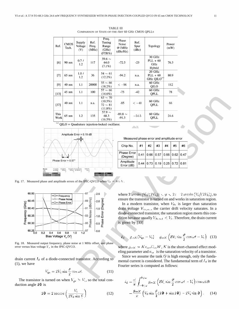
IEEE
Pro
of
Prin
t Ver
sion
YI et al.: A 57.9-TO-68.3 GHz 24.6 mW FREQUENCY SYNTHESIZER WITH IN-PHASE INJECTION-COUPLED QVCO IN 65 nm CMOS TECHNOLOGY 11
TABLE IIICOMPARISON OF STATE-OF-THE-ART 60 GHZ CMOS QPLLS
Fig. 17. Measured phase and amplitude errors of the IPIC-QVCO when .
Fig. 18. Measured output frequency, phase noise at 1 MHz offset, and phaseerror versus bias voltage in the IPIC-QVCO.
drain current of a diode-connected transistor. According to(1), we have
(11)
The transistor is turned on when , so the total con-duction angle is
(12)
where , toensure the transistor is turned on and works in saturation region.
In a modern transistor, when is larger than saturationdrain voltage , the carrier drift velocity saturates. In adiode-connected transistor, the saturation region meets this con-dition because usually . Therefore, the drain currentis given by [33]
(13)
where , is the short-channel effect mod-eling parameter and is the saturation velocity of a transistor.
Since we assume the tank is high enough, only the funda-mental current is considered. The fundamental term of in theFourier series is computed as follows:
(14)
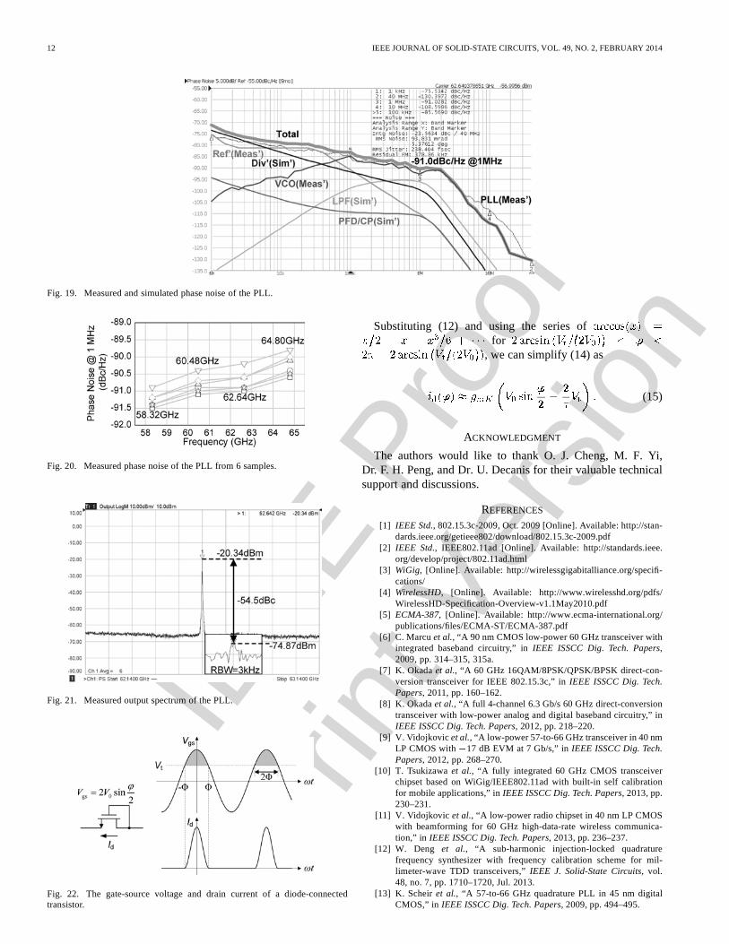
IEEE
Pro
of
Prin
t Ver
sion
12 IEEE JOURNAL OF SOLID-STATE CIRCUITS, VOL. 49, NO. 2, FEBRUARY 2014
Fig. 19. Measured and simulated phase noise of the PLL.
Fig. 20. Measured phase noise of the PLL from 6 samples.
Fig. 21. Measured output spectrum of the PLL.
Fig. 22. The gate-source voltage and drain current of a diode-connectedtransistor.
Substituting (12) and using the series offor
, we can simplify (14) as
(15)
ACKNOWLEDGMENT
The authors would like to thank O. J. Cheng, M. F. Yi,Dr. F. H. Peng, and Dr. U. Decanis for their valuable technicalsupport and discussions.
REFERENCES
[1] IEEE Std., 802.15.3c-2009, Oct. 2009 [Online]. Available: http://stan-dards.ieee.org/getieee802/download/802.15.3c-2009.pdf
[2] IEEE Std., IEEE802.11ad [Online]. Available: http://standards.ieee.org/develop/project/802.11ad.html
[3] WiGig, [Online]. Available: http://wirelessgigabitalliance.org/specifi-cations/
[4] WirelessHD, [Online]. Available: http://www.wirelesshd.org/pdfs/WirelessHD-Specification-Overview-v1.1May2010.pdf
[5] ECMA-387, [Online]. Available: http://www.ecma-international.org/publications/files/ECMA-ST/ECMA-387.pdf
[6] C. Marcu et al., “A 90 nm CMOS low-power 60 GHz transceiver withintegrated baseband circuitry,” in IEEE ISSCC Dig. Tech. Papers,2009, pp. 314–315, 315a.
[7] K. Okada et al., “A 60 GHz 16QAM/8PSK/QPSK/BPSK direct-con-version transceiver for IEEE 802.15.3c,” in IEEE ISSCC Dig. Tech.Papers, 2011, pp. 160–162.
[8] K. Okada et al., “A full 4-channel 6.3 Gb/s 60 GHz direct-conversiontransceiver with low-power analog and digital baseband circuitry,” inIEEE ISSCC Dig. Tech. Papers, 2012, pp. 218–220.
[9] V. Vidojkovic et al., “A low-power 57-to-66 GHz transceiver in 40 nmLP CMOS with 17 dB EVM at 7 Gb/s,” in IEEE ISSCC Dig. Tech.Papers, 2012, pp. 268–270.
[10] T. Tsukizawa et al., “A fully integrated 60 GHz CMOS transceiverchipset based on WiGig/IEEE802.11ad with built-in self calibrationfor mobile applications,” in IEEE ISSCC Dig. Tech. Papers, 2013, pp.230–231.
[11] V. Vidojkovic et al., “A low-power radio chipset in 40 nm LP CMOSwith beamforming for 60 GHz high-data-rate wireless communica-tion,” in IEEE ISSCC Dig. Tech. Papers, 2013, pp. 236–237.
[12] W. Deng et al., “A sub-harmonic injection-locked quadraturefrequency synthesizer with frequency calibration scheme for mil-limeter-wave TDD transceivers,” IEEE J. Solid-State Circuits, vol.48, no. 7, pp. 1710–1720, Jul. 2013.
[13] K. Scheir et al., “A 57-to-66 GHz quadrature PLL in 45 nm digitalCMOS,” in IEEE ISSCC Dig. Tech. Papers, 2009, pp. 494–495.

IEEE
Pro
of
Prin
t Ver
sion
YI et al.: A 57.9-TO-68.3 GHz 24.6 mW FREQUENCY SYNTHESIZER WITH IN-PHASE INJECTION-COUPLED QVCO IN 65 nm CMOS TECHNOLOGY 13
[14] A. Musa et al., “A 58–63.6 GHz quadrature PLL frequency synthesizerin 65 nm CMOS,” in Proc. ASSCC, 2010, pp. 1–4.
[15] X. Yi et al., “A 57.9-to-68.3 GHz 24.6 mW frequency synthesizer within-phase injection-coupled QVCO in 65 nm CMOS,” in IEEE ISSCCDig. Tech. Papers, 2013, pp. 354–355.
[16] A. Mirzaei et al., “The quadrature LC oscillator: A complete portraitbased on injection locking,” IEEE J. Solid-State Circuits, vol. 42, no.9, pp. 1916–1932, Sep. 2007.
[17] U. Decanis et al., “A mm-Wave quadrature VCO based on magnet-ically coupled resonators,” in IEEE ISSCC Dig. Tech. Papers, 2011,pp. 280–282.
[18] J. Van Der Tang et al., “Analysis and design of an optimally coupled5-GHz quadrature LC oscillator,” IEEE J. Solid-State Circuits, vol. 37,no. 5, pp. 657–661, May 2002.
[19] M. Valla et al., “A 72-mW CMOS 802.11a direct conversion front-endwith 3.5-dB NF and 200-kHz 1/f noise corner,” IEEE J. Solid-StateCircuits, vol. 40, no. 4, pp. 970–977, Apr. 2005.
[20] H. Tong et al., “An LC quadrature VCO using capacitive source de-generation coupling to eliminate bi-modal oscillation,” IEEE Trans.Circuits Syst. I, Reg. Papers, vol. 59, no. 9, pp. 1871–1879, Sep. 2012.
[21] U. Decanis et al., “A low-noise quadrature VCO based on magneticallycoupled resonators and a wideband frequency divider at millimeterwaves,” IEEE J. Solid-State Circuits, vol. 46, no. 12, pp. 2943–2955,Dec. 2011.
[22] Q. Gu et al., “A low power V-band CMOS frequency divider withwide locking range and accurate quadrature output phases,” IEEE J.Solid-State Circuits, vol. 43, no. 4, pp. 991–998, Apr. 2008.
[23] X. Yi et al., “Design of ring-oscillator-based injection-locked fre-quency dividers with single-phase inputs,” IEEE Microw. WirelessCompon. Lett., vol. 21, no. 10, pp. 559–561, Oct. 2011.
[24] X. Yi et al., “A divide-by-two injection-locked frequency divider with13-GHz locking range in 0.18- m CMOS technology,” in IEEE Proc.ISIC, Dec. 2011, pp. 216–219.
[25] J. Rael and A. A. Abidi, “Physical processes of phase noise in differen-tial LC oscillators,” in Proc. IEEE Custom Integrated Circuits Conf.,CICC, 2000, pp. 569–572.
[26] P. Andreani et al., “Analysis and design of a 1.8-GHz CMOS LCquadrature VCO,” IEEE J. Solid-State Circuits, vol. 37, no. 12, pp.1737–1747, Dec. 2002.
[27] A. Hajimiri and T. Lee, “A general theory of phase noise in electricaloscillators,” IEEE J. Solid-State Circuits, vol. 33, no. 2, pp. 179–194,Feb. 1998.
[28] D. Murphy et al., “A low phase noise, wideband and compact CMOSPLL for use in a heterodyne 802.15.3c transceiver,” IEEE J. Solid-StateCircuits, vol. 46, no. 7, pp. 1606–1617, Jul. 2011.
[29] P. Andreani and X. Wang, “On the phase-noise and phase-error perfor-mances of multiphase LC CMOS VCOs,” IEEE J. Solid-State Circuits,vol. 39, no. 11, pp. 1883–1893, Nov. 2004.
[30] S. L. J. Gierkink et al., “A low-phase-noise 5-GHz CMOS quadratureVCO using superharmonic coupling,” IEEE J. Solid-State Circuits, vol.38, no. 7, pp. 1148–1154, Jul. 2003.
[31] A. Mirzaei et al., “Multi-phase injection widens lock range of ring-oscillator-based frequency dividers,” IEEE J. Solid-State Circuits, vol.43, no. 3, pp. 656–671, Mar. 2008.
[32] S. L. Gierkink, “Low-spur, low-phase-noise clock multiplier based ona combination of PLL and recirculating DLL with dual-pulse ring os-cillator and self-correcting charge pump,” IEEE J. Solid-State Circuits,vol. 43, no. 12, pp. 2967–2976, Dec. 2008.
[33] K.-Y. Toh et al., “An engineering model for short-channel MOS de-vices,” IEEE J. Solid-State Circuits, vol. 23, no. 4, pp. 950–958, Apr.1988.
[34] A. Rofougaran et al., “A 900 MHz CMOS LC-oscillator with quadra-ture outputs,” in IEEE ISSCC Dig. Tech. Papers, 1996, pp. 392–393.
[35] P. Sakian et al., “A 57–63 GHz quadrature VCO in CMOS 65 nm,” inProc. IEEE EuMIC, 2009, pp. 120–123.
[36] L. Wu and H. Luong, “A 49-to-62 GHz CMOS quadrature VCO withbimodal enhanced magnetic tuning,” in Proc. ESSCIRC, 2012, pp.297–300.
[37] A. Bevilacqua et al., “A 40 nm LP CMOS PLL for high-speedmm-wave communication,” in Proc. ESSCIRC, 2010, pp. 254–257.
Xiang Yi (S’11–M’13) received the B.E. degreefrom Huazhong University of Science and Tech-nology, Wuhan, China, in 2006 and the M.S.degree from South China University of Technology,Guangzhou, China, in 2009. From August 2009to August 2013, he pursued the Ph.D. degree inNanyang Technological University, Singapore.
He is currently working as a Research Asso-ciate in Nanyang Technological University. Hisresearch interests include radio frequency (RF) andmillimeter-wave (mm-wave) phase-locked loops
(PLLs), frequency synthesizers, and transceiver systems.Mr. Yi was the recipient of the IEEE ISSCC Silkroad Award and SSCS Travel
Grant Award in 2013. He is a technical reviewer for several IEEE journals andconferences.
Chirn Chye Boon (M’09–SM’10) received the B.E.(Hons.) (Elect.) in 2000 and the Ph.D. (Elect. Eng.)in 2004 from Nanyang Technological University(NTU), Singapore.
He is the Assistant Professor in NTU and theProgram Director of the S$50 million research centerof excellence, VIRTUS (NTU). He specializes inthe areas of radio frequency (RF) and mm-wavecircuits and systems design for Imaging and Com-munications applications. He has coauthored over 70refereed publications and several patents and books
in the fields of RF and MM-wave.Dr. Boon is an Associate Editor of the IEEE TRANSACTIONS ON VERY LARGE
SCALE INTEGRATION (VLSI) SYSTEMS. He is a winner of Year-2 Teaching Ex-cellent Award, EEE, NTU and IEEE Electron Devices Letters Golden Reviewer.
Hang Liu received the B.E. (Hons.) (Elect.) in 2011from Nanyang Technological University (NTU), Sin-gapore. In 2011, he joined NTU as a Project Officerand enrolled as a part-time Ph.D. student in the sameyear.
He specializes in the areas of radio frequency (RF)circuits and systems design, with main focuses on os-cillator designs in both CMOS and GaN. His researchalso includes power amplifier design, low noise am-plifier design and baseband variable gain amplifierdesign.
Jia Fu Lin (S’13) received the B.S. degree fromAnhui University, Hefei, China, in 2009. He iscurrently working toward the Ph.D. degree at theSchool of Electrical and Electronic Engineering,Nanyang Technological University, Singapore.
His research interests include CMOS RF trans-ceivers and open source hardware design.
Wei Meng Lim received the B.E (Hons.) and M.Edegrees from Nanyang Technology University(NTU), Singapore, in 2002 and 2004, respectively.
Upon his graduation, he joined the School ofElectrical and Electronic Engineering, NTU, as aresearch staff. His research interests include RFcircuit designs, RF devices characterization, andmodeling.