
XCL102 103 ETR28011-001 · PIN ASSIGNMENT FUNCTION CHART ... * If the pad needs to be connected to...
20
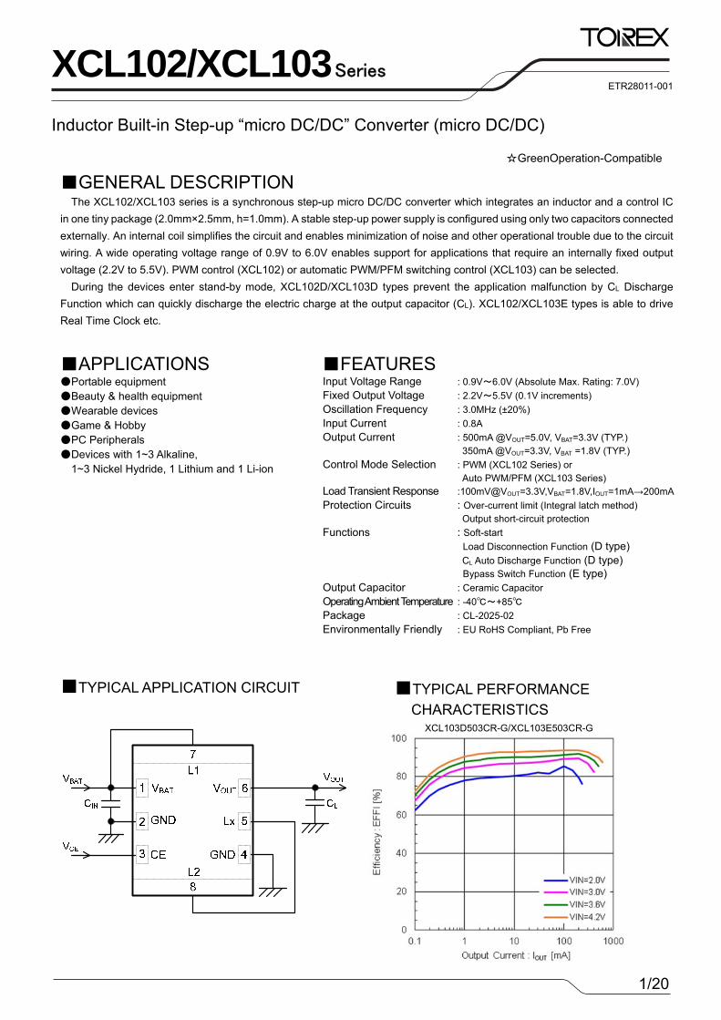
1/20 XCL102/XCL103 Series Inductor Built-in Step-up “micro DC/DC” Converter (micro DC/DC) ■GENERAL DESCRIPTION The XCL102/XCL103 series is a synchronous step-up micro DC/DC converter which integrates an inductor and a control IC in one tiny package (2.0mm×2.5mm, h=1.0mm). A stable step-up power supply is configured using only two capacitors connected externally. An internal coil simplifies the circuit and enables minimization of noise and other operational trouble due to the circuit wiring. A wide operating voltage range of 0.9V to 6.0V enables support for applications that require an internally fixed output voltage (2.2V to 5.5V). PWM control (XCL102) or automatic PWM/PFM switching control (XCL103) can be selected. During the devices enter stand-by mode, XCL102D/XCL103D types prevent the application malfunction by CL Discharge Function which can quickly discharge the electric charge at the output capacitor (CL). XCL102/XCL103E types is able to drive Real Time Clock etc. ■APPLICATIONS ●Portable equipment ●Beauty & health equipment ●Wearable devices ●Game & Hobby ●PC Peripherals ●Devices with 1~3 Alkaline, 1~3 Nickel Hydride, 1 Lithium and 1 Li-ion ■FEATURES Input Voltage Range : 0.9V~6.0V (Absolute Max. Rating: 7.0V) Fixed Output Voltage : 2.2V~5.5V (0.1V increments) Oscillation Frequency : 3.0MHz (±20%) Input Current : 0.8A Output Current : 500mA @V OUT =5.0V, V BAT =3.3V (TYP.) 350mA @V OUT =3.3V, V BAT =1.8V (TYP.) Control Mode Selection Load Transient Response : PWM (XCL102 Series) or Auto PWM/PFM (XCL103 Series) :100mV@V OUT =3.3V,V BAT =1.8V,I OUT =1mA→200mA Protection Circuits : Over-current limit (Integral latch method) Output short-circuit protection Functions : Soft-start Load Disconnection Function (D type) C L Auto Discharge Function (D type) Bypass Switch Function (E type) Output Capacitor : Ceramic Capacitor Operating Ambient Temperature : -40℃~+85℃ Package : CL-2025-02 Environmentally Friendly : EU RoHS Compliant, Pb Free ■TYPICAL APPLICATION CIRCUIT ETR28011-001 ☆GreenOperation-Compatible ■TYPICAL PERFORMANCE CHARACTERISTICS XCL103D503CR-G/XCL103E503CR-G
Transcript of XCL102 103 ETR28011-001 · PIN ASSIGNMENT FUNCTION CHART ... * If the pad needs to be connected to...
1/20
XCL102/XCL103 Series
Inductor Built-in Step-up “micro DC/DC” Converter (micro DC/DC)
GENERAL DESCRIPTION The XCL102/XCL103 series is a synchronous step-up micro DC/DC converter which integrates an inductor and a control IC
in one tiny package (2.0mm×2.5mm, h=1.0mm). A stable step-up power supply is configured using only two capacitors connected externally. An internal coil simplifies the circuit and enables minimization of noise and other operational trouble due to the circuit wiring. A wide operating voltage range of 0.9V to 6.0V enables support for applications that require an internally fixed output voltage (2.2V to 5.5V). PWM control (XCL102) or automatic PWM/PFM switching control (XCL103) can be selected.
During the devices enter stand-by mode, XCL102D/XCL103D types prevent the application malfunction by CL Discharge Function which can quickly discharge the electric charge at the output capacitor (CL). XCL102/XCL103E types is able to drive Real Time Clock etc.
APPLICATIONS Portable equipment Beauty & health equipment Wearable devices Game & Hobby PC Peripherals Devices with 1~3 Alkaline,
1~3 Nickel Hydride, 1 Lithium and 1 Li-ion
FEATURESInput Voltage Range : 0.9V~6.0V (Absolute Max. Rating: 7.0V) Fixed Output Voltage : 2.2V~5.5V (0.1V increments) Oscillation Frequency : 3.0MHz (±20%) Input Current : 0.8A Output Current : 500mA @VOUT=5.0V, VBAT=3.3V (TYP.)
350mA @VOUT=3.3V, VBAT =1.8V (TYP.) Control Mode Selection Load Transient Response
: PWM (XCL102 Series) or Auto PWM/PFM (XCL103 Series) :100mV@VOUT=3.3V,VBAT=1.8V,IOUT=1mA→200mA
Protection Circuits : Over-current limit (Integral latch method) Output short-circuit protection
Functions : Soft-start Load Disconnection Function (D type) CL Auto Discharge Function (D type)
Bypass Switch Function (E type) Output Capacitor : Ceramic Capacitor Operating Ambient Temperature : -40~+85 Package : CL-2025-02 Environmentally Friendly : EU RoHS Compliant, Pb Free
TYPICAL APPLICATION CIRCUIT
ETR28011-001
GreenOperation-Compatible
TYPICAL PERFORMANCE CHARACTERISTICS
XCL103D503CR-G/XCL103E503CR-G
2/20
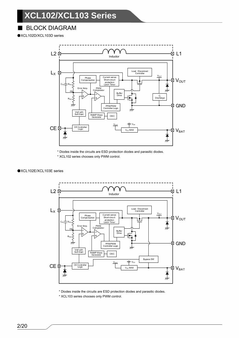
XCL102/XCL103 Series BLOCK DIAGRAM XCL102D/XCL103D series
* Diodes inside the circuits are ESD protection diodes and parasitic diodes. * XCL102 series chooses only PWM control.
XCL102E/XCL103E series
* Diodes inside the circuits are ESD protection diodes and parasitic diodes. * XCL103 series chooses only PWM control.
VDD MAX
RFB1
Load DisconnectController
CE ControllerLogic
PWMComparator
BufferDrive
LX
VBAT
VOUTCurrent senseShort-circuit protection
Latch Timer
Vref withSoft Start
CFB
Inductor
GND
L2 L1
PFM/PWMController Logic
VDD
CE
VOUT
CLDischarge
Error Amp.
PhaseCompensation
RAMP WaveGenerator OSC
RFB2
FB
VOUT
VDD MAX
RFB1
Load DisconnectController
CE ControllerLogic
PWMComparator
BufferDrive
LX
VBAT
VOUTCurrent senseShort-circuit protection
Latch Timer
Vref withSoft Start
CFB
Inductor
GND
L2 L1
PFM/PWMController Logic
VDD
CE
VOUT
Bypass SW
Error Amp.
PhaseCompensation
RAMP WaveGenerator OSC
RFB2
FB
VOUT
3/20
XCL102/XCL103Series
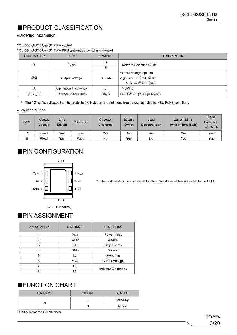
PRODUCT CLASSIFICATION Ordering Information XCL102①②③④⑤⑥-⑦ PWM control XCL103①②③④⑤⑥-⑦ PWM/PFM automatic switching control
Selection guides
PIN CONFIGURATION
PIN ASSIGNMENT
FUNCTION CHART PIN NAME SIGNAL STATUS
CE L Stand-by
H Active
* Do not leave the CE pin open.
DESIGNATOR ITEM SYMBOL DESCRIPTION
① Type D
Refer to Selection Guide E
②③ Output Voltage 22~55 Output Voltage options e.g.)3.3V → ②=3, ③=3 5.0V → ②=5, ③=0
④ Oscillation Frequency 3 3.0MHz
⑤⑥-⑦ (*1) Package (Order Unit) CR-G CL-2025-02 (3,000pcs/Reel)
TYPE Output Voltage
Chip Enable
Soft-Start CL Auto-
Discharge Bypass Switch
Load Disconnection
Current Limit (with integral latch)
Short Protection with latch
D Fixed Yes Fixed Yes No Yes Yes Yes E Fixed Yes Fixed No Yes No Yes Yes
PIN NUMBER PIN NAME FUNCTIONS
1 VBAT Power Input 2 GND Ground 3 CE Chip Enable 4 GND Ground 5 Lx Switching 6 VOUT Output Voltage 7 L1
Inductor Electrodes 8 L2
* If the pad needs to be connected to other pins, it should be connected to the GND.
(*1) The ”-G” suffix indicates that the products are Halogen and Antimony free as well as being fully EU RoHS compliant.
7 L1
8 L2
VOUT 6
Lx 5
GND 4
1 VBA T
2 GND
3 CE
(BOTTOM VIEW)
4/20
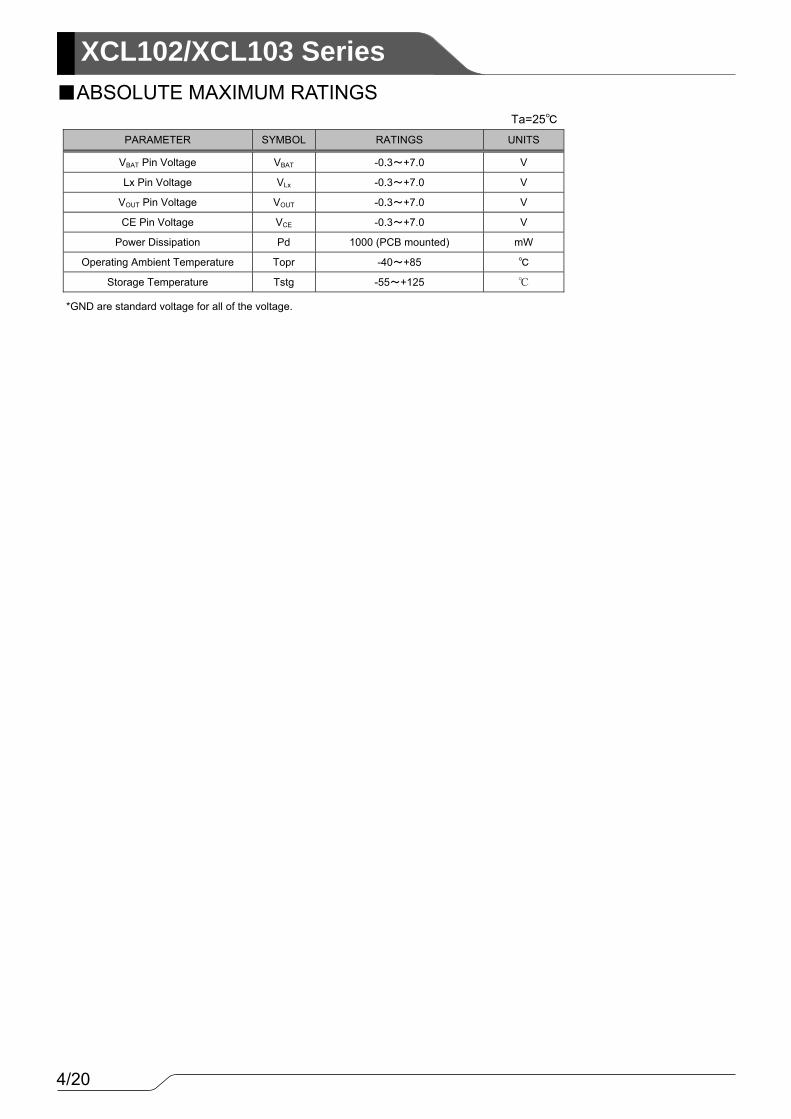
XCL102/XCL103 Series ABSOLUTE MAXIMUM RATINGS
Ta=25
PARAMETER SYMBOL RATINGS UNITS
VBAT Pin Voltage VBAT -0.3~+7.0 V
Lx Pin Voltage VLx -0.3~+7.0 V
VOUT Pin Voltage VOUT -0.3~+7.0 V
CE Pin Voltage VCE -0.3~+7.0 V
Power Dissipation Pd 1000 (PCB mounted) mW
Operating Ambient Temperature Topr -40~+85
Storage Temperature Tstg -55~+125
*GND are standard voltage for all of the voltage.
5/20
XCL102/XCL103Series
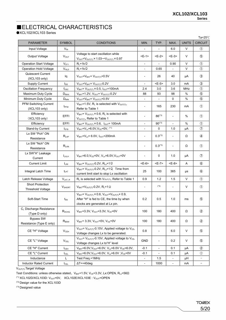
ELECTRICAL CHARACTERISTICS XCL102/XCL103 Series
Ta=25
PARAMETER SYMBOL CONDITIONS MIN. TYP. MAX. UNITS CIRCUIT
Input Voltage VIN - - 6.0 V ①
Output Voltage VOUT Voltage to start oscillation while VOUT=VOUT(T)×1.03→VOUT(T)×0.97
<E-1> <E-2> <E-3> V ⑤
Operation Start Voltage VST1 RL=1kΩ - - 0.90 V ①
Operation Hold Voltage VHLD RL=1kΩ - 0.65 - V ①
Quiescent Current (XCL103 only)
Iq VOUT=VBAT= VOUT(T)+0.5V - 26 40 μA ③
Supply Current IDD VOUT=VBAT= VOUT(T)-0.2V - <E-5> 3.0 mA ③ Oscillation Frequency fOSC VBAT= VOUT(T)×0.5, IOUT=100mA 2.4 3.0 3.6 MHz ①
Maximum Duty Cycle DMAX VBAT=1.2V, VOUT= VOUT(T)-0.2V 88 93 98 % ⑤
Minimum Duty Cycle DMIN VOUT=VBAT= VOUT(T)+0.5V - - 0 % ⑤
PFM Switching Current (XCL103 only)
IPFM VBAT=1.5V, RL is selected with VOUT(T), Refer to Table 1
- 165 230 mA ①
Efficiency (XCL103 only)
EFFI VBAT= VOUT(T)×0.6, RL is selected with VOUT(T), Refer to Table 1
- 86(*3) - % ①
Efficiency EFFI VBAT= VOUT(T)×0.6, IOUT= 100mA - 90(*3) - % ①
Stand-by Current ISTB VBAT=VLx=6.0V,VCE=0V, (*1) - 0 1.0 μA ⑦
Lx SW "Pch" ON Resistance
RLXP VBAT=VLx= 6.0V, IOUT=200mA - 0.3(*2) - Ω ④
Lx SW "Nch" ON Resistance
RLXN - 0.3(*3) - Ω ①
Lx SW”H” Leakage Current
ILXLH VBAT=6.0,VCE=0V, VLx=6.0V,VOUT=0V - 0 1.0 μA ⑦
Current Limit ILIM VBAT= VOUT(T)-0.2V, RLx=1Ω <E-6> <E-7> <E-8> A ⑥
Integral Latch Time tLAT VBAT= VOUT(T)-0.2V, RLx=1Ω, Time from current limit start to stop Lx oscillation
25 100 365 μs ⑥
Latch Release Voltage VLAT_R RL is selected with VOUT(T), Refer to Table 1 0.9 1.2 1.5 V ①
Short Protection Threshold Voltage
VSHORT VBAT=VOUT(T)-0.2V, RL=1Ω - (*3) - V ①
Soft-Start Time tSS VBAT= VOUT(T)×0.6, VOUT=VOUT(T)× 0.9, After "H" is fed to CE, the time by when clocks are generated at Lx pin.
0.2 0.5 1.0 ms ⑤
CL Discharge Resistance (Type D only)
RDCHG VBAT=3.3V, VOUT=3.3V, VCE=0V 100 180 400 Ω ②
Bypass SW Resistance (Type E only)
RBSW VBAT= 3.3V, VOUT=0V, VCE=0V 100 180 400 Ω ②
CE "H" Voltage VCEH VOUT= VOUT(T)-0.15V, Applied voltage to VCE, Voltage changes Lx to be generated.
0.8 - 6.0 V ⑤
CE "L" Voltage VCEL VOUT= VOUT(T)-0.15V, Applied voltage to VCE, Voltage changes Lx to“H” level
GND - 0.2 V ⑤
CE "H" Current ICEH VBAT=6.0V,VOUT=6.0V, VLx=6.0V VCE=6.0V, -0.1 - 0.1 μA ② CE "L" Current ICEL VBAT=6.0V,VOUT=6.0V, VLx=6.0V ,VCE=0V -0.1 - 0.1 μA ②
Inductance L Test Freq.=1MHz - 1.5 - μH -
Inductor Rated Current ICEL ∆T=+40deg - 1000 - mA -
VOUT(T):Target Voltage Test Conditions: unless otherwise stated、VBAT=1.5V, VCE=3.3V, Lx:OPEN, RLx=56Ω (*1) XCL102D/XCL103D: VOUT=0V, XCL102E/XCL103E : VOUT=OPEN (*2) Design value for the XCL103D (*3) Designed value
6/20
XCL102/XCL103 Series
ELECTRICAL CHARACTERISTICS (Continued)
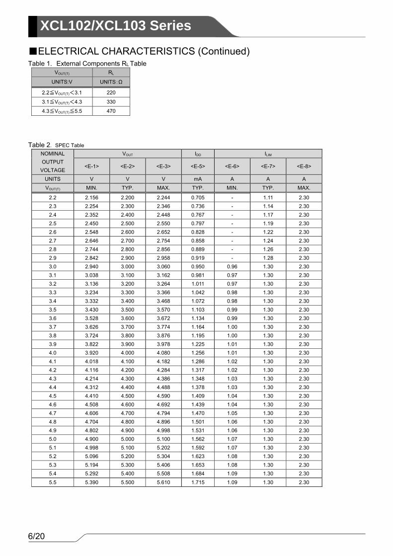
Table 1. External Components RL Table
VOUT(T) RL
UNITS:V UNITS:Ω
2.2≦VOUT(T)<3.1 220
3.1≦VOUT(T)<4.3 330
4.3≦VOUT(T)≦5.5 470
Table 2. SPEC Table
NOMINAL OUTPUT
VOLTAGE
VOUT IDD ILIM
<E-1> <E-2> <E-3> <E-5> <E-6> <E-7> <E-8>
UNITS V V V mA A A A
VOUT(T) MIN. TYP. MAX. TYP. MIN. TYP. MAX.
2.2 2.156 2.200 2.244 0.705 - 1.11 2.30 2.3 2.254 2.300 2.346 0.736 - 1.14 2.30 2.4 2.352 2.400 2.448 0.767 - 1.17 2.30 2.5 2.450 2.500 2.550 0.797 - 1.19 2.30 2.6 2.548 2.600 2.652 0.828 - 1.22 2.30 2.7 2.646 2.700 2.754 0.858 - 1.24 2.30 2.8 2.744 2.800 2.856 0.889 - 1.26 2.30 2.9 2.842 2.900 2.958 0.919 - 1.28 2.30 3.0 2.940 3.000 3.060 0.950 0.96 1.30 2.30 3.1 3.038 3.100 3.162 0.981 0.97 1.30 2.30 3.2 3.136 3.200 3.264 1.011 0.97 1.30 2.30 3.3 3.234 3.300 3.366 1.042 0.98 1.30 2.30 3.4 3.332 3.400 3.468 1.072 0.98 1.30 2.30 3.5 3.430 3.500 3.570 1.103 0.99 1.30 2.30 3.6 3.528 3.600 3.672 1.134 0.99 1.30 2.30 3.7 3.626 3.700 3.774 1.164 1.00 1.30 2.30 3.8 3.724 3.800 3.876 1.195 1.00 1.30 2.30 3.9 3.822 3.900 3.978 1.225 1.01 1.30 2.30 4.0 3.920 4.000 4.080 1.256 1.01 1.30 2.30 4.1 4.018 4.100 4.182 1.286 1.02 1.30 2.30 4.2 4.116 4.200 4.284 1.317 1.02 1.30 2.30 4.3 4.214 4.300 4.386 1.348 1.03 1.30 2.30 4.4 4.312 4.400 4.488 1.378 1.03 1.30 2.30 4.5 4.410 4.500 4.590 1.409 1.04 1.30 2.30 4.6 4.508 4.600 4.692 1.439 1.04 1.30 2.30 4.7 4.606 4.700 4.794 1.470 1.05 1.30 2.30 4.8 4.704 4.800 4.896 1.501 1.06 1.30 2.30 4.9 4.802 4.900 4.998 1.531 1.06 1.30 2.30 5.0 4.900 5.000 5.100 1.562 1.07 1.30 2.30 5.1 4.998 5.100 5.202 1.592 1.07 1.30 2.30 5.2 5.096 5.200 5.304 1.623 1.08 1.30 2.30 5.3 5.194 5.300 5.406 1.653 1.08 1.30 2.30 5.4 5.292 5.400 5.508 1.684 1.09 1.30 2.30
5.5 5.390 5.500 5.610 1.715 1.09 1.30 2.30
7/20
XCL102/XCL103Series
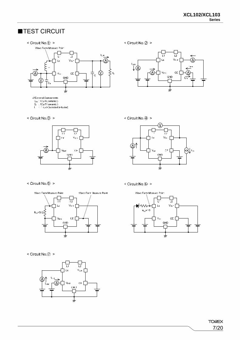
TEST CIRCUIT
8/20
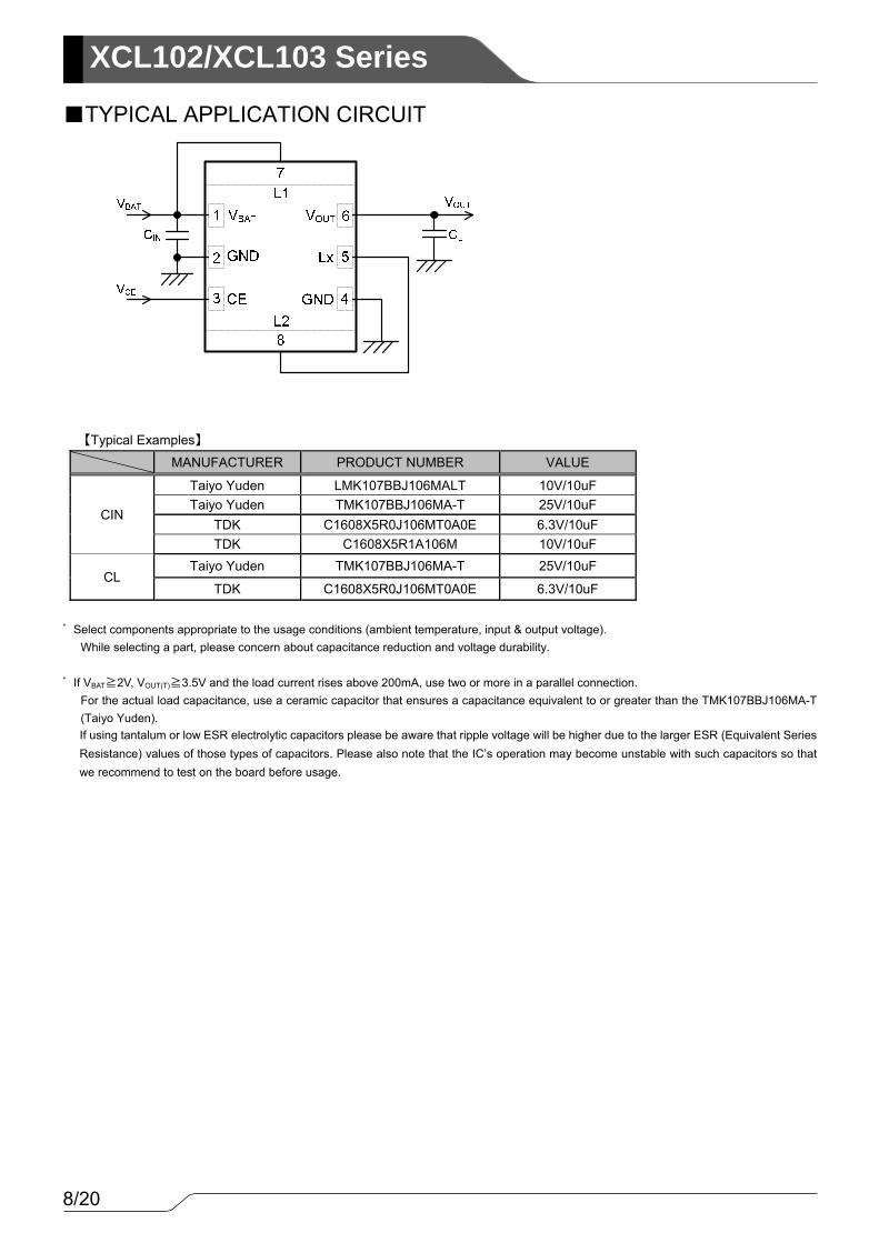
XCL102/XCL103 Series
TYPICAL APPLICATION CIRCUIT
【Typical Examples】
MANUFACTURER PRODUCT NUMBER VALUE
CIN
Taiyo Yuden LMK107BBJ106MALT 10V/10uF Taiyo Yuden TMK107BBJ106MA-T 25V/10uF
TDK C1608X5R0J106MT0A0E 6.3V/10uF TDK C1608X5R1A106M 10V/10uF
CL Taiyo Yuden TMK107BBJ106MA-T 25V/10uF
TDK C1608X5R0J106MT0A0E 6.3V/10uF * Select components appropriate to the usage conditions (ambient temperature, input & output voltage).
While selecting a part, please concern about capacitance reduction and voltage durability.
* If VBAT≧2V, VOUT(T)≧3.5V and the load current rises above 200mA, use two or more in a parallel connection. For the actual load capacitance, use a ceramic capacitor that ensures a capacitance equivalent to or greater than the TMK107BBJ106MA-T (Taiyo Yuden).
If using tantalum or low ESR electrolytic capacitors please be aware that ripple voltage will be higher due to the larger ESR (Equivalent Series Resistance) values of those types of capacitors. Please also note that the IC’s operation may become unstable with such capacitors so that we recommend to test on the board before usage.
9/20
XCL102/XCL103Series
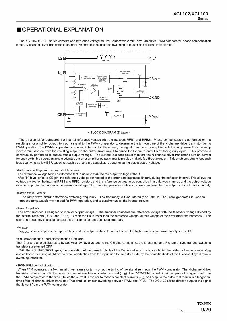
OPERATIONAL EXPLANATION
The XCL102/XCL103 series consists of a reference voltage source, ramp wave circuit, error amplifier, PWM comparator, phase compensation
circuit, N-channel driver transistor, P-channel synchronous rectification switching transistor and current limiter circuit.
The error amplifier compares the internal reference voltage with the resistors RFB1 and RFB2. Phase compensation is performed on the resulting error amplifier output, to input a signal to the PWM comparator to determine the turn-on time of the N-channel driver transistor during PWM operation. The PWM comparator compares, in terms of voltage level, the signal from the error amplifier with the ramp wave from the ramp wave circuit, and delivers the resulting output to the buffer driver circuit to cause the Lx pin to output a switching duty cycle. This process is continuously performed to ensure stable output voltage. The current feedback circuit monitors the N-channel driver transistor’s turn-on current for each switching operation, and modulates the error amplifier output signal to provide multiple feedback signals. This enables a stable feedback loop even when a low ESR capacitor, such as a ceramic capacitor, is used, ensuring stable output voltage. <Reference voltage source, soft start function> The reference voltage forms a reference that is used to stabilize the output voltage of the IC. After “H” level is fed to CE pin, the reference voltage connected to the error amp increases linearly during the soft start interval. This allows the
voltage divided by the internal RFB1 and RFB2 resistors and the reference voltage to be controlled in a balanced manner, and the output voltage rises in proportion to the rise in the reference voltage. This operation prevents rush input current and enables the output voltage to rise smoothly. <Ramp Wave Circuit>
The ramp wave circuit determines switching frequency. The frequency is fixed internally at 3.0MHz. The Clock generated is used to produce ramp waveforms needed for PWM operation, and to synchronize all the internal circuits.
<Error Amplifier> The error amplifier is designed to monitor output voltage. The amplifier compares the reference voltage with the feedback voltage divided by
the internal resistors (RFB1 and RFB2). When the FB is lower than the reference voltage, output voltage of the error amplifier increases. The gain and frequency characteristics of the error amplifier are optimized internally. <VDDMAX>
VDD MAX circuit compares the input voltage and the output voltage then it will select the higher one as the power supply for the IC. <Shutdown function, load disconnection function> The IC enters chip disable state by applying low level voltage to the CE pin. At this time, the N-channel and P-channel synchronous switching transistors are turned OFF With the XCL102D/103D types, the orientation of the parasitic diode of the P-channel synchronous switching transistor is fixed at anode: VOUT and cathode: Lx during shutdown to break conduction from the input side to the output side by the parasitic diode of the P-channel synchronous switching transistor. <PWM/PFM control circuit> When PFM operates, the N-channel driver transistor turns on at the timing of the signal sent from the PWM comparator. The N-channel driver
transistor remains on until the current in the coil reaches a constant current (IPFM). The PWM/PFM control circuit compares the signal sent from the PWM comparator to the time it takes the current in the coil to reach a constant current (IPFM), and outputs the pulse that results in a longer on-time of the N-channel driver transistor. This enables smooth switching between PWM and PFM. The XCL102 series directly outputs the signal that is sent from the PWM comparator.
VDD MAX
RFB1
Load DisconnectController
CE ControllerLogic
PWMComparator
BufferDrive
LX
VBAT
VOUTCurrent senseShort-circuit protection
Latch Timer
Vref withSoft Start
CFB
Inductor
GND
L2 L1
PFM/PWMController Logic
VDD
CE
VOUT
CLDischarge
Error Amp.
PhaseCompensation
RAMP WaveGenerator OSC
RFB2
FB
VOUT
< BLOCK DIAGRAM (D type) >
10/20
XCL102/XCL103 Series
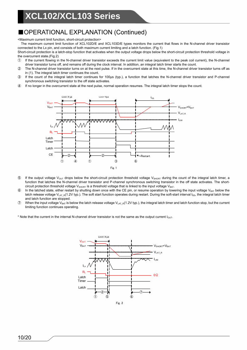
OPERATIONAL EXPLANATION (Continued) <Maximum current limit function, short-circuit protection>
The maximum current limit function of XCL102D/E and XCL103D/E types monitors the current that flows in the N-channel driver transistor connected to the Lx pin, and consists of both maximum current limiting and a latch function. (Fig.1) Short-circuit protection is a latch-stop function that activates when the output voltage drops below the short-circuit protection threshold voltage in the overcurrent state.(Fig.2) ① If the current flowing in the N-channel driver transistor exceeds the current limit value (equivalent to the peak coil current), the N-channel
driver transistor turns off, and remains off during the clock interval. In addition, an integral latch timer starts the count. ② The N-channel driver transistor turns on at the next pulse. If in the overcurrent state at this time, the N-channel driver transistor turns off as
in (1). The integral latch timer continues the count. ③ If the count of the integral latch timer continues for 100μs (typ.), a function that latches the N-channel driver transistor and P-channel
synchronous switching transistor to the off state activates. ④ If no longer in the overcurrent state at the next pulse, normal operation resumes. The integral latch timer stops the count. ⑤ If the output voltage VOUT drops below the short-circuit protection threshold voltage VSHORT during the count of the integral latch timer, a
function that latches the N-channel driver transistor and P-channel synchronous switching transistor in the off state activates. The short-circuit protection threshold voltage VSHORT is a threshold voltage that is linked to the input voltage VBAT.
⑥ In the latched state, either restart by shutting down once with the CE pin, or resume operation by lowering the input voltage VBAT below the latch release voltage VLAT_R(1.2V typ.). The soft start function operates during restart. During the soft-start interval tSS, the integral latch timer and latch function are stopped.
⑦ When the input voltage VBAT is below the latch release voltage VLAT_R(1.2V typ.), the integral latch timer and latch function stop, but the current limiting function continues operating.
* Note that the current in the internal N-channel driver transistor is not the same as the output current IOUT.
ILIM
ILx
VBAT
VOUT
VSHORT=VBAT
Limit< # μs
VLAT_R
RL
Limit= #μs
LatchTimer
Latch
CE Restart
tSS
① ④ ① ③ ⑥
② ②
Fig. 1
ILIM
ILx
VBAT
VOUT
LatchTimer
VSHORT=VBAT
Limit< # μs
VLAT_R
RL
Latch
⑤ ⑥①
② ⑦
Fig. 2
0Ω
11/20
XCL102/XCL103Series
OPERATIONAL EXPLANATION (Continued)
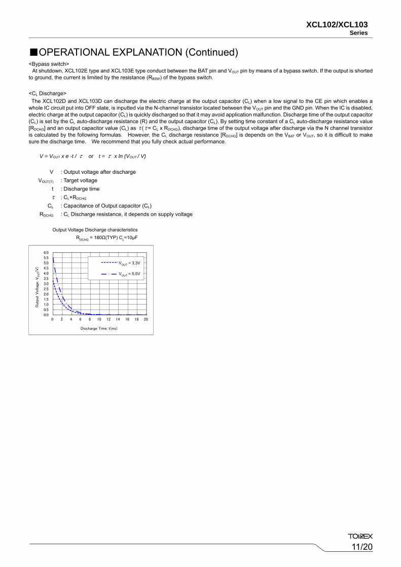
<Bypass switch> At shutdown, XCL102E type and XCL103E type conduct between the BAT pin and VOUT pin by means of a bypass switch. If the output is shorted to ground, the current is limited by the resistance (RBSW) of the bypass switch. <CL Discharge> The XCL102D and XCL103D can discharge the electric charge at the output capacitor (CL) when a low signal to the CE pin which enables a
whole IC circuit put into OFF state, is inputted via the N-channel transistor located between the VOUT pin and the GND pin. When the IC is disabled, electric charge at the output capacitor (CL) is quickly discharged so that it may avoid application malfunction. Discharge time of the output capacitor (CL) is set by the CL auto-discharge resistance (R) and the output capacitor (CL). By setting time constant of a CL auto-discharge resistance value [RDCHG] and an output capacitor value (CL) as τ (τ = CL x RDCHG), discharge time of the output voltage after discharge via the N channel transistor is calculated by the following formulas. However, the CL discharge resistance [RDCHG] is depends on the VBAT or VOUT, so it is difficult to make sure the discharge time. We recommend that you fully check actual performance.
V = VOUT x e -t / τ or t = τ x ln (VOUT / V)
V : Output voltage after discharge VOUT(T) : Target voltage
t : Discharge time τ : CL×RDCHG
CL : Capacitance of Output capacitor (CL) RDCHG : CL Discharge resistance, it depends on supply voltage
0.0
0.5
1.0
1.5
2.0
2.5
3.0
3.5
4.0
4.5
5.0
5.5
6.0
0 2 4 6 8 10 12 14 16 18 20
Outp
ut
Voltag
e: V
OU
T(V
)
Discharge Time: t(ms)
--
---
Output Voltage Discharge characteristics RDCHG = 180Ω(TYP) CL=10μF
VOUT = 3.3V
VOUT = 5.5V
12/20
XCL102/XCL103 Series
NOTE ON USE 1) For the phenomenon of temporal and transitional voltage decrease or voltage increase, the IC may be damaged or deteriorated if IC is used
beyond the absolute maximum ratings. 2) Spike noise and ripple voltage arise in a switching regulator as with a DC/DC converter. These are greatly influenced by external component
selection, such as the capacitance values, and board layout of external components. Once the design has been completed, verification with actual components should be done.
3) The DC/DC converter performance is greatly influenced by not only the ICs' characteristics, but also by those of the external components.
Care must be taken when selecting the external components. Especially for CL load capacitor, it is recommended to use type B capacitors (JIS regulation) or X7R, X5R capacitors (EIA regulation).
4) Use a ground wire of sufficient strength. Ground potential fluctuation caused by the ground current during switching could cause the IC
operation to become unstable, so reinforce the area around the GND pin of the IC in particular. 5) Please mount each external component as close to the IC as possible. Also, please make traces thick and short to reduce the circuit
impedance. 6) With regard to the current limiting value (ILIM), the actual coil current may at times exceed the electrical characteristics due to propagation
delay inside the product. 7) The CE pin is a CMOS input pin. Do not use with the pin open. If connecting to the BAT pin or ground pin, use the resistor which is 1MΩ or
less. To prevent malfunctioning of the device connected to this product or the input/output due to short circuiting between pins, it is recommended that a resistor be connected.
8) The maximum current limiter controls the limit of the N-channel driver transistor by monitoring current flow. This function does not limit the
current flow of the P-channel synchronous transistor. When used with the condition VBAT > VOUT (input voltage higher than the output voltage), the IC may be destroyed if overcurrent flows to the P-channel synchronous switching transistor due to short-circuiting of the load or other reason.
9) When the device is used in high step-up ratio, the current limit function may not work during excessive load current. In this case, the
maximum duty cycle limits maximum current. In this event, latching may not take place, because the maximum current limit cannot be detected.
10) On latch types, some board conditions may cause release from the maximum current limit, and the integrated latch time may become longer or latching may not take place.
11) On latch type, the maximum current limit may be detected, and this will cause the latch function to activate and stop operation after the soft
start time elapses. In particular, note that the soft start time becomes shorter when the IC is used at high temperatures.
12) When the step-up voltage difference is small, the XCL102 series for PWM control may oscillate intermittently. 13) When the voltage boost difference is small, the current limiting function may not operate if the on time of the N-channel driver transistor is
shorter than the propagation delay time of the current limit circuit. In this case, latching may not take place on a latch type because the maximum current limit is not detected.
14) VBAT > VOUT The case and Pch synchronous rectification switch Tr used in (input voltage more expensive than the output voltage). But the
output voltage will be on and becomes equal to input voltage.
15) When connecting large-volume condenser (100 μF) etc. to the loading capacity, a protection circuit of IC moves, and the output voltage doesn't stand up.
16) When input voltage and output voltage are low, integral latch function and short-circuit protection may not operate. We recommend that you fully check actual performance.
17) TOREX places an importance on improving our products and its reliability. However, by any possibility, we would request user fail-safe design and post-aging treatment on system or equipment.
13/20
XCL102/XCL103Series
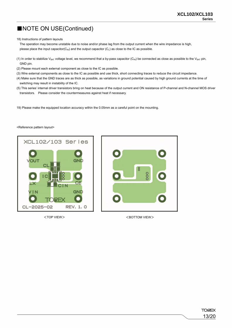
NOTE ON USE(Continued) 18) Instructions of pattern layouts
The operation may become unstable due to noise and/or phase lag from the output current when the wire impedance is high, please place the input capacitor(CIN) and the output capacitor (CL) as close to the IC as possible.
(1) In order to stabilize VBAT voltage level, we recommend that a by-pass capacitor (CIN) be connected as close as possible to the VBAT pin,
GND pin. (2) Please mount each external component as close to the IC as possible. (3) Wire external components as close to the IC as possible and use thick, short connecting traces to reduce the circuit impedance. (4) Make sure that the GND traces are as thick as possible, as variations in ground potential caused by high ground currents at the time of
switching may result in instability of the IC. (5) This series’ internal driver transistors bring on heat because of the output current and ON resistance of P-channel and N-channel MOS driver
transistors. Please consider the countermeasures against heat if necessary. 19) Please make the equipped location accuracy within the 0.05mm as a careful point on the mounting. <Reference pattern layout>
<TOP VIEW> <BOTTOM VIEW>

14/20
XCL102/XCL103 Series
TYPICAL PERFORMANCE CHARACTERISTICS (1) Output Voltage vs Output Current
(2) Efficiency vs Output Current
XCL102D333CR-G/XCL102E333CR-G
XCL102D503CR-G/XCL102E503CR-G XCL103D503CR-G/XCL103E503CR-G
XCL102D333CR-G/XCL102E333CR-G
XCL103D333CR-G/XCL103E333CR-G
XCL103D333CR-G/XCL103E333CR-G
15/20
XCL102/XCL103Series
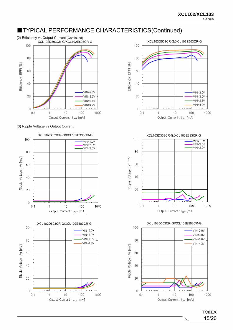
TYPICAL PERFORMANCE CHARACTERISTICS(Continued)
(2) Efficiency vs Output Current (Continued)
(3) Ripple Voltage vs Output Current
XCL102D503CR-G/XCL102E503CR-G XCL103D503CR-G/XCL103E503CR-G
XCL102D503CR-G/XCL102E503CR-G XCL103D503CR-G/XCL103E503CR-G
XCL102D333CR-G/XCL102E333CR-G XCL103D333CR-G/XCL103E333CR-G
16/20
XCL102/XCL103 Series
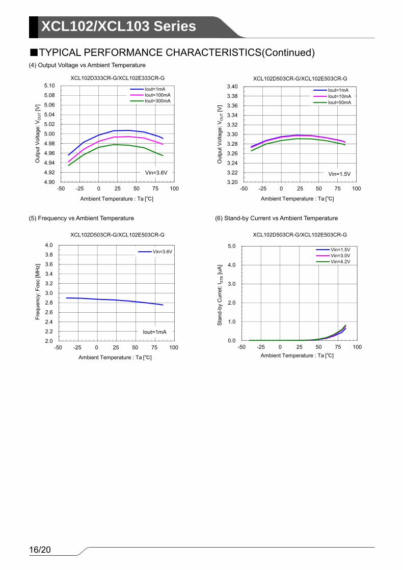
TYPICAL PERFORMANCE CHARACTERISTICS(Continued) (4) Output Voltage vs Ambient Temperature
(5) Frequency vs Ambient Temperature (6) Stand-by Current vs Ambient Temperature
4.90
4.92
4.94
4.96
4.98
5.00
5.02
5.04
5.06
5.08
5.10
-50 -25 0 25 50 75 100
Out
putV
olta
ge: V
OU
T[V
]
Ambient Temperature : Ta []
Iout=1mAIout=100mAIout=300mA
Vin=3.6V
3.20
3.22
3.24
3.26
3.28
3.30
3.32
3.34
3.36
3.38
3.40
-50 -25 0 25 50 75 100
Out
putV
olta
ge: V
OU
T[V
]
Ambient Temperature : Ta []
Iout=1mAIout=10mAIout=50mA
Vin=1.5V
XCL102D333CR-G/XCL102E333CR-G XCL102D503CR-G/XCL102E503CR-G
0.0
1.0
2.0
3.0
4.0
5.0
-50 -25 0 25 50 75 100
Sta
nd-b
y C
urre
t: I S
TB[u
A]
Ambient Temperature : Ta []
Vin=1.5VVin=3.0VVin=4.2V
2.0
2.2
2.4
2.6
2.8
3.0
3.2
3.4
3.6
3.8
4.0
-50 -25 0 25 50 75 100
Freq
uenc
y: F
osc
[MH
z]
Ambient Temperature : Ta []
Vin=3.6V
Iout=1mA
XCL102D503CR-G/XCL102E503CR-G XCL102D503CR-G/XCL102E503CR-G
17/20
XCL102/XCL103Series
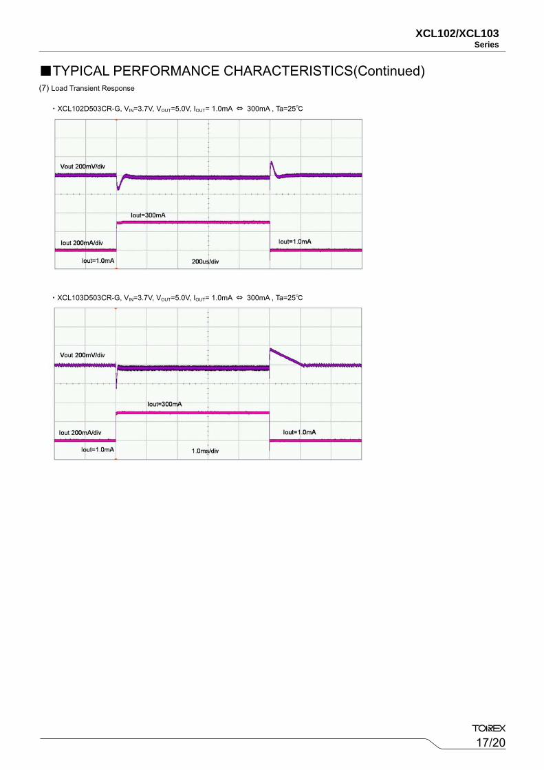
TYPICAL PERFORMANCE CHARACTERISTICS(Continued) (7) Load Transient Response
・XCL102D503CR-G, VIN=3.7V, VOUT=5.0V, IOUT= 1.0mA ⇔ 300mA , Ta=25
・XCL103D503CR-G, VIN=3.7V, VOUT=5.0V, IOUT= 1.0mA ⇔ 300mA , Ta=25
18/20
XCL102/XCL103 Series
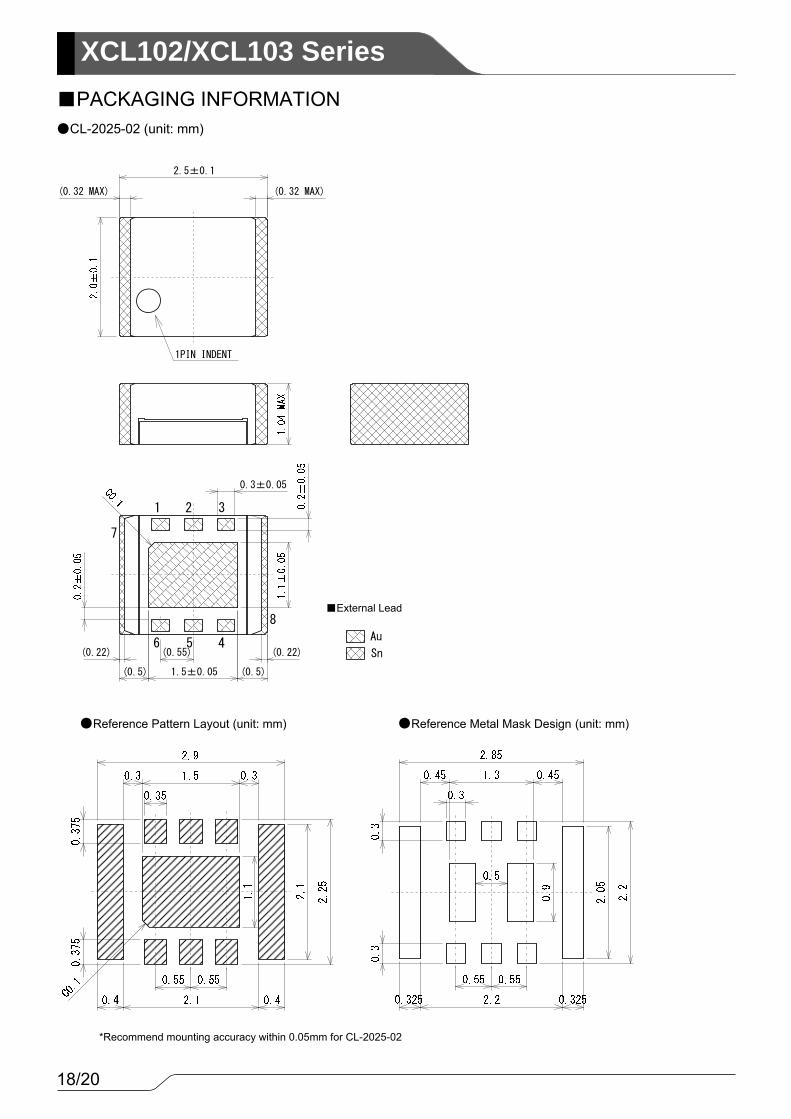
PACKAGING INFORMATION
CL-2025-02 (unit: mm)
*Recommend mounting accuracy within 0.05mm for CL-2025-02
Reference Pattern Layout (unit: mm) Reference Metal Mask Design (unit: mm)
8
7
21 3
6 5 4
2.5±0.1
(0.32 MAX)(0.32 MAX)
0.3±0.05
(0.22)
(0.5) 1.5±0.05 (0.5)
(0.22)(0.55)
外部リード処理
Au
Sn
1PIN INDENT
External Lead
19/20
XCL102/XCL103Series
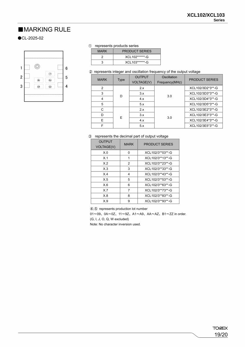
MARKING RULE CL-2025-02
① represents products series
② represents integer and oscillation frequency of the output voltage
③ represents the decimal part of output voltage
④,⑤ represents production lot number 01~09、0A~0Z、11~9Z、A1~A9、AA~AZ、B1~ZZ in order.
(G, I, J, O, Q, W excluded) Note: No character inversion used.
MARK PRODUCT SERIES
2 XCL102******-G 3 XCL103******-G
MARK Type OUTPUT
VOLTAGE(V)Oscillation
Frequency(MHz) PRODUCT SERIES
2
D
2.x
3.0
XCL102/3D2*3**-G 3 3.x XCL102/3D3*3**-G 4 4.x XCL102/3D4*3**-G 5 5.x XCL102/3D5*3**-G C
E
2.x
3.0
XCL102/3E2*3**-G D 3.x XCL102/3E3*3**-G E 4.x XCL102/3E4*3**-G F 5.x XCL102/3E5*3**-G
OUTPUT VOLTAGE(V)
MARK PRODUCT SERIES
X.0 0 XCL102/3**03**-G X.1 1 XCL102/3**13**-G X.2 2 XCL102/3**23**-G X.3 3 XCL102/3**33**-G X.4 4 XCL102/3**43**-G X.5 5 XCL102/3**53**-G X.6 6 XCL102/3**63**-G X.7 7 XCL102/3**73**-G X.8 8 XCL102/3**83**-G X.9 9 XCL102/3**93**-G
⑤④
①②
1
2
3
6
5
4
③
20/20
XCL102/XCL103 Series
1. The product and product specifications contained herein are subject to change without notice to improve performance characteristics. Consult us, or our representatives before use, to confirm that the information in this datasheet is up to date.
2. The information in this datasheet is intended to illustrate the operation and characteristics of our
products. We neither make warranties or representations with respect to the accuracy or completeness of the information contained in this datasheet nor grant any license to any intellectual property rights of ours or any third party concerning with the information in this datasheet.
3. Applicable export control laws and regulations should be complied and the procedures required by
such laws and regulations should also be followed, when the product or any information contained in this datasheet is exported.
4. The product is neither intended nor warranted for use in equipment of systems which require
extremely high levels of quality and/or reliability and/or a malfunction or failure which may cause loss of human life, bodily injury, serious property damage including but not limited to devices or equipment used in 1) nuclear facilities, 2) aerospace industry, 3) medical facilities, 4) automobile industry and other transportation industry and 5) safety devices and safety equipment to control combustions and explosions. Do not use the product for the above use unless agreed by us in writing in advance.
5. Although we make continuous efforts to improve the quality and reliability of our products;
nevertheless Semiconductors are likely to fail with a certain probability. So in order to prevent personal injury and/or property damage resulting from such failure, customers are required to incorporate adequate safety measures in their designs, such as system fail safes, redundancy and fire prevention features.
6. Our products are not designed to be Radiation-resistant.
7. Please use the product listed in this datasheet within the specified ranges.
8. We assume no responsibility for damage or loss due to abnormal use.
9. All rights reserved. No part of this datasheet may be copied or reproduced unless agreed by Torex
Semiconductor Ltd in writing in advance.
TOREX SEMICONDUCTOR LTD.


