Astec AA11040C Electrolytic Capacitors 170429 · 2017. 4. 29. · c24 47µf 250v esr

1/35
XC6701 Series
28V Operation High Speed Voltage Regulators with Stand-by Function
■FEATURESMax Output Current : More than 150mA (200mA limit)
(VIN=VOUT+3.0V) Dropout Voltage : 300mV@IOUT=20mAInput Voltage Range : 2.0V~28.0V Output Voltage Range : 1.8V~18.0V (0.1V increments)High Accuracy : ±2% Low Power Consumption : 50μA (VOUT=5.0V)Stand-by Current : Less than 0.1μAHigh Ripple Rejection : 50dB@1kHz Operating Ambient Temperature : -40℃~+85℃ (XC6701B/D)
-40℃~+105℃(XC6701A) Low ESR Capacitor : Ceramic Capacitor Compatible
(Internal Phase Compensation)Packages : SOT-25, SOT-89, SOT-89-5,
Environmentally Friendly USP-6C, SOT-223, TO-252: EU RoHS Compliant, Pb Free
■GENERAL DESCRIPTION The XC6701 series are positive voltage regulator ICs manufactured using CMOS process with 28V of operation voltage. The series consists of a voltage reference, an error amplifier, a current limiter, a thermal protection circuit and a phase compensation circuit plus a driver transistor. The output voltage is selectable in 0.1V increments within the range of 1.8V to 18V which fixed by laser trimming technologies. The output stabilization capacitor (CL) is also compatible with low ESR ceramic capacitors. The over current protection circuit and the thermal shutdown circuit are built-in. These two protection circuits will operate when the output current reaches current limit level or the junction temperature reaches temperature limit level. The CE function enables the output to be turned off and the IC becomes a stand-by mode resulting in greatly reduced power consumption. Packages are selectable depending on the applications from SOT-25, SOT-89, SOT-89-5, USP-6C, SOT-223, and TO-252.
■APPLICATIONS ●Car audio, Car navigation systems ●Note PCs / Tablet PCs ●Mobile devices / terminals ●Digital still cameras / Camcorders ●Smart phones / Mobile phones ●Multi-function power supplies
■ TYPICAL APPLICATION CIRCUITS ■ TYPICAL PERFORMANCECHARACTERISTICS
ETR0334-012b
XC6701B Series With CE function
XC6701A/B/D 502
4.4
4.5
4.6
4.7
4.8
4.9
5.0
5.1
5.2
5.3
5.4
Time (1ms/div)
Outp
ut
Voltag
e: V
OU
T (
V)
0
30
60
90
120
150
Outp
ut
Curr
ent: I
OU
T (m
A)
Output Current
VIN=7.0V, tr=tf=5μs
CIN=CL=1.0μF (ceramic), Ta=25℃

2/35
XC6701 Series
PIN NUMBER
PIN NAME FUNCTIONS SOT-25 SOT-89-5 USP-6C
1 5 6 VIN Power Input 2 2 5 VSS Ground 3 4 2, 4 NC No connection 4 3 3 CE ON/OFF Control 5 1 1 VOUT Output
PIN NUMBER
PIN NAME FUNCTIONS SOT-89 SOT-223 TO-252
3 3 1 VIN Power Input 2 2 2 VSS Ground 1 1 3 VOUT Output
*CE pin should not be left open. Each should have a certain voltage.
CE(Chip Enable) IC Operation State ON/OFF CE"H" Level Operation ON CE"L" Level Operation OFF CE"OPEN" Operation Undefined
■PIN CONFIGURATION
■PIN ASSIGNMENT
* The dissipation pad for the USP-6C package should be solder-plated in reference mount pattern and metal masking so as to enhance mounting strength and heat release. If the pad needs to be connected to other pins, it should be connected to the VSS (No. 5) pin.
●XC6701A/B Series
●XC6701D Series
■PIN FUNCTION ASSIGNMENT ●XC6701A/B Series
SOT-89-5(TOP VIEW)
SOT-89(TOP VIEW)
1 2 3
VINVOUT VSS
1 2 3
45 2
VOUT VSS CE
VIN NC
TO252(TOP VIEW)
1
2
3
VIN VSS VOUT
USP-6C(BOTTOM VIEW)
3
2
16
5
4
VIN
VSS
NC CE
VOUT
NC
1 32
5 4
VOUT CE
VIN VSS NC
SOT-25(TOP VIEW)
1 2 3
VINVSSVOUT
SOT-223(TOP VIEW)
2
2
2
TO-252
(TOP VIEW)

3/35
XC6701Series
XC6701①②③④⑤⑥‐⑦(*1)
DESIGNATOR ITEM SYMBOL DESCRIPTION
① Type A Fixed Output Voltage, Active High (-40℃≦Topr≦105℃) B Fixed Output Voltage, Active High (-40℃≦Topr≦85℃) D Fixed Output Voltage, No CE function (-40℃≦Topr≦85℃)
②③ Output Voltage 18~J0
For the voltage within 1.8V ~9.9V; e.g. 2.5V ⇒ 25 5.0V ⇒ 50 For the voltage above 10.0V;
e.g. 11.6V ⇒ B6 15.2V ⇒ F2
18.0V ⇒ J0
④ Output Voltage
Accuracy 2 ±2% accuracy
⑤⑥-⑦(*1) Packages
(Order Unit)
MR-G SOT-25 (3,000pcs/Reel) (Only Type A,B) PR-G SOT-89-5 (1,000pcs/Reel) (Only Type A,B) ER-G USP-6C (3,000pcs/Reel) (Only Type A,B) FR-G SOT-223 (1,000pcs/Reel) (Only Type D) JR-G TO-252 (2,500pcs/Reel) (Only Type D) PR-G SOT-89 (1,000pcs/Reel) (Only Type D)
■ PRODUCT CLASSIFICATION ●Ordering Information
(*1) The “-G” suffix denotes Halogen and Antimony free as well as being fully EU RoHS compliant.
■ BLOCK DIAGRAMS
●XC6701A/B Series (SOT-25, SOT-89-5, USP-6C)
●XC6701D Series (SOT-89, SOT-223, TO-252)

4/35
XC6701 Series
PARAMETER SYMBOL RATINGS UNIT Input Voltage VIN VSS-0.3~30 V
Output Current IOUT 300 (*1) mA Output Voltage VOUT VSS-0.3~VIN+0.3 V
CE Input Voltage VCE VSS-0.3~30 V
Power Dissipation
SOT-25
Pd
250
mW
600 (PCB mounted) (*2)
SOT-89-5 500
1300 (PCB mounted) (*2)
USP-6C 120
1000 (PCB mounted) (*2) Operating Ambient Temperature Topr -40~+105 ℃
Storage Temperature Tstg -55~+125 ℃
PARAMETER SYMBOL RATINGS UNIT Input Voltage VIN VSS-0.3~30 V
Output Current IOUT 300 (*1) mA Output Voltage VOUT VSS-0.3~VIN+0.3 V
Power Dissipation
SOT-89
Pd
500
mW
1000 (PCB mounted) (*2)
SOT-223 300
1500 (PCB mounted) (*2)
TO-252 500
1800 (PCB mounted) (*2) Operating Ambient Temperature Topr -40~+85 ℃
Storage Temperature Tstg -55~+125 ℃
PARAMETER SYMBOL RATINGS UNIT Input Voltage VIN VSS-0.3~30 V
Output Current IOUT 300 (*1) mA Output Voltage VOUT VSS-0.3~VIN+0.3 V
CE Input Voltage VCE VSS-0.3~30 V
Power Dissipation
SOT-25
Pd
250
mW
600 (PCB mounted) (*2)
SOT-89-5 500
1300 (PCB mounted) (*2)
USP-6C 120
1000 (PCB mounted) (*2) Operating Ambient Temperature Topr -40~+85 ℃
Storage Temperature Tstg -55~+125 ℃
■ABSOLUTE MAXIMUM RATINGS
●XC6701B Series
●XC6701D Series
*1: IOUT≦Pd / (VIN-VOUT) *2: The power dissipation figure shown is PCB mounted. Please refer to page 27 for details.
●XC6701A Series
*1: IOUT≦Pd / (VIN-VOUT) *2: The power dissipation figure shown is PCB mounted. Please refer to page 27 for details.
Ta=25℃
*1: IOUT≦Pd / (VIN-VOUT) *2: The power dissipation figure shown is PCB mounted. Please refer to page 27 for details.
Ta=25℃
Ta=25℃

5/35
XC6701Series
PARAMETER SYMBOL CONDITIONS MIN. TYP. MAX. UNIT CIRCUIT
Output Voltage VOUT(E) IOUT=10mA, VCE=VIN E2-0 V ①
Maximum Output Current IOUTMAX
VIN= VOUT(T)+3.0V , VCE=VIN (VOUT(T)≧3.0V) 150 - - mA ①
VIN=VOUT(T)+3.0V, VCE=VIN (VOUT(T)<3.0V) 100 - - mA ①
Load Regulation △VOUT
1mA≦IOUT≦50mA , VCE=VIN 1.8V≦VOUT(T)≦5.0V - 50 90
mV ① 1mA≦IOUT≦50mA , VCE=VIN 5.1V≦VOUT(T)≦12.0V - 110 175
1mA≦IOUT≦50mA , VCE=VIN 12.1V≦VOUT(T)≦18.0V - 180 275
Dropout Voltage 1 Vdif1 IOUT=20mA, VCE=VIN E2-1 mV ① Dropout Voltage 2 Vdif2 IOUT=100mA ,VCE=VIN E2-2 mV ①
Supply Current ISS 1.8V≦VOUT(T)≦5.0V 11 50 105
μA ② 5.1V≦VOUT(T)≦12.0V 11 60 115 12.1V≦VOUT(T)≦18.0V 11 65 125
Stand-by Current ISTB VCE=VSS - 0.01 0.10 μA ②
Line Regulation 1 △VOUT/
(△VIN・VOUT) VOUT(T)+2.0V≦VIN≦28.0V IOUT=5mA , VCE=VIN - 0.05 0.10 %/V ①
Line Regulation 2 △VOUT/
(△VIN・VOUT) VOUT(T)+2.0V≦VIN≦28.0V IOUT=13mA , VCE=VIN - 0.15 0.30 %/V ①
Input Voltage VIN 2.0 - 28.0 V -
Output Voltage Temperature Characteristics
△VOUT/ (△Ta・VOUT)
IOUT=20mA, VCE=VIN
XC6701A -40℃≦Ta≦105℃
- ±100 - ppm/℃ ① XC6701B -40℃≦Ta≦85℃
Power Supply Rejection Ratio
PSRR VIN=[VOUT(T)+2.0V]VDC+0.5VP-PAC
IOUT=20mA , f=1kHz , VCE=VIN - 50 - dB ③
Short Current ISHORT VIN=VOUT(T)+2.0V , VCE=VIN - 40 - mA ① CE ”H” Level Voltage VCEH VIN=28.0V 1.1 - 28.0 V ① CE ”L” Level Voltage VCEL VIN=28.0V 0 - 0.35 V ① CE ”H” Level Current ICEH VIN=VCE=28.0V -0.1 - 0.1 μA ① CE ”L” Level Current ICEL VIN=28.0V, VCE=VSS -0.1 - 0.1 μA ① Thermal Shutdown Detect Temperature
TTSD Junction Temperature - 150 - ℃ ①
Thermal Shutdown Release Temperature
TTSR Junction Temperature - 125 - ℃ ①
Hysteresis Width TTSD-TTSR Junction Temperature - 25 - ℃ -
NOTE: *1: VOUT(T): Nominal output voltage *2: VOUT(E): Effective output voltage (i.e. the output voltage when “VOUT(T)+2.0V” is provided at the VIN pin while maintaining a certain IOUT value.) *3: Vdif={VIN1
{Note 5} - VOUT1 {Note 4}} *4: VOUT1: In case of VOUT(T) < 3.0V, the VOUT1 is equal to 98% of the VOUT(T) when a stabilized input voltage is applied in VOUT(T)+3.0V. : In case of VOUT(T)≧3.0V, the VOUT1 is equal to 98% of the VOUT(T) when a stabilized input voltage is applied in VOUT(T)+2.0V. *5: VIN1: The input voltage when VOUT1 appears as input voltage is gradually decreased. *6: Unless otherwise stated, VIN=VOUT(T)+2.0V.
●XC6701A/Bxx2 Series
■ELECTRICAL CHARACTERISTICS
Ta=25℃
6/35
XC6701 Series
PARAMETER SYMBOL CONDITIONS MIN. TYP. MAX. UNIT CIRCUIT
Output Voltage VOUT(E) IOUT=10mA E2-0 V ①
Maximum Output Current IOUTMAX
VIN= VOUT(T)+3.0V (VOUT(T)≧3.0V) 150 - - mA ①
VIN=VOUT(T)+3.0V (VOUT(T)<3.0V ) 100 - - mA ①
Load Regulation △VOUT
1mA≦IOUT≦50mA 1.8V≦VOUT(T)≦5.0V - 50 90
mV ① 1mA≦IOUT≦50mA 5.1V≦VOUT(T)≦12.0V - 110 175
1mA≦IOUT≦50mA 12.1V≦VOUT(T)≦18.0V - 180 275
Dropout Voltage1 Vdif1 IOUT=20mA E2-1 mV ① Dropout Voltage2 Vdif2 IOUT =100mA E2-2 mV ①
Supply Current ISS 1.8V≦VOUT(T)≦5.0V 11 50 105
μA ② 5.1V≦VOUT(T)≦12.0V 11 60 115 12.1V≦VOUT(T)≦18.0V 11 65 125
Line Regulation1 △VOUT/
(△VIN・VOUT) VOUT(T)+2.0V≦VIN≦28.0V IOUT=5mA - 0.05 0.10 %/V ①
Line Regulation2 △VOUT/
(△VIN・VOUT) VOUT(T)+2.0V≦VIN≦28.0V IOUT=13mA - 0.15 0.30 %/V ①
Input Voltage VIN 2.0 - 28.0 V - Output Voltage
Temperature Characteristics △VOUT/
(△Ta・VOUT) IOUT=20mA -40℃≦Ta≦85℃ - ±100 - ppm/℃ ①
Power Supply Rejection Ratio
PSRR VIN=[VOUT(T)+2.0V]+0.5VP-PAC IOUT=20mA , f=1kHz - 50 - dB ③
Short Current ISHORT VIN=VOUT(T)+2.0V - 40 - mA ① Thermal Shutdown Detect
Temperature TTSD Junction Temperature - 150 - ℃ ①
Thermal Shutdown Release Temperature
TTSR Junction Temperature - 125 - ℃ ①
Hysteresis Width TTSD-TTSR Junction Temperature - 25 - ℃ -
■ELECTRICAL CHARACTERISTICS (Continued)
●XC6701Dxx2 Series
NOTE: *1: VOUT(T): Nominal output voltage *2: VOUT(E): Effective output voltage (i.e. the output voltage when “VOUT(T)+2.0V” is provided at the VIN pin while maintaining a certain IOUT value.) *3: Vdif={VIN1
{Note 5} - VOUT1 {Note 4}}
*4: VOUT1: In case of VOUT(T) < 3.0V, the VOUT1 is equal to 98% of the VOUT(T) when a stabilized input voltage is applied in VOUT(T)+3.0V. : In case of VOUT(T)≧3.0V, the VOUT1 is equal to 98% of the VOUT(T) when a stabilized input voltage is applied in VOUT(T)+2.0V. *5: VIN1: The input voltage when VOUT1 appears as input voltage is gradually decreased. *6: Unless otherwise stated, VIN=VOUT(T)+2.0V.
Ta=25℃

7/35
XC6701Series
SYMBOL E2-0 E2-1 E2-2 PARAMETER
NOMINAL OUTPUT VOLTAGE (V)
OUTPUT VOLTAGE(V) (2% products)
DROPOUT VOLTAGE 1 (mV)
IOUT=20mA
DROPOUT VOLTAGE 2 (mV)
IOUT=100mA
VOUT(T) (V)
VOUT Vdif1 Vdif2 MIN. MAX. TYP. MAX. TYP. MAX.
1.8 1.764 1.836 550 710 2200 2700 1.9 1.862 1.938 550 710 2200 2700 2.0 1.960 2.040 450 600 1900 2600 2.1 2.058 2.142 450 600 1900 2600 2.2 2.156 2.244 390 520 1700 2200 2.3 2.254 2.346 390 520 1700 2200 2.4 2.352 2.448 390 520 1700 2200 2.5 2.450 2.550 310 450 1500 1900 2.6 2.548 2.652 310 450 1500 1900 2.7 2.646 2.754 310 450 1500 1900 2.8 2.744 2.856 310 450 1500 1900 2.9 2.842 2.958 310 450 1500 1900 3.0 2.940 3.060 260 360 1300 1700 3.1 3.038 3.162 260 360 1300 1700 3.2 3.136 3.264 260 360 1300 1700 3.3 3.234 3.366 260 360 1300 1700 3.4 3.332 3.468 260 360 1300 1700 3.5 3.430 3.570 260 360 1300 1700 3.6 3.528 3.672 260 360 1300 1700 3.7 3.626 3.774 260 360 1300 1700 3.8 3.724 3.876 260 360 1300 1700 3.9 3.822 3.978 260 360 1300 1700 4.0 3.920 4.080 220 320 1100 1500 4.1 4.018 4.182 220 320 1100 1500 4.2 4.116 4.284 220 320 1100 1500 4.3 4.214 4.386 220 320 1100 1500 4.4 4.312 4.488 220 320 1100 1500 4.5 4.410 4.590 220 320 1100 1500 4.6 4.508 4.692 220 320 1100 1500 4.7 4.606 4.794 220 320 1100 1500 4.8 4.704 4.896 220 320 1100 1500 4.9 4.802 4.998 220 320 1100 1500 5.0 4.900 5.100 190 280 1000 1300 5.1 4.998 5.202 190 280 1000 1300 5.2 5.096 5.304 190 280 1000 1300 5.3 5.194 5.406 190 280 1000 1300 5.4 5.292 5.508 190 280 1000 1300 5.5 5.390 5.610 190 280 1000 1300 5.6 5.488 5.712 190 280 1000 1300 5.7 5.586 5.814 190 280 1000 1300 5.8 5.684 5.916 190 280 1000 1300 5.9 5.782 6.018 190 280 1000 1300 6.0 5.880 6.120 190 280 1000 1300
●Voltage Chart
■ELECTRICAL CHARACTERISTICS (Continued)

8/35
XC6701 Series
SYMBOL E2-0 E2-1 E2-2 PARAMETER
NOMINAL OUTPUT VOLTAGE (V)
OUTPUT VOLTAGE(V) (2% products)
DROPOUT VOLTAGE 1 (mV)
IOUT=20mA
DROPOUT VOLTAGE 2 (mV)
IOUT=100mA
VOUT(T) (V)
VOUT Vdif1 Vdif2 MIN. MAX. TYP. MAX. TYP. MAX.
6.1 5.978 6.222 190 280 1000 1300 6.2 6.076 6.324 190 280 1000 1300 6.3 6.174 6.426 190 280 1000 1300 6.4 6.272 6.528 190 280 1000 1300 6.5 6.370 6.630 170 230 800 1150 6.6 6.468 6.732 170 230 800 1150 6.7 6.566 6.834 170 230 800 1150 6.8 6.664 6.936 170 230 800 1150 6.9 6.762 7.038 170 230 800 1150 7.0 6.860 7.140 170 230 800 1150 7.1 6.958 7.242 170 230 800 1150 7.2 7.056 7.344 170 230 800 1150 7.3 7.154 7.446 170 230 800 1150 7.4 7.252 7.548 170 230 800 1150 7.5 7.350 7.650 170 230 800 1150 7.6 7.448 7.752 170 230 800 1150 7.7 7.546 7.854 170 230 800 1150 7.8 7.644 7.956 170 230 800 1150 7.9 7.742 8.058 170 230 800 1150 8.0 7.840 8.160 170 230 800 1150 8.1 7.938 8.262 130 190 700 950 8.2 8.036 8.364 130 190 700 950 8.3 8.134 8.466 130 190 700 950 8.4 8.232 8.568 130 190 700 950 8.5 8.330 8.670 130 190 700 950 8.6 8.428 8.772 130 190 700 950 8.7 8.526 8.874 130 190 700 950 8.8 8.624 8.976 130 190 700 950 8.9 8.722 9.078 130 190 700 950 9.0 8.820 9.180 130 190 700 950 9.1 8.918 9.282 130 190 700 950 9.2 9.016 9.384 130 190 700 950 9.3 9.114 9.486 130 190 700 950 9.4 9.212 9.588 130 190 700 950 9.5 9.310 9.690 130 190 700 950 9.6 9.408 9.792 130 190 700 950 9.7 9.506 9.894 130 190 700 950 9.8 9.604 9.996 130 190 700 950 9.9 9.702 10.098 130 190 700 950
10.0 9.800 10.200 130 190 700 950
■ELECTRICAL CHARACTERISTICS (Continued)
●Voltage Chart (Continued)

9/35
XC6701Series
SYMBOL E2-0 E2-1 E2-2 PARAMETER
NOMINAL OUTPUT VOLTAGE (V)
OUTPUT VOLTAGE(V) (2% products)
DROPOUT VOLTAGE 1 (mV)
IOUT=20mA
DROPOUT VOLTAGE 2 (mV)
IOUT=100mA
VOUT(T) (V)
VOUT Vdif1 Vdif2 MIN. MAX. TYP. MAX. TYP. MAX.
10.1 9.898 10.302 120 170 650 850 10.2 9.996 10.404 120 170 650 850 10.3 10.094 10.506 120 170 650 850 10.4 10.192 10.608 120 170 650 850 10.5 10.290 10.710 120 170 650 850 10.6 10.388 10.812 120 170 650 850 10.7 10.486 10.914 120 170 650 850 10.8 10.584 11.016 120 170 650 850 10.9 10.682 11.118 120 170 650 850 11.0 10.780 11.220 120 170 650 850 11.1 10.878 11.322 120 170 650 850 11.2 10.976 11.424 120 170 650 850 11.3 11.074 11.526 120 170 650 850 11.4 11.172 11.628 120 170 650 850 11.5 11.270 11.730 120 170 650 850 11.6 11.368 11.832 120 170 650 850 11.7 11.466 11.934 120 170 650 850 11.8 11.564 12.036 120 170 650 850 11.9 11.662 12.138 120 170 650 850 12.0 11.760 12.240 120 170 650 850 12.1 11.858 12.342 120 170 650 850 12.2 11.956 12.444 120 170 650 850 12.3 12.054 12.546 120 170 650 850 12.4 12.152 12.648 120 170 650 850 12.5 12.250 12.750 120 170 650 850 12.6 12.348 12.852 120 170 650 850 12.7 12.446 12.954 120 170 650 850 12.8 12.544 13.056 120 170 650 850 12.9 12.642 13.158 120 170 650 850 13.0 12.740 13.260 120 170 650 850 13.1 12.838 13.362 120 170 650 850 13.2 12.936 13.464 120 170 650 850 13.3 13.034 13.566 120 170 650 850 13.4 13.132 13.668 120 170 650 850 13.5 13.230 13.770 120 170 650 850 13.6 13.328 13.872 120 170 650 850 13.7 13.426 13.974 120 170 650 850 13.8 13.524 14.076 120 170 650 850 13.9 13.622 14.178 120 170 650 850 14.0 13.720 14.280 120 170 650 850
●Voltage Chart (Continued) ■ELECTRICAL CHARACTERISTICS (Continued)

10/35
XC6701 Series
SYMBOL E2-0 E2-1 E2-2 PARAMETER
NOMINAL OUTPUT VOLTAGE (V)
OUTPUT VOLTAGE(V) (2% products)
DROPOUT VOLTAGE 1 (mV)
IOUT=20mA
DROPOUT VOLTAGE 2 (mV)
IOUT=100mA
VOUT(T) (V)
VOUT Vdif1 Vdif2 MIN. MAX. TYP. MAX. TYP. MAX.
14.1 13.818 14.382 120 170 650 850 14.2 13.916 14.484 120 170 650 850 14.3 14.014 14.586 120 170 650 850 14.4 14.112 14.688 120 170 650 850 14.5 14.210 14.790 120 170 650 850 14.6 14.308 14.892 120 170 650 850 14.7 14.406 14.994 120 170 650 850 14.8 14.504 15.096 120 170 650 850 14.9 14.602 15.198 120 170 650 850 15.0 14.700 15.300 120 170 650 850 15.1 14.798 15.402 120 170 650 850 15.2 14.896 15.504 120 170 650 850 15.3 14.994 15.606 120 170 650 850 15.4 15.092 15.708 120 170 650 850 15.5 15.190 15.810 120 170 650 850 15.6 15.288 15.912 120 170 650 850 15.7 15.386 16.014 120 170 650 850 15.8 15.484 16.116 120 170 650 850 15.9 15.582 16.218 120 170 650 850 16.0 15.680 16.320 120 170 650 850 16.1 15.778 16.422 120 170 650 850 16.2 15.876 16.524 120 170 650 850 16.3 15.974 16.626 120 170 650 850 16.4 16.072 16.728 120 170 650 850 16.5 16.170 16.830 120 170 650 850 16.6 16.268 16.932 120 170 650 850 16.7 16.366 17.034 120 170 650 850 16.8 16.464 17.136 120 170 650 850 16.9 16.562 17.238 120 170 650 850 17.0 16.660 17.340 120 170 650 850 17.1 16.758 17.442 120 170 650 850 17.2 16.856 17.544 120 170 650 850 17.3 16.954 17.646 120 170 650 850 17.4 17.052 17.748 120 170 650 850 17.5 17.150 17.850 120 170 650 850 17.6 17.248 17.952 120 170 650 850 17.7 17.346 18.054 120 170 650 850 17.8 17.444 18.156 120 170 650 850 17.9 17.542 18.258 120 170 650 850 18.0 17.640 18.360 120 170 650 850
■OUTPUT VOLTAGE CHART (Continued) ●Voltage Chart (Continued)

11/35
XC6701Series
■ OPERATIONAL EXPLANATION
<Output Voltage Control> The voltage divided by resistors R1 & R2 is compared with the internal reference voltage by the error amplifier. TheP-channel MOSFET, which is connected to the VOUT pin, is then driven by the subsequent output signal. The output voltage at the VOUT pin is controlled and stabilized by a system of negative feedback. The current limit circuit, short protect circuit and thermal protection circuit operate in relation to the level of output current and heat generation. Further, the IC’s internal circuitry can be shutdown via the CE pin’s signal.
<Short-Circuit Protection>
The XC6701 series includes a current fold-back circuit as a short circuit protection. When the load current reaches the current limit level, the current fold-back circuit operates and output voltage drops. The output voltage drops further and output current decreases. When the output pin is shorted, a current of about 30mA flows.
<CE Pin>
The IC’s internal circuitry can be shutdown via the signal from the CE pin with the XC6701A/B series. In shutdown mode, output at the VOUT pin will be pulled down by R1 and R2 to the VSS level. Note that as the XC6701B series’ operations will become unstable with the CE pin open. We suggest that you use this IC with either a VIN voltage or a VSS voltage input at the CE pin. If this IC is used with the correct specifications for the CE pin, the operational logic is fixed and the IC will operate normally. However, supply current may increase as a result of through current in the IC’s internal circuitry if a medium voltage is applied.
<Thermal Shutdown>
When the junction temperature of the built-in driver transistor reaches the temperature limit level (150℃ TYP.), the thermal protection circuit operates and the driver transistor will be set to OFF. The IC resumes its operation when the thermal shutdown function is released and the IC’s operation is automatically restored because the junction temperature drops to the level of the thermal shutdown release voltage.
<Minimum Operating Voltage>
For the stable operation of the IC, over 2.0V of input voltage is necessary. The output voltage may not be generated normally if the input voltage is less than 2.0V.
1. For temporary, transitional voltage drop or voltage rising phenomenon, the IC is liable to malfunction should the ratings be exceeded.
2. Where wiring impedance is high, operations may become unstable due to the noise and/or phase lag depending on output current. Please strengthen VIN and VSS wiring in particular.
3. Phase compensation inside the IC is performed in the XC6701 series. Therefore, an abnormal oscillation does not occur even if there is no output capacitor CL. An input capacitor CIN around 0.1μF~1.0μF between the VIN pin and the VSS pin is required for input stability. Also, the output voltage fluctuation such as under shoot or over shoot, which occurs because of the load change can be controlled by placing the output capacitor CL around 0.1μF~1.0μF between the VOUT pin and VSS pin. The input capacitor (CIN) and the output capacitor (CL) should be placed to the IC as close as possible with a shorter wiring.
4. When the IC is operated with no load, the output voltage may increase in the high temperature beyond operating range. 5. Torex places an importance on improving our products and its reliability. However, by any possibility, we would request user fail-safe design and post-aging treatment on system or equipment.
■ NOTES ON USE
R1 R2
12/35
XC6701 Series
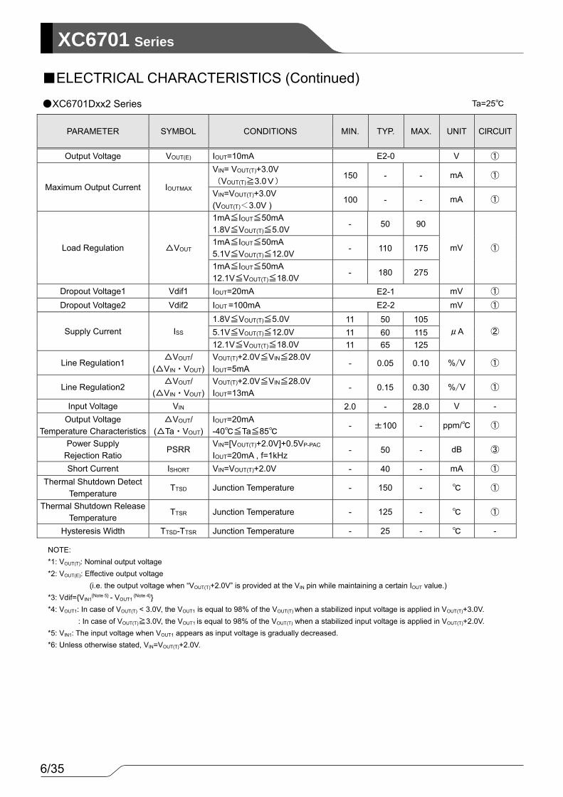
●XC6701A/B Series ●XC6701D Series
Circuit ③
Circuit ①
Circuit ②
●XC6701A/B Series ●XC6701D Series
●XC6701A/B Series ●XC6701D Series
■ TEST CIRCUITS
13/35
XC6701Series
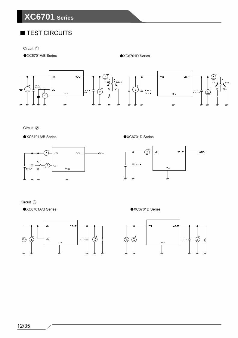
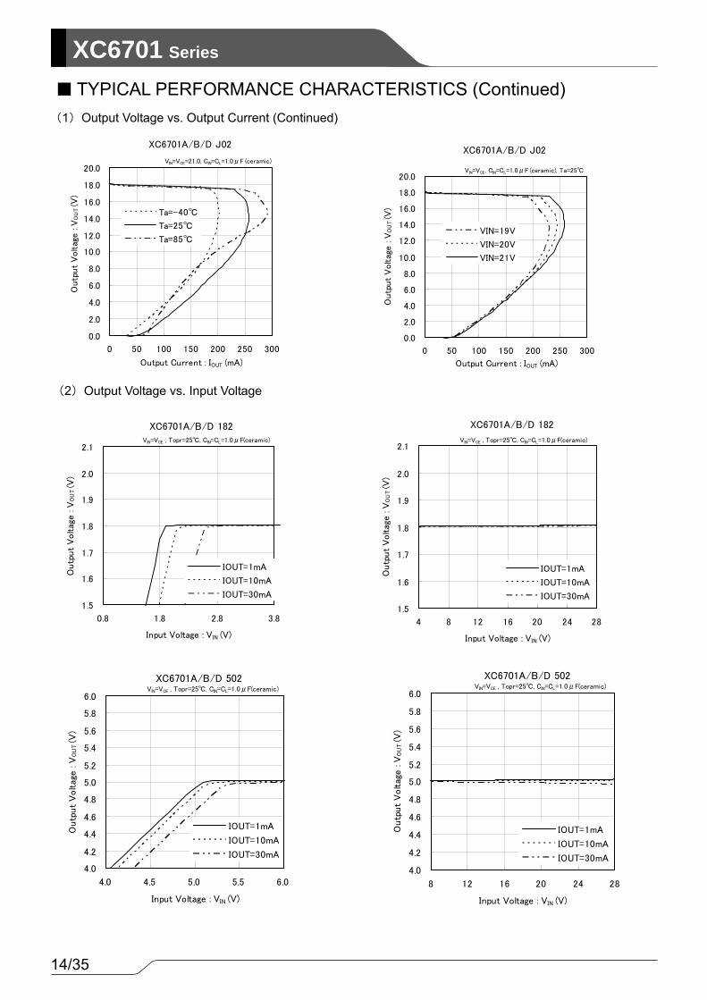
■ TYPICAL PERFORMANCE CHARACTERISTICS
(1) Output Voltage vs. Output Current
XC6701A/B/D 182
0.0
0.2
0.4
0.6
0.8
1.0
1.2
1.4
1.6
1.8
2.0
0 50 100 150 200 250 300
Output Current : IOUT (mA)
Outp
ut
Voltag
e :
VO
UT (V
)
VIN=2.8V
VIN=3.8V
VIN=4.8V
VIN=VCE, CIN=CL=1.0μF (ceramic), Ta=25℃
XC6701A/B/D 182
0.0
0.2
0.4
0.6
0.8
1.0
1.2
1.4
1.6
1.8
2.0
0 50 100 150 200 250 300
Output Current : IOUT (mA)
Outp
ut
Voltag
e :
VO
UT (V
)
Ta=-40℃
Ta=25℃
Ta=85℃
VIN=VCE=4.8V, CIN=CL=1.0μF (ceramic)
XC6701A/B/D 502
0.0
1.0
2.0
3.0
4.0
5.0
6.0
0 50 100 150 200 250 300
Output Current : IOUT (mA)
Outp
ut
Voltag
e :
VO
UT (V
)
Ta=-40℃
Ta=25℃
Ta=85℃
VIN=VCE=8.0V, CIN=CL=1.0μF (ceramic)
XC6701A/B/D 502
0.0
1.0
2.0
3.0
4.0
5.0
6.0
0 50 100 150 200 250 300
Output Current : IOUT (mA)
Outp
ut
Voltag
e :
VO
UT (V
)
VIN=6V
VIN=7V
VIN=8V
VIN=VCE, CIN=CL=1.0μF (ceramic), Ta=25℃
XC6701A/B/D C02
0.0
2.0
4.0
6.0
8.0
10.0
12.0
14.0
0 50 100 150 200 250 300
Output Current : IOUT (mA)
Outp
ut
Voltag
e :
VO
UT (V
)
Ta=-40℃
Ta=25℃
Ta=85℃
VIN=VCE=15.0V, CIN=CL=1.0μF (ceramic)
XC6701A/B/D C02
0.0
2.0
4.0
6.0
8.0
10.0
12.0
14.0
0 50 100 150 200 250 300
Output Current : IOUT (mA)
Outp
ut
Voltag
e :
VO
UT (V
)
VIN=13V
VIN=14V
VIN=15V
VIN=VCE, CIN=CL=1.0μF (ceramic), Ta=25℃
14/35
XC6701 Series
■ TYPICAL PERFORMANCE CHARACTERISTICS (Continued) (1) Output Voltage vs. Output Current (Continued)
(2) Output Voltage vs. Input Voltage
XC6701A/B/D J02
0.0
2.0
4.0
6.0
8.0
10.0
12.0
14.0
16.0
18.0
20.0
0 50 100 150 200 250 300
Output Current : IOUT (mA)
Outp
ut
Voltag
e :
VO
UT (V
)
Ta=-40℃
Ta=25℃
Ta=85℃
VIN=VCE=21.0, CIN=CL=1.0μF (ceramic)
XC6701A/B/D J02
0.0
2.0
4.0
6.0
8.0
10.0
12.0
14.0
16.0
18.0
20.0
0 50 100 150 200 250 300
Output Current : IOUT (mA)
Outp
ut
Voltag
e :
VO
UT (V
)
VIN=19V
VIN=20V
VIN=21V
VIN=VCE, CIN=CL=1.0μF (ceramic), Ta=25℃
XC6701A/B/D 182
1.5
1.6
1.7
1.8
1.9
2.0
2.1
0.8 1.8 2.8 3.8
Input Voltage : VIN (V)
Outp
ut
Voltag
e :
VO
UT (V
)
IOUT=1mA
IOUT=10mA
IOUT=30mA
VIN=VCE , Topr=25℃, CIN=CL=1.0μF(ceramic)
XC6701A/B/D 182
1.5
1.6
1.7
1.8
1.9
2.0
2.1
4 8 12 16 20 24 28
Input Voltage : VIN (V)
Outp
ut
Voltag
e :
VO
UT (V
)
IOUT=1mA
IOUT=10mA
IOUT=30mA
VIN=VCE , Topr=25℃, CIN=CL=1.0μF(ceramic)
XC6701A/B/D 502
4.0
4.2
4.4
4.6
4.8
5.0
5.2
5.4
5.6
5.8
6.0
4.0 4.5 5.0 5.5 6.0
Input Voltage : VIN (V)
Outp
ut
Voltag
e :
VO
UT (V
)
IOUT=1mA
IOUT=10mA
IOUT=30mA
VIN=VCE , Topr=25℃, CIN=CL=1.0μF(ceramic)
XC6701A/B/D 502
4.0
4.2
4.4
4.6
4.8
5.0
5.2
5.4
5.6
5.8
6.0
8 12 16 20 24 28
Input Voltage : VIN (V)
Outp
ut
Voltag
e :
VO
UT (V
)
IOUT=1mA
IOUT=10mA
IOUT=30mA
VIN=VCE , Topr=25℃, CIN=CL=1.0μF(ceramic)

15/35
XC6701Series
(3) Dropout Voltage vs. Output Current
■ TYPICAL PERFORMANCE CHARACTERISTICS (Continued) (2) Output Voltage vs. Input Voltage (Continued)
XC6701A//D 182
0.0
0.5
1.0
1.5
2.0
2.5
3.0
3.5
4.0
0 25 50 75 100 125 150
Output Current : IOUT (mA)
Dro
pout
Voltag
e : V
DIF (
V)
Ta=85℃
Ta=25℃
Ta=-40℃
VIN=VCE, CIN=CL=1.0μF(ceramic)
XC6701A/B/D 502
0.0
0.5
1.0
1.5
2.0
2.5
3.0
3.5
4.0
0 25 50 75 100 125 150
Output Current : IOUT (mA)
Dro
pout
Voltag
e : V
DIF (
V)
Ta=85℃
Ta=25℃
Ta=-40℃
VIN=VCE, CIN=CL=1.0μF(ceramic)
XC6701A/B/D C02
9.0
10.0
11.0
12.0
13.0
14.0
15.0
10 11 12 13 14
Input Voltage : VIN (V)
Outp
ut
Voltag
e :
VO
UT (V
)
IOUT=1mA
IOUT=10mA
IOUT=30mA
VIN=VCE , Topr=25℃, CIN=CL=1.0μF(ceramic)
XC6701A/B/D C02
9.0
10.0
11.0
12.0
13.0
14.0
15.0
14 16 18 20 22 24 26 28
Input Voltage : VIN (V)
Outp
ut
Voltag
e :
VO
UT (V
)
IOUT=1mA
IOUT=10mA
IOUT=30mA
VIN=VCE , Topr=25℃, CIN=CL=1.0μF(ceramic)
XC6701A/B/D J02
15.0
16.0
17.0
18.0
19.0
20.0
21.0
16 17 18 19 20
Input Voltage : VIN (V)
Outp
ut
Voltag
e :
VO
UT (V
)
IOUT=1mA
IOUT=10mA
IOUT=30mA
VIN=VCE , Topr=25℃, CIN=CL=1.0μF(ceramic)
XC6701A/B/D J02
15.0
16.0
17.0
18.0
19.0
20.0
21.0
20 22 24 26 28
Input Voltage : VIN (V)
Outp
ut
Voltag
e :
VO
UT (V
)
IOUT=1mA
IOUT=10mA
IOUT=30mA
VIN=VCE , Topr=25℃, CIN=CL=1.0μF(ceramic)

16/35
XC6701 Series
■ TYPICAL PERFORMANCE CHARACTERISTICS (Continued) (3) Dropout Voltage vs. Output Current (Continued)
(4) Supply Current vs. Input Voltage
XC6701A/B/D J02
0.0
0.5
1.0
1.5
2.0
2.5
3.0
3.5
4.0
0 25 50 75 100 125 150
Output Current : IOUT (mA)D
ropo
ut
Voltag
e : V
DIF (
V)
Ta=85℃
Ta=25℃
Ta=-40℃
VIN=VCE, CIN=CL=1.0μF(ceramic)
XC6701A/B/D C02
0.0
0.5
1.0
1.5
2.0
2.5
3.0
3.5
4.0
0 25 50 75 100 125 150
Output Current : IOUT (mA)
Dro
pout
Voltag
e : V
DIF (
V)
Ta=85℃
Ta=25℃
Ta=-40℃
VIN=VCE, CIN=CL=1.0μ
F( i )
XC6701A/B/D 182
0
10
20
30
40
50
60
70
0 4 8 12 16 20 24 28
Input Voltage : VIN (V)
Supp
ly C
urr
ent
: I S
S (
uA
)
Ta=85℃
Ta=25℃
Ta=-40℃
XC6701A/B/D 502
0
10
20
30
40
50
60
70
0 4 8 12 16 20 24 28
Input Voltage : VIN (V)
Supp
ly C
urr
ent
: I S
S (
uA
)
Ta=85℃
Ta=25℃
Ta=-40℃
XC6701A/B/D 182
0
10
20
30
40
50
60
70
-40 -20 0 20 40 60 80 100
Ambient Temperature : Ta (℃)
Supp
ly C
urr
ent
: I S
S (
uA
)
VIN=3.8V
XC6701A/B/D 502
0
10
20
30
40
50
60
70
-40 -20 0 20 40 60 80 100
Ambient Temperature : Ta (℃)
Supp
ly C
urr
ent
: I S
S (
uA
)
VIN=7.0V

17/35
XC6701Series
(4) Supply Current vs. Input Voltage (Continued)
■ TYPICAL PERFORMANCE CHARACTERISTICS (Continued)
(5) Output Voltage vs. Ambient Temperature
XC6701A/B/D C02
0
10
20
30
40
50
60
70
0 4 8 12 16 20 24 28
Input Voltage : VIN (V)
Supply
Curr
ent
: I S
S (
uA
)
Ta=85℃
Ta=25℃
Ta=-40℃
XC6701A/B/D J02
0
10
20
30
40
50
60
70
0 4 8 12 16 20 24 28
Input Voltage : VIN (V)
Supp
ly C
urr
ent
: I S
S (
uA
)
Ta=85℃
Ta=25℃
Ta=-40℃
XC6701A/B/D C02
0
10
20
30
40
50
60
70
-40 -20 0 20 40 60 80 100
Ambient Temperature : Ta (℃)
Supp
ly C
urr
ent
: I S
S (
uA
)
VIN=14.0V
XC6701A/B/D J02
0
10
20
30
40
50
60
70
-40 -20 0 20 40 60 80 100
Ambient Temperature : Ta (℃)
Supp
ly C
urr
ent
: I S
S (
uA
)
VIN=20.0V
XC6701A/B/D 182
1.60
1.65
1.70
1.75
1.80
1.85
1.90
1.95
2.00
-50 -25 0 25 50 75 100Ambient Temperature : Ta (℃)
Outp
ut
Voltag
e : V
OU
T (
V)
IOUT=1mA
IOUT=10mA
IOUT=20mA
VIN=VCE, CIN=CL=1.0μF(ceramic)
XC6701A/B/D 502
4.80
4.85
4.90
4.95
5.00
5.05
5.10
5.15
5.20
-50 -25 0 25 50 75 100Ambient Temperature : Ta (℃)
Outp
ut
Voltag
e : V
OU
T (
V)
IOUT=1mA
IOUT=10mA
IOUT=20mA
VIN=VCE, CIN=CL=1.0μF(ceramic)

18/35
XC6701 Series
XC6701A/B/D 332
1.3
2.3
3.3
4.3
5.3
6.3
7.3
Time (1ms/div)
Inpu
t V
oltag
e: V
IN (V
)
3.26
3.28
3.30
3.32
3.34
3.36
3.38
Outp
ut
Voltag
e: V
OU
T
(V)
Input Voltage
IOUT=1mA, tr=tf=5μs
CL=1.0μF (ceramic), Ta=25℃
Output Voltage
XC6701A/B/D 332
1.3
2.3
3.3
4.3
5.3
6.3
7.3
Time (1ms/div)
Inpu
t V
oltag
e: V
IN (V
)
3.26
3.28
3.30
3.32
3.34
3.36
3.38
Outp
ut
Voltag
e: V
OU
T
(V)
Input Voltage
IOUT=30mA, tr=tf=5μs
CL=1.0μF (ceramic), Ta=25℃
Output Voltage
XC6701A/B/D 502
3
4
5
6
7
8
9
Time (1ms/div)
Inpu
t V
oltag
e: V
IN (V
)
4.96
4.98
5.00
5.02
5.04
5.06
5.08
Outp
ut
Voltag
e: V
OU
T
(V)
Input Voltage
IOUT=1mA, tr=tf=5μs
CL=1.0μF (ceramic), Ta=25℃
Output Voltage
XC6701A/B/D 502
3
4
5
6
7
8
9
Time (1ms/div)
Inpu
t V
oltag
e: V
IN (V
)
4.96
4.98
5.00
5.02
5.04
5.06
5.08
Outp
ut
Voltag
e: V
OU
T
(V)
Input Voltage
IOUT=30mA, tr=tf=5μs
CL=1.0μF (ceramic), Ta=25℃
Output Voltage
■ TYPICAL PERFORMANCE CHARACTERISTICS (Continued) (5)Output Voltage vs. Ambient Temperature (Continued)
(6) Input Transient Response
XC6701A/B/D C02
11.5
11.6
11.7
11.8
11.9
12.0
12.1
12.2
12.3
12.4
12.5
-50 -25 0 25 50 75 100Ambient Temperature : Ta (℃)
Outp
ut
Voltag
e : V
OU
T (
V)
IOUT=1mA
IOUT=10mA
IOUT=20mA
VIN=VCE, CIN=CL=1.0μF(ceramic)
XC6701A/B/D J02
17.0
17.2
17.4
17.6
17.8
18.0
18.2
18.4
18.6
18.8
19.0
-50 -25 0 25 50 75 100Ambient Temperature : Ta (℃)
Outp
ut
Voltag
e : V
OU
T (
V)
IOUT=1mA
IOUT=10mA
IOUT=20mA
VIN=VCE, CIN=CL=1.0μF(ceramic)

19/35
XC6701Series
■ TYPICAL PERFORMANCE CHARACTERISTICS (Continued)
(6) Input Transient Response (Continued)
XC6701A/B/D C02
10
11
12
13
14
15
16
Time (1ms/div)
Inpu
t V
oltag
e: V
IN (V
)
11.96
11.98
12.00
12.02
12.04
12.06
12.08
Outp
ut
Voltag
e: V
OU
T
(V)
Input Voltage
IOUT=1mA, tr=tf=5μs
CL=1.0μF (ceramic), Ta=25℃
Output Voltage
XC6701A/B/D C02
10
11
12
13
14
15
16
Time (1ms/div)
Inpu
t V
oltag
e: V
IN (V
)
11.96
11.98
12.00
12.02
12.04
12.06
12.08
Outp
ut
Voltag
e: V
OU
T
(V)
Input Voltage
IOUT=30mA, tr=tf=5μs
CL=1.0μF (ceramic), Ta=25℃
Output Voltage
XC6701A/B/D J02
16
17
18
19
20
21
22
Time (1ms/div)
Inpu
t V
oltag
e: V
IN (V
)
17.94
17.97
18.00
18.03
18.06
18.09
18.12
Outp
ut
Voltag
e: V
OU
T
(V)
Input Voltage
IOUT=1mA, tr=tf=5μs
CL=1.0μF (ceramic), Ta=25℃
Output Voltage
XC6701A/B/D J02
16
17
18
19
20
21
22
Time (1ms/div)
Inpu
t V
oltag
e: V
IN (V
)
17.94
17.97
18.00
18.03
18.06
18.09
18.12
Outp
ut
Voltag
e: V
OU
T
(V)
Input Voltage
IOUT=30mA, tr=tf=5μs
CL=1.0μF (ceramic), Ta=25℃
Output Voltage
XC6701A/B/D 332
2.6
2.7
2.8
2.9
3.0
3.1
3.2
3.3
3.4
3.5
3.6
Time (1ms/div)
Outp
ut
Voltag
e: V
OU
T (V
)
0
30
60
90
120
150
Outp
ut
Curr
ent: I
OU
T (
mA
)
Output Current
VIN=5.3V, tr=tf=5μs
CIN=CL=1.0μF (ceramic), Ta=25℃
Output Voltage
XC6701A/B/D 502
4.4
4.5
4.6
4.7
4.8
4.9
5.0
5.1
5.2
5.3
5.4
Time (1ms/div)
Outp
ut
Voltag
e: V
OU
T (V
)
0
30
60
90
120
150
Outp
ut
Curr
ent: I
OU
T (
mA
)
Output Current
VIN=7.0V, tr=tf=5μs
CIN=CL=1.0μF (ceramic), Ta=25℃
Output Voltage
(7) Load Transient Response

20/35
XC6701 Series
■ TYPICAL PERFORMANCE CHARACTERISTICS (Continued) (7) Load Transient Response (Continued)
(8) Rising Response Time
XC6701A/B/D C02
10.6
10.8
11.0
11.2
11.4
11.6
11.8
12.0
12.2
12.4
12.6
Time (1ms/div)
Outp
ut
Voltag
e: V
OU
T (V
)
0
30
60
90
120
150
Outp
ut
Curr
ent: I
OU
T (
mA
)Output Current
VIN=14.0V, tr=tf=5μs
CIN=CL=1.0μF (ceramic), Ta=25℃
Output Voltage
XC6701A/B/D J02
16.6
16.8
17.0
17.2
17.4
17.6
17.8
18.0
18.2
18.4
18.6
Time (1ms/div)
Outp
ut
Voltag
e: V
OU
T (V
)
0
30
60
90
120
150
Outp
ut
Curr
ent: I
OU
T (
mA
)
Output Current
VIN=20.0V, tr=tf=5μs
CIN=CL=1.0μF (ceramic), Ta=25℃
Output Voltage
XC6701A/B 332
-8
-6
-4
-2
0
2
4
6
8
Time (1ms/div)
Inpu
t V
oltag
e: V
IN (V
)
0
1
2
3
4
5
6
7
8
Outp
ut
Voltag
e: V
OU
T (V
)
VIN=5.3V, tr=5μs
IOUT=30mA, CL=1μF (ceramic), Ta=25℃
Input Voltage
Output Voltage
XC6701A/B 332
-8
-6
-4
-2
0
2
4
6
8
Time (1ms/div)
Inpu
t V
oltag
e: V
IN (V
)
0
1
2
3
4
5
6
7
8
Outp
ut
Voltag
e: V
OU
T (V
)
VIN=5.3V, tr=5μs
IOUT=1mA, CL=1μF (ceramic), Ta=25℃
Input Voltage
Output Voltage
XC6701A/B 502
-8
-6
-4
-2
0
2
4
6
8
Time (1ms/div)
Inpu
t V
oltag
e: V
IN (V
)
0
1
2
3
4
5
6
7
8
Outp
ut
Voltag
e: V
OU
T (V
)
VIN=7.0V, tr=5μs
IOUT=30mA, CL=1μF (ceramic), Ta=25℃
Input Voltage
Output Voltage
XC6701A/B 502
-8
-6
-4
-2
0
2
4
6
8
Time (1ms/div)
Inpu
t V
oltag
e: V
IN (V
)
0
1
2
3
4
5
6
7
8
Outp
ut
Voltag
e: V
OU
T (V
)
VIN=7.0V, tr=5μs
IOUT=1mA, CL=1μF (ceramic), Ta=25℃
Input Voltage
Output Voltage

21/35
XC6701Series
(8) Rising Response Time (Continued)
■ TYPICAL PERFORMANCE CHARACTERISTICS (Continued)
(9) CE Rising Response Time
XC6701A/B C02
-15
-10
-5
0
5
10
15
Time (1ms/div)
Inpu
t V
oltag
e: V
IN (
V)
0
3
6
9
12
15
18
Outp
ut
Voltag
e: V
OU
T (
V)
VIN=14.0V, tr=5μs
IOUT=1mA, CL=1μF (ceramic), Ta=25℃
Input Voltage
Output Voltage
XC6701A/B C02
-15
-10
-5
0
5
10
15
Time (1ms/div)
Inpu
t V
oltag
e: V
IN (
V)
0
3
6
9
12
15
18
Outp
ut
Voltag
e: V
OU
T (
V)
VIN=14.0V, tr=5μs
IOUT=30mA, CL=1μF (ceramic), Ta=25℃
Input Voltage
Output Voltage
XC6701A/B J02
-20
-16
-12
-8
-4
0
4
8
12
16
20
Time (1ms/div)
Inpu
t V
oltag
e: V
IN (
V)
0
2
4
6
8
10
12
14
16
18
20
Outp
ut
Voltag
e: V
OU
T (
V)
VIN=20.0V, tr=5μs
IOUT=1mA, CL=1μF (ceramic), Ta=25℃
Input Voltage
Output Voltage
XC6701A/B J02
-20
-16
-12
-8
-4
0
4
8
12
16
20
Time (1ms/div)
Inpu
t V
oltag
e: V
IN (
V)
0
2
4
6
8
10
12
14
16
18
20
Outp
ut
Voltag
e: V
OU
T (
V)
VIN=20.0V, tr=5μs
IOUT=30mA, CL=1μF (ceramic), Ta=25℃
Input Voltage
Output Voltage
Output Voltage
XC6701A/B 332
-8
-6
-4
-2
0
2
4
6
8
Time (1ms/div)
CEIn
put
Voltag
e: V
CE (
V)
0
1
2
3
4
5
6
7
8
Outp
ut
Voltag
e: V
OU
T (
V)
VIN=5.3V, tr=5μs
IOUT=1mA, CL=1μF (ceramic), Ta=25℃
CE Input Voltage
Output Voltage
XC6701A/B 332
-8
-6
-4
-2
0
2
4
6
8
Time (1ms/div)
CEIn
put
Voltag
e: V
CE (
V)
0
1
2
3
4
5
6
7
8
Outp
ut
Voltag
e: V
OU
T (
V)
VIN=5.3V, tr=5μs
IOUT=30mA, CL=1μF (ceramic), Ta=25℃
CE Input Voltage
Output Voltage

22/35
XC6701 Series
■ TYPICAL PERFORMANCE CHARACTERISTICS (Continued) (9) CE Rising Response Time (Continued)
XC6701A/B 502
-8
-6
-4
-2
0
2
4
6
8
Time (1ms/div)
CEIn
put
Voltag
e: V
CE (V
)
0
1
2
3
4
5
6
7
8
Outp
ut
Voltag
e: V
OU
T (
V)
VIN=7.0V, tr=5μs
IOUT=1mA, CL=1μF (ceramic), Ta=25℃
CE Input Voltage
Output Voltage
XC6701A/B 502
-8
-6
-4
-2
0
2
4
6
8
Time (1ms/div)
CEIn
put
Voltag
e: V
CE (
V)
0
1
2
3
4
5
6
7
8
Outp
ut
Voltag
e: V
OU
T (
V)
VIN=7.0V, tr=5μs
IOUT=30mA, CL=1μF (ceramic), Ta=25℃
CE Input Voltage
Output Voltage
XC6701A/B C02
-15
-10
-5
0
5
10
15
Time (1ms/div)
CEIn
put
Voltag
e: V
CE (
V)
0
3
6
9
12
15
18
Outp
ut
Voltag
e: V
OU
T (
V)
VIN=14.0V, tr=5μs
IOUT=1mA, CL=1μF (ceramic), Ta=25℃
CE Input Voltage
Output Voltage
XC6701A/B C02
-15
-10
-5
0
5
10
15
Time (1ms/div)
CEIn
put
Voltag
e: V
CE (
V)
0
3
6
9
12
15
18
Outp
ut
Voltag
e: V
OU
T (
V)
VIN=14.0V, tr=5μs
IOUT=30mA, CL=1μF (ceramic), Ta=25℃
CE Input Voltage
Output Voltage
XC6701A/B J02
-20
-16
-12
-8
-4
0
4
8
12
16
20
Time (1ms/div)
CEIn
put
Voltag
e: V
CE (
V)
0
2
4
6
8
10
12
14
16
18
20
Outp
ut
Voltag
e: V
OU
T (
V)
VIN=20.0V, tr=5μs
IOUT=1mA, CL=1μF (ceramic), Ta=25℃
CE Input Voltage
Output Voltage
XC6701A/B J02
-20
-16
-12
-8
-4
0
4
8
12
16
20
Time (1ms/div)
CEIn
put
Voltag
e: V
CE (
V)
0
2
4
6
8
10
12
14
16
18
20
Outp
ut
Voltag
e: V
OU
T (
V)
VIN=20.0V, tr=5μs
IOUT=30mA, CL=1μF (ceramic), Ta=25℃
CE Input Voltage
Output Voltage

23/35
XC6701Series
■ TYPICAL PERFORMANCE CHARACTERISTICS (Continued) (10) Ripple Rejection Rate
XC6701A/B/D 332
0
10
20
30
40
50
60
70
80
90
0.01 0.1 1 10 100
Ripple Frequency: f (kHz)
Rip
ple
Reje
ction R
ate: P
SR
R (
dB)
VIN=VCE=5.3Vdc+0.5Vp-p, IOUT=1mA
CL=1μF(ceramic),Topr=25℃
XC6701A/B/D 332
0
10
20
30
40
50
60
70
80
90
0.01 0.1 1 10 100
Ripple Frequency: f (kHz)
Rip
ple
Reje
ction R
ate: P
SR
R (
dB)
VIN=VCE=5.3Vdc+0.5Vp-p, IOUT=30mA
CL=1μF(ceramic),Topr=25℃
XC6701A/B/D 502
0
10
20
30
40
50
60
70
80
90
0.01 0.1 1 10 100
Ripple Frequency: f (kHz)
Rip
ple R
eje
ction R
ate: P
SR
R (
dB
)
VIN=VCE=7.0Vdc+0.5Vp-p, IOUT=1mA
CL=1μF(ceramic),Topr=25℃
XC6701A/B/D 502
0
10
20
30
40
50
60
70
80
90
0.01 0.1 1 10 100
Ripple Frequency: f (kHz)
Rip
ple R
eje
ction R
ate: P
SR
R (
dB
)
VIN=VCE=7.0Vdc+0.5Vp-p, IOUT=30mA
CL=1μF(ceramic),Topr=25℃
XC6701A/B/D C02
0
10
20
30
40
50
60
70
80
90
0.01 0.1 1 10 100
Ripple Frequency: f (kHz)
Rip
ple R
eje
ction R
ate: P
SR
R (
dB)
VIN=VCE=14.0Vdc+0.5Vp-p, IOUT=1mA
CL=1μF(ceramic),Topr=25℃
XC6701A/B/D C02
0
10
20
30
40
50
60
70
80
90
0.01 0.1 1 10 100
Ripple Frequency: f (kHz)
Rip
ple R
eje
ction R
ate: P
SR
R (
dB)
VIN=VCE=14.0Vdc+0.5Vp-p, IOUT=30mA
CL=1μF(ceramic),Topr=25℃

24/35
XC6701 Series
■ TYPICAL PERFORMANCE CHARACTERISTICS (Continued) (10) Ripple Rejection Rate (Continued)
XC6701A/B/D J02
0
10
20
30
40
50
60
70
80
90
0.01 0.1 1 10 100
Ripple Frequency: f (kHz)
Rip
ple R
eje
ction R
ate: P
SR
R (
dB)
VIN=VCE=14.0Vdc+0.5Vp-p, IOUT=1mA
CL=1μF(ceramic),Topr=25℃
XC6701A/B/D J02
0
10
20
30
40
50
60
70
80
90
0.01 0.1 1 10 100
Ripple Frequency: f (kHz)
Rip
ple R
eje
ction R
ate: P
SR
R (
dB)
VIN=VCE=14.0Vdc+0.5Vp-p, IOUT=30mA
CL=1μF(ceramic),Topr=25℃

25/35
XC6701Series
●SOT-25
●USP-6C
■PACKAGING INFORMATION
●USP-6C Reference Pattern Layout
●USP-6C Reference Metal Mask Design
2.4
2
3 4
5
61
0.45
1.0
0.050.05
2
3 4
5
61
0.45
0.35
2.3
0.35
0.8
0.150.15
Unit :mm
Unit :mm
Unit : mm
Unit : mm
1.8±0.05
(0.50)
(0.1)
1.4±0.05
0.20±0.05
0.30±0.05
0.10±0.05
1pin INDENT
0.05

26/35
XC6701 Series
●SOT-89-5
●SOT-223
●TO-252
■PACKAGING INFORMATION (Continued)
●SOT-89
3.5±0.2
7.0±0.3
1.68+0.12
-0.13
0.91MIN
Unit :mm
Unit :mm
Unit :mm Unit :mm
1.6 +0.15-0.2
4.5±0.1
φ1.0
0.42±0.060.47±0.060.42±0.06
1.5±0.1
0.4+0.03-0.02
1.5±0.1
0.4+0.03-0.02
(1.7)
Φ1.0
1.6+0.15-0.2
4.5±0.1
0.42±0.06 0.42±0.060.47±0.06
1.5±0.1 1.5±0.1
0.4+0.03-0.02
0.4+0.03-0.02
1 2 3
45
0.42±0.06 0.42±0.06 0.42±0.06
2
(1.6)
(1.7)
(2.29) (2.29)
4.94-5.50
BOTTOM VIEW
0.64-0.89
0.64-0.89
0.64-0.89
0.46-0.61
4.32 MIN
6.35-6.75

27/35
XC6701Series
● SOT-25 Power Dissipation Board Mount (Tj max = 125℃)
Board Mount (Tj max = 125℃)
Ambient Temperature
(℃)
Power Dissipation Pd (mW)
Thermal Resistance
(℃/W) 25 600
166.67 85 240
Ambient Temperature
(℃)
Power Dissipation Pd (mW)
Thermal Resistance
(℃/W) 25 600
166.67 105 120
■PACKAGING INFORMATION (Continued)
Power dissipation data for the SOT-25 is shown in this page. The value of power dissipation varies with the mount board conditions. Please use this data as the reference data taken in the following condition.
1. Measurement Condition Condition: Mount on a board Ambient: Natural convection Soldering: Lead (Pb) free Board: Dimensions 40 x 40 mm (1600 mm2 in one side)
Copper (Cu) traces occupy 50% of the board area In top and back faces Package heat-sink is tied to the copper traces (Board of SOT-26 is used.)
Material: Glass Epoxy (FR-4) Thickness: 1.6 mm Through-hole: 4 x 0.8 Diameter
Evaluation Board (Unit: mm)
2. Power Dissipation vs. Ambient Temperature (85℃) 評価基板レイアウト(単位:mm)Evaluation Board (Unit: mm)
Pd vs Ta
0
100
200
300
400
500
600
700
25 45 65 85 105 125
Ambient Temperature Ta(℃)
Pow
er D
issi
pat
ion P
d(m
W)
3. Power Dissipation vs. Ambient Temperature (105℃)
Pd vs Ta
0
100
200
300
400
500
600
700
25 45 65 85 105 125
Ambient Temparature Ta(℃)
Pow
er
Dis
sipa
tion P
d(m
W)

28/35
XC6701 Series
● SOT-89-5 Power Dissipation
Board Mount (Tj max = 125℃)
Ambient Temperature
(℃)
Power Dissipation Pd(mW)
Thermal Resistance
(℃/W)
25 1300 76.92
85 520 Board Mount (Tj max = 125℃)
Ambient Temperature
(℃)
Power Dissipation Pd(mW)
Thermal Resistance
(℃/W)
25 1300 76.92
105 260
て
■PACKAGING INFORMATION (Continued)
Power dissipation data for the SOT-89-5 is shown in this page. The value of power dissipation varies with the mount board conditions. Please use this data as the reference data taken in the following condition.
1. Measurement Condition Condition: Mount on a board Ambient: Natural convection Soldering: Lead (Pb) free Board: Dimensions 40 x 40 mm (1600 mm2 in one side)
Copper (Cu) traces occupy 50% of the board area In top and back faces Package heat-sink is tied to the copper traces
Material: Glass Epoxy (FR-4) Thickness: 1.6 mm Through-hole: 5 x 0.8 Diameter
Evaluation Board (Unit: mm) 2. Power Dissipation vs. Ambient Temperature (85℃)
Pd-Ta特性グラフ
0
200
400
600
800
1000
1200
1400
25 45 65 85 105 125
周辺温度Ta(℃)
許容
損失
Pd(m
W)
Pd vs. Ta
Ambient Temperature Ta (℃)
Pow
er D
issi
patio
n P
d (m
W)
3. Power Dissipation vs. Ambient Temperature (105℃) Pd vs. Ta
0
200
400
600
800
1000
1200
1400
25 45 65 85 105 125
Ambient Temperature Ta (℃)
Pow
er
Dis
sipa
tion P
d (m
W)

29/35
XC6701Series
● USP-6C Power Dissipation
Board Mount (Tj max = 125℃)
Ambient Temperature
(℃)
Power Dissipation Pd(mW)
Thermal Resistance
(℃/W)
25 1000 100.00
85 400 Board Mount (Tj max = 125℃)
Ambient Temperature
(℃)
Power Dissipation Pd(mW)
Thermal Resistance
(℃/W)
25 1000 100.00
105 200
て
Power dissipation data for the USP-6C is shown in this page. The value of power dissipation varies with the mount board conditions. Please use this data as the reference data taken in the following condition.
1. Measurement Condition Condition: Mount on a board Ambient: Natural convection Soldering: Lead (Pb) free Board: Dimensions 40 x 40 mm (1600 mm2 in one side)
Copper (Cu) traces occupy 50% of the board area In top and back faces Package heat-sink is tied to the copper traces
Material: Glass Epoxy (FR-4) Thickness: 1.6 mm Through-hole: 4 x 0.8 Diameter
Evaluation Board (Unit: mm) 2. Power Dissipation vs. Ambient Temperature (85℃)
Pd-Ta特性グラフ
0
200
400
600
800
1000
1200
25 45 65 85 105 125
周辺温度Ta(℃)
許容
損失
Pd(
mW
)
Pd vs. Ta
Ambient Temperature Ta (℃)
Pow
er D
issi
patio
n P
d (m
W)
■PACKAGING INFORMATION (Continued)
3. Power Dissipation vs. Ambient Temperature (105℃)
Pd-Ta特性グラフ
0
200
400
600
800
1000
1200
25 45 65 85 105 125
周囲温度Ta(℃)
許容
損失
Pd(
mW
)
Pd vs. Ta
Ambient Temperature Ta (℃)

30/35
XC6701 Series
● SOT-223 Power Dissipation
Board Mount (Tj max = 125℃)
Ambient Temperature(℃) Power Dissipation Pd(mW) Thermal Resistance (℃/W)
25 1500 66.67
85 600
Pd-Ta特性グラフ
0200400600800
1000120014001600
25 45 65 85 105 125
周辺温度Ta(℃)
許容
損失
Pd(
mW
)
Power dissipation data for the SOT-223 is shown in this page. The value of power dissipation varies with the mount board conditions. Please use this data as the reference data taken in the following condition.
1. Measurement Condition Condition: Mount on a board Ambient: Natural convection Soldering: Lead (Pb) free Board: Dimensions 40 x 40 mm (1600 mm2 in one side)
Copper (Cu) traces occupy 50% of the board area In top and back faces Package heat-sink is tied to the copper traces
Material: Glass Epoxy (FR-4) Thickness: 1.6 mm Through-hole: 4 x 0.8 Diameter
Evaluation Board (Unit: mm) 2. Power Dissipation vs. Ambient Temperature
Pd vs. Ta
Ambient Temperature Ta (℃)
Pow
er D
issi
patio
n P
d (m
W)
■PACKAGING INFORMATION (Continued)

31/35
XC6701Series
● TO-252 Power Dissipation Power dissipation data for the TO-252 is shown in this page. The value of power dissipation varies with the mount board conditions. Please use this data as the reference data taken in the following condition.
Ambient Temperature(℃) Power Dissipation Pd(mW) Thermal Resistance (℃/W)
25 1800 55.56
85 720
Evaluation Board (Unit: mm)
2. Power Dissipation vs. Ambient Temperature
1. Measurement Condition Condition: Mount on a board Ambient: Natural convection Soldering: Lead (Pb) free Board: Dimensions 40 x 40 mm (1600 mm2 in one side)
Copper (Cu) traces occupy 50% of the board area In top and back faces Package heat-sink is tied to the copper traces
Material: Glass Epoxy (FR-4) Thickness: 1.6 mm Through-hole: 4 x 0.8 Diameter
Pd vs Ta
0
200
400
600
800
1000
1200
1400
1600
18002000
25 45 65 85 105 125
Ambient Temperature Ta(℃)
Pow
er
Dis
sipation P
d(m
W)
■PACKAGING INFORMATION (Continued)

32/35
XC6701 Series
● SOT-89 Power Dissipation Power dissipation data for the SOT-89 is shown in this page. The value of power dissipation varies with the mount board conditions. Please use this data as the reference data taken in the following condition.
Ambient Temperature(℃) Power Dissipation Pd(mW) Thermal Resistance (℃/W)
25 1000 100.00
85 400
■PACKAGING INFORMATION (Continued)
1. Measurement Condition Condition: Mount on a board Ambient: Natural convection Soldering: Lead (Pb) free Board: Dimensions 40 x 40 mm (1600 mm2 in one side)
Copper (Cu) traces occupy 50% of the board area In top and back faces Package heat-sink is tied to the copper traces
Material: Glass Epoxy (FR-4) Thickness: 1.6 mm Through-hole: 4 x 0.8 Diameter
Evaluation Board (Unit: mm)
2. Power Dissipation vs. Ambient Temperature
Pd vs Ta
0
200
400
600
800
1000
1200
25 45 65 85 105 125
Ambient Temperature Ta(℃)
Pow
er
Dis
sipation P
d(m
W)

33/35
XC6701Series
MARK PRODUCT SERIES
8 XC6701******
MARK TYPE OUTPUT
VOLTAGE (V) PRODUCT SERIES
0
A/B
1.8~3.0
XC6701 A/B*****
1 3.1~6.0
2 6.1~9.0
3 9.1~12.0
A 12.1~15.0
B 15.1~18.0
4
D
1.8~3.0
XC6701D*****
5 3.1~6.0
6 6.1~9.0
7 9.1~12.0
C 12.1~15.0
D 15.1~18.0
■MARKING RULE
① represents product series
1
② ③ ④ ⑤
2 3
①
1 2 3
5 4
① ② ③ ④ ⑤
5 2 4
1 2 3
⑤③①
④②
⑤③①
1 2 3
④②
② represents type of regulators and output voltage
SOT-25
SOT-89
SOT-89-5
SOT-223
(mark header:①~③) *Mark header does not change with a lot.

34/35
XC6701 Series
MARK OUTPUT VOLTAGE(V)
0 - 3.1 6.1 9.1 12.1 15.1
1 - 3.2 6.2 9.2 12.2 15.2
2 - 3.3 6.3 9.3 12.3 15.3
3 - 3.4 6.4 9.4 12.4 15.4
4 - 3.5 6.5 9.5 12.5 15.5
5 - 3.6 6.6 9.6 12.6 15.6
6 - 3.7 6.7 9.7 12.7 15.7
7 - 3.8 6.8 9.8 12.8 15.8
8 - 3.9 6.9 9.9 12.9 15.9
9 - 4.0 7.0 10.0 13.0 16.0
A - 4.1 7.1 10.1 13.1 16.1
B - 4.2 7.2 10.2 13.2 16.2
C - 4.3 7.3 10.3 13.3 16.3
D - 4.4 7.4 10.4 13.4 16.4
E - 4.5 7.5 10.5 13.5 16.5
F - 4.6 7.6 10.6 13.6 16.6
H - 4.7 7.7 10.7 13.7 16.7
K 1.8 4.8 7.8 10.8 13.8 16.8
L 1.9 4.9 7.9 10.9 13.9 16.9
M 2.0 5.0 8.0 11.0 14.0 17.0
N 2.1 5.1 8.1 11.1 14.1 17.1
P 2.2 5.2 8.2 11.2 14.2 17.2
R 2.3 5.3 8.3 11.3 14.3 17.3
S 2.4 5.4 8.4 11.4 14.4 17.4
T 2.5 5.5 8.5 11.5 14.5 17.5
U 2.6 5.6 8.6 11.6 14.6 17.6
V 2.7 5.7 8.7 11.7 14.7 17.7
X 2.8 5.8 8.8 11.8 14.8 17.8
Y 2.9 5.9 8.9 11.9 14.9 17.9
Z 3.0 6.0 9.0 12.0 15.0 18.0
③ represents output voltage ④
⑤
②③
①1
2
3
6
5
4
1 3
2
① ② ③
⑤④
TO-252
USP-6C
■MARKING RULE (Continued)
④⑤ represents production lot number 01, …, 09, 10, 11, …, 99, 0A, …, 0Z, 1A, …, 9Z, A0, …, Z9, AA, …, ZZ repeated. (G, I, J, O, Q, W excluded) *No character inversion used.

35/35
XC6701Series
1. The product and product specifications contained herein are subject to change without notice to improve performance characteristics. Consult us, or our representatives before use, to confirm that the information in this datasheet is up to date.
2. The information in this datasheet is intended to illustrate the operation and characteristics of our
products. We neither make warranties or representations with respect to the accuracy or completeness of the information contained in this datasheet nor grant any license to any intellectual property rights of ours or any third party concerning with the information in this datasheet.
3. Applicable export control laws and regulations should be complied and the procedures required by
such laws and regulations should also be followed, when the product or any information contained in this datasheet is exported.
4. The product is neither intended nor warranted for use in equipment of systems which require
extremely high levels of quality and/or reliability and/or a malfunction or failure which may cause loss of human life, bodily injury, serious property damage including but not limited to devices or equipment used in 1) nuclear facilities, 2) aerospace industry, 3) medical facilities, 4) automobile industry and other transportation industry and 5) safety devices and safety equipment to control combustions and explosions. Do not use the product for the above use unless agreed by us in writing in advance.
5. Although we make continuous efforts to improve the quality and reliability of our products;
nevertheless Semiconductors are likely to fail with a certain probability. So in order to prevent personal injury and/or property damage resulting from such failure, customers are required to incorporate adequate safety measures in their designs, such as system fail safes, redundancy and fire prevention features.
6. Our products are not designed to be Radiation-resistant.
7. Please use the product listed in this datasheet within the specified ranges.
8. We assume no responsibility for damage or loss due to abnormal use.
9. All rights reserved. No part of this datasheet may be copied or reproduced unless agreed by Torex
Semiconductor Ltd in writing in advance.
TOREX SEMICONDUCTOR LTD.