XC4000 Series Field Programmable Gate Arrays...
176
September 18, 1996 (Version 1.04) 4-5 XC4000-Series Features Note: XC4000-Series devices described in this data sheet include the XC4000E, XC4000EX, XC4000L, and XC4000XL. This information does not apply to the older Xilinx families: XC4000, XC4000A, XC4000D or XC4000H. For information on these devices, see the Xilinx W EB LINX at http://www.xilinx.com. • Third Generation Field-Programmable Gate Arrays - Select-RAM TM memory: on-chip ultra-fast RAM with - synchronous write option - dual-port RAM option - Fully PCI compliant (speed grades -3 and faster) - Abundant flip-flops - Flexible function generators - Dedicated high-speed carry logic - Wide edge decoders on each edge - Hierarchy of interconnect lines - Internal 3-state bus capability - 8 global low-skew clock or signal distribution networks • System Performance to 66 MHz • Flexible Array Architecture • Systems-Oriented Features - IEEE 1149.1-compatible boundary scan logic support - Individually programmable output slew rate - Programmable input pull-up or pull-down resistors - 12-mA sink current per XC4000E output (4 mA per XC4000L output) • Configured by Loading Binary File - Unlimited reprogrammability • Readback Capability • Backward Compatible with XC4000 Devices • XACT step Development System runs on '386/'486/ Pentium-type PC, Sun-4, and Hewlett-Packard 700 series - Interfaces to popular design environments - Fully automatic mapping, placement and routing - Interactive design editor for design optimization - RAM/ROM compiler Low-Voltage Versions Available • Low-Voltage Devices Function at 3.0 - 3.6 Volts • XC4000L: Low-Voltage Versions of XC4000E devices • XC4000XL: Low-Voltage Versions of XC4000EX devices Additional XC4000EX/XL Features • Highest Capacity — Over 130,000 Usable Gates • Additional Routing Over XC4000E - almost twice the routing capacity for high-density designs • Buffered Interconnect for Maximum Speed • New Latch Capability in Configurable Logic Blocks • Improved VersaRing TM I/O Interconnect for Better Fixed Pinout Flexibility • Flexible New High-Speed Clock Network - 8 additional Early Buffers for shorter clock delays - 4 additional FastCLK TM buffers for fastest clock input - Virtually unlimited number of clock signals • Optional Multiplexer or 2-input Function Generator on Device Outputs • High-Speed Parallel Express TM Configuration Mode • Improved I/O Setup and Clock-to-Output with FastCLK and Global Early Buffers • 4 Additional Address Bits in Master Parallel Configuration Mode Introduction XC4000-Series high-performance, high-capacity Field Pro- grammable Gate Arrays (FPGAs) provide the benefits of custom CMOS VLSI, while avoiding the initial cost, long development cycle, and inherent risk of a conventional masked gate array. The result of eleven years of FPGA design experience and feedback from thousands of customers, these FPGAs com- bine architectural versatility, on-chip Select-RAM memory with edge-triggered and dual-port modes, increased speed, abundant routing resources, and new, sophisticated soft- ware to achieve fully automated implementation of com- plex, high-density, high-performance designs. The XC4000 Series currently has 19 members, as shown in Table 1. XC4000 Series Field Programmable Gate Arrays September 18, 1996 (Version 1.04) Product Specification
Transcript of XC4000 Series Field Programmable Gate Arrays...

XC4000-Series FeaturesNote: XC4000-Series devices described in this data sheetinclude the XC4000E, XC4000EX, XC4000L, andXC4000XL. This information does not apply to the olderXilinx families: XC4000, XC4000A, XC4000D or XC4000H.For information on these devices, see the Xilinx WEBLINXat http://www.xilinx.com.
• Third Generation Field-Programmable Gate Arrays - Select-RAMTM memory: on-chip ultra-fast RAM with
- synchronous write option - dual-port RAM option
- Fully PCI compliant (speed grades -3 and faster) - Abundant flip-flops - Flexible function generators - Dedicated high-speed carry logic - Wide edge decoders on each edge - Hierarchy of interconnect lines - Internal 3-state bus capability - 8 global low-skew clock or signal distribution
networks • System Performance to 66 MHz• Flexible Array Architecture • Systems-Oriented Features
- IEEE 1149.1-compatible boundary scan logic support
- Individually programmable output slew rate - Programmable input pull-up or pull-down resistors - 12-mA sink current per XC4000E output (4 mA per
XC4000L output) • Configured by Loading Binary File
- Unlimited reprogrammability• Readback Capability • Backward Compatible with XC4000 Devices • XACTstep Development System runs on '386/'486/
Pentium-type PC, Sun-4, and Hewlett-Packard 700 series - Interfaces to popular design environments - Fully automatic mapping, placement and routing - Interactive design editor for design optimization - RAM/ROM compiler
Low-Voltage Versions Available• Low-Voltage Devices Function at 3.0 - 3.6 Volts • XC4000L: Low-Voltage Versions of XC4000E devices • XC4000XL: Low-Voltage Versions of XC4000EX
devices
Additional XC4000EX/XL Features• Highest Capacity — Over 130,000 Usable Gates • Additional Routing Over XC4000E
- almost twice the routing capacity for high-density designs
• Buffered Interconnect for Maximum Speed • New Latch Capability in Configurable Logic Blocks • Improved VersaRingTM I/O Interconnect for Better Fixed
Pinout Flexibility • Flexible New High-Speed Clock Network
- 8 additional Early Buffers for shorter clock delays - 4 additional FastCLKTM buffers for fastest clock input- Virtually unlimited number of clock signals
• Optional Multiplexer or 2-input Function Generator on Device Outputs
• High-Speed Parallel ExpressTM Configuration Mode • Improved I/O Setup and Clock-to-Output with FastCLK
and Global Early Buffers • 4 Additional Address Bits in Master Parallel
Configuration Mode
Introduction XC4000-Series high-performance, high-capacity Field Pro-grammable Gate Arrays (FPGAs) provide the benefits ofcustom CMOS VLSI, while avoiding the initial cost, longdevelopment cycle, and inherent risk of a conventionalmasked gate array.
The result of eleven years of FPGA design experience andfeedback from thousands of customers, these FPGAs com-bine architectural versatility, on-chip Select-RAM memorywith edge-triggered and dual-port modes, increased speed,abundant routing resources, and new, sophisticated soft-ware to achieve fully automated implementation of com-plex, high-density, high-performance designs.
The XC4000 Series currently has 19 members, as shownin Table 1.
XC4000 Series Field Programmable Gate Arrays
September 18, 1996 (Version 1.04) Product Specification
September 18, 1996 (Version 1.04) 4-5

XC4000 Series Field Programmable Gate Arrays
* Max values of Typical Gate Range include 20-30% of CLBs used as RAM.
Note: Throughout the functional descriptions in this docu-ment, references to the XC4000E device family include theXC4000L, and references to the XC4000EX device familyinclude the XC4000XL, unless explicitly stated otherwise.References to the XC4000 Series include the XC4000E,XC4000EX, XC4000L, and XC4000XL families. All func-tionality in low-voltage families is the same as in the corre-sponding 5-Volt family, except where numerical referencesare made to timing, power, or current-sinking capability.
DescriptionXC4000-Series devices are implemented with a regular,flexible, programmable architecture of Configurable LogicBlocks (CLBs), interconnected by a powerful hierarchy ofversatile routing resources, and surrounded by a perimeterof programmable Input/Output Blocks (IOBs). They havegenerous routing resources to accommodate the mostcomplex interconnect patterns.
The devices are customized by loading configuration datainto internal memory cells. The FPGA can either activelyread its configuration data from an external serial or byte-parallel PROM (master modes), or the configuration data
can be written into the FPGA from an external device(slave, peripheral and Express modes).
XC4000-Series FPGAs are supported by powerful andsophisticated software, covering every aspect of designfrom schematic or behavioral entry, floorplanning, simula-tion, automatic block placement and routing of intercon-nects, to the creation, downloading, and readback of theconfiguration bit stream.
Because Xilinx FPGAs can be reprogrammed an unlimitednumber of times, they can be used in innovative designswhere hardware is changed dynamically, or where hard-ware must be adapted to different user applications.FPGAs are ideal for shortening design and developmentcycles, and also offer a cost-effective solution for produc-tion rates well beyond 5,000 systems per month. For lowesthigh-volume unit cost, a design can first be implemented inthe XC4000E or XC4000EX, then migrated to one of Xilinx’compatible HardWire mask-programmed devices.
Table 2 shows density and performance for a few commoncircuit functions that can be implemented in XC4000-Seriesdevices.
Table 1: XC4000-Series Field Programmable Gate Arrays
Device
Max Logic Gates
(No RAM)
Max. RAM Bits
(No Logic)
Typical Gate Range
(Logic and RAM)*CLB
Matrix
TotalLogic
Blocks
Numberof
Flip-Flops
Max. Decode Inputs
per sideMax.
User I/OXC4003E 3,000 3,200 2,000 - 5,000 10 x 10 100 360 30 80
XC4005E/L 5,000 6,272 3,000 - 9,000 14 x 14 196 616 42 112XC4006E 6,000 8,192 4,000 - 12,000 16 x 16 256 768 48 128XC4008E 8,000 10,368 6,000 - 15,000 18 x 18 324 936 54 144
XC4010E/L 10,000 12,800 7,000 - 20,000 20 x 20 400 1,120 60 160XC4013E/L 13,000 18,432 10,000 - 30,000 24 x 24 576 1,536 72 192XC4020E 20,000 25,088 13,000 - 40,000 28 x 28 784 2,016 84 224XC4025E 25,000 32,768 15,000 - 45,000 32 x 32 1,024 2,560 96 256
XC4028EX/XL 28,000 32,768 18,000 - 50,000 32 x 32 1,024 2,560 96 256XC4036EX/XL 36,000 41,472 22,000 - 65,000 36 x 36 1,296 3,168 108 288XC4044EX/XL 44,000 51,200 27,000 - 80,000 40 x 40 1,600 3,840 120 320
XC4052XL 52,000 61,952 33,000 - 100,000 44 x 44 1,936 4,576 132 352XC4062XL 62,000 73,728 40,000 - 130,000 48 x 48 2,304 5,376 144 384
Larger Devices Available in the First Half of 1997
4-6 September 18, 1996 (Version 1.04)

Note: 1. Most functions are faster in XC4000EX due to faster carry logic, direct connects, and other additional interconnect.
Taking Advantage of Reconfiguration FPGA devices can be reconfigured to change logic functionwhile resident in the system. This capability gives the sys-tem designer a new degree of freedom not available withany other type of logic.
Hardware can be changed as easily as software. Designupdates or modifications are easy, and can be made toproducts already in the field. An FPGA can even be recon-
figured dynamically to perform different functions at differ-ent times.
Reconfigurable logic can be used to implement systemself-diagnostics, create systems capable of being reconfig-ured for different environments or operations, or implementmulti-purpose hardware for a given application. As anadded benefit, using reconfigurable FPGA devices simpli-fies hardware design and debugging and shortens producttime-to-market.
Table 2: Density and Performance for Several Common Circuit Functions in XC4000E1
Design Class Function CLBs Used XC4000E-3 XC4000E-2 Units
Memory
256 x 8 Single Port (read/modify/write) 72 63 80 MHz32 x 16 bit FIFO
simultaneous read/writeMUXed read/write
4832
6363
8080
MHzMHz
Logic
9 bit Shift Register (with enable) 5 170 200 MHz16 bit Pre-Scaled Counter 8 142 170 MHz16 bit Loadable Counter 8 65 76 MHz16 bit Accumulator 9 65 76 MHz8 bit, 16 tap FIR Filter sample rate
parallelserial
40068
558.1
6510
MHzMHz
8 x 8 Parallel Multipliersingle stage, register to register 73 37 30 ns
16 bit Address Decoder (internal decode) 3 4.7 3.9 ns9 bit Parity Checker 1 4.3 2.7 ns
September 18, 1996 (Version 1.04) 4-7

XC4000 Series Field Programmable Gate Arrays
XC4000E and XC4000EX Families Compared to the XC4000 For readers already familiar with the XC4000 family of Xil-inx Field Programmable Gate Arrays, the major new fea-tures in the XC4000-Series devices are listed in thissection. The biggest advantages of XC4000E andXC4000EX devices are significantly increased systemspeed, greater capacity, and new architectural features,particularly Select-RAM memory. The XC4000EX devicesalso offer many new routing features, including specialhigh-speed clock buffers that can be used to capture inputdata with minimal delay.
Any XC4000E device is pinout- and bitstream-compatiblewith the corresponding XC4000 device. An existingXC4000 bitstream can be used to program an XC4000Edevice. However, since the XC4000E includes many newfeatures, an XC4000E bitstream cannot be loaded into anXC4000 device.
Most XC4000EX devices have no corresponding XC4000devices, because of the larger CLB arrays. The XC4028EXhas the same array size as the XC4025 and XC4025E, butis not bitstream-compatible. However, the XC4025,XC4025E, and XC4028EX are all pinout-compatible.
Improvements in XC4000E and XC4000EX
Increased System Speed
Delays in FPGA-based designs are layout dependent.There is a rule of thumb designers can consider—the sys-tem clock rate should not exceed one third to one half of thespecified toggle rate. Critical portions of a design, such asshift registers and simple counters, can run faster—approx-imately two thirds of the specified toggle rate.
XC4000E and XC4000EX devices can run at synchronoussystem clock rates of up to 66 MHz, and internal perfor-mance can exceed 150 MHz. This increase in performanceover the previous families stems from improvements in bothdevice processing and system architecture. XC4000-Series devices use a sub-micron triple-layer metal process.In addition, many architectural improvements have beenmade, as described below.
PCI Compliance
XC4000-Series -3 and faster speed grades are fully PCIcompliant. XC4000E and XC4000EX devices can be usedto implement a one-chip PCI solution.
Carry Logic
The speed of the carry logic chain has increased dramati-cally. Some parameters, such as the delay on the carrychain through a single CLB (TBYP), have improved by asmuch as 50% from XC4000 values. See “Fast Carry Logic”on page 21 for more information.
Select-RAM Memory: Edge-Triggered, Synchronous RAM Modes
The RAM in any CLB can be configured for synchronous,edge-triggered, write operation. The read operation is notaffected by this change to an edge-triggered write.
Dual-Port RAM
A separate option converts the 16x2 RAM in any CLB into a16x1 dual-port RAM with simultaneous Read/Write.
The function generators in each CLB can be configured aseither level-sensitive (asynchronous) single-port RAM,edge-triggered (synchronous) single-port RAM, edge-trig-gered (synchronous) dual-port RAM, or as combinatoriallogic.
Configurable RAM Content
The RAM content can now be loaded at configuration time,so that the RAM starts up with user-defined data.
H Function Generator
In XC4000-Series devices, the H function generator ismore versatile than in the XC4000. Its inputs can come notonly from the F and G function generators but also from upto three of the four control input lines. The H function gen-erator can thus be totally or partially independent of theother two function generators, increasing the maximumcapacity of the device.
IOB Clock Enable
The two flip-flops in each IOB have a common clock enableinput, which through configuration can be activated individ-ually for the input or output flip-flop or both. This clockenable operates exactly like the EC pin on the XC4000CLB. This new feature makes the IOBs more versatile, andavoids the need for clock gating.
Output Drivers
The output pull-up structure defaults to a TTL-like totem-pole. This driver is an n-channel pull-up transistor, pullingto a voltage one transistor threshold below Vcc, just like theXC4000 outputs. Alternatively, XC4000-Series devices canbe globally configured with CMOS outputs, with p-channelpull-up transistors pulling to Vcc. Also, the configurable pull-up resistor in the XC4000 Series is a p-channel transistorthat pulls to Vcc, whereas in the XC4000 it is an n-channeltransistor that pulls to a voltage one transistor thresholdbelow Vcc.
Input Thresholds
The input thresholds can be globally configured for eitherTTL (1.2 V threshold) or CMOS (2.5 V threshold), just likeXC2000 and XC3000 inputs. The two global adjustments ofinput threshold and output level are independent of eachother.
4-8 September 18, 1996 (Version 1.04)

Global Signal Access to Logic
There is additional access from global clocks to the F and Gfunction generator inputs.
Configuration Pin Pull-Up Resistors
During configuration, the three mode pins, M0, M1, andM2, have weak pull-up resistors. For the most popular con-figuration mode, Slave Serial, the mode pins can thus beleft unconnected.
The three mode inputs can be individually configured withor without weak pull-up or pull-down resistors after configu-ration.
The PROGRAM input pin has a permanent weak pull-up.
Soft Start-up
Like the XC3000A, XC4000-Series devices have “SoftStart-up.” When the configuration process is finished andthe device starts up, the first activation of the outputs isautomatically slew-rate limited. This feature avoids poten-tial ground bounce when all outputs are turned on simulta-neously. Immediately after start-up, the slew rate of theindividual outputs is, as in the XC4000 family, determinedby the individual configuration option.
XC4000 and XC4000A Compatibility
Existing XC4000 bitstreams can be used to configure anXC4000E device. XC4000A bitstreams must be recom-piled for use with the XC4000E due to improved routingresources, although the devices are pin-for-pin compatible.
Additional Improvements in XC4000EX Only
Increased Routing
New interconnect in the XC4000EX includes twenty-twoadditional vertical lines in each column of CLBs and twelvenew horizontal lines in each row of CLBs. The twelve“Quad Lines” in each CLB row and column include optionalrepowering buffers for maximum speed. Additional high-performance routing near the IOBs enhances pin flexibility.
Faster Input and Output
A fast, dedicated early clock sourced by global clock buffersis available for the IOBs. To ensure synchronization withthe regular global clocks, a Fast Capture latch driven by theearly clock is available. The input data can be initiallyloaded into the Fast Capture latch with the early clock, thentransferred to the input flip-flop or latch with the low-skewglobal clock. A programmable delay on the input can beused to avoid hold-time requirements. See “IOB Input Sig-nals” on page 24 for more information.
Latch Capability in CLBs
Storage elements in the XC4000EX CLB can be configuredas either flip-flops or latches. This capability makes theFPGA highly synthesis-compatible.
IOB Output MUX From Output Clock
A multiplexer in the IOB allows the output clock to selecteither the output data or the IOB clock enable as the outputto the pad. Thus, two different data signals can share a sin-gle output pad, effectively doubling the number of deviceoutputs without requiring a larger, more expensive pack-age. This multiplexer can also be configured as an AND-gate to implement a very fast pin-to-pin path. See “IOBOutput Signals” on page 27 for more information.
Express Configuration Mode
A new slave configuration mode accepts parallel data input.Data is processed in parallel, rather than serialized inter-nally. Therefore, the data rate is eight times that of the sixconventional configuration modes.
Additional Address Bits
Larger devices require more bits of configuration data. Adaisy chain of several large XC4000EX devices mayrequire a PROM that cannot be addressed by the eighteenaddress bits supported in the XC4000E. The XC4000EXfamily therefore extends the addressing in Master Parallelconfiguration mode to 22 bits.
September 18, 1996 (Version 1.04) 4-9

XC4000 Series Field Programmable Gate Arrays
Table 3: CLB Count of Selected XC4000-Series Soft Macros
7400 Equivalents CLBs Barrel Shifters CLBs Multiplexers CLBs‘138‘139‘147‘148‘150‘151‘152‘153‘154‘157‘158‘160‘161‘162‘163‘164‘165s‘166‘168‘174‘194‘195‘280‘283‘298‘352‘390‘518‘521
525653321622568849573533822333
brlshft4brlshft8
413
m2-1em4-1em8-1em16-1e
11354-Bit Counters
cd4cdcd4clecd4rlecb4cecb4clecb4re
356365
Registersrd4rrd8rrd16r
248
8- and 16-Bit Counters Shift Registerscb8cecb8recc16cecc16clecc16cled
6109921
sr8cesr16re
48
Decodersd2-4ed3-8ed4-16e
2416Identity Comparators
comp4comp8comp16
125
Explanation of counter nomenclaturecb = binary countercd = BCD countercc = cascadable binary counterd = bidirectionall = loadablee = clock enabler = synchronous resetc = asynchronous clear
Magnitude Comparatorscompm4compm8compm16
4920
Explanation of RAM nomenclatures = single-port edge-triggeredd = dual-port edge-triggeredno extension = level-sensitive
RAMsram16x4ram16x4sram16x4d
224
4-10 September 18, 1996 (Version 1.04)

Detailed Functional Description XC4000-Series devices achieve high speed throughadvanced semiconductor technology and improved archi-tecture. The XC4000E and XC4000EX support systemclock rates of up to 66 MHz and internal performance inexcess of 150 MHz. Compared to older Xilinx FPGA fami-lies, XC4000-Series devices are more powerful. They offeron-chip edge-triggered and dual-port RAM, clock enableson I/O flip-flops, and wide-input decoders. They are moreversatile in many applications, especially those involvingRAM. Design cycles are faster due to a combination ofincreased routing resources and more sophisticated soft-ware.
Basic Building Blocks Xilinx user-programmable gate arrays include two majorconfigurable elements: configurable logic blocks (CLBs)and input/output blocks (IOBs).
• CLBs provide the functional elements for constructing the user’s logic.
• IOBs provide the interface between the package pins and internal signal lines.
Three other types of circuits are also available:
• 3-State buffers (TBUFs) driving horizontal longlines are associated with each CLB.
• Wide edge decoders are available around the periphery of each device.
• An on-chip oscillator is provided.
Programmable interconnect resources provide routingpaths to connect the inputs and outputs of these config-urable elements to the appropriate networks.
The functionality of each circuit block is customized duringconfiguration by programming internal static memory cells.The values stored in these memory cells determine thelogic functions and interconnections implemented in theFPGA.
Each of these available circuits is described in this section.
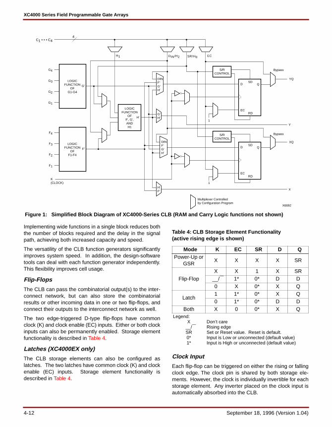
Configurable Logic Blocks (CLBs)Configurable Logic Blocks implement most of the logic inan FPGA. The principal CLB elements are shown inFigure 1. The number of CLBs needed to implementselected soft macros is shown in Table 3.
Two 4-input function generators (F and G) offer unrestrictedversatility. Most combinatorial logic functions need four orfewer inputs. However, a third function generator (H) is pro-vided. The H function generator has three inputs. Either
zero, one, or both of these inputs can be the outputs of Fand G; the other input(s) are from outside the CLB. TheCLB can, therefore, implement certain functions of up tonine variables, like parity check or expandable-identitycomparison of two sets of four inputs.
Each CLB contains two storage elements that can be usedto store the function generator outputs. However, the stor-age elements and function generators can also be usedindependently. These storage elements can be configuredas flip-flops in both XC4000E and XC4000EX devices; inthe XC4000EX they can optionally be configured aslatches. DIN can be used as a direct input to either of thetwo storage elements. H1 can drive the other through the Hfunction generator. Function generator outputs can alsodrive two outputs independent of the storage element out-puts. This versatility increases logic capacity and simplifiesrouting.
Thirteen CLB inputs and four CLB outputs provide accessto the function generators and storage elements. Theseinputs and outputs connect to the programmable intercon-nect resources outside the block.
Function Generators
Four independent inputs are provided to each of two func-tion generators (F1 - F4 and G1 - G4). These function gen-erators, with outputs labeled F’ and G’, are each capable ofimplementing any arbitrarily defined Boolean function offour inputs. The function generators are implemented asmemory look-up tables. The propagation delay is thereforeindependent of the function implemented.
A third function generator, labeled H’, can implement anyBoolean function of its three inputs. Two of these inputscan optionally be the F’ and G’ functional generator out-puts. Alternatively, one or both of these inputs can comefrom outside the CLB (H2, H0). The third input must comefrom outside the block (H1).
Signals from the function generators can exit the CLB ontwo outputs. F’ or H’ can be connected to the X output. G’or H’ can be connected to the Y output.
A CLB can be used to implement any of the following func-tions:
• any function of up to four variables, plus any second function of up to four unrelated variables, plus any third function of up to three unrelated variables1
• any single function of five variables • any function of four variables together with some
functions of six variables • some functions of up to nine variables.
1. When three separate functions are generated, one of the function outputs must be captured in a flip-flop internal to the CLB. Only two unregistered function generator outputs are available from the CLB.
September 18, 1996 (Version 1.04) 4-11
XC4000 Series Field Programmable Gate Arrays
Implementing wide functions in a single block reduces boththe number of blocks required and the delay in the signalpath, achieving both increased capacity and speed.
The versatility of the CLB function generators significantlyimproves system speed. In addition, the design-softwaretools can deal with each function generator independently.This flexibility improves cell usage.
Flip-Flops
The CLB can pass the combinatorial output(s) to the inter-connect network, but can also store the combinatorialresults or other incoming data in one or two flip-flops, andconnect their outputs to the interconnect network as well.
The two edge-triggered D-type flip-flops have commonclock (K) and clock enable (EC) inputs. Either or both clockinputs can also be permanently enabled. Storage elementfunctionality is described in Table 4.
Latches (XC4000EX only)
The CLB storage elements can also be configured aslatches. The two latches have common clock (K) and clockenable (EC) inputs. Storage element functionality isdescribed in Table 4.
Clock Input
Each flip-flop can be triggered on either the rising or fallingclock edge. The clock pin is shared by both storage ele-ments. However, the clock is individually invertible for eachstorage element. Any inverter placed on the clock input isautomatically absorbed into the CLB.
LOGIC FUNCTION
OF G1-G4
G4
G3
G2
G1
G'
LOGIC FUNCTION
OF F1-F4
F4
F3
F2
F1
F'
LOGIC FUNCTION
OF F', G', AND H1
H'
DIN F' G' H'
DIN F' G' H'
G' H'
H' F'
S/R CONTROL
D
ECRD
Bypass
Bypass
SDYQ
XQ
Q
S/R CONTROL
D
ECRD
SDQ
1
1
K (CLOCK)
Multiplexer Controlled by Configuration Program
Y
X
DIN/H2H1 SR/H0 EC
X6692
C1 • • • C4 4
Figure 1: Simplified Block Diagram of XC4000-Series CLB (RAM and Carry Logic functions not shown)
Table 4: CLB Storage Element Functionality (active rising edge is shown)
Mode K EC SR D QPower-Up or
GSRX X X X SR
Flip-FlopX X 1 X SR
__/ 1* 0* D D0 X 0* X Q
Latch1 1* 0* X Q0 1* 0* D D
Both X 0 0* X QLegend:
X__/ SR0*1*
Don’t careRising edgeSet or Reset value. Reset is default.Input is Low or unconnected (default value)Input is High or unconnected (default value)
4-12 September 18, 1996 (Version 1.04)

Clock Enable
The clock enable signal (EC) is active High. The EC pin isshared by both storage elements. If left unconnected foreither, the clock enable for that storage element defaults tothe active state. EC is not invertible within the CLB.
Set/Reset
An asynchronous storage element input (SR) can be con-figured as either set or reset. This configuration optiondetermines the state in which each flip-flop becomes oper-ational after configuration. It also determines the effect of aGlobal Set/Reset pulse during normal operation, and theeffect of a pulse on the SR pin of the CLB. All three set/reset functions for any single flip-flop are controlled by thesame configuration data bit.
The set/reset state can be independently specified for eachflip-flop. This input can also be independently disabled foreither flip-flop.
The set/reset state is specified by using the INIT attribute,or by placing the appropriate set or reset flip-flop librarysymbol.
SR is active High. It is not invertible within the CLB.
Global Set/Reset
A separate Global Set/Reset line (not shown in Figure 1)sets or clears each storage element during power-up,reconfiguration, or when a dedicated Reset net is drivenactive. This global net (GSR) does not compete with otherrouting resources; it uses a dedicated distribution network.
Each flip-flop is configured as either globally set or reset inthe same way that the local set/reset (SR) is specified.Therefore, if a flip-flop is set by SR, it is also set by GSR.Similarly, a reset flip-flop is reset by both SR and GSR.
GSR can be driven from any user-programmable pin as aglobal reset input. To use this global net, place an inputpad and input buffer in the schematic or HDL code, drivingthe GSR pin of the STARTUP symbol. (See Figure 2.) Aspecific pin location can be assigned to this input using aLOC attribute or property, just as with any other user-pro-grammable pad. An inverter can optionally be insertedafter the input buffer to invert the sense of the Global Set/Reset signal.
Alternatively, GSR can be driven from any internal node.
Data Inputs and Outputs
The source of a storage element data input is programma-ble. It is driven by any of the functions F’, G’, and H’, or bythe Direct In (DIN) block input. The flip-flops or latches drivethe XQ and YQ CLB outputs.
Two fast feed-through paths are available, as shown inFigure 1. A two-to-one multiplexer on each of the XQ andYQ outputs selects between a storage element output andany of the control inputs. This bypass is sometimes usedby the automated router to repower internal signals.
Control Signals
Multiplexers in the CLB map the four control inputs (C1 - C4in Figure 1) into the four internal control signals (H1, DIN/H2, SR/H0, and EC). Any of these inputs can drive any ofthe four internal control signals.
When the logic function is enabled, the four inputs are:
• EC — Enable Clock• SR/H0 — Asynchronous Set/Reset or H function
generator Input 0• DIN/H2 — Direct In or H function generator Input 2 • H1 — H function generator Input 1.
When the memory function is enabled, the four inputs are:
• EC — Enable Clock • WE — Write Enable • D0 — Data Input to F and/or G function generator • D1 — Data input to G function generator (16x1 and
16x2 modes) or 5th Address bit (32x1 mode).
Using FPGA Flip-Flops and Latches
The abundance of flip-flops in the XC4000 Series invitespipelined designs. This is a powerful way of increasing per-formance by breaking the function into smaller subfunc-tions and executing them in parallel, passing on the resultsthrough pipeline flip-flops. This method should be seriouslyconsidered wherever throughput is more important thanlatency.
To include a CLB flip-flop, place the appropriate librarysymbol. For example, FDCE is a D-type flip-flop with clockenable and asynchronous clear. The corresponding latchsymbol (for the XC4000EX only) is called LDCE.
In XC4000-Series devices, the flip flops can be used asregisters or shift registers without blocking the function gen-erators from performing a different, perhaps unrelated task.This ability increases the functional capacity of the devices.
The CLB setup time is specified between the function gen-erator inputs and the clock input K. Therefore, the specifiedCLB flip-flop setup time includes the delay through thefunction generator.
PAD
IBUF
GSRGTS
CLK DONEINQ1Q4
Q2Q3
STARTUP
X5260Figure 2: Schematic Symbols for Global Set/Reset
September 18, 1996 (Version 1.04) 4-13

XC4000 Series Field Programmable Gate Arrays
Using Function Generators as RAM
Optional modes for each CLB make the memory look-uptables in the F’ and G’ function generators usable as anarray of Read/Write memory cells. Available modes arelevel-sensitive (similar to the XC4000/A/H families), edge-triggered, and dual-port edge-triggered. Depending on theselected mode, a single CLB can be configured as either a16x2, 32x1, or 16x1 bit array.
Supported CLB memory configurations and timing modesfor single- and dual-port modes are shown in Table 5.
XC4000-Series devices are the first programmable logicdevices with edge-triggered (synchronous) and dual-portRAM accessible to the user. Edge-triggered RAM simpli-fies system timing. Dual-port RAM doubles the effectivethroughput of FIFO applications. These features can beindividually programmed in any XC4000-Series CLB.
Advantages of On-Chip and Edge-Triggered RAM
The on-chip RAM is extremely fast. The read access timeis the same as the logic delay. The write access time isslightly slower. Both access times are much faster thanany off-chip solution, because they avoid I/O delays.
Edge-triggered RAM, also called synchronous RAM, is afeature never before available in a Field ProgrammableGate Array. The simplicity of designing with edge-triggeredRAM, and the markedly higher achievable performance,add up to a significant improvement over existing deviceswith on-chip RAM.
Three application notes are available from Xilinx that dis-cuss edge-triggered RAM: “XC4000E Edge-Triggered andDual-Port RAM Capability,” “Implementing FIFOs inXC4000E RAM,” and “Synchronous and AsynchronousFIFO Designs.” All three application notes apply to bothXC4000E and XC4000EX RAM.
RAM Configuration Options
The function generators in any CLB can be configured asRAM arrays in the following sizes:
• Two 16x1 RAMs: two data inputs and two data outputs with identical or, if preferred, different addressing for each RAM
• One 32x1 RAM: one data input and one data output.
One F or G function generator can be configured as a 16x1RAM while the other function generators are used to imple-ment any function of up to 5 inputs.
Additionally, the XC4000-Series RAM may have either oftwo timing modes:
• Edge-Triggered (Synchronous): data written by the designated edge of the CLB clock. WE acts as a true clock enable.
• Level-Sensitive (Asynchronous): an external WE signal acts as the write strobe.
The selected timing mode applies to both function genera-tors within a CLB when both are configured as RAM.
The number of read ports is also programmable:
• Single Port: each function generator has a common read and write port
• Dual Port: both function generators are configured together as a single 16x1 dual-port RAM with one write port and two read ports. Simultaneous read and write operations to the same or different addresses are supported.
RAM configuration options are selected by placing theappropriate library symbol.
Choosing a RAM Configuration Mode
The appropriate choice of RAM mode for a given designshould be based on timing and resource requirements,desired functionality, and the simplicity of the design pro-cess. Recommended usage is shown in Table 6.
The difference between level-sensitive, edge-triggered,and dual-port RAM is only in the write operation. Readoperation and timing is identical for all modes of operation.
Table 5: Supported RAM Modes
16x 1
16x 2
32x 1
Edge-Triggered
Timing
Level-Sensitive Timing
Single-Port √ √ √ √ √Dual-Port √ √
Table 6: RAM Mode Selection
Level-Sensitive
Edge-Triggered
Dual-Port Edge-
TriggeredUse for New Designs?
No Yes Yes
Size (16x1,Registered)
1/2 CLB 1/2 CLB 1 CLB
Simultaneous Read/Write
No No Yes
Relative Performance
X 2X2X (4X
effective)
4-14 September 18, 1996 (Version 1.04)
G'4 G1 • • • G4
F1 • • • F4
C1 • • • C4
WRITE DECODER
1 of 16
DIN
16-LATCH ARRAY
X6752
4
4
MUX
F'WRITE
DECODER
1 of 16
DIN
16-LATCH ARRAY
READ ADDRESS
READ ADDRESS
WRITE PULSE
LATCH ENABLE
LATCH ENABLE
K (CLOCK)
WE D1 D0EC
WRITE PULSE
MUX4
4
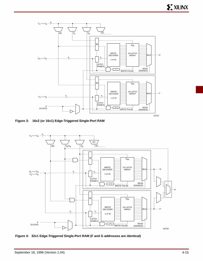
Figure 3: 16x2 (or 16x1) Edge-Triggered Single-Port RAM
G'4
G1 • • • G4 F1 • • • F4
C1 • • • C4
WRITE DECODER
1 of 16
DIN
16-LATCH ARRAY
X6754
4
4
MUX
F'WRITE
DECODER
1 of 16
DIN
16-LATCH ARRAY
READ ADDRESS
READ ADDRESS
WRITE PULSE
LATCH ENABLE
LATCH ENABLE
K (CLOCK)
WE D1/A4 D0
EC
EC
WRITE PULSE
MUX4
4
H'
Figure 4: 32x1 Edge-Triggered Single-Port RAM (F and G addresses are identical)
September 18, 1996 (Version 1.04) 4-15

XC4000 Series Field Programmable Gate Arrays
RAM Inputs and Outputs
The F1-F4 and G1-G4 inputs to the function generators actas address lines, selecting a particular memory cell in eachlook-up table.
The functionality of the CLB control signals changes whenthe function generators are configured as RAM. The DIN/H2, H1, and SR/H0 lines become the two data inputs (D0,D1) and the Write Enable (WE) input for the 16x2 memory.When the 32x1 configuration is selected, D1 acts as thefifth address bit and D0 is the data input.
The contents of the memory cell(s) being addressed areavailable at the F’ and G’ function-generator outputs. Theycan exit the CLB through its X and Y outputs, or can be cap-tured in the CLB flip-flop(s).
Configuring the CLB function generators as Read/Writememory does not affect the functionality of the other por-tions of the CLB, with the exception of the redefinition of thecontrol signals. In 16x2 and 16x1 modes, the H’ functiongenerator can be used to implement Boolean functions ofF’, G’, and D1, and the D flip-flops can latch the F’, G’, H’, orD0 signals.
Single-Port Edge-Triggered Mode
Edge-triggered (synchronous) RAM simplifies timingrequirements. XC4000-Series edge-triggered RAM timingoperates like writing to a data register. Data and addressare presented. The register is enabled for writing by a logicHigh on the write enable input, WE. Then a rising or fallingclock edge loads the data into the register, as shown inFigure 5.
Complex timing relationships between address, data, andwrite enable signals are not required, and the external writeenable pulse becomes a simple clock enable. The activeedge of WCLK latches the address, input data, and WE sig-nals. An internal write pulse is generated that performs thewrite. See Figure 3 and Figure 4 for block diagrams of aCLB configured as 16x2 and 32x1 edge-triggered, single-port RAM.
The relationships between CLB pins and RAM inputs andoutputs for single-port, edge-triggered mode are shown inTable 7.
The Write Clock input (WCLK) can be configured as activeon either the rising edge (default) or the falling edge. Ituses the same CLB pin (K) used to clock the CLB flip-flops,but it can be independently inverted. Consequently, theRAM output can optionally be registered within the same
CLB either by the same clock edge as the RAM, or by theopposite edge of this clock. The sense of WCLK applies toboth function generators in the CLB when both are config-ured as RAM.
The WE pin is active-High and is not invertible within theCLB.
Note: The pulse following the active edge of WCLK (TWPSin Figure 5) must be less than one millisecond wide. Formost applications, this requirement is not overly restrictive;however, it must not be forgotten. Stopping WCLK at thispoint in the write cycle could result in excessive current andeven damage to the larger devices if many CLBs are con-figured as edge-triggered RAM.
Table 7: Single-Port Edge-Triggered RAM Signals
RAM Signal CLB Pin FunctionD D0 or D1
(16x2, 16x1)D0 (32x1)
Data In
A[3:0] F1-F4 orG1-G4
Address
A[4] D1 (32x1) AddressWE WE Write EnableWCLK K ClockSPO (Data Out)
F’ or G’ Single Port Out(Data Out)
X6461
WCLK (K)
WE
ADDRESS
DATA IN
DATA OUT OLD NEW
TDSSTDHS
TASS TAHS
TWSS
TWPS
TWHS
TWOS
TILOTILO
Figure 5: Edge-Triggered RAM Write Timing
4-16 September 18, 1996 (Version 1.04)
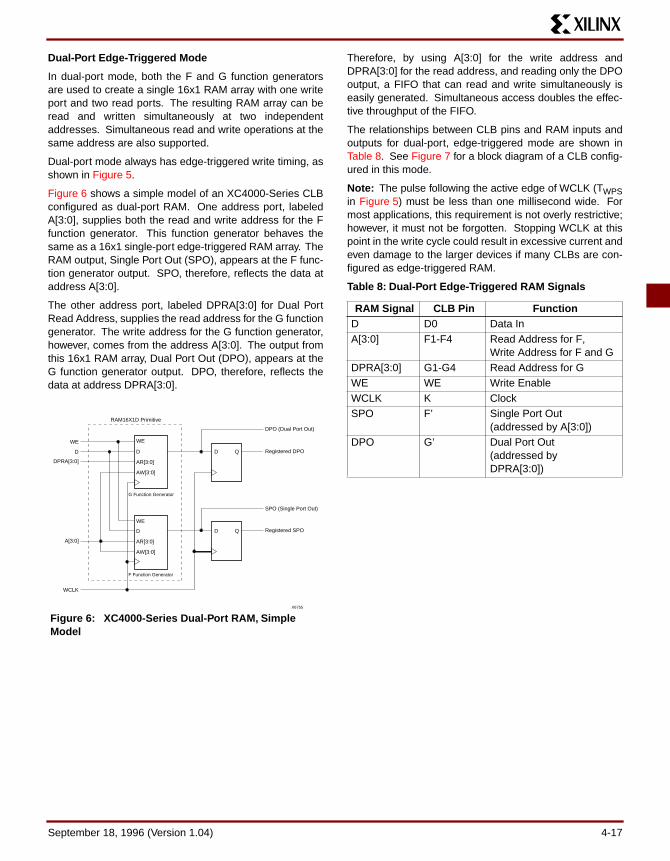
Dual-Port Edge-Triggered Mode
In dual-port mode, both the F and G function generatorsare used to create a single 16x1 RAM array with one writeport and two read ports. The resulting RAM array can beread and written simultaneously at two independentaddresses. Simultaneous read and write operations at thesame address are also supported.
Dual-port mode always has edge-triggered write timing, asshown in Figure 5.
Figure 6 shows a simple model of an XC4000-Series CLBconfigured as dual-port RAM. One address port, labeledA[3:0], supplies both the read and write address for the Ffunction generator. This function generator behaves thesame as a 16x1 single-port edge-triggered RAM array. TheRAM output, Single Port Out (SPO), appears at the F func-tion generator output. SPO, therefore, reflects the data ataddress A[3:0].
The other address port, labeled DPRA[3:0] for Dual PortRead Address, supplies the read address for the G functiongenerator. The write address for the G function generator,however, comes from the address A[3:0]. The output fromthis 16x1 RAM array, Dual Port Out (DPO), appears at theG function generator output. DPO, therefore, reflects thedata at address DPRA[3:0].
Therefore, by using A[3:0] for the write address andDPRA[3:0] for the read address, and reading only the DPOoutput, a FIFO that can read and write simultaneously iseasily generated. Simultaneous access doubles the effec-tive throughput of the FIFO.
The relationships between CLB pins and RAM inputs andoutputs for dual-port, edge-triggered mode are shown inTable 8. See Figure 7 for a block diagram of a CLB config-ured in this mode.
Note: The pulse following the active edge of WCLK (TWPSin Figure 5) must be less than one millisecond wide. Formost applications, this requirement is not overly restrictive;however, it must not be forgotten. Stopping WCLK at thispoint in the write cycle could result in excessive current andeven damage to the larger devices if many CLBs are con-figured as edge-triggered RAM.
Table 8: Dual-Port Edge-Triggered RAM Signals
WE WE
D D Q
D Q
D
DPRA[3:0]
A[3:0]
AR[3:0]
AW[3:0]
WE
D
AR[3:0]
AW[3:0]
RAM16X1D Primitive
F Function Generator
G Function Generator
DPO (Dual Port Out)
Registered DPO
SPO (Single Port Out)
Registered SPO
WCLK
X6755
Figure 6: XC4000-Series Dual-Port RAM, Simple Model
RAM Signal CLB Pin FunctionD D0 Data InA[3:0] F1-F4 Read Address for F,
Write Address for F and GDPRA[3:0] G1-G4 Read Address for GWE WE Write EnableWCLK K ClockSPO F’ Single Port Out
(addressed by A[3:0])DPO G’ Dual Port Out
(addressed byDPRA[3:0])
September 18, 1996 (Version 1.04) 4-17

XC4000 Series Field Programmable Gate Arrays
G'
G1 • • • G4
F1 • • • F4
WRITE DECODER
1 of 16
DIN
16-LATCH ARRAY
X6748
4
4
MUX
F'WRITE
DECODER
1 of 16
DIN
16-LATCH ARRAY
READ ADDRESS
READ ADDRESS
WRITE PULSE
LATCH ENABLE
LATCH ENABLE
K (CLOCK) WRITE PULSE
MUX4
4
C1 • • • C4 4
WE D1 D0 EC
Figure 7: 16x1 Edge-Triggered Dual-Port RAM
4-18 September 18, 1996 (Version 1.04)

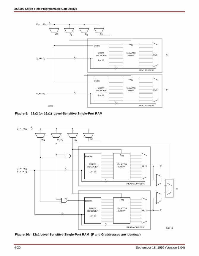
Single-Port Level-Sensitive Timing Mode
Note: Edge-triggered mode is recommended for all newdesigns. Level-sensitive mode, also called asynchronousmode, is still supported for XC4000-Series backward-com-patibility with the XC4000 family.
Level-sensitive RAM timing is simple in concept but can becomplicated in execution. Data and address signals arepresented, then a positive pulse on the write enable pin(WE) performs a write into the RAM at the designatedaddress. As indicated by the “level-sensitive” label, thisRAM acts like a latch. During the WE High pulse, changingthe data lines results in new data written to the old address.Changing the address lines while WE is High results in spu-rious data written to the new address—and possibly atother addresses as well, as the address lines inevitably donot all change simultaneously.
The user must generate a carefully timed WE signal. Thedelay on the WE signal and the address lines must be care-fully verified to ensure that WE does not become active untilafter the address lines have settled, and that WE goes inac-tive before the address lines change again. The data mustbe stable before and after the falling edge of WE.
In practical terms, WE is usually generated by a 2X clock. Ifa 2X clock is not available, the falling edge of the systemclock can be used. However, there are inherent risks in thisapproach, since the WE pulse must be guaranteed inactivebefore the next rising edge of the system clock. Severalolder application notes are available from Xilinx that dis-cuss the design of level-sensitive RAMs. These applicationnotes include XAPP031, “Using the XC4000 RAM Capabil-ity,” and XAPP042, “High-Speed RAM Design in XC4000.”
However, the edge-triggered RAM available in the XC4000Series is superior to level-sensitive RAM for almost everyapplication.
Figure 8 shows the write timing for level-sensitive, single-port RAM.
The relationships between CLB pins and RAM inputs andoutputs for single-port level-sensitive mode are shown inTable 9.
Figure 9 and Figure 10 show block diagrams of a CLB con-figured as 16x2 and 32x1 level-sensitive, single-port RAM.
Initializing RAM at Configuration
Both RAM and ROM implementations of the XC4000-Series devices are initialized during configuration. The ini-tial contents are defined via an INIT attribute or propertyattached to the RAM or ROM symbol, as described in theschematic library guide.
If not defined, all RAM contents are initialized to all zeros,by default.
RAM initialization occurs only during configuration. TheRAM content is not affected by Global Set/Reset.
Table 9: Single-Port Level-Sensitive RAM Signals
RAM Signal CLB Pin FunctionD D0 or D1 Data InA[3:0] F1-F4 or
G1-G4Address
WE WE Write EnableO F’ or G’ Data Out
WCT
ADDRESS
WRITE ENABLE
DATA IN
AST WPT
DST DHT
REQUIRED
AHT
X6462
Figure 8: Level-Sensitive RAM Write Timing
September 18, 1996 (Version 1.04) 4-19
XC4000 Series Field Programmable Gate Arrays
Enable
G'4 G1 • • • G4
F1 • • • F4
WRITE DECODER
1 of 16
DIN
16-LATCH ARRAY
X6746
4 READ ADDRESS
MUX
Enable
F'WRITE
DECODER
1 of 16
DIN
16-LATCH ARRAY
4 READ ADDRESS
MUX4
C1 • • • C4 4
WE D1 D0 EC
Figure 9: 16x2 (or 16x1) Level-Sensitive Single-Port RAM
Enable
WRITE DECODER
1 of 16
DIN
16-LATCH ARRAY
X6749
4
READ ADDRESS
MUX
Enable
WRITE DECODER
1 of 16
DIN
16-LATCH ARRAY
4
READ ADDRESS
MUX
G'4
G1 • • • G4 F1 • • • F4
C1 • • • C4 4
F'
WE D1/A4 D0 EC
4
H'
Figure 10: 32x1 Level-Sensitive Single-Port RAM (F and G addresses are identical)
4-20 September 18, 1996 (Version 1.04)
Fast Carry Logic
Each CLB F and G function generator contains dedicatedarithmetic logic for the fast generation of carry and borrowsignals. This extra output is passed on to the function gen-erator in the adjacent CLB. The carry chain is independentof normal routing resources.
Dedicated fast carry logic greatly increases the efficiencyand performance of adders, subtractors, accumulators,comparators and counters. It also opens the door to manynew applications involving arithmetic operation, where theprevious generations of FPGAs were not fast enough or tooinefficient. High-speed address offset calculations inmicroprocessor or graphics systems, and high-speed addi-tion in digital signal processing are two typical applications.
The two 4-input function generators can be configured as a2-bit adder with built-in hidden carry that can be expandedto any length. This dedicated carry circuitry is so fast andefficient that conventional speed-up methods like carrygenerate/propagate are meaningless even at the 16-bitlevel, and of marginal benefit at the 32-bit level.
This fast carry logic is one of the more significant featuresof the XC4000 Series, speeding up arithmetic and countinginto the 70 MHz range.
The carry chain in XC4000E devices can run either up ordown. At the top and bottom of the columns where thereare no CLBs above and below, the carry is propagated tothe right. (See Figure 11.) In order to improve speed in thehigh-capacity XC4000EX devices, which can potentiallyhave very long carry chains, the carry chain travels upwardonly, as shown in Figure 12. This restriction should have lit-tle impact, because the smallest XC4000EX device, theXC4028EX, can accommodate a 64-bit carry chain in a sin-gle column. Additionally, standard interconnect can beused to route a carry signal in the downward direction.
Figure 13 on page 22 shows an XC4000E CLB with dedi-cated fast carry logic. The carry logic in the XC4000EX issimilar, except that COUT exits at the top only, and the sig-nal CINDOWN does not exist. As shown in Figure 13, thecarry logic shares operand and control inputs with the func-tion generators. The carry outputs connect to the functiongenerators, where they are combined with the operands toform the sums.
Figure 14 and Figure 15 on page 23 show the details of thecarry logic for the XC4000E and the XC4000EX respec-tively. These diagrams show the contents of the boxlabeled “CARRY LOGIC” in Figure 13. As shown, theXC4000EX carry logic eliminated a multiplexer to reducedelay on the pass-through carry chain. Additionally, themultiplexer on the G4 path now has a memory-programma-ble input, which permits G4 to directly connect to COUT.G4 thus becomes an additional high-speed initializationpath for carry-in.
The dedicated carry logic is discussed in detail in Xilinxdocument XAPP 013: “Using the Dedicated Carry Logic inXC4000.” This discussion also applies to XC4000Edevices, and to XC4000EX devices when the minor logicchanges are taken into account.
The fast carry logic can be accessed by placing speciallibrary symbols, or by using Xilinx Relationally Placed Mac-ros (RPMs) that already include these symbols.
X6687
CLB CLB CLB CLB
CLB CLB CLB CLB
CLB
CLB
CLB
CLB
CLB
CLB
CLB
CLB
Figure 11: Available XC4000E Carry Propagation Paths
X6610
CLB CLB CLB CLB
CLB CLB CLB CLB
CLB
CLB
CLB
CLB
CLB
CLB
CLB
CLB
Figure 12: Available XC4000EX Carry Propagation Paths (dotted lines use general interconnect)
September 18, 1996 (Version 1.04) 4-21

XC4000 Series Field Programmable Gate Arrays
D QS/R
EC
YQ
Y
DIN
H
G
F
G
H
D QS/R
EC
XQ
DIN
H
G
F
H
X
H
F
G
G4
G3
G2
G1
FF3
F2
F1
F4
F CARRY
G CARRY
C C DOWNCARRY LOGIC
D
CC UP K S/R EC
H1
X6699
OUT
INOUT IN
IN
COUT0
Figure 13: Fast Carry Logic in XC4000E CLB (shaded area not present in XC4000EX)
4-22 September 18, 1996 (Version 1.04)

Figure 14: Detail of XC4000E Dedicated Carry Logic
0 1
0 1
M
M
0
1
0 1
M
0
1
M
1 0M
M 0
3
M
1
M
I
G1
G4
F2
F1
F3
COUT
G2
G3
F4
C INUP
C IN DOWN
X2000
TOFUNCTIONGENERATORS
M
M
M
COUT0
Figure 15: Detail of XC4000EX Dedicated Carry Logic (shaded areas show differences from XC4000E carry logic)
M
M
M
M
M
0 1
0 1
0
1
10
1
0
31
0M
M
M
M
M
F4
G3
G2
G1
G4
F2
F1
F3
M
TO FUNCTION GENERATORS
COUT
COUT0
CIN UPX6701
September 18, 1996 (Version 1.04) 4-23

XC4000 Series Field Programmable Gate Arrays
Input/Output Blocks (IOBs)User-configurable input/output blocks (IOBs) provide theinterface between external package pins and the internallogic. Each IOB controls one package pin and can be con-figured for input, output, or bidirectional signals.
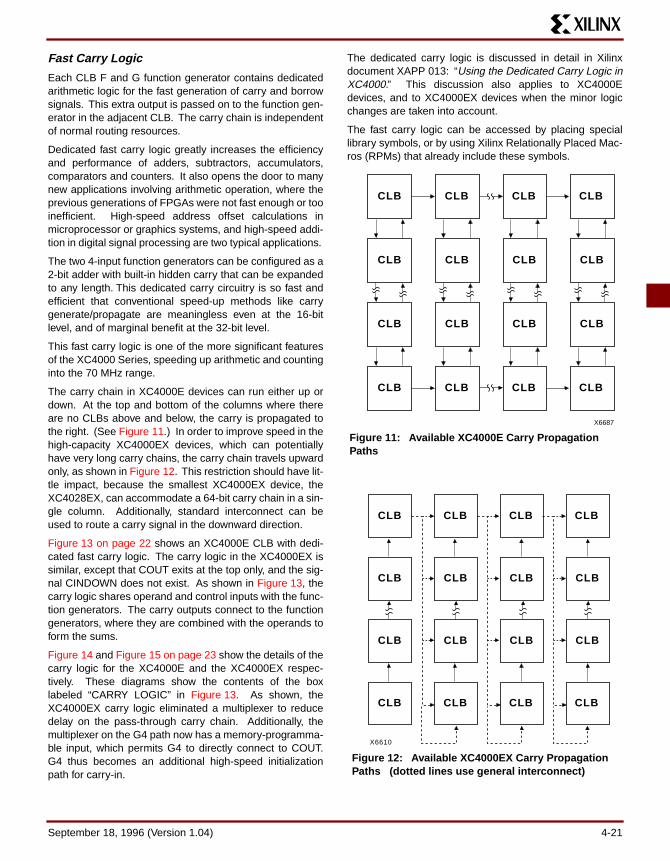
Figure 16 shows a simplified block diagram of theXC4000E IOB. A more complete diagram of the XC4000EIOB can be found in Figure 42 on page 51, in the “BoundaryScan” section. Figure 42 includes the boundary scan logicin the IOB.
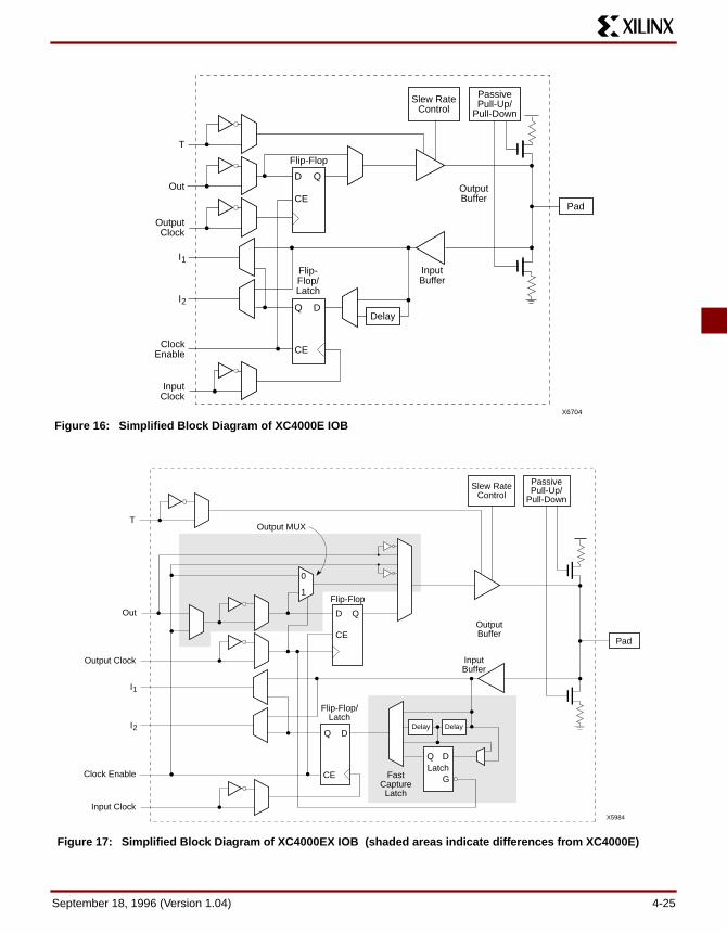
Figure 17 shows a simplified block diagram of theXC4000EX IOB. The XC4000EX IOB contains some spe-cial features not included in the XC4000E IOB. These fea-tures are highlighted in Figure 17, and discussedthroughout this section. When XC4000EX special featuresare discussed, they are clearly identified in the text. Anyfeature not so identified is present in both XC4000E andXC4000EX devices.
IOB Input Signals
Two paths, labeled I1 and I2 in Figure 16 and Figure 17,bring input signals into the array. Inputs also connect to aninput register that can be programmed as either an edge-triggered flip-flop or a level-sensitive latch.
The choice is made by placing the appropriate library sym-bol. For example, IFD is the basic input flip-flop (risingedge triggered), and ILD is the basic input latch (transpar-ent-High). Variations with inverted clocks are available, andsome combinations of latches and flip-flops can be imple-mented in a single IOB, as described in the XACT LibrariesGuide.
The inputs can be globally configured for either TTL (1.2V,default) or CMOS thresholds, using an option in the Make-Bits program. There is a slight hysteresis of about 300mV.The output levels are also configurable; the two globaladjustments of input threshold and output level are inde-pendent.
Inputs of the low-voltage devices must be configured asCMOS at all times. They can be driven by the outputs of all5-Volt XC4000-Series devices, provided that the 5-Volt out-puts are in TTL mode. They can also be driven by any TTLoutput that does not exceed 3.7 V. 5-Volt XC3000-familydevice outputs, for example, are TTL-compatible, but sincethe output voltage can exceed 3.7 V, they cannot be used todrive an XC4000L or XC4000XL input.
The inputs of XC4000-Series 5-Volt devices can be drivenby the outputs of any 3.3-Volt device, if the 5-Volt inputs arein TTL mode.
Supported sources for XC4000-Series device inputs areshown in Table 10.
Registered Inputs
The I1 and I2 signals that exit the block can each carryeither the direct or registered input signal.
The input and output storage elements in each IOB have acommon clock enable input, which, through configuration,can be activated individually for the input or output flip-flop,or both. This clock enable operates exactly like the EC pinon the XC4000-Series CLB. It cannot be inverted withinthe IOB.
The storage element behavior is shown in Table 11.
Table 11: Input Register Functionality (active rising edge is shown)
1. Acceptable for XC4000XL if the designated 5-Voltsupply pad (VTT) is tied to 5V.
Table 10: Supported Sources for XC4000-Series Device Inputs
Source
XC4000-Series Inputs3.3 V,
CMOS5 V,TTL
5 V, CMOS
Any device, Vcc = 3.3 V, CMOS outputs
√ √Unreli-
able Data
XC4000-Series, Vcc = 5 V,TTL outputs
√ √
Any device, Vcc = 5 V, TTL outputs (Voh ≤ 3.7 V)
√ √
Any device, Vcc = 5 V, CMOS outputs
Danger1 √ √
Mode ClockClock
EnableD Q
Power-Up or GSR
X X X SR
Flip-Flop __/ 1* D D0 X X Q
Latch 1 1* X Q 0 1* D D
Both X 0 X QLegend:
X__/ SR0*1*
Don’t careRising edgeSet or Reset value. Reset is default.Input is Low or unconnected (default value)Input is High or unconnected (default value)
4-24 September 18, 1996 (Version 1.04)
Q
Flip- Flop/ Latch
D
D
CE
CE
QOut
T
Output Clock
I
Input Clock
Clock Enable
Delay
Pad
Flip-Flop
Slew Rate Control
Output Buffer
Input Buffer
Passive Pull-Up/
Pull-Down
2
I1
X6704
Figure 16: Simplified Block Diagram of XC4000E IOB
Q
Flip-Flop/ Latch
Fast Capture Latch
D
Q Latch
D
G
D
0
1
CE
CE
QOut
T
Output Clock
I
Input Clock
Clock Enable
Pad
Flip-Flop
Slew Rate Control
Output Buffer
Output MUX
Input Buffer
Passive Pull-Up/
Pull-Down
2
I1
X5984
Delay Delay
Figure 17: Simplified Block Diagram of XC4000EX IOB (shaded areas indicate differences from XC4000E)
September 18, 1996 (Version 1.04) 4-25

XC4000 Series Field Programmable Gate Arrays
Optional Delay Guarantees Zero Hold Time
The data input to the register can optionally be delayed byseveral nanoseconds. With the delay enabled, the setuptime of the input flip-flop is increased so that normal clockrouting does not result in a positive hold-time requirement.A positive hold time requirement can lead to unreliable,temperature- or processing-dependent operation.
The input flip-flop setup time is defined between the datameasured at the device I/O pin and the clock input at theIOB (not at the clock pin). Any routing delay from thedevice clock pin to the clock input of the IOB must, there-fore, be subtracted from this setup time to arrive at the realsetup time requirement relative to the device pins. A shortspecified setup time might, therefore, result in a negativesetup time at the device pins, i.e., a positive hold-timerequirement.
When a delay is inserted on the data line, more clock delaycan be tolerated without causing a positive hold-timerequirement. Sufficient delay eliminates the possibility of adata hold-time requirement at the external pin. The maxi-mum delay is therefore inserted as the default.
The XC4000E IOB has a one-tap delay element: either thedelay is inserted (default), or it is not. The delay guaranteesa zero hold time with respect to clocks routed through anyof the XC4000E global clock buffers. (See “Global Netsand Buffers (XC4000E only)” on page 41 for a descriptionof the global clock buffers in the XC4000E.) For a shorterinput register setup time, with non-zero hold, attach aNODELAY attribute or property to the flip-flop.
The XC4000EX IOB has a two-tap delay element, withchoices of a full delay, a partial delay, or no delay. Theattributes or properties used to select the desired delay areshown in Table 12. The choices are no added attribute,MEDDELAY, and NODELAY. The default setting, with noadded attribute, ensures no hold time with respect to any ofthe XC4000EX clock buffers, including the Global Low-Skew buffers. MEDDELAY ensures no hold time withrespect to the Global Early and FastCLK buffers. Inputswith NODELAY may have a positive hold time with respectto all clock buffers, including the FastCLK buffers. For adescription of each of these buffers, see “Global Nets andBuffers (XC4000EX only)” on page 43.
Table 12: XC4000EX IOB Input Delay Element
Additional Input Latch for Fast Capture (XC4000EX only)
The XC4000EX IOB has an additional optional latch on theinput. This latch, as shown in Figure 17, is clocked by theoutput clock — the clock used for the output flip-flop —rather than the input clock. Therefore, two different clockscan be used to clock the two input storage elements. Thisadditional latch allows the very fast capture of input data,which is then synchronized to the internal clock by the IOBflip-flop or latch.
To use this Fast Capture technique, drive the output clockpin (the Fast Capture latching signal) from the output of oneof the Global Early or FastCLK buffers supplied in theXC4000EX. The second storage element should beclocked by a Global Low-Skew buffer, to synchronize theincoming data to the internal logic. (See Figure 18.) Thesespecial buffers are described in “Global Nets and Buffers(XC4000EX only)” on page 43.
The Fast Capture latch is designed primarily for use with aGlobal Early buffer. For Fast Capture, a single clock signalis routed through both a Global Early buffer and a GlobalLow-Skew buffer. (The two buffers share an input pad.)The Fast Capture latch is clocked by the Global Earlybuffer, and the standard IOB flip-flop or latch is clocked bythe Global Low-Skew buffer. This mode is the safest way touse the Fast Capture latch, because the clock buffers onboth storage elements are driven by the same pad. Thereis no external skew between clock pads to create potentialproblems.
Alternatively, a FastCLK buffer can be used to minimize thesetup time of device inputs, if a positive hold time is accept-able. Use the FastCLK buffer to clock the Fast Capturelatch, and a slower clock buffer to clock the standard IOBflip-flop or latch. Either the Global Early buffer or the GlobalLow-Skew buffer can be used for the second storage ele-
Value When to Usefull delay (default, no attribute added)
Zero Hold with respect to Global Low-Skew Buffer, Global Early Buffer, or FastCLK Buffer
MEDDELAY Zero Hold with respect to Global Early Buffer or FastCLK Buffer
NODELAY Short Setup, positive Hold time
IPAD
IPAD
IPAD
IPAD
IPAD
BUFGE
BUFFCLK
BUFGLS
BUFGLSNODELAY
C
C
CE
CE
D Q
GF
D Q
GF
to internal logic
to internal logic
ILFFX
ILFFX
X6705
Figure 18: Examples Using XC4000EX Fast Capture Latch
4-26 September 18, 1996 (Version 1.04)
ment, but whichever one is used should be the same clockas the related internal logic. Since the FastCLK pads aredifferent from the Global Early and Global Low-Skew pads,care must be taken to ensure that skew external to thedevice does not create internal timing difficulties.
To place the Fast Capture latch in a design, use one of thespecial library symbols, ILFFX or ILFLX. ILFFX is a trans-parent-Low Fast Capture latch followed by an active-Highinput flip-flop. ILFLX is a transparent-Low Fast Capturelatch followed by a transparent-High input latch. Any of theclock inputs can be inverted before driving the library ele-ment, and the inverter is absorbed into the IOB. If a singleBUFG output is used to drive both clock inputs, the soft-ware automatically runs the clock through both a GlobalLow-Skew buffer and a Global Early buffer, and clocks theFast Capture latch appropriately.
Figure 17 on page 25 also shows a two-tap delay on theinput. By default, if the Fast Capture latch is used, the Xilinxsoftware assumes a Global Early buffer is driving the clock,and selects MEDDELAY to ensure a zero hold time. Thisdefault can be overridden to remove the delay, if FastClk isused, by attaching a NODELAY attribute or property to theILFFX or ILFLX latch. Select the desired delay based onthe discussion in the previous subsection.
IOB Output Signals
Output signals can be optionally inverted within the IOB,and can pass directly to the pad or be stored in an edge-triggered flip-flop. The functionality of this flip-flop is shownin Table 13.
An active-High 3-state signal can be used to place the out-put buffer in a high-impedance state, implementing 3-stateoutputs or bidirectional I/O. Under configuration control,the output (OUT) and output 3-state (T) signals can beinverted. The polarity of these signals is independentlyconfigured for each IOB.
The 4-mA maximum output current specification of manyFPGAs often forces the user to add external buffers, whichare especially cumbersome on bidirectional I/O lines. TheXC4000E and XC4000EX devices solve many of theseproblems by providing a guaranteed output sink current of12 mA. Two adjacent outputs can be interconnected exter-nally to sink up to 24 mA. (XC4000L and XC4000XL out-puts can sink up to 4 mA, and two adjacent XC4000L andXC4000XL outputs can sink up to 8 mA.) The XC4000Eand XC4000EX FPGAs can thus directly drive buses on aprinted circuit board.
By default, the output pull-up structure is configured as aTTL-like totem-pole. The High driver is an n-channel pull-up transistor, pulling to a voltage one transistor thresholdbelow Vcc. Alternatively, the outputs can be globally con-figured as CMOS drivers, with p-channel pull-up transistorspulling to Vcc. This MakeBits option applies to all outputson the device. It is not individually programmable.
Outputs of low-voltage devices must be configured asCMOS at all times. They can drive the inputs of any 5-Voltdevice with TTL-compatible thresholds.
Any XC4000-Series 5-Volt device with its outputs config-ured in TTL mode can drive the inputs of any typical 3.3-Volt device. (For a detailed discussion of how to interfacebetween 5 V and 3.3 V devices, see the 3V Products sec-tion of The Programmable Logic Data Book.)
Supported destinations for XC4000-Series device outputsare shown in Table 14.
Table 14: Supported Destinations for XC4000-Series Outputs
1. Only if destination device has 5-V tolerant inputs
Table 13: Output Flip-Flop Functionality (active rising edge is shown)
Mode ClockClock
Enable T D QPower-Upor GSR
X X 0* X SR
Flip-Flop
X 0 0* X Q__/ 1* 0* D DX X 1 X Z0 X 0* X Q
Legend:X
__/ SR0*1*Z
Don’t careRising edgeSet or Reset value. Reset is default.Input is Low or unconnected (default value)Input is High or unconnected (default value)3-state
Destination
XC4000-Series Outputs
3.3 V,CMOS
5 V,TTL
5 V, CMOS
Any typical device, Vcc = 3.3 V, CMOS-threshold inputs
√ √ some1
Any device, Vcc = 5 V, TTL-threshold inputs
√ √ √
Any device, Vcc = 5 V, CMOS-threshold inputs
Unreliable Data
√
September 18, 1996 (Version 1.04) 4-27

XC4000 Series Field Programmable Gate Arrays
An output can be configured as open-drain (open-collector)by placing an OBUFT symbol in a schematic or HDL code,then tying the 3-state pin (T) to the output signal, and theinput pin (I) to Ground. (See Figure 19.)
Output Slew Rate
The slew rate of each output buffer is, by default, reduced,to minimize power bus transients when switching non-criti-cal signals. For critical signals, attach a FAST attribute orproperty to the output buffer or flip-flop.
For XC4000E devices, maximum total capacitive load forsimultaneous fast mode switching in the same direction is200 pF for all package pins between each Power/Groundpin pair. For XC4000EX devices, additional internal Power/Ground pin pairs are connected to special Power andGround planes within the packages, to reduce groundbounce. Therefore, the maximum total capacitive load is300 pF between each external Power/Ground pin pair.Maximum loading may vary for the low-voltage devices.
For slew-rate limited outputs this total is two times larger foreach device type: 400 pF for XC4000E devices and 600 pFfor XC4000EX devices. This maximum capacitive loadshould not be exceeded, as it can result in ground bounceof greater than 1.5 V amplitude and more than 5 ns dura-tion. This level of ground bounce may cause undesiredtransient behavior on an output, or in the internal logic.This restriction is common to all high-speed digital ICs, andis not particular to Xilinx or the XC4000 Series.
XC4000-Series devices have a feature called “Soft Start-up,” designed to reduce ground bounce when all outputsare turned on simultaneously at the end of configuration.When the configuration process is finished and the devicestarts up, the first activation of the outputs is automaticallyslew-rate limited. Immediately following the initial activationof the I/O, the slew rate of the individual outputs is deter-mined by the individual configuration option for each IOB.
Global Three-State
A separate Global 3-State line (not shown in Figure 16 orFigure 17) forces all FPGA outputs to the high-impedancestate, unless boundary scan is enabled and is executing anEXTEST instruction. This global net (GTS) does not com-pete with other routing resources; it uses a dedicated distri-bution network.
GTS can be driven from any user-programmable pin as aglobal 3-state input. To use this global net, place an inputpad and input buffer in the schematic or HDL code, drivingthe GTS pin of the STARTUP symbol. A specific pin loca-tion can be assigned to this input using a LOC attribute orproperty, just as with any other user-programmable pad.An inverter can optionally be inserted after the input bufferto invert the sense of the Global 3-State signal. Using GTSis similar to GSR. See Figure 2 on page 13 for details.
Alternatively, GTS can be driven from any internal node.
Output Multiplexer/2-Input Function Generator (XC4000EX only)
As shown in Figure 17 on page 25, the output path in theXC4000EX IOB contains an additional multiplexer not avail-able in the XC4000E IOB. The multiplexer can also be con-figured as a 2-input function generator, implementing apass-gate, AND-gate, OR-gate, or XOR-gate, with 0, 1, or 2inverted inputs. The logic used to implement these func-tions is shown in the upper gray area of Figure 17.
When configured as a multiplexer, this feature allows twooutput signals to time-share the same output pad; effec-tively doubling the number of device outputs without requir-ing a larger, more expensive package.
When the MUX is configured as a 2-input function genera-tor, logic can be implemented within the IOB itself. Com-bined with either a FastCLK or Global Early buffer, thisarrangement allows very high-speed gating of a single sig-nal. For example, a wide decoder can be implemented inCLBs, and its output gated with a Read or Write Strobedriven by a FastCLK buffer, as shown in Figure 20. Thecritical-path pin-to-pin delay of this circuit is less than 6nanoseconds. (This value may not be achievable inXC4000XL devices.)
As shown in Figure 17, the IOB input pins Out, OutputClock, and Clock Enable have different delays and differentflexibilities regarding polarity. Additionally, Output Clocksources are more limited than the other inputs. Therefore,the Xilinx software does not move logic into the IOB func-tion generators unless explicitly directed to do so.
X6702
OPADOBUFT
Figure 19: Open-Drain Output
IPAD
F OPADFAST
BUFFCLK
OAND2from internal logic
X6698
Figure 20: Fast Pin-to-Pin Path in XC4000E
4-28 September 18, 1996 (Version 1.04)

The user can specify that the IOB function generator beused, by placing special library symbols beginning with theletter “O.” For example, a 2-input AND-gate in the IOB func-tion generator is called OAND2. Use the symbol input pinlabelled “F” for the signal on the critical path. This signal isplaced on the OK pin — the IOB input with the shortestdelay to the function generator. Two examples are shown inFigure 21.
Other IOB Options
There are a number of other programmable options in theXC4000-Series IOB.
Pull-up and Pull-down Resistors
Programmable pull-up and pull-down resistors are usefulfor tying unused pins to Vcc or Ground to minimize powerconsumption and reduce noise sensitivity. The configurablepull-up resistor is a p-channel transistor that pulls to Vcc.The configurable pull-down resistor is an n-channel transis-tor that pulls to Ground.
The value of these resistors is 50 kΩ − 100 kΩ. This highvalue makes them unsuitable as wired-AND pull-up resis-tors.
The pull-up resistors for most user-programmable IOBs areactive during the configuration process. See Table 24 onpage 78 for a list of pins with pull-ups active before and dur-ing configuration.
After configuration, voltage levels of unused pads, bondedor unbonded, must be valid logic levels, to reduce noisesensitivity and avoid excess current. Therefore, by default,unused pads are configured with the internal pull-up resis-tor active. Alternatively, they can be individually configuredwith the pull-down resistor, or as a driven output, or to bedriven by an external source. To activate the internal pull-up, attach the PULLUP library component to the netattached to the pad. To activate the internal pull-down,attach the PULLDOWN library component to the netattached to the pad.
Independent Clocks
Separate clock signals are provided for the input and outputflip-flops. The clock can be independently inverted for eachflip-flop within the IOB, generating either falling-edge or ris-ing-edge triggered flip-flops. The clock inputs for each IOB
are independent, except that in the XC4000EX, the FastCapture latch shares an IOB input with the output clock pin.
Early Clock for IOBs (XC4000EX only)
Special early clocks are available for IOBs. These clocksare sourced by the same sources as the Global Low-Skewbuffers, but are separately buffered. They have fewer loadsand therefore less delay. The early clock can drive eitherthe IOB output clock or the IOB input clock, or both. Theearly clock allows fast capture of input data, and fast clock-to-output on output data. The Global Early buffers thatdrive these clocks are described in “Global Nets and Buff-ers (XC4000EX only)” on page 43.
Fast Clock for IOBs (XC4000EX only)
Very fast clocks driven by FastCLK buffers are also avail-able for IOBs. These clocks are sourced by semi-dedicatedpads—the pads can be used as general I/O if not used todrive FastCLK buffers. There are two FastCLK buffers onthe left edge, and two on the right edge of the device. Theyprovide the fastest method of reaching the IOB clock pins.The FastCLK buffer can drive either the IOB output clock orthe IOB input clock, or both. These buffers allow the fastestpossible setup times and clock-to-output times. The Fast-CLK buffers are described in “Global Nets and Buffers(XC4000EX only)” on page 43.
Global Set/Reset
As with the CLB registers, the Global Set/Reset signal(GSR) can be used to set or clear the input and output reg-isters, depending on the value of the INIT attribute or prop-erty. The two flip-flops can be individually configured to setor clear on reset and after configuration. Other than theglobal GSR net, no user-controlled set/reset signal is avail-able to the I/O flip-flops. The choice of set or clear appliesto both the initial state of the flip-flop and the response tothe Global Set/Reset pulse. See “Global Set/Reset” onpage 13 for a description of how to use GSR.
JTAG Support
Embedded logic attached to the IOBs contains test struc-tures compatible with IEEE Standard 1149.1 for boundaryscan testing, permitting easy chip and board-level testing.More information is provided in “Boundary Scan” onpage 50.
Three-State Buffers A pair of 3-state buffers is associated with each CLB in thearray. (See Figure 27 on page 34.) These 3-state bufferscan be used to drive signals onto the nearest horizontallonglines above and below the CLB. They can therefore beused to implement multiplexed or bidirectional buses on thehorizontal longlines, saving logic resources. Programma-ble pull-up resistors attached to these longlines help toimplement a wide wired-AND function.
OAND2
F
X6598
D0
S0
D1O
OMUX2
X6599
Figure 21: Output AND and MUX Symbols in XC4000EX IOB
September 18, 1996 (Version 1.04) 4-29

XC4000 Series Field Programmable Gate Arrays
The buffer enable is an active-High 3-state (i.e. an active-Low enable), as shown in Table 15.
Another 3-state buffer with similar access is located neareach I/O block along the right and left edges of the array.(See Figure 33 on page 39.)
The horizontal longlines driven by the 3-state buffers have aweak keeper at each end. This circuit prevents undefinedfloating levels. However, it is overridden by any driver, evena pull-up resistor.
Special longlines running along the perimeter of the arraycan be used to wire-AND signals coming from nearby IOBsor from internal longlines. These longlines form the wideedge decoders discussed in “Wide Edge Decoders” onpage 31.
Three-State Buffer Modes
The 3-state buffers can be configured in three modes:
• Standard 3-state buffer• Wired-AND with input on the I pin• Wired OR-AND
Standard 3-State Buffer
All three pins are used. Place the library element BUFT.Connect the input to the I pin and the output to the O pin.The T pin is an active-High 3-state (i.e. an active-Lowenable). Tie the T pin to Ground to implement a standardbuffer.
Wired-AND with Input on the I Pin
The buffer can be used as a Wired-AND. Use the WAND1library symbol, which is essentially an open-drain buffer.
WAND4, WAND8, and WAND16 are also available. Seethe XACT Libraries Guide for further information.
The T pin is internally tied to the I pin. Connect the input tothe I pin and the output to the O pin. Connect the outputs ofall the WAND1s together and attach a PULLUP symbol.
Wired OR-AND
The buffer can be configured as a Wired OR-AND. A Highlevel on either input turns off the output. Use theWOR2AND library symbol, which is essentially an open-drain 2-input OR gate. The two input pins are functionallyequivalent. Attach the two inputs to the I0 and I1 pins andtie the output to the O pin. Tie the outputs of all theWOR2ANDs together and attach a PULLUP symbol.
Three-State Buffer Examples
Figure 22 shows how to use the 3-state buffers to imple-ment a wired-AND function. When all the buffer inputs areHigh, the pull-up resistor(s) provide the High output.
Figure 23 shows how to use the 3-state buffers to imple-ment a multiplexer. The selection is accomplished by thebuffer 3-state signal.
Pay particular attention to the polarity of the T pin whenusing these buffers in a design. Active-High 3-state (T) isidentical to an active-Low output enable, as shown inTable 15.
Table 15: Three-State Buffer Functionality
IN T OUTX 1 ZIN 0 IN
P U L L
U P
Z = DA
DB
(DC
+DD
) (DE
+DF)
DE
DF
DC
DD
DB
DA
WAND1 WAND1W0R2AND W0R2AND
X6465
Figure 22: Open-Drain Buffers Implement a Wired-AND Function
DNDCDBDA
A B C N
Z = DA • A + DB • B + DC • C + DN • N~100 kΩ
"Weak Keeper"
X6466
BUFT BUFT BUFT BUFT
Figure 23: 3-State Buffers Implement a Multiplexer
4-30 September 18, 1996 (Version 1.04)

Wide Edge Decoders Dedicated decoder circuitry boosts the performance ofwide decoding functions. When the address or data field iswider than the function generator inputs, FPGAs needmulti-level decoding and are thus slower than PALs.XC4000-Series CLBs have nine inputs. Any decoder of upto nine inputs is, therefore, compact and fast. However,there is also a need for much wider decoders, especially foraddress decoding in large microprocessor systems.
An XC4000-Series FPGA has four programmable decod-ers located on each edge of the device. The inputs to eachdecoder are any of the IOB I1 signals on that edge plus onelocal interconnect per CLB row or column. Each row or col-umn of CLBs provides up to three variables or their compli-ments., as shown in Figure 24. Each decoder generates aHigh output (resistor pull-up) when the AND condition ofthe selected inputs, or their complements, is true. This isanalogous to a product term in typical PAL devices.
Each of these wired-AND gates is capable of accepting upto 42 inputs on the XC4005E and 72 on the XC4013E.There are up to 96 inputs for each decoder on theXC4028EX and 132 on the XC4052EX. The decoders mayalso be split in two when a larger number of narrowerdecoders are required, for a maximum of 32 decoders perdevice.
The decoder outputs can drive CLB inputs, so they can becombined with other logic to form a PAL-like AND/OR struc-ture. The decoder outputs can also be routed directly to thechip outputs. For fastest speed, the output should be onthe same chip edge as the decoder. Very large PALs canbe emulated by ORing the decoder outputs in a CLB. Thisdecoding feature covers what has long been considered aweakness of older FPGAs. Users often resorted to exter-nal PALs for simple but fast decoding functions. Now, thededicated decoders in the XC4000-Series device canimplement these functions fast and efficiently.
To use the wide edge decoders, place one or more of theWAND library symbols (WAND1, WAND4, WAND8,WAND16). Attach a DECODE attribute or property to eachWAND symbol. Tie the outputs together and attach a PUL-LUP symbol. Location attributes or properties such as L(left edge) or TR (right half of top edge) should also be usedto ensure the correct placement of the decoder inputs.
On-Chip Oscillator XC4000-Series devices include an internal oscillator. Thisoscillator is used to clock the power-on time-out, for config-uration memory clearing, and as the source of CCLK inMaster configuration modes. The oscillator runs at a nom-inal 8 MHz frequency that varies with process, Vcc, andtemperature. The output frequency falls between 4 and 10MHz. (The oscillator operates more slowly at lower volt-ages. The output frequency may be reduced by as muchas 10% for low-voltage devices.)
The oscillator output is optionally available after configura-tion. Any two of four resynchronized taps of a built-individer are also available. These taps are at the fourth,ninth, fourteenth and nineteenth bits of the divider. There-fore, if the primary oscillator output is running at the nomi-nal 8 MHz, the user has access to an 8 MHz clock, plus anytwo of 500 kHz, 16kHz, 490Hz and 15Hz (up to 10% lowerfor low-voltage devices). These frequencies can vary by asmuch as -50% or +25%.
These signals can be accessed by placing the OSC4library element in a schematic or in HDL code (seeFigure 25).
The oscillator is automatically disabled after configuration ifthe OSC4 symbol is not used in the design.
IOBIOB
BA
INTERCONNECT
( C) .....
(A • B • C) .....
(A • B • C) .....
(A • B • C) .....
.I1.I1
X2627
C
Figure 24: XC4000-Series Edge Decoding Example
F16K
F500K
F8M
F490
F15
X6703
OSC4
Figure 25: XC4000-Series Oscillator Symbol
September 18, 1996 (Version 1.04) 4-31

XC4000 Series Field Programmable Gate Arrays
Programmable Interconnect All internal connections are composed of metal segmentswith programmable switching points and switching matricesto implement the desired routing. A structured, hierarchicalmatrix of routing resources is provided to achieve efficientautomated routing.
The XC4000E and XC4000EX share a basic interconnectstructure. XC4000EX devices, however, have additionalrouting not available in the XC4000E. The extra routingresources allow high utilization in high-capacity devices.All XC4000EX-specific routing resources are clearly identi-fied throughout this section. Any resources not identifiedas XC4000EX-specific are present in all XC4000-Seriesdevices.
This section describes the varied routing resources avail-able in XC4000-Series devices. The implementation soft-ware automatically assigns the appropriate resourcesbased on the density and timing requirements of thedesign.
Interconnect OverviewThere are several types of interconnect.
• CLB routing is associated with each row and column of the CLB array.
• IOB routing forms a ring (called a VersaRing) around the outside of the CLB array. It connects the I/O with the internal logic blocks.
• Global routing consists of dedicated networks primarily designed to distribute clocks throughout the device with minimum delay and skew. Global routing can also be used for other high-fanout signals.
Five interconnect types are distinguished by the relativelength of their segments: single-length lines, double-lengthlines, quad and octal lines (XC4000EX only), and longlines.In the XC4000EX, direct connects allow fast data flowbetween adjacent CLBs, and between IOBs and CLBs.
Extra routing is included in the IOB pad ring. TheXC4000EX also includes a ring of octal interconnect linesnear the IOBs to improve pin-swapping and routing tolocked pins.
XC4000E devices include two types of global buffers, whileXC4000EX devices have three different types. These glo-bal buffers have different properties, and are intended fordifferent purposes. They are discussed in detail later in thissection.
CLB Routing Connections A high-level diagram of the routing resources associatedwith one CLB is shown in Figure 26. The shaded arrowsrepresent routing present only in XC4000EX devices.
Table 16 shows how much routing of each type is availablein XC4000E and XC4000EX CLB arrays. Clearly, verylarge designs, or designs with a great deal of interconnect,will route more easily in the XC4000EX. Smaller XC4000Edesigns, typically requiring significantly less interconnect,do not require the additional routing.
Figure 27 on page 34 is a detailed diagram of both theXC4000E and the XC4000EX CLB, with associated rout-ing. The shaded square is the programmable switchmatrix, present in both the XC4000E and the XC4000EX.The L-shaped shaded area is present only in XC4000EXdevices. As shown in the figure, the XC4000EX block isessentially an XC4000E block with additional routing.
CLB inputs and outputs are distributed on all four sides,providing maximum routing flexibility. In general, the entirearchitecture is symmetrical and regular. It is well suited toestablished placement and routing algorithms. Inputs, out-puts, and function generators can freely swap positionswithin a CLB to avoid routing congestion during the place-ment and routing operation.
Table 16: Routing per CLB in XC4000-Series Devices
XC4000E XC4000EXVertical Horizontal Vertical Horizontal
Singles 8 8 8 8Doubles 4 4 4 4Quads 0 0 12 12Longlines 6 6 10 6Direct Connects
0 0 2 2
Globals 4 0 8 0Carry Logic 2 0 1 0Total 24 18 45 32
4-32 September 18, 1996 (Version 1.04)
x5994
Quad
Quad
Single
Double
Long
Direct Connect
Long
CLB
Long Global Clock
Long Double Single Global Clock
Carry Chain
Direct Connect
Figure 26: High-Level Routing Diagram of XC4000-Series CLB (shaded arrows indicate XC4000EX only)
September 18, 1996 (Version 1.04) 4-33

XC4000 Series Field Programmable Gate Arrays
F1
C1
G1
F2 C2 G2
F3
C3
G3
F4 C4 G4
K
X
Y
XQ
YQ
LONGSING
LE
DOUBLE
LONG
GLO
BAL
QUAD
LONG
SINGLE
DOUBLE
LONG
LONG
DOUBLE
DOUBLE
QUAD
GLO
BAL
Common to XC4000E and XC4000EX
XC4000EX only
Programmable Switch Matrix
CLB
DIRECTFEEDBACK
DIRECT
FEEDBACK
Figure 27: Detail of Programmable Interconnect Associated with XC4000-Series CLB
4-34 September 18, 1996 (Version 1.04)

Programmable Switch Matrices
The horizontal and vertical single- and double-length linesintersect at a box called a programmable switch matrix(PSM). Each switch matrix consists of programmable passtransistors used to establish connections between the lines(see Figure 28).
For example, a single-length signal entering on the rightside of the switch matrix can be routed to a single-lengthline on the top, left, or bottom sides, or any combinationthereof, if multiple branches are required. Similarly, a dou-ble-length signal can be routed to a double-length line onany or all of the other three edges of the programmableswitch matrix.
Single-Length Lines
Single-length lines provide the greatest interconnect flexi-bility and offer fast routing between adjacent blocks. Thereare eight vertical and eight horizontal single-length linesassociated with each CLB. These lines connect the switch-ing matrices that are located in every row and a column ofCLBs.
Single-length lines are connected by way of the program-mable switch matrices, as shown in Figure 29. Routingconnectivity is shown in Figure 27.
Single-length lines incur a delay whenever they go througha switching matrix. Therefore, they are not suitable for rout-ing signals for long distances. They are normally used toconduct signals within a localized area and to provide thebranching for nets with fanout greater than one.
Double-Length Lines
The double-length lines consist of a grid of metal segments,each twice as long as the single-length lines: they run pasttwo CLBs before entering a switch matrix. Double-lengthlines are grouped in pairs with the switch matrices stag-gered, so that each line goes through a switch matrix atevery other row or column of CLBs (see Figure 29).
There are four vertical and four horizontal double-lengthlines associated with each CLB. These lines provide fastersignal routing over intermediate distances, while retainingrouting flexibility. Double-length lines are connected by wayof the programmable switch matrices. Routing connectivityis shown in Figure 27.
Six Pass Transistors Per Switch Matrix Interconnect Point
Singles
Double
Double
Single
s
Double
Double
X6600
Figure 28: Programmable Switch Matrix (PSM)
CLB
PSM PSM
PSMPSM
CLB CLB
CLB CLB CLB
CLB CLB CLB
Doubles
Singles
Doubles
X6601
Figure 29: Single- and Double-Length Lines, with Programmable Switch Matrices (PSMs)
September 18, 1996 (Version 1.04) 4-35

XC4000 Series Field Programmable Gate Arrays
Quad Lines (XC4000EX only)
XC4000EX devices also include twelve vertical and twelvehorizontal quad lines per CLB row and column. Quad linesare four times as long as the single-length lines. They areinterconnected via buffered switch matrices (shown as dia-monds in Figure 27 on page 34). Quad lines run past fourCLBs before entering a buffered switch matrix. They aregrouped in fours, with the buffered switch matrices stag-gered, so that each line goes through a buffered switchmatrix at every fourth CLB location in that row or column.(See Figure 30.)
The buffered switch matrixes have four pins, one on eachedge. All of the pins are bidirectional. Any pin can driveany or all of the other pins.
Each buffered switch matrix contains one buffer and sixpass transistors. It resembles the programmable switchmatrix shown in Figure 28, with the addition of a program-mable buffer. There can be up to two independent inputsand up to two independent outputs. Only one of the inde-pendent inputs can be buffered.
The place and route software automatically uses the timingrequirements of the design to determine whether or not aquad line signal should be buffered. A heavily loaded sig-nal is typically buffered, while a lightly loaded one is not.One scenario is to alternate buffers and pass transistors.This allows both vertical and horizontal quad lines to bebuffered at alternating buffered switch matrices.
Due to the buffered switch matrices, quad lines are veryfast. They provide the fastest available method of routingheavily loaded signals for long distances across the device.
CLB
CLB
CLB
CLB
CLB
CLB
CLB
CLB
CLB
CLB
CLB
CLB
CLB
CLB
CLB
CLB
CLB
CLB
CLB
CLB
CLB
CLB
CLB
CLB
CLB
X6602Figure 30: Quad Lines (XC4000EX only)
4-36 September 18, 1996 (Version 1.04)

Longlines
Longlines form a grid of metal interconnect segments thatrun the entire length or width of the array. Longlines areintended for high fan-out, time-critical signal nets, or netsthat are distributed over long distances. In XC4000EXdevices, quad lines are preferred for critical nets, becausethe buffered switch matrices make them faster for high fan-out nets.
Two horizontal longlines per CLB can be driven by 3-stateor open-drain drivers (TBUFs). They can therefore imple-ment unidirectional or bidirectional buses, wide multiplex-ers, or wired-AND functions. (See “Three-State Buffers” onpage 29 for more details.)
Each horizontal longline driven by TBUFs has either two(XC4000E) or eight (XC4000EX) pull-up resistors. To acti-vate these resistors, attach a PULLUP symbol to the long-line net. The software automatically activates the appropri-ate number of pull-ups. There is also a weak keeper ateach end of these two horizontal longlines. This circuit pre-vents undefined floating levels. However, it is overridden byany driver, even a pull-up resistor.
Each XC4000E longline has a programmable splitter switchat its center, as does each XC4000EX longline driven byTBUFs. This switch can separate the line into two indepen-dent routing channels, each running half the width or heightof the array.
Each XC4000EX longline not driven by TBUFs has a buff-ered programmable splitter switch at the 1/4, 1/2, and 3/4points of the array. Due to the buffering, XC4000EX lon-gline performance does not deteriorate with the larger arraysizes. If the longline is split, the resulting partial longlinesare independent.
Routing connectivity of the longlines is shown in Figure 27on page 34.
Direct Interconnect (XC4000EX only)
The XC4000EX offers two direct, efficient and fast connec-tions between adjacent CLBs. These nets facilitate a dataflow from the left to the right side of the device, or from thetop to the bottom, as shown in Figure 31. Signals routed onthe direct interconnect exhibit minimum interconnect prop-agation delay and use no general routing resources.
The direct interconnect is also present between CLBs andadjacent IOBs. Each IOB on the left and top device edgeshas a direct path to the nearest CLB. Each CLB on theright and bottom edges of the array has a direct path to thenearest two IOBs, since there are two IOBs for each row orcolumn of CLBs.
The place and route software uses direct interconnectwhenever possible, to maximize routing resources and min-imize interconnect delays.
CLBIOB
X6603
IOB
IOB
IOB
IOB
IOB
IOB
IOB
IOB
IOB
IOB
IOB
IOB
IOB
IOB
IOB
IOB
IOB
IOB
IOBCLB
CLB
CLB
CLB
CLB
~~~~
~~~~
~~~~ ~~~~ ~~~~
Figure 31: XC4000EX Direct Interconnect
September 18, 1996 (Version 1.04) 4-37

XC4000 Series Field Programmable Gate Arrays
I/O RoutingXC4000-Series devices have additional routing around theIOB ring. This routing is called a VersaRing. TheVersaRing facilitates pin-swapping and redesign withoutaffecting board layout. Included are eight double-lengthlines spanning two CLBs (four IOBs), and four longlines.Global lines and Wide Edge Decoder lines are provided.XC4000EX devices also include eight octal lines.
A high-level diagram of the VersaRing is shown inFigure 32. The shaded arrows represent routing presentonly in XC4000EX devices.
Figure 33 is a detailed diagram of the XC4000E andXC4000EX VersaRing. The area shown includes two IOBs.There are two IOBs per CLB row or column, therefore thisdiagram corresponds to the CLB routing diagram shown inFigure 27 on page 34. The shaded areas represent routingand routing connections present only in XC4000EXdevices.
X5995
Direct Connect
Edge Decode
Double Long Global Clock
Octal
Quad
Single
Double
Long
Direct Connect
Long
INTERCONNECT
IOBWED
WED
WEDIOB
Figure 32: High-Level Routing Diagram of XC4000-Series VersaRing (Left Edge) WED = Wide Edge Decoder, IOB = I/O Block (shaded arrows indicate XC4000EX only)
4-38 September 18, 1996 (Version 1.04)

TO
CLB
ARRAY
IK
OK
I1
CE
I2
DE
CO
DE
R
T O
OCTAL
EDGEDECODE
QUAD
LONG
SINGLE
DOUBLE
LONG
LONG
DOUBLE
DOUBLE
GLOBAL
IK
OK
I1
CE
I2
T O
DE
CO
DE
RD
EC
OD
ER
Common to XC4000E and XC4000EX
XC4000EX only
IOB
IOB
DIRECT
Figure 33: Detail of Programmable Interconnect Associated with XC4000-Series IOB (Left Edge)
September 18, 1996 (Version 1.04) 4-39

XC4000 Series Field Programmable Gate Arrays
Octal I/O Routing (XC4000EX only)
Between the XC4000EX CLB array and the pad ring, eightinterconnect tracks provide for versatility in pin assignmentand fixed pinout flexibility. (See Figure 34.)
These routing tracks are called octals, because they can bebroken every eight CLBs (sixteen IOBs) by a programma-ble buffer that also functions as a splitter switch. The buff-ers are staggered, so each line goes through a buffer atevery eighth CLB location around the device edge.
The octal lines bend around the corners of the device. Thelines cross at the corners in such a way that the segment
most recently buffered before the turn has the farthest dis-tance to travel before the next buffer, as shown inFigure 34.
IOB inputs and outputs interface with the octal lines via thesingle-length interconnect lines. Single-length lines arealso used for communication between the octals and dou-ble-length lines, quads, and longlines within the CLB array.
Segmentation into buffered octals was found to be optimalfor distributing signals over long distances around thedevice.
Segment with nearest buffer connects to segment with furthest buffer
IOB
IOB
IOB
IOBIOB
IOB
IOB
IOB
X6607
Figure 34: XC4000EX Octal I/O Routing
4-40 September 18, 1996 (Version 1.04)
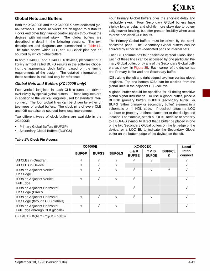
Global Nets and BuffersBoth the XC4000E and the XC4000EX have dedicated glo-bal networks. These networks are designed to distributeclocks and other high fanout control signals throughout thedevices with minimal skew. The global buffers aredescribed in detail in the following sections. The textdescriptions and diagrams are summarized in Table 17.The table shows which CLB and IOB clock pins can besourced by which global buffers.
In both XC4000E and XC4000EX devices, placement of alibrary symbol called BUFG results in the software choos-ing the appropriate clock buffer, based on the timingrequirements of the design. The detailed information inthese sections is included only for reference.
Global Nets and Buffers (XC4000E only)
Four vertical longlines in each CLB column are drivenexclusively by special global buffers. These longlines arein addition to the vertical longlines used for standard inter-connect. The four global lines can be driven by either oftwo types of global buffers. The clock pins of every CLBand IOB can also be sourced from local interconnect.
Two different types of clock buffers are available in theXC4000E:
• Primary Global Buffers (BUFGP)• Secondary Global Buffers (BUFGS)
Four Primary Global buffers offer the shortest delay andnegligible skew. Four Secondary Global buffers haveslightly longer delay and slightly more skew due to poten-tially heavier loading, but offer greater flexibility when usedto drive non-clock CLB inputs.
The Primary Global buffers must be driven by the semi-dedicated pads. The Secondary Global buffers can besourced by either semi-dedicated pads or internal nets.
Each CLB column has four dedicated vertical Global lines.Each of these lines can be accessed by one particular Pri-mary Global buffer, or by any of the Secondary Global buff-ers, as shown in Figure 35. Each corner of the device hasone Primary buffer and one Secondary buffer.
IOBs along the left and right edges have four vertical globallonglines. Top and bottom IOBs can be clocked from theglobal lines in the adjacent CLB column.
A global buffer should be specified for all timing-sensitiveglobal signal distribution. To use a global buffer, place aBUFGP (primary buffer), BUFGS (secondary buffer), orBUFG (either primary or secondary buffer) element in aschematic or in HDL code. If desired, attach a LOCattribute or property to direct placement to the designatedlocation. For example, attach a LOC=L attribute or propertyto a BUFGS symbol to direct that a buffer be placed in oneof the two Secondary Global buffers on the left edge of thedevice, or a LOC=BL to indicate the Secondary Globalbuffer on the bottom edge of the device, on the left.
L = Left, R = Right, T = Top, B = Bottom
Table 17: Clock Pin Access
XC4000E XC4000EX LocalInter-
connectBUFGP BUFGS BUFGLSL & R
BUFGET & B
BUFGEBUFFCL
KAll CLBs in Quadrant √ √ √ √ √ √All CLBs in Device √ √ √ √IOBs on Adjacent Vertical Half Edge
√ √ √ √ √ √ √
IOBs on Adjacent Vertical Full Edge
√ √ √ √ √
IOBs on Adjacent Horizontal Half Edge (Direct)
√ √
IOBs on Adjacent Horizontal Half Edge (through CLB globals)
√ √ √ √ √ √
IOBs on Adjacent Horizontal Full Edge (through CLB globals)
√ √ √ √
September 18, 1996 (Version 1.04) 4-41

XC4000 Series Field Programmable Gate Arrays
X4 X4
X6604
X4
4
One BUFGP per Global Line
One BUFGP per Global Line
Any BUFGS Any BUFGS
BUFGP
PGCK4SGCK4
PGCK3SGCK3
BUFGS
BUFGP
BUFGS
IOB
IOB
IOBIOBIOBIOB
IOBIOBIOB
IOB
IOB
BUFGS
BUFGS
BUFGP
BUFGP
SGCK1
PGCK1
SGCK2PGCK2
IOB
X4locals
localslocals
locals
loca
ls
loca
ls
loca
ls
loca
ls
loca
ls
loca
ls
loca
ls
loca
ls
4
4 4
CLB
CLB
locals locals
CLB
CLBlocals locals
Figure 35: XC4000E Global Net Distribution
X4
4
IOB CLOCKS
CLB CLOCKS (PER COLUMN)
CLB CLOCKS (PER COLUMN)
CLB CLOCKS (PER COLUMN)
CLB CLOCKS (PER COLUMN)
locals
locals
locals
locals
localsBUFGLS
localsBUFGLS
BUFGLS
BUFGLS BUFGLS
BUFGE
BUFGE
BUFGE
BUFGE
BUFGE
BUFGE
BUFGE BUFGE
BUFGLS BUFGLSIOB IOB IOB IOB
IOB IOB IOB IOB
BUFGLS BUFGLS
BUFGLS BUFGLS
GCK8 GCK7GCK1 GCK6
BUFFCLK BUFFCLK
BUFFCLK
FCLK1 FCLK4
FCLK2
BUFFCLK
FCLK3
GCK2 GCK5GCK3 GCK4
IOB
IOB
IOB
IOB
locals
BUFGLSlocals
BUFGLSlocals
localsBUFGLS
localsBUFGLS
IOB CLOCKS
IOB CLOCKS
IOB CLOCKS
4
X8
X8X4
X6694
8
8
8 8
8 BUFGLSlocals
88 8
8 8
8
8
8
8
CLB
CLB
CLB
CLB
loca
ls
loca
ls
loca
ls
loca
ls
loca
ls
loca
ls
loca
ls
loca
ls
X8
X8
X8
X8
Figure 36: XC4000EX Global Net Distribution
4-42 September 18, 1996 (Version 1.04)

Global Nets and Buffers (XC4000EX only)
Eight vertical longlines in each CLB column are driven byspecial global buffers. These longlines are in addition tothe vertical longlines used for standard interconnect. Theglobal lines are broken in the center of the array, to allowfaster distribution and to minimize skew across the wholearray. Each half-column global line has its own bufferedmultiplexer, as shown in Figure 36. The top and bottom glo-bal lines cannot be connected across the center of thedevice, as this connection might introduce unacceptableskew. The top and bottom halves of the global lines mustbe separately driven — although they can be driven by thesame global buffer.
The eight global lines in each CLB column can be driven byeither of two types of global buffers. They can also bedriven by internal logic, because they can be accessed bysingle, double, and quad lines at the top, bottom, half, andquarter points. Consequently, the number of differentclocks that can be used simultaneously in an XC4000EXdevice is very large.
There are four global lines feeding the IOBs at the left edgeof the device. IOBs along the right edge have eight globallines. There is a single global line along the top and bottomedges with access to the IOBs. All IOB global lines are bro-ken at the center. They cannot be connected across thecenter of the device, as this connection might introduceunacceptable skew.
IOB global lines can be driven from any of three types ofglobal buffers, or from local interconnect. Alternatively, topand bottom IOBs can be clocked from the global lines in theadjacent CLB column.
Three different types of clock buffers are available in theXC4000EX:
• Global Low-Skew Buffers (BUFGLS)• Global Early Buffers (BUFGE)• FastCLK Buffers (BUFFCLK)
Global Low-Skew Buffers are the standard clock buffers.They should be used for most internal clocking, whenever alarge portion of the device must be driven.
Global Early Buffers are designed to provide a faster clockaccess, but CLB access is limited to one-fourth of thedevice. They also facilitate a faster I/O interface.
FastCLK buffers are specifically designed to provide thefastest possible I/O clock. They have only the standardinput access to CLBs, through local interconnect.
Figure 36 is a conceptual diagram of the global net struc-ture in the XC4000EX.
Global Early buffers and Global Low-Skew buffers share asingle pad. Therefore, the same IPAD symbol can driveone buffer of each type, in parallel. This configuration isparticularly useful when using the Fast Capture latches, asdescribed in “IOB Input Signals” on page 24. Paired Global
Early and Global Low-Skew buffers share a common input;they cannot be driven by two different signals.
Choosing an XC4000EX Clock Buffer
The clocking structure of the XC4000EX provides a largevariety of features. However, it can be simple to use, with-out understanding all the details. The software automati-cally handles clocks, along with all other routing, when theappropriate clock buffer is placed in the design. In fact, if abuffer symbol called BUFG is placed, rather than a specifictype of buffer, the software even chooses the buffer mostappropriate for the design. The detailed information in thissection is provided for those users who want a finer level ofcontrol over their designs.
If fine control is desired, use the following summary andTable 17 on page 41 to choose an appropriate clock buffer.
• The simplest thing to do is to use a Global Low-Skew buffer.
• If a faster clock path is needed, try a BUFG. The software will first try to use a Global Low-Skew Buffer. If timing requirements are not met, a faster buffer will automatically be used.
• If a single quadrant of the chip is sufficient for the clocked logic, and the timing requires a faster clock than the Global Low-Skew buffer, use a Global Early buffer.
• In special cases, where both external and internal timing have been carefully studied, a FastCLK buffer can be used, for the fastest possible I/O clock path.
Global Low-Skew Buffers
Each corner of the XC4000EX device has two Global Low-Skew buffers. Any of the eight Global Low-Skew bufferscan drive any of the eight vertical Global lines in a columnof CLBs. In addition, any of the buffers can drive any of thefour vertical lines accessing the IOBs on the left edge of thedevice, and any of the eight vertical lines accessing theIOBs on the right edge of the device. (See Figure 37 onpage 44.)
IOBs at the top and bottom edges of the device areaccessed through the vertical Global lines in the CLB array,as in the XC4000E. Any Global Low-Skew buffer can,therefore, access every IOB and CLB in the device.
The Global Low-Skew buffers can be driven by either semi-dedicated pads or internal logic.
To use a Global Low-Skew buffer, place a BUFGLS ele-ment in a schematic or in HDL code. If desired, attach aLOC attribute or property to direct placement to the desig-nated location. For example, attach a LOC=T attribute orproperty to direct that a BUFGLS be placed in one of thetwo Global Low-Skew buffers on the top edge of the device,or a LOC=TR to indicate the Global Low-Skew buffer on thetop edge of the device, on the right.
September 18, 1996 (Version 1.04) 4-43

XC4000 Series Field Programmable Gate Arrays
Global Early Buffers
Each corner of the XC4000EX device has two Global Earlybuffers. The primary purpose of the Global Early buffers isto provide an earlier clock access than the potentiallyheavily-loaded Global Low-Skew buffers. A clock sourceapplied to both buffers will result in the Global Early clockedge occurring several nanoseconds earlier than the Glo-bal Low-Skew buffer clock edge, due to the lighter loading.
Global Early buffers also facilitate the fast capture of deviceinputs, using the Fast Capture latches described in “IOBInput Signals” on page 24. For Fast Capture, take a singleclock signal, and route it through both a Global Early bufferand a Global Low-Skew buffer. (The two buffers share aninput pad.) Use the Global Early buffer to clock the FastCapture latch, and the Global Low-Skew buffer to clock thenormal input flip-flop or latch, as shown in Figure 18 onpage 26.
The Global Early buffers can also be used to provide a fastClock-to-Out on device output pins. However, an earlyclock in the output flip-flop IOB must be taken into consid-eration when calculating the internal clock speed for thedesign.
The Global Early buffers at the left and right edges of thechip have slightly different capabilities than the ones at thetop and bottom. Refer to Figure 38, Figure 39, andFigure 36 on page 42 while reading the following explana-tion.
Each Global Early buffer can access the eight vertical Glo-bal lines for all CLBs in the quadrant. Therefore, only one-fourth of the CLB clock pins can be accessed. This restric-tion is in large part responsible for the faster speed of thebuffers, relative to the Global Low-Skew buffers.
The left-side Global Early buffers can each drive two of thefour vertical lines accessing the IOBs on the entire left edgeof the device. The right-side Global Early buffers can eachdrive two of the eight vertical lines accessing the IOBs onthe entire right edge of the device. (See Figure 38.)
Each left and right Global Early buffer can also drive half ofthe IOBs along either the top or bottom edge of the device,using a dedicated line that can only be accessed throughthe Global Early buffers.
The top and bottom Global Early buffers can drive half ofthe IOBs along either the left or right edge of the device, asshown in Figure 39. They can only access the top and bot-tom IOBs via the CLB global lines.
1 6
2 5
3
8
4
7
CLB CLB
CLBCLB
I O B
I O B
I O B
I O B
IOB IOB
IOBIOB
X6753
Figure 37: Any BUFGLS (GCK1 - GCK8) Can Drive Any or All Clock Inputs on the Device
1 6
2 5
3
8
4
7
CLB CLB
CLBCLB
I O B
I O B
I O B
I O B
IOB IOB
IOBIOB
X6751
Figure 38: Left and Right BUFGEs Can Drive Any or All Clock Inputs in Same Quadrant or Edge (GCK1 is shown. GCK2, GCK5 and GCK6 are similar.)
1 6
2 5
3
8
4
7
CLB CLB
CLBCLB
I O B
I O B
I O B
I O B
IOB IOB
IOBIOB
X6747
Figure 39: Top and Bottom BUFGEs Can Drive Any or All Clock Inputs in Same Quadrant (GCK8 is shown. GCK3, GCK4 and GCK7 are similar.)
4-44 September 18, 1996 (Version 1.04)
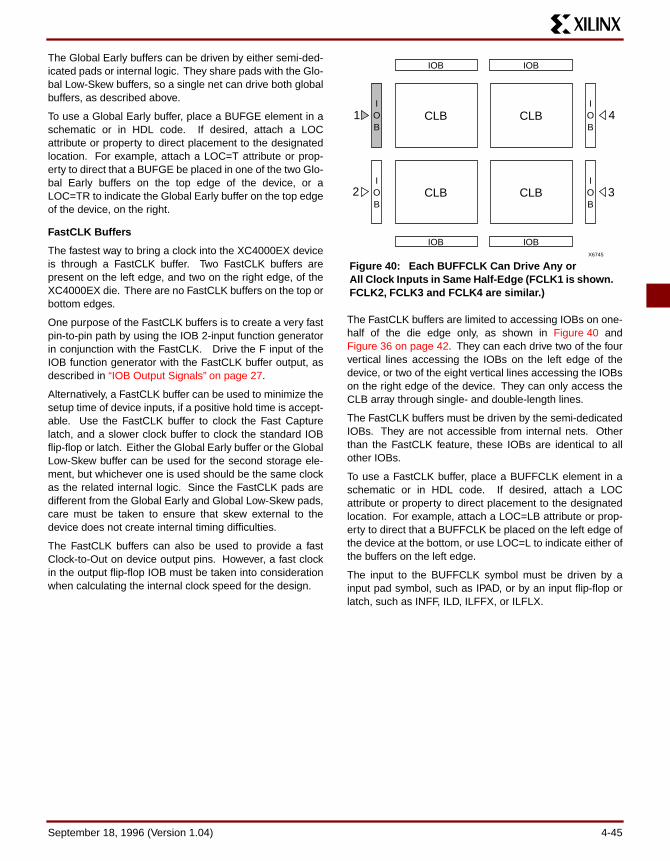
The Global Early buffers can be driven by either semi-ded-icated pads or internal logic. They share pads with the Glo-bal Low-Skew buffers, so a single net can drive both globalbuffers, as described above.
To use a Global Early buffer, place a BUFGE element in aschematic or in HDL code. If desired, attach a LOCattribute or property to direct placement to the designatedlocation. For example, attach a LOC=T attribute or prop-erty to direct that a BUFGE be placed in one of the two Glo-bal Early buffers on the top edge of the device, or aLOC=TR to indicate the Global Early buffer on the top edgeof the device, on the right.
FastCLK Buffers
The fastest way to bring a clock into the XC4000EX deviceis through a FastCLK buffer. Two FastCLK buffers arepresent on the left edge, and two on the right edge, of theXC4000EX die. There are no FastCLK buffers on the top orbottom edges.
One purpose of the FastCLK buffers is to create a very fastpin-to-pin path by using the IOB 2-input function generatorin conjunction with the FastCLK. Drive the F input of theIOB function generator with the FastCLK buffer output, asdescribed in “IOB Output Signals” on page 27.
Alternatively, a FastCLK buffer can be used to minimize thesetup time of device inputs, if a positive hold time is accept-able. Use the FastCLK buffer to clock the Fast Capturelatch, and a slower clock buffer to clock the standard IOBflip-flop or latch. Either the Global Early buffer or the GlobalLow-Skew buffer can be used for the second storage ele-ment, but whichever one is used should be the same clockas the related internal logic. Since the FastCLK pads aredifferent from the Global Early and Global Low-Skew pads,care must be taken to ensure that skew external to thedevice does not create internal timing difficulties.
The FastCLK buffers can also be used to provide a fastClock-to-Out on device output pins. However, a fast clockin the output flip-flop IOB must be taken into considerationwhen calculating the internal clock speed for the design.
The FastCLK buffers are limited to accessing IOBs on one-half of the die edge only, as shown in Figure 40 andFigure 36 on page 42. They can each drive two of the fourvertical lines accessing the IOBs on the left edge of thedevice, or two of the eight vertical lines accessing the IOBson the right edge of the device. They can only access theCLB array through single- and double-length lines.
The FastCLK buffers must be driven by the semi-dedicatedIOBs. They are not accessible from internal nets. Otherthan the FastCLK feature, these IOBs are identical to allother IOBs.
To use a FastCLK buffer, place a BUFFCLK element in aschematic or in HDL code. If desired, attach a LOCattribute or property to direct placement to the designatedlocation. For example, attach a LOC=LB attribute or prop-erty to direct that a BUFFCLK be placed on the left edge ofthe device at the bottom, or use LOC=L to indicate either ofthe buffers on the left edge.
The input to the BUFFCLK symbol must be driven by ainput pad symbol, such as IPAD, or by an input flip-flop orlatch, such as INFF, ILD, ILFFX, or ILFLX.
1 4
2 3
CLB CLB
CLBCLB
I O B
I O B
I O B
I O B
IOB IOB
IOBIOBX6745
Figure 40: Each BUFFCLK Can Drive Any or All Clock Inputs in Same Half-Edge (FCLK1 is shown. FCLK2, FCLK3 and FCLK4 are similar.)
September 18, 1996 (Version 1.04) 4-45

XC4000 Series Field Programmable Gate Arrays
Power Distribution Power for the FPGA is distributed through a grid to achievehigh noise immunity and isolation between logic and I/O.Inside the FPGA, a dedicated Vcc and Ground ring sur-rounding the logic array provides power to the I/O drivers,as shown in Figure 41. An independent matrix of Vcc andGround lines supplies the interior logic of the device.
This power distribution grid provides a stable supply andground for all internal logic, providing the external packagepower pins are all connected and appropriately decoupled.Typically, a 0.1 µF capacitor connected near the Vcc andGround pins of the package will provide adequate decou-pling.
Output buffers capable of driving/sinking the specified 12mA (XC4000E) or 24 mA (XC4000EX) loads under speci-fied worst-case conditions may be capable of driving/sink-ing up to 10 times as much current under best caseconditions.
Noise can be reduced by minimizing external load capaci-tance and reducing simultaneous output transitions in thesame direction. It may also be beneficial to locate heavilyloaded output buffers near the Ground pads. The I/O Blockoutput buffers have a slew-rate limited mode (default) whichshould be used where output rise and fall times are notspeed-critical.
Pin Descriptions There are three types of pins in the XC4000-Seriesdevices:
• Permanently dedicated pins• User I/O pins that can have special functions • Unrestricted user-programmable I/O pins.
Before and during configuration, all outputs not used for theconfiguration process are 3-stated with a 50 kΩ - 100 kΩpull-up resistor.
After configuration, if an IOB is unused it is configured asan input with a 50 kΩ - 100 kΩ pull-up resistor.
XC4000-Series devices have no dedicated Reset input.Any user I/O can be configured to drive the Global Set/Reset net, GSR. See “Global Set/Reset” on page 13 formore information on GSR.
XC4000-Series devices have no Powerdown control input,as the XC3000 and XC2000 families do. The XC3000/XC2000 Powerdown control also 3-stated all of the device I/O pins. For XC4000-Series devices, use the global 3-statenet, GTS, instead. This net 3-states all outputs, but doesnot place the device in low-power mode. See “IOB OutputSignals” on page 27 for more information on GTS.
Device pins for XC4000-Series devices are described inTable 18. Pin functions during configuration for each of theseven configuration modes are summarized in Table 24 onpage 78, in the “Configuration Timing” section.GND
Ground and Vcc Ring for I/O Drivers
Vcc
GND
Vcc
Logic Power Grid
X5422
Figure 41: XC4000-Series Power Distribution
4-46 September 18, 1996 (Version 1.04)

Table 18: Pin Descriptions
Pin Name
I/O During Config.
I/O After
Config. Pin DescriptionPermanently Dedicated Pins
VCC I IEight or more (depending on package) connections to the nominal +5 V supply voltage (+3.3 V for low-voltage devices). All must be connected, and each must be decoupled with a 0.01 - 0.1 µF capacitor to Ground.
GND I IEight or more (depending on package type) connections to Ground. All must be con-nected.
CCLK I or O I
During configuration, Configuration Clock (CCLK) is an output in Master modes or Asyn-chronous Peripheral mode, but is an input in Slave mode, Synchronous Peripheral mode, and Express mode. After configuration, CCLK has a weak pull-up resistor and can be selected as the Readback Clock. There is no CCLK High time restriction on XC4000-Series devices, except during Readback. See “Violating the Maximum High and Low Time Specification for the Readback Clock” on page 65 for an explanation of this exception.
DONE I/O O
DONE is a bidirectional signal with an optional internal pull-up resistor. As an output, it indicates the completion of the configuration process. As an input, a Low level on DONE can be configured to delay the global logic initialization and the enabling of out-puts.The optional pull-up resistor is selected as an option in MakeBits, the XACTstep pro-gram that creates the configuration bitstream. The resistor is included by default.
PROGRAM I I
PROGRAM is an active Low input that forces the FPGA to clear its configuration mem-ory. It is used to initiate a configuration cycle. When PROGRAM goes High, the FPGA finishes the current clear cycle and executes another complete clear cycle, before it goes into a WAIT state and releases INIT. The PROGRAM pin has a permanent weak pull-up, so it need not be externally pulled up to Vcc.
User I/O Pins That Can Have Special Functions
RDY/BUSY O I/O
During Peripheral mode configuration, this pin indicates when it is appropriate to write another byte of data into the FPGA. The same status is also available on D7 in Asyn-chronous Peripheral mode, if a read operation is performed when the device is selected. After configuration, RDY/BUSY is a user-programmable I/O pin. RDY/BUSY is pulled High with a high-impedance pull-up prior to INIT going High.
RCLK O I/O
During Master Parallel configuration, each change on the A0-A17 outputs (A0 - A21 for XC4000EX) is preceded by a rising edge on RCLK, a redundant output signal. RCLK is useful for clocked PROMs. It is rarely used during configuration. After configuration, RCLK is a user-programmable I/O pin.
M0, M1, M2 II (M0),O (M1),I (M2)
As Mode inputs, these pins are sampled after INIT goes High to determine the configu-ration mode to be used. After configuration, M0 and M2 can be used as inputs, and M1 can be used as a 3-state output. These three pins have no associated input or output registers. During configuration, these pins have weak pull-up resistors. For the most popular con-figuration mode, Slave Serial, the mode pins can thus be left unconnected. The three mode inputs can be individually configured with or without weak pull-up or pull-down re-sistors. A pull-down resistor value of 4.7 kΩ is recommended.These pins can only be used as inputs or outputs when called out by special schematic definitions. To use these pins, place the library components MD0, MD1, and MD2 in-stead of the usual pad symbols. Input or output buffers must still be used.
September 18, 1996 (Version 1.04) 4-47

XC4000 Series Field Programmable Gate Arrays
TDO O O
If boundary scan is used, this pin is the Test Data Output. If boundary scan is not used, this pin is a 3-state output without a register, after configuration is completed. This pin can be user output only when called out by special schematic definitions. To use this pin, place the library component TDO instead of the usual pad symbol. An out-put buffer must still be used.
TDI, TCK, TMS
II/Oor I
(JTAG)
If boundary scan is used, these pins are Test Data In, Test Clock, and Test Mode Select inputs respectively. They come directly from the pads, bypassing the IOBs. These pins can also be used as inputs to the CLB logic after configuration is completed. If the BSCAN symbol is not placed in the design, all boundary scan functions are inhib-ited once configuration is completed, and these pins become user-programmable I/O. In this case, they must be called out by special schematic definitions. To use these pins, place the library components TDI, TCK, and TMS instead of the usual pad symbols. In-put or output buffers must still be used.
HDC O I/OHigh During Configuration (HDC) is driven High until the I/O go active. It is available as a control output indicating that configuration is not yet completed. After configuration, HDC is a user-programmable I/O pin.
LDC O I/OLow During Configuration (LDC) is driven Low until the I/O go active. It is available as a control output indicating that configuration is not yet completed. After configuration, LDC is a user-programmable I/O pin.
INIT I/O I/O
Before and during configuration, INIT is a bidirectional signal. A 1 kΩ - 10 kΩ external pull-up resistor is recommended. As an active-Low open-drain output, INIT is held Low during the power stabilization and internal clearing of the configuration memory. As an active-Low input, it can be used to hold the FPGA in the internal WAIT state before the start of configuration. Master mode devices stay in a WAIT state an additional 30 to 300 µs after INIT has gone High. During configuration, a Low on this output indicates that a configuration data error has occurred. After the I/O go active, INIT is a user-programmable I/O pin.
PGCK1 - PGCK4
(XC4000Eonly)
Weak Pull-up
I or I/O
Four Primary Global inputs each drive a dedicated internal global net with short delayand minimal skew. If not used to drive a global buffer, any of these pins is a user-pro-grammable I/O. The PGCK1-PGCK4 pins drive the four Primary Global Buffers. Any input pad symbolconnected directly to the input of a BUFGP symbol is automatically placed on one ofthese pins.
SGCK1 - SGCK4
(XC4000E only)
Weak Pull-up
I or I/O
Four Secondary Global inputs each drive a dedicated internal global net with short delay and minimal skew. These internal global nets can also be driven from internal logic. If not used to drive a global net, any of these pins is a user-programmable I/O pin. The SGCK1-SGCK4 pins provide the shortest path to the four Secondary Global Buff-ers. Any input pad symbol connected directly to the input of a BUFGS symbol is auto-matically placed on one of these pins.
GCK1 - GCK8
(XC4000EXonly)
Weak Pull-up
I or I/O
Eight inputs can each drive a Global Low-Skew buffer. In addition, each can drive a Glo-bal Early buffer. Each pair of global buffers can also be driven from internal logic, but must share an input signal. If not used to drive a global buffer, any of these pins is a user-programmable I/O.Any input pad symbol connected directly to the input of a BUFGLS or BUFGE symbol is automatically placed on one of these pins.
FCLK1 - FCLK4
(XC4000EXonly)
Weak Pull-up
I or I/O
Four FCLK inputs can each drive a FastCLK buffer. The FastCLK buffers cannot be driven from internal logic. If not used to drive a global buffer, any of these pins is a user-programmable I/O. Any input pad symbol connected directly to the input of a BUFFCLK symbol is automat-ically placed on one of these pins.
Table 18: Pin Descriptions (Continued)
Pin Name
I/O During Config.
I/O After
Config. Pin Description
4-48 September 18, 1996 (Version 1.04)
CS0, CS1, WS, RS
I I/O
These four inputs are used in Asynchronous Peripheral mode. The chip is selected when CS0 is Low and CS1 is High. While the chip is selected, a Low on Write Strobe (WS) loads the data present on the D0 - D7 inputs into the internal data buffer. A Low on Read Strobe (RS) changes D7 into a status output — High if Ready, Low if Busy — and drives D0 - D6 High. In Express mode, CS1 is used as a serial-enable signal for daisy-chaining.WS and RS should be mutually exclusive, but if both are Low simultaneously, the Write Strobe overrides. After configuration, these are user-programmable I/O pins.
A0 - A17 O I/ODuring Master Parallel configuration, these 18 output pins address the configuration EPROM. After configuration, they are user-programmable I/O pins.
A18 - A21 (XC4000EX
only)O I/O
During Master Parallel configuration with an XC4000EX master, these 4 output pins add 4 more bits to address the configuration EPROM. After configuration, they are user-pro-grammable I/O pins.
D0 - D7 I I/ODuring Master Parallel and Peripheral configuration, these eight input pins receive con-figuration data. After configuration, they are user-programmable I/O pins.
DIN I I/ODuring Slave Serial or Master Serial configuration, DIN is the serial configuration data input receiving data on the rising edge of CCLK. During Parallel configuration, DIN is the D0 input. After configuration, DIN is a user-programmable I/O pin.
DOUT O I/O
During configuration in any mode but Express mode, DOUT is the serial configuration data output that can drive the DIN of daisy-chained slave FPGAs. DOUT data changes on the falling edge of CCLK, one-and-a-half CCLK periods after it was received at the DIN input. In Express mode, DOUT is the status output that can drive the CS1 of daisy-chained FPGAs, to enable and disable downstream devices. After configuration, DOUT is a user-programmable I/O pin.
Unrestricted User-Programmable I/O Pins
I/OWeak Pull-up
I/OThese pins can be configured to be input and/or output after configuration is completed. Before configuration is completed, these pins have an internal high-value pull-up resis-tor (50 kΩ - 100 kΩ) that defines the logic level as High.
Table 18: Pin Descriptions (Continued)
Pin Name
I/O During Config.
I/O After
Config. Pin Description
September 18, 1996 (Version 1.04) 4-49

XC4000 Series Field Programmable Gate Arrays
Boundary ScanThe ‘bed of nails’ has been the traditional method of testingelectronic assemblies. This approach has become lessappropriate, due to closer pin spacing and more sophisti-cated assembly methods like surface-mount technologyand multi-layer boards. The IEEE Boundary Scan Stan-dard 1149.1 was developed to facilitate board-level testingof electronic assemblies. Design and test engineers canimbed a standard test logic structure in their device toachieve high fault coverage for I/O and internal logic. Thisstructure is easily implemented with a four-pin interface onany boundary scan-compatible IC. IEEE 1149.1-compati-ble devices may be serial daisy-chained together, con-nected in parallel, or a combination of the two.
The XC4000 Series implements IEEE 1149.1-compatibleBYPASS, PRELOAD/SAMPLE and EXTEST boundaryscan instructions. When the boundary scan configurationoption is selected, three normal user I/O pins become ded-icated inputs for these functions. Another user output pinbecomes the dedicated boundary scan output. The detailsof how to enable this circuitry are covered later in this sec-tion.
By exercising these input signals, the user can serially loadcommands and data into these devices to control the driv-ing of their outputs and to examine their inputs. Thismethod is an improvement over bed-of-nails testing. Itavoids the need to over-drive device outputs, and it reducesthe user interface to four pins. An optional fifth pin, a resetfor the control logic, is described in the standard but is notimplemented in Xilinx devices.
The dedicated on-chip logic implementing the IEEE 1149.1functions includes a 16-state state machine, an instructionregister and a number of data registers. The functionaldetails can be found in the IEEE 1149.1 specification andare also discussed in the Xilinx application note XAPP 017:"Boundary Scan in XC4000 Devices."
Figure 42 shows a simplified block diagram of theXC4000E Input/Output Block with boundary scan imple-mented. XC4000EX boundary scan logic is identical.
Figure 43 on page 52 is a diagram of the XC4000-Seriesboundary scan logic. It includes three bits of Data Registerper IOB, the IEEE 1149.1 Test Access Port controller, andthe Instruction Register with decodes.
XC4000-Series devices can also be configured through theboundary scan logic. See “Configuration Through theBoundary Scan Pins” on page 64.
Data RegistersThe primary data register is the boundary scan register.For each IOB pin in the FPGA, bonded or not, it includesthree bits for In, Out and 3-State Control. Non-IOB pinshave appropriate partial bit population for In or Out only.PROGRAM, CCLK and DONE are not included in theboundary scan register. Each EXTEST CAPTURE-DRstate captures all In, Out, and 3-state pins.
The data register also includes the following non-pin bits:TDO.T, and TDO.O, which are always bits 0 and 1 of thedata register, respectively, and BSCANT.UPD, which isalways the last bit of the data register. These three bound-ary scan bits are special-purpose Xilinx test signals.
The other standard data register is the single flip-flopBYPASS register. It synchronizes data being passedthrough the FPGA to the next downstream boundary scandevice.
The FPGA provides two additional data registers that canbe specified using the BSCAN macro. The FPGA providestwo user pins (BSCAN.SEL1 and BSCAN.SEL2) which arethe decodes of two user instructions. For these instruc-tions, two corresponding pins (BSCAN.TDO1 andBSCAN.TDO2) allow user scan data to be shifted out onTDO. The data register clock (BSCAN.DRCK) is availablefor control of test logic which the user may wish to imple-ment with CLBs. The NAND of TCK and RUN-TEST-IDLEis also provided (BSCAN.IDLE).
Instruction SetThe XC4000-Series boundary scan instruction set alsoincludes instructions to configure the device and read backthe configuration data. The instruction set is coded asshown in Table 19.
Table 19: Boundary Scan Instructions
Instruction I2 I1 I0
Test Selected
TDO SourceI/O DataSource
0 0 0 EXTEST DR DR0 0 1 SAMPLE/
PRELOADDR Pin/Logic
0 1 0 USER 1 BSCAN.TDO1
User Logic
0 1 1 USER 2 BSCAN.TDO2
User Logic
1 0 0 READBACK Readback Data
Pin/Logic
1 0 1 CONFIGURE DOUT Disabled1 1 0 Reserved — —1 1 1 BYPASS Bypass
Register—
4-50 September 18, 1996 (Version 1.04)

D
EC
Q
M
M
QL
rd
M
DELAY
M M
M M
Input Clock IK
I - capture
I - update
GLOBAL S/R
FLIP-FLOP/LATCH
INVERT
S/R
Input Data 1 I1
Input Data 2 I2
X5792
PAD
VCC
SLEW RATE
PULL UP
M
OUT SEL
D
EC
Q
rd
M
M
M
INVERT OUTPUT
M
M
INVERT
S/R
Ouput Clock OK
Clock Enable
Ouput Data O
O - update
Q - captureO - capture
Boundary Scan
MEXTEST
TS - update
TS - capture
3-State TS
sd
sd
TS INV
OUTPUT
TS/OE
PULL DOWN
INPUT
Boundary Scan
Boundary Scan
Figure 42: Block Diagram of XC4000E IOB with Boundary Scan (some details not shown). XC4000EX Boundary Scan Logic is Identical.
September 18, 1996 (Version 1.04) 4-51

XC4000 Series Field Programmable Gate Arrays
D Q
D Q
D Q
IOB
IOB
IOB
IOB
IOB
IOB
IOB
IOB
IOB
IOB
IOB
IOB
IOB
MUX
BYPASSREGISTER
IOB IOB
TDO
TDI
IOB IOB IOB
MUXTDO
TDI
IOB
IOB
IOB
IOB
IOB
IOB
IOB IOB
IOB
IOB
IOB
IOB
IOB
IOB
IOB IOB IOB IOB IOB
1
0
1
0
1
0
1
0
1
0
1
0
1
0
D Q
LE
sd
sd
LE
D Q
D Q
D Q
1
0
1
0
1
0
1
0
D Q
LE
sd
sd
LE
D Q
sd
LE
D Q
IOB
D Q
D Q1
0
1
0D Q
LE
sd
sd
LE
D Q
1
0
DATA IN
IOB.T
IOB.Q
IOB.I
IOB.Q
IOB.T
IOB.I
IOB.O
SHIFT/CAPTURE
CLOCK DATAREGISTER
DATAOUT UPDATE EXTEST
X1523
INSTRUCTION REGISTER
INSTRUCTION REGISTER
BYPASSREGISTER
Figure 43: XC4000-Series Boundary Scan Logic
4-52 September 18, 1996 (Version 1.04)
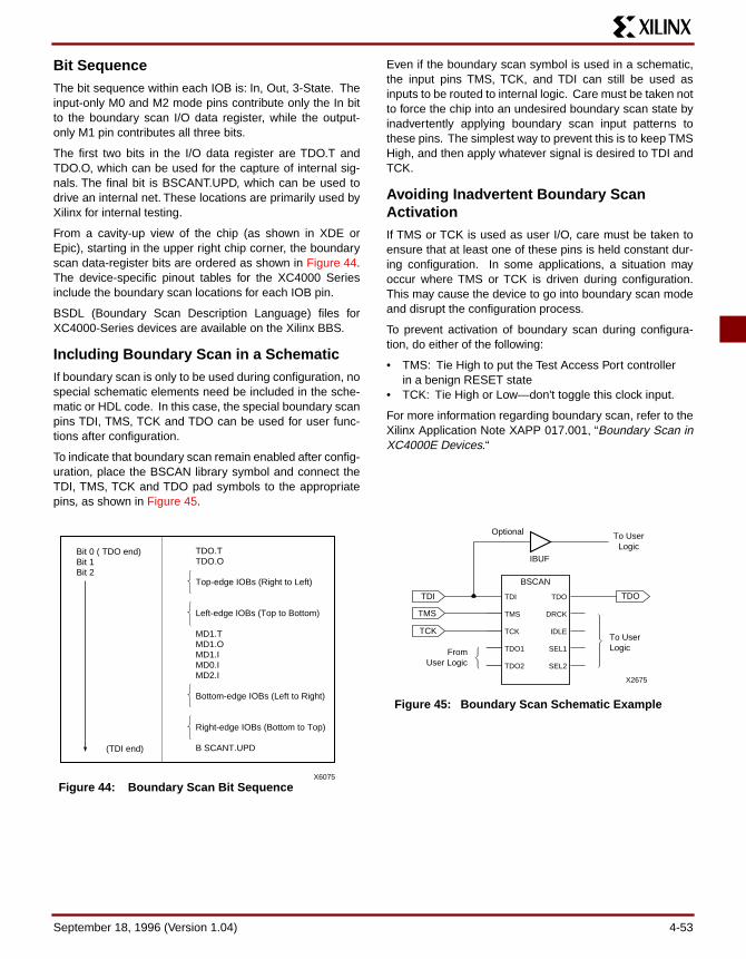
Bit Sequence The bit sequence within each IOB is: In, Out, 3-State. Theinput-only M0 and M2 mode pins contribute only the In bitto the boundary scan I/O data register, while the output-only M1 pin contributes all three bits.
The first two bits in the I/O data register are TDO.T andTDO.O, which can be used for the capture of internal sig-nals. The final bit is BSCANT.UPD, which can be used todrive an internal net. These locations are primarily used byXilinx for internal testing.
From a cavity-up view of the chip (as shown in XDE orEpic), starting in the upper right chip corner, the boundaryscan data-register bits are ordered as shown in Figure 44.The device-specific pinout tables for the XC4000 Seriesinclude the boundary scan locations for each IOB pin.
BSDL (Boundary Scan Description Language) files forXC4000-Series devices are available on the Xilinx BBS.
Including Boundary Scan in a SchematicIf boundary scan is only to be used during configuration, nospecial schematic elements need be included in the sche-matic or HDL code. In this case, the special boundary scanpins TDI, TMS, TCK and TDO can be used for user func-tions after configuration.
To indicate that boundary scan remain enabled after config-uration, place the BSCAN library symbol and connect theTDI, TMS, TCK and TDO pad symbols to the appropriatepins, as shown in Figure 45.
Even if the boundary scan symbol is used in a schematic,the input pins TMS, TCK, and TDI can still be used asinputs to be routed to internal logic. Care must be taken notto force the chip into an undesired boundary scan state byinadvertently applying boundary scan input patterns tothese pins. The simplest way to prevent this is to keep TMSHigh, and then apply whatever signal is desired to TDI andTCK.
Avoiding Inadvertent Boundary Scan ActivationIf TMS or TCK is used as user I/O, care must be taken toensure that at least one of these pins is held constant dur-ing configuration. In some applications, a situation mayoccur where TMS or TCK is driven during configuration.This may cause the device to go into boundary scan modeand disrupt the configuration process.
To prevent activation of boundary scan during configura-tion, do either of the following:
• TMS: Tie High to put the Test Access Port controllerin a benign RESET state
• TCK: Tie High or Low—don't toggle this clock input.
For more information regarding boundary scan, refer to theXilinx Application Note XAPP 017.001, “Boundary Scan inXC4000E Devices.“
Bit 0 ( TDO end) Bit 1 Bit 2
TDO.T TDO.O Top-edge IOBs (Right to Left) Left-edge IOBs (Top to Bottom) MD1.T MD1.O MD1.I MD0.I MD2.I Bottom-edge IOBs (Left to Right) Right-edge IOBs (Bottom to Top) B SCANT.UPD(TDI end)
X6075
Figure 44: Boundary Scan Bit Sequence
TDI TMS TCK TDO1 TDO2
TDO
DRCK
IDLE
SEL1
SEL2
TDI
TMS
TCK
TDO
BSCAN
To User Logic
IBUF
Optional
From User Logic
To User Logic
X2675
Figure 45: Boundary Scan Schematic Example
September 18, 1996 (Version 1.04) 4-53

XC4000 Series Field Programmable Gate Arrays
Configuration Configuration is the process of loading design-specific pro-gramming data into one or more FPGAs to define the func-tional operation of the internal blocks and theirinterconnections. This is somewhat like loading the com-mand registers of a programmable peripheral chip.XC4000-Series devices use several hundred bits of config-uration data per CLB and its associated interconnects.Each configuration bit defines the state of a static memorycell that controls either a function look-up table bit, a multi-plexer input, or an interconnect pass transistor. The XACT-step development system translates the design into anetlist file. It automatically partitions, places and routes thelogic and generates the configuration data in PROM format.
Special Purpose Pins Three configuration mode pins (M2, M1, M0) are sampledprior to configuration to determine the configuration mode.After configuration, these pins can be used as auxiliaryconnections. M2 and M0 can be used as inputs, and M1can be used as an output. The XACTstep developmentsystem does not use these resources unless they areexplicitly specified in the design entry. This is done by plac-ing a special pad symbol called MD2, MD1, or MD0 insteadof the input or output pad symbol.
In XC4000-Series devices, the mode pins have weak pull-up resistors during configuration. With all three mode pinsHigh, Slave Serial mode is selected, which is the most pop-ular configuration mode. Therefore, for the most commonconfiguration mode, the mode pins can be left uncon-nected. (Note, however, that the internal pull-up resistorvalue can be as high as 100 kΩ.) After configuration, thesepins can individually have weak pull-up or pull-down resis-tors, as specified in the design. A pull-down resistor valueof 4.7 kΩ is recommended.
These pins are located in the lower left chip corner and arenear the readback nets. This location allows convenientrouting if compatibility with the XC2000 and XC3000 familyconventions of M0/RT, M1/RD is desired.
Configuration Modes XC4000E devices have six configuration modes.XC4000EX devices have the same six modes, plus anadditional configuration mode. These modes are selectedby a 3-bit input code applied to the M2, M1, and M0 inputs.There are three self-loading Master modes, two Peripheralmodes, and a Serial Slave mode, which is used primarilyfor daisy-chained devices. The seventh mode, calledExpress mode, is an additional slave mode that allowshigh-speed parallel configuration of the high-capacityXC4000EX devices. The coding for mode selection isshown in Table 20.
Note: * Peripheral Synchronous can be considered byte-wide Slave Parallel
A detailed description of each configuration mode, with tim-ing information, is included later in this data sheet. Duringconfiguration, some of the I/O pins are used temporarily forthe configuration process. All pins used during configura-tion are shown in Table 24 on page 78.
Master Modes
The three Master modes use an internal oscillator to gener-ate a Configuration Clock (CCLK) for driving potential slavedevices. They also generate address and timing for exter-nal PROM(s) containing the configuration data.
Master Parallel (Up or Down) modes generate the CCLKsignal and PROM addresses and receive byte parallel data.The data is internally serialized into the FPGA data-frameformat. The up and down selection generates startingaddresses at either zero or 3FFFF, for compatibility with dif-ferent microprocessor addressing conventions. The MasterSerial mode generates CCLK and receives the configura-tion data in serial form from a Xilinx serial-configurationPROM.
CCLK speed is selectable as either 1 MHz (default) or 8MHz (up to 10% lower for low-voltage devices). Configura-tion always starts at the default slow frequency, then canswitch to the higher frequency during the first frame. Fre-quency tolerance is -50% to +25%.
Peripheral Modes
The two Peripheral modes accept byte-wide data from abus. A RDY/BUSY status is available as a handshake sig-nal. In Asynchronous Peripheral mode, the internal oscilla-tor generates a CCLK burst signal that serializes the byte-wide data. CCLK can also drive slave devices. In the syn-
Table 20: Configuration Modes
Mode M2 M1 M0 CCLK DataMaster Serial 0 0 0 output Bit-SerialSlave Serial 1 1 1 input Bit-SerialMaster Parallel Up
1 0 0 output Byte-Wide, increment
from 00000 Master Parallel Down
1 1 0 output Byte-Wide, decrement from 3FFFF
Peripheral Synchronous*
0 1 1 input Byte-Wide
Peripheral Asynchronous
1 0 1 output Byte-Wide
Express(XC4000EX only)
0 1 0 input Byte-Wide
Reserved 0 0 1 — —
4-54 September 18, 1996 (Version 1.04)

chronous mode, an externally supplied clock input to CCLKserializes the data.
Slave Serial Mode
In Slave Serial mode, the FPGA receives serial configura-tion data on the rising edge of CCLK and, after loading itsconfiguration, passes additional data out, resynchronizedon the next falling edge of CCLK.
Multiple slave devices with identical configurations can bewired with parallel DIN inputs. In this way, multiple devicescan be configured simultaneously.
Serial Daisy Chain
Multiple devices with different configurations can be con-nected together in a “daisy chain,” and a single combinedbitstream used to configure the chain of slave devices.
To configure a daisy chain of devices, wire the CCLK pinsof all devices in parallel, as shown in Figure 55 on page 68.Connect the DOUT of each device to the DIN of the next.The lead or master FPGA and following slaves eachpasses resynchronized configuration data coming from asingle source. The header data, including the length count,is passed through and is captured by each FPGA when itrecognizes the 0010 preamble. Following the length-countdata, each FPGA outputs a High on DOUT until it hasreceived its required number of data frames.
After an FPGA has received its configuration data, itpasses on any additional frame start bits and configurationdata on DOUT. When the total number of configurationclocks applied after memory initialization equals the valueof the 24-bit length count, the FPGAs begin the start-upsequence and become operational together. FPGA I/O arenormally released two CCLK cycles after the last configura-tion bit is received. Figure 49 on page 61 shows the start-up timing for an XC4000-Series device.
The daisy-chained bitstream is not simply a concatenationof the individual bitstreams. The MakePROM programmust be used to combine the bitstreams for a daisy-chained configuration.
Multi-Family Daisy Chain
All Xilinx FPGAs of the XC2000, XC3000, and XC4000Series use a compatible bitstream format and can, there-fore, be connected in a daisy chain in an arbitrarysequence. There is, however, one limitation. The leaddevice must belong to the highest family in the chain. If thechain contains XC4000-Series devices, the master nor-mally cannot be an XC2000 or XC3000 device.
The reason for this rule is shown in Figure 49 on page 61.Since all devices in the chain store the same length countvalue and generate or receive one common sequence ofCCLK pulses, they all recognize length-count match on thesame CCLK edge, as indicated on the left edge ofFigure 49. The master device then generates additional
CCLK pulses until it reaches its finish point F. The differentfamilies generate or require different numbers of additionalCCLK pulses until they reach F. Not reaching F means thatthe device does not really finish its configuration, althoughDONE may have gone High, the outputs became active,and the internal reset was released. For the XC4000-Series device, not reaching F means that readback cannotbe initiated and most boundary scan instructions cannot beused.
The user has some control over the relative timing of theseevents and can, therefore, make sure that they occur at theproper time and the finish point F is reached. Timing is con-trolled using MakeBits options.
XC3000 Master with an XC4000-Series Slave
Some designers want to use an inexpensive lead device inperipheral mode and have the more precious I/O pins of theXC4000-Series devices all available for user I/O. Figure 46provides a solution for that case.
This solution requires one CLB, one IOB and pin, and aninternal oscillator with a frequency of up to 5 MHz as aclock source. The XC3000 master device must be config-ured with late Internal Reset, which is the default option.
One CLB and one IOB in the lead XC3000-family deviceare used to generate the additional CCLK pulse required bythe XC4000-Series devices. When the lead deviceremoves the internal RESET signal, the 2-bit shift registerresponds to its clock input and generates an active Lowoutput signal for the duration of the subsequent clockperiod. An external connection between this output andCCLK thus creates the extra CCLK pulse.
Express Mode (XC4000EX only)
Express mode is similar to Slave Serial mode, except thedata is presented in parallel format, and is clocked into thetarget device a byte at a time rather than a bit at a time. Thedata is loaded in parallel into eight different columns: it isnot internally serialized. Eight bits of configuration data areloaded with every CCLK cycle, therefore this configuration
Output Connected to CCLK
OE/T
0 1 1 0 0 . .
0 0 1 1 1 . .
Reset
X5223etc
Active Low Output Active High Output
Figure 46: CCLK Generation for XC3000 Master Driving an XC4000-Series Slave
September 18, 1996 (Version 1.04) 4-55

XC4000 Series Field Programmable Gate Arrays
mode runs at eight times the data rate of the other sixmodes. A length count is not used in Express mode.
Express mode must be specified as an option to the Make-Bits program, which generates the bitstream. The Expressmode bitstream is not compatible with the other six config-uration modes.
Multiple slave devices with identical configurations can bewired with parallel D0-D7 inputs. In this way, multipledevices can be configured simultaneously.
Pseudo Daisy Chain
Multiple devices with different configurations can be con-nected together in a pseudo daisy chain, provided that all ofthe devices are in Express mode. A single combined bit-stream is used to configure the chain of Express modedevices, but the input data bus must drive D0-D7 of eachdevice. Tie High the CS1 pin of the first device to be con-figured. Connect the DOUT pin of each FPGA to the CS1pin of the next device in the chain. The D0-D7 inputs arewired to each device in parallel. The DONE pins are wiredtogether, with one or more internal DONE pull-ups acti-vated. Alternatively, a 4.7 kΩ external resistor can be used,if desired. (See Figure 63 on page 76.)
The requirement that all DONE pins in a daisy chain bewired together applies only to Express mode, and only if alldevices in the chain are to become active simultaneously.All XC4000EX devices in Express mode are synchronizedto the DONE pin. User I/O for each device become activeafter the DONE pin for that device goes High. (The exacttiming is determined by MakeBits options.) Since theDONE pin is open-drain and does not drive a High value,tying the DONE pins of all devices together prevents alldevices in the chain from going High until the last device inthe chain has completed its configuration cycle.
Because only XC4000EX and XC5200 devices supportExpress mode, only these devices can be used to form anExpress mode daisy chain. XC5200 devices used in acombined daisy chain with XC4000EX devices should beconfigured as synchronized to DONE (MakeBits optionCCLK_SYNC or UCLK_SYNC), and their DONE pins wiredtogether with those of the XC4000EX devices.
Setting CCLK FrequencyFor Master modes, CCLK can be generated in either of twofrequencies. In the default slow mode, the frequencyranges from 0.5 MHz to 1.25 MHz (up to 10% lower for low-voltage devices). In fast CCLK mode, the frequency rangesfrom 4 MHz to 10 MHz (up to 10% lower for low-voltagedevices). The frequency is selected by an option when run-ning MakeBits, the bitstream generation software tool. If anXC4000-Series Master is driving an XC3000- or XC2000-family slave, slow CCLK mode must be used. Slow mode isthe default.
Data Stream Format The data stream (“bitstream”) format is identical for all con-figuration modes, with the exception of Express mode. InExpress mode, the device becomes active when DONEgoes High, therefore no length count is required. Addition-ally, CRC error checking is not supported in Express mode.
The data stream formats are shown in Table 21. Expressmode data is shown with D0 at the left and D7 at the right.For all other modes, bit-serial data is read from left to right,and byte-parallel data is effectively assembled from thisserial bitstream, with the first bit in each byte assigned toD0.
The configuration data stream begins with a string of eightones, a preamble code, followed by a 24-bit length countand a separator field of ones (or 24 fill bits, in Expressmode). This header is followed by the actual configurationdata in frames. The length and number of frames dependson the device type (see Table 22 and Table 23). Eachframe begins with a start field and ends with an error check.In all modes except Express mode, a postamble code isrequired to signal the end of data for a single device. In allcases, additional start-up bytes of data are required to pro-vide four clocks for the startup sequence at the end of con-figuration. Long daisy chains require additional startupbytes to shift the last data through the chain. All startupbytes are don’t-cares; these bytes are not included in bit-streams created by the Xilinx software.
Table 21: XC4000-Series Data Stream Formats
LEGEND:
Data TypeExpress Mode
(D0-D7)All Other
Modes (D0...)Fill Byte 11111111b 11111111bPreamble Code 11110010b 0010bLength Count FFFFFFh COUNT(23:0)Fill Bits — 1111bStart Field 11010010b 0bData Frame DATA(n-1:0) DATA(n-1:0)CRC or Constant Field Check
11010010b xxxx (CRC)or 0110b
Extend Write Cycle FFFFFFFFFFh —Postamble — 01111111bStart-Up Bytes xxxxxxxxh xxh
Unshaded Once per bitstream
Light Once per data frame
Dark Once per device
4-56 September 18, 1996 (Version 1.04)

Notes: 1. Bits per Frame = (10 x number of rows) + 7 for the top + 13 for the bottom + 1 + 1 start bit + 4 error check bitsNumber of Frames = (36 x number of columns) + 26 for the left edge + 41 for the right edge + 1Program Data = (Bits per Frame x Number of Frames) + 8 postamble bitsPROM Size = Program Data + 40
2. The user can add more “one” bits as leading dummy bits in the header, or, if CRC = off, as trailing dummy bits at the end of any frame, following the four error check bits. However, the Length Count value must be adjusted for all such extra “one” bits, even for extra leading ones at the beginning of the header.
The MakeBits software creates the configuration bitstream.In Express mode, only non-CRC error checking is sup-ported. In all other modes, MakeBits allows a selection ofCRC or non-CRC error checking. The non-CRC errorchecking tests for a designated end-of-frame field for eachframe. For CRC error checking, MakeBits calculates a run-ning CRC and inserts a unique four-bit partial check at theend of each frame. The 11-bit CRC check of the last frameof an FPGA includes the last seven data bits.
Detection of an error results in the suspension of data load-ing and the pulling down of the INIT pin. In Master modes,CCLK and address signals continue to operate externally.The user must detect INIT and initialize a new configurationby pulsing the PROGRAM pin Low or cycling Vcc.
Cyclic Redundancy Check (CRC) for Configuration and ReadbackThe Cyclic Redundancy Check is a method of error detec-tion in data transmission applications. Generally, the trans-mitting system performs a calculation on the serialbitstream. The result of this calculation is tagged onto thedata stream as additional check bits. The receiving system
performs an identical calculation on the bitstream and com-pares the result with the received checksum.
Each data frame of the configuration bitstream has fourerror bits at the end, as shown in Table 21. If a frame dataerror is detected during the loading of the FPGA, the con-figuration process with a potentially corrupted bitstream isterminated. The FPGA pulls the INIT pin Low and goes intoa Wait state.
During Readback, 11 bits of the 16-bit checksum are addedto the end of the Readback data stream. The checksum iscomputed using the CRC-16 CCITT polynomial, as shownin Figure 47. The checksum consists of the 11 most signif-icant bits of the 16-bit code. A change in the checksumindicates a change in the Readback bitstream. A compari-son to a previous checksum is meaningful only if the read-back data is independent of the current device state. CLBoutputs should not be included (Read Capture MakeBitsoption not used), and if RAM is present, the RAM contentmust be unchanged.
Statistically, one error out of 2048 might go undetected.
Table 22: XC4000E Program Data
Device XC4003E XC4005E/L XC4006E XC4008E XC4010E/L XC4013E/L XC4020E XC4025EMax Logic Gates 3,000 5,000 6,000 8,000 10,000 13,000 20,000 25,000CLBs (Row x Col.)
100(10 x 10)
196(14 x 14)
256(16 x 16)
324(18 x 18)
400(20 x 20)
576(24 x 24)
784(28 x 28)
1,024(32 x 32)
IOBs 80 112 128 144 160 192 224 256Flip-Flops 360 616 768 936 1,120 1,536 2,016 2,560HorizontalLonglines
20 28 32 36 40 48 56 64
TBUFs per Longline
12 16 18 20 22 26 30 34
Bits per Frame 126 166 186 206 226 266 306 346Frames 428 572 644 716 788 932 1,076 1,220Program Data 53,936 94,960 119,792 147,504 178,096 247,920 329,264 422,128PROM Size (bits)
53,984 95,008 119,840 147,552 178,144 247,968 329,312 422,176
September 18, 1996 (Version 1.04) 4-57

XC4000 Series Field Programmable Gate Arrays
Notes: 1. Bits per Frame = (12 x number of rows) + 8 for the top + 16 for the bottom + 8 + 1 start bit + 4 error check bitsNumber of Frames = (47 x number of columns) + 27 for the left edge + 52 for the right edge + 4Program Data = (Bits per Frame x Number of Frames) + 8 postamble bitsPROM Size = Program Data + 40
2. The user can add more “one” bits as leading dummy bits in the header, or, if CRC = off, as trailing dummy bits at the end of any frame, following the four error check bits. However, the Length Count value must be adjusted for all such extra “one” bits, even for extra leading ones at the beginning of the header.
3. Express mode bitfiles are slightly larger (see Table 21).
Table 23: XC4000EX Program Data
Device XC4028EX/XL XC4036EX/XL XC4044EX/XL XC4052XL XC4062XLMax Logic Gates 28,000 36,000 44,000 52,000 62,000CLBs (Row x Col.)
1,024(32 x 32)
1,296(36 x 36)
1,600(40 x 40)
1,936(44 x 44)
2,304(48 x 48)
IOBs 256 288 320 352 384Flip-Flops 2,560 3,168 3,840 4,576 5,376Horizontal Longlines 192 216 240 264 288TBUFs per Longline 34 38 42 46 50Bits per Frame 421 469 517 565 613Frames 1587 1775 1963 2151 2,339Program Data 668,127 832,483 1,014,879 1,215,323 1,433,807PROM Size (bits) 668,167 832,523 1,014,919 1,215,363 1,433,847
0
X2
2 3 4 5 6 7 8 9 10 11 12 13 141
X15X16
15
SERIAL DATA IN
1 0 15 14 13 12 11 10 9 8 7 6 51111
CRC – CHECKSUMLAST DATA FRAME
ST
AR
T B
IT
X1789
Polynomial: X16 + X15 + X2 + 1
Readback Data Stream
Figure 47: Circuit for Generating CRC-16
4-58 September 18, 1996 (Version 1.04)

Configuration Sequence There are four major steps in the XC4000-Series power-upconfiguration sequence.
• Configuration Memory Clear• Initialization• Configuration• Start-Up
The full process is illustrated in Figure 48.
Configuration Memory Clear
When power is first applied or is reapplied to an FPGA, aninternal circuit forces initialization of the configuration logic.When Vcc reaches an operational level, and the circuitpasses the write and read test of a sample pair of configu-ration bits, a time delay is started. This time delay is nomi-nally 16 ms, and up to 10% longer in the low-voltagedevices. The delay is four times as long when in MasterModes (M0 Low), to allow ample time for all slaves to reacha stable Vcc. When all INIT pins are tied together, as rec-ommended, the longest delay takes precedence. There-fore, devices with different time delays can easily be mixedand matched in a daisy chain.
This delay is applied only on power-up. It is not appliedwhen reconfiguring an FPGA by pulsing the PROGRAM pinLow. During this time delay, or as long as the PROGRAMinput is asserted, the configuration logic is held in a Config-uration Memory Clear state. The configuration-memoryframes are consecutively initialized, using the internal oscil-lator.
At the end of each complete pass through the frameaddressing, the power-on time-out delay circuitry and thelevel of the PROGRAM pin are tested. If neither isasserted, the logic initiates one additional clearing of theconfiguration frames and then tests the INIT input.
Initialization
During initialization and configuration, user pins HDC, LDC,INIT and DONE provide status outputs for the system inter-face. The outputs LDC, INIT and DONE are held Low andHDC is held High starting at the initial application of power.
The open drain INIT pin is released after the final initializa-tion pass through the frame addresses. There is a deliber-ate delay of 50 to 250 µs (up to 10% longer for low-voltagedevices) before a Master-mode device recognizes an inac-tive INIT. Two internal clocks after the INIT pin is recognizedas High, the FPGA samples the three mode lines to deter-mine the configuration mode. The appropriate interfacelines become active and the configuration preamble anddata can be loaded.
INIT High? if Master
Sample Mode Lines
Load One Configuration Data Frame
Frame Error
Pass Configuration
Data to DOUT
VCC >3.5 V
No
Yes
Yes
No
No
Yes
Operational
Start-Up Sequence
No
Yes
~1.3 µs per Frame
Master Waits 50 to 250 µs Before Sampling Mode Lines
Master CCLK Goes Active
F
Pull INIT Low and Stop
X6076
EXTEST* SAMPLE/PRELOAD
BYPASS CONFIGURE*
(* if PROGRAM = High)
SAMPLE/PRELOAD BYPASS
EXTEST SAMPLE PRELOAD
BYPASS USER 1 USER 2
CONFIGURE READBACK
If Boundary Scan is Selected
Config- uration memory
Full
CCLK Count Equals
Length Count
Completely Clear Configuration Memory
Once More
LDC
Out
put =
L, H
DC
Out
put =
H
Boundary Scan Instructions Available:
I/O A
ctiv
e
Keep Clearing Configuration Memory
Test M0 Generate One Time-Out Pulse
of 16 or 64 ms
PROGRAM = Low
No
Yes
Yes
Figure 48: Power-up Configuration Sequence
September 18, 1996 (Version 1.04) 4-59

XC4000 Series Field Programmable Gate Arrays
Configuration
The 0010 preamble code, included for all modes exceptExpress mode, indicates that the following 24 bits repre-sent the length count. The length count is the total numberof configuration clocks needed to load the complete config-uration data. (Four additional configuration clocks arerequired to complete the configuration process, as dis-cussed below.) After the preamble and the length counthave been passed through to all devices in the daisy chain,DOUT is held High to prevent frame start bits from reachingany daisy-chained devices. In Express mode, the lengthcount bits are ignored, and DOUT is held Low, to disablethe next device in the pseudo daisy chain.
A specific configuration bit, early in the first frame of a mas-ter device, controls the configuration-clock rate and canincrease it by a factor of eight. Therefore, if a fast configu-ration clock is selected by the bitstream, the slower clockrate is used until this configuration bit is detected.
Each frame has a start field followed by the frame-configu-ration data bits and a frame error field. If a frame data erroris detected, the FPGA halts loading, and signals the errorby pulling the open-drain INIT pin Low. After all configura-tion frames have been loaded into an FPGA, DOUT againfollows the input data so that the remaining data is passedon to the next device. In Express mode, when the firstdevice is fully programmed, DOUT goes High to enable thenext device in the chain.
Delaying Configuration After Power-Up
There are two methods of delaying configuration afterpower-up: put a logic Low on the PROGRAM input, or pullthe bidirectional INIT pin Low, using an open-collector(open-drain) driver. (See Figure 48 on page 59.)
A Low on the PROGRAM input is the more radicalapproach, and is recommended when the power-supplyrise time is excessive or poorly defined. As long as PRO-GRAM is Low, the FPGA keeps clearing its configurationmemory. When PROGRAM goes High, the configurationmemory is cleared one more time, followed by the begin-ning of configuration, provided the INIT input is not exter-nally held Low. Note that a Low on the PROGRAM inputautomatically forces a Low on the INIT output. TheXC4000-Series PROGRAM pin has a permanent weakpull-up.
Using an open-collector or open-drain driver to hold INITLow before the beginning of configuration causes theFPGA to wait after completing the configuration memoryclear operation. When INIT is no longer held Low exter-nally, the device determines its configuration mode by cap-turing its mode pins, and is ready to start the configurationprocess. A master device waits up to an additional 250 µs
to make sure that any slaves in the optional daisy chainhave seen that INIT is High.
Start-Up
Start-up is the transition from the configuration process tothe intended user operation. This transition involves achange from one clock source to another, and a changefrom interfacing parallel or serial configuration data wheremost outputs are 3-stated, to normal operation with I/O pinsactive in the user-system. Start-up must make sure that theuser-logic ‘wakes up’ gracefully, that the outputs becomeactive without causing contention with the configuration sig-nals, and that the internal flip-flops are released from theglobal Reset or Set at the right time.
Figure 49 describes start-up timing for the three Xilinx fam-ilies in detail. Express mode configuration always useseither CCLK_SYNC or UCLK_SYNC timing, the other con-figuration modes can use any of the four timing sequences.
To access the internal start-up signals, place the STARTUPlibrary symbol.
Start-up Timing
Different FPGA families have different start-up sequences.
The XC2000 family goes through a fixed sequence. DONEgoes High and the internal global Reset is de-activated oneCCLK period after the I/O become active.
The XC3000A family offers some flexibility. DONE can beprogrammed to go High one CCLK period before or afterthe I/O become active. Independent of DONE, the internalglobal Reset is de-activated one CCLK period before orafter the I/O become active.
The XC4000 Series offers additional flexibility. The threeevents — DONE going High, the internal Set/Reset beingde-activated, and the user I/O going active — can all occurin any arbitrary sequence. Each of them can occur oneCCLK period before or after, or simultaneous with, any ofthe others. This relative timing is selected by means of soft-ware options in MakeBits, the bitstream generation soft-ware.
The default option, and the most practical one, is for DONEto go High first, disconnecting the configuration data sourceand avoiding any contention when the I/Os become activeone clock later. Reset/Set is then released another clockperiod later to make sure that user-operation starts fromstable internal conditions. This is the most commonsequence, shown with heavy lines in Figure 49, but thedesigner can modify it to meet particular requirements.
Normally, the start-up sequence is controlled by the internaldevice oscillator output (CCLK), which is asynchronous tothe system clock.
4-60 September 18, 1996 (Version 1.04)
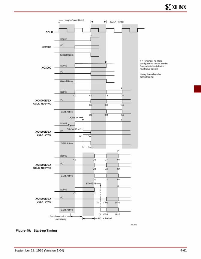
XC4000E/EX UCLK_SYNC
XC4000E/EX UCLK_NOSYNC
XC4000E/EX CCLK_SYNC
XC4000E/EX CCLK_NOSYNC
XC3000
XC2000
CCLK
GSR Active
UCLK Period
DONE IN
DONE IN
Di Di+1 Di+2
Di Di+1 Di+2
U2 U3 U4
U2 U3 U4
U2 U3 U4C1
Synchronization Uncertainty
Di Di+1
Di Di+1
DONE
I/O
GSR Active
DONE
I/O
GSR Active
DONE
C1 C2
C1 U2
C3 C4
C2 C3 C4
C2 C3 C4
I/O
GSR Active
DONE
I/O
DONE
Global Reset
I/O
DONE
Global Reset
I/O
F = Finished, no more configuration clocks needed Daisy-chain lead device must have latest F Heavy lines describe default timing
CCLK PeriodLength Count Match
F
F
F
F
F
F
X6700
C1, C2 or C3
Figure 49: Start-up Timing
September 18, 1996 (Version 1.04) 4-61

XC4000 Series Field Programmable Gate Arrays
The XC4000 Series offers another start-up clocking option,UCLK_NOSYNC. The three events described above neednot be triggered by CCLK. They can, as a configurationoption, be triggered by a user clock. This means that thedevice can wake up in synchronism with the user system.
When the UCLK_SYNC option is enabled, the user canexternally hold the open-drain DONE output Low, and thusstall all further progress in the start-up sequence untilDONE is released and has gone High. This option can beused to force synchronization of several FPGAs to a com-mon user clock, or to guarantee that all devices are suc-cessfully configured before any I/Os go active.
If either of these two options is selected, and no user clockis specified in the design or attached to the device, the chipcould reach a point where the configuration of the device iscomplete and the Done pin is asserted, but the outputs donot become active. The solution is either to recreate the bit-stream specifying the start-up clock as CCLK, or to supplythe appropriate user clock.
Start-up Sequence
The Start-up sequence begins when the configurationmemory is full, and the total number of configuration clocksreceived since INIT went High equals the loaded value ofthe length count.
The next rising clock edge sets a flip-flop Q0, shown inFigure 50. Q0 is the leading bit of a 5-bit shift register. Theoutputs of this register can be programmed to control threeevents.
• The release of the open-drain DONE output• The change of configuration-related pins to the user
function, activating all IOBs. • The termination of the global Set/Reset initialization of
all CLB and IOB storage elements.
The DONE pin can also be wire-ANDed with DONE pins ofother FPGAs or with other external signals, and can thenbe used as input to bit Q3 of the start-up register. This iscalled “Start-up Timing Synchronous to Done In” and isselected by the CCLK_SYNC and UCLK_SYNC MakeBitsoptions.
When DONE is not used as an input, the operation is called“Start-up Timing Not Synchronous to DONE In,” and isselected by the CCLK_NOSYNC and UCLK_NOSYNCMakeBits options.
As a configuration option, the start-up control registerbeyond Q0 can be clocked either by subsequent CCLKpulses or from an on-chip user net called STARTUP.CLK.These signals can be accessed by placing the STARTUPlibrary symbol.
Start-up from CCLK
If CCLK is used to drive the start-up, Q0 through Q3 pro-vide the timing. Heavy lines in Figure 49 show the defaulttiming, which is compatible with XC2000 and XC3000devices using early DONE and late Reset. The thin linesindicate all other possible timing options.
Start-up from a User Clock (STARTUP.CLK)
When, instead of CCLK, a user-supplied start-up clock isselected, Q1 is used to bridge the unknown phase relation-ship between CCLK and the user clock. This arbitrationcauses an unavoidable one-cycle uncertainty in the timingof the rest of the start-up sequence.
DONE Goes High to Signal End of Configuration
In all configuration modes except Express mode, XC4000-Series devices read the expected length count from the bit-stream and store it in an internal register. The length countvaries according to the number of devices and the compo-sition of the daisy chain. Each device also counts the num-ber of CCLKs during configuration.
Two conditions have to be met in order for the DONE pin togo high:
• the chip's internal memory must be full, and• the configuration length count must be met, exactly.
This is important because the counter that determineswhen the length count is met begins with the very firstCCLK, not the first one after the preamble.
Therefore, if a stray bit is inserted before the preamble, orthe data source is not ready at the time of the first CCLK,the internal counter that holds the number of CCLKs will beone ahead of the actual number of data bits read. At theend of configuration, the configuration memory will be full,but the number of bits in the internal counter will not matchthe expected length count.
As a consequence, a Master mode device will continue tosend out CCLKs until the internal counter turns over tozero, and then reaches the correct length count a secondtime. This will take several seconds [224 ∗ CCLK period] —which is sometimes interpreted as the device not configur-ing at all.
If it is not possible to have the data ready at the time of thefirst CCLK, the problem can be avoided by increasing thenumber in the length count by the appropriate value. TheXACT User Guide includes detailed information about man-ually altering the length count.
In Express mode, there is no length count. The DONE pinfor each device goes High when the device has received itsquota of configuration data. Wiring the DONE pins of sev-eral devices together delays start-up of all devices until allare fully configured.
4-62 September 18, 1996 (Version 1.04)

Note that DONE is an open-drain output and does not goHigh unless an internal pull-up is activated or an externalpull-up is attached. The internal pull-up is activated as thedefault by MakeBits, the bitstream generation software.
Release of User I/O After DONE Goes High
By default, the user I/O are released one CCLK cycle afterthe DONE pin goes High. If CCLK is not clocked afterDONE goes High, the outputs remain in their initial state —3-stated, with a 50 kΩ - 100 kΩ pull-up. The delay fromDONE High to active user I/O is controlled by a MakeBitsoption.
Release of Global Set/Reset After DONE Goes High
By default, Global Set/Reset (GSR) is released two CCLKcycles after the DONE pin goes High. If CCLK is notclocked twice after DONE goes High, all flip-flops are heldin their initial set or reset state. The delay from DONE Highto GSR inactive is controlled by a MakeBits option.
Configuration Complete After DONE Goes High
Three full CCLK cycles are required after the DONE pingoes High, as shown in Figure 49 on page 61. If CCLK isnot clocked three times after DONE goes High, readbackcannot be initiated and most boundary scan instructionscannot be used.
DONE
*
*
*
*
* *
Q S
R
1
0
0
1
1
0
1
0
1
0
0
1
GSR ENABLEGSR INVERTSTARTUP.GSR
STARTUP.GTSGTS INVERTGTS ENABLE
CONTROLLED BY STARTUP SYMBOL IN THE USER SCHEMATIC (SEE LIBRARIES GUIDE)
GLOBAL SET/RESET OF ALL CLB AND IOB FLIP-FLOP
IOBs OPERATIONAL PER CONFIGURATION
GLOBAL 3-STATE OF ALL IOBs
Q2
Q3 Q1/Q4DONE IN
STARTUP
Q0 Q1 Q2 Q3 Q4
M
M
" FINISHED " ENABLES BOUNDARY SCAN, READBACK AND CONTROLS THE OSCILLATOR
K
S Q
K
D Q
K
D Q
K
D Q
K
D QFULL
LENGTH COUNT
CLEAR MEMORY
CCLK
STARTUP.CLK USER NET
CONFIGURATION BIT OPTIONS SELECTED BY USER IN "MAKEBITS"X1528
Figure 50: Start-up Logic
September 18, 1996 (Version 1.04) 4-63

XC4000 Series Field Programmable Gate Arrays
Configuration Through the Boundary Scan PinsXC4000-Series devices can be configured through theboundary scan pins. The basic procedure is as follows:
• Power up the FPGA with INIT held Low (or drive the PROGRAM pin Low for more than 300 ns followed by a High while holding INIT Low). Holding INIT Low allows enough time to issue the CONFIG command to the FPGA. The pin can be used as I/O after configuration if a resistor is used to hold INIT Low.
• Issue the CONFIG command to the TMS input• Wait for INIT to go High • Sequence the boundary scan Test Access Port to the
SHIFT-DR state• Toggle TCK to clock data into TDI pin.
The user must account for all TCK clock cycles after INITgoes High, as all of these cycles affect the Length Countcompare.
For more detailed information, refer to the Xilinx applicationnote XAPP017, “Boundary Scan in XC4000 Devices.” Thisapplication note also applies to XC4000E and XC4000EXdevices.
Readback The user can read back the content of configuration mem-ory and the level of certain internal nodes without interfer-ing with the normal operation of the device.
Readback not only reports the downloaded configurationbits, but can also include the present state of the device,represented by the content of all flip-flops and latches inCLBs and IOBs, as well as the content of function genera-tors used as RAMs.
Note that in XC4000-Series devices, configuration data isnot inverted with respect to configuration as it is in XC2000and XC3000 families.
Readback of Express mode bitstreams results in data thatdoes not resemble the original bitstream, because the bit-stream format differs from other modes.
XC4000-Series Readback does not use any dedicatedpins, but uses four internal nets (RDBK.TRIG, RDBK.DATA,RDBK.RIP and RDBK.CLK) that can be routed to any IOB.To access the internal Readback signals, place the READ-BACK library symbol and attach the appropriate pad sym-bols, as shown in Figure 51.
After Readback has been initiated by a Low-to-High transi-tion on RDBK.TRIG, the RDBK.RIP (Read In Progress)output goes High on the next rising edge of RDBK.CLK.Subsequent rising edges of this clock shift out Readbackdata on the RDBK.DATA net.
Readback data does not include the preamble, but startswith five dummy bits (all High) followed by the Start bit(Low) of the first frame. The first two data bits of the firstframe are always High.
Each frame ends with four error check bits. They are readback as High. The last seven bits of the last frame are alsoread back as High. An additional Start bit (Low) and an11-bit Cyclic Redundancy Check (CRC) signature follow,before RDBK.RIP returns Low.
READBACK
DATA
RIPTRIG
CLK READ_DATA
OBUF
MD1
MD0READ_TRIGGER
IBUF X1786
IF UNCONNECTED, DEFAULT IS CCLK
Figure 51: Readback Schematic Example
4-64 September 18, 1996 (Version 1.04)

Readback OptionsReadback options are: Read Capture, Read Abort, andClock Select. They are set with MakeBits, the bitstreamgeneration software.
Read Capture
When the Read Capture option is selected, the readbackdata stream includes sampled values of CLB and IOB sig-nals. The rising edge of RDBK.TRIG latches the invertedvalues of the four CLB outputs, the IOB output flip-flops andthe input signals I1 and I2. Note that while the bits describ-ing configuration (interconnect, function generators, andRAM content) are not inverted, the CLB and IOB output sig-nals are inverted.
When the Read Capture option is not selected, the valuesof the capture bits reflect the configuration data originallywritten to those memory locations.
If the RAM capability of the CLBs is used, RAM data areavailable in readback, since they directly overwrite the Fand G function-table configuration of the CLB.
RDBK.TRIG is located in the lower-left corner of the device,as shown in Figure 52.
Read Abort
When the Read Abort option is selected, a High-to-Lowtransition on RDBK.TRIG terminates the readback opera-tion and prepares the logic to accept another trigger.
After an aborted readback, additional clocks (up to onereadback clock per configuration frame) may be required tore-initialize the control logic. The status of readback is indi-cated by the output control net RDBK.RIP. RDBK.RIP isHigh whenever a readback is in progress.
Clock Select
CCLK is the default clock. However, the user can insertanother clock on RDBK.CLK. Readback control and dataare clocked on rising edges of RDBK.CLK. If readbackmust be inhibited for security reasons, the readback controlnets are simply not connected.
RDBK.CLK is located in the lower right chip corner, asshown in Figure 52.
Violating the Maximum High and Low Time Specification for the Readback ClockThe readback clock has a maximum High and Low timespecification. In some cases, this specification cannot bemet. For example, if a processor is controlling readback, aninterrupt may force it to stop in the middle of a readback.This necessitates stopping the clock, and thus violating thespecification.
The specification is mandatory only on clocking data at theend of a frame prior to the next start bit. The transfer mech-anism will load the data to a shift register during the last sixclock cycles of the frame, prior to the start bit of the follow-ing frame. This loading process is dynamic, and is thesource of the maximum High and Low time requirements.
Therefore, the specification only applies to the six clockcycles prior to and including any start bit, including theclocks before the first start bit in the readback data stream.At other times, the frame data is already in the register andthe register is not dynamic. Thus, it can be shifted out justlike a regular shift register.
The user must precisely calculate the location of the read-back data relative to the frame. The system must keeptrack of the position within a data frame, and disable inter-rupts before frame boundaries. Frame lengths and dataformats are listed in Table 21, Table 22 and Table 23.
Readback with the XChecker CableThe XChecker Universal Download/Readback Cable andLogic Probe uses the readback feature for bitstream verifi-cation. It can also display selected internal signals on thePC or workstation screen, functioning as a low-cost in-cir-cuit emulator.
I/O I/O I/Ordbk
PROGRAMMABLE INTERCONNECT
rdclk
I/O I/O
X1787
TR
IGD
AT
AR
IP I
Figure 52: READBACK Symbol in Graphical Editor
September 18, 1996 (Version 1.04) 4-65

XC4000 Series Field Programmable Gate Arrays
Configuration TimingThe seven configuration modes are discussed in detail inthis section. Timing specifications are included.
Master Serial ModeIn Master Serial mode, the CCLK output of the lead FPGAdrives a Xilinx Serial PROM that feeds the FPGA DIN input.Each rising edge of the CCLK output increments the SerialPROM internal address counter. The next data bit is put onthe SPROM data output, connected to the FPGA DIN pin.The lead FPGA accepts this data on the subsequent risingCCLK edge.
The lead FPGA then presents the preamble data—and alldata that overflows the lead device—on its DOUT pin.There is an internal pipeline delay of 1.5 CCLK periods,which means that DOUT changes on the falling CCLKedge, and the next FPGA in the daisy chain accepts dataon the subsequent rising CCLK edge.
In MakeBits, the user can specify Fast ConfigRate, which,starting several bits into the first frame, increases the CCLKfrequency by a factor of eight. The value increases frombetween 0.5 and 1.25 MHz, to a value between 4 and 10MHz. (For low-voltage devices, the frequency can be up to10% lower.) Be sure that the serial PROM and slaves arefast enough to support this data rate. XC2000, XC3000/A,and XC3100A devices do not support the Fast ConfigRateoption.
The SPROM CE input can be driven from either LDC orDONE. Using LDC avoids potential contention on the DINpin, if this pin is configured as user-I/O, but LDC is thenrestricted to be a permanently High user output after con-figuration. Using DONE can also avoid contention on DIN,provided the early DONE option is invoked.
Figure 53 shows a full master/slave system. The leftmostdevice is in Master Serial mode.
Master Serial mode is selected by a <000> on the modepins (M2, M1, M0).
XC4000E/EX MASTER SERIAL
XC4000E/EX, XC5200 SLAVE
XC3100A SLAVE
XC1700D
PROGRAM
NOTE: M2, M1, M0 can be shorted to Ground if not used as I/O
NOTE: M2, M1, M0 can be shorted to VCC if not used as I/O
M2
M0 M1
DOUT
CCLK CLK
VCC
+5 V
DATA
CE CEO
VPP
RESET/OE DONE
DIN
LDC
INIT INITDONE
PROGRAM PROGRAM
D/P INIT
RESET
CCLK
DIN
CCLK
DINDOUT DOUT
M2M0 M1 M1 PWRDNM0
M2
(Low Reset Option Used)
4.7 KΩ
4.7 KΩ4.7 KΩ4.7 KΩ 4.7 KΩ4.7 KΩ4.7 KΩ
VCC
X6608
N/C
N/C
Figure 53: Master Serial Mode Circuit Diagram
4-66 September 18, 1996 (Version 1.04)

Notes: 1. At power-up, Vcc must rise from 2.0 V to Vcc min in less than 25 ms, otherwise delay configuration by pulling PROGRAM Low until Vcc is valid.
2. Master Serial mode timing is based on testing in slave mode.
Figure 54: Master Serial Mode Programming Switching Characteristics
Serial Data In
CCLK (Output)
Serial DOUT (Output)
1 TDSCK
2 TCKDS
n n + 1 n + 2
n – 3 n – 2 n – 1 n
X3223
Description Symbol Min Max Units
CCLKDIN setup 1 TDSCK 20 nsDIN hold 2 TCKDS 0 ns
September 18, 1996 (Version 1.04) 4-67

XC4000 Series Field Programmable Gate Arrays
Slave Serial ModeIn Slave Serial mode, an external signal drives the CCLKinput of the FPGA. The serial configuration bitstream mustbe available at the DIN input of the lead FPGA a short setuptime before each rising CCLK edge.
The lead FPGA then presents the preamble data—and alldata that overflows the lead device—on its DOUT pin.There is an internal delay of 0.5 CCLK periods, whichmeans that DOUT changes on the falling CCLK edge, and
the next FPGA in the daisy chain accepts data on the sub-sequent rising CCLK edge.
Figure 55 shows a full master/slave system. An XC4000-Series device in Slave Serial mode should be connected asshown in the third device from the left.
Slave Serial mode is selected by a <111> on the mode pins(M2, M1, M0). Slave Serial is the default mode if the modepins are left unconnected, as they have weak pull-up resis-tors during configuration.
XC4000E/EX MASTER SERIAL
XC4000E/EX, XC5200 SLAVE
XC3100A SLAVE
XC1700D
PROGRAM
NOTE: M2, M1, M0 can be shorted to Ground if not used as I/O
NOTE: M2, M1, M0 can be shorted to VCC if not used as I/O
M2
M0 M1
DOUT
CCLK CLK
VCC
+5 V
DATA
CE CEO
VPP
RESET/OE DONE
DIN
LDC
INIT INITDONE
PROGRAM PROGRAM
D/P INIT
RESET
CCLK
DIN
CCLK
DINDOUT DOUT
M2M0 M1 M1 PWRDNM0
M2
(Low Reset Option Used)
4.7 KΩ
4.7 KΩ4.7 KΩ4.7 KΩ 4.7 KΩ4.7 KΩ4.7 KΩ
VCC
X6608
N/C
N/C
Figure 55: Slave Serial Mode Circuit Diagram
4-68 September 18, 1996 (Version 1.04)

Note: Configuration must be delayed until the INIT pins of all daisy-chained FPGAs are High.
Figure 56: Slave Serial Mode Programming Switching Characteristics
4 TCCH
Bit n Bit n + 1
Bit nBit n - 1
3 TCCO
5 TCCL2 TCCD1 TDCC
DIN
CCLK
DOUT (Output)
X5379
Description Symbol Min Max Units
CCLK
DIN setup 1 TDCC 20 nsDIN hold 2 TCCD 0 nsDIN to DOUT 3 TCCO 30 nsHigh time 4 TCCH 45 nsLow time 5 TCCL 45 nsFrequency FCC 10 MHz
September 18, 1996 (Version 1.04) 4-69

XC4000 Series Field Programmable Gate Arrays
Master Parallel ModesIn the two Master Parallel modes, the lead FPGA directlyaddresses an industry-standard byte-wide EPROM, andaccepts eight data bits just before incrementing or decre-menting the address outputs.
The eight data bits are serialized in the lead FPGA, whichthen presents the preamble data—and all data that over-flows the lead device—on its DOUT pin. There is an inter-nal delay of 1.5 CCLK periods, after the rising CCLK edgethat accepts a byte of data (and also changes the EPROMaddress) until the falling CCLK edge that makes the LSB(D0) of this byte appear at DOUT. This means that DOUTchanges on the falling CCLK edge, and the next FPGA inthe daisy chain accepts data on the subsequent risingCCLK edge.
The PROM address pins can be incremented or decre-mented, depending on the mode pin settings. This optionallows the FPGA to share the PROM with a wide variety ofmicroprocessors and microcontrollers. Some processorsmust boot from the bottom of memory (all zeros) while oth-ers must boot from the top. The FPGA is flexible and canload its configuration bitstream from either end of the mem-ory.
Master Parallel Up mode is selected by a <100> on themode pins (M2, M1, M0). The EPROM addresses start at00000 and increment.
Master Parallel Down mode is selected by a <110> on themode pins. The EPROM addresses start at 3FFFF anddecrement.
M0 M1
DOUT
VCC
M2
PROGRAM
D7
D6
D5
D4
D3
D2
D1
D0
PROGRAM
CCLK
DIN
M0 M1 M2
DOUT
PROGRAM
EPROM (8K x 8)
(OR LARGER)
A10
A11
A12
A9
A8
A7
A6
A5
A4
A3
A2
A1
A0
D7
DONE
D6
D5
D4
D3
D2
D1
D0
N/C
N/C
CE
OE
XC4000E/EX SLAVE
8DATA BUS
CCLK
A15
A14
A13
A12
A11
A10
A9
A8
A7
A6
A5
A4
A3
A2
A1
A0
INIT
INIT
. . .
. . .
. . .USER CONTROL OF HIGHER ORDER PROM ADDRESS BITS CAN BE USED TO SELECT BETWEEN ALTERNATIVE CONFIGURATIONS
DONE
TO DIN OF OPTIONAL DAISY-CHAINED FPGAS
A16 . . .
A17 . . .
HIGH or
LOW
X6697
TO CCLK OF OPTIONAL DAISY-CHAINED FPGAS
4.7KΩ
4.7KΩ
NOTE:M0 can be shorted to Ground if not used as I/O.
Figure 57: Master Parallel Mode Circuit Diagram
4-70 September 18, 1996 (Version 1.04)
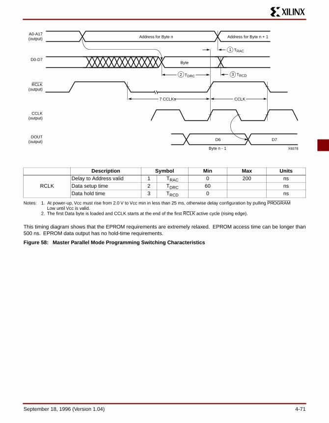
Notes: 1. At power-up, Vcc must rise from 2.0 V to Vcc min in less than 25 ms, otherwise delay configuration by pulling PROGRAM Low until Vcc is valid.
2. The first Data byte is loaded and CCLK starts at the end of the first RCLK active cycle (rising edge).
This timing diagram shows that the EPROM requirements are extremely relaxed. EPROM access time can be longer than500 ns. EPROM data output has no hold-time requirements.
Figure 58: Master Parallel Mode Programming Switching Characteristics
Address for Byte n
Byte
2 TDRC
Address for Byte n + 1
D7D6
A0-A17 (output)
D0-D7
RCLK (output)
CCLK (output)
DOUT (output)
1 TRAC
7 CCLKs CCLK
3 TRCD
Byte n - 1 X6078
Description Symbol Min Max Units
RCLKDelay to Address valid 1 TRAC 0 200 nsData setup time 2 TDRC 60 nsData hold time 3 TRCD 0 ns
September 18, 1996 (Version 1.04) 4-71

XC4000 Series Field Programmable Gate Arrays
Synchronous Peripheral ModeSynchronous Peripheral mode can also be consideredSlave Parallel mode. An external signal drives the CCLKinput(s) of the FPGA(s). The first byte of parallel configura-tion data must be available at the Data inputs of the leadFPGA a short setup time before the rising CCLK edge.Subsequent data bytes are clocked in on every eighth con-secutive rising CCLK edge.
The same CCLK edge that accepts data, also causes theRDY/BUSY output to go High for one CCLK period. The pinname is a misnomer. In Synchronous Peripheral mode it isreally an ACKNOWLEDGE signal. Synchronous operationdoes not require this response, but it is a meaningful signalfor test purposes. Note that RDY/BUSY is pulled High witha high-impedance pullup prior to INIT going High.
The lead FPGA serializes the data and presents the pre-amble data (and all data that overflows the lead device) onits DOUT pin. There is an internal delay of 1.5 CCLK peri-ods, which means that DOUT changes on the falling CCLKedge, and the next FPGA in the daisy chain accepts dataon the subsequent rising CCLK edge.
In order to complete the serial shift operation, 10 additionalCCLK rising edges are required after the last data byte hasbeen loaded, plus one more CCLK cycle for each daisy-chained device.
Synchronous Peripheral mode is selected by a <011> onthe mode pins (M2, M1, M0).
X5996
CONTROL SIGNALS
DATA BUS
PROGRAM
DOUT
M0 M1 M2
D0-7
INIT DONE
PROGRAM
4.7 kΩ
4.7 kΩ
4.7 kΩ
RDY/BUSY
VCC
OPTIONAL DAISY-CHAINED FPGAs
NOTE: M2 can be shorted to Ground if not used as I/O
CCLKCLOCK
PROGRAM
DOUT
XC4000E/EX SLAVE
XC4000E/EX SYNCHRO-
NOUS PERIPHERAL
M0 M1
N/C
8
M2
DIN
INIT DONE
CCLK
N/C
Figure 59: Synchronous Peripheral Mode Circuit Diagram
4-72 September 18, 1996 (Version 1.04)

Notes: 1. Peripheral Synchronous mode can be considered Slave Parallel mode. An external CCLK provides timing, clocking in the first data byte on the second rising edge of CCLK after INIT goes High. Subsequent data bytes are clocked in on every eighth consecutive rising edge of CCLK.
2. The RDY/BUSY line goes High for one CCLK period after data has been clocked in, although synchronous operation does not require such a response.
3. The pin name RDY/BUSY is a misnomer. In Synchronous Peripheral mode this is really an ACKNOWLEDGE signal.4. Note that data starts to shift out serially on the DOUT pin 0.5 CCLK periods after it was loaded in parallel. Therefore,
additional CCLK pulses are clearly required after the last byte has been loaded.
Figure 60: Synchronous Peripheral Mode Programming Switching Characteristics
0DOUT
CCLK
1 2 3 4 5 6 7
BYTE 0
BYTE 1
BYTE 0 OUT BYTE 1 OUT
RDY/BUSY
INIT
10
X6096
Description Symbol Min Max Units
CCLK
INIT (High) setup time TIC 5 µsD0 - D7 setup time TDC 60 nsD0 - D7 hold time TCD 0 nsCCLK High time TCCH 50 nsCCLK Low time TCCL 60 nsCCLK Frequency FCC 8 MHz
September 18, 1996 (Version 1.04) 4-73

XC4000 Series Field Programmable Gate Arrays
Asynchronous Peripheral Mode
Write to FPGA
Asynchronous Peripheral mode uses the trailing edge ofthe logic AND condition of WS and CS0 being Low and RSand CS1 being High to accept byte-wide data from a micro-processor bus. In the lead FPGA, this data is loaded into adouble-buffered UART-like parallel-to-serial converter andis serially shifted into the internal logic.
The lead FPGA presents the preamble data (and all datathat overflows the lead device) on its DOUT pin. The RDY/BUSY output from the lead FPGA acts as a handshake sig-nal to the microprocessor. RDY/BUSY goes Low when abyte has been received, and goes High again when thebyte-wide input buffer has transferred its information intothe shift register, and the buffer is ready to receive newdata. A new write may be started immediately, as soon asthe RDY/BUSY output has gone Low, acknowledgingreceipt of the previous data. Write may not be terminateduntil RDY/BUSY is High again for one CCLK period. Notethat RDY/BUSY is pulled High with a high-impedance pull-up prior to INIT going High.
The length of the BUSY signal depends on the activity inthe UART. If the shift register was empty when the newbyte was received, the BUSY signal lasts for only two CCLKperiods. If the shift register was still full when the new bytewas received, the BUSY signal can be as long as nineCCLK periods.
Note that after the last byte has been entered, only seven ofits bits are shifted out. CCLK remains High with DOUTequal to bit 6 (the next-to-last bit) of the last byte entered.
The READY/BUSY handshake can be ignored if the delayfrom any one Write to the end of the next Write is guaran-teed to be longer than 10 CCLK periods.
Status Read
The logic AND condition of the CS0, CS1and RS inputsputs the device status on the Data bus.
• D7 High indicates Ready • D7 Low indicates Busy • D0 through D6 go unconditionally High
It is mandatory that the whole start-up sequence be startedand completed by one byte-wide input. Otherwise, the pinsused as Write Strobe or Chip Enable might become activeoutputs and interfere with the final byte transfer. If thistransfer does not occur, the start-up sequence is not com-pleted all the way to the finish (point F in Figure 49 on page61).
In this case, at worst, the internal reset is not released. Atbest, Readback and Boundary Scan are inhibited. Thelength-count value, as generated by MakeBits andMakePROM, ensures that these problems never occur.
Although RDY/BUSY is brought out as a separate signal,microprocessors can more easily read this information onone of the data lines. For this purpose, D7 represents theRDY/BUSY status when RS is Low, WS is High, and thetwo chip select lines are both active.
Asynchronous Peripheral mode is selected by a <101> onthe mode pins (M2, M1, M0).
ADDRESS BUS
DATA BUS
ADDRESS DECODE
LOGIC
CS0...
RDY/BUSY
WS
PROGRAM
D0–7 CCLK
DOUT DIN
M2M0 M1
N/C N/CN/C
RS
CS1
CONTROL SIGNALS
INIT
REPROGRAM
OPTIONAL DAISY-CHAINED FPGAs
VCC
DONE
8
X6696
4.7 kΩ
4.7 kΩ 4.7 kΩ
4.7 kΩ
XC4000E/EX ASYNCHRO-
NOUS PERIPHERAL
PROGRAM
CCLK
DOUT
M2M0 M1
INIT
DONE
XC4000E/EX SLAVE
Figure 61: Asynchronous Peripheral Mode Circuit Diagram
4-74 September 18, 1996 (Version 1.04)

Notes: 1. Configuration must be delayed until the INIT pins of all daisy-chained FPGAs are High.2. The time from the end of WS to CCLK cycle for the new byte of data depends on the completion of previous byte processing
and the phase of the internal timing generator for CCLK.3. CCLK and DOUT timing is tested in slave mode.4. TBUSY indicates that the double-buffered parallel-to-serial converter is not yet ready to receive new data. The shortest TBUSY
occurs when a byte is loaded into an empty parallel-to-serial converter. The longest TBUSY occurs when a new word is loaded into the input register before the second-level buffer has started shifting out data.
This timing diagram shows very relaxed requirements. Data need not be held beyond the rising edge of WS. RDY/BUSY willgo active within 60 ns after the end of WS. A new write may be asserted immediately after RDY/BUSY goes Low, but writemay not be terminated until RDY/BUSY has been High for one CCLK period.
Figure 62: Asynchronous Peripheral Mode Programming Switching Characteristics
Previous Byte D6 D7 D0 D1 D2
1 TCA
2 TDC
4TWTRB
3 TCD
6 TBUSY
READY BUSY
RS, CS0
WS, CS1
D7
WS/CS0
RS, CS1
D0-D7
CCLK
RDY/BUSY
DOUT
Write to LCA Read Status
X6097
7 4
Description Symbol Min Max Units
Write
Effective Write time (CS0, WS=Low; RS, CS1=High)
1 TCA 100 ns
DIN setup time 2 TDC 60 nsDIN hold time 3 TCD 0 ns
RDY
RDY/BUSY delay after end ofWrite or Read
4 TWTRB 60 ns
RDY/BUSY active after beginning of Read
7 60 ns
RDY/BUSY Low output (Note 4) 6 TBUSY 2 9 CCLK periods
September 18, 1996 (Version 1.04) 4-75
XC4000 Series Field Programmable Gate Arrays
Express Mode (XC4000EX only)Express mode is similar to Slave Serial mode, except thatdata is processed one byte per CCLK cycle instead of onebit per CCLK cycle. An external source is used to driveCCLK, while byte-wide data is loaded directly into the con-figuration data shift registers. A CCLK frequency of 1 MHzis equivalent to a 8 MHz serial rate, because eight bits ofconfiguration data are loaded per CCLK cycle. Expressmode does not support CRC error checking, but does sup-port constant-field error checking.
In Express mode, an external signal drives the CCLK inputof the FPGA device. The first byte of parallel configurationdata must be available at the D inputs of the FPGA a shortsetup time before the second rising CCLK edge. Subse-quent data bytes are clocked in on each consecutive risingCCLK edge.
Express mode is only supported by the XC4000EX andXC5200 families. It may not be used, therefore, when anXC4000EX or XC5200 device is daisy-chained withdevices from other Xilinx families.
If the first device is configured in Express mode, additionaldevices may be daisy-chained only if every device in thechain is also configured in Express mode. CCLK pins aretied together and D0-D7 pins are tied together for alldevices along the chain. A status signal is passed fromDOUT to CS1 of successive devices along the chain. Thelead device in the chain has its CS1 input tied High (or float-ing, since there is an internal pullup). Frame data isaccepted only when CS1 is High and the device’s configu-ration memory is not already full. The status pin DOUT ispulled Low two internal-oscillator cycles after INIT is recog-
nized as High, and remains Low until the device’s configu-ration memory is full. DOUT is then pulled High to signalthe next device in the chain to accept the configuration dataon the D0-D7 bus.
The DONE pins of all devices in the chain should be tiedtogether, with one or more active internal pull-ups. If alarge number of devices are included in the chain, deacti-vate some of the internal pull-ups, since the Low-drivingDONE pin of the last device in the chain must sink the cur-rent from all pull-ups in the chain. The DONE pull-up isactivated by default. It can be deactivated using a Make-Bits option.
XC4000EX devices in Express mode are always synchro-nized to DONE. The device becomes active after DONEgoes High. DONE is an open-drain output. With the DONEpins tied together, therefore, the external DONE signalstays low until all devices are configured, then all devices inthe daisy chain become active simultaneously. If the DONEpin of a device is left unconnected, the device becomesactive as soon as that device has been configured.XC5200 devices in the chain should be configured as syn-chronized to DONE (MakeBits option CCLK_SYNC orUCLK_SYNC), and their DONE pins wired together withthose of the XC4000EX devices.
Express mode must be specified as an option to the Make-Bits program, which generates the bitstream. The Expressmode bitstream is not compatible with the other six config-uration modes.
Express mode is selected by a <010> on the mode pins(M2, M1, M0).
INIT
CCLK CCLK
XC4000EX/ XC5200
M0 M1 M2
CS1
D0-D7DATA BUS
PROGRAM
INIT
CCLK
PROGRAM
INIT
DOUT
DONEDONE
DOUT
To Additional Optional Daisy-Chained Devices
To Additional Optional Daisy-Chained Devices
NOTE: M2, M1, M0 can be shorted to Ground if not used as I/O
Optional Daisy-Chained
XC4000EX/ XC5200
M0 M1
VCC
VCC
4.7KΩ
4.7KΩ
M2
CS1
D0-D7
PROGRAM
X6611
8
8
8
Figure 63: Express Mode Circuit Diagram
4-76 September 18, 1996 (Version 1.04)

Description Symbol Min Max Units
CCLK
INIT (High) setup time TIC - µsD0 - D7 setup time TDC - nsD0 - D7 hold time TCD 0 nsCCLK High time TCCH - nsCCLK Low time TCCL - nsCCLK Frequency FCC - MHz
Preliminary
X6710
BYTE 0
CCLK
FPGA Filled
1
2
3INIT
TDC
TCD
TIC
D0-D7
DOUT
RDY/BUSY
CS1
BYTE 1
BYTE 2
BYTE 3
Internal INIT
Note: If not driven by the preceding DOUT, CS1 must remain High until the device is fully configured.
Figure 64: Express Mode Programming Switching Characteristics
September 18, 1996 (Version 1.04) 4-77

XC4000 Series Field Programmable Gate Arrays
* XC4000EX onlyNotes 1. A shaded table cell represents a 50 kΩ - 100 kΩ pull-up before and during configuration.
2. (I) represents an input; (O) represents an output.3. INIT is an open-drain output during configuration.
Table 24: Pin Functions During Configuration
CONFIGURATION MODE <M2:M1:M0>
SLAVESERIAL<1:1:1>
MASTERSERIAL<0:0:0>
SYNCH.PERIPH-
ERAL<0:1:1>
ASYNCH.PERIPH-
ERAL<1:0:1>
MASTERPARALLEL
DOWN<1:1:0>
MASTER PARALLEL UP
<1:0:0>EXPRESS
<0:1:0>USER
OPERATION
M2(HIGH) (I) M2(LOW) (I) M2(LOW) (I) M2(HIGH) (I) M2(HIGH) (I) M2(HIGH) (I) M2(LOW) (I) (I)M1(HIGH) (I) M1(LOW) (I) M1(HIGH) (I) M1(LOW) (I) M1(HIGH) (I) M1(LOW) (I) M1(HIGH) (I) (O)M0(HIGH) (I) M0(LOW) (I) M0(HIGH) (I) M0(HIGH) (I) M0(LOW) (I) M0(LOW) (I) M0(HIGH) (I) (I)HDC (HIGH) HDC (HIGH) HDC (HIGH) HDC (HIGH) HDC (HIGH) HDC (HIGH) HDC (HIGH) I/OLDC (LOW) LDC (LOW) LDC (LOW) LDC (LOW) LDC (LOW) LDC (LOW) LDC (LOW) I/O
INIT INIT INIT INIT INIT INIT INIT I/ODONE DONE DONE DONE DONE DONE DONE DONE
PROGRAM (I) PROGRAM (I) PROGRAM (I) PROGRAM (I) PROGRAM (I) PROGRAM (I) PROGRAM (I) PROGRAMCCLK (I) CCLK (O) CCLK (I) CCLK (O) CCLK (O) CCLK (O) CCLK (I) CCLK (I)
RDY/BUSY (O) RDY/BUSY (O) RCLK (O) RCLK (O) I/ORS (I) I/OCS0 (I) I/O
DATA 7 (I) DATA 7 (I) DATA 7 (I) DATA 7 (I) DATA 7 (I) I/ODATA 6 (I) DATA 6 (I) DATA 6 (I) DATA 6 (I) DATA 6 (I) I/ODATA 5 (I) DATA 5 (I) DATA 5 (I) DATA 5 (I) DATA 5 (I) I/ODATA 4 (I) DATA 4 (I) DATA 4 (I) DATA 4 (I) DATA 4 (I) I/ODATA 3 (I) DATA 3 (I) DATA 3 (I) DATA 3 (I) DATA 3 (I) I/ODATA 2 (I) DATA 2 (I) DATA 2 (I) DATA 2 (I) DATA 2 (I) I/ODATA 1 (I) DATA 1 (I) DATA 1 (I) DATA 1 (I) DATA 1 (I) I/O
DIN (I) DIN (I) DATA 0 (I) DATA 0 (I) DATA 0 (I) DATA 0 (I) DATA 0 (I) I/ODOUT DOUT DOUT DOUT DOUT DOUT DOUT SGCK4-GCK5-I/O
TDI TDI TDI TDI TDI TDI TDI TDI-I/OTCK TCK TCK TCK TCK TCK TCK TCK-I/OTMS TMS TMS TMS TMS TMS TMS TMS-I/OTDO TDO TDO TDO TDO TDO TDO TDO-(O)
WS (I) A0 A0 I/OA1 A1 PGCK4-GCK6-I/O
CS1 A2 A2 I/OA3 A3 I/OA4 A4 I/OA5 A5 I/OA6 A6 I/OA7 A7 I/OA8 A8 I/OA9 A9 I/OA10 A10 I/OA11 A11 I/OA12 A12 I/OA13 A13 I/OA14 A14 I/OA15 A15 SGCK1-GCK7-I/OA16 A16 PGCK1-GCK8-I/OA17 A17 I/OA18* A18* I/OA19* A19* I/OA20* A20* I/OA21* A21* I/O
ALL OTHERS
4-78 September 18, 1996 (Version 1.04)

Configuration Switching Characteristics
Master Modes
Slave and Peripheral Modes
VALID
PROGRAM
INIT
Vcc
PIT
PORT
ICCKT CCLKT
CCLK OUTPUT or INPUT
M0, M1, M2 DONE RESPONSE
<300 ns
<300 ns
>300 ns
RE-PROGRAM
X1532
(Required)
I /O
Description Symbol Min Max Units
Power-On ResetM0 = High TPOR 10 40 msM0 = Low TPOR 40 130 ms
Program Latency TPI 30 200 µs perCLB column
CCLK (output) Delay TICCK 40 250 µsCCLK (output) Period, slow TCCLK 640 2000 nsCCLK (output) Period, fast TCCLK 80 250 ns
Description Symbol Min Max UnitsPower-On Reset TPOR 10 33 msProgram Latency TPI 30 200 µs per
CLB columnCCLK (input) Delay (required) TICCK 4 µsCCLK (input) Period (required) TCCLK 100 ns
September 18, 1996 (Version 1.04) 4-79

XC4000 Series Field Programmable Gate Arrays
XC4000E Switching Characteristics
Definition of TermsIn the following tables, some specifications may be designated as Advance or Preliminary. These terms are defined asfollows:
Advance: Initial estimates based on simulation and/or extrapolation from other speed grades, devices, or device families. Use as estimates, not for production.Preliminary: Based on preliminary characterization. Further changes are not expected.Unmarked: Specifications not identified as either Advance or Preliminary are to be considered Final.1
XC4000E Operating Conditions
Note 1: At junction temperatures above those listed as Operating Conditions, all delay parameters increase by 0.35% per °C.Note 2: Typical value only. Not tested or characterized.Note 3: Input and output measurement thresholds for TTL are 1.5 V. Input and output measurement thresholds for CMOS are 2.5 V.
XC4000E DC Characteristics Over Operating Conditions
Note 1: With 50% of the outputs simultaneously sinking 12mA, up to a maximum of 64 pins.Note 2: With no output current loads, no active input or Longline pull-up resistors, all package pins at Vcc or GND, and the FPGA
configured with a MakeBits Tie option.
1. Notwithstanding the definition of the above terms, all specifications are subject to change without notice.
Symbol Description Min Max UnitsVCC Supply voltage relative to GND, TJ = -0 °C to +85°C Commercial 4.75 5.25 V
Supply voltage relative to GND, TJ = -40°C to +100°C Industrial 4.5 5.5 VSupply voltage relative to GND, TC = -55°C to +125°C Military 4.5 5.5 V
VIH High-level input voltage TTL inputs 2.0 VCC VCMOS inputs 70% 100% VCC
VIL Low-level input voltage TTL inputs 0 0.8 VCMOS inputs 0 20% VCC
TIN Input signal transition time (Note 2) 250 ns
Symbol Description Min Max UnitsVOH High-level output voltage @ IOH = -4.0mA, VCC min TTL outputs 2.4 V
High-level output voltage @ IOH = -1.0mA, VCC min CMOS outputs VCC-0.5 VVOL Low-level output voltage @ IOL = 12.0mA, VCC min
(Note 1)TTL outputs 0.4 VCMOS outputs 0.4 V
ICCO Quiescent FPGA supply current (Note 2) TTL input levels 10 mACMOS input levels 1 mA
IL Input or output leakage current -10 +10 µACIN Input capacitance (sample tested) PQFP and MQFP
packages10 pF
Other packages 16 pFIRIN Pad pull-up (when selected) @ VIN = 0V (sample tested) 0.02 0.25 mAIRLL Horizontal Longline pull-up (when selected) @ logic Low 0.2 2.5 mA
4-80 September 18, 1996 (Version 1.04)

XC4000E Absolute Maximum Ratings
Note 1: Maximum DC overshoot or undershoot above Vcc or below GND must be limited to either 0.5 V or 10 mA, whichever is easier to achieve. During transitions, the device pins may undershoot to -2.0 V or overshoot to Vcc + 2.0 V, provided this over- or undershoot lasts less than 20 ns.
Note 2: Stresses beyond those listed under Absolute Maximum Ratings may cause permanent damage to the device. These are stress ratings only, and functional operation of the device at these or any other conditions beyond those listed under Operating Conditions is not implied. Exposure to Absolute Maximum Ratings conditions for extended periods of time may affect device reliability.
XC4000E Program Readback Switching Characteristic GuidelinesTesting of the switching parameters is modeled after testing methods specified by MIL-M-38510/605. All devices are 100%functionally tested. Internal timing parameters are not measured directly. They are derived from benchmark timing patternsthat are taken at device introduction, prior to any process improvements.
The following guidelines reflect worst-case values over the recommended operating conditions.
Note 1: Timing parameters apply to all speed grades.Note 2: If rdbk.TRIG is High prior to Finished, Finished will trigger the first Readback.
Symbol Description UnitsVCC Supply voltage relative to GND -0.5 to +7.0 VVIN Input voltage relative to GND (Note 1) -0.5 to VCC +0.5 VVTS Voltage applied to 3-state output (Note 1) -0.5 to VCC +0.5 VTSTG Storage temperature (ambient) -65 to +150 °CTSOL Maximum soldering temperature (10 s @ 1/16 in. = 1.5 mm) +260 °CTJ Junction temperature Ceramic packages +150 °C
Plastic packages +125 °C
Description Symbol Min Max Unitsrdbk.TRIG rdbk.TRIG setup to initiate and abort Readback
rdbk.TRIG hold to initiate and abort Readback12
TRTRCTRCRT
20050
--
nsns
rdclk.1 rdbk.DATA delayrdbk.RIP delayHigh timeLow time
7654
TRCRDTRCRRTRCHTRCL
--
250250
250250500500
nsnsnsns
RTRCTRCRTT RCRTT
2 2
RCLT4
RCRRT6
RCHT 5
RCRDT7
DUMMY DUMMYrdbk.DATA
rdbk.RIP
rdclk.I
rdbk.TRIG
Finished Internal Net
VALID
X1790
VALID
1 RTRCT1
September 18, 1996 (Version 1.04) 4-81

XC4000 Series Field Programmable Gate Arrays
XC4000E Global Buffer Switching Characteristic GuidelinesTesting of the switching parameters is modeled after testing methods specified by MIL-M-38510/605. All devices are 100%functionally tested. Internal timing parameters are not measured directly. They are derived from benchmark timing patternsthat are taken at device introduction, prior to any process improvements. For more detailed, more precise, and more up-to-date information, use the values provided by the XACT timing calculator and used in the simulator. These values can beprinted in tabular format by running LCA2XNF -S.
The following guidelines reflect worst-case values over the recommended operating conditions.
Speed Grade -4 -3 -2UnitsDescription Symbol Device Max Max Max
From pad through Primary buffer,to any clock K
TPG XC4003EXC4005EXC4006EXC4008EXC4010EXC4013EXC4020EXC4025E
7.07.07.58.011.011.512.012.5
4.74.75.36.16.36.87.07.2
4.04.35.25.25.45.86.46.9
nsnsnsnsnsnsnsns
From pad through Secondary buffer, to any clock K
TSG XC4003EXC4005EXC4006EXC4008EXC4010EXC4013EXC4020EXC4025E
7.57.58.08.511.512.012.513.0
5.25.25.86.66.87.37.57.7
4.44.75.65.65.86.26.77.2
nsnsnsnsnsnsnsns
Preliminary
4-82 September 18, 1996 (Version 1.04)

XC4000E Wide Decoder Switching Characteristic GuidelinesTesting of the switching parameters is modeled after testing methods specified by MIL-M-38510/605. All devices are 100%functionally tested. Internal timing parameters are not measured directly. They are derived from benchmark timing patternsthat are taken at device introduction, prior to any process improvements. For more detailed, more precise, and more up-to-date information, use the values provided by the XACT timing calculator and used in the simulator. These values can beprinted in tabular format by running LCA2XNF -S.
The following guidelines reflect worst-case values over the recommended operating conditions.
Note 1: These values include a minimum load. The values reported by LCA2XNF -S include only a portion of this delay, therefore the values cannot be directly compared. Use XDelay to determine the delay for each destination.
Note 2: These delays are specified from the decoder input to the decoder output. For pin-to-pin delays, add the input delay (TPID) and output delay (TOPF or TOPS), as listed under “IOB Switching Characteristic Guidelines.”
Speed Grade -4 -3 -2UnitsDescription Symbol Device Max Max Max
Full length, both pull-ups,inputs from IOB I-pins
TWAF XC4003EXC4005EXC4006EXC4008EXC4010EXC4013EXC4020EXC4025E
9.29.512.012.515.016.017.018.0
5.06.07.08.09.011.013.916.9
5.06.07.08.09.011.013.916.9
nsnsnsnsnsnsnsns
Full length, both pull-ups,inputs from internal logic
TWAFL XC4003EXC4005EXC4006EXC4008EXC4010EXC4013EXC4020EXC4025E
12.012.514.016.018.019.020.021.0
7.08.09.010.011.013.015.518.9
7.08.09.010.011.013.015.518.9
nsnsnsnsnsnsnsns
Half length, one pull-up,inputs from IOB I-pins
TWAO XC4003EXC4005EXC4006EXC4008EXC4010EXC4013EXC4020EXC4025E
10.510.513.514.016.017.018.019.0
6.07.08.09.010.012.015.017.6
6.07.08.09.010.012.015.017.6
nsnsnsnsnsnsnsns
Half length, one pull-up,inputs from internal logic
TWAOL XC4003EXC4005EXC4006EXC4008EXC4010EXC4013EXC4020EXC4025E
12.012.514.016.018.019.020.021.0
8.09.010.011.012.014.016.819.6
8.09.010.011.012.014.016.819.6
nsnsnsnsnsnsnsns
Preliminary
September 18, 1996 (Version 1.04) 4-83

XC4000 Series Field Programmable Gate Arrays
XC4000E Horizontal Longline Switching Characteristic GuidelinesTesting of the switching parameters is modeled after testing methods specified by MIL-M-38510/605. All devices are 100%functionally tested. Internal timing parameters are not measured directly. They are derived from benchmark timing patternsthat are taken at device introduction, prior to any process improvements. For more detailed, more precise, and more up-to-date information, use the values provided by the XACT timing calculator and used in the simulator. These values can beprinted in tabular format by running LCA2XNF -S.
The following guidelines reflect worst-case values over the recommended operating conditions.
Note 1: These values include a minimum load. The values reported by LCA2XNF -S include only a portion of this delay, therefore the values cannot be directly compared. Use XDelay to determine the delay for each destination.
Note 2: This value includes a minimum load. The value reported by LCA2XNF -S is increased to allow for potentially heavy loading, therefore the values cannot be directly compared. Use XDelay to determine the delay for each destination.
Speed Grade -4 -3 -2UnitsDescription Symbol Device Max Max Max
TBUF driving a Horizontal Longline (LL):I going High or Low to LL going High or Low, while T is Low. Buffer is constantly active.(Note1)
TIO1 XC4003EXC4005EXC4006EXC4008EXC4010EXC4013EXC4020EXC4025E
5.05.06.07.08.09.0
10.011.0
4.25.05.96.36.47.28.29.1
3.44.04.75.05.15.77.37.3
nsnsnsnsnsnsnsns
I going Low to LL going from resistive pull-up High to active Low. TBUF configured as open-drain.
(Note1)
TIO2 XC4003EXC4005EXC4006EXC4008EXC4010EXC4013EXC4020EXC4025E
5.06.07.88.1
10.511.012.012.0
4.25.36.46.86.97.78.79.6
3.64.55.45.85.96.58.79.6
nsnsnsnsnsnsnsns
T going Low to LL going from resistive pull-up or floating High to active Low.TBUF configured as open-drain or active buffer with I = Low.
(Note1)
TON XC4003EXC4005EXC4006EXC4008EXC4010EXC4013EXC4020EXC4025E
5.57.07.58.08.58.7
11.011.0
4.66.06.77.17.37.58.48.4
3.95.75.76.06.27.07.17.1
nsnsnsnsnsnsnsns
T going High to TBUF going inactive, not driving LL
TOFF All devices 1.8 1.5 1.3 ns
T going High to LL going from Low to High, pulled up by a single resistor.
(Note 2)
TPUS XC4003EXC4005EXC4006EXC4008EXC4010EXC4013EXC4020EXC4025E
20.023.025.027.029.032.035.042.0
14.016.018.020.022.026.032.539.1
14.016.018.020.022.026.032.539.1
nsnsnsnsnsnsnsns
T going High to LL going from Low to High, pulled up by two resistors.
(Note1)
TPUF XC4003EXC4005EXC4006EXC4008EXC4010EXC4013EXC4020EXC4025E
9.010.011.512.513.515.016.018.0
7.08.09.0
10.011.013.014.816.5
6.06.87.78.59.4
11.714.816.5
nsnsnsnsnsnsnsns
Preliminary
4-84 September 18, 1996 (Version 1.04)
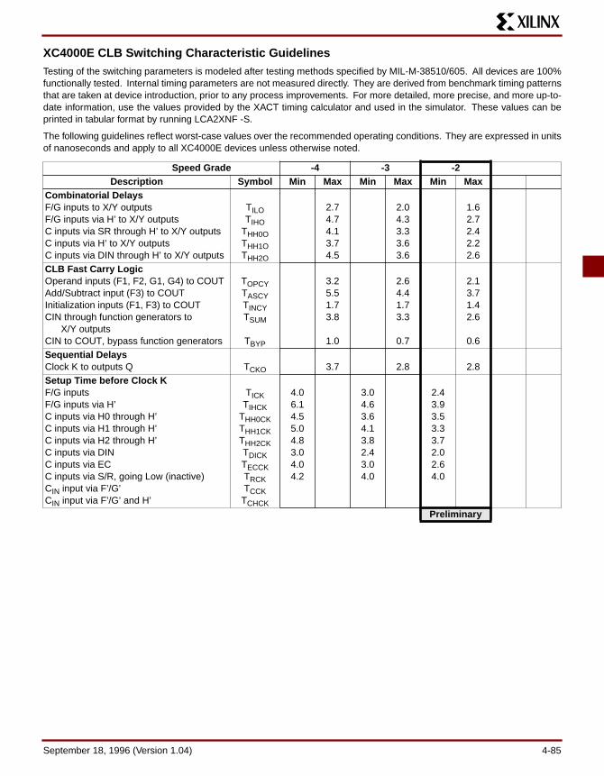
XC4000E CLB Switching Characteristic GuidelinesTesting of the switching parameters is modeled after testing methods specified by MIL-M-38510/605. All devices are 100%functionally tested. Internal timing parameters are not measured directly. They are derived from benchmark timing patternsthat are taken at device introduction, prior to any process improvements. For more detailed, more precise, and more up-to-date information, use the values provided by the XACT timing calculator and used in the simulator. These values can beprinted in tabular format by running LCA2XNF -S.
The following guidelines reflect worst-case values over the recommended operating conditions. They are expressed in unitsof nanoseconds and apply to all XC4000E devices unless otherwise noted.
Speed Grade -4 -3 -2Description Symbol Min Max Min Max Min Max
Combinatorial DelaysF/G inputs to X/Y outputsF/G inputs via H’ to X/Y outputsC inputs via SR through H’ to X/Y outputsC inputs via H’ to X/Y outputsC inputs via DIN through H’ to X/Y outputs
TILOTIHO
THH0OTHH1OTHH2O
2.74.74.13.74.5
2.04.33.33.63.6
1.62.72.42.22.6
CLB Fast Carry Logic Operand inputs (F1, F2, G1, G4) to COUTAdd/Subtract input (F3) to COUTInitialization inputs (F1, F3) to COUTCIN through function generators to X/Y outputsCIN to COUT, bypass function generators
TOPCYTASCYTINCYTSUM
TBYP
3.25.51.73.8
1.0
2.64.41.73.3
0.7
2.13.71.42.6
0.6Sequential DelaysClock K to outputs Q TCKO 3.7 2.8 2.8Setup Time before Clock KF/G inputsF/G inputs via H’C inputs via H0 through H’C inputs via H1 through H’C inputs via H2 through H’C inputs via DINC inputs via ECC inputs via S/R, going Low (inactive)CIN input via F’/G’CIN input via F’/G’ and H’
TICKTIHCK
THH0CKTHH1CKTHH2CKTDICKTECCKTRCKTCCK
TCHCK
4.06.14.55.04.83.04.04.2
3.04.63.64.13.82.43.04.0
2.43.93.53.33.72.02.64.0
Preliminary
September 18, 1996 (Version 1.04) 4-85

XC4000 Series Field Programmable Gate Arrays
XC4000E CLB Switching Characteristic Guidelines (continued)Testing of the switching parameters is modeled after testing methods specified by MIL-M-38510/605. All devices are 100%functionally tested. Internal timing parameters are not measured directly. They are derived from benchmark timing patternsthat are taken at device introduction, prior to any process improvements. For more detailed, more precise, and more up-to-date information, use the values provided by the XACT timing calculator and used in the simulator. These values can beprinted in tabular format by running LCA2XNF -S.
The following guidelines reflect worst-case values over the recommended operating conditions. They are expressed in unitsof nanoseconds and apply to all XC4000E devices unless otherwise noted.
Note 1: Timing is based on the XC4005E. For other devices see the XACT timing calculator.Note 2: Export Control Max. flip-flop toggle rate.
Speed Grade -4 -3 -2Description Symbol Min Max Min Max Min Max
Hold Time after Clock KF/G inputs F/G inputs via H’C inputs via H0 through H’C inputs via H1 through H’C inputs via H2 through H’C inputs via DINC inputs via ECC inputs via SR, going Low (inactive)
TCKITCKIH
TCKHH0TCKHH1TCKHH2TCKDITCKECTCKR
00000000
00000000
00000000
Clock Clock High timeClock Low time
TCHTCL
4.54.5
4.04.0
4.04.0
Set/Reset DirectWidth (High)Delay from C inputs via S/R, going High to Q
TRPWTRIO
5.56.5
4.04.0
4.04.0
Master Set/Reset (Note 1)Width (High or Low)Delay from Global Set/Reset net to QGlobal Set/Reset inactive to first active clock K edge
TMRWTMRQTMRK
13.023.0
11.518.7
11.517.4
Toggle Frequency2 (MHz) (Note 2) FTOG 113 142 160Preliminary
4-86 September 18, 1996 (Version 1.04)

XC4000E CLB Edge-Triggered (Synchronous) RAM Switching Characteristic GuidelinesTesting of the switching parameters is modeled after testing methods specified by MIL-M-38510/605. All devices are 100%functionally tested. Internal timing parameters are not measured directly. They are derived from benchmark timing patternsthat are taken at device introduction, prior to any process improvements. For more detailed, more precise, and more up-to-date information, use the values provided by the XACT timing calculator and used in the simulator. These values can beprinted in tabular format by running LCA2XNF -S.
The following guidelines reflect worst-case values over the recommended operating conditions. They are expressed in unitsof nanoseconds and apply to all XC4000E devices unless otherwise noted.
Note 1: Timing for the 16x1 RAM option is identical to 16x2 RAM timing.Note 2: Applicable Read timing specifications are identical to Level-Sensitive Read timing.
Speed Grade -4 -3 -2Description Size Symbol Min Max Min Max Min Max
Write OperationAddress write cycle time (clock K period) Clock K pulse width (active edge)Address setup time before clock K Address hold time after clock KDIN setup time before clock KDIN hold time after clock KWE setup time before clock KWE hold time after clock KData valid after clock K
16x232x116x232x116x232x116x232x116x232x116x232x116x232x116x232x116x232x1
TWCSTWCTSTWPSTWPTSTASSTASTSTAHSTAHTSTDSSTDSTSTDHSTDHTSTWSSTWSTSTWHSTWHTSTWOSTWOTS
15.015.07.57.52.82.800
3.52.500
2.22.200
1 ms1 ms
10.311.6
14.414.47.27.22.42.400
3.21.900
2.02.000
1 ms1 ms
8.810.3
11.611.65.85.82.02.000
2.71.700
1.61.600
1 ms1 ms
7.99.3
Preliminary
X6461
WCLK (K)
WE
ADDRESS
DATA IN
DATA OUT OLD NEW
TDSSTDHS
TASS TAHS
TWSS
TWPS
TWHS
TWOS
TILOTILO
September 18, 1996 (Version 1.04) 4-87

XC4000 Series Field Programmable Gate Arrays
XC4000E CLB Edge-Triggered (Synchronous) Dual-Port RAM Switching Characteristic GuidelinesTesting of the switching parameters is modeled after testing methods specified by MIL-M-38510/605. All devices are 100%functionally tested. Internal timing parameters are not measured directly. They are derived from benchmark timing patternsthat are taken at device introduction, prior to any process improvements. For more detailed, more precise, and more up-to-date information, use the values provided by the XACT timing calculator and used in the simulator. These values can beprinted in tabular format by running LCA2XNF -S.
The following guidelines reflect worst-case values over the recommended operating conditions. They are expressed in unitsof nanoseconds and apply to all XC4000E devices unless otherwise noted.
Note: Applicable Read timing specifications are identical to16x2 Level-Sensitive Read timing.
Speed Grade -4 -3 -2Description Size Symbol Min Max Min Max Min Max
Write OperationAddress write cycle time (clock K period) Clock K pulse width (active edge)Address setup time before clock K Address hold time after clock KDIN setup time before clock KDIN hold time after clock KWE setup time before clock KWE hold time after clock KData valid after clock K
16x1
16x116x116x116x116x116x116x116x1
TWCDS
TWPDSTASDSTAHDSTDSDSTDHDSTWSDSTWHDSTWODS
15.0
7.52.80
2.20
2.20.3
1 ms
10.0
14.4
7.22.50
1.90
2.00
1 ms
7.8
11.6
5.82.10
1.60
1.60
1 ms
7.0Preliminary
WCLK (K)
WE
ADDRESS
DATA IN
TDSDSTDHDS
TASDS TAHDS
TWSDS
TWPDS
TWHDS
X6474
DATA OUT OLD NEW
TWODS
TILOTILO
4-88 September 18, 1996 (Version 1.04)

XC4000E CLB Level-Sensitive RAM Switching Characteristic GuidelinesTesting of the switching parameters is modeled after testing methods specified by MIL-M-38510/605. All devices are 100%functionally tested. Internal timing parameters are not measured directly. They are derived from benchmark timing patternsthat are taken at device introduction, prior to any process improvements. For more detailed, more precise, and more up-to-date information, use the values provided by the XACT timing calculator and used in the simulator. These values can beprinted in tabular format by running LCA2XNF -S.
The following guidelines reflect worst-case values over the recommended operating conditions. They are expressed in unitsof nanoseconds and apply to all XC4000E devices unless otherwise noted.
Note: Timing for the 16x1 RAM option is identical to 16x2 RAM timing.
Speed Grade -4 -3 -2Description Size Symbol Min Max Min Max Min Max
Write OperationAddress write cycle time
Write Enable pulse width (High)Address setup time before WE Address hold time after end of WEDIN setup time before end of WEDIN hold time after end of WE
16x232x116x232x116x232x116x232x116x232x116x232x1
TWCTWCTTWPTWPTTASTASTTAHTAHTTDSTDSTTDHTDHT
8.08.04.04.02.02.02.52.04.05.02.02.0
8.08.04.04.02.02.02.02.02.22.22.02.0
8.08.04.04.02.02.02.02.00.80.82.02.0
Read Operation Address read cycle time
Data valid after address change (no Write Enable)
16x232x116x232x1
TRCTRCTTILOTIHO
4.56.5
2.74.7
3.15.5
2.04.3
2.63.8
1.62.7
Read Operation, Clocking Data into Flip-FlopAddress setup time before clock K
16x232x1
TICKTIHCK
4.06.1
3.04.6
2.43.9
Read During WriteData valid after WE goes active (DIN stable before WE)Data valid after DIN (DIN changes during WE)
16x232x1
16x232x1
TWOTWOT
TDOTDOT
10.012.0
9.011.0
6.07.3
6.67.6
4.95.6
5.86.2
Read During Write, Clock- ing Data into Flip-FlopWE setup time before clock KData setup time before clock K
16x232x116x232x1
TWCKTWCKTTDCKTDCKT
8.09.67.08.0
6.06.85.26.2
5.15.84.45.3Preliminary
September 18, 1996 (Version 1.04) 4-89

XC4000 Series Field Programmable Gate Arrays
XC4000E CLB Level-Sensitive RAM Timing Characteristics
WCT
ILOT
CKOT
DOT
DHT
WOT
CKOT
WCKT
DCKT
ICKT CH T
WOT
WPT
VALID
VALID (OLD)
VALID (OLD)
VALID (PREVIOUS)
VALID (NEW)
VALID (NEW)
VALID
ADDRESS
X,Y OUTPUTS
CLOCK
XQ, YQ OUTPUTS
WRITE ENABLE
X, Y OUTPUTS
X, Y OUTPUTS
XQ, YQ OUTPUTS
WRITE ENABLE
DATA IN
CLOCK
DATA IN (stable during WE)
DATA IN (changing during WE)
READ WITHOUT WRITE
READ, CLOCKING DATA INTO FLIP-FLOP
READ DURING WRITE, CLOCKING DATA INTO FLIP-FLOP
READ DURING WRITE
WRITE ENABLE
DATA IN
WRITEAST WPT
DST DHT
REQUIRED
AHT
WPT
OLD NEW
VALID VALID
X2640
4-90 September 18, 1996 (Version 1.04)
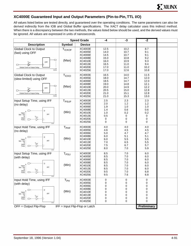
XC4000E Guaranteed Input and Output Parameters (Pin-to-Pin, TTL I/O)All values listed below are tested directly, and guaranteed over the operating conditions. The same parameters can also bederived indirectly from the IOB and Global Buffer specifications. The XACT delay calculator uses this indirect method.When there is a discrepancy between the two methods, the values listed below should be used, and the derived values mustbe ignored. All values are expressed in units of nanoseconds.
Speed Grade -4 -3 -2Description Symbol Device
Global Clock to Output (fast) using OFF
TICKOF
(Max)
XC4003EXC4005EXC4006EXC4008EXC4010EXC4013EXC4020EXC4025E
12.514.014.515.016.016.517.017.0
10.210.710.710.810.911.011.012.6
8.79.19.19.29.39.4
10.210.8
Global Clock to Output (slew-limited) using OFF
TICKO
(Max)
XC4003EXC4005EXC4006EXC4008EXC4010EXC4013EXC4020EXC4025E
16.518.018.519.020.020.521.021.0
14.014.714.714.814.915.015.115.3
11.512.012.012.112.212.812.813.0
Input Setup Time, using IFF (no delay)
TPSUF
(Min)
XC4003EXC4005EXC4006EXC4008EXC4010EXC4013EXC4020EXC4025E
2.52.01.91.41.00.500
2.31.21.00.60.2000
2.31.21.00.60.2000
Input Hold Time, using IFF (no delay)
TPHF
(Min)
XC4003EXC4005EXC4006EXC4008EXC4010EXC4013EXC4020EXC4025E
4.04.65.06.06.07.07.58.0
4.04.54.75.15.56.56.77.0
4.04.54.75.15.55.55.75.9
Input Setup Time, using IFF(with delay)
TPSU
(Min)
XC4003EXC4005EXC4006EXC4008EXC4010EXC4013EXC4020EXC4025E
8.58.58.58.58.58.59.59.5
7.07.07.07.07.07.07.07.6
6.06.06.06.06.06.06.86.8
Input Hold Time, using IFF(with delay)
TPH
(Min)
XC4003EXC4005EXC4006EXC4008EXC4010EXC4013EXC4020EXC4025E
00000000
00000000
00000000
OFF = Output Flip-Flop IFF = Input Flip-Flop or Latch Preliminary
OFF
Global Clock-to-Output Delay
.....X3202
TPG
OFF
Global Clock-to-Output Delay
.....X3202
TPG
IFF
D
X3201
Input Set - Up
& Hold Time
TPG
IFF
D
X3201
Input Set - Up
& Hold Time
TPG
IFF
D
X3201
Input Set - Up
& Hold Time
TPG
IFF
D
X3201
Input Set - Up
& Hold Time
TPG
September 18, 1996 (Version 1.04) 4-91
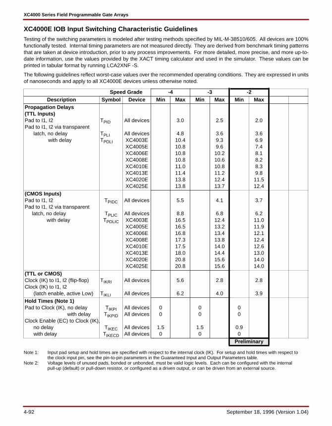
XC4000 Series Field Programmable Gate Arrays
XC4000E IOB Input Switching Characteristic GuidelinesTesting of the switching parameters is modeled after testing methods specified by MIL-M-38510/605. All devices are 100%functionally tested. Internal timing parameters are not measured directly. They are derived from benchmark timing patternsthat are taken at device introduction, prior to any process improvements. For more detailed, more precise, and more up-to-date information, use the values provided by the XACT timing calculator and used in the simulator. These values can beprinted in tabular format by running LCA2XNF -S.
The following guidelines reflect worst-case values over the recommended operating conditions. They are expressed in unitsof nanoseconds and apply to all XC4000E devices unless otherwise noted.
Note 1: Input pad setup and hold times are specified with respect to the internal clock (IK). For setup and hold times with respect to the clock input pin, see the pin-to-pin parameters in the Guaranteed Input and Output Parameters table.
Note 2: Voltage levels of unused pads, bonded or unbonded, must be valid logic levels. Each can be configured with the internal pull-up (default) or pull-down resistor, or configured as a driven output, or can be driven from an external source.
Speed Grade -4 -3 -2Description Symbol Device Min Max Min Max Min Max
Propagation Delays (TTL Inputs)Pad to I1, I2Pad to I1, I2 via transparent latch, no delay with delay
TPID
TPLITPDLI
All devices
All devicesXC4003EXC4005EXC4006EXC4008EXC4010EXC4013EXC4020EXC4025E
3.0
4.810.410.810.810.811.011.413.813.8
2.5
3.69.39.610.210.610.811.212.413.7
2.0
3.66.97.48.18.28.39.811.512.4
(CMOS Inputs)Pad to I1, I2Pad to I1, I2 via transparent latch, no delay with delay
TPIDC
TPLICTPDLIC
All devices
All devicesXC4003EXC4005EXC4006EXC4008EXC4010EXC4013EXC4020EXC4025E
5.5
8.816.516.516.817.317.518.020.820.8
4.1
6.812.413.213.413.814.014.415.615.6
3.7
6.211.011.912.112.412.613.014.014.0
(TTL or CMOS)Clock (IK) to I1, I2 (flip-flop)Clock (IK) to I1, I2 (latch enable, active Low)
TIKRI
TIKLI
All devices
All devices
5.6
6.2
2.8
4.0
2.8
3.9Hold Times (Note 1)Pad to Clock (IK), no delay with delayClock Enable (EC) to Clock (IK), no delay with delay
TIKPITIKPID
TIKECTIKECD
All devicesAll devices
All devicesAll devices
00
1.50
00
1.50
00
0.90
Preliminary
4-92 September 18, 1996 (Version 1.04)

XC4000E IOB Input Switching Characteristic Guidelines (continued)Testing of the switching parameters is modeled after testing methods specified by MIL-M-38510/605. All devices are 100%functionally tested. Internal timing parameters are not measured directly. They are derived from benchmark timing patternsthat are taken at device introduction, prior to any process improvements. For more detailed, more precise, and more up-to-date information, use the values provided by the XACT timing calculator and used in the simulator. These values can beprinted in tabular format by running LCA2XNF -S.
The following guidelines reflect worst-case values over the recommended operating conditions. They are expressed in unitsof nanoseconds and apply to all XC4000E devices unless otherwise noted.
Note 1: Input pad setup and hold times are specified with respect to the internal clock (IK). For setup and hold times with respect to the clock input pin, see the pin-to-pin parameters in the Guaranteed Input and Output Parameters table.
Note 2: Voltage levels of unused pads, bonded or unbonded, must be valid logic levels. Each can be configured with the internal pull-up (default) or pull-down resistor, or configured as a driven output, or can be driven from an external source.
Note 3: Timing is based on the XC4005E. For other devices see the XACT timing calculator.
Speed Grade -4 -3 -2Description Symbol Device Min Max Min Max Min Max
Setup Times (TTL Inputs)Pad to Clock (IK), no delay
with delayTPICK
TPICKD
All devicesXC4003EXC4005EXC4006EXC4008EXC4010EXC4013EXC4020EXC4025E
4.010.910.910.911.111.311.814.014.0
2.68.28.79.29.69.810.211.411.4
2.06.06.16.26.36.47.99.410.0
(CMOS Inputs) Pad to Clock (IK), no delay
with delayTPICKC
TPICKDC
All devicesXC4003EXC4005EXC4006EXC4008EXC4010EXC4013EXC4020EXC4025E
6.012.012.012.312.813.013.516.016.0
3.38.89.79.910.310.510.912.112.1
2.46.98.08.18.28.310.012.112.1
(TTL or CMOS)Clock Enable (EC) to Clock (IK), no delay
with delayTECIK
TECIKD
All devicesXC4003EXC4005EXC4006EXC4008EXC4010EXC4013EXC4020EXC4025E
3.510.410.410.410.410.711.114.014.0
2.58.18.59.19.59.710.111.311.3
2.14.35.66.76.97.19.010.611.0
Global Set/Reset (Note 3)Delay from GSR net through Q to I1, I2GSR widthGSR inactive to first active Clock (IK) edge
TRRI
TMRWTMRI
13.0
12.0
11.5
7.8
11.5
6.8
Preliminary
September 18, 1996 (Version 1.04) 4-93

XC4000 Series Field Programmable Gate Arrays
XC4000E IOB Output Switching Characteristic GuidelinesTesting of the switching parameters is modeled after testing methods specified by MIL-M-38510/605. All devices are 100%functionally tested. Internal timing parameters are not measured directly. They are derived from benchmark timing patternsthat are taken at device introduction, prior to any process improvements. For more detailed, more precise, and more up-to-date information, use the values provided by the XACT timing calculator and used in the simulator. These values can beprinted in tabular format by running LCA2XNF -S.
The following guidelines reflect worst-case values over the recommended operating conditions. They are expressed in unitsof nanoseconds and apply to all XC4000E devices unless otherwise noted.
Note 1: Output timing is measured at pin threshold, with 50pF external capacitive loads (incl. test fixture). Slew-rate limited output rise/fall times are approximately two times longer than fast output rise/fall times. For the effect of capacitive loads on ground bounce, see the “Additional XC4000 Data” section of the Programmable Logic Data Book.
Note 2: Voltage levels of unused pads, bonded or unbonded, must be valid logic levels. Each can be configured with the internal pull-up (default) or pull-down resistor, or configured as a driven output, or can be driven from an external source.
Speed Grade -4 -3 -2Description Symbol Min Max Min Max Min Max
Propagation Delays(TTL Output Levels)Clock (OK) to Pad, fast slew-rate limitedOutput (O) to Pad, fast slew-rate limited3-state to Pad hi-Z (slew-rate independent)3-state to Pad active and valid, fast slew-rate limited
TOKPOFTOKPOS
TOPFTOPSTTSHZ
TTSONFTTSONS
7.511.58.012.05.0
9.713.7
6.59.55.58.54.2
8.111.1
4.57.04.87.33.8
7.39.8
Propagation Delays(CMOS Output Levels)Clock (OK) to Pad, fast slew-rate limitedOutput (O) to Pad, fast slew-rate limited3-state to Pad hi-Z (slew-rate independent)3-state to Pad active and valid, fast slew-rate limited
TOKPOFCTOKPOSC
TOPFCTOPSCTTSHZC
TTSONFCTTSONSC
9.513.510.014.05.2
9.113.1
7.811.69.713.44.3
7.611.4
7.010.48.712.13.9
6.810.2
Preliminary
4-94 September 18, 1996 (Version 1.04)
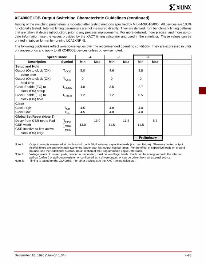
XC4000E IOB Output Switching Characteristic Guidelines (continued)Testing of the switching parameters is modeled after testing methods specified by MIL-M-38510/605. All devices are 100%functionally tested. Internal timing parameters are not measured directly. They are derived from benchmark timing patternsthat are taken at device introduction, prior to any process improvements. For more detailed, more precise, and more up-to-date information, use the values provided by the XACT timing calculator and used in the simulator. These values can beprinted in tabular format by running LCA2XNF -S.
The following guidelines reflect worst-case values over the recommended operating conditions. They are expressed in unitsof nanoseconds and apply to all XC4000E devices unless otherwise noted.
Note 1: Output timing is measured at pin threshold, with 50pF external capacitive loads (incl. test fixture). Slew-rate limited output rise/fall times are approximately two times longer than fast output rise/fall times. For the effect of capacitive loads on ground bounce, see the “Additional XC4000 Data” section of the Programmable Logic Data Book.
Note 2: Voltage levels of unused pads, bonded or unbonded, must be valid logic levels. Each can be configured with the internal pull-up (default) or pull-down resistor, or configured as a driven output, or can be driven from an external source.
Note 3: Timing is based on the XC4005E. For other devices see the XACT timing calculator.
Speed Grade -4 -3 -2Description Symbol Min Max Min Max Min Max
Setup and HoldOutput (O) to clock (OK) setup timeOutput (O) to clock (OK) hold timeClock Enable (EC) to clock (OK) setupClock Enable (EC) to clock (OK) hold
TOOK
TOKO
TECOK
TOKEC
5.0
0
4.8
1.2
4.6
0
3.5
1.2
3.8
0
2.7
0.5
ClockClock HighClock Low
TCHTCL
4.54.5
4.04.0
4.04.0
Global Set/Reset (Note 3)Delay from GSR net to PadGSR widthGSR inactive to first active clock (OK) edge
TRPOTMRWTMRO
13.015.0
11.511.8
11.58.7
Preliminary
September 18, 1996 (Version 1.04) 4-95

XC4000 Series Field Programmable Gate Arrays
XC4000E Boundary Scan (JTAG) Switching Characteristic GuidelinesTesting of the switching parameters is modeled after testing methods specified by MIL-M-38510/605. All devices are 100%functionally tested. Internal timing parameters are not measured directly. They are derived from benchmark timing patternsthat are taken at device introduction, prior to any process improvements. For more detailed, more precise, and more up-to-date information, use the values provided by the XACT timing calculator and used in the simulator. These values can beprinted in tabular format by running LCA2XNF -S.
The following guidelines reflect worst-case values over the recommended operating conditions. They are expressed in unitsof nanoseconds and apply to all XC4000E devices unless otherwise noted.
Note 1: Input pad setup and hold times are specified with respect to the internal clock (IK). For setup and hold times with respect to the clock input pin, see the pin-to-pin parameters in the Guaranteed Input and Output Parameters table.
Note 2: Output timing is measured at pin threshold, with 50pF external capacitive loads (incl. test fixture). Slew-rate limited output rise/fall times are approximately two times longer than fast output rise/fall times. For the effect of capacitive loads on ground bounce, see the “Additional XC4000 Data” section of the Programmable Logic Data Book.
Note 3: Voltage levels of unused pads, bonded or unbonded, must be valid logic levels. Each can be configured with the internal pull-up (default) or pull-down resistor, or configured as a driven output, or can be driven from an external source.
XC4000L Switching CharacteristicsXC4000L timing parameters were not available at the time this document was released. See the Xilinx WEBLINX at http://www.xilinx.com for the latest available information.
XC4000EX Switching CharacteristicsXC4000EX timing parameters were not available at the time this document was released. See the Xilinx WEBLINX at http://www.xilinx.com for the latest available information.
XC4000XL Switching CharacteristicsXC4000XL timing parameters were not available at the time this document was released. See the Xilinx WEBLINX at http://www.xilinx.com for the latest available information.
Speed Grade -4 -3 -2Description Symbol Min Max Min Max Min Max
Setup and HoldInput (TDI) to clock (TCK) setup timeInput (TDI) to clock (TCK) hold timeInput (TMS) to clock (TCK) setup timeInput (TMS) to clock (TCK) hold time
TTDITCK
TTCKTDI
TTMSTCK
TTCKTMS
Propagation DelayClock (TCK) to Pad (TDO) TTCKPO
ClockClock (TCK) HighClock (TCK) Low
TTCKHTTCKL
Power-On ResetJTAG operation after valid Vcc
TRJTAG
Preliminary
4-96 September 18, 1996 (Version 1.04)

Device-Specific Pinout Tables
Pin Locations for XC4003E DevicesThe following table may contain pinout information forunsupported device/package combinations. Please see theavailability charts elsewhere in the XC4000 Series datasheet for availability information.
4/2/96
Additional No Connect (N.C.) Connections on PG120 Package
2/28/96
XC4003EPad Name
PC84
PQ100
VQ100
PG120
BndryScan
VCC P2 P92 P89 G3 -I/O (A8) P3 P93 P90 G1 32I/O (A9) P4 P94 P91 F1 35I/O - P95 P92 E1 38I/O - P96 P93 F2 41I/O (A10) P5 P97 P94 F3 44I/O (A11) P6 P98 P95 D1 47I/O (A12) P7 P99 P96 C1 50I/O (A13) P8 P100 P97 D2 53I/O (A14) P9 P1 P98 C2 56I/O, SGCK1 (A15) P10 P2 P99 D3 59VCC P11 P3 P100 C3 -GND P12 P4 P1 C4 -I/O, PGCK1 (A16) P13 P5 P2 B2 62I/O (A17) P14 P6 P3 B3 65I/O, TDI P15 P7 P4 C5 68I/O, TCK P16 P8 P5 B4 71I/O, TMS P17 P9 P6 B5 74I/O P18 P10 P7 A4 77I/O - - - C6 80I/O - P11 P8 A5 83I/O P19 P12 P9 B6 86I/O P20 P13 P10 A6 89GND P21 P14 P11 B7 -VCC P22 P15 P12 C7 -I/O P23 P16 P13 A7 92I/O P24 P17 P14 A8 95I/O - P18 P15 A9 98I/O - - - B8 101I/O P25 P19 P16 C8 104I/O P26 P20 P17 A10 107I/O P27 P21 P18 B9 110I/O - P22 P19 A11 113I/O P28 P23 P20 C9 116I/O, SCGK2 P29 P24 P21 A12 119O (M1) P30 P25 P22 B11 122GND P31 P26 P23 C10 -I (M0) P32 P27 P24 C11 125VCC P33 P28 P25 D11 -I (M2) P34 P29 P26 B12 126I/O, PGCK2 P35 P30 P27 C12 127I/O (HDC) P36 P31 P28 A13 130I/O - P32 P29 D12 133I/O (LDC) P37 P33 P30 C13 136I/O P38 P34 P31 E12 139I/O P39 P35 P32 D13 142I/O - P36 P33 F11 145I/O - P37 P34 E13 148I/O P40 P38 P35 F12 151I/O (INIT) P41 P39 P36 F13 154VCC P42 P40 P37 G12 -GND P43 P41 P38 G11 -I/O P44 P42 P39 G13 157
I/O P45 P43 P40 H13 160I/O - P44 P41 J13 163I/O - P45 P42 H12 166I/O P46 P46 P43 H11 169I/O P47 P47 P44 K13 172I/O P48 P48 P45 J12 175I/O P49 P49 P46 L13 178I/O P50 P50 P47 M13 181I/O, SGCK3 P51 P51 P48 L12 184GND P52 P52 P49 K11 -DONE P53 P53 P50 L11 -VCC P54 P54 P51 L10 -PROGRAM P55 P55 P52 M12 -I/O (D7) P56 P56 P53 M11 187I/O, PGCK3 P57 P57 P54 N13 190I/O (D6) P58 P58 P55 M10 193I/O - P59 P56 N11 196I/O (D5) P59 P60 P57 M9 199I/O (CS0) P60 P61 P58 N10 202I/O - P62 P59 L8 205I/O - P63 P60 N9 208I/O (D4) P61 P64 P61 M8 211I/O P62 P65 P62 N8 214VCC P63 P66 P63 M7 -GND P64 P67 P64 L7 -I/O (D3) P65 P68 P65 N7 217I/O (RS) P66 P69 P66 N6 220I/O - P70 P67 N5 223I/O - - - M6 226I/O (D2) P67 P71 P68 L6 229I/O P68 P72 P69 N4 232I/O (D1) P69 P73 P70 M5 235I/O (RCLK, RDY/BUSY)
P70 P74 P71 N3 238
I/O (D0, DIN) P71 P75 P72 N2 241I/O, SGCK4 (DOUT)
P72 P76 P73 M3 244
CCLK P73 P77 P74 L4 -VCC P74 P78 P75 L3 -O, TDO P75 P79 P76 M2 0GND P76 P80 P77 K3 -I/O (A0, WS) P77 P81 P78 L2 2I/O, PGCK4 (A1) P78 P82 P79 N1 5I/O (CS1, A2) P79 P83 P80 K2 8I/O (A3) P80 P84 P81 L1 11I/O (A4) P81 P85 P82 J2 14I/O (A5) P82 P86 P83 K1 17I/O - P87 P84 H3 20I/O - P88 P85 J1 23I/O (A6) P83 P89 P86 H2 26I/O (A7) P84 P90 P87 H1 29GND P1 P91 P88 G2 -
PG120 PG120 PG120 PG120 PG120A1 B10 E11 L5 N12A2 B13 J3 L9A3 E2 J11 M1B1 E3 K12 M4
XC4003EPad Name
PC84
PQ100
VQ100
PG120
BndryScan
September 18, 1996 (Version 1.04) 4-97

XC4000 Series Field Programmable Gate Arrays
Pin Locations for XC4005E/L DevicesThe following table may contain pinout information forunsupported device/package combinations. Please see theavailability charts elsewhere in the XC4000 Series datasheet for availability information.
XC4005E/L
Pad Name
PC84
PQ100
TQ144
PG156
PQ160
PQ208
BndryScan
VCC P2 P92 P128 H3 P142 P183 -I/O (A8) P3 P93 P129 H1 P143 P184 44I/O (A9) P4 P94 P130 G1 P144 P185 47I/O - P95 P131 G2 P145 P186 50I/O - P96 P132 G3 P146 P187 53I/O (A10) P5 P97 P133 F1 P147 P190 56I/O (A11) P6 P98 P134 F2 P148 P191 59I/O - - P135 E1 P149 P192 62I/O - - P136 E2 P150 P193 65GND - - P137 F3 P151 P194 -I/O (A12) P7 P99 P138 E3 P154 P199 68I/O (A13) P8 P100 P139 C1 P155 P200 71I/O - - P140 C2 P156 P201 74I/O - - P141 D3 P157 P202 77I/O (A14) P9 P1 P142 B1 P158 P203 80I/O, SGCK1 (A15)
P10 P2 P143 B2 P159 P204 83
VCC P11 P3 P144 C3 P160 P205 -GND P12 P4 P1 C4 P1 P2 -I/O, PGCK1 (A16)
P13 P5 P2 B3 P2 P4 86
I/O (A17) P14 P6 P3 A1 P3 P5 89I/O - - P4 A2 P4 P6 92I/O - - P5 C5 P5 P7 95I/O, TDI P15 P7 P6 B4 P6 P8 98I/O, TCK P16 P8 P7 A3 P7 P9 101GND - - P8 C6 P10 P14 -I/O - - P9 B5 P11 P15 104I/O - - P10 B6 P12 P16 107I/O, TMS P17 P9 P11 A5 P13 P17 110I/O P18 P10 P12 C7 P14 P18 113I/O - - P13 B7 P15 P21 116I/O - P11 P14 A6 P16 P22 119I/O P19 P12 P15 A7 P17 P23 122I/O P20 P13 P16 A8 P18 P24 125GND P21 P14 P17 C8 P19 P25 -VCC P22 P15 P18 B8 P20 P26 -I/O P23 P16 P19 C9 P21 P27 128I/O P24 P17 P20 B9 P22 P28 131I/O - P18 P21 A9 P23 P29 134I/O - - P22 B10 P24 P30 137I/O P25 P19 P23 C10 P25 P33 140
I/O P26 P20 P24 A10 P26 P34 143I/O - - P25 A11 P27 P35 146I/O - - P26 B11 P28 P36 149GND - - P27 C11 P29 P37 -I/O P27 P21 P28 B12 P32 P42 152I/O - P22 P29 A13 P33 P43 155I/O - - P30 A14 P34 P44 158I/O - - P31 C12 P35 P45 161I/O P28 P23 P32 B13 P36 P46 164I/O,SCGK2
P29 P24 P33 B14 P37 P47 167
O (M1) P30 P25 P34 A15 P38 P48 170GND P31 P26 P35 C13 P39 P49 -I (M0) P32 P27 P36 A16 P40 P50 173VCC P33 P28 P37 C14 P41 P55 -I (M2) P34 P29 P38 B15 P42 P56 174I/O,PGCK2
P35 P30 P39 B16 P43 P57 175
I/O (HDC) P36 P31 P40 D14 P44 P58 178I/O - - P41 C15 P45 P59 181I/O - - P42 D15 P46 P60 184I/O - P32 P43 E14 P47 P61 187I/O (LDC) P37 P33 P44 C16 P48 P62 190GND - - P45 F14 P51 P67 -I/O - - P46 F15 P52 P68 193I/O - - P47 E16 P53 P69 196I/O P38 P34 P48 F16 P54 P70 199I/O P39 P35 P49 G14 P55 P71 202I/O - P36 P50 G15 P56 P74 205I/O - P37 P51 G16 P57 P75 208I/O P40 P38 P52 H16 P58 P76 211I/O (INIT) P41 P39 P53 H15 P59 P77 214VCC P42 P40 P54 H14 P60 P78 -GND P43 P41 P55 J14 P61 P79 -I/O P44 P42 P56 J15 P62 P80 217I/O P45 P43 P57 J16 P63 P81 220I/O - P44 P58 K16 P64 P82 223I/O - P45 P59 K15 P65 P83 226I/O P46 P46 P60 K14 P66 P86 229I/O P47 P47 P61 L16 P67 P87 232I/O - - P62 M16 P68 P88 235I/O - - P63 L15 P69 P89 238GND - - P64 L14 P70 P90 -I/O P48 P48 P65 P16 P73 P95 241I/O P49 P49 P66 M14 P74 P96 244I/O - - P67 N15 P75 P97 247I/O - - P68 P15 P76 P98 250I/O P50 P50 P69 N14 P77 P99 253
XC4005E/L
Pad Name
PC84
PQ100
TQ144
PG156
PQ160
PQ208
BndryScan
4-98 September 18, 1996 (Version 1.04)

4/2/96
Additional No Connect (N.C.) Connections on TQ144, PG156, PQ160 & PQ208 Packages
3/12/96
I/O, SGCK3
P51 P51 P70 R16 P78 P100 256
GND P52 P52 P71 P14 P79 P101 -DONE P53 P53 P72 R15 P80 P103 -VCC P54 P54 P73 P13 P81 P106 -PRO-GRAM
P55 P55 P74 R14 P82 P108 -
I/O (D7) P56 P56 P75 T16 P83 P109 259I/O, PGCK3
P57 P57 P76 T15 P84 P110 262
I/O - - P77 R13 P85 P111 265I/O - - P78 P12 P86 P112 268I/O (D6) P58 P58 P79 T14 P87 P113 271I/O - P59 P80 T13 P88 P114 274GND - - P81 P11 P91 P119 -I/O - - P82 R11 P92 P120 277I/O - - P83 T11 P93 P121 280I/O (D5) P59 P60 P84 T10 P94 P122 283I/O (CS0) P60 P61 P85 P10 P95 P123 286I/O - P62 P86 R10 P96 P126 289I/O - P63 P87 T9 P97 P127 292I/O (D4) P61 P64 P88 R9 P98 P128 295I/O P62 P65 P89 P9 P99 P129 298VCC P63 P66 P90 R8 P100 P130 -GND P64 P67 P91 P8 P101 P131 -I/O (D3) P65 P68 P92 T8 P102 P132 301I/O (RS) P66 P69 P93 T7 P103 P133 304I/O - P70 P94 T6 P104 P134 307I/O - - P95 R7 P105 P135 310I/O (D2) P67 P71 P96 P7 P106 P138 313I/O P68 P72 P97 T5 P107 P139 316I/O - - P98 R6 P108 P140 319I/O - - P99 T4 P109 P141 322GND - - P100 P6 P110 P142 -I/O (D1) P69 P73 P101 T3 P113 P147 325I/O (RCLK, RDY/BUSY)
P70 P74 P102 P5 P114 P148 328
I/O - - P103 R4 P115 P149 331I/O - - P104 R3 P116 P150 334I/O (D0, DIN)
P71 P75 P105 P4 P117 P151 337
I/O, SGCK4 (DOUT)
P72 P76 P106 T2 P118 P152 340
CCLK P73 P77 P107 R2 P119 P153 -VCC P74 P78 P108 P3 P120 P154 -O, TDO P75 P79 P109 T1 P121 P159 0GND P76 P80 P110 N3 P122 P160 -
XC4005E/L
Pad Name
PC84
PQ100
TQ144
PG156
PQ160
PQ208
BndryScan
I/O (A0, WS)
P77 P81 P111 R1 P123 P161 2
I/O, PGCK4 (A1)
P78 P82 P112 P2 P124 P162 5
I/O - - P113 N2 P125 P163 8I/O - - P114 M3 P126 P164 11I/O (CS1, A2)
P79 P83 P115 P1 P127 P165 14
I/O (A3) P80 P84 P116 N1 P128 P166 17GND - - P118 L3 P131 P171 -I/O - - P119 L2 P132 P172 20I/O - - P120 L1 P133 P173 23I/O (A4) P81 P85 P121 K3 P134 P174 26I/O (A5) P82 P86 P122 K2 P135 P175 29I/O - P87 P123 K1 P137 P178 32I/O - P88 P124 J1 P138 P179 35I/O (A6) P83 P89 P125 J2 P139 P180 38I/O (A7) P84 P90 P126 J3 P140 P181 41GND P1 P91 P127 H2 P141 P182 -
TQ144 PG156 PQ160 PQ208P117 A4 P8 P1
A12 P9 P3D1 P30 P10-P13D2 P31 P19-P20D16 P49 P31-P32E15 P50 P38-P41M1 P71 P51-P54M2 P72 P63-P66M15 P89 P72-P73N16 P90 P84-P85R5 P111 P91-P94R12 P112 P102T12 P129 P104-P105
P130 P107P136 P115-P118P152 P124-P125P153 P136-P137
P143-P146P155-P158P167-P170P176-P177P188-P189P195-P198P206-P208
XC4005E/L
Pad Name
PC84
PQ100
TQ144
PG156
PQ160
PQ208
BndryScan
September 18, 1996 (Version 1.04) 4-99

XC4000 Series Field Programmable Gate Arrays
Pin Locations for XC4006E DevicesThe following table may contain pinout information forunsupported device/package combinations. Please see theavailability charts elsewhere in the XC4000 Series datasheet for availability information.
XC4006EPad Name
PC84
TQ144
PG156
PQ160
PQ208
BndryScan
VCC P2 P128 H3 P142 P183 -
I/O (A8) P3 P129 H1 P143 P184 50
I/O (A9) P4 P130 G1 P144 P185 53
I/O - P131 G2 P145 P186 56
I/O - P132 G3 P146 P187 59
I/O (A10) P5 P133 F1 P147 P190 62
I/O (A11) P6 P134 F2 P148 P191 65
I/O - P135 E1 P149 P192 68
I/O - P136 E2 P150 P193 71
GND - P137 F3 P151 P194 -
I/O - - D1 P152 P197 74
I/O - - D2 P153 P198 77
I/O (A12) P7 P138 E3 P154 P199 80
I/O (A13) P8 P139 C1 P155 P200 83
I/O - P140 C2 P156 P201 86
I/O - P141 D3 P157 P202 89
I/O (A14) P9 P142 B1 P158 P203 92
I/O, SGCK1 (A15) P10 P143 B2 P159 P204 95
VCC P11 P144 C3 P160 P205 -
GND P12 P1 C4 P1 P2 -
I/O, PGCK1 (A16) P13 P2 B3 P2 P4 98
I/O (A17) P14 P3 A1 P3 P5 101
I/O - P4 A2 P4 P6 104
I/O - P5 C5 P5 P7 107
I/O, TDI P15 P6 B4 P6 P8 110
I/O, TCK P16 P7 A3 P7 P9 113
I/O - - A4 P8 P10 116
I/O - - - P9 P11 119
GND - P8 C6 P10 P14 -
I/O - P9 B5 P11 P15 122
I/O - P10 B6 P12 P16 125
I/O, TMS P17 P11 A5 P13 P17 128
I/O P18 P12 C7 P14 P18 131
I/O - P13 B7 P15 P21 134
I/O - P14 A6 P16 P22 137
I/O P19 P15 A7 P17 P23 140
I/O P20 P16 A8 P18 P24 143
GND P21 P17 C8 P19 P25 -
VCC P22 P18 B8 P20 P26 -
I/O P23 P19 C9 P21 P27 146
I/O P24 P20 B9 P22 P28 149
I/O - P21 A9 P23 P29 152
I/O - P22 B10 P24 P30 155
I/O P25 P23 C10 P25 P33 158
I/O P26 P24 A10 P26 P34 161
I/O - P25 A11 P27 P35 164
I/O - P26 B11 P28 P36 167
GND - P27 C11 P29 P37 -
I/O - - A12 P30 P40 170
I/O - - - P31 P41 173
I/O P27 P28 B12 P32 P42 176
I/O - P29 A13 P33 P43 179
I/O - P30 A14 P34 P44 182
I/O - P31 C12 P35 P45 185
I/O P28 P32 B13 P36 P46 188
I/O, SCGK2 P29 P33 B14 P37 P47 191
O (M1) P30 P34 A15 P38 P48 194
GND P31 P35 C13 P39 P49 -
I (M0) P32 P36 A16 P40 P50 197
VCC P33 P37 C14 P41 P55 -
I (M2) P34 P38 B15 P42 P56 198
I/O, PGCK2 P35 P39 B16 P43 P57 199
I/O (HDC) P36 P40 D14 P44 P58 202
I/O - P41 C15 P45 P59 205
I/O - P42 D15 P46 P60 208
I/O - P43 E14 P47 P61 211
I/O (LDC) P37 P44 C16 P48 P62 214
I/O - - E15 P49 P63 217
I/O - - D16 P50 P64 220
GND - P45 F14 P51 P67 -
I/O - P46 F15 P52 P68 223
I/O - P47 E16 P53 P69 226
I/O P38 P48 F16 P54 P70 229
I/O P39 P49 G14 P55 P71 232
I/O - P50 G15 P56 P74 235
I/O - P51 G16 P57 P75 238
I/O P40 P52 H16 P58 P76 241
I/O (INIT) P41 P53 H15 P59 P77 244
VCC P42 P54 H14 P60 P78 -
GND P43 P55 J14 P61 P79 -
I/O P44 P56 J15 P62 P80 247
I/O P45 P57 J16 P63 P81 250
I/O - P58 K16 P64 P82 253
I/O - P59 K15 P65 P83 256
I/O P46 P60 K14 P66 P86 259
I/O P47 P61 L16 P67 P87 262
I/O - P62 M16 P68 P88 265
I/O - P63 L15 P69 P89 268
GND - P64 L14 P70 P90 -
I/O - - N16 P71 P93 271
I/O - - M15 P72 P94 274
I/O P48 P65 P16 P73 P95 277
I/O P49 P66 M14 P74 P96 280
I/O - P67 N15 P75 P97 283
I/O - P68 P15 P76 P98 286
I/O P50 P69 N14 P77 P99 289
I/O, SGCK3 P51 P70 R16 P78 P100 292
XC4006EPad Name
PC84
TQ144
PG156
PQ160
PQ208
BndryScan
4-100 September 18, 1996 (Version 1.04)

4/2/96
Additional No Connect (N.C.) Connections on PQ160 & PQ208 Packages
2/28/96
GND P52 P71 P14 P79 P101 -
DONE P53 P72 R15 P80 P103 -
VCC P54 P73 P13 P81 P106 -
PROGRAM P55 P74 R14 P82 P108 -
I/O (D7) P56 P75 T16 P83 P109 295
I/O, PGCK3 P57 P76 T15 P84 P110 298
I/O - P77 R13 P85 P111 301
I/O - P78 P12 P86 P112 304
I/O (D6) P58 P79 T14 P87 P113 307
I/O - P80 T13 P88 P114 310
I/O - - R12 P89 P115 313
I/O - - T12 P90 P116 316
GND - P81 P11 P91 P119 -
I/O - P82 R11 P92 P120 319
I/O - P83 T11 P93 P121 322
I/O (D5) P59 P84 T10 P94 P122 325
I/O (CS0) P60 P85 P10 P95 P123 328
I/O - P86 R10 P96 P126 331
I/O - P87 T9 P97 P127 334
I/O (D4) P61 P88 R9 P98 P128 337
I/O P62 P89 P9 P99 P129 340
VCC P63 P90 R8 P100 P130 -
GND P64 P91 P8 P101 P131 -
I/O (D3) P65 P92 T8 P102 P132 343
I/O (RS) P66 P93 T7 P103 P133 346
I/O - P94 T6 P104 P134 349
I/O - P95 R7 P105 P135 352
I/O (D2) P67 P96 P7 P106 P138 355
I/O P68 P97 T5 P107 P139 358
I/O - P98 R6 P108 P140 361
I/O - P99 T4 P109 P141 364
GND - P100 P6 P110 P142 -
I/O - - R5 P111 P145 367
I/O - - - P112 P146 370
I/O (D1) P69 P101 T3 P113 P147 373
I/O (RCLK, RDY/BUSY)
P70 P102 P5 P114 P148 376
I/O - P103 R4 P115 P149 379
I/O - P104 R3 P116 P150 382
I/O (D0, DIN) P71 P105 P4 P117 P151 385
I/O, SGCK4 (DOUT)
P72 P106 T2 P118 P152 388
CCLK P73 P107 R2 P119 P153 -
VCC P74 P108 P3 P120 P154 -
O, TDO P75 P109 T1 P121 P159 0
GND P76 P110 N3 P122 P160 -
I/O (A0, WS) P77 P111 R1 P123 P161 2
I/O, PGCK4 (A1) P78 P112 P2 P124 P162 5
I/O - P113 N2 P125 P163 8
XC4006EPad Name
PC84
TQ144
PG156
PQ160
PQ208
BndryScan
I/O - P114 M3 P126 P164 11
I/O (CS1, A2) P79 P115 P1 P127 P165 14
I/O (A3) P80 P116 N1 P128 P166 17
I/O - P117 M2 P129 P167 20
I/O - - M1 P130 P168 23
GND - P118 L3 P131 P171 -
I/O - P119 L2 P132 P172 26
I/O - P120 L1 P133 P173 29
I/O (A4) P81 P121 K3 P134 P174 32
I/O (A5) P82 P122 K2 P135 P175 35
I/O - P123 K1 P137 P178 38
I/O - P124 J1 P138 P179 41
I/O (A6) P83 P125 J2 P139 P180 44
I/O (A7) P84 P126 J3 P140 P181 47
GND P1 P127 H2 P141 P182 -
PQ160 PQ208P136 P1
P3
P12-P13
P19-20
P31-P32
P38-P39
P51-P54
P65-P66
P72-P73
P84-P85
P91-P92
P102
P104-P105
P107
P117-P118
P124-P125
P136-P137
P143-P144
P155-P158
P169-P170
P176-P177
P188-P189
P195-P196
P206-P208
XC4006EPad Name
PC84
TQ144
PG156
PQ160
PQ208
BndryScan
September 18, 1996 (Version 1.04) 4-101

XC4000 Series Field Programmable Gate Arrays
Pin Locations for XC4008E DevicesThe following table may contain pinout information forunsupported device/package combinations. Please see theavailability charts elsewhere in the XC4000 Series datasheet for availability information.
XC4008E Pad Name PC84
PQ160
PG191
PQ208
BndryScan
VCC P2 P142 J4 P183 -
I/O (A8) P3 P143 J3 P184 56
I/O (A9) P4 P144 J2 P185 59
I/O - P145 J1 P186 62
I/O - P146 H1 P187 65
I/O - - H2 P188 68
I/O - - H3 P189 71
I/O (A10) P5 P147 G1 P190 74
I/O (A11) P6 P148 G2 P191 77
I/O - P149 F1 P192 80
I/O - P150 E1 P193 83
GND - P151 G3 P194 -
I/O - P152 C1 P197 86
I/O - P153 E2 P198 89
I/O (A12) P7 P154 F3 P199 92
I/O (A13) P8 P155 D2 P200 95
I/O - P156 B1 P201 98
I/O - P157 E3 P202 101
I/O (A14) P9 P158 C2 P203 104
I/O, SGCK1 (A15) P10 P159 B2 P204 107
VCC P11 P160 D3 P205 -
GND P12 P1 D4 P2 -
I/O, PGCK1 (A16) P13 P2 C3 P4 110
I/O (A17) P14 P3 C4 P5 113
I/O - P4 B3 P6 116
I/O - P5 C5 P7 119
I/O, TDI P15 P6 A2 P8 122
I/O, TCK P16 P7 B4 P9 125
I/O - P8 C6 P10 128
I/O - P9 A3 P11 131
GND - P10 C7 P14 -
I/O - P11 A4 P15 134
I/O - P12 A5 P16 137
I/O, TMS P17 P13 B7 P17 140
I/O P18 P14 A6 P18 143
I/O - - C8 P19 146
I/O - - A7 P20 149
I/O - P15 B8 P21 152
I/O - P16 A8 P22 155
I/O P19 P17 B9 P23 158
I/O P20 P18 C9 P24 161
GND P21 P19 D9 P25 -
VCC P22 P20 D10 P26 -
I/O P23 P21 C10 P27 164
I/O P24 P22 B10 P28 167
I/O - P23 A9 P29 170
I/O - P24 A10 P30 173
I/O - - A11 P31 176
I/O - - C11 P32 179
I/O P25 P25 B11 P33 182
I/O P26 P26 A12 P34 185
I/O - P27 B12 P35 188
I/O - P28 A13 P36 191
GND - P29 C12 P37 -
I/O - P30 A15 P40 194
I/O - P31 C13 P41 197
I/O P27 P32 B14 P42 200
I/O - P33 A16 P43 203
I/O - P34 B15 P44 206
I/O - P35 C14 P45 209
I/O P28 P36 A17 P46 212
I/O, SCGK2 P29 P37 B16 P47 215
O (M1) P30 P38 C15 P48 218
GND P31 P39 D15 P49 -
I (M0) P32 P40 A18 P50 221
VCC P33 P41 D16 P55 -
I (M2) P34 P42 C16 P56 222
I/O, PGCK2 P35 P43 B17 P57 223
I/O (HDC) P36 P44 E16 P58 226
I/O - P45 C17 P59 229
I/O - P46 D17 P60 232
I/O - P47 B18 P61 235
I/O (LDC) P37 P48 E17 P62 238
I/O - P49 F16 P63 241
I/O - P50 C18 P64 244
GND - P51 G16 P67 -
I/O - P52 E18 P68 247
I/O - P53 F18 P69 250
I/O P38 P54 G17 P70 253
I/O P39 P55 G18 P71 256
I/O - - H16 P72 259
I/O - - H17 P73 262
I/O - P56 H18 P74 265
I/O - P57 J18 P75 268
I/O P40 P58 J17 P76 271
I/O (INIT) P41 P59 J16 P77 274
VCC P42 P60 J15 P78 -
GND P43 P61 K15 P79 -
I/O P44 P62 K16 P80 277
I/O P45 P63 K17 P81 280
I/O - P64 K18 P82 283
I/O - P65 L18 P83 286
I/O - - L17 P84 289
I/O - - L16 P85 292
I/O P46 P66 M18 P86 295
I/O P47 P67 M17 P87 298
I/O - P68 N18 P88 301
I/O - P69 P18 P89 304
XC4008E Pad Name PC84
PQ160
PG191
PQ208
BndryScan
4-102 September 18, 1996 (Version 1.04)

4/2/96
Additional No Connect (N.C.) Connections on PG191 & PQ208 Packages
2/28/96
GND - P70 M16 P90 -
I/O - P71 T18 P93 307
I/O - P72 P17 P94 310
I/O P48 P73 N16 P95 313
I/O P49 P74 T17 P96 316
I/O - P75 R17 P97 319
I/O - P76 P16 P98 322
I/O P50 P77 U18 P99 325
I/O, SGCK3 P51 P78 T16 P100 328
GND P52 P79 R16 P101 -
DONE P53 P80 U17 P103 -
VCC P54 P81 R15 P106 -
PROGRAM P55 P82 V18 P108 -
I/O (D7) P56 P83 T15 P109 331
I/O, PGCK3 P57 P84 U16 P110 334
I/O - P85 T14 P111 337
I/O - P86 U15 P112 340
I/O (D6) P58 P87 V17 P113 343
I/O - P88 V16 P114 346
I/O - P89 T13 P115 349
I/O - P90 U14 P116 352
GND - P91 T12 P119 -
I/O - P92 U13 P120 355
I/O - P93 V13 P121 358
I/O (D5) P59 P94 U12 P122 361
I/O (CS0) P60 P95 V12 P123 364
I/O - - T11 P124 367
I/O - - U11 P125 370
I/O - P96 V11 P126 373
I/O - P97 V10 P127 376
I/O (D4) P61 P98 U10 P128 379
I/O P62 P99 T10 P129 382
VCC P63 P100 R10 P130 -
GND P64 P101 R9 P131 -
I/O (D3) P65 P102 T9 P132 385
I/O (RS) P66 P103 U9 P133 388
I/O - P104 V9 P134 391
I/O - P105 V8 P135 394
I/O - - U8 P136 397
I/O - - T8 P137 400
I/O (D2) P67 P106 V7 P138 403
I/O P68 P107 U7 P139 406
I/O - P108 V6 P140 409
I/O - P109 U6 P141 412
GND - P110 T7 P142 -
I/O - P111 U5 P145 415
I/O - P112 T6 P146 418
I/O (D1) P69 P113 V3 P147 421
I/O (RCLK, RDY/BUSY)
P70 P114 V2 P148 424
I/O - P115 U4 P149 427
I/O - P116 T5 P150 430
XC4008E Pad Name PC84
PQ160
PG191
PQ208
BndryScan
I/O (D0, DIN) P71 P117 U3 P151 433
I/O, SGCK4 (DOUT) P72 P118 T4 P152 436
CCLK P73 P119 V1 P153 -
VCC P74 P120 R4 P154 -
O, TDO P75 P121 U2 P159 0
GND P76 P122 R3 P160 -
I/O (A0, WS) P77 P123 T3 P161 2
I/O, PGCK4 (A1) P78 P124 U1 P162 5
I/O - P125 P3 P163 8
I/O - P126 R2 P164 11
I/O (CS1, A2) P79 P127 T2 P165 14
I/O (A3) P80 P128 N3 P166 17
I/O - P129 P2 P167 20
I/O - P130 T1 P168 23
GND - P131 M3 P171 -
I/O - P132 P1 P172 26
I/O - P133 N1 P173 29
I/O (A4) P81 P134 M2 P174 32
I/O (A5) P82 P135 M1 P175 35
I/O - - L3 P176 38
I/O - P136 L2 P177 41
I/O - P137 L1 P178 44
I/O - P138 K1 P179 47
I/O (A6) P83 P139 K2 P180 50
I/O (A7) P84 P140 K3 P181 53
GND P1 P141 K4 P182 -
PG191 PQ208 PQ208
A14 P1 P107
B5 P3 P117
B6 P12 P118
B13 P13 P143
D1 P38 P144
D18 P39 P155
F2 P51 P156
F17 P52 P157
N2 P53 P158
N17 P54 P169
R1 P65 P170
R18 P66 P195
V4 P91 P196
V5 P92 P206
V14 P102 P207
V15 P104 P208
P105
XC4008E Pad Name PC84
PQ160
PG191
PQ208
BndryScan
September 18, 1996 (Version 1.04) 4-103

XC4000 Series Field Programmable Gate Arrays
Pin Locations for XC4010E/L DevicesThe following table may contain pinout information forunsupported device/package combinations. Please see theavailability charts elsewhere in the XC4000 Series datasheet for availability information.
XC4010E/LPad Name
PC84
PQ160
TQ176
PG191
PQ/HQ208
BG225
Bndry Scan
VCC P2 P142 P155 J4 P183 D8 -I/O (A8) P3 P143 P156 J3 P184 E8 62I/O (A9) P4 P144 P157 J2 P185 B7 65I/O - P145 P158 J1 P186 A7 68I/O - P146 P159 H1 P187 C7 71I/O - - P160 H2 P188 D7 74I/O - - P161 H3 P189 E7 77I/O (A10) P5 P147 P162 G1 P190 A6 80I/O (A11) P6 P148 P163 G2 P191 B6 83I/O - P149 P164 F1 P192 A5 86I/O - P150 P165 E1 P193 B5 89GND - P151 P166 G3 P194 GND* -I/O - - - F2 P195 D6 92I/O - - P167 D1 P196 C5 95I/O - P152 P168 C1 P197 A4 98I/O - P153 P169 E2 P198 E6 101I/O (A12) P7 P154 P170 F3 P199 B4 104I/O (A13) P8 P155 P171 D2 P200 D5 107I/O - P156 P172 B1 P201 B3 110I/O - P157 P173 E3 P202 F6 113I/O (A14) P9 P158 P174 C2 P203 A2 116I/O, SGCK1 (A15)
P10 P159 P175 B2 P204 C3 119
VCC P11 P160 P176 D3 P205 B2 -GND P12 P1 P1 D4 P2 A1 -I/O, PGCK1 (A16)
P13 P2 P2 C3 P4 D4 122
I/O (A17) P14 P3 P3 C4 P5 B1 125I/O - P4 P4 B3 P6 C2 128I/O - P5 P5 C5 P7 E5 131I/O, TDI P15 P6 P6 A2 P8 D3 134I/O, TCK P16 P7 P7 B4 P9 C1 137I/O - P8 P8 C6 P10 D2 140I/O - P9 P9 A3 P11 G6 143I/O - - - B5 P12 E4 146I/O - - - B6 P13 D1 149GND - P10 P10 C7 P14 GND* -I/O - P11 P11 A4 P15 F5 152I/O - P12 P12 A5 P16 E1 155I/O, TMS P17 P13 P13 B7 P17 F4 158I/O P18 P14 P14 A6 P18 F3 161
I/O - - P15 C8 P19 G4 164I/O - - P16 A7 P20 G3 167I/O - P15 P17 B8 P21 G2 170I/O - P16 P18 A8 P22 G1 173I/O P19 P17 P19 B9 P23 G5 176I/O P20 P18 P20 C9 P24 H3 179GND P21 P19 P21 D9 P25 H2 -VCC P22 P20 P22 D10 P26 H1 -I/O P23 P21 P23 C10 P27 H4 182I/O P24 P22 P24 B10 P28 H5 185I/O - P23 P25 A9 P29 J2 188I/O - P24 P26 A10 P30 J1 191I/O - - P27 A11 P31 J3 194I/O - - P28 C11 P32 J4 197I/O P25 P25 P29 B11 P33 K2 200I/O P26 P26 P30 A12 P34 K3 203I/O - P27 P31 B12 P35 J6 206I/O - P28 P32 A13 P36 L1 209GND - P29 P33 C12 P37 GND* -I/O - - - B13 P38 L3 212I/O - - - A14 P39 M1 215I/O - P30 P34 A15 P40 K5 218I/O - P31 P35 C13 P41 M2 221I/O P27 P32 P36 B14 P42 L4 224I/O - P33 P37 A16 P43 N1 227I/O - P34 P38 B15 P44 M3 230I/O - P35 P39 C14 P45 N2 233I/O P28 P36 P40 A17 P46 K6 236I/O, SCGK2 P29 P37 P41 B16 P47 P1 239O (M1) P30 P38 P42 C15 P48 N3 242GND P31 P39 P43 D15 P49 GND* -I (M0) P32 P40 P44 A18 P50 P2 245VCC P33 P41 P45 D16 P55 R1 -I (M2) P34 P42 P46 C16 P56 M4 246I/O, PGCK2 P35 P43 P47 B17 P57 R2 247I/O (HDC) P36 P44 P48 E16 P58 P3 250I/O - P45 P49 C17 P59 L5 253I/O - P46 P50 D17 P60 N4 256I/O - P47 P51 B18 P61 R3 259I/O (LDC) P37 P48 P52 E17 P62 P4 262I/O - P49 P53 F16 P63 K7 265I/O - P50 P54 C18 P64 M5 268I/O - - - D18 P65 R4 271I/O - - - F17 P66 N5 274GND - P51 P55 G16 P67 GND* -I/O - P52 P56 E18 P68 R5 277
XC4010E/LPad Name
PC84
PQ160
TQ176
PG191
PQ/HQ208
BG225
Bndry Scan
4-104 September 18, 1996 (Version 1.04)

I/O - P53 P57 F18 P69 M6 280I/O P38 P54 P58 G17 P70 N6 283I/O P39 P55 P59 G18 P71 P6 286I/O - - P60 H16 P72 R6 289I/O - - P61 H17 P73 M7 292I/O - P56 P62 H18 P74 R7 295I/O - P57 P63 J18 P75 L7 298I/O P40 P58 P64 J17 P76 N8 301I/O (INIT) P41 P59 P65 J16 P77 P8 304VCC P42 P60 P66 J15 P78 R8 -GND P43 P61 P67 K15 P79 M8 -I/O P44 P62 P68 K16 P80 L8 307I/O P45 P63 P69 K17 P81 P9 310I/O - P64 P70 K18 P82 R9 313I/O - P65 P71 L18 P83 N9 316I/O - - P72 L17 P84 M9 319I/O - - P73 L16 P85 L9 322I/O P46 P66 P74 M18 P86 N10 325I/O P47 P67 P75 M17 P87 K9 328I/O - P68 P76 N18 P88 R11 331I/O - P69 P77 P18 P89 P11 334GND - P70 P78 M16 P90 GND* -I/O - - - N17 P91 R12 337I/O - - - R18 P92 L10 340I/O - P71 P79 T18 P93 P12 343I/O - P72 P80 P17 P94 M11 346I/O P48 P73 P81 N16 P95 R13 349I/O P49 P74 P82 T17 P96 N12 352I/O - P75 P83 R17 P97 P13 355I/O - P76 P84 P16 P98 K10 358I/O P50 P77 P85 U18 P99 R14 361I/O, SGCK3 P51 P78 P86 T16 P100 N13 364GND P52 P79 P87 R16 P101 GND* -DONE P53 P80 P88 U17 P103 P14 -VCC P54 P81 P89 R15 P106 R15 -PROGRAM P55 P82 P90 V18 P108 M12 -I/O (D7) P56 P83 P91 T15 P109 P15 367I/O, PGCK3 P57 P84 P92 U16 P110 N14 370I/O - P85 P93 T14 P111 L11 373I/O - P86 P94 U15 P112 M13 376I/O (D6) P58 P87 P95 V17 P113 J10 379I/O - P88 P96 V16 P114 L12 382I/O - P89 P97 T13 P115 M15 385I/O - P90 P98 U14 P116 L13 388I/O - - - V15 P117 L14 391I/O - - - V14 P118 K11 394
XC4010E/LPad Name
PC84
PQ160
TQ176
PG191
PQ/HQ208
BG225
Bndry Scan
GND - P91 P99 T12 P119 GND* -I/O - P92 P100 U13 P120 K13 397I/O - P93 P101 V13 P121 K14 400I/O (D5) P59 P94 P102 U12 P122 K15 403I/O (CS0) P60 P95 P103 V12 P123 J12 406I/O - - P104 T11 P124 J13 409I/O - - P105 U11 P125 J14 412I/O - P96 P106 V11 P126 J15 415I/O - P97 P107 V10 P127 J11 418I/O (D4) P61 P98 P108 U10 P128 H13 421I/O P62 P99 P109 T10 P129 H14 424VCC P63 P100 P110 R10 P130 H15 -GND P64 P101 P111 R9 P131 GND* -I/O (D3) P65 P102 P112 T9 P132 H12 427I/O (RS) P66 P103 P113 U9 P133 H11 430I/O - P104 P114 V9 P134 G14 433I/O - P105 P115 V8 P135 G15 436I/O - - P116 U8 P136 G13 439I/O - - P117 T8 P137 G12 442I/O (D2) P67 P106 P118 V7 P138 G11 445I/O P68 P107 P119 U7 P139 F15 448I/O - P108 P120 V6 P140 F14 451I/O - P109 P121 U6 P141 F13 454GND - P110 P122 T7 P142 GND* -I/O - - - V5 P143 E13 457I/O - - - V4 P144 D15 460I/O - P111 P123 U5 P145 F11 463I/O - P112 P124 T6 P146 D14 466I/O (D1) P69 P113 P125 V3 P147 E12 469I/O (RCLK, RDY/BUSY)
P70 P114 P126 V2 P148 C15 472
I/O - P115 P127 U4 P149 D13 475I/O - P116 P128 T5 P150 C14 478I/O (D0, DIN)
P71 P117 P129 U3 P151 F10 481
I/O, SGCK4 (DOUT)
P72 P118 P130 T4 P152 B15 484
CCLK P73 P119 P131 V1 P153 C13 -VCC P74 P120 P132 R4 P154 B14 -O, TDO P75 P121 P133 U2 P159 A15 0GND P76 P122 P134 R3 P160 D12 -I/O (A0, WS)
P77 P123 P135 T3 P161 A14 2
I/O, PGCK4 (A1)
P78 P124 P136 U1 P162 B13 5
I/O - P125 P137 P3 P163 E11 8
XC4010E/LPad Name
PC84
PQ160
TQ176
PG191
PQ/HQ208
BG225
Bndry Scan
September 18, 1996 (Version 1.04) 4-105

XC4000 Series Field Programmable Gate Arrays
4/2/96
* Pads labelled GND* are internally bonded to a Ground plane within the BG225 package. They have no direct con-nection to any specific package pin.
Additional Ground (GND) Connections on BG225 Package
2/28/96
Note: The package pins in this table are bonded to an internal Ground plane within the BG225 package. They should all be externally connected to Ground.
Additional No Connect (N.C.) Connections on PQ/HQ208 & BG225 Packages
3/12/96
I/O - P126 P138 R2 P164 C12 11I/O (CS1, A2)
P79 P127 P139 T2 P165 A13 14
I/O (A3) P80 P128 P140 N3 P166 B12 17I/O - P129 P141 P2 P167 A12 20I/O - P130 P142 T1 P168 C11 23I/O - - - R1 P169 B11 26I/O - - - N2 P170 E10 29GND - P131 P143 M3 P171 GND* -I/O - P132 P144 P1 P172 A11 32I/O - P133 P145 N1 P173 D10 35I/O (A4) P81 P134 P146 M2 P174 A10 38I/O (A5) P82 P135 P147 M1 P175 D9 41I/O - - P148 L3 P176 C9 44I/O - P136 P149 L2 P177 B9 47I/O - P137 P150 L1 P178 A9 50I/O - P138 P151 K1 P179 E9 53I/O (A6) P83 P139 P152 K2 P180 C8 56I/O (A7) P84 P140 P153 K3 P181 B8 59GND P1 P141 P154 K4 P182 A8 -
GNDF8G7G8G9H6H7H8H9H10J7J8J9K8
XC4010E/LPad Name
PC84
PQ160
TQ176
PG191
PQ/HQ208
BG225
Bndry Scan
PQ/HQ208 BG225P1 A3P3 B10P51 C4P52 C6P53 C10P54 D11P102 E2P104 E3P105 E14P107 E15P155 F1P156 F2P157 F7P158 F9P206 F12P207 G10P208 J5
K1K4K12L2L6L15M10M14N7N11N15P5P7P10R10
4-106 September 18, 1996 (Version 1.04)

Pin Locations for XC4013E/L DevicesThe following table may contain pinout information forunsupported device/package combinations. Please see theavailability charts elsewhere in the XC4000 Series datasheet for availability information.
XC4013E/LPad Name
PQ160
PQ/HQ208
PG223
BG225
PQ/HQ240
BndryScan
VCC P142 P183 J4 D8 P212 -I/O (A8) P143 P184 J3 E8 P213 74I/O (A9) P144 P185 J2 B7 P214 77I/O P145 P186 J1 A7 P215 80I/O P146 P187 H1 C7 P216 83I/O - P188 H2 D7 P217 86I/O - P189 H3 E7 P218 89I/O (A10) P147 P190 G1 A6 P220 92I/O (A11) P148 P191 G2 B6 P221 95VCC - - - VCC* P222 -I/O - - H4 C6 P223 98I/O - - G4 F7 P224 101I/O P149 P192 F1 A5 P225 104I/O P150 P193 E1 B5 P226 107GND P151 P194 G3 GND* P227 -I/O - P195 F2 D6 P228 110I/O - P196 D1 C5 P229 113I/O P152 P197 C1 A4 P230 116I/O P153 P198 E2 E6 P231 119I/O (A12) P154 P199 F3 B4 P232 122I/O (A13) P155 P200 D2 D5 P233 125I/O - - F4 A3 P234 128I/O - - E4 C4 P235 131I/O P156 P201 B1 B3 P236 134I/O P157 P202 E3 F6 P237 137I/O (A14) P158 P203 C2 A2 P238 140I/O, SGCK1 (A15)
P159 P204 B2 C3 P239 143
VCC P160 P205 D3 B2 P240 -GND P1 P2 D4 A1 P1 -I/O, PGCK1 (A16)
P2 P4 C3 D4 P2 146
I/O (A17) P3 P5 C4 B1 P3 149I/O P4 P6 B3 C2 P4 152I/O P5 P7 C5 E5 P5 155I/O, TDI P6 P8 A2 D3 P6 158I/O, TCK P7 P9 B4 C1 P7 161I/O P8 P10 C6 D2 P8 164I/O P9 P11 A3 G6 P9 167I/O - P12 B5 E4 P10 170I/O - P13 B6 D1 P11 173I/O - - D5 E3 P12 176I/O - - D6 E2 P13 179GND P10 P14 C7 GND* P14 -I/O P11 P15 A4 F5 P15 182I/O P12 P16 A5 E1 P16 185I/O, TMS P13 P17 B7 F4 P17 188
I/O P14 P18 A6 F3 P18 191VCC - - - VCC* P19 -I/O - - D7 F2 P20 194I/O - - D8 F1 P21 197I/O - P19 C8 G4 P23 200I/O - P20 A7 G3 P24 203I/O P15 P21 B8 G2 P25 206I/O P16 P22 A8 G1 P26 209I/O P17 P23 B9 G5 P27 212I/O P18 P24 C9 H3 P28 215GND P19 P25 D9 H2 P29 -VCC P20 P26 D10 H1 P30 -I/O P21 P27 C10 H4 P31 218I/O P22 P28 B10 H5 P32 221I/O P23 P29 A9 J2 P33 224I/O P24 P30 A10 J1 P34 227I/O - P31 A11 J3 P35 230I/O - P32 C11 J4 P36 233I/O - - D11 J5 P38 236I/O - - D12 K1 P39 239VCC - - - VCC* P40 -I/O P25 P33 B11 K2 P41 242I/O P26 P34 A12 K3 P42 245I/O P27 P35 B12 J6 P43 248I/O P28 P36 A13 L1 P44 251GND P29 P37 C12 GND* P45 -I/O - - D13 L2 P46 254I/O - - D14 K4 P47 257I/O - P38 B13 L3 P48 260I/O - P39 A14 M1 P49 263I/O P30 P40 A15 K5 P50 266I/O P31 P41 C13 M2 P51 269I/O P32 P42 B14 L4 P52 272I/O P33 P43 A16 N1 P53 275I/O P34 P44 B15 M3 P54 278I/O P35 P45 C14 N2 P55 281I/O P36 P46 A17 K6 P56 284I/O, SCGK2 P37 P47 B16 P1 P57 287O (M1) P38 P48 C15 N3 P58 290GND P39 P49 D15 GND* P59 -I (M0) P40 P50 A18 P2 P60 293VCC P41 P55 D16 R1 P61 -I (M2) P42 P56 C16 M4 P62 294I/O, PGCK2 P43 P57 B17 R2 P63 295I/O (HDC) P44 P58 E16 P3 P64 298I/O P45 P59 C17 L5 P65 301I/O P46 P60 D17 N4 P66 304I/O P47 P61 B18 R3 P67 307I/O (LDC) P48 P62 E17 P4 P68 310I/O P49 P63 F16 K7 P69 313I/O P50 P64 C18 M5 P70 316I/O - P65 D18 R4 P71 319I/O - P66 F17 N5 P72 322
XC4013E/LPad Name
PQ160
PQ/HQ208
PG223
BG225
PQ/HQ240
BndryScan
September 18, 1996 (Version 1.04) 4-107

XC4000 Series Field Programmable Gate Arrays
I/O - - E15 P5 P73 325I/O - - F15 L6 P74 328GND P51 P67 G16 GND* P75 -I/O P52 P68 E18 R5 P76 331I/O P53 P69 F18 M6 P77 334I/O P54 P70 G17 N6 P78 337I/O P55 P71 G18 P6 P79 340VCC - - - VCC* P80 -I/O - P72 H16 R6 P81 343I/O - P73 H17 M7 P82 346I/O - - G15 N7 P84 349I/O - - H15 P7 P85 352I/O P56 P74 H18 R7 P86 355I/O P57 P75 J18 L7 P87 358I/O P58 P76 J17 N8 P88 361I/O (INIT) P59 P77 J16 P8 P89 364VCC P60 P78 J15 R8 P90 -GND P61 P79 K15 M8 P91 -I/O P62 P80 K16 L8 P92 367I/O P63 P81 K17 P9 P93 370I/O P64 P82 K18 R9 P94 373I/O P65 P83 L18 N9 P95 376I/O - P84 L17 M9 P96 379I/O - P85 L16 L9 P97 382I/O - - L15 R10 P99 385I/O - - M15 P10 P100 388VCC - - - VCC* P101 -I/O P66 P86 M18 N10 P102 391I/O P67 P87 M17 K9 P103 394I/O P68 P88 N18 R11 P104 397I/O P69 P89 P18 P11 P105 400GND P70 P90 M16 GND* P106 -I/O - - N15 M10 P107 403I/O - - P15 N11 P108 406I/O - P91 N17 R12 P109 409I/O - P92 R18 L10 P110 412I/O P71 P93 T18 P12 P111 415I/O P72 P94 P17 M11 P112 418I/O P73 P95 N16 R13 P113 421I/O P74 P96 T17 N12 P114 424I/O P75 P97 R17 P13 P115 427I/O P76 P98 P16 K10 P116 430I/O P77 P99 U18 R14 P117 433I/O, SGCK3 P78 P100 T16 N13 P118 436GND P79 P101 R16 GND* P119 -DONE P80 P103 U17 P14 P120 -VCC P81 P106 R15 R15 P121 -PROGRAM P82 P108 V18 M12 P122 -I/O (D7) P83 P109 T15 P15 P123 439I/O, PGCK3 P84 P110 U16 N14 P124 442I/O P85 P111 T14 L11 P125 445I/O P86 P112 U15 M13 P126 448I/O - - R14 N15 P127 451
XC4013E/LPad Name
PQ160
PQ/HQ208
PG223
BG225
PQ/HQ240
BndryScan
I/O - - R13 M14 P128 454I/O (D6) P87 P113 V17 J10 P129 457I/O P88 P114 V16 L12 P130 460I/O P89 P115 T13 M15 P131 463I/O P90 P116 U14 L13 P132 466I/O - P117 V15 L14 P133 469I/O - P118 V14 K11 P134 472GND P91 P119 T12 GND* P135 -I/O - - R12 L15 P136 475I/O - - R11 K12 P137 478I/O P92 P120 U13 K13 P138 481I/O P93 P121 V13 K14 P139 484VCC - - - VCC* P140 -I/O (D5) P94 P122 U12 K15 P141 487I/O (CS0) P95 P123 V12 J12 P142 490I/O - P124 T11 J13 P144 493I/O - P125 U11 J14 P145 496I/O P96 P126 V11 J15 P146 499I/O P97 P127 V10 J11 P147 502I/O (D4) P98 P128 U10 H13 P148 505I/O P99 P129 T10 H14 P149 508VCC P100 P130 R10 H15 P150 -GND P101 P131 R9 GND* P151 -I/O (D3) P102 P132 T9 H12 P152 511I/O (RS) P103 P133 U9 H11 P153 514I/O P104 P134 V9 G14 P154 517I/O P105 P135 V8 G15 P155 520I/O - P136 U8 G13 P156 523I/O - P137 T8 G12 P157 526I/O (D2) P106 P138 V7 G11 P159 529I/O P107 P139 U7 F15 P160 532VCC - - - VCC* P161 -I/O P108 P140 V6 F14 P162 535I/O P109 P141 U6 F13 P163 538I/O - - R8 G10 P164 541I/O - - R7 E15 P165 544GND P110 P142 T7 GND* P166 -I/O - - R6 E14 P167 547I/O - - R5 F12 P168 550I/O - P143 V5 E13 P169 553I/O - P144 V4 D15 P170 556I/O P111 P145 U5 F11 P171 559I/O P112 P146 T6 D14 P172 562I/O (D1) P113 P147 V3 E12 P173 565I/O (RCLK, RDY/BUSY)
P114 P148 V2 C15 P174 568
I/O P115 P149 U4 D13 P175 571I/O P116 P150 T5 C14 P176 574I/O (D0, DIN)
P117 P151 U3 F10 P177 577
I/O, SGCK4 (DOUT)
P118 P152 T4 B15 P178 580
CCLK P119 P153 V1 C13 P179 -VCC P120 P154 R4 B14 P180 -
XC4013E/LPad Name
PQ160
PQ/HQ208
PG223
BG225
PQ/HQ240
BndryScan
4-108 September 18, 1996 (Version 1.04)

4/2/96
Pads labelled GND* are internally bonded to a Ground plane within the BG225 package. They have no direct con-nection to any specific package pin.
Pads labelled VCC* are internally bonded to a Vcc plane within the BG225 package. They have no direct connection to any specific package pin.
Additional Ground (GND) Connections on BG225 Packages
3/11/96
The BG225 package pins in this table are bonded to an in-ternal Ground plane on the XC4013E/L die. They must all be externally connected to Ground.
Additional No Connect (N.C.) Connections on PQ/HQ208 & PQ/HQ240 Packages
3/20/96
‡ Pins marked with this symbol are reserved for Ground connections on future revisions of the device. These pins do not physically connect to anything on the current device revision. However, they should be externally connected to Ground, if possible.
O, TDO P121 P159 U2 A15 P181 0GND P122 P160 R3 D12 P182 -I/O (A0, WS)
P123 P161 T3 A14 P183 2
I/O, PGCK4 (A1)
P124 P162 U1 B13 P184 5
I/O P125 P163 P3 E11 P185 8I/O P126 P164 R2 C12 P186 11I/O (CS1, A2)
P127 P165 T2 A13 P187 14
I/O (A3) P128 P166 N3 B12 P188 17I/O - - P4 F9 P189 20I/O - - N4 D11 P190 23I/O P129 P167 P2 A12 P191 26I/O P130 P168 T1 C11 P192 29I/O - P169 R1 B11 P193 32I/O - P170 N2 E10 P194 35GND P131 P171 M3 GND* P196 -I/O P132 P172 P1 A11 P197 38I/O P133 P173 N1 D10 P198 41I/O - - M4 C10 P199 44I/O - - L4 B10 P200 47VCC - - - VCC* P201 -I/O (A4) P134 P174 M2 A10 P202 50I/O (A5) P135 P175 M1 D9 P203 53I/O - P176 L3 C9 P205 56I/O P136 P177 L2 B9 P206 59I/O P137 P178 L1 A9 P207 62I/O P138 P179 K1 E9 P208 65I/O (A6) P139 P180 K2 C8 P209 68I/O (A7) P140 P181 K3 B8 P210 71GND P141 P182 K4 A8 P211 -
XC4013E/LPad Name
PQ160
PQ/HQ208
PG223
BG225
PQ/HQ240
BndryScan
BG225 BG225K8 H9
J7 H10
J8 G7
J9 G8
H6 G9
H7 F8
H8
PQ/HQ208 PQ/HQ240P1 P22 ‡
P3 P37 ‡
P51 P83 ‡
P52 P98 ‡
P53 P143 ‡
P54 P158 ‡
P102 P195
P104 P204 ‡
P105 P219 ‡
P107
P155
P156
P157
P158
P206
P207
P208
September 18, 1996 (Version 1.04) 4-109

XC4000 Series Field Programmable Gate Arrays
Pin Locations for XC4020E DevicesThe following table may contain pinout information forunsupported device/package combinations. Please see theavailability charts elsewhere in the XC4000 Series datasheet for availability information.
XC4020E Pad Name HQ208
PG223
HQ240
BndryScan
VCC P183 J4 P212 -
I/O (A8) P184 J3 P213 86
I/O (A9) P185 J2 P214 89
I/O P186 J1 P215 92
I/O P187 H1 P216 95
I/O P188 H2 P217 98
I/O P189 H3 P218 101
I/O (A10) P190 G1 P220 104
I/O (A11) P191 G2 P221 107
I/O - - - 110
I/O - - - 113
VCC - - P222 -
I/O - H4 P223 116
I/O - G4 P224 119
I/O P192 F1 P225 122
I/O P193 E1 P226 125
GND P194 G3 P227 -
I/O P195 F2 P228 128
I/O P196 D1 P229 131
I/O P197 C1 P230 134
I/O P198 E2 P231 137
I/O (A12) P199 F3 P232 140
I/O (A13) P200 D2 P233 143
I/O - - - 146
I/O - - - 149
I/O - F4 P234 152
I/O - E4 P235 155
I/O P201 B1 P236 158
I/O P202 E3 P237 161
I/O (A14) P203 C2 P238 164
I/O, SGCK1 (A15) P204 B2 P239 167
VCC P205 D3 P240 -
GND P2 D4 P1 -
I/O, PGCK1 (A16) P4 C3 P2 170
I/O (A17) P5 C4 P3 173
I/O P6 B3 P4 176
I/O P7 C5 P5 179
I/O, TDI P8 A2 P6 182
I/O, TCK P9 B4 P7 185
I/O - - - 188
I/O - - - 191
I/O P10 C6 P8 194
I/O P11 A3 P9 197
I/O P12 B5 P10 200
I/O P13 B6 P11 203
I/O - D5 P12 206
I/O - D6 P13 209
GND P14 C7 P14 -
I/O P15 A4 P15 212
I/O P16 A5 P16 215
I/O, TMS P17 B7 P17 218
I/O P18 A6 P18 221
VCC - - P19 -
I/O - D7 P20 224
I/O - D8 P21 227
I/O - - - 230
I/O - - - 233
I/O P19 C8 P23 236
I/O P20 A7 P24 239
I/O P21 B8 P25 242
I/O P22 A8 P26 245
I/O P23 B9 P27 248
I/O P24 C9 P28 251
GND P25 D9 P29 -
VCC P26 D10 P30 -
I/O P27 C10 P31 254
I/O P28 B10 P32 257
I/O P29 A9 P33 260
I/O P30 A10 P34 263
I/O P31 A11 P35 266
I/O P32 C11 P36 269
I/O - - - 272
I/O - - - 275
I/O - D11 P38 278
I/O - D12 P39 281
VCC - - P40 -
I/O P33 B11 P41 284
I/O P34 A12 P42 287
I/O P35 B12 P43 290
I/O P36 A13 P44 293
GND P37 C12 P45 -
I/O - D13 P46 296
I/O - D14 P47 299
I/O P38 B13 P48 302
I/O P39 A14 P49 305
I/O P40 A15 P50 308
I/O P41 C13 P51 311
I/O - - - 314
I/O - - - 317
I/O P42 B14 P52 320
I/O P43 A16 P53 323
I/O P44 B15 P54 326
I/O P45 C14 P55 329
I/O P46 A17 P56 332
I/O, SCGK2 P47 B16 P57 335
O (M1) P48 C15 P58 338
GND P49 D15 P59 -
I (M0) P50 A18 P60 341
XC4020E Pad Name HQ208
PG223
HQ240
BndryScan
4-110 September 18, 1996 (Version 1.04)

VCC P55 D16 P61 -
I (M2) P56 C16 P62 342
I/O, PGCK2 P57 B17 P63 343
I/O (HDC) P58 E16 P64 346
I/O P59 C17 P65 349
I/O P60 D17 P66 352
I/O P61 B18 P67 355
I/O (LDC) P62 E17 P68 358
I/O - - - 361
I/O - - - 364
I/O P63 F16 P69 367
I/O P64 C18 P70 370
I/O P65 D18 P71 373
I/O P66 F17 P72 376
I/O - E15 P73 379
I/O - F15 P74 382
GND P67 G16 P75 -
I/O P68 E18 P76 385
I/O P69 F18 P77 388
I/O P70 G17 P78 391
I/O P71 G18 P79 394
VCC - - P80 -
I/O P72 H16 P81 397
I/O P73 H17 P82 400
I/O - - - 403
I/O - - - 406
I/O - G15 P84 409
I/O - H15 P85 412
I/O P74 H18 P86 415
I/O P75 J18 P87 418
I/O P76 J17 P88 421
I/O (INIT) P77 J16 P89 424
VCC P78 J15 P90 -
GND P79 K15 P91 -
I/O P80 K16 P92 427
I/O P81 K17 P93 430
I/O P82 K18 P94 433
I/O P83 L18 P95 436
I/O P84 L17 P96 439
I/O P85 L16 P97 442
I/O - - - 445
I/O - - - 448
I/O - L15 P99 451
I/O - M15 P100 454
VCC - - P101 -
I/O P86 M18 P102 457
I/O P87 M17 P103 460
I/O P88 N18 P104 463
I/O P89 P18 P105 466
GND P90 M16 P106 -
I/O - N15 P107 469
I/O - P15 P108 472
XC4020E Pad Name HQ208
PG223
HQ240
BndryScan
I/O P91 N17 P109 475
I/O P92 R18 P110 478
I/O P93 T18 P111 481
I/O P94 P17 P112 484
I/O - - - 487
I/O - - - 490
I/O P95 N16 P113 493
I/O P96 T17 P114 496
I/O P97 R17 P115 499
I/O P98 P16 P116 502
I/O P99 U18 P117 505
I/O, SGCK3 P100 T16 P118 508
GND P101 R16 P119 -
DONE P103 U17 P120 -
VCC P106 R15 P121 -
PROGRAM P108 V18 P122 -
I/O (D7) P109 T15 P123 511
I/O, PGCK3 P110 U16 P124 514
I/O P111 T14 P125 517
I/O P112 U15 P126 520
I/O - R14 P127 523
I/O - R13 P128 526
I/O - - - 529
I/O - - - 532
I/O (D6) P113 V17 P129 535
I/O P114 V16 P130 538
I/O P115 T13 P131 541
I/O P116 U14 P132 544
I/O P117 V15 P133 547
I/O P118 V14 P134 550
GND P119 T12 P135 -
I/O - R12 P136 553
I/O - R11 P137 556
I/O P120 U13 P138 559
I/O P121 V13 P139 562
VCC - - P140 -
I/O (D5) P122 U12 P141 565
I/O (CS0) P123 V12 P142 568
I/O - - - 571
I/O - - - 574
I/O P124 T11 P144 577
I/O P125 U11 P145 580
I/O P126 V11 P146 583
I/O P127 V10 P147 586
I/O (D4) P128 U10 P148 589
I/O P129 T10 P149 592
VCC P130 R10 P150 -
GND P131 R9 P151 -
I/O (D3) P132 T9 P152 595
I/O (RS) P133 U9 P153 598
I/O P134 V9 P154 601
I/O P135 V8 P155 604
XC4020E Pad Name HQ208
PG223
HQ240
BndryScan
September 18, 1996 (Version 1.04) 4-111

XC4000 Series Field Programmable Gate Arrays
4/2/96
Additional No Connect (N.C.) Connections on HQ208 & HQ240 Packages
3/20/96
‡ Pins marked with this symbol are reserved for Ground connections on future revisions of the device. These pins do not physically connect to anything on the current device revision. However, they should be externally connected to Ground, if possible.
I/O P136 U8 P156 607
I/O P137 T8 P157 610
I/O - - - 613
I/O - - - 616
I/O (D2) P138 V7 P159 619
I/O P139 U7 P160 622
VCC - - P161 -
I/O P140 V6 P162 625
I/O P141 U6 P163 628
I/O - R8 P164 631
I/O - R7 P165 634
GND P142 T7 P166 -
I/O - R6 P167 637
I/O - R5 P168 640
I/O P143 V5 P169 643
I/O P144 V4 P170 646
I/O P145 U5 P171 649
I/O P146 T6 P172 652
I/O (D1) P147 V3 P173 655
I/O (RCLK, RDY/BUSY) P148 V2 P174 658
I/O - - - 661
I/O - - - 664
I/O P149 U4 P175 667
I/O P150 T5 P176 670
I/O (D0, DIN) P151 U3 P177 673
I/O, SGCK4 (DOUT) P152 T4 P178 676
CCLK P153 V1 P179 -
VCC P154 R4 P180 -
O, TDO P159 U2 P181 0
GND P160 R3 P182 -
I/O (A0, WS) P161 T3 P183 2
I/O, PGCK4 (A1) P162 U1 P184 5
I/O P163 P3 P185 8
I/O P164 R2 P186 11
I/O (CS1, A2) P165 T2 P187 14
I/O (A3) P166 N3 P188 17
I/O - - - 20
I/O - - - 23
I/O - P4 P189 26
I/O - N4 P190 29
I/O P167 P2 P191 32
I/O P168 T1 P192 35
I/O P169 R1 P193 38
I/O P170 N2 P194 41
GND P171 M3 P196 -
I/O P172 P1 P197 44
XC4020E Pad Name HQ208
PG223
HQ240
BndryScan
I/O P173 N1 P198 47
I/O - M4 P199 50
I/O - L4 P200 53
VCC - - P201 -
I/O - - - 56
I/O - - - 59
I/O (A4) P174 M2 P202 62
I/O (A5) P175 M1 P203 65
I/O P176 L3 P205 68
I/O P177 L2 P206 71
I/O P178 L1 P207 74
I/O P179 K1 P208 77
I/O (A6) P180 K2 P209 80
I/O (A7) P181 K3 P210 83
GND P182 K4 P211 -
HQ208 HQ240P1 P22 ‡
P3 P37 ‡
P51 P83 ‡
P52 P98 ‡
P53 P143 ‡
P54 P158 ‡
P102 P195
P104 P204 ‡
P105 P219 ‡
P107
P155
P156
P157
P158
P206
P207
P208
XC4020E Pad Name HQ208
PG223
HQ240
BndryScan
4-112 September 18, 1996 (Version 1.04)
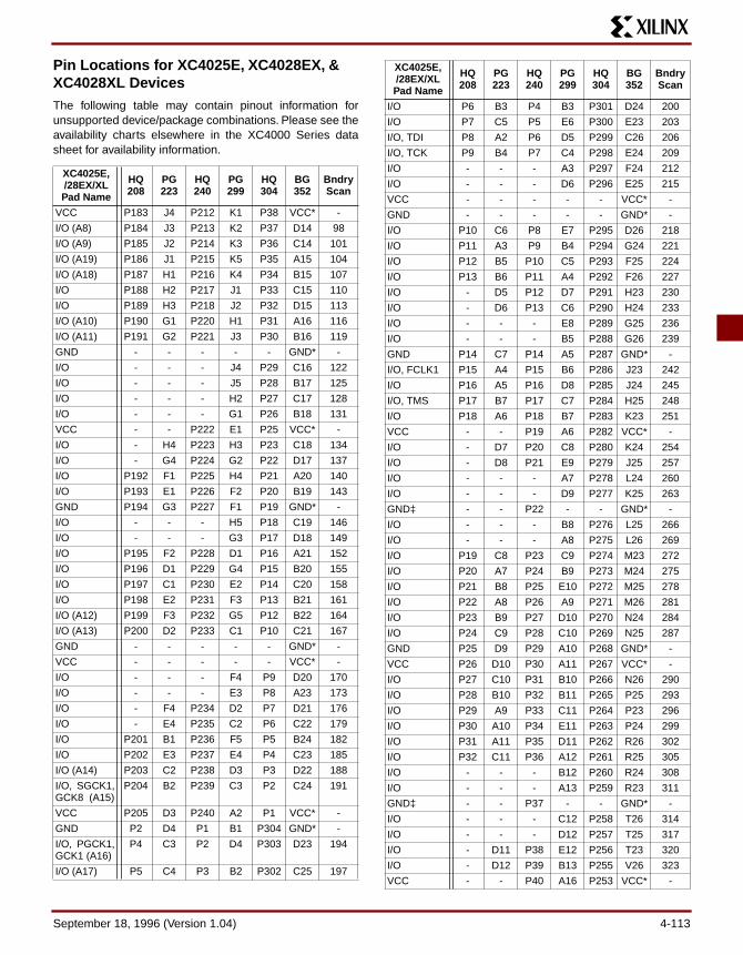
Pin Locations for XC4025E, XC4028EX, & XC4028XL DevicesThe following table may contain pinout information forunsupported device/package combinations. Please see theavailability charts elsewhere in the XC4000 Series datasheet for availability information.
XC4025E,/28EX/XLPad Name
HQ208
PG223
HQ240
PG299
HQ304
BG352
BndryScan
VCC P183 J4 P212 K1 P38 VCC* -
I/O (A8) P184 J3 P213 K2 P37 D14 98
I/O (A9) P185 J2 P214 K3 P36 C14 101
I/O (A19) P186 J1 P215 K5 P35 A15 104
I/O (A18) P187 H1 P216 K4 P34 B15 107
I/O P188 H2 P217 J1 P33 C15 110
I/O P189 H3 P218 J2 P32 D15 113
I/O (A10) P190 G1 P220 H1 P31 A16 116
I/O (A11) P191 G2 P221 J3 P30 B16 119
GND - - - - - GND* -
I/O - - - J4 P29 C16 122
I/O - - - J5 P28 B17 125
I/O - - - H2 P27 C17 128
I/O - - - G1 P26 B18 131
VCC - - P222 E1 P25 VCC* -
I/O - H4 P223 H3 P23 C18 134
I/O - G4 P224 G2 P22 D17 137
I/O P192 F1 P225 H4 P21 A20 140
I/O P193 E1 P226 F2 P20 B19 143
GND P194 G3 P227 F1 P19 GND* -
I/O - - - H5 P18 C19 146
I/O - - - G3 P17 D18 149
I/O P195 F2 P228 D1 P16 A21 152
I/O P196 D1 P229 G4 P15 B20 155
I/O P197 C1 P230 E2 P14 C20 158
I/O P198 E2 P231 F3 P13 B21 161
I/O (A12) P199 F3 P232 G5 P12 B22 164
I/O (A13) P200 D2 P233 C1 P10 C21 167
GND - - - - - GND* -
VCC - - - - - VCC* -
I/O - - - F4 P9 D20 170
I/O - - - E3 P8 A23 173
I/O - F4 P234 D2 P7 D21 176
I/O - E4 P235 C2 P6 C22 179
I/O P201 B1 P236 F5 P5 B24 182
I/O P202 E3 P237 E4 P4 C23 185
I/O (A14) P203 C2 P238 D3 P3 D22 188
I/O, SGCK1, GCK8 (A15)
P204 B2 P239 C3 P2 C24 191
VCC P205 D3 P240 A2 P1 VCC* -
GND P2 D4 P1 B1 P304 GND* -
I/O, PGCK1, GCK1 (A16)
P4 C3 P2 D4 P303 D23 194
I/O (A17) P5 C4 P3 B2 P302 C25 197
I/O P6 B3 P4 B3 P301 D24 200
I/O P7 C5 P5 E6 P300 E23 203
I/O, TDI P8 A2 P6 D5 P299 C26 206
I/O, TCK P9 B4 P7 C4 P298 E24 209
I/O - - - A3 P297 F24 212
I/O - - - D6 P296 E25 215
VCC - - - - - VCC* -
GND - - - - - GND* -
I/O P10 C6 P8 E7 P295 D26 218
I/O P11 A3 P9 B4 P294 G24 221
I/O P12 B5 P10 C5 P293 F25 224
I/O P13 B6 P11 A4 P292 F26 227
I/O - D5 P12 D7 P291 H23 230
I/O - D6 P13 C6 P290 H24 233
I/O - - - E8 P289 G25 236
I/O - - - B5 P288 G26 239
GND P14 C7 P14 A5 P287 GND* -
I/O, FCLK1 P15 A4 P15 B6 P286 J23 242
I/O P16 A5 P16 D8 P285 J24 245
I/O, TMS P17 B7 P17 C7 P284 H25 248
I/O P18 A6 P18 B7 P283 K23 251
VCC - - P19 A6 P282 VCC* -
I/O - D7 P20 C8 P280 K24 254
I/O - D8 P21 E9 P279 J25 257
I/O - - - A7 P278 L24 260
I/O - - - D9 P277 K25 263
GND‡ - - P22 - - GND* -
I/O - - - B8 P276 L25 266
I/O - - - A8 P275 L26 269
I/O P19 C8 P23 C9 P274 M23 272
I/O P20 A7 P24 B9 P273 M24 275
I/O P21 B8 P25 E10 P272 M25 278
I/O P22 A8 P26 A9 P271 M26 281
I/O P23 B9 P27 D10 P270 N24 284
I/O P24 C9 P28 C10 P269 N25 287
GND P25 D9 P29 A10 P268 GND* -
VCC P26 D10 P30 A11 P267 VCC* -
I/O P27 C10 P31 B10 P266 N26 290
I/O P28 B10 P32 B11 P265 P25 293
I/O P29 A9 P33 C11 P264 P23 296
I/O P30 A10 P34 E11 P263 P24 299
I/O P31 A11 P35 D11 P262 R26 302
I/O P32 C11 P36 A12 P261 R25 305
I/O - - - B12 P260 R24 308
I/O - - - A13 P259 R23 311
GND‡ - - P37 - - GND* -
I/O - - - C12 P258 T26 314
I/O - - - D12 P257 T25 317
I/O - D11 P38 E12 P256 T23 320
I/O - D12 P39 B13 P255 V26 323
VCC - - P40 A16 P253 VCC* -
XC4025E,/28EX/XLPad Name
HQ208
PG223
HQ240
PG299
HQ304
BG352
BndryScan
September 18, 1996 (Version 1.04) 4-113

XC4000 Series Field Programmable Gate Arrays
I/O P33 B11 P41 A14 P252 U24 326
I/O P34 A12 P42 C13 P251 V25 329
I/O P35 B12 P43 B14 P250 V24 332
I/O, FCLK2 P36 A13 P44 D13 P249 U23 335
GND P37 C12 P45 A15 P248 GND* -
I/O - - - B15 P247 Y26 338
I/O - - - E13 P246 W25 341
I/O - D13 P46 C14 P245 W24 344
I/O - D14 P47 A17 P244 V23 347
I/O P38 B13 P48 D14 P243 AA26 350
I/O P39 A14 P49 B16 P242 Y25 353
I/O P40 A15 P50 C15 P241 Y24 356
I/O P41 C13 P51 E14 P240 AA25 359
GND - - - - - GND* -
VCC - - - - - VCC* -
I/O - - - A18 P239 AB25 362
I/O - - - D15 P238 AA24 365
I/O P42 B14 P52 C16 P237 Y23 368
I/O P43 A16 P53 B17 P236 AC26 371
I/O P44 B15 P54 B18 P235 AA23 374
I/O P45 C14 P55 E15 P234 AB24 377
I/O P46 A17 P56 D16 P233 AD25 380
I/O, SGCK2, GCK2
P47 B16 P57 C17 P232 AC24 383
O (M1) P48 C15 P58 A20 P231 AB23 386
GND P49 D15 P59 A19 P230 GND* -
I (M0) P50 A18 P60 C18 P229 AD24 389
VCC P55 D16 P61 B20 P228 VCC* -
I (M2) P56 C16 P62 D17 P227 AC23 390
I/O, PGCK2, GCK3
P57 B17 P63 B19 P226 AE24 391
I/O (HDC) P58 E16 P64 C19 P225 AD23 394
I/O P59 C17 P65 F16 P224 AC22 397
I/O P60 D17 P66 E17 P223 AF24 400
I/O P61 B18 P67 D18 P222 AD22 403
I/O (LDC) P62 E17 P68 C20 P221 AE23 406
I/O - - - F17 P220 AE22 409
I/O - - - G16 P219 AF23 412
VCC - - - - - VCC* -
GND - - - - - GND* -
I/O P63 F16 P69 D19 P218 AD20 415
I/O P64 C18 P70 E18 P217 AE21 418
I/O P65 D18 P71 D20 P216 AF21 421
I/O P66 F17 P72 G17 P215 AC19 424
I/O - E15 P73 F18 P214 AD19 427
I/O - F15 P74 H16 P213 AE20 430
I/O - - - E19 P212 AF20 433
I/O - - - F19 P211 AC18 436
GND P67 G16 P75 E20 P210 GND* -
I/O P68 E18 P76 H17 P209 AD18 439
I/O P69 F18 P77 G18 P208 AE19 442
XC4025E,/28EX/XLPad Name
HQ208
PG223
HQ240
PG299
HQ304
BG352
BndryScan
I/O P70 G17 P78 G19 P207 AC17 445
I/O P71 G18 P79 H18 P206 AD17 448
VCC - - P80 F20 P204 VCC* -
I/O P72 H16 P81 J16 P203 AE18 451
I/O P73 H17 P82 G20 P202 AF18 454
I/O - - - J17 P201 AE17 457
I/O - - - H19 P200 AE16 460
GND‡ - - P83 - - GND* -
I/O - - - H20 P199 AF16 463
I/O - - - J18 P198 AC15 466
I/O - G15 P84 J19 P197 AD15 469
I/O - H15 P85 K16 P196 AE15 472
I/O P74 H18 P86 J20 P195 AF15 475
I/O P75 J18 P87 K17 P194 AD14 478
I/O P76 J17 P88 K18 P193 AE14 481
I/O (INIT) P77 J16 P89 K19 P192 AF14 484
VCC P78 J15 P90 L20 P191 VCC* -
GND P79 K15 P91 K20 P190 GND* -
I/O P80 K16 P92 L19 P189 AE13 487
I/O P81 K17 P93 L18 P188 AC13 490
I/O P82 K18 P94 L16 P187 AD13 493
I/O P83 L18 P95 L17 P186 AF12 496
I/O P84 L17 P96 M20 P185 AE12 499
I/O P85 L16 P97 M19 P184 AD12 502
I/O - - - N20 P183 AC12 505
I/O - - - M18 P182 AF11 508
GND‡ - - P98 - - GND* -
I/O - - - M17 P181 AE11 511
I/O - - - M16 P180 AD11 514
I/O - L15 P99 N19 P179 AF9 517
I/O - M15 P100 P20 P178 AD10 520
VCC - - P101 T20 P177 VCC* -
I/O P86 M18 P102 N18 P175 AE9 523
I/O P87 M17 P103 P19 P174 AD9 526
I/O P88 N18 P104 N17 P173 AC10 529
I/O P89 P18 P105 R19 P172 AF7 532
GND P90 M16 P106 R20 P171 GND* -
I/O - - - N16 P170 AE8 535
I/O - - - P18 P169 AD8 538
I/O - N15 P107 U20 P168 AC9 541
I/O - P15 P108 P17 P167 AF6 544
I/O P91 N17 P109 T19 P166 AE7 547
I/O P92 R18 P110 R18 P165 AD7 550
I/O P93 T18 P111 P16 P164 AE6 553
I/O P94 P17 P112 V20 P163 AE5 556
GND - - - - - GND* -
VCC - - - - - VCC* -
I/O - - - R17 P162 AD6 559
I/O - - - T18 P161 AC7 562
I/O P95 N16 P113 U19 P160 AF4 565
I/O P96 T17 P114 V19 P159 AF3 568
XC4025E,/28EX/XLPad Name
HQ208
PG223
HQ240
PG299
HQ304
BG352
BndryScan
4-114 September 18, 1996 (Version 1.04)

I/O P97 R17 P115 R16 P158 AD5 571
I/O P98 P16 P116 T17 P157 AE3 574
I/O P99 U18 P117 U18 P156 AD4 577
I/O, SGCK3, GCK4
P100 T16 P118 X20 P155 AC5 580
GND P101 R16 P119 W20 P154 GND* -
DONE P103 U17 P120 V18 P153 AD3 -
VCC P106 R15 P121 X19 P152 VCC* -
PROGRAM P108 V18 P122 U17 P151 AC4 -
I/O (D7) P109 T15 P123 W19 P150 AD2 583
I/O, PGCK3, GCK5
P110 U16 P124 W18 P149 AC3 586
I/O P111 T14 P125 T15 P148 AB4 589
I/O P112 U15 P126 U16 P147 AD1 592
I/O - R14 P127 V17 P146 AA4 595
I/O - R13 P128 X18 P145 AA3 598
I/O - - - U15 P144 AB2 601
I/O - - - T14 P143 AC1 604
VCC - - - - - VCC* -
GND - - - - - GND* -
I/O (D6) P113 V17 P129 W17 P142 Y3 607
I/O P114 V16 P130 V16 P141 AA2 610
I/O P115 T13 P131 X17 P140 AA1 613
I/O P116 U14 P132 U14 P139 W4 616
I/O P117 V15 P133 V15 P138 W3 619
I/O P118 V14 P134 T13 P137 Y2 622
I/O - - - W16 P136 Y1 625
I/O - - - W15 P135 V4 628
GND P119 T12 P135 X16 P134 GND* -
I/O - R12 P136 U13 P133 V3 631
I/O - R11 P137 V14 P132 W2 634
I/O, FCLK3 P120 U13 P138 W14 P131 U4 637
I/O P121 V13 P139 V13 P130 U3 640
VCC - - P140 X15 P129 VCC* -
I/O (D5) P122 U12 P141 T12 P127 V2 643
I/O (CS0) P123 V12 P142 X14 P126 V1 646
GND‡ - - P143 - - - -
I/O - - - U12 P125 U2 649
I/O - - - W13 P124 T2 652
GND - - - - - GND* -
I/O - - - X13 P123 T1 655
I/O - - - V12 P122 R4 658
I/O P124 T11 P144 W12 P121 R3 661
I/O P125 U11 P145 T11 P120 R2 664
I/O P126 V11 P146 X12 P119 R1 667
I/O P127 V10 P147 U11 P118 P3 670
I/O (D4) P128 U10 P148 V11 P117 P2 673
I/O P129 T10 P149 W11 P116 P1 676
VCC P130 R10 P150 X10 P115 VCC* -
GND P131 R9 P151 X11 P114 GND* -
I/O (D3) P132 T9 P152 W10 P113 N2 679
XC4025E,/28EX/XLPad Name
HQ208
PG223
HQ240
PG299
HQ304
BG352
BndryScan
I/O (RS) P133 U9 P153 V10 P112 N4 682
I/O P134 V9 P154 T10 P111 N3 685
I/O P135 V8 P155 U10 P110 M1 688
I/O P136 U8 P156 X9 P109 M2 691
I/O P137 T8 P157 W9 P108 M3 694
I/O - - - X8 P107 M4 697
I/O - - - V9 P106 L1 700
GND‡ - - P158 - - GND* -
I/O - - - U9 P105 L2 703
I/O - - - T9 P104 L3 706
I/O (D2) P138 V7 P159 W8 P103 J1 709
I/O P139 U7 P160 X7 P102 K3 712
VCC - - P161 X5 P101 VCC* -
I/O P140 V6 P162 V8 P99 J2 715
I/O, FCLK4 P141 U6 P163 W7 P98 J3 718
I/O - R8 P164 U8 P97 K4 721
I/O - R7 P165 W6 P96 G1 724
GND P142 T7 P166 X6 P95 GND* -
I/O - - - T8 P94 H2 727
I/O - - - V7 P93 H3 730
I/O - R6 P167 X4 P92 J4 733
I/O - R5 P168 U7 P91 F1 736
I/O P143 V5 P169 W5 P90 G2 739
I/O P144 V4 P170 V6 P89 G3 742
I/O P145 U5 P171 T7 P88 F2 745
I/O P146 T6 P172 X3 P87 E2 748
GND - - - - - GND* -
VCC - - - - - VCC* -
I/O (D1) P147 V3 P173 U6 P86 F3 751
I/O (RCLK,RDY/BUSY)
P148 V2 P174 V5 P85 G4 754
I/O - - - W4 P84 D2 757
I/O - - - W3 P83 F4 760
I/O P149 U4 P175 T6 P82 E3 763
I/O P150 T5 P176 U5 P81 C2 766
I/O (D0, DIN)
P151 U3 P177 V4 P80 D3 769
I/O, SGCK4, GCK6 (DOUT)
P152 T4 P178 X1 P79 E4 772
CCLK P153 V1 P179 V3 P78 C3 -
VCC P154 R4 P180 W1 P77 VCC* -
O, TDO P159 U2 P181 U4 P76 D4 0
GND P160 R3 P182 X2 P75 GND* -
I/O (A0, WS) P161 T3 P183 W2 P74 B3 2
I/O, PGCK4, GCK7 (A1)
P162 U1 P184 V2 P73 C4 5
I/O P163 P3 P185 R5 P72 D5 8
I/O P164 R2 P186 T4 P71 A3 11
I/O (CS1, A2)
P165 T2 P187 U3 P70 D6 14
I/O (A3) P166 N3 P188 V1 P69 C6 17
XC4025E,/28EX/XLPad Name
HQ208
PG223
HQ240
PG299
HQ304
BG352
BndryScan
September 18, 1996 (Version 1.04) 4-115

XC4000 Series Field Programmable Gate Arrays
4/2/96
Pads labelled GND* are internally bonded to a Ground plane within the BG352 package. They have no direct con-nection to any specific package pin.
Pads labelled VCC* are internally bonded to a Vcc plane within the BG352 package. They have no direct connection to any specific package pin.
Pads labelled GND‡ should be connected to Ground if pos-sible; however, they can be left unconnected if necessary for compatibility with other devices.
Additional No Connect (N.C.) Connections on HQ208 Package
3/15/96
Additional Ground (GND) Connections on HQ240 Package
3/21/96
The Ground (GND) package pins in the above table should be externally connected to Ground if possible; however, they can be left unconnected if necessary for compatibility with other devices.
Additional No Connect (N.C.) Connections on HQ304 Package
3/21/96
Note: In XC4025 (no extension) devices in the HQ304 package, P101 is a No Connect (N.C.) pin. P101 is Vcc in XC4025E/L and XC4028EX/XL devices. Where necessary for compatibility, this pin can be left unconnected.
I/O - - - R4 P68 B5 20
I/O - - - P5 P67 A4 23
VCC - - - - - VCC* -
GND - - - - - GND* -
I/O - P4 P189 U2 P66 C7 26
I/O - N4 P190 T3 P65 B6 29
I/O P167 P2 P191 U1 P64 A6 32
I/O P168 T1 P192 P4 P63 D8 35
I/O P169 R1 P193 R3 P62 B7 38
I/O P170 N2 P194 N5 P61 A7 41
I/O - - P195 T2 P60 D9 44
I/O - - - R2 P59 C9 47
GND P171 M3 P196 T1 P58 GND* -
I/O P172 P1 P197 N4 P57 B8 50
I/O P173 N1 P198 P3 P56 D10 53
I/O - M4 P199 P2 P55 C10 56
I/O - L4 P200 N3 P54 B9 59
VCC - - P201 R1 P52 VCC* -
I/O - - - M5 P51 A9 62
I/O - - - P1 P50 D11 65
I/O - - - M4 P49 B11 68
I/O - - - N2 P48 A11 71
GND - - - - - GND* -
I/O (A4) P174 M2 P202 N1 P47 D12 74
I/O (A5) P175 M1 P203 M3 P46 C12 77
I/O P176 L3 P205 M2 P45 B12 80
I/O P177 L2 P206 L5 P44 A12 83
I/O (A21) P178 L1 P207 M1 P43 C13 86
I/O (A20) P179 K1 P208 L4 P42 B13 89
I/O (A6) P180 K2 P209 L3 P41 A13 92
I/O (A7) P181 K3 P210 L2 P40 B14 95
GND P182 K4 P211 L1 P39 GND* -
XC4025E,/28EX/XLPad Name
HQ208
PG223
HQ240
PG299
HQ304
BG352
BndryScan
N.C. N.C.
P1 P107
P3 P155
P51 P156
P52 P157
P53 P158
P54 P206
P102 P207
P104 P208
P105
GND
P204
P219
N.C.
P11
P24
P53
P100
P128
P176
P205
P254
P281
4-116 September 18, 1996 (Version 1.04)
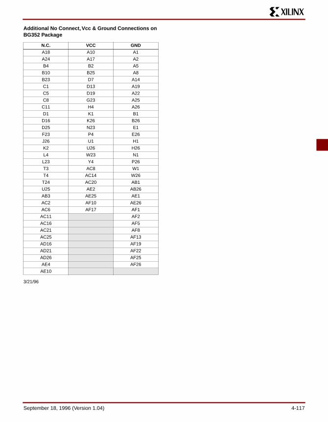
Additional No Connect, Vcc & Ground Connections on BG352 Package
3/21/96
N.C. VCC GND
A18 A10 A1
A24 A17 A2
B4 B2 A5
B10 B25 A8
B23 D7 A14
C1 D13 A19
C5 D19 A22
C8 G23 A25
C11 H4 A26
D1 K1 B1
D16 K26 B26
D25 N23 E1
F23 P4 E26
J26 U1 H1
K2 U26 H26
L4 W23 N1
L23 Y4 P26
T3 AC8 W1
T4 AC14 W26
T24 AC20 AB1
U25 AE2 AB26
AB3 AE25 AE1
AC2 AF10 AE26
AC6 AF17 AF1
AC11 AF2
AC16 AF5
AC21 AF8
AC25 AF13
AD16 AF19
AD21 AF22
AD26 AF25
AE4 AF26
AE10
September 18, 1996 (Version 1.04) 4-117

XC4000 Series Field Programmable Gate Arrays
Pin Locations for XC4036EX/XL DevicesThe following table may contain pinout information forunsupported device/package combinations. Please see theavailability charts elsewhere in the XC4000 Series datasheet for availability information.
XC4036EX/XLPad Name
HQ304 PG411 BG432Bndry Scan
GND P304 GND* GND* -I/O, GCK1 (A16) P303 H8 D29 218I/O (A17) P302 F6 C30 221I/O P301 B4 E28 224I/O P300 D4 E29 227I/O, TDI P299 B2 D30 230I/O, TCK P298 G9 D31 233I/O - F8 E30 236I/O - C5 E31 239I/O P297 A7 G28 242I/O P296 A5 G29 245VCC - VCC* VCC* -GND - GND* GND* -I/O P295 B8 H28 248I/O P294 C9 H29 251I/O P293 E9 G30 254I/O P292 F12 H30 257I/O P291 D10 J28 260I/O P290 B10 J29 263I/O P289 F10 H31 266I/O P288 F14 J30 269GND P287 GND* GND* -I/O, FCLK1 P286 C11 K28 272I/O P285 B12 K29 275I/O, TMS P284 E11 K30 278I/O P283 E15 K31 281VCC P282 VCC* VCC* -I/O P280 F16 L29 284I/O P279 C13 L30 287I/O - B14 M29 290I/O - E17 M31 293I/O P278 E13 N31 296I/O P277 A15 N28 299GND - GND* GND* -VCC - VCC* VCC* -I/O P276 B16 P30 302I/O P275 D16 P28 305I/O P274 D18 P29 308I/O P273 A17 R31 311I/O P272 E19 R30 314I/O P271 B18 R28 317I/O P270 C17 R29 320
I/O P269 C19 T31 323GND P268 GND* GND* -VCC P267 VCC* VCC* -I/O P266 F20 T30 326I/O P265 B20 T29 329I/O P264 C21 U31 332I/O P263 B22 U30 335I/O P262 E21 U28 338I/O P261 D22 U29 341I/O P260 A23 V30 344I/O P259 B24 V29 347VCC - VCC* VCC* -GND - GND* GND* -I/O P258 A25 W30 350I/O P257 D24 W29 353I/O - B26 Y30 356I/O - A27 Y29 359I/O P256 C27 Y28 362I/O P255 F24 AA30 365VCC P253 VCC* VCC* -I/O P252 E25 AA29 368I/O P251 E27 AB31 371I/O P250 B28 AB30 374I/O, FCLK2 P249 C29 AB29 377GND P248 GND* GND* -I/O P247 F26 AB28 380I/O P246 D28 AC30 383I/O P245 B30 AC29 386I/O P244 E29 AC28 389I/O P243 F28 AD29 392I/O P242 F30 AD28 395I/O P241 C31 AE30 398I/O P240 E31 AE29 401GND - GND* GND* -VCC - VCC* VCC* -I/O P239 B32 AF31 404I/O P238 A33 AE28 407I/O P237 A35 AG31 410I/O P236 F32 AF28 413I/O - C35 AG30 416I/O - B38 AG29 419I/O P235 E33 AH31 422I/O P234 G31 AG28 425I/O P233 H32 AH30 428I/O, GCK2 P232 B36 AJ30 431O (M1) P231 A39 AH29 434GND P230 GND* GND* -
XC4036EX/XLPad Name
HQ304 PG411 BG432Bndry Scan
4-118 September 18, 1996 (Version 1.04)

I (M0) P229 E35 AH28 437VCC P228 VCC* VCC* -I (M2) P227 G33 AJ28 438I/O, GCK3 P226 D36 AK29 439I/O (HDC) P225 C37 AH27 442I/O P224 F34 AK28 445I/O P223 J33 AJ27 448I/O P222 D38 AL28 451I/O (LDC) P221 G35 AH26 454I/O - E39 AL27 457I/O - K34 AH25 460I/O P220 F38 AK26 463I/O P219 G37 AL26 466VCC - VCC* VCC* -GND - GND* GND* -I/O P218 H38 AH24 469I/O P217 J37 AJ25 472I/O P216 G39 AK25 475I/O P215 M34 AJ24 478I/O P214 N35 AL24 481I/O P213 P34 AH22 484I/O P212 J35 AJ23 487I/O P211 L37 AK23 490GND P210 GND* GND* -I/O P209 M38 AJ22 493I/O P208 R35 AK22 496I/O P207 H36 AL22 499I/O P206 T34 AJ21 502VCC P204 VCC* VCC* -I/O P203 N37 AH20 505I/O P202 N39 AK21 508I/O - U35 AK20 511I/O - R39 AJ19 514I/O P201 M36 AL20 517I/O P200 V34 AH18 520GND - GND* GND* -VCC - VCC* VCC* -I/O P199 R37 AK19 523I/O P198 T38 AJ18 526I/O P197 T36 AL19 529I/O P196 V36 AK18 532I/O P195 U37 AH17 535I/O P194 U39 AJ17 538I/O P193 V38 AJ16 541I/O (INIT) P192 W37 AK16 544VCC P191 VCC* VCC* -GND P190 GND* GND* -
XC4036EX/XLPad Name
HQ304 PG411 BG432Bndry Scan
I/O P189 Y34 AL16 547I/O P188 AC37 AH15 550I/O P187 AB38 AK15 553I/O P186 AD36 AJ14 556I/O P185 AA35 AH14 559I/O P184 AE37 AK14 562I/O P183 AB36 AL13 565I/O P182 AD38 AK13 568VCC - VCC* VCC* -GND - GND* GND* -I/O P181 AB34 AJ13 571I/O P180 AE39 AH13 574I/O - AM36 AL12 577I/O - AC35 AK12 580I/O P179 AG39 AH12 583I/O P178 AG37 AJ11 586VCC P177 VCC* VCC* -I/O P175 AD34 AL10 589I/O P174 AN39 AK10 592I/O P173 AE35 AJ10 595I/O P172 AH38 AK9 598GND P171 GND* GND* -I/O P170 AJ37 AL8 601I/O P169 AG35 AH10 604I/O P168 AF34 AJ9 607I/O P167 AH36 AK8 610I/O P166 AK36 AK7 613I/O P165 AM34 AL6 616I/O P164 AH34 AJ7 619I/O P163 AJ35 AH8 622GND - GND* GND* -VCC - VCC* VCC* -I/O P162 AL37 AK6 625I/O P161 AT38 AL5 628I/O P160 AM38 AH7 631I/O P159 AN37 AJ6 634I/O - AK34 AK5 637I/O - AR39 AL4 640I/O P158 AN35 AK4 643I/O P157 AL33 AH5 646I/O P156 AV38 AK3 649I/O, GCK4 P155 AT36 AJ4 652GND P154 GND* GND* -DONE P153 AR35 AH4 -VCC P152 VCC* VCC* -PROGRAM P151 AN33 AH3 -I/O (D7) P150 AM32 AJ2 655
XC4036EX/XLPad Name
HQ304 PG411 BG432Bndry Scan
September 18, 1996 (Version 1.04) 4-119

XC4000 Series Field Programmable Gate Arrays
I/O, GCK5 P149 AP34 AG4 658I/O P148 AW39 AG3 661I/O P147 AN31 AH2 664I/O - AV36 AH1 667I/O - AR33 AF4 670I/O P146 AP32 AF3 673I/O P145 AU35 AG2 676I/O P144 AW33 AE3 679I/O P143 AU33 AF2 682VCC - VCC* VCC* -GND - GND* GND* -I/O (D6) P142 AV32 AF1 685I/O P141 AU31 AD4 688I/O P140 AR31 AD3 691I/O P139 AP28 AE2 694I/O P138 AT32 AC3 697I/O P137 AV30 AD1 700I/O P136 AR29 AC2 703I/O P135 AP26 AB4 706GND P134 GND* GND* -I/O P133 AU29 AB3 709I/O P132 AV28 AB2 712I/O, FCLK3 P131 AT28 AB1 715I/O P130 AR25 AA3 718VCC P129 VCC* VCC* -I/O (D5) P127 AP24 AA2 721I/O (CS0) P126 AU27 Y2 724I/O - AR27 Y4 727I/O - AW27 Y3 730I/O P125 AT24 W4 733I/O P124 AR23 W3 736GND - GND* GND* -VCC - VCC* VCC* -I/O P123 AP22 V4 739I/O P122 AV24 V3 742I/O P121 AU23 U1 745I/O P120 AT22 U2 748I/O P119 AR21 U4 751I/O P118 AV22 U3 754I/O (D4) P117 AP20 T1 757I/O P116 AU21 T2 760VCC P115 VCC* VCC* -GND P114 GND* GND* -I/O (D3) P113 AU19 T3 763I/O (RS) P112 AV20 R1 766I/O P111 AV18 R2 769I/O P110 AR19 R4 772
XC4036EX/XLPad Name
HQ304 PG411 BG432Bndry Scan
I/O P109 AT18 R3 775I/O P108 AW17 P2 778I/O P107 AV16 P3 781I/O P106 AP18 P4 784VCC - VCC* VCC* -GND - GND* GND* -I/O P105 AR17 N3 787I/O P104 AT16 N4 790I/O - AV14 M1 793I/O - AW13 M2 796I/O (D2) P103 AR15 L2 799I/O P102 AP16 L3 802VCC P101 VCC* VCC* -I/O P99 AV12 K1 805I/O, FCLK4 P98 AR13 K2 808I/O P97 AU11 K3 811I/O P96 AT12 K4 814GND P95 GND* GND* -I/O P94 AP14 J2 817I/O P93 AR11 J3 820I/O P92 AV10 J4 823I/O P91 AT8 H1 826I/O P90 AT10 H2 829I/O P89 AP10 H3 832I/O P88 AP12 H4 835I/O P87 AR9 G2 838GND - GND* GND* -VCC - VCC* VCC* -I/O (D1) P86 AU7 G4 841I/O (RCLK, RDY/BUSY)
P85 AW7 F2 844
I/O - AW5 F3 847I/O - AV6 E1 850I/O P84 AR7 E3 853I/O P83 AV4 D1 856I/O P82 AN9 E4 859I/O P81 AW1 D2 862I/O (D0, DIN) P80 AP6 C2 865I/O, GCK6 (DOUT) P79 AU3 D3 868CCLK P78 AR5 D4 -VCC P77 VCC* VCC* -O, TDO P76 AN7 C4 0GND P75 GND* GND* -I/O (A0, WS) P74 AT4 B3 2I/O, GCK7 (A1) P73 AV2 D5 5I/O P72 AM8 B4 8I/O P71 AL7 C5 11
XC4036EX/XLPad Name
HQ304 PG411 BG432Bndry Scan
4-120 September 18, 1996 (Version 1.04)

4/2/96
Pads labelled GND* are internally bonded to a Ground plane within the associated package. They have no direct connection to any specific package pin.
Pads labelled VCC* are internally bonded to a Vcc plane within the associated package. They have no direct con-nection to any specific package pin.
I/O - AR3 B5 14I/O - AR1 C6 17I/O (CS1, A2) P70 AK6 A5 20I/O (A3) P69 AN3 D7 23I/O P68 AM6 B6 26I/O P67 AM2 A6 29VCC - VCC* VCC* -GND - GND* GND* -I/O P66 AL3 D8 32I/O P65 AH6 C7 35I/O P64 AP2 B7 38I/O P63 AK4 D9 41I/O P62 AG5 D10 44I/O P61 AF6 C9 47I/O P60 AL5 B9 50I/O P59 AJ3 C10 53GND P58 GND* GND* -I/O P57 AH2 B10 56I/O P56 AE5 A10 59I/O P55 AM4 C11 62I/O P54 AD6 D12 65VCC P52 VCC* VCC* -I/O P51 AG3 B11 68I/O P50 AG1 C12 71I/O - AC5 C13 74I/O - AE1 A12 77I/O P49 AH4 D14 80I/O P48 AB6 B13 83GND - GND* GND* -VCC - VCC* VCC* -I/O (A4) P47 AD2 C14 86I/O (A5) P46 AB4 A13 89I/O P45 AE3 B14 92I/O P44 AC1 D15 95I/O (A21) P43 AD4 C15 98I/O (A20) P42 AA5 B15 101I/O (A6) P41 AA3 B16 104I/O (A7) P40 Y6 A16 107GND P39 GND* GND* -VCC P38 VCC* VCC* -I/O (A8) P37 W3 D17 110I/O (A9) P36 Y2 A17 113I/O (A19) P35 V4 C18 116I/O (A18) P34 T2 D18 119I/O P33 U1 B18 122I/O P32 V6 A19 125
XC4036EX/XLPad Name
HQ304 PG411 BG432Bndry Scan
I/O (A10) P31 U3 B19 128I/O (A11) P30 R1 C19 131VCC - VCC* VCC* -GND - GND* GND* -I/O P29 U5 D19 134I/O P28 T4 A20 137I/O - P2 B20 140I/O - N1 C20 143I/O P27 R5 C21 146I/O P26 M2 A22 149VCC P25 VCC* VCC* -I/O P23 L3 B22 152I/O P22 T6 C22 155I/O P21 N5 B23 158I/O P20 M4 A24 161GND P19 GND* GND* -I/O P18 K2 D22 164I/O P17 K4 C23 167I/O P16 P6 B24 170I/O P15 M6 C24 173I/O P14 J3 A26 176I/O P13 H2 C25 179I/O (A12) P12 H4 D24 182I/O (A13) P10 G3 B26 185GND - GND* GND* -VCC - VCC* VCC* -I/O P9 K6 A27 188I/O P8 G1 D25 191I/O - E1 C26 194I/O - E3 B27 197I/O P7 J7 C27 200I/O P6 H6 B28 203I/O P5 C3 D27 206I/O P4 D2 B29 209I/O (A14) P3 E5 C28 212I/O, GCK8 (A15) P2 G7 D28 215VCC P1 VCC* VCC* -
XC4036EX/XLPad Name
HQ304 PG411 BG432Bndry Scan
September 18, 1996 (Version 1.04) 4-121
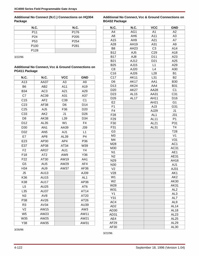
XC4000 Series Field Programmable Gate Arrays
Additional No Connect (N.C.) Connections on HQ304 Package
3/22/96
Additional No Connect, Vcc & Ground Connections on PG411 Package
3/26/96
Additional No Connect, Vcc & Ground Connections on BG432 Package
3/22/96
N.C. N.C.P11 P176P24 P205P53 P254P100 P281P128
N.C. N.C. VCC GNDA13 AA37 A3 A9B6 AB2 A11 A19B34 AC3 A21 A29C7 AC39 A31 A37C15 AF2 C39 C1C23 AF38 D6 D14C25 AJ5 F36 D20C33 AK2 J1 D26D8 AK38 L39 D34D12 AL35 W1 F4D30 AN1 AA39 J39D32 AN5 AJ1 L1E7 AP8 AL39 P4E23 AP30 AP4 P36E37 AP38 AT34 W39F2 AR37 AU1 Y4F18 AT2 AW9 Y36F22 AT30 AW19 AA1G5 AU5 AW29 AF4H34 AU9 AW37 AF36J5 AU13 AJ39
K36 AU15 AL1K38 AU17 AP36L5 AU25 AT6L35 AU37 AT14N3 AV8 AT20P38 AV26 AT26R3 AV34 AU39V2 AW15 AW3W5 AW23 AW11W35 AW25 AW21Y38 AW35 AW31
N.C. N.C. VCC GNDA4 AG1 A1 A2A8 AH6 A11 A3A15 AH9 A21 A7A28 AH19 A31 A9B8 AH23 C3 A14B12 AJ5 C29 A18B17 AJ8 D11 A23B21 AJ12 D21 A25B25 AJ15 L1 A29C8 AJ20 L4 A30C16 AJ26 L28 B1C17 AK11 L31 B2D6 AK17 AA1 B30D13 AK24 AA4 B31D20 AK27 AA28 C1D23 AL15 AA31 C31D26 AL17 AH11 D16E2 AH21 G1F1 AJ3 G31F4 AJ29 J1
F28 AL1 J31F29 AL11 P1F30 AL21 P31F31 AL31 T4G3 T28M3 V1M4 V31M28 AC1M30 AC31N1 AE1N2 AE31N29 AH16N30 AJ1V2 AJ31V28 AK1W1 AK2W2 AK30W28 AK31W31 AL2Y1 AL3Y31 AL7AC4 AL9AD2 AL14AD30 AL18AD31 AL23AE4 AL25AF29 AL29AF30 AL30
4-122 September 18, 1996 (Version 1.04)

Pin Locations for XC4044EX/XL DevicesThe following table may contain pinout information forunsupported device/package combinations. Please see theavailability charts elsewhere in the XC4000 Series datasheet for availability information.
XC4044EX/XLPad Name PG411 BG432 Bndry Scan
GND GND* GND* -
I/O, GCK1 (A16) H8 D29 242
I/O (A17) F6 C30 245
I/O B4 E28 248
I/O D4 E29 251
I/O, TDI B2 D30 254
I/O, TCK G9 D31 257
I/O F8 E30 260
I/O C5 E31 263
I/O A7 G28 266
I/O A5 G29 269
VCC VCC* VCC* -
GND GND* GND* -
I/O C7 F30 272
I/O D8 F31 275
I/O B8 H28 278
I/O C9 H29 281
I/O E9 G30 284
I/O F12 H30 287
I/O D10 J28 290
I/O B10 J29 293
I/O F10 H31 296
I/O F14 J30 299
GND GND* GND* -
I/O, FCLK1 C11 K28 302
I/O B12 K29 305
I/O, TMS E11 K30 308
I/O E15 K31 311
VCC VCC* VCC* -
I/O F16 L29 314
I/O C13 L30 317
I/O B14 M29 320
I/O E17 M31 323
I/O E13 N31 326
I/O A15 N28 329
GND GND* GND* -
VCC VCC* VCC* -
I/O F18 N29 332
I/O C15 N30 335
I/O B16 P30 338
I/O D16 P28 341
I/O D18 P29 344
I/O A17 R31 347
I/O E19 R30 350
I/O B18 R28 353
I/O C17 R29 356
I/O C19 T31 359
GND GND* GND* -
VCC VCC* VCC* -
I/O F20 T30 362
I/O B20 T29 365
I/O C21 U31 368
I/O B22 U30 371
I/O E21 U28 374
I/O D22 U29 377
I/O A23 V30 380
I/O B24 V29 383
I/O C23 V28 386
I/O F22 W31 389
VCC VCC* VCC* -
GND GND* GND* -
I/O A25 W30 392
I/O D24 W29 395
I/O B26 Y30 398
I/O A27 Y29 401
I/O C27 Y28 404
I/O F24 AA30 407
VCC VCC* VCC* -
I/O E25 AA29 410
I/O E27 AB31 413
I/O B28 AB30 416
I/O, FCLK2 C29 AB29 419
GND GND* GND* -
I/O F26 AB28 422
I/O D28 AC30 425
I/O B30 AC29 428
I/O E29 AC28 431
I/O D30 AD31 434
I/O D32 AD30 437
I/O F28 AD29 440
I/O F30 AD28 443
I/O C31 AE30 446
I/O E31 AE29 449
GND GND* GND* -
VCC VCC* VCC* -
I/O B32 AF31 452
I/O A33 AE28 455
I/O A35 AG31 458
I/O F32 AF28 461
I/O C35 AG30 464
I/O B38 AG29 467
I/O E33 AH31 470
I/O G31 AG28 473
I/O H32 AH30 476
I/O, GCK2 B36 AJ30 479
O (M1) A39 AH29 482
GND GND* GND* -
I (M0) E35 AH28 485
XC4044EX/XLPad Name PG411 BG432 Bndry Scan
September 18, 1996 (Version 1.04) 4-123
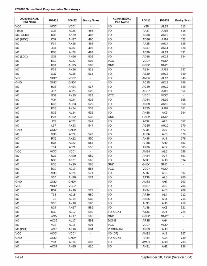
XC4000 Series Field Programmable Gate Arrays
VCC VCC* VCC* -
I (M2) G33 AJ28 486
I/O, GCK3 D36 AK29 487
I/O (HDC) C37 AH27 490
I/O F34 AK28 493
I/O J33 AJ27 496
I/O D38 AL28 499
I/O (LDC) G35 AH26 502
I/O E39 AL27 505
I/O K34 AH25 508
I/O F38 AK26 511
I/O G37 AL26 514
VCC VCC* VCC* -
GND GND* GND* -
I/O H38 AH24 517
I/O J37 AJ25 520
I/O G39 AK25 523
I/O M34 AJ24 526
I/O K36 AH23 529
I/O K38 AK24 532
I/O N35 AL24 535
I/O P34 AH22 538
I/O J35 AJ23 541
I/O L37 AK23 544
GND GND* GND* -
I/O M38 AJ22 547
I/O R35 AK22 550
I/O H36 AL22 553
I/O T34 AJ21 556
VCC VCC* VCC* -
I/O N37 AH20 559
I/O N39 AK21 562
I/O U35 AK20 565
I/O R39 AJ19 568
I/O M36 AL20 571
I/O V34 AH18 574
GND GND* GND* -
VCC VCC* VCC* -
I/O R37 AK19 577
I/O T38 AJ18 580
I/O T36 AL19 583
I/O V36 AK18 586
I/O U37 AH17 589
I/O U39 AJ17 592
I/O W35 AK17 595
I/O AC39 AL17 598
I/O V38 AJ16 601
I/O (INIT) W37 AK16 604
VCC VCC* VCC* -
GND GND* GND* -
I/O Y34 AL16 607
I/O AC37 AH15 610
XC4044EX/XLPad Name PG411 BG432 Bndry Scan
I/O Y38 AL15 613
I/O AA37 AJ15 616
I/O AB38 AK15 619
I/O AD36 AJ14 622
I/O AA35 AH14 625
I/O AE37 AK14 628
I/O AB36 AL13 631
I/O AD38 AK13 634
VCC VCC* VCC* -
GND GND* GND* -
I/O AB34 AJ13 637
I/O AE39 AH13 640
I/O AM36 AL12 643
I/O AC35 AK12 646
I/O AG39 AH12 649
I/O AG37 AJ11 652
VCC VCC* VCC* -
I/O AD34 AL10 655
I/O AN39 AK10 658
I/O AE35 AJ10 661
I/O AH38 AK9 664
GND GND* GND* -
I/O AJ37 AL8 667
I/O AG35 AH10 670
I/O AF34 AJ9 673
I/O AH36 AK8 676
I/O AK38 AJ8 679
I/O AP38 AH9 682
I/O AK36 AK7 685
I/O AM34 AL6 688
I/O AH34 AJ7 691
I/O AJ35 AH8 694
GND GND* GND* -
VCC VCC* VCC* -
I/O AL37 AK6 697
I/O AT38 AL5 700
I/O AM38 AH7 703
I/O AN37 AJ6 706
I/O AK34 AK5 709
I/O AR39 AL4 712
I/O AN35 AK4 715
I/O AL33 AH5 718
I/O AV38 AK3 721
I/O, GCK4 AT36 AJ4 724
GND GND* GND* -
DONE AR35 AH4 -
VCC VCC* VCC* -
PROGRAM AN33 AH3 -
I/O (D7) AM32 AJ2 727
I/O, GCK5 AP34 AG4 730
I/O AW39 AG3 733
I/O AN31 AH2 736
XC4044EX/XLPad Name PG411 BG432 Bndry Scan
4-124 September 18, 1996 (Version 1.04)

I/O AV36 AH1 739
I/O AR33 AF4 742
I/O AP32 AF3 745
I/O AU35 AG2 748
I/O AW33 AE3 751
I/O AU33 AF2 754
VCC VCC* VCC* -
GND GND* GND* -
I/O (D6) AV32 AF1 757
I/O AU31 AD4 760
I/O AR31 AD3 763
I/O AP28 AE2 766
I/O AP30 AD2 769
I/O AT30 AC4 772
I/O AT32 AC3 775
I/O AV30 AD1 778
I/O AR29 AC2 781
I/O AP26 AB4 784
GND GND* GND* -
I/O AU29 AB3 787
I/O AV28 AB2 790
I/O, FCLK3 AT28 AB1 793
I/O AR25 AA3 796
VCC VCC* VCC* -
I/O (D5) AP24 AA2 799
I/O (CS0) AU27 Y2 802
I/O AR27 Y4 805
I/O AW27 Y3 808
I/O AT24 W4 811
I/O AR23 W3 814
GND GND* GND* -
VCC VCC* VCC* -
I/O AW25 W2 817
I/O AW23 V2 820
I/O AP22 V4 823
I/O AV24 V3 826
I/O AU23 U1 829
I/O AT22 U2 832
I/O AR21 U4 835
I/O AV22 U3 838
I/O (D4) AP20 T1 841
I/O AU21 T2 844
VCC VCC* VCC* -
GND GND* GND* -
I/O (D3) AU19 T3 847
I/O (RS) AV20 R1 850
I/O AV18 R2 853
I/O AR19 R4 856
I/O AT18 R3 859
I/O AW17 P2 862
I/O AV16 P3 865
I/O AP18 P4 868
XC4044EX/XLPad Name PG411 BG432 Bndry Scan
I/O AU17 N1 871
I/O AW15 N2 874
VCC VCC* VCC* -
GND GND* GND* -
I/O AR17 N3 877
I/O AT16 N4 880
I/O AV14 M1 883
I/O AW13 M2 886
I/O (D2) AR15 L2 889
I/O AP16 L3 892
VCC VCC* VCC* -
I/O AV12 K1 895
I/O, FCLK4 AR13 K2 898
I/O AU11 K3 901
I/O AT12 K4 904
GND GND* GND* -
I/O AP14 J2 907
I/O AR11 J3 910
I/O AV10 J4 913
I/O AT8 H1 916
I/O AT10 H2 919
I/O AP10 H3 922
I/O AP12 H4 925
I/O AR9 G2 928
I/O AU9 G3 931
I/O AV8 F1 934
GND GND* GND* -
VCC VCC* VCC* -
I/O (D1) AU7 G4 937
I/O (RCLK, RDY/BUSY)
AW7 F2 940
I/O AW5 F3 943
I/O AV6 E1 946
I/O AR7 E3 949
I/O AV4 D1 952
I/O AN9 E4 955
I/O AW1 D2 958
I/O (D0, DIN) AP6 C2 961
I/O, GCK6 (DOUT)
AU3 D3 964
CCLK AR5 D4 -
VCC VCC* VCC* -
O, TDO AN7 C4 0
GND GND* GND* -
I/O (A0, WS) AT4 B3 2
I/O, GCK7 (A1) AV2 D5 5
I/O AM8 B4 8
I/O AL7 C5 11
I/O AR3 B5 14
I/O AR1 C6 17
I/O (CS1, A2) AK6 A5 20
I/O (A3) AN3 D7 23
XC4044EX/XLPad Name PG411 BG432 Bndry Scan
September 18, 1996 (Version 1.04) 4-125

XC4000 Series Field Programmable Gate Arrays
4/2/96
Pads labelled GND* are internally bonded to a Ground plane within the associated package. They have no direct connection to any specific package pin.
Pads labelled VCC* are internally bonded to a Vcc plane within the associated package. They have no direct con-nection to any specific package pin.
I/O AM6 B6 26
I/O AM2 A6 29
VCC VCC* VCC* -
GND GND* GND* -
I/O AL3 D8 32
I/O AH6 C7 35
I/O AP2 B7 38
I/O AK4 D9 41
I/O AN1 B8 44
I/O AK2 A8 47
I/O AG5 D10 50
I/O AF6 C9 53
I/O AL5 B9 56
I/O AJ3 C10 59
GND GND* GND* -
I/O AH2 B10 62
I/O AE5 A10 65
I/O AM4 C11 68
I/O AD6 D12 71
VCC VCC* VCC* -
I/O AG3 B11 74
I/O AG1 C12 77
I/O AC5 C13 80
I/O AE1 A12 83
I/O AH4 D14 86
I/O AB6 B13 89
GND GND* GND* -
VCC VCC* VCC* -
I/O (A4) AD2 C14 92
I/O (A5) AB4 A13 95
I/O AE3 B14 98
I/O AC1 D15 101
I/O (A21) AD4 C15 104
I/O (A20) AA5 B15 107
I/O AB2 A15 110
I/O AC3 C16 113
I/O (A6) AA3 B16 116
I/O (A7) Y6 A16 119
GND GND* GND* -
VCC VCC* VCC* -
I/O (A8) W3 D17 122
I/O (A9) Y2 A17 125
I/O V2 C17 128
I/O W5 B17 131
I/O (A19) V4 C18 134
I/O (A18) T2 D18 137
I/O U1 B18 140
I/O V6 A19 143
I/O (A10) U3 B19 146
I/O (A11) R1 C19 149
VCC VCC* VCC* -
GND GND* GND* -
XC4044EX/XLPad Name PG411 BG432 Bndry Scan
I/O U5 D19 152
I/O T4 A20 155
I/O P2 B20 158
I/O N1 C20 161
I/O R5 C21 164
I/O M2 A22 167
VCC VCC* VCC* -
I/O L3 B22 170
I/O T6 C22 173
I/O N5 B23 176
I/O M4 A24 179
GND GND* GND* -
I/O K2 D22 182
I/O K4 C23 185
I/O P6 B24 188
I/O M6 C24 191
I/O L5 D23 194
I/O J5 B25 197
I/O J3 A26 200
I/O H2 C25 203
I/O (A12) H4 D24 206
I/O (A13) G3 B26 209
GND GND* GND* -
VCC VCC* VCC* -
I/O K6 A27 212
I/O G1 D25 215
I/O E1 C26 218
I/O E3 B27 221
I/O J7 C27 224
I/O H6 B28 227
I/O C3 D27 230
I/O D2 B29 233
I/O (A14) E5 C28 236
I/O, GCK8 (A15) G7 D28 239
VCC VCC* VCC* -
XC4044EX/XLPad Name PG411 BG432 Bndry Scan
4-126 September 18, 1996 (Version 1.04)

Additional No Connect, Vcc & Ground Connections on PG411 Package
3/22/96
Additional No Connect, Vcc & Ground Connections on BG432 Package
3/26/96
N.C. VCC GND
A13 A3 A9
B6 A11 A19
B34 A21 A29
C25 A31 A37
C33 C39 C1
D12 D6 D14
E7 F36 D20
E23 J1 D26
E37 L39 D34
F2 W1 F4
G5 AA39 J39
H34 AJ1 L1
L35 AL39 P4
N3 AP4 P36
P38 AT34 W39
R3 AU1 Y4
AF2 AW9 Y36
AF38 AW19 AA1
AJ5 AW29 AF4
AL35 AW37 AF36
AN5 AJ39
AP8 AL1
AR37 AP36
AT2 AT6
AU5 AT14
AU13 AT20
AU15 AT26
AU25 AU39
AU37 AW3
AV26 AW11
AV34 AW21
AW35 AW31
N.C. VCC GND
A4 A1 A2
A28 A11 A3
B12 A21 A7
B21 A31 A9
C8 C3 A14
D6 C29 A18
D13 D11 A23
D20 D21 A25
D26 L1 A29
E2 L4 A30
F4 L28 B1
F28 L31 B2
F29 AA1 B30
M3 AA4 B31
M4 AA28 C1
M28 AA31 C31
M30 AH11 D16
W1 AH21 G1
W28 AJ3 G31
Y1 AJ29 J1
Y31 AL1 J31
AE4 AL11 P1
AF29 AL21 P31
AF30 AL31 T4
AG1 T28
AH6 V1
AH19 V31
AJ5 AC1
AJ12 AC31
AJ20 AE1
AJ26 AE31
AK11 AH16
AK27 AJ1
AJ31
AK1
AK2
AK30
AK31
AL2
AL3
AL7
AL9
AL14
AL18
AL23
AL25
AL29
AL30
September 18, 1996 (Version 1.04) 4-127

XC4000 Series Field Programmable Gate Arrays
Pin Locations for XC4052XL DevicesThe following table may contain pinout information forunsupported device/package combinations. Please see theavailability charts elsewhere in the XC4000 Series datasheet for availability information.
XC4052XL Pad Name PG411 BG432 Bndry ScanGND GND* GND* -I/O, GCK1 (A16) H8 D29 266I/O (A17) F6 C30 269I/O B4 E28 272I/O D4 E29 275I/O, TDI B2 D30 278I/O, TCK G9 D31 281GND GND* GND* -I/O E7 F28 284I/O B6 F29 287I/O F8 E30 290I/O C5 E31 293I/O A7 G28 296I/O A5 G29 299VCC VCC* VCC* -GND GND* GND* -I/O C7 F30 302I/O D8 F31 305I/O B8 H28 308I/O C9 H29 311I/O E9 G30 314I/O F12 H30 317GND GND* GND* -I/O D10 J28 320I/O B10 J29 323I/O F10 H31 326I/O F14 J30 329GND GND* GND* -I/O, FCLK1 C11 K28 332I/O B12 K29 335I/O, TMS E11 K30 338I/O E15 K31 341VCC VCC* VCC* -I/O F16 L29 344I/O C13 L30 347GND GND* GND* -I/O A13 M30 350I/O D12 M28 353I/O B14 M29 356I/O E17 M31 359I/O E13 N31 362I/O A15 N28 365
GND GND* GND* -VCC VCC* VCC* -I/O F18 N29 368I/O C15 N30 371I/O B16 P30 374I/O D16 P28 377I/O D18 P29 380I/O A17 R31 383GND GND* GND* -I/O E19 R30 386I/O B18 R28 389I/O C17 R29 392I/O C19 T31 395GND GND* GND* -VCC VCC* VCC* -I/O F20 T30 398I/O B20 T29 401I/O C21 U31 404I/O B22 U30 407GND GND* GND* -I/O E21 U28 410I/O D22 U29 413I/O A23 V30 416I/O B24 V29 419I/O C23 V28 422I/O F22 W31 425VCC VCC* VCC* -GND GND* GND* -I/O A25 W30 428I/O D24 W29 431I/O E23 W28 434I/O C25 Y31 437I/O B26 Y30 440I/O A27 Y29 443GND GND* GND* -I/O C27 Y28 446I/O F24 AA30 449VCC VCC* VCC* -I/O E25 AA29 452I/O E27 AB31 455I/O B28 AB30 458I/O, FCLK2 C29 AB29 461GND GND* GND* -I/O F26 AB28 464I/O D28 AC30 467I/O B30 AC29 470I/O E29 AC28 473GND GND* GND* -
XC4052XL Pad Name PG411 BG432 Bndry Scan
4-128 September 18, 1996 (Version 1.04)

I/O D30 AD31 476I/O D32 AD30 479I/O F28 AD29 482I/O F30 AD28 485I/O C31 AE30 488I/O E31 AE29 491GND GND* GND* -VCC VCC* VCC* -I/O B32 AF31 494I/O A33 AE28 497I/O C33 AF30 500I/O B34 AF29 503I/O A35 AG31 506I/O F32 AF28 509GND GND* GND* -I/O C35 AG30 512I/O B38 AG29 515I/O E33 AH31 518I/O G31 AG28 521I/O H32 AH30 524I/O, GCK2 B36 AJ30 527O (M1) A39 AH29 530GND GND* GND* -I (M0) E35 AH28 533VCC VCC* VCC* -I (M2) G33 AJ28 534I/O, GCK3 D36 AK29 535I/O (HDC) C37 AH27 538I/O F34 AK28 541I/O J33 AJ27 544I/O D38 AL28 547I/O (LDC) G35 AH26 550GND GND* GND* -I/O E37 AK27 553I/O H34 AJ26 556I/O E39 AL27 559I/O K34 AH25 562I/O F38 AK26 565I/O G37 AL26 568VCC VCC* VCC* -GND GND* GND* -I/O H38 AH24 571I/O J37 AJ25 574I/O G39 AK25 577I/O M34 AJ24 580I/O K36 AH23 583I/O K38 AK24 586GND GND* GND* -
XC4052XL Pad Name PG411 BG432 Bndry ScanI/O N35 AL24 589I/O P34 AH22 592I/O J35 AJ23 595I/O L37 AK23 598GND GND* GND* -I/O M38 AJ22 601I/O R35 AK22 604I/O H36 AL22 607I/O T34 AJ21 610VCC VCC* VCC* -I/O N37 AH20 613I/O N39 AK21 616GND GND* GND* -I/O P38 AJ20 619I/O L35 AH19 622I/O U35 AK20 625I/O R39 AJ19 628I/O M36 AL20 631I/O V34 AH18 634GND GND* GND* -VCC VCC* VCC* -I/O R37 AK19 637I/O T38 AJ18 640I/O T36 AL19 643I/O V36 AK18 646I/O U37 AH17 649I/O U39 AJ17 652GND GND* GND* -I/O W35 AK17 655I/O AC39 AL17 658I/O V38 AJ16 661I/O (INIT) W37 AK16 664VCC VCC* VCC* -GND GND* GND* -I/O Y34 AL16 667I/O AC37 AH15 670I/O Y38 AL15 673I/O AA37 AJ15 676GND GND* GND* -I/O AB38 AK15 679I/O AD36 AJ14 682I/O AA35 AH14 685I/O AE37 AK14 688I/O AB36 AL13 691I/O AD38 AK13 694VCC VCC* VCC* -GND GND* GND* 697I/O AB34 AJ13 700
XC4052XL Pad Name PG411 BG432 Bndry Scan
September 18, 1996 (Version 1.04) 4-129
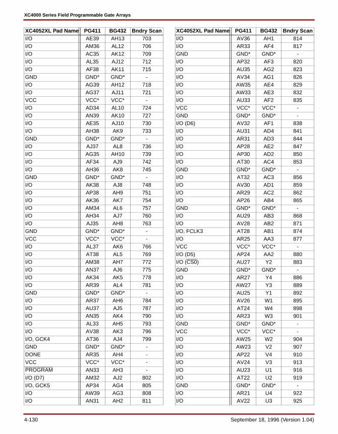
XC4000 Series Field Programmable Gate Arrays
I/O AE39 AH13 703I/O AM36 AL12 706I/O AC35 AK12 709I/O AL35 AJ12 712I/O AF38 AK11 715GND GND* GND* -I/O AG39 AH12 718I/O AG37 AJ11 721VCC VCC* VCC* -I/O AD34 AL10 724I/O AN39 AK10 727I/O AE35 AJ10 730I/O AH38 AK9 733GND GND* GND* -I/O AJ37 AL8 736I/O AG35 AH10 739I/O AF34 AJ9 742I/O AH36 AK8 745GND GND* GND* -I/O AK38 AJ8 748I/O AP38 AH9 751I/O AK36 AK7 754I/O AM34 AL6 757I/O AH34 AJ7 760I/O AJ35 AH8 763GND GND* GND* -VCC VCC* VCC* -I/O AL37 AK6 766I/O AT38 AL5 769I/O AM38 AH7 772I/O AN37 AJ6 775I/O AK34 AK5 778I/O AR39 AL4 781GND GND* GND* -I/O AR37 AH6 784I/O AU37 AJ5 787I/O AN35 AK4 790I/O AL33 AH5 793I/O AV38 AK3 796I/O, GCK4 AT36 AJ4 799GND GND* GND* -DONE AR35 AH4 -VCC VCC* VCC* -PROGRAM AN33 AH3 -I/O (D7) AM32 AJ2 802I/O, GCK5 AP34 AG4 805I/O AW39 AG3 808I/O AN31 AH2 811
XC4052XL Pad Name PG411 BG432 Bndry ScanI/O AV36 AH1 814I/O AR33 AF4 817GND GND* GND* -I/O AP32 AF3 820I/O AU35 AG2 823I/O AV34 AG1 826I/O AW35 AE4 829I/O AW33 AE3 832I/O AU33 AF2 835VCC VCC* VCC* -GND GND* GND* -I/O (D6) AV32 AF1 838I/O AU31 AD4 841I/O AR31 AD3 844I/O AP28 AE2 847I/O AP30 AD2 850I/O AT30 AC4 853GND GND* GND* -I/O AT32 AC3 856I/O AV30 AD1 859I/O AR29 AC2 862I/O AP26 AB4 865GND GND* GND* -I/O AU29 AB3 868I/O AV28 AB2 871I/O, FCLK3 AT28 AB1 874I/O AR25 AA3 877VCC VCC* VCC* -I/O (D5) AP24 AA2 880I/O (CS0) AU27 Y2 883GND GND* GND* -I/O AR27 Y4 886I/O AW27 Y3 889I/O AU25 Y1 892I/O AV26 W1 895I/O AT24 W4 898I/O AR23 W3 901GND GND* GND* -VCC VCC* VCC* -I/O AW25 W2 904I/O AW23 V2 907I/O AP22 V4 910I/O AV24 V3 913I/O AU23 U1 916I/O AT22 U2 919GND GND* GND* -I/O AR21 U4 922I/O AV22 U3 925
XC4052XL Pad Name PG411 BG432 Bndry Scan
4-130 September 18, 1996 (Version 1.04)

I/O (D4) AP20 T1 928I/O AU21 T2 931VCC VCC* VCC* -GND GND* GND* -I/O (D3) AU19 T3 934I/O (RS) AV20 R1 937I/O AV18 R2 940I/O AR19 R4 943GND GND* GND* -I/O AT18 R3 946I/O AW17 P2 949I/O AV16 P3 952I/O AP18 P4 955I/O AU17 N1 958I/O AW15 N2 961VCC VCC* VCC* -GND GND* GND* -I/O AR17 N3 964I/O AT16 N4 967I/O AV14 M1 970I/O AW13 M2 973I/O AU15 M3 976I/O AU13 M4 979GND GND* GND* -I/O (D2) AR15 L2 982I/O AP16 L3 985VCC VCC* VCC* -I/O AV12 K1 988I/O, FCLK4 AR13 K2 991I/O AU11 K3 994I/O AT12 K4 997GND GND* GND* -I/O AP14 J2 1000I/O AR11 J3 1003I/O AV10 J4 1006I/O AT8 H1 1009GND GND* GND* -I/O AT10 H2 1012I/O AP10 H3 1015I/O AP12 H4 1018I/O AR9 G2 1021I/O AU9 G3 1024I/O AV8 F1 1027GND GND* GND* -VCC VCC* VCC* -I/O (D1) AU7 G4 1030I/O (RCLK, RDY/BUSY)
AW7 F2 1033
XC4052XL Pad Name PG411 BG432 Bndry ScanI/O AW5 F3 1036I/O AV6 E1 1039I/O AU5 F4 1042I/O AP8 E2 1045GND GND* GND* -I/O AR7 E3 1048I/O AV4 D1 1051I/O AN9 E4 1054I/O AW1 D2 1057I/O (D0, DIN) AP6 C2 1060I/O, GCK6 (DOUT) AU3 D3 1063CCLK AR5 D4 -VCC VCC* VCC* -O, TDO AN7 C4 0GND GND* GND* -I/O (A0, WS) AT4 B3 2I/O, GCK7 (A1) AV2 D5 5I/O AM8 B4 8I/O AL7 C5 11I/O AT2 A4 14I/O AN5 D6 17GND GND* GND* -I/O AR3 B5 20I/O AR1 C6 23I/O (CS1, A2) AK6 A5 26I/O (A3) AN3 D7 29I/O AM6 B6 32I/O AM2 A6 35VCC VCC* VCC* -GND GND* GND* -I/O AL3 D8 38I/O AH6 C7 41I/O AP2 B7 44I/O AK4 D9 47I/O AN1 B8 50I/O AK2 A8 53GND GND* GND* -I/O AG5 D10 56I/O AF6 C9 59I/O AL5 B9 62I/O AJ3 C10 65GND GND* GND* -I/O AH2 B10 68I/O AE5 A10 71I/O AM4 C11 74I/O AD6 D12 77VCC VCC* VCC* -I/O AG3 B11 80
XC4052XL Pad Name PG411 BG432 Bndry Scan
September 18, 1996 (Version 1.04) 4-131

XC4000 Series Field Programmable Gate Arrays
8/23/96
Pads labelled GND* are internally bonded to a Ground plane within the associated package. They have no direct connection to any specific package pin.
Pads labelled VCC* are internally bonded to a Vcc plane within the associated package. They have no direct con-nection to any specific package pin.
I/O AG1 C12 83GND GND* GND* -I/O AF2 D13 86I/O AJ5 B12 89I/O AC5 C13 92I/O AE1 A12 95I/O AH4 D14 98I/O AB6 B13 101GND GND* GND* -VCC VCC* VCC* -I/O (A4) AD2 C14 104I/O (A5) AB4 A13 107I/O AE3 B14 110I/O AC1 D15 113I/O (A21) AD4 C15 116I/O (A20) AA5 B15 119GND GND* GND* -I/O AB2 A15 122I/O AC3 C16 125I/O (A6) AA3 B16 128I/O (A7) Y6 A16 131GND GND* GND* -VCC VCC* VCC* -I/O (A8) W3 D17 134I/O (A9) Y2 A17 137I/O V2 C17 140I/O W5 B17 143GND GND* GND* -I/O (A19) V4 C18 146I/O (A18) T2 D18 149I/O U1 B18 152I/O V6 A19 155I/O (A10) U3 B19 158I/O (A11) R1 C19 161VCC VCC* VCC* -GND GND* GND* -I/O U5 D19 164I/O T4 A20 167I/O P2 B20 170I/O N1 C20 173I/O R3 B21 176I/O N3 D20 179GND GND* GND* -I/O R5 C21 182I/O M2 A22 185VCC VCC* VCC* -I/O L3 B22 188I/O T6 C22 191
XC4052XL Pad Name PG411 BG432 Bndry ScanI/O N5 B23 194I/O M4 A24 197GND GND* GND* -I/O K2 D22 200I/O K4 C23 203I/O P6 B24 206I/O M6 C24 209GND GND* GND* -I/O L5 D23 212I/O J5 B25 215I/O J3 A26 218I/O H2 C25 221I/O (A12) H4 D24 224I/O (A13) G3 B26 227GND GND* GND* -VCC VCC* VCC* -I/O K6 A27 230I/O G1 D25 233I/O E1 C26 236I/O E3 B27 239I/O F2 A28 242I/O G5 D26 245GND GND* GND* -I/O J7 C27 248I/O H6 B28 251I/O C3 D27 254I/O D2 B29 257I/O (A14) E5 C28 260I/O, GCK8 (A15) G7 D28 263VCC VCC* VCC* -
XC4052XL Pad Name PG411 BG432 Bndry Scan
4-132 September 18, 1996 (Version 1.04)

Additional Vcc & Ground Connections on PG411 Package
8/23/96
Additional No Connect, Vcc & Ground Connections on BG432 Package
3/22/96
VCC GND
A3 A9
A11 A19
A21 A29
A31 A37
C39 C1
D6 D14
F36 D20
J1 D26
L39 D34
W1 F4
AA39 J39
AJ1 L1
AL39 P4
AP4 P36
AT34 W39
AU1 Y4
AW9 Y36
AW19 AA1
AW29 AF4
AW37 AF36
AJ39
AL1
AP36
AT6
AT14
AT20
AT26
AU39
AW3
AW11
AW21
AW31
N.C. VCC GND
C8 A1 A2
A11 A3
A21 A7
A31 A9
C3 A14
C29 A18
D11 A23
D21 A25
L1 A29
L4 A30
L28 B1
L31 B2
AA1 B30
AA4 B31
AA28 C1
AA31 C31
AH11 D16
AH21 G1
AJ3 G31
AJ29 J1
AL1 J31
AL11 P1
AL21 P31
AL31 T4
T28
V1
V31
AC1
AC31
AE1
AE31
AH16
AJ1
AJ31
AK1
AK2
AK30
AK31
AL2
AL3
AL7
AL9
AL14
AL18
AL23
AL25
AL29
AL30
September 18, 1996 (Version 1.04) 4-133

XC4000 Series Field Programmable Gate Arrays
Package-Specific Pinout Tables
PC84 Package PinoutsThe following table may contain pinout information forunsupported device/package combinations. Please see theavailability charts elsewhere in the XC4000 Series datasheet for availability information.
2/28/96
Pin XC4003E XC4005EXC4005L XC4006E XC4008E XC4010E
XC4010LP1 GND GND GND GND GNDP2 VCC VCC VCC VCC VCCP3 I/O (A8) I/O (A8) I/O (A8) I/O (A8) I/O (A8)P4 I/O (A9) I/O (A9) I/O (A9) I/O (A9) I/O (A9)P5 I/O (A10) I/O (A10) I/O (A10) I/O (A10) I/O (A10)P6 I/O (A11) I/O (A11) I/O (A11) I/O (A11) I/O (A11)P7 I/O (A12) I/O (A12) I/O (A12) I/O (A12) I/O (A12)P8 I/O (A13) I/O (A13) I/O (A13) I/O (A13) I/O (A13)P9 I/O (A14) I/O (A14) I/O (A14) I/O (A14) I/O (A14)P10 I/O,
SGCK1 (A15)
I/O, SGCK1 (A15)
I/O, SGCK1 (A15)
I/O, SGCK1 (A15)
I/O, SGCK1 (A15)
P11 VCC VCC VCC VCC VCCP12 GND GND GND GND GNDP13 I/O,
PGCK1 (A16)
I/O, PGCK1 (A16)
I/O, PGCK1 (A16)
I/O, PGCK1 (A16)
I/O, PGCK1 (A16)
P14 I/O (A17) I/O (A17) I/O (A17) I/O (A17) I/O (A17)P15 I/O, TDI I/O, TDI I/O, TDI I/O, TDI I/O, TDIP16 I/O, TCK I/O, TCK I/O, TCK I/O, TCK I/O, TCKP17 I/O, TMS I/O, TMS I/O, TMS I/O, TMS I/O, TMSP18 I/O I/O I/O I/O I/OP19 I/O I/O I/O I/O I/OP20 I/O I/O I/O I/O I/OP21 GND GND GND GND GNDP22 VCC VCC VCC VCC VCCP23 I/O I/O I/O I/O I/OP24 I/O I/O I/O I/O I/OP25 I/O I/O I/O I/O I/OP26 I/O I/O I/O I/O I/OP27 I/O I/O I/O I/O I/OP28 I/O I/O I/O I/O I/OP29 I/O,
SCGK2I/O,
SCGK2I/O,
SCGK2I/O,
SCGK2I/O,
SCGK2P30 O (M1) O (M1) O (M1) O (M1) O (M1)P31 GND GND GND GND GNDP32 I (M0) I (M0) I (M0) I (M0) I (M0)P33 VCC VCC VCC VCC VCCP34 I (M2) I (M2) I (M2) I (M2) I (M2)P35 I/O,
PGCK2I/O,
PGCK2I/O,
PGCK2I/O,
PGCK2I/O,
PGCK2P36 I/O (HDC) I/O (HDC) I/O (HDC) I/O (HDC) I/O (HDC)P37 I/O (LDC) I/O (LDC) I/O (LDC) I/O (LDC) I/O (LDC)P38 I/O I/O I/O I/O I/OP39 I/O I/O I/O I/O I/OP40 I/O I/O I/O I/O I/OP41 I/O (INIT) I/O (INIT) I/O (INIT) I/O (INIT) I/O (INIT)P42 VCC VCC VCC VCC VCC
P43 GND GND GND GND GNDP44 I/O I/O I/O I/O I/OP45 I/O I/O I/O I/O I/OP46 I/O I/O I/O I/O I/OP47 I/O I/O I/O I/O I/OP48 I/O I/O I/O I/O I/OP49 I/O I/O I/O I/O I/OP50 I/O I/O I/O I/O I/OP51 I/O,
SGCK3I/O,
SGCK3I/O,
SGCK3I/O,
SGCK3I/O,
SGCK3P52 GND GND GND GND GNDP53 DONE DONE DONE DONE DONEP54 VCC VCC VCC VCC VCCP55 PRO-
GRAMPRO-GRAM
PRO-GRAM
PRO-GRAM
PRO-GRAM
P56 I/O (D7) I/O (D7) I/O (D7) I/O (D7) I/O (D7)P57 I/O,
PGCK3I/O,
PGCK3I/O,
PGCK3I/O,
PGCK3I/O,
PGCK3P58 I/O (D6) I/O (D6) I/O (D6) I/O (D6) I/O (D6)P59 I/O (D5) I/O (D5) I/O (D5) I/O (D5) I/O (D5)P60 I/O (CS0) I/O (CS0) I/O (CS0) I/O (CS0) I/O (CS0)P61 I/O (D4) I/O (D4) I/O (D4) I/O (D4) I/O (D4)P62 I/O I/O I/O I/O I/OP63 VCC VCC VCC VCC VCCP64 GND GND GND GND GNDP65 I/O (D3) I/O (D3) I/O (D3) I/O (D3) I/O (D3)P66 I/O (RS) I/O (RS) I/O (RS) I/O (RS) I/O (RS)P67 I/O (D2) I/O (D2) I/O (D2) I/O (D2) I/O (D2)P68 I/O I/O I/O I/O I/OP69 I/O (D1) I/O (D1) I/O (D1) I/O (D1) I/O (D1)P70 I/O (RCLK,
RDY/BUSY)
I/O (RCLK, RDY/
BUSY)
I/O (RCLK, RDY/
BUSY)
I/O (RCLK, RDY/
BUSY)
I/O (RCLK, RDY/
BUSY)P71 I/O
(D0, DIN)I/O
(D0, DIN)I/O
(D0, DIN)I/O
(D0, DIN)I/O
(D0, DIN)P72 I/O,
SGCK4 (DOUT)
I/O, SGCK4 (DOUT)
I/O, SGCK4 (DOUT)
I/O, SGCK4 (DOUT)
I/O, SGCK4 (DOUT)
P73 CCLK CCLK CCLK CCLK CCLKP74 VCC VCC VCC VCC VCCP75 O, TDO O, TDO O, TDO O, TDO O, TDOP76 GND GND GND GND GNDP77 I/O
(A0, WS)I/O
(A0, WS)I/O
(A0, WS)I/O
(A0, WS)I/O
(A0, WS)P78 I/O,
PGCK4 (A1)
I/O, PGCK4
(A1)
I/O, PGCK4
(A1)
I/O, PGCK4
(A1)
I/O, PGCK4
(A1)P79 I/O
(CS1, A2)I/O
(CS1, A2)I/O
(CS1, A2)I/O
(CS1, A2)I/O
(CS1, A2)P80 I/O (A3) I/O (A3) I/O (A3) I/O (A3) I/O (A3)P81 I/O (A4) I/O (A4) I/O (A4) I/O (A4) I/O (A4)P82 I/O (A5) I/O (A5) I/O (A5) I/O (A5) I/O (A5)P83 I/O (A6) I/O (A6) I/O (A6) I/O (A6) I/O (A6)P84 I/O (A7) I/O (A7) I/O (A7) I/O (A7) I/O (A7)
Pin XC4003E XC4005EXC4005L XC4006E XC4008E XC4010E
XC4010L
4-134 September 18, 1996 (Version 1.04)

PQ100 Package PinoutsThe following table may contain pinout information forunsupported device/package combinations. Please see theavailability charts elsewhere in the XC4000 Series datasheet for availability information.
2/28/96
PQ100 Pin XC4003E XC4005EP1 I/O (A14) I/O (A14)P2 I/O, SGCK1 (A15) I/O, SGCK1 (A15)P3 VCC VCCP4 GND GNDP5 I/O, PGCK1 (A16) I/O, PGCK1 (A16)P6 I/O (A17) I/O (A17)P7 I/O, TDI I/O, TDIP8 I/O, TCK I/O, TCKP9 I/O, TMS I/O, TMSP10 I/O I/OP11 I/O I/OP12 I/O I/OP13 I/O I/OP14 GND GNDP15 VCC VCCP16 I/O I/OP17 I/O I/OP18 I/O I/OP19 I/O I/OP20 I/O I/OP21 I/O I/OP22 I/O I/OP23 I/O I/OP24 I/O, SCGK2 I/O, SCGK2P25 O (M1) O (M1)P26 GND GNDP27 I (M0) I (M0)P28 VCC VCCP29 I (M2) I (M2)P30 I/O, PGCK2 I/O, PGCK2P31 I/O (HDC) I/O (HDC)P32 I/O I/OP33 I/O (LDC) I/O (LDC)P34 I/O I/OP35 I/O I/OP36 I/O I/OP37 I/O I/OP38 I/O I/OP39 I/O (INIT) I/O (INIT)P40 VCC VCCP41 GND GNDP42 I/O I/OP43 I/O I/OP44 I/O I/OP45 I/O I/OP46 I/O I/OP47 I/O I/OP48 I/O I/OP49 I/O I/O
P50 I/O I/OP51 I/O, SGCK3 I/O, SGCK3P52 GND GNDP53 DONE DONEP54 VCC VCCP55 PROGRAM PROGRAMP56 I/O (D7) I/O (D7)P57 I/O, PGCK3 I/O, PGCK3P58 I/O (D6) I/O (D6)P59 I/O I/OP60 I/O (D5) I/O (D5)P61 I/O (CS0) I/O (CS0)P62 I/O I/OP63 I/O I/OP64 I/O (D4) I/O (D4)P65 I/O I/OP66 VCC VCCP67 GND GNDP68 I/O (D3) I/O (D3)P69 I/O (RS) I/O (RS)P70 I/O I/OP71 I/O (D2) I/O (D2)P72 I/O I/OP73 I/O (D1) I/O (D1)P74 I/O (RCLK,
RDY/BUSY)I/O (RCLK, RDY/BUSY)
P75 I/O (D0, DIN) I/O (D0, DIN)P76 I/O, SGCK4 (DOUT) I/O, SGCK4 (DOUT)P77 CCLK CCLKP78 VCC VCCP79 O, TDO O, TDOP80 GND GNDP81 I/O (A0, WS) I/O (A0, WS)P82 I/O, PGCK4 (A1) I/O, PGCK4 (A1)P83 I/O (CS1, A2) I/O (CS1, A2)P84 I/O (A3) I/O (A3)P85 I/O (A4) I/O (A4)P86 I/O (A5) I/O (A5)P87 I/O I/OP88 I/O I/OP89 I/O (A6) I/O (A6)P90 I/O (A7) I/O (A7)P91 GND GNDP92 VCC VCCP93 I/O (A8) I/O (A8)P94 I/O (A9) I/O (A9)P95 I/O I/OP96 I/O I/OP97 I/O (A10) I/O (A10)P98 I/O (A11) I/O (A11)P99 I/O (A12) I/O (A12)
P100 I/O (A13) I/O (A13)
PQ100 Pin XC4003E XC4005E
September 18, 1996 (Version 1.04) 4-135
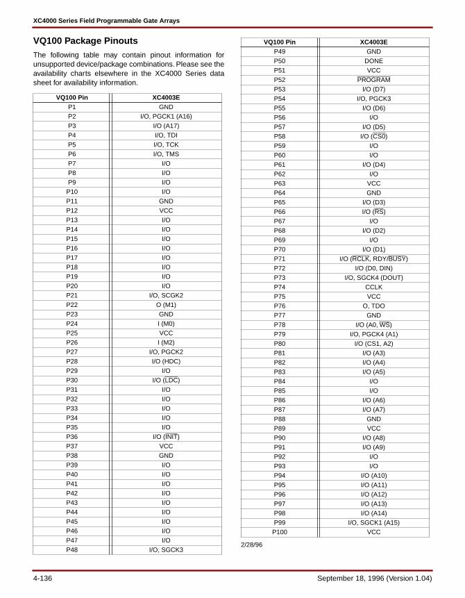
XC4000 Series Field Programmable Gate Arrays
VQ100 Package PinoutsThe following table may contain pinout information forunsupported device/package combinations. Please see theavailability charts elsewhere in the XC4000 Series datasheet for availability information.
2/28/96
VQ100 Pin XC4003EP1 GND
P2 I/O, PGCK1 (A16)
P3 I/O (A17)
P4 I/O, TDI
P5 I/O, TCK
P6 I/O, TMS
P7 I/O
P8 I/O
P9 I/O
P10 I/O
P11 GND
P12 VCC
P13 I/O
P14 I/O
P15 I/O
P16 I/O
P17 I/O
P18 I/O
P19 I/O
P20 I/O
P21 I/O, SCGK2
P22 O (M1)
P23 GND
P24 I (M0)
P25 VCC
P26 I (M2)
P27 I/O, PGCK2
P28 I/O (HDC)
P29 I/O
P30 I/O (LDC)
P31 I/O
P32 I/O
P33 I/O
P34 I/O
P35 I/O
P36 I/O (INIT)
P37 VCC
P38 GND
P39 I/O
P40 I/O
P41 I/O
P42 I/O
P43 I/O
P44 I/O
P45 I/O
P46 I/O
P47 I/O
P48 I/O, SGCK3
P49 GND
P50 DONE
P51 VCC
P52 PROGRAM
P53 I/O (D7)
P54 I/O, PGCK3
P55 I/O (D6)
P56 I/O
P57 I/O (D5)
P58 I/O (CS0)
P59 I/O
P60 I/O
P61 I/O (D4)
P62 I/O
P63 VCC
P64 GND
P65 I/O (D3)
P66 I/O (RS)
P67 I/O
P68 I/O (D2)
P69 I/O
P70 I/O (D1)
P71 I/O (RCLK, RDY/BUSY)
P72 I/O (D0, DIN)
P73 I/O, SGCK4 (DOUT)
P74 CCLK
P75 VCC
P76 O, TDO
P77 GND
P78 I/O (A0, WS)
P79 I/O, PGCK4 (A1)
P80 I/O (CS1, A2)
P81 I/O (A3)
P82 I/O (A4)
P83 I/O (A5)
P84 I/O
P85 I/O
P86 I/O (A6)
P87 I/O (A7)
P88 GND
P89 VCC
P90 I/O (A8)
P91 I/O (A9)
P92 I/O
P93 I/O
P94 I/O (A10)
P95 I/O (A11)
P96 I/O (A12)
P97 I/O (A13)
P98 I/O (A14)
P99 I/O, SGCK1 (A15)
P100 VCC
VQ100 Pin XC4003E
4-136 September 18, 1996 (Version 1.04)
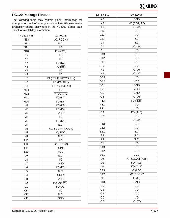
PG120 Package PinoutsThe following table may contain pinout information forunsupported device/package combinations. Please see theavailability charts elsewhere in the XC4000 Series datasheet for availability information.
PG120 Pin XC4003EN13 I/O, PGCK3N12 N.C.N11 I/ON10 I/O (CS0)N9 I/ON8 I/ON7 I/O (D3)N6 I/O (RS)N5 I/ON4 I/ON3 I/O (RCLK, RDY/BUSY)N2 I/O (D0, DIN)N1 I/O, PGCK4 (A1)
M13 I/OM12 PROGRAMM11 I/O (D7)M10 I/O (D6)M9 I/O (D5)M8 I/O (D4)M7 VCCM6 I/OM5 I/O (D1)M4 N.C.M3 I/O, SGCK4 (DOUT)M2 O, TDOM1 N.C.L13 I/OL12 I/O, SGCK3L11 DONEL10 VCCL9 N.C.L8 I/OL7 GNDL6 I/O (D2)L5 N.C.L4 CCLKL3 VCCL2 I/O (A0, WS)L1 I/O (A3)
K13 I/OK12 N.C.K11 GND
K3 GNDK2 I/O (CS1, A2)K1 I/O (A5)J13 I/OJ12 I/OJ11 N.C.J3 N.C.J2 I/O (A4)J1 I/O
H13 I/OH12 I/OH11 I/OH3 I/OH2 I/O (A6)H1 I/O (A7)
G13 I/OG12 VCCG11 GNDG3 VCCG2 GNDG1 I/O (A8)F13 I/O (INIT)F12 I/OF11 I/OF3 I/O (A10)F2 I/OF1 I/O (A9)
E13 I/OE12 I/OE11 N.C.E3 N.C.E2 N.C.E1 I/O
D13 I/OD12 I/OD11 VCCD3 I/O, SGCK1 (A15)D2 I/O (A13)D1 I/O (A11)C13 I/O (LDC)C12 I/O, PGCK2C11 I (M0)C10 GNDC9 I/OC8 I/OC7 VCCC6 I/OC5 I/O, TDI
PG120 Pin XC4003E
September 18, 1996 (Version 1.04) 4-137

XC4000 Series Field Programmable Gate Arrays
3/13/96
Note: Viewed from the bottom side, the package pins startat the top row and go from the left edge to the right edge.Viewed from the top side, the pins start at the top row andgo from the right edge to the left edge.
C4 GNDC3 VCCC2 I/O (A14)C1 I/O (A12)B13 N.C.B12 I (M2)B11 O (M1)B10 N.C.B9 I/OB8 I/OB7 GNDB6 I/OB5 I/O, TMSB4 I/O, TCKB3 I/O (A17)B2 I/O, PGCK1 (A16)B1 N.C.A13 I/O (HDC)
PG120 Pin XC4003EA12 I/O, SCGK2A11 I/OA10 I/OA9 I/OA8 I/OA7 I/OA6 I/OA5 I/OA4 I/OA3 N.C.A2 N.C.A1 N.C.
PG120 Pin XC4003E
4-138 September 18, 1996 (Version 1.04)

TQ144 Package PinoutsThe following table may contain pinout information forunsupported device/package combinations. Please see theavailability charts elsewhere in the XC4000 Series datasheet for availability information.
TQ144 Pin XC4005E XC4006EP1 GND GNDP2 I/O, PGCK1 (A16) I/O, PGCK1 (A16)P3 I/O (A17) I/O (A17)P4 I/O I/OP5 I/O I/OP6 I/O, TDI I/O, TDIP7 I/O, TCK I/O, TCKP8 GND GNDP9 I/O I/OP10 I/O I/OP11 I/O, TMS I/O, TMSP12 I/O I/OP13 I/O I/OP14 I/O I/OP15 I/O I/OP16 I/O I/OP17 GND GNDP18 VCC VCCP19 I/O I/OP20 I/O I/OP21 I/O I/OP22 I/O I/OP23 I/O I/OP24 I/O I/OP25 I/O I/OP26 I/O I/OP27 GND GNDP28 I/O I/OP29 I/O I/OP30 I/O I/OP31 I/O I/OP32 I/O I/OP33 I/O, SCGK2 I/O, SCGK2P34 O (M1) O (M1)P35 GND GNDP36 I (M0) I (M0)P37 VCC VCCP38 I (M2) I (M2)P39 I/O, PGCK2 I/O, PGCK2P40 I/O (HDC) I/O (HDC)P41 I/O I/OP42 I/O I/O
P43 I/O I/OP44 I/O (LDC) I/O (LDC)P45 GND GNDP46 I/O I/OP47 I/O I/OP48 I/O I/OP49 I/O I/OP50 I/O I/OP51 I/O I/OP52 I/O I/OP53 I/O (INIT) I/O (INIT)P54 VCC VCCP55 GND GNDP56 I/O I/OP57 I/O I/OP58 I/O I/OP59 I/O I/OP60 I/O I/OP61 I/O I/OP62 I/O I/OP63 I/O I/OP64 GND GNDP65 I/O I/OP66 I/O I/OP67 I/O I/OP68 I/O I/OP69 I/O I/OP70 I/O, SGCK3 I/O, SGCK3P71 GND GNDP72 DONE DONEP73 VCC VCCP74 PROGRAM PROGRAMP75 I/O (D7) I/O (D7)P76 I/O, PGCK3 I/O, PGCK3P77 I/O I/OP78 I/O I/OP79 I/O (D6) I/O (D6)P80 I/O I/OP81 GND GNDP82 I/O I/OP83 I/O I/OP84 I/O (D5) I/O (D5)P85 I/O (CS0) I/O (CS0)P86 I/O I/OP87 I/O I/OP88 I/O (D4) I/O (D4)P89 I/O I/OP90 VCC VCC
TQ144 Pin XC4005E XC4006E
September 18, 1996 (Version 1.04) 4-139

XC4000 Series Field Programmable Gate Arrays
2/28/96
Note: Shaded pins should be taken into account whendesigning PC boards, in case of future replacement by dif-ferent devices.
P91 GND GNDP92 I/O (D3) I/O (D3)P93 I/O (RS) I/O (RS)P94 I/O I/OP95 I/O I/OP96 I/O (D2) I/O (D2)P97 I/O I/OP98 I/O I/OP99 I/O I/OP100 GND GNDP101 I/O (D1) I/O (D1)P102 I/O (RCLK,
RDY/BUSY)I/O (RCLK, RDY/BUSY)
P103 I/O I/OP104 I/O I/OP105 I/O (D0, DIN) I/O (D0, DIN)P106 I/O, SGCK4 (DOUT) I/O, SGCK4 (DOUT)P107 CCLK CCLKP108 VCC VCCP109 O, TDO O, TDOP110 GND GNDP111 I/O (A0, WS) I/O (A0, WS)P112 I/O, PGCK4 (A1) I/O, PGCK4 (A1)P113 I/O I/OP114 I/O I/OP115 I/O (CS1, A2) I/O (CS1, A2)P116 I/O (A3) I/O (A3)P117 N.C. I/OP118 GND GNDP119 I/O I/O
TQ144 Pin XC4005E XC4006EP120 I/O I/OP121 I/O (A4) I/O (A4)P122 I/O (A5) I/O (A5)P123 I/O I/OP124 I/O I/OP125 I/O (A6) I/O (A6)P126 I/O (A7) I/O (A7)P127 GND GNDP128 VCC VCCP129 I/O (A8) I/O (A8)P130 I/O (A9) I/O (A9)P131 I/O I/OP132 I/O I/OP133 I/O (A10) I/O (A10)P134 I/O (A11) I/O (A11)P135 I/O I/OP136 I/O I/OP137 GND GNDP138 I/O (A12) I/O (A12)P139 I/O (A13) I/O (A13)P140 I/O I/OP141 I/O I/OP142 I/O (A14) I/O (A14)P143 I/O, SGCK1 (A15) I/O, SGCK1 (A15)P144 VCC VCC
TQ144 Pin XC4005E XC4006E
4-140 September 18, 1996 (Version 1.04)

PG156 Package PinoutsThe following table may contain pinout information forunsupported device/package combinations. Please see theavailability charts elsewhere in the XC4000 Series datasheet for availability information.
PG156 Pin XC4005E XC4006ET1 O, TDO O, TDOT2 I/O, SGCK4 (DOUT) I/O, SGCK4 (DOUT)T3 I/O (D1) I/O (D1)T4 I/O I/OT5 I/O I/OT6 I/O I/OT7 I/O (RS) I/O (RS)T8 I/O (D3) I/O (D3)T9 I/O I/OT10 I/O (D5) I/O (D5)T11 I/O I/OT12 N.C. I/OT13 I/O I/OT14 I/O (D6) I/O (D6)T15 I/O, PGCK3 I/O, PGCK3T16 I/O (D7) I/O (D7)R1 I/O (A0, WS) I/O (A0, WS)R2 CCLK CCLKR3 I/O I/OR4 I/O I/OR5 N.C. I/OR6 I/O I/OR7 I/O I/OR8 VCC VCCR9 I/O (D4) I/O (D4)R10 I/O I/OR11 I/O I/OR12 N.C. I/OR13 I/O I/OR14 PROGRAM PROGRAMR15 DONE DONER16 I/O, SGCK3 I/O, SGCK3P1 I/O (CS1, A2) I/O (CS1, A2)P2 I/O, PGCK4 (A1) I/O, PGCK4 (A1)P3 VCC VCCP4 I/O (D0, DIN) I/O (D0, DIN)P5 I/O (RCLK,
RDY/BUSY)I/O (RCLK, RDY/BUSY)
P6 GND GNDP7 I/O (D2) I/O (D2)P8 GND GNDP9 I/O I/OP10 I/O (CS0) I/O (CS0)
P11 GND GNDP12 I/O I/OP13 VCC VCCP14 GND GNDP15 I/O I/OP16 I/O I/ON1 I/O (A3) I/O (A3)N2 I/O I/ON3 GND GNDN14 I/O I/ON15 I/O I/ON16 N.C. I/OM1 N.C. I/OM2 N.C. I/OM3 I/O I/OM14 I/O I/OM15 N.C. I/OM16 I/O I/OL1 I/O I/OL2 I/O I/OL3 GND GNDL14 GND GNDL15 I/O I/OL16 I/O I/OK1 I/O I/OK2 I/O (A5) I/O (A5)K3 I/O (A4) I/O (A4)K14 I/O I/OK15 I/O I/OK16 I/O I/OJ1 I/O I/OJ2 I/O (A6) I/O (A6)J3 I/O (A7) I/O (A7)J14 GND GNDJ15 I/O I/OJ16 I/O I/OH1 I/O (A8) I/O (A8)H2 GND GNDH3 VCC VCCH14 VCC VCCH15 I/O (INIT) I/O (INIT)H16 I/O I/OG1 I/O (A9) I/O (A9)G2 I/O I/OG3 I/O I/OG14 I/O I/OG15 I/O I/OG16 I/O I/O
PG156 Pin XC4005E XC4006E
September 18, 1996 (Version 1.04) 4-141

XC4000 Series Field Programmable Gate Arrays
2/28/96
Note: Shaded pins should be taken into account whendesigning PC boards, in case of future replacement by dif-ferent devices.
Note: Viewed from the bottom side, the package pins startat the top row and go from the left edge to the right edge.Viewed from the top side, the pins start at the top row andgo from the right edge to the left edge.
F1 I/O (A10) I/O (A10)F2 I/O (A11) I/O (A11)F3 GND GNDF14 GND GNDF15 I/O I/OF16 I/O I/OE1 I/O I/OE2 I/O I/OE3 I/O (A12) I/O (A12)E14 I/O I/OE15 N.C. I/OE16 I/O I/OD1 N.C. I/OD2 N.C. I/OD3 I/O I/OD14 I/O (HDC) I/O (HDC)D15 I/O I/OD16 N.C. I/OC1 I/O (A13) I/O (A13)C2 I/O I/OC3 VCC VCCC4 GND GNDC5 I/O I/OC6 GND GNDC7 I/O I/OC8 GND GNDC9 I/O I/OC10 I/O I/OC11 GND GNDC12 I/O I/OC13 GND GNDC14 VCC VCCC15 I/O I/OC16 I/O (LDC) I/O (LDC)B1 I/O (A14) I/O (A14)B2 I/O, SGCK1 (A15) I/O, SGCK1 (A15)B3 I/O, PGCK1 (A16) I/O, PGCK1 (A16)B4 I/O, TDI I/O, TDI
PG156 Pin XC4005E XC4006EB5 I/O I/OB6 I/O I/OB7 I/O I/OB8 VCC VCCB9 I/O I/OB10 I/O I/OB11 I/O I/OB12 I/O I/OB13 I/O I/OB14 I/O, SCGK2 I/O, SCGK2B15 I (M2) I (M2)B16 I/O, PGCK2 I/O, PGCK2A1 I/O (A17) I/O (A17)A2 I/O I/OA3 I/O, TCK I/O, TCKA4 N.C. I/OA5 I/O, TMS I/O, TMSA6 I/O I/OA7 I/O I/OA8 I/O I/OA9 I/O I/OA10 I/O I/OA11 I/O I/OA12 N.C. I/OA13 I/O I/OA14 I/O I/OA15 O (M1) O (M1)A16 I (M0) I (M0)
PG156 Pin XC4005E XC4006E
4-142 September 18, 1996 (Version 1.04)
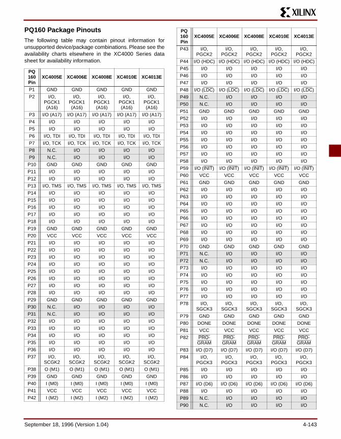
PQ160 Package PinoutsThe following table may contain pinout information forunsupported device/package combinations. Please see theavailability charts elsewhere in the XC4000 Series datasheet for availability information.
PQ160Pin
XC4005E XC4006E XC4008E XC4010E XC4013E
P1 GND GND GND GND GND
P2 I/O, PGCK1 (A16)
I/O, PGCK1 (A16)
I/O, PGCK1 (A16)
I/O, PGCK1 (A16)
I/O, PGCK1 (A16)
P3 I/O (A17) I/O (A17) I/O (A17) I/O (A17) I/O (A17)
P4 I/O I/O I/O I/O I/O
P5 I/O I/O I/O I/O I/O
P6 I/O, TDI I/O, TDI I/O, TDI I/O, TDI I/O, TDI
P7 I/O, TCK I/O, TCK I/O, TCK I/O, TCK I/O, TCK
P8 N.C. I/O I/O I/O I/O
P9 N.C. I/O I/O I/O I/O
P10 GND GND GND GND GND
P11 I/O I/O I/O I/O I/O
P12 I/O I/O I/O I/O I/O
P13 I/O, TMS I/O, TMS I/O, TMS I/O, TMS I/O, TMS
P14 I/O I/O I/O I/O I/O
P15 I/O I/O I/O I/O I/O
P16 I/O I/O I/O I/O I/O
P17 I/O I/O I/O I/O I/O
P18 I/O I/O I/O I/O I/O
P19 GND GND GND GND GND
P20 VCC VCC VCC VCC VCC
P21 I/O I/O I/O I/O I/O
P22 I/O I/O I/O I/O I/O
P23 I/O I/O I/O I/O I/O
P24 I/O I/O I/O I/O I/O
P25 I/O I/O I/O I/O I/O
P26 I/O I/O I/O I/O I/O
P27 I/O I/O I/O I/O I/O
P28 I/O I/O I/O I/O I/O
P29 GND GND GND GND GND
P30 N.C. I/O I/O I/O I/O
P31 N.C. I/O I/O I/O I/O
P32 I/O I/O I/O I/O I/O
P33 I/O I/O I/O I/O I/O
P34 I/O I/O I/O I/O I/O
P35 I/O I/O I/O I/O I/O
P36 I/O I/O I/O I/O I/O
P37 I/O, SCGK2
I/O, SCGK2
I/O, SCGK2
I/O, SCGK2
I/O, SCGK2
P38 O (M1) O (M1) O (M1) O (M1) O (M1)
P39 GND GND GND GND GND
P40 I (M0) I (M0) I (M0) I (M0) I (M0)
P41 VCC VCC VCC VCC VCC
P42 I (M2) I (M2) I (M2) I (M2) I (M2)
P43 I/O, PGCK2
I/O, PGCK2
I/O, PGCK2
I/O, PGCK2
I/O, PGCK2
P44 I/O (HDC) I/O (HDC) I/O (HDC) I/O (HDC) I/O (HDC)
P45 I/O I/O I/O I/O I/O
P46 I/O I/O I/O I/O I/O
P47 I/O I/O I/O I/O I/O
P48 I/O (LDC) I/O (LDC) I/O (LDC) I/O (LDC) I/O (LDC)
P49 N.C. I/O I/O I/O I/O
P50 N.C. I/O I/O I/O I/O
P51 GND GND GND GND GND
P52 I/O I/O I/O I/O I/O
P53 I/O I/O I/O I/O I/O
P54 I/O I/O I/O I/O I/O
P55 I/O I/O I/O I/O I/O
P56 I/O I/O I/O I/O I/O
P57 I/O I/O I/O I/O I/O
P58 I/O I/O I/O I/O I/O
P59 I/O (INIT) I/O (INIT) I/O (INIT) I/O (INIT) I/O (INIT)
P60 VCC VCC VCC VCC VCC
P61 GND GND GND GND GND
P62 I/O I/O I/O I/O I/O
P63 I/O I/O I/O I/O I/O
P64 I/O I/O I/O I/O I/O
P65 I/O I/O I/O I/O I/O
P66 I/O I/O I/O I/O I/O
P67 I/O I/O I/O I/O I/O
P68 I/O I/O I/O I/O I/O
P69 I/O I/O I/O I/O I/O
P70 GND GND GND GND GND
P71 N.C. I/O I/O I/O I/O
P72 N.C. I/O I/O I/O I/O
P73 I/O I/O I/O I/O I/O
P74 I/O I/O I/O I/O I/O
P75 I/O I/O I/O I/O I/O
P76 I/O I/O I/O I/O I/O
P77 I/O I/O I/O I/O I/O
P78 I/O, SGCK3
I/O, SGCK3
I/O, SGCK3
I/O, SGCK3
I/O, SGCK3
P79 GND GND GND GND GND
P80 DONE DONE DONE DONE DONE
P81 VCC VCC VCC VCC VCC
P82 PRO-GRAM
PRO-GRAM
PRO-GRAM
PRO-GRAM
PRO-GRAM
P83 I/O (D7) I/O (D7) I/O (D7) I/O (D7) I/O (D7)
P84 I/O, PGCK3
I/O, PGCK3
I/O, PGCK3
I/O, PGCK3
I/O, PGCK3
P85 I/O I/O I/O I/O I/O
P86 I/O I/O I/O I/O I/O
P87 I/O (D6) I/O (D6) I/O (D6) I/O (D6) I/O (D6)
P88 I/O I/O I/O I/O I/O
P89 N.C. I/O I/O I/O I/O
P90 N.C. I/O I/O I/O I/O
PQ160Pin
XC4005E XC4006E XC4008E XC4010E XC4013E
September 18, 1996 (Version 1.04) 4-143

XC4000 Series Field Programmable Gate Arrays
2/28/96
Note: Shaded pins should be taken into account whendesigning PC boards, in case of future replacement by dif-ferent devices.
P91 GND GND GND GND GND
P92 I/O I/O I/O I/O I/O
P93 I/O I/O I/O I/O I/O
P94 I/O (D5) I/O (D5) I/O (D5) I/O (D5) I/O (D5)
P95 I/O (CS0) I/O (CS0) I/O (CS0) I/O (CS0) I/O (CS0)
P96 I/O I/O I/O I/O I/O
P97 I/O I/O I/O I/O I/O
P98 I/O (D4) I/O (D4) I/O (D4) I/O (D4) I/O (D4)
P99 I/O I/O I/O I/O I/O
P100 VCC VCC VCC VCC VCC
P101 GND GND GND GND GND
P102 I/O (D3) I/O (D3) I/O (D3) I/O (D3) I/O (D3)
P103 I/O (RS) I/O (RS) I/O (RS) I/O (RS) I/O (RS)
P104 I/O I/O I/O I/O I/O
P105 I/O I/O I/O I/O I/O
P106 I/O (D2) I/O (D2) I/O (D2) I/O (D2) I/O (D2)
P107 I/O I/O I/O I/O I/O
P108 I/O I/O I/O I/O I/O
P109 I/O I/O I/O I/O I/O
P110 GND GND GND GND GND
P111 N.C. I/O I/O I/O I/O
P112 N.C. I/O I/O I/O I/O
P113 I/O (D1) I/O (D1) I/O (D1) I/O (D1) I/O (D1)
P114 I/O (RCLK, RDY/
BUSY)
I/O (RCLK, RDY/
BUSY)
I/O (RCLK, RDY/
BUSY)
I/O (RCLK, RDY/
BUSY)
I/O (RCLK, RDY/
BUSY)
P115 I/O I/O I/O I/O I/O
P116 I/O I/O I/O I/O I/O
P117 I/O (D0, DIN)
I/O (D0, DIN)
I/O (D0, DIN)
I/O (D0, DIN)
I/O (D0, DIN)
P118 I/O, SGCK4 (DOUT)
I/O, SGCK4 (DOUT)
I/O, SGCK4 (DOUT)
I/O, SGCK4 (DOUT)
I/O, SGCK4 (DOUT)
P119 CCLK CCLK CCLK CCLK CCLK
P120 VCC VCC VCC VCC VCC
P121 O, TDO O, TDO O, TDO O, TDO O, TDO
P122 GND GND GND GND GND
P123 I/O (A0, WS)
I/O (A0, WS)
I/O (A0, WS)
I/O (A0, WS)
I/O (A0, WS)
P124 I/O, PGCK4
(A1)
I/O, PGCK4
(A1)
I/O, PGCK4
(A1)
I/O, PGCK4
(A1)
I/O, PGCK4
(A1)
P125 I/O I/O I/O I/O I/O
P126 I/O I/O I/O I/O I/O
PQ160Pin
XC4005E XC4006E XC4008E XC4010E XC4013E
P127 I/O (CS1, A2)
I/O (CS1, A2)
I/O (CS1, A2)
I/O (CS1, A2)
I/O (CS1, A2)
P128 I/O (A3) I/O (A3) I/O (A3) I/O (A3) I/O (A3)
P129 N.C. I/O I/O I/O I/O
P130 N.C. I/O I/O I/O I/O
P131 GND GND GND GND GND
P132 I/O I/O I/O I/O I/O
P133 I/O I/O I/O I/O I/O
P134 I/O (A4) I/O (A4) I/O (A4) I/O (A4) I/O (A4)
P135 I/O (A5) I/O (A5) I/O (A5) I/O (A5) I/O (A5)
P136 N.C. N.C. I/O I/O I/O
P137 I/O I/O I/O I/O I/O
P138 I/O I/O I/O I/O I/O
P139 I/O (A6) I/O (A6) I/O (A6) I/O (A6) I/O (A6)
P140 I/O (A7) I/O (A7) I/O (A7) I/O (A7) I/O (A7)
P141 GND GND GND GND GND
P142 VCC VCC VCC VCC VCC
P143 I/O (A8) I/O (A8) I/O (A8) I/O (A8) I/O (A8)
P144 I/O (A9) I/O (A9) I/O (A9) I/O (A9) I/O (A9)
P145 I/O I/O I/O I/O I/O
P146 I/O I/O I/O I/O I/O
P147 I/O (A10) I/O (A10) I/O (A10) I/O (A10) I/O (A10)
P148 I/O (A11) I/O (A11) I/O (A11) I/O (A11) I/O (A11)
P149 I/O I/O I/O I/O I/O
P150 I/O I/O I/O I/O I/O
P151 GND GND GND GND GND
P152 N.C. I/O I/O I/O I/O
P153 N.C. I/O I/O I/O I/O
P154 I/O (A12) I/O (A12) I/O (A12) I/O (A12) I/O (A12)
P155 I/O (A13) I/O (A13) I/O (A13) I/O (A13) I/O (A13)
P156 I/O I/O I/O I/O I/O
P157 I/O I/O I/O I/O I/O
P158 I/O (A14) I/O (A14) I/O (A14) I/O (A14) I/O (A14)
P159 I/O, SGCK1 (A15)
I/O, SGCK1 (A15)
I/O, SGCK1 (A15)
I/O, SGCK1 (A15)
I/O, SGCK1 (A15)
P160 VCC VCC VCC VCC VCC
PQ160Pin
XC4005E XC4006E XC4008E XC4010E XC4013E
4-144 September 18, 1996 (Version 1.04)

TQ176 Package PinoutsThe following table may contain pinout information forunsupported device/package combinations. Please see theavailability charts elsewhere in the XC4000 Series datasheet for availability information.
TQ176 Pin XC4010LP1 GNDP2 I/O, PGCK1 (A16)P3 I/O (A17)P4 I/OP5 I/OP6 I/O, TDIP7 I/O, TCKP8 I/OP9 I/OP10 GNDP11 I/OP12 I/OP13 I/O, TMSP14 I/OP15 I/OP16 I/OP17 I/OP18 I/OP19 I/OP20 I/OP21 GNDP22 VCCP23 I/OP24 I/OP25 I/OP26 I/OP27 I/OP28 I/OP29 I/OP30 I/OP31 I/OP32 I/OP33 GNDP34 I/OP35 I/OP36 I/OP37 I/OP38 I/OP39 I/OP40 I/OP41 I/O, SCGK2P42 O (M1)
P43 GNDP44 I (M0)P45 VCCP46 I (M2)P47 I/O, PGCK2P48 I/O (HDC)P49 I/OP50 I/OP51 I/OP52 I/O (LDC)P53 I/OP54 I/OP55 GNDP56 I/OP57 I/OP58 I/OP59 I/OP60 I/OP61 I/OP62 I/OP63 I/OP64 I/OP65 I/O (INIT)P66 VCCP67 GNDP68 I/OP69 I/OP70 I/OP71 I/OP72 I/OP73 I/OP74 I/OP75 I/OP76 I/OP77 I/OP78 GNDP79 I/OP80 I/OP81 I/OP82 I/OP83 I/OP84 I/OP85 I/OP86 I/O, SGCK3P87 GNDP88 DONEP89 VCCP90 PROGRAM
TQ176 Pin XC4010L
September 18, 1996 (Version 1.04) 4-145

XC4000 Series Field Programmable Gate Arrays
3/15/96
PG191 Package Pinouts (see PG223)The PG191 package pinout has been combined with the PG223 in a single table, because of their physical compat-ibility. The PG191 has the same dimensions as the PG223, but has 32 fewer pins on the inner ring.
P91 I/O (D7)P92 I/O, PGCK3P93 I/OP94 I/OP95 I/O (D6)P96 I/OP97 I/OP98 I/OP99 GNDP100 I/OP101 I/OP102 I/O (D5)P103 I/O (CS0)P104 I/OP105 I/OP106 I/OP107 I/OP108 I/O (D4)P109 I/OP110 VCCP111 GNDP112 I/O (D3)P113 I/O (RS)P114 I/OP115 I/OP116 I/OP117 I/OP118 I/O (D2)P119 I/OP120 I/OP121 I/OP122 GNDP123 I/OP124 I/OP125 I/O (D1)P126 I/O (RCLK, RDY/BUSY)P127 I/OP128 I/OP129 I/O (D0, DIN)P130 I/O, SGCK4 (DOUT)P131 CCLKP132 VCCP133 O, TDOP134 GNDP135 I/O (A0, WS)P136 I/O, PGCK4 (A1)P137 I/OP138 I/O
TQ176 Pin XC4010LP139 I/O (CS1, A2)P140 I/O (A3)P141 I/OP142 I/OP143 GNDP144 I/OP145 I/OP146 I/O (A4)P147 I/O (A5)P148 I/OP149 I/OP150 I/OP151 I/OP152 I/O (A6)P153 I/O (A7)P154 GNDP155 VCCP156 I/O (A8)P157 I/O (A9)P158 I/OP159 I/OP160 I/OP161 I/OP162 I/O (A10)P163 I/O (A11)P164 I/OP165 I/OP166 GNDP167 I/OP168 I/OP169 I/OP170 I/O (A12)P171 I/O (A13)P172 I/OP173 I/OP174 I/O (A14)P175 I/O, SGCK1 (A15)P176 VCC
TQ176 Pin XC4010L
4-146 September 18, 1996 (Version 1.04)

PQ208, HQ208 Package PinoutsThe following table may contain pinout information forunsupported device/package combinations. Please see theavailability charts elsewhere in the XC4000 Series datasheet for availability information.
PQ208 Pin
XC4005E/L
XC4006
E
XC4008
E
XC4010E/L
XC4013E/L
XC4020
E
XC4028
EX/XL
P1 N.C. N.C. N.C. N.C. N.C. N.C. N.C.
P2 GND GND GND GND GND GND GND
P3 N.C. N.C. N.C. N.C. N.C. N.C. N.C.
P4 I/O, PGCK1 (A16)
I/O, PGCK1 (A16)
I/O, PGCK1 (A16)
I/O, PGCK1 (A16)
I/O, PGCK1 (A16)
I/O, PGCK1 (A16)
I/O, GCK1 (A16)
P5 I/O (A17)
I/O (A17)
I/O (A17)
I/O (A17)
I/O (A17)
I/O (A17)
I/O (A17)
P6 I/O I/O I/O I/O I/O I/O I/O
P7 I/O I/O I/O I/O I/O I/O I/O
P8 I/O, TDI I/O, TDI I/O, TDI I/O, TDI I/O, TDI I/O, TDI I/O, TDI
P9 I/O, TCK
I/O, TCK
I/O, TCK
I/O, TCK
I/O, TCK
I/O, TCK
I/O, TCK
P10 N.C. I/O I/O I/O I/O I/O I/O
P11 N.C. I/O I/O I/O I/O I/O I/O
P12 N.C. N.C. N.C. I/O I/O I/O I/O
P13 N.C. N.C. N.C. I/O I/O I/O I/O
P14 GND GND GND GND GND GND GND
P15 I/O I/O I/O I/O I/O I/O I/O, FCLK1
P16 I/O I/O I/O I/O I/O I/O I/O
P17 I/O, TMS
I/O, TMS
I/O, TMS
I/O, TMS
I/O, TMS
I/O, TMS
I/O, TMS
P18 I/O I/O I/O I/O I/O I/O I/O
P19 N.C. N.C. I/O I/O I/O I/O I/O
P20 N.C. N.C. I/O I/O I/O I/O I/O
P21 I/O I/O I/O I/O I/O I/O I/O
P22 I/O I/O I/O I/O I/O I/O I/O
P23 I/O I/O I/O I/O I/O I/O I/O
P24 I/O I/O I/O I/O I/O I/O I/O
P25 GND GND GND GND GND GND GND
P26 VCC VCC VCC VCC VCC VCC VCC
P27 I/O I/O I/O I/O I/O I/O I/O
P28 I/O I/O I/O I/O I/O I/O I/O
P29 I/O I/O I/O I/O I/O I/O I/O
P30 I/O I/O I/O I/O I/O I/O I/O
P31 N.C. N.C. I/O I/O I/O I/O I/O
P32 N.C. N.C. I/O I/O I/O I/O I/O
P33 I/O I/O I/O I/O I/O I/O I/O
P34 I/O I/O I/O I/O I/O I/O I/O
P35 I/O I/O I/O I/O I/O I/O I/O
P36 I/O I/O I/O I/O I/O I/O I/O, FCLK2
P37 GND GND GND GND GND GND GND
P38 N.C. N.C. N.C. I/O I/O I/O I/O
P39 N.C. N.C. N.C. I/O I/O I/O I/O
P40 N.C. I/O I/O I/O I/O I/O I/O
P41 N.C. I/O I/O I/O I/O I/O I/O
P42 I/O I/O I/O I/O I/O I/O I/O
P43 I/O I/O I/O I/O I/O I/O I/O
P44 I/O I/O I/O I/O I/O I/O I/O
P45 I/O I/O I/O I/O I/O I/O I/O
P46 I/O I/O I/O I/O I/O I/O I/O
P47 I/O, SGCK2
I/O, SGCK2
I/O, SGCK2
I/O, SGCK2
I/O, SGCK2
I/O, SGCK2
I/O, GCK2
P48 O (M1) O (M1) O (M1) O (M1) O (M1) O (M1) O (M1)
P49 GND GND GND GND GND GND GND
P50 I (M0) I (M0) I (M0) I (M0) I (M0) I (M0) I (M0)
P51 N.C. N.C. N.C. N.C. N.C. N.C. N.C.
P52 N.C. N.C. N.C. N.C. N.C. N.C. N.C.
P53 N.C. N.C. N.C. N.C. N.C. N.C. N.C.
P54 N.C. N.C. N.C. N.C. N.C. N.C. N.C.
P55 VCC VCC VCC VCC VCC VCC VCC
P56 I (M2) I (M2) I (M2) I (M2) I (M2) I (M2) I (M2)
P57 I/O, PGCK2
I/O, PGCK2
I/O, PGCK2
I/O, PGCK2
I/O, PGCK2
I/O, PGCK2
I/O, GCK3
P58 I/O (HDC)
I/O (HDC)
I/O (HDC)
I/O (HDC)
I/O (HDC)
I/O (HDC)
I/O (HDC)
P59 I/O I/O I/O I/O I/O I/O I/O
P60 I/O I/O I/O I/O I/O I/O I/O
P61 I/O I/O I/O I/O I/O I/O I/O
P62 I/O (LDC)
I/O (LDC)
I/O (LDC)
I/O (LDC)
I/O (LDC)
I/O (LDC)
I/O (LDC)
P63 N.C. I/O I/O I/O I/O I/O I/O
P64 N.C. I/O I/O I/O I/O I/O I/O
P65 N.C. N.C. N.C. I/O I/O I/O I/O
P66 N.C. N.C. N.C. I/O I/O I/O I/O
P67 GND GND GND GND GND GND GND
P68 I/O I/O I/O I/O I/O I/O I/O
P69 I/O I/O I/O I/O I/O I/O I/O
P70 I/O I/O I/O I/O I/O I/O I/O
P71 I/O I/O I/O I/O I/O I/O I/O
P72 N.C. N.C. I/O I/O I/O I/O I/O
P73 N.C. N.C. I/O I/O I/O I/O I/O
P74 I/O I/O I/O I/O I/O I/O I/O
P75 I/O I/O I/O I/O I/O I/O I/O
P76 I/O I/O I/O I/O I/O I/O I/O
P77 I/O (INIT)
I/O (INIT)
I/O (INIT)
I/O (INIT)
I/O (INIT)
I/O (INIT)
I/O (INIT)
P78 VCC VCC VCC VCC VCC VCC VCC
P79 GND GND GND GND GND GND GND
P80 I/O I/O I/O I/O I/O I/O I/O
P81 I/O I/O I/O I/O I/O I/O I/O
P82 I/O I/O I/O I/O I/O I/O I/O
P83 I/O I/O I/O I/O I/O I/O I/O
P84 N.C. N.C. I/O I/O I/O I/O I/O
P85 N.C. N.C. I/O I/O I/O I/O I/O
P86 I/O I/O I/O I/O I/O I/O I/O
P87 I/O I/O I/O I/O I/O I/O I/O
PQ208 Pin
XC4005E/L
XC4006
E
XC4008
E
XC4010E/L
XC4013E/L
XC4020
E
XC4028
EX/XL
September 18, 1996 (Version 1.04) 4-147

XC4000 Series Field Programmable Gate Arrays
P88 I/O I/O I/O I/O I/O I/O I/O
P89 I/O I/O I/O I/O I/O I/O I/O
P90 GND GND GND GND GND GND GND
P91 N.C. N.C. N.C. I/O I/O I/O I/O
P92 N.C. N.C. N.C. I/O I/O I/O I/O
P93 N.C. I/O I/O I/O I/O I/O I/O
P94 N.C. I/O I/O I/O I/O I/O I/O
P95 I/O I/O I/O I/O I/O I/O I/O
P96 I/O I/O I/O I/O I/O I/O I/O
P97 I/O I/O I/O I/O I/O I/O I/O
P98 I/O I/O I/O I/O I/O I/O I/O
P99 I/O I/O I/O I/O I/O I/O I/O
P100 I/O, SGCK3
I/O, SGCK3
I/O, SGCK3
I/O, SGCK3
I/O, SGCK3
I/O, SGCK3
I/O, GCK4
P101 GND GND GND GND GND GND GND
P102 N.C. N.C. N.C. N.C. N.C. N.C. N.C.
P103 DONE DONE DONE DONE DONE DONE DONE
P104 N.C. N.C. N.C. N.C. N.C. N.C. N.C.
P105 N.C. N.C. N.C. N.C. N.C. N.C. N.C.
P106 VCC VCC VCC VCC VCC VCC VCC
P107 N.C. N.C. N.C. N.C. N.C. N.C. N.C.
P108 PRO-GRAM
PRO-GRAM
PRO-GRAM
PRO-GRAM
PRO-GRAM
PRO-GRAM
PRO-GRAM
P109 I/O (D7) I/O (D7) I/O (D7) I/O (D7) I/O (D7) I/O (D7) I/O (D7)
P110 I/O, PGCK3
I/O, PGCK3
I/O, PGCK3
I/O, PGCK3
I/O, PGCK3
I/O, PGCK3
I/O, GCK5
P111 I/O I/O I/O I/O I/O I/O I/O
P112 I/O I/O I/O I/O I/O I/O I/O
P113 I/O (D6) I/O (D6) I/O (D6) I/O (D6) I/O (D6) I/O (D6) I/O (D6)
P114 I/O I/O I/O I/O I/O I/O I/O
P115 N.C. I/O I/O I/O I/O I/O I/O
P116 N.C. I/O I/O I/O I/O I/O I/O
P117 N.C. N.C. N.C. I/O I/O I/O I/O
P118 N.C. N.C. N.C. I/O I/O I/O I/O
P119 GND GND GND GND GND GND GND
P120 I/O I/O I/O I/O I/O I/O I/O, FCLK3
P121 I/O I/O I/O I/O I/O I/O I/O
P122 I/O (D5) I/O (D5) I/O (D5) I/O (D5) I/O (D5) I/O (D5) I/O (D5)
P123 I/O (CS0)
I/O (CS0)
I/O (CS0)
I/O (CS0)
I/O (CS0)
I/O (CS0)
I/O (CS0)
P124 N.C. N.C. I/O I/O I/O I/O I/O
P125 N.C. N.C. I/O I/O I/O I/O I/O
P126 I/O I/O I/O I/O I/O I/O I/O
P127 I/O I/O I/O I/O I/O I/O I/O
P128 I/O (D4) I/O (D4) I/O (D4) I/O (D4) I/O (D4) I/O (D4) I/O (D4)
P129 I/O I/O I/O I/O I/O I/O I/O
P130 VCC VCC VCC VCC VCC VCC VCC
P131 GND GND GND GND GND GND GND
P132 I/O (D3) I/O (D3) I/O (D3) I/O (D3) I/O (D3) I/O (D3) I/O (D3)
P133 I/O (RS)
I/O (RS)
I/O (RS)
I/O (RS)
I/O (RS)
I/O (RS)
I/O (RS)
PQ208 Pin
XC4005E/L
XC4006
E
XC4008
E
XC4010E/L
XC4013E/L
XC4020
E
XC4028
EX/XL
P134 I/O I/O I/O I/O I/O I/O I/O
P135 I/O I/O I/O I/O I/O I/O I/O
P136 N.C. N.C. I/O I/O I/O I/O I/O
P137 N.C. N.C. I/O I/O I/O I/O I/O
P138 I/O (D2) I/O (D2) I/O (D2) I/O (D2) I/O (D2) I/O (D2) I/O (D2)
P139 I/O I/O I/O I/O I/O I/O I/O
P140 I/O I/O I/O I/O I/O I/O I/O
P141 I/O I/O I/O I/O I/O I/O I/O, FCLK4
P142 GND GND GND GND GND GND GND
P143 N.C. N.C. N.C. I/O I/O I/O I/O
P144 N.C. N.C. N.C. I/O I/O I/O I/O
P145 N.C. I/O I/O I/O I/O I/O I/O
P146 N.C. I/O I/O I/O I/O I/O I/O
P147 I/O (D1) I/O (D1) I/O (D1) I/O (D1) I/O (D1) I/O (D1) I/O (D1)
P148 I/O (RCLK, RDY/
BUSY)
I/O (RCLK, RDY/
BUSY)
I/O (RCLK, RDY/
BUSY)
I/O (RCLK, RDY/
BUSY)
I/O (RCLK, RDY/
BUSY)
I/O (RCLK, RDY/
BUSY)
I/O (RCLK, RDY/
BUSY)
P149 I/O I/O I/O I/O I/O I/O I/O
P150 I/O I/O I/O I/O I/O I/O I/O
P151 I/O (D0, DIN)
I/O (D0, DIN)
I/O (D0, DIN)
I/O (D0, DIN)
I/O (D0, DIN)
I/O (D0, DIN)
I/O (D0, DIN)
P152 I/O, SGCK
(DOUT)
I/O, SGCK4(DOUT)
I/O, SGCK4(DOUT)
I/O, SGCK4(DOUT)
I/O, SGCK4(DOUT)
I/O, SGCK4(DOUT)
I/O, GCK6
(DOUT)
P153 CCLK CCLK CCLK CCLK CCLK CCLK CCLK
P154 VCC VCC VCC VCC VCC VCC VCC
P155 N.C. N.C. N.C. N.C. N.C. N.C. N.C.
P156 N.C. N.C. N.C. N.C. N.C. N.C. N.C.
P157 N.C. N.C. N.C. N.C. N.C. N.C. N.C.
P158 N.C. N.C. N.C. N.C. N.C. N.C. N.C.
P159 O, TDO O, TDO O, TDO O, TDO O, TDO O, TDO O, TDO
P160 GND GND GND GND GND GND GND
P161 I/O (A0, WS)
I/O (A0, WS)
I/O (A0, WS)
I/O (A0, WS)
I/O (A0, WS)
I/O (A0, WS)
I/O (A0, WS)
P162 I/O, PGCK4
(A1)
I/O, PGCK4
(A1)
I/O, PGCK4
(A1)
I/O, PGCK4
(A1)
I/O, PGCK4
(A1)
I/O, PGCK4
(A1)
I/O, GCK7 (A1)
P163 I/O I/O I/O I/O I/O I/O I/O
P164 I/O I/O I/O I/O I/O I/O I/O
P165 I/O (CS1, A2)
I/O (CS1, A2)
I/O (CS1, A2)
I/O (CS1, A2)
I/O (CS1, A2)
I/O (CS1, A2)
I/O (CS1, A2)
P166 I/O (A3) I/O (A3) I/O (A3) I/O (A3) I/O (A3) I/O (A3) I/O (A3)
P167 N.C. I/O I/O I/O I/O I/O I/O
P168 N.C. I/O I/O I/O I/O I/O I/O
P169 N.C. N.C. N.C. I/O I/O I/O I/O
P170 N.C. N.C. N.C. I/O I/O I/O I/O
P171 GND GND GND GND GND GND GND
P172 I/O I/O I/O I/O I/O I/O I/O
P173 I/O I/O I/O I/O I/O I/O I/O
PQ208 Pin
XC4005E/L
XC4006
E
XC4008
E
XC4010E/L
XC4013E/L
XC4020
E
XC4028
EX/XL
4-148 September 18, 1996 (Version 1.04)

3/13/96
Note: Shaded pins should be taken into account when de-signing PC boards, in case of future replacement by differ-ent devices.
P174 I/O (A4) I/O (A4) I/O (A4) I/O (A4) I/O (A4) I/O (A4) I/O (A4)
P175 I/O (A5) I/O (A5) I/O (A5) I/O (A5) I/O (A5) I/O (A5) I/O (A5)
P176 N.C. N.C. I/O I/O I/O I/O I/O
P177 N.C. N.C. I/O I/O I/O I/O I/O
P178 I/O I/O I/O I/O I/O I/O I/O (A21)
P179 I/O I/O I/O I/O I/O I/O I/O (A20)
P180 I/O (A6) I/O (A6) I/O (A6) I/O (A6) I/O (A6) I/O (A6) I/O (A6)
P181 I/O (A7) I/O (A7) I/O (A7) I/O (A7) I/O (A7) I/O (A7) I/O (A7)
P182 GND GND GND GND GND GND GND
P183 VCC VCC VCC VCC VCC VCC VCC
P184 I/O (A8) I/O (A8) I/O (A8) I/O (A8) I/O (A8) I/O (A8) I/O (A8)
P185 I/O (A9) I/O (A9) I/O (A9) I/O (A9) I/O (A9) I/O (A9) I/O (A9)
P186 I/O I/O I/O I/O I/O I/O I/O (A19)
P187 I/O I/O I/O I/O I/O I/O I/O (A18)
P188 N.C. N.C. I/O I/O I/O I/O I/O
P189 N.C. N.C. I/O I/O I/O I/O I/O
P190 I/O (A10)
I/O (A10)
I/O (A10)
I/O (A10)
I/O (A10)
I/O (A10)
I/O (A10)
P191 I/O (A11)
I/O (A11)
I/O (A11)
I/O (A11)
I/O (A11)
I/O (A11)
I/O (A11)
P192 I/O I/O I/O I/O I/O I/O I/O
P193 I/O I/O I/O I/O I/O I/O I/O
PQ208 Pin
XC4005E/L
XC4006
E
XC4008
E
XC4010E/L
XC4013E/L
XC4020
E
XC4028
EX/XL
P194 GND GND GND GND GND GND GND
P195 N.C. N.C. N.C. I/O I/O I/O I/O
P196 N.C. N.C. N.C. I/O I/O I/O I/O
P197 N.C. I/O I/O I/O I/O I/O I/O
P198 N.C. I/O I/O I/O I/O I/O I/O
P199 I/O (A12)
I/O (A12)
I/O (A12)
I/O (A12)
I/O (A12)
I/O (A12)
I/O (A12)
P200 I/O (A13)
I/O (A13)
I/O (A13)
I/O (A13)
I/O (A13)
I/O (A13)
I/O (A13)
P201 I/O I/O I/O I/O I/O I/O I/O
P202 I/O I/O I/O I/O I/O I/O I/O
P203 I/O (A14)
I/O (A14)
I/O (A14)
I/O (A14)
I/O (A14)
I/O (A14)
I/O (A14)
P204 I/O, SGCK1 (A15)
I/O, SGCK1 (A15)
I/O, SGCK1 (A15)
I/O, SGCK1 (A15)
I/O, SGCK1 (A15)
I/O, SGCK1 (A15)
I/O, GCK8 (A15)
P205 VCC VCC VCC VCC VCC VCC VCC
P206 N.C. N.C. N.C. N.C. N.C. N.C. N.C.
P207 N.C. N.C. N.C. N.C. N.C. N.C. N.C.
P208 N.C. N.C. N.C. N.C. N.C. N.C. N.C.
PQ208 Pin
XC4005E/L
XC4006
E
XC4008
E
XC4010E/L
XC4013E/L
XC4020
E
XC4028
EX/XL
September 18, 1996 (Version 1.04) 4-149

XC4000 Series Field Programmable Gate Arrays
PG223 and PG191 Package PinoutsThese two packages have been combined into a singletable because of their physical compatibility. The PG191has the same dimensions as the PG223, but has 32 fewerpins on the inner ring.
The following table may contain pinout information forunsupported device/package combinations. Please see theavailability charts elsewhere in the XC4000 Series datasheet for availability information.
PG223Pin
PG191Pin
XC4008EPG191
XC4010EPG191
XC4013EPG223
XC4020EPG223
XC4025EPG223
V1 V1 CCLK CCLK CCLK CCLK CCLK
V2 V2 I/O (RCLK, RDY/
BUSY)
I/O (RCLK, RDY/
BUSY)
I/O (RCLK, RDY/
BUSY)
I/O (RCLK, RDY/
BUSY)
I/O (RCLK, RDY/
BUSY)
V3 V3 I/O (D1) I/O (D1) I/O (D1) I/O (D1) I/O (D1)
V4 V4 N.C. I/O I/O I/O I/O
V5 V5 N.C. I/O I/O I/O I/O
V6 V6 I/O I/O I/O I/O I/O
V7 V7 I/O (D2) I/O (D2) I/O (D2) I/O (D2) I/O (D2)
V8 V8 I/O I/O I/O I/O I/O
V9 V9 I/O I/O I/O I/O I/O
V10 V10 I/O I/O I/O I/O I/O
V11 V11 I/O I/O I/O I/O I/O
V12 V12 I/O (CS0) I/O (CS0) I/O (CS0) I/O (CS0) I/O (CS0)
V13 V13 I/O I/O I/O I/O I/O
V14 V14 N.C. I/O I/O I/O I/O
V15 V15 N.C. I/O I/O I/O I/O
V16 V16 I/O I/O I/O I/O I/O
V17 V17 I/O (D6) I/O (D6) I/O (D6) I/O (D6) I/O (D6)
V18 V18 PRO-GRAM
PRO-GRAM
PRO-GRAM
PRO-GRAM
PRO-GRAM
U1 U1 I/O, PGCK4
(A1)
I/O, PGCK4
(A1)
I/O, PGCK4
(A1)
I/O, PGCK4
(A1)
I/O, PGCK4
(A1)
U2 U2 O, TDO O, TDO O, TDO O, TDO O, TDO
U3 U3 I/O (D0, DIN)
I/O (D0, DIN)
I/O (D0, DIN)
I/O (D0, DIN)
I/O (D0, DIN)
U4 U4 I/O I/O I/O I/O I/O
U5 U5 I/O I/O I/O I/O I/O
U6 U6 I/O I/O I/O I/O I/O
U7 U7 I/O I/O I/O I/O I/O
U8 U8 I/O I/O I/O I/O I/O
U9 U9 I/O (RS) I/O (RS) I/O (RS) I/O (RS) I/O (RS)
U10 U10 I/O (D4) I/O (D4) I/O (D4) I/O (D4) I/O (D4)
U11 U11 I/O I/O I/O I/O I/O
U12 U12 I/O (D5) I/O (D5) I/O (D5) I/O (D5) I/O (D5)
U13 U13 I/O I/O I/O I/O I/O
U14 U14 I/O I/O I/O I/O I/O
U15 U15 I/O I/O I/O I/O I/O
U16 U16 I/O, PGCK3
I/O, PGCK3
I/O, PGCK3
I/O, PGCK3
I/O, PGCK3
U17 U17 DONE DONE DONE DONE DONE
U18 U18 I/O I/O I/O I/O I/O
T1 T1 I/O I/O I/O I/O I/O
T2 T2 I/O (CS1,A2)
I/O (CS1,A2)
I/O (CS1,A2)
I/O (CS1,A2)
I/O (CS1,A2)
T3 T3 I/O (A0, WS)
I/O (A0, WS)
I/O (A0, WS)
I/O (A0, WS)
I/O (A0, WS)
T4 T4 I/O, SGCK4 (DOUT)
I/O, SGCK4 (DOUT)
I/O, SGCK4 (DOUT)
I/O, SGCK4 (DOUT)
I/O, SGCK4 (DOUT)
T5 T5 I/O I/O I/O I/O I/O
T6 T6 I/O I/O I/O I/O I/O
T7 T7 GND GND GND GND GND
T8 T8 I/O I/O I/O I/O I/O
T9 T9 I/O (D3) I/O (D3) I/O (D3) I/O (D3) I/O (D3)
T10 T10 I/O I/O I/O I/O I/O
T11 T11 I/O I/O I/O I/O I/O
T12 T12 GND GND GND GND GND
T13 T13 I/O I/O I/O I/O I/O
T14 T14 I/O I/O I/O I/O I/O
T15 T15 I/O (D7) I/O (D7) I/O (D7) I/O (D7) I/O (D7)
T16 T16 I/O, SGCK3
I/O, SGCK3
I/O, SGCK3
I/O, SGCK3
I/O, SGCK3
T17 T17 I/O I/O I/O I/O I/O
T18 T18 I/O I/O I/O I/O I/O
R1 R1 N.C. I/O I/O I/O I/O
R2 R2 I/O I/O I/O I/O I/O
R3 R3 GND GND GND GND GND
R4 R4 VCC VCC VCC VCC VCC
R5 I/O I/O I/O
R6 I/O I/O I/O
R7 I/O I/O I/O
R8 I/O I/O I/O
R9 R9 GND GND GND GND GND
R10 R10 VCC VCC VCC VCC VCC
R11 I/O I/O I/O
R12 I/O I/O I/O
R13 I/O I/O I/O
R14 I/O I/O I/O
R15 R15 VCC VCC VCC VCC VCC
R16 R16 GND GND GND GND GND
R17 R17 I/O I/O I/O I/O I/O
R18 R18 N.C. I/O I/O I/O I/O
P1 P1 I/O I/O I/O I/O I/O
P2 P2 I/O I/O I/O I/O I/O
P3 P3 I/O I/O I/O I/O I/O
P4 I/O I/O I/O
P15 I/O I/O I/O
P16 P16 I/O I/O I/O I/O I/O
P17 P17 I/O I/O I/O I/O I/O
P18 P18 I/O I/O I/O I/O I/O
N1 N1 I/O I/O I/O I/O I/O
N2 N2 N.C. I/O I/O I/O I/O
PG223Pin
PG191Pin
XC4008EPG191
XC4010EPG191
XC4013EPG223
XC4020EPG223
XC4025EPG223
4-150 September 18, 1996 (Version 1.04)

N3 N3 I/O (A3) I/O (A3) I/O (A3) I/O (A3) I/O (A3)
N4 I/O I/O I/O
N15 I/O I/O I/O
N16 N16 I/O I/O I/O I/O I/O
N17 N17 N.C. I/O I/O I/O I/O
N18 N18 I/O I/O I/O I/O I/O
M1 M1 I/O (A5) I/O (A5) I/O (A5) I/O (A5) I/O (A5)
M2 M2 I/O (A4) I/O (A4) I/O (A4) I/O (A4) I/O (A4)
M3 M3 GND GND GND GND GND
M4 I/O I/O I/O
M15 I/O I/O I/O
M16 M16 GND GND GND GND GND
M17 M17 I/O I/O I/O I/O I/O
M18 M18 I/O I/O I/O I/O I/O
L1 L1 I/O I/O I/O I/O I/O
L2 L2 I/O I/O I/O I/O I/O
L3 L3 I/O I/O I/O I/O I/O
L4 I/O I/O I/O
L15 I/O I/O I/O
L16 L16 I/O I/O I/O I/O I/O
L17 L17 I/O I/O I/O I/O I/O
L18 L18 I/O I/O I/O I/O I/O
K1 K1 I/O I/O I/O I/O I/O
K2 K2 I/O (A6) I/O (A6) I/O (A6) I/O (A6) I/O (A6)
K3 K3 I/O (A7) I/O (A7) I/O (A7) I/O (A7) I/O (A7)
K4 K4 GND GND GND GND GND
K15 K15 GND GND GND GND GND
K16 K16 I/O I/O I/O I/O I/O
K17 K17 I/O I/O I/O I/O I/O
K18 K18 I/O I/O I/O I/O I/O
J1 J1 I/O I/O I/O I/O I/O
J2 J2 I/O (A9) I/O (A9) I/O (A9) I/O (A9) I/O (A9)
J3 J3 I/O (A8) I/O (A8) I/O (A8) I/O (A8) I/O (A8)
J4 J4 VCC VCC VCC VCC VCC
J15 J15 VCC VCC VCC VCC VCC
J16 J16 I/O (INIT) I/O (INIT) I/O (INIT) I/O (INIT) I/O (INIT)
J17 J17 I/O I/O I/O I/O I/O
J18 J18 I/O I/O I/O I/O I/O
H1 H1 I/O I/O I/O I/O I/O
H2 H2 I/O I/O I/O I/O I/O
H3 H3 I/O I/O I/O I/O I/O
H4 I/O I/O I/O
H15 I/O I/O I/O
H16 H16 I/O I/O I/O I/O I/O
H17 H17 I/O I/O I/O I/O I/O
H18 H18 I/O I/O I/O I/O I/O
G1 G1 I/O (A10) I/O (A10) I/O (A10) I/O (A10) I/O (A10)
G2 G2 I/O (A11) I/O (A11) I/O (A11) I/O (A11) I/O (A11)
G3 G3 GND GND GND GND GND
G4 I/O I/O I/O
G15 I/O I/O I/O
PG223Pin
PG191Pin
XC4008EPG191
XC4010EPG191
XC4013EPG223
XC4020EPG223
XC4025EPG223
G16 G16 GND GND GND GND GND
G17 G17 I/O I/O I/O I/O I/O
G18 G18 I/O I/O I/O I/O I/O
F1 F1 I/O I/O I/O I/O I/O
F2 F2 N.C. I/O I/O I/O I/O
F3 F3 I/O (A12) I/O (A12) I/O (A12) I/O (A12) I/O (A12)
F4 I/O I/O I/O
F15 I/O I/O I/O
F16 F16 I/O I/O I/O I/O I/O
F17 F17 N.C. I/O I/O I/O I/O
F18 F18 I/O I/O I/O I/O I/O
E1 E1 I/O I/O I/O I/O I/O
E2 E2 I/O I/O I/O I/O I/O
E3 E3 I/O I/O I/O I/O I/O
E4 I/O I/O I/O
E15 I/O I/O I/O
E16 E16 I/O (HDC) I/O (HDC) I/O (HDC) I/O (HDC) I/O (HDC)
E17 E17 I/O (LDC) I/O (LDC) I/O (LDC) I/O (LDC) I/O (LDC)
E18 E18 I/O I/O I/O I/O I/O
D1 D1 N.C. I/O I/O I/O I/O
D2 D2 I/O (A13) I/O (A13) I/O (A13) I/O (A13) I/O (A13)
D3 D3 VCC VCC VCC VCC VCC
D4 D4 GND GND GND GND GND
D5 I/O I/O I/O
D6 I/O I/O I/O
D7 I/O I/O I/O
D8 I/O I/O I/O
D9 D9 GND GND GND GND GND
D10 D10 VCC VCC VCC VCC VCC
D11 I/O I/O I/O
D12 I/O I/O I/O
D13 I/O I/O I/O
D14 I/O I/O I/O
D15 D15 GND GND GND GND GND
D16 D16 VCC VCC VCC VCC VCC
D17 D17 I/O I/O I/O I/O I/O
D18 D18 N.C. I/O I/O I/O I/O
C1 C1 I/O I/O I/O I/O I/O
C2 C2 I/O (A14) I/O (A14) I/O (A14) I/O (A14) I/O (A14)
C3 C3 I/O, PGCK1 (A16)
I/O, PGCK1 (A16)
I/O, PGCK1 (A16)
I/O, PGCK1 (A16)
I/O, PGCK1 (A16)
C4 C4 I/O (A17) I/O (A17) I/O (A17) I/O (A17) I/O (A17)
C5 C5 I/O I/O I/O I/O I/O
C6 C6 I/O I/O I/O I/O I/O
C7 C7 GND GND GND GND GND
C8 C8 I/O I/O I/O I/O I/O
C9 C9 I/O I/O I/O I/O I/O
C10 C10 I/O I/O I/O I/O I/O
C11 C11 I/O I/O I/O I/O I/O
C12 C12 GND GND GND GND GND
PG223Pin
PG191Pin
XC4008EPG191
XC4010EPG191
XC4013EPG223
XC4020EPG223
XC4025EPG223
September 18, 1996 (Version 1.04) 4-151

XC4000 Series Field Programmable Gate Arrays
2/28/96
Note: Shaded pins should be taken into account whendesigning PC boards, in case of future replacement by dif-ferent devices.
Note: Viewed from the bottom side, the package pins startat the top row and go from the left edge to the right edge.Viewed from the top side, the pins start at the top row andgo from the right edge to the left edge.
C13 C13 I/O I/O I/O I/O I/O
C14 C14 I/O I/O I/O I/O I/O
C15 C15 O (M1) O (M1) O (M1) O (M1) O (M1)
C16 C16 I (M2) I (M2) I (M2) I (M2) I (M2)
C17 C17 I/O I/O I/O I/O I/O
C18 C18 I/O I/O I/O I/O I/O
B1 B1 I/O I/O I/O I/O I/O
B2 B2 I/O, SGCK1 (A15)
I/O, SGCK1 (A15)
I/O, SGCK1 (A15)
I/O, SGCK1 (A15)
I/O, SGCK1 (A15)
B3 B3 I/O I/O I/O I/O I/O
B4 B4 I/O, TCK I/O, TCK I/O, TCK I/O, TCK I/O, TCK
B5 B5 N.C. I/O I/O I/O I/O
B6 B6 N.C. I/O I/O I/O I/O
B7 B7 I/O, TMS I/O, TMS I/O, TMS I/O, TMS I/O, TMS
B8 B8 I/O I/O I/O I/O I/O
B9 B9 I/O I/O I/O I/O I/O
B10 B10 I/O I/O I/O I/O I/O
B11 B11 I/O I/O I/O I/O I/O
B12 B12 I/O I/O I/O I/O I/O
B13 B13 N.C. I/O I/O I/O I/O
B14 B14 I/O I/O I/O I/O I/O
B15 B15 I/O I/O I/O I/O I/O
B16 B16 I/O, SCGK2
I/O, SCGK2
I/O, SCGK2
I/O, SCGK2
I/O, SCGK2
B17 B17 I/O, PGCK2
I/O, PGCK2
I/O, PGCK2
I/O, PGCK2
I/O, PGCK2
B18 B18 I/O I/O I/O I/O I/O
PG223Pin
PG191Pin
XC4008EPG191
XC4010EPG191
XC4013EPG223
XC4020EPG223
XC4025EPG223
A2 A2 I/O, TDI I/O, TDI I/O, TDI I/O, TDI I/O, TDI
A3 A3 I/O I/O I/O I/O I/O
A4 A4 I/O I/O I/O I/O I/O
A5 A5 I/O I/O I/O I/O I/O
A6 A6 I/O I/O I/O I/O I/O
A7 A7 I/O I/O I/O I/O I/O
A8 A8 I/O I/O I/O I/O I/O
A9 A9 I/O I/O I/O I/O I/O
A10 A10 I/O I/O I/O I/O I/O
A11 A11 I/O I/O I/O I/O I/O
A12 A12 I/O I/O I/O I/O I/O
A13 A13 I/O I/O I/O I/O I/O
A14 A14 N.C. I/O I/O I/O I/O
A15 A15 I/O I/O I/O I/O I/O
A16 A16 I/O I/O I/O I/O I/O
A17 A17 I/O I/O I/O I/O I/O
A18 A18 I (M0) I (M0) I (M0) I (M0) I (M0)
PG223Pin
PG191Pin
XC4008EPG191
XC4010EPG191
XC4013EPG223
XC4020EPG223
XC4025EPG223
4-152 September 18, 1996 (Version 1.04)

BG225 Package PinoutsThe following table may contain pinout information forunsupported device/package combinations. Please see theavailability charts elsewhere in the XC4000 Series datasheet for availability information.
BG225 Pin XC4010E XC4013E/LR1 VCC VCCR2 I/O, PGCK2 I/O, PGCK2R3 I/O I/OR4 I/O I/OR5 I/O I/OR6 I/O I/OR7 I/O I/OR8 VCC VCCR9 I/O I/O
R10 N.C. I/OR11 I/O I/OR12 I/O I/OR13 I/O I/OR14 I/O I/OR15 VCC VCCP1 I/O, SCGK2 I/O, SCGK2P2 I (M0) I (M0)P3 I/O (HDC) I/O (HDC)P4 I/O (LDC) I/O (LDC)P5 N.C. I/OP6 I/O I/OP7 N.C. I/OP8 I/O (INIT) I/O (INIT)P9 I/O I/OP10 N.C. I/OP11 I/O I/OP12 I/O I/OP13 I/O I/OP14 DONE DONEP15 I/O (D7) I/O (D7)N1 I/O I/ON2 I/O I/ON3 O (M1) O (M1)N4 I/O I/ON5 I/O I/ON6 I/O I/ON7 N.C. I/ON8 I/O I/ON9 I/O I/ON10 I/O I/ON11 N.C. I/ON12 I/O I/ON13 I/O, SGCK3 I/O, SGCK3N14 I/O, PGCK3 I/O, PGCK3N15 N.C. I/OM1 I/O I/OM2 I/O I/OM3 I/O I/OM4 I (M2) I (M2)M5 I/O I/OM6 I/O I/OM7 I/O I/OM8 GND GNDM9 I/O I/O
M10 N.C. I/OM11 I/O I/OM12 PROGRAM PROGRAMM13 I/O I/OM14 N.C. I/OM15 I/O I/OL1 I/O I/OL2 N.C. I/OL3 I/O I/OL4 I/O I/OL5 I/O I/OL6 N.C. I/OL7 I/O I/OL8 I/O I/OL9 I/O I/O
L10 I/O I/OL11 I/O I/OL12 I/O I/OL13 I/O I/OL14 I/O I/OL15 N.C. I/OK1 N.C. I/OK2 I/O I/OK3 I/O I/OK4 N.C. I/OK5 I/O I/OK6 I/O I/OK7 I/O I/OK8 GND GNDK9 I/O I/O
K10 I/O I/OK11 I/O I/OK12 N.C. I/OK13 I/O I/OK14 I/O I/OK15 I/O (D5) I/O (D5)J1 I/O I/OJ2 I/O I/OJ3 I/O I/OJ4 I/O I/OJ5 N.C. I/OJ6 I/O I/OJ7 GND GNDJ8 GND GNDJ9 GND GND
J10 I/O (D6) I/O (D6)J11 I/O I/OJ12 I/O (CS0) I/O (CS0)J13 I/O I/OJ14 I/O I/OJ15 I/O I/OH1 VCC VCCH2 GND GNDH3 I/O I/OH4 I/O I/OH5 I/O I/OH6 GND GNDH7 GND GNDH8 GND GNDH9 GND GND
H10 GND GND
BG225 Pin XC4010E XC4013E/L
September 18, 1996 (Version 1.04) 4-153

XC4000 Series Field Programmable Gate Arrays
2/28/96
Note: Shaded pins should be taken into account whendesigning PC boards, in case of future replacement by dif-ferent devices.
Note: Viewed from the bottom side, the package pins startat the top row and go from the left edge to the right edge.Viewed from the top side, the pins start at the top row andgo from the right edge to the left edge.
H11 I/O (RS) I/O (RS)H12 I/O (D3) I/O (D3)H13 I/O (D4) I/O (D4)H14 I/O I/OH15 VCC VCCG1 I/O I/OG2 I/O I/OG3 I/O I/OG4 I/O I/OG5 I/O I/OG6 I/O I/OG7 GND GNDG8 GND GNDG9 GND GND
G10 N.C. I/OG11 I/O (D2) I/O (D2)G12 I/O I/OG13 I/O I/OG14 I/O I/OG15 I/O I/OF1 N.C. I/OF2 N.C. I/OF3 I/O I/OF4 I/O, TMS I/O, TMSF5 I/O I/OF6 I/O I/OF7 N.C. I/OF8 GND GNDF9 N.C. I/O
F10 I/O (D0, DIN) I/O (D0, DIN)F11 I/O I/OF12 N.C. I/OF13 I/O I/OF14 I/O I/OF15 I/O I/OE1 I/O I/OE2 N.C. I/OE3 N.C. I/OE4 I/O I/OE5 I/O I/OE6 I/O I/OE7 I/O I/OE8 I/O (A8) I/O (A8)E9 I/O I/OE10 I/O I/OE11 I/O I/OE12 I/O (D1) I/O (D1)E13 I/O I/OE14 N.C. I/OE15 N.C. I/OD1 I/O I/OD2 I/O I/OD3 I/O, TDI I/O, TDID4 I/O, PGCK1 (A16) I/O, PGCK1 (A16)D5 I/O (A13) I/O (A13)D6 I/O I/OD7 I/O I/OD8 VCC VCCD9 I/O (A5) I/O (A5)D10 I/O I/OD11 N.C. I/O
BG225 Pin XC4010E XC4013E/LD12 GND GNDD13 I/O I/OD14 I/O I/OD15 I/O I/OC1 I/O, TCK I/O, TCKC2 I/O I/OC3 I/O, SGCK1 (A15) I/O, SGCK1 (A15)C4 N.C. I/OC5 I/O I/OC6 N.C. I/OC7 I/O I/OC8 I/O (A6) I/O (A6)C9 I/O I/O
C10 N.C. I/OC11 I/O I/OC12 I/O I/OC13 CCLK CCLKC14 I/O I/OC15 I/O (RCLK,
RDY/BUSY)I/O (RCLK, RDY/BUSY)
B1 I/O (A17) I/O (A17)B2 VCC VCCB3 I/O I/OB4 I/O (A12) I/O (A12)B5 I/O I/OB6 I/O (A11) I/O (A11)B7 I/O (A9) I/O (A9)B8 I/O (A7) I/O (A7)B9 I/O I/OB10 N.C. I/OB11 I/O I/OB12 I/O (A3) I/O (A3)B13 I/O, PGCK4 (A1) I/O, PGCK4 (A1)B14 VCC VCCB15 I/O, SGCK4 (DOUT) I/O, SGCK4 (DOUT)A1 GND GNDA2 I/O (A14) I/O (A14)A3 N.C. I/OA4 I/O I/OA5 I/O I/OA6 I/O (A10) I/O (A10)A7 I/O I/OA8 GND GNDA9 I/O I/O
A10 I/O (A4) I/O (A4)A11 I/O I/OA12 I/O I/OA13 I/O (CS1, A2) I/O (CS1, A2)A14 I/O (A0, WS) I/O (A0, WS)A15 O, TDO O, TDO
BG225 Pin XC4010E XC4013E/L
4-154 September 18, 1996 (Version 1.04)

PQ240, HQ240 Package PinoutsThe following table may contain pinout information forunsupported device/package combinations. Please see theavailability charts elsewhere in the XC4000 Series datasheet for availability information.
PQ240/HQ240 Pin
XC4013EXC4013L
XC4020E XC4025EXC4028EXXC4028XL
P1 GND GND GND GNDP2 I/O,
PGCK1 (A16)
I/O, PGCK1 (A16)
I/O, PGCK1 (A16)
I/O, GCK1 (A16)
P3 I/O (A17) I/O (A17) I/O (A17) I/O (A17)P4 I/O I/O I/O I/OP5 I/O I/O I/O I/OP6 I/O, TDI I/O, TDI I/O, TDI I/O, TDIP7 I/O, TCK I/O, TCK I/O, TCK I/O, TCKP8 I/O I/O I/O I/OP9 I/O I/O I/O I/OP10 I/O I/O I/O I/OP11 I/O I/O I/O I/OP12 I/O I/O I/O I/OP13 I/O I/O I/O I/OP14 GND GND GND GNDP15 I/O I/O I/O I/O, FCLK1P16 I/O I/O I/O I/OP17 I/O, TMS I/O, TMS I/O, TMS I/O, TMSP18 I/O I/O I/O I/OP19 VCC VCC VCC VCCP20 I/O I/O I/O I/OP21 I/O I/O I/O I/O
P22 N.C.‡ N.C.‡ N.C.‡ GND‡P23 I/O I/O I/O I/OP24 I/O I/O I/O I/OP25 I/O I/O I/O I/OP26 I/O I/O I/O I/OP27 I/O I/O I/O I/OP28 I/O I/O I/O I/OP29 GND GND GND GNDP30 VCC VCC VCC VCCP31 I/O I/O I/O I/OP32 I/O I/O I/O I/OP33 I/O I/O I/O I/OP34 I/O I/O I/O I/OP35 I/O I/O I/O I/OP36 I/O I/O I/O I/OP37 N.C.‡ N.C.‡ N.C.‡ GND‡P38 I/O I/O I/O I/OP39 I/O I/O I/O I/OP40 VCC VCC VCC VCC
P41 I/O I/O I/O I/OP42 I/O I/O I/O I/OP43 I/O I/O I/O I/OP44 I/O I/O I/O I/O, FCLK2P45 GND GND GND GNDP46 I/O I/O I/O I/OP47 I/O I/O I/O I/OP48 I/O I/O I/O I/OP49 I/O I/O I/O I/OP50 I/O I/O I/O I/OP51 I/O I/O I/O I/OP52 I/O I/O I/O I/OP53 I/O I/O I/O I/OP54 I/O I/O I/O I/OP55 I/O I/O I/O I/OP56 I/O I/O I/O I/OP57 I/O,
SGCK2I/O,
SGCK2I/O,
SGCK2I/O,
GCK2P58 O (M1) O (M1) O (M1) O (M1)P59 GND GND GND GNDP60 I (M0) I (M0) I (M0) I (M0)P61 VCC VCC VCC VCCP62 I (M2) I (M2) I (M2) I (M2)P63 I/O,
PGCK2I/O,
PGCK2I/O,
PGCK2I/O,
GCK3P64 I/O (HDC) I/O (HDC) I/O (HDC) I/O (HDC)P65 I/O I/O I/O I/OP66 I/O I/O I/O I/OP67 I/O I/O I/O I/OP68 I/O (LDC) I/O (LDC) I/O (LDC) I/O (LDC)P69 I/O I/O I/O I/OP70 I/O I/O I/O I/OP71 I/O I/O I/O I/OP72 I/O I/O I/O I/OP73 I/O I/O I/O I/OP74 I/O I/O I/O I/OP75 GND GND GND GNDP76 I/O I/O I/O I/OP77 I/O I/O I/O I/OP78 I/O I/O I/O I/OP79 I/O I/O I/O I/OP80 VCC VCC VCC VCCP81 I/O I/O I/O I/OP82 I/O I/O I/O I/OP83 N.C.‡ N.C.‡ N.C.‡ GND‡P84 I/O I/O I/O I/OP85 I/O I/O I/O I/O
PQ240/HQ240 Pin
XC4013EXC4013L
XC4020E XC4025EXC4028EXXC4028XL
September 18, 1996 (Version 1.04) 4-155

XC4000 Series Field Programmable Gate Arrays
P86 I/O I/O I/O I/OP87 I/O I/O I/O I/OP88 I/O I/O I/O I/OP89 I/O (INIT) I/O (INIT) I/O (INIT) I/O (INIT)P90 VCC VCC VCC VCCP91 GND GND GND GNDP92 I/O I/O I/O I/OP93 I/O I/O I/O I/OP94 I/O I/O I/O I/OP95 I/O I/O I/O I/OP96 I/O I/O I/O I/OP97 I/O I/O I/O I/OP98 N.C.‡ N.C.‡ N.C.‡ GND‡P99 I/O I/O I/O I/OP100 I/O I/O I/O I/OP101 VCC VCC VCC VCCP102 I/O I/O I/O I/OP103 I/O I/O I/O I/OP104 I/O I/O I/O I/OP105 I/O I/O I/O I/OP106 GND GND GND GNDP107 I/O I/O I/O I/OP108 I/O I/O I/O I/OP109 I/O I/O I/O I/OP110 I/O I/O I/O I/OP111 I/O I/O I/O I/OP112 I/O I/O I/O I/OP113 I/O I/O I/O I/OP114 I/O I/O I/O I/OP115 I/O I/O I/O I/OP116 I/O I/O I/O I/OP117 I/O I/O I/O I/OP118 I/O,
SGCK3I/O,
SGCK3I/O,
SGCK3I/O,
GCK4P119 GND GND GND GNDP120 DONE DONE DONE DONEP121 VCC VCC VCC VCCP122 PRO-
GRAMPRO-GRAM
PRO-GRAM
PRO-GRAM
P123 I/O (D7) I/O (D7) I/O (D7) I/O (D7)P124 I/O,
PGCK3I/O,
PGCK3I/O,
PGCK3I/O,
GCK5P125 I/O I/O I/O I/OP126 I/O I/O I/O I/OP127 I/O I/O I/O I/OP128 I/O I/O I/O I/OP129 I/O (D6) I/O (D6) I/O (D6) I/O (D6)
PQ240/HQ240 Pin
XC4013EXC4013L
XC4020E XC4025EXC4028EXXC4028XL
P130 I/O I/O I/O I/OP131 I/O I/O I/O I/OP132 I/O I/O I/O I/OP133 I/O I/O I/O I/OP134 I/O I/O I/O I/OP135 GND GND GND GNDP136 I/O I/O I/O I/OP137 I/O I/O I/O I/OP138 I/O I/O I/O I/O, FCLK3P139 I/O I/O I/O I/OP140 VCC VCC VCC VCCP141 I/O (D5) I/O (D5) I/O (D5) I/O (D5)P142 I/O (CS0) I/O (CS0) I/O (CS0) I/O (CS0)P143 N.C.‡ N.C.‡ N.C.‡ GND‡P144 I/O I/O I/O I/OP145 I/O I/O I/O I/OP146 I/O I/O I/O I/OP147 I/O I/O I/O I/OP148 I/O (D4) I/O (D4) I/O (D4) I/O (D4)P149 I/O I/O I/O I/OP150 VCC VCC VCC VCCP151 GND GND GND GNDP152 I/O (D3) I/O (D3) I/O (D3) I/O (D3)P153 I/O (RS) I/O (RS) I/O (RS) I/O (RS)P154 I/O I/O I/O I/OP155 I/O I/O I/O I/OP156 I/O I/O I/O I/OP157 I/O I/O I/O I/OP158 N.C.‡ N.C.‡ N.C.‡ GND‡P159 I/O (D2) I/O (D2) I/O (D2) I/O (D2)P160 I/O I/O I/O I/OP161 VCC VCC VCC VCCP162 I/O I/O I/O I/OP163 I/O I/O I/O I/O, FCLK4P164 I/O I/O I/O I/OP165 I/O I/O I/O I/OP166 GND GND GND GNDP167 I/O I/O I/O I/OP168 I/O I/O I/O I/OP169 I/O I/O I/O I/OP170 I/O I/O I/O I/OP171 I/O I/O I/O I/OP172 I/O I/O I/O I/OP173 I/O (D1) I/O (D1) I/O (D1) I/O (D1)
PQ240/HQ240 Pin
XC4013EXC4013L
XC4020E XC4025EXC4028EXXC4028XL
4-156 September 18, 1996 (Version 1.04)

3/11/96
‡ Pins labelled GND‡ should be connected to Ground if possible; however, they can be left unconnected if neces-sary for compatibility with other devices. Pins labelled N.C.‡ are reserved for Ground connections on future revi-sions of the device. These pins do not physically connect to anything on the current device revision. However, they should be externally connected to Ground if possible.
Note: Shaded pins should be taken into account when de-signing PC boards, in case of future replacement by differ-ent devices.
P174 I/O (RCLK, RDY/
BUSY)
I/O (RCLK, RDY/
BUSY)
I/O (RCLK, RDY/
BUSY)
I/O (RCLK, RDY/
BUSY)P175 I/O I/O I/O I/OP176 I/O I/O I/O I/OP177 I/O
(D0, DIN)I/O
(D0, DIN)I/O
(D0, DIN)I/O
(D0, DIN)P178 I/O,
SGCK4 (DOUT)
I/O, SGCK4 (DOUT)
I/O, SGCK4 (DOUT)
I/O, GCK6
(DOUT)P179 CCLK CCLK CCLK CCLKP180 VCC VCC VCC VCCP181 O, TDO O, TDO O, TDO O, TDOP182 GND GND GND GNDP183 I/O
(A0, WS)I/O
(A0, WS)I/O
(A0, WS)I/O
(A0, WS)P184 I/O,
PGCK4 (A1)
I/O, PGCK4
(A1)
I/O, PGCK4
(A1)
I/O, GCK7 (A1)
P185 I/O I/O I/O I/OP186 I/O I/O I/O I/OP187 I/O (CS1,
A2)I/O (CS1,
A2)I/O (CS1,
A2)I/O (CS1,
A2)P188 I/O (A3) I/O (A3) I/O (A3) I/O (A3)P189 I/O I/O I/O I/OP190 I/O I/O I/O I/OP191 I/O I/O I/O I/OP192 I/O I/O I/O I/OP193 I/O I/O I/O I/OP194 I/O I/O I/O I/OP195 N.C. N.C. I/O I/OP196 GND GND GND GNDP197 I/O I/O I/O I/OP198 I/O I/O I/O I/OP199 I/O I/O I/O I/OP200 I/O I/O I/O I/OP201 VCC VCC VCC VCCP202 I/O (A4) I/O (A4) I/O (A4) I/O (A4)P203 I/O (A5) I/O (A5) I/O (A5) I/O (A5)P204 N.C.‡ N.C.‡ N.C.‡ GND‡P205 I/O I/O I/O I/OP206 I/O I/O I/O I/OP207 I/O I/O I/O I/O (A21)P208 I/O I/O I/O I/O (A20)P209 I/O (A6) I/O (A6) I/O (A6) I/O (A6)
PQ240/HQ240 Pin
XC4013EXC4013L
XC4020E XC4025EXC4028EXXC4028XL
P210 I/O (A7) I/O (A7) I/O (A7) I/O (A7)P211 GND GND GND GNDP212 VCC VCC VCC VCCP213 I/O (A8) I/O (A8) I/O (A8) I/O (A8)P214 I/O (A9) I/O (A9) I/O (A9) I/O (A9)P215 I/O I/O I/O I/O (A19)P216 I/O I/O I/O I/O (A18)P217 I/O I/O I/O I/OP218 I/O I/O I/O I/OP219 N.C.‡ N.C.‡ N.C.‡ GND‡P220 I/O (A10) I/O (A10) I/O (A10) I/O (A10)P221 I/O (A11) I/O (A11) I/O (A11) I/O (A11)P222 VCC VCC VCC VCCP223 I/O I/O I/O I/OP224 I/O I/O I/O I/OP225 I/O I/O I/O I/OP226 I/O I/O I/O I/OP227 GND GND GND GNDP228 I/O I/O I/O I/OP229 I/O I/O I/O I/OP230 I/O I/O I/O I/OP231 I/O I/O I/O I/OP232 I/O (A12) I/O (A12) I/O (A12) I/O (A12)P233 I/O (A13) I/O (A13) I/O (A13) I/O (A13)P234 I/O I/O I/O I/OP235 I/O I/O I/O I/OP236 I/O I/O I/O I/OP237 I/O I/O I/O I/OP238 I/O (A14) I/O (A14) I/O (A14) I/O (A14)P239 I/O,
SGCK1 (A15)
I/O, SGCK1 (A15)
I/O, SGCK1 (A15)
I/O, GCK8 (A15)
P240 VCC VCC VCC VCC
PQ240/HQ240 Pin
XC4013EXC4013L
XC4020E XC4025EXC4028EXXC4028XL
September 18, 1996 (Version 1.04) 4-157
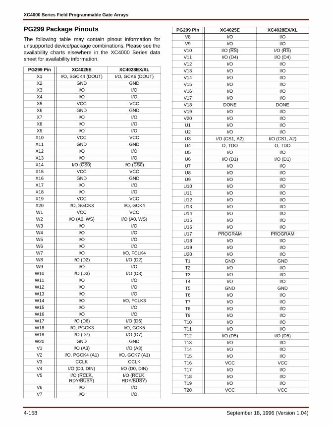
XC4000 Series Field Programmable Gate Arrays
PG299 Package PinoutsThe following table may contain pinout information forunsupported device/package combinations. Please see theavailability charts elsewhere in the XC4000 Series datasheet for availability information.
PG299 Pin XC4025E XC4028EX/XLX1 I/O, SGCK4 (DOUT) I/O, GCK6 (DOUT)
X2 GND GND
X3 I/O I/O
X4 I/O I/O
X5 VCC VCC
X6 GND GND
X7 I/O I/O
X8 I/O I/O
X9 I/O I/O
X10 VCC VCC
X11 GND GND
X12 I/O I/O
X13 I/O I/O
X14 I/O (CS0) I/O (CS0)
X15 VCC VCC
X16 GND GND
X17 I/O I/O
X18 I/O I/O
X19 VCC VCC
X20 I/O, SGCK3 I/O, GCK4
W1 VCC VCC
W2 I/O (A0, WS) I/O (A0, WS)
W3 I/O I/O
W4 I/O I/O
W5 I/O I/O
W6 I/O I/O
W7 I/O I/O, FCLK4
W8 I/O (D2) I/O (D2)
W9 I/O I/O
W10 I/O (D3) I/O (D3)
W11 I/O I/O
W12 I/O I/O
W13 I/O I/O
W14 I/O I/O, FCLK3
W15 I/O I/O
W16 I/O I/O
W17 I/O (D6) I/O (D6)
W18 I/O, PGCK3 I/O, GCK5
W19 I/O (D7) I/O (D7)
W20 GND GND
V1 I/O (A3) I/O (A3)
V2 I/O, PGCK4 (A1) I/O, GCK7 (A1)
V3 CCLK CCLK
V4 I/O (D0, DIN) I/O (D0, DIN)
V5 I/O (RCLK, RDY/BUSY)
I/O (RCLK, RDY/BUSY)
V6 I/O I/O
V7 I/O I/O
V8 I/O I/O
V9 I/O I/O
V10 I/O (RS) I/O (RS)
V11 I/O (D4) I/O (D4)
V12 I/O I/O
V13 I/O I/O
V14 I/O I/O
V15 I/O I/O
V16 I/O I/O
V17 I/O I/O
V18 DONE DONE
V19 I/O I/O
V20 I/O I/O
U1 I/O I/O
U2 I/O I/O
U3 I/O (CS1, A2) I/O (CS1, A2)
U4 O, TDO O, TDO
U5 I/O I/O
U6 I/O (D1) I/O (D1)
U7 I/O I/O
U8 I/O I/O
U9 I/O I/O
U10 I/O I/O
U11 I/O I/O
U12 I/O I/O
U13 I/O I/O
U14 I/O I/O
U15 I/O I/O
U16 I/O I/O
U17 PROGRAM PROGRAM
U18 I/O I/O
U19 I/O I/O
U20 I/O I/O
T1 GND GND
T2 I/O I/O
T3 I/O I/O
T4 I/O I/O
T5 GND GND
T6 I/O I/O
T7 I/O I/O
T8 I/O I/O
T9 I/O I/O
T10 I/O I/O
T11 I/O I/O
T12 I/O (D5) I/O (D5)
T13 I/O I/O
T14 I/O I/O
T15 I/O I/O
T16 VCC VCC
T17 I/O I/O
T18 I/O I/O
T19 I/O I/O
T20 VCC VCC
PG299 Pin XC4025E XC4028EX/XL
4-158 September 18, 1996 (Version 1.04)

R1 VCC VCC
R2 I/O I/O
R3 I/O I/O
R4 I/O I/O
R5 I/O I/O
R16 I/O I/O
R17 I/O I/O
R18 I/O I/O
R19 I/O I/O
R20 GND GND
P1 I/O I/O
P2 I/O I/O
P3 I/O I/O
P4 I/O I/O
P5 I/O I/O
P16 I/O I/O
P17 I/O I/O
P18 I/O I/O
P19 I/O I/O
P20 I/O I/O
N1 I/O (A4) I/O (A4)
N2 I/O I/O
N3 I/O I/O
N4 I/O I/O
N5 I/O I/O
N16 I/O I/O
N17 I/O I/O
N18 I/O I/O
N19 I/O I/O
N20 I/O I/O
M1 I/O I/O (A21)
M2 I/O I/O
M3 I/O (A5) I/O (A5)
M4 I/O I/O
M5 I/O I/O
M16 I/O I/O
M17 I/O I/O
M18 I/O I/O
M19 I/O I/O
M20 I/O I/O
L1 GND GND
L2 I/O (A7) I/O (A7)
L3 I/O (A6) I/O (A6)
L4 I/O I/O (A20)
L5 I/O I/O
L16 I/O I/O
L17 I/O I/O
L18 I/O I/O
L19 I/O I/O
L20 VCC VCC
K1 VCC VCC
K2 I/O (A8) I/O (A8)
K3 I/O (A9) I/O (A9)
PG299 Pin XC4025E XC4028EX/XLK4 I/O I/O (A18)
K5 I/O I/O (A19)
K16 I/O I/O
K17 I/O I/O
K18 I/O I/O
K19 I/O (INIT) I/O (INIT)
K20 GND GND
J1 I/O I/O
J2 I/O I/O
J3 I/O (A11) I/O (A11)
J4 I/O I/O
J5 I/O I/O
J16 I/O I/O
J17 I/O I/O
J18 I/O I/O
J19 I/O I/O
J20 I/O I/O
H1 I/O (A10) I/O (A10)
H2 I/O I/O
H3 I/O I/O
H4 I/O I/O
H5 I/O I/O
H16 I/O I/O
H17 I/O I/O
H18 I/O I/O
H19 I/O I/O
H20 I/O I/O
G1 I/O I/O
G2 I/O I/O
G3 I/O I/O
G4 I/O I/O
G5 I/O (A12) I/O (A12)
G16 I/O I/O
G17 I/O I/O
G18 I/O I/O
G19 I/O I/O
G20 I/O I/O
F1 GND GND
F2 I/O I/O
F3 I/O I/O
F4 I/O I/O
F5 I/O I/O
F16 I/O I/O
F17 I/O I/O
F18 I/O I/O
F19 I/O I/O
F20 VCC VCC
E1 VCC VCC
E2 I/O I/O
E3 I/O I/O
E4 I/O I/O
E5 VCC VCC
E6 I/O I/O
PG299 Pin XC4025E XC4028EX/XL
September 18, 1996 (Version 1.04) 4-159

XC4000 Series Field Programmable Gate Arrays
3/18/96
Note: Shaded pins should be taken into account when de-signing PC boards, in case of future replacement by differ-ent devices.
Note: Viewed from the bottom side, the package pins startat the top row and go from the left edge to the right edge.Viewed from the top side, the pins start at the top row andgo from the right edge to the left edge.
E7 I/O I/O
E8 I/O I/O
E9 I/O I/O
E10 I/O I/O
E11 I/O I/O
E12 I/O I/O
E13 I/O I/O
E14 I/O I/O
E15 I/O I/O
E16 GND GND
E17 I/O I/O
E18 I/O I/O
E19 I/O I/O
E20 GND GND
D1 I/O I/O
D2 I/O I/O
D3 I/O (A14) I/O (A14)
D4 I/O, PGCK1 (A16) I/O, GCK1 (A16)
D5 I/O, TDI I/O, TDI
D6 I/O I/O
D7 I/O I/O
D8 I/O I/O
D9 I/O I/O
D10 I/O I/O
D11 I/O I/O
D12 I/O I/O
D13 I/O I/O, FCLK2
D14 I/O I/O
D15 I/O I/O
D16 I/O I/O
D17 I (M2) I (M2)
D18 I/O I/O
D19 I/O I/O
D20 I/O I/O
C1 I/O (A13) I/O (A13)
C2 I/O I/O
C3 I/O, SGCK1 (A15) I/O, GCK8 (A15)
C4 I/O, TCK I/O, TCK
C5 I/O I/O
C6 I/O I/O
C7 I/O, TMS I/O, TMS
C8 I/O I/O
C9 I/O I/O
C10 I/O I/O
C11 I/O I/O
C12 I/O I/O
C13 I/O I/O
C14 I/O I/O
C15 I/O I/O
C16 I/O I/O
C17 I/O, SGCK2 I/O, GCK2
C18 I (M0) I (M0)
C19 I/O (HDC) I/O (HDC)
PG299 Pin XC4025E XC4028EX/XL
C20 I/O (LDC) I/O (LDC)
B1 GND GND
B2 I/O (A17) I/O (A17)
B3 I/O I/O
B4 I/O I/O
B5 I/O I/O
B6 I/O I/O, FCLK1
B7 I/O I/O
B8 I/O I/O
B9 I/O I/O
B10 I/O I/O
B11 I/O I/O
B12 I/O I/O
B13 I/O I/O
B14 I/O I/O
B15 I/O I/O
B16 I/O I/O
B17 I/O I/O
B18 I/O I/O
B19 I/O, PGCK2 I/O, GCK3
B20 VCC VCC
A2 VCC VCC
A3 I/O I/O
A4 I/O I/O
A5 GND GND
A6 VCC VCC
A7 I/O I/O
A8 I/O I/O
A9 I/O I/O
A10 GND GND
A11 VCC VCC
A12 I/O I/O
A13 I/O I/O
A14 I/O I/O
A15 GND GND
A16 VCC VCC
A17 I/O I/O
A18 I/O I/O
A19 GND GND
A20 O (M1) O (M1)
PG299 Pin XC4025E XC4028EX/XL
4-160 September 18, 1996 (Version 1.04)

HQ304 Package PinoutsThe following table may contain pinout information forunsupported device/package combinations. Please see theavailability charts elsewhere in the XC4000 Series datasheet for availability information.
HQ304 Pin XC4025E XC4028EX
XC4028XLXC4036EXXC4036XL
P1 VCC VCC VCC
P2 I/O, SGCK1 (A15) I/O, GCK8 (A15)
I/O, GCK8(A15)
P3 I/O (A14) I/O (A14) I/O (A14)
P4 I/O I/O I/O
P5 I/O I/O I/O
P6 I/O I/O I/O
P7 I/O I/O I/O
P8 I/O I/O I/O
P9 I/O I/O I/O
P10 I/O (A13) I/O (A13) I/O (A13)
P11 N.C. N.C. N.C.
P12 I/O (A12) I/O (A12) I/O (A12)
P13 I/O I/O I/O
P14 I/O I/O I/O
P15 I/O I/O I/O
P16 I/O I/O I/O
P17 I/O I/O I/O
P18 I/O I/O I/O
P19 GND GND GND
P20 I/O I/O I/O
P21 I/O I/O I/O
P22 I/O I/O I/O
P23 I/O I/O I/O
P24 N.C. N.C. N.C.
P25 VCC VCC VCC
P26 I/O I/O I/O
P27 I/O I/O I/O
P28 I/O I/O I/O
P29 I/O I/O I/O
P30 I/O (A11) I/O (A11) I/O (A11)
P31 I/O (A10) I/O (A10) I/O (A10)
P32 I/O I/O I/O
P33 I/O I/O I/O
P34 I/O I/O (A18) I/O (A18)
P35 I/O I/O (A19) I/O (A19)
P36 I/O (A9) I/O (A9) I/O (A9)
P37 I/O (A8) I/O (A8) I/O (A8)
P38 VCC VCC VCC
P39 GND GND GND
P40 I/O (A7) I/O (A7) I/O (A7)
P41 I/O (A6) I/O (A6) I/O (A6)
P42 I/O I/O (A20) I/O (A20)
P43 I/O I/O (A21) I/O (A21)
P44 I/O I/O I/O
P45 I/O I/O I/O
P46 I/O (A5) I/O (A5) I/O (A5)
P47 I/O (A4) I/O (A4) I/O (A4)
P48 I/O I/O I/O
P49 I/O I/O I/O
P50 I/O I/O I/O
P51 I/O I/O I/O
P52 VCC VCC VCC
P53 N.C. N.C. N.C.
P54 I/O I/O I/O
P55 I/O I/O I/O
P56 I/O I/O I/O
P57 I/O I/O I/O
P58 GND GND GND
P59 I/O I/O I/O
P60 I/O I/O I/O
P61 I/O I/O I/O
P62 I/O I/O I/O
P63 I/O I/O I/O
P64 I/O I/O I/O
P65 I/O I/O I/O
P66 I/O I/O I/O
P67 I/O I/O I/O
P68 I/O I/O I/O
P69 I/O (A3) I/O (A3) I/O (A3)
P70 I/O (CS1, A2) I/O (CS1, A2) I/O (CS1, A2)
P71 I/O I/O I/O
P72 I/O I/O I/O
P73 I/O, PGCK4 (A1) I/O, GCK7 (A1) I/O, GCK7 (A1)
P74 I/O (A0, WS) I/O (A0, WS) I/O (A0, WS)
P75 GND GND GND
P76 O, TDO O, TDO O, TDO
P77 VCC VCC VCC
P78 CCLK CCLK CCLK
P79 I/O, SGCK4 (DOUT)
I/O, GCK6 (DOUT)
I/O, GCK6 (DOUT)
P80 I/O (D0, DIN) I/O (D0, DIN) I/O (D0, DIN)
P81 I/O I/O I/O
P82 I/O I/O I/O
P83 I/O I/O I/O
P84 I/O I/O I/O
P85 I/O (RCLK, RDY/BUSY)
I/O (RCLK, RDY/BUSY)
I/O (RCLK, RDY/BUSY)
P86 I/O (D1) I/O (D1) I/O (D1)
P87 I/O I/O I/O
P88 I/O I/O I/O
P89 I/O I/O I/O
P90 I/O I/O I/O
P91 I/O I/O I/O
P92 I/O I/O I/O
P93 I/O I/O I/O
P94 I/O I/O I/O
P95 GND GND GND
P96 I/O I/O I/O
P97 I/O I/O I/O
P98 I/O I/O, FCLK4 I/O, FCLK4
HQ304 Pin XC4025E XC4028EX
XC4028XLXC4036EXXC4036XL
September 18, 1996 (Version 1.04) 4-161
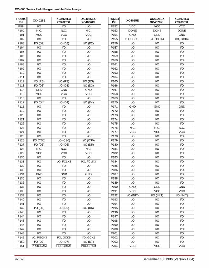
XC4000 Series Field Programmable Gate Arrays
P99 I/O I/O I/O
P100 N.C. N.C. N.C.
P101 VCC VCC VCC
P102 I/O I/O I/O
P103 I/O (D2) I/O (D2) I/O (D2)
P104 I/O I/O I/O
P105 I/O I/O I/O
P106 I/O I/O I/O
P107 I/O I/O I/O
P108 I/O I/O I/O
P109 I/O I/O I/O
P110 I/O I/O I/O
P111 I/O I/O I/O
P112 I/O (RS) I/O (RS) I/O (RS)
P113 I/O (D3) I/O (D3) I/O (D3)
P114 GND GND GND
P115 VCC VCC VCC
P116 I/O I/O I/O
P117 I/O (D4) I/O (D4) I/O (D4)
P118 I/O I/O I/O
P119 I/O I/O I/O
P120 I/O I/O I/O
P121 I/O I/O I/O
P122 I/O I/O I/O
P123 I/O I/O I/O
P124 I/O I/O I/O
P125 I/O I/O I/O
P126 I/O (CS0) I/O (CS0) I/O (CS0)
P127 I/O (D5) I/O (D5) I/O (D5)
P128 N.C. N.C. N.C.
P129 VCC VCC VCC
P130 I/O I/O I/O
P131 I/O I/O, FCLK3 I/O, FCLK3
P132 I/O I/O I/O
P133 I/O I/O I/O
P134 GND GND GND
P135 I/O I/O I/O
P136 I/O I/O I/O
P137 I/O I/O I/O
P138 I/O I/O I/O
P139 I/O I/O I/O
P140 I/O I/O I/O
P141 I/O I/O I/O
P142 I/O (D6) I/O (D6) I/O (D6)
P143 I/O I/O I/O
P144 I/O I/O I/O
P145 I/O I/O I/O
P146 I/O I/O I/O
P147 I/O I/O I/O
P148 I/O I/O I/O
P149 I/O, PGCK3 I/O, GCK5 I/O, GCK5
P150 I/O (D7) I/O (D7) I/O (D7)
P151 PROGRAM PROGRAM PROGRAM
HQ304 Pin XC4025E XC4028EX
XC4028XLXC4036EXXC4036XL
P152 VCC VCC VCC
P153 DONE DONE DONE
P154 GND GND GND
P155 I/O, SGCK3 I/O, GCK4 I/O, GCK4
P156 I/O I/O I/O
P157 I/O I/O I/O
P158 I/O I/O I/O
P159 I/O I/O I/O
P160 I/O I/O I/O
P161 I/O I/O I/O
P162 I/O I/O I/O
P163 I/O I/O I/O
P164 I/O I/O I/O
P165 I/O I/O I/O
P166 I/O I/O I/O
P167 I/O I/O I/O
P168 I/O I/O I/O
P169 I/O I/O I/O
P170 I/O I/O I/O
P171 GND GND GND
P172 I/O I/O I/O
P173 I/O I/O I/O
P174 I/O I/O I/O
P175 I/O I/O I/O
P176 N.C. N.C. N.C.
P177 VCC VCC VCC
P178 I/O I/O I/O
P179 I/O I/O I/O
P180 I/O I/O I/O
P181 I/O I/O I/O
P182 I/O I/O I/O
P183 I/O I/O I/O
P184 I/O I/O I/O
P185 I/O I/O I/O
P186 I/O I/O I/O
P187 I/O I/O I/O
P188 I/O I/O I/O
P189 I/O I/O I/O
P190 GND GND GND
P191 VCC VCC VCC
P192 I/O (INIT) I/O (INIT) I/O (INIT)
P193 I/O I/O I/O
P194 I/O I/O I/O
P195 I/O I/O I/O
P196 I/O I/O I/O
P197 I/O I/O I/O
P198 I/O I/O I/O
P199 I/O I/O I/O
P200 I/O I/O I/O
P201 I/O I/O I/O
P202 I/O I/O I/O
P203 I/O I/O I/O
P204 VCC VCC VCC
HQ304 Pin XC4025E XC4028EX
XC4028XLXC4036EXXC4036XL
4-162 September 18, 1996 (Version 1.04)

3/20/96
Note: Shaded pins should be taken into account when de-signing PC boards, in case of future replacement by differ-ent devices.
P205 N.C. N.C. N.C.
P206 I/O I/O I/O
P207 I/O I/O I/O
P208 I/O I/O I/O
P209 I/O I/O I/O
P210 GND GND GND
P211 I/O I/O I/O
P212 I/O I/O I/O
P213 I/O I/O I/O
P214 I/O I/O I/O
P215 I/O I/O I/O
P216 I/O I/O I/O
P217 I/O I/O I/O
P218 I/O I/O I/O
P219 I/O I/O I/O
P220 I/O I/O I/O
P221 I/O (LDC) I/O (LDC) I/O (LDC)
P222 I/O I/O I/O
P223 I/O I/O I/O
P224 I/O I/O I/O
P225 I/O (HDC) I/O (HDC) I/O (HDC)
P226 I/O, PGCK2 I/O, GCK3 I/O, GCK3
P227 I (M2) I (M2) I (M2)
P228 VCC VCC VCC
P229 I (M0) I (M0) I (M0)
P230 GND GND GND
P231 O (M1) O (M1) O (M1)
P232 I/O, SGCK2 I/O, GCK2 I/O, GCK2
P233 I/O I/O I/O
P234 I/O I/O I/O
P235 I/O I/O I/O
P236 I/O I/O I/O
P237 I/O I/O I/O
P238 I/O I/O I/O
P239 I/O I/O I/O
P240 I/O I/O I/O
P241 I/O I/O I/O
P242 I/O I/O I/O
P243 I/O I/O I/O
P244 I/O I/O I/O
P245 I/O I/O I/O
P246 I/O I/O I/O
P247 I/O I/O I/O
P248 GND GND GND
P249 I/O I/O, FCLK2 I/O, FCLK2
P250 I/O I/O I/O
P251 I/O I/O I/O
P252 I/O I/O I/O
P253 VCC VCC VCC
P254 N.C. N.C. N.C.
P255 I/O I/O I/O
P256 I/O I/O I/O
P257 I/O I/O I/O
HQ304 Pin XC4025E XC4028EX
XC4028XLXC4036EXXC4036XL
P258 I/O I/O I/O
P259 I/O I/O I/O
P260 I/O I/O I/O
P261 I/O I/O I/O
P262 I/O I/O I/O
P263 I/O I/O I/O
P264 I/O I/O I/O
P265 I/O I/O I/O
P266 I/O I/O I/O
P267 VCC VCC VCC
P268 GND GND GND
P269 I/O I/O I/O
P270 I/O I/O I/O
P271 I/O I/O I/O
P272 I/O I/O I/O
P273 I/O I/O I/O
P274 I/O I/O I/O
P275 I/O I/O I/O
P276 I/O I/O I/O
P277 I/O I/O I/O
P278 I/O I/O I/O
P279 I/O I/O I/O
P280 I/O I/O I/O
P281 N.C. N.C. N.C.
P282 VCC VCC VCC
P283 I/O I/O I/O
P284 I/O, TMS I/O, TMS I/O, TMS
P285 I/O I/O I/O
P286 I/O I/O, FCLK1 I/O, FCLK1
P287 GND GND GND
P288 I/O I/O I/O
P289 I/O I/O I/O
P290 I/O I/O I/O
P291 I/O I/O I/O
P292 I/O I/O I/O
P293 I/O I/O I/O
P294 I/O I/O I/O
P295 I/O I/O I/O
P296 I/O I/O I/O
P297 I/O I/O I/O
P298 I/O, TCK I/O, TCK I/O, TCK
P299 I/O, TDI I/O, TDI I/O, TDI
P300 I/O I/O I/O
P301 I/O I/O I/O
P302 I/O (A17) I/O (A17) I/O (A17)
P303 I/O, PGCK1 (A16)
I/O, GCK1 (A16)
I/O, GCK1 (A16)
P304 GND GND GND
HQ304 Pin XC4025E XC4028EX
XC4028XLXC4036EXXC4036XL
September 18, 1996 (Version 1.04) 4-163
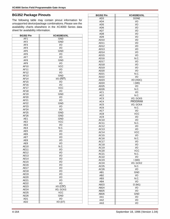
XC4000 Series Field Programmable Gate Arrays
BG352 Package PinoutsThe following table may contain pinout information forunsupported device/package combinations. Please see theavailability charts elsewhere in the XC4000 Series datasheet for availability information.
BG352 Pin XC4028EX/XLAF1 GNDAF2 GNDAF3 I/OAF4 I/OAF5 GNDAF6 I/OAF7 I/OAF8 GNDAF9 I/OAF10 VCCAF11 I/OAF12 I/OAF13 GNDAF14 I/O (INIT)AF15 I/OAF16 I/OAF17 VCCAF18 I/OAF19 GNDAF20 I/OAF21 I/OAF22 GNDAF23 I/OAF24 I/OAF25 GNDAF26 GNDAE1 GNDAE2 VCCAE3 I/OAE4 N.C.AE5 I/OAE6 I/OAE7 I/OAE8 I/OAE9 I/OAE10 N.C.AE11 I/OAE12 I/OAE13 I/OAE14 I/OAE15 I/OAE16 I/OAE17 I/OAE18 I/OAE19 I/OAE20 I/OAE21 I/OAE22 I/OAE23 I/O (LDC)AE24 I/O, GCK3AE25 VCCAE26 GNDAD1 I/OAD2 I/O (D7)
AD3 DONEAD4 I/OAD5 I/OAD6 I/OAD7 I/OAD8 I/OAD9 I/O
AD10 I/OAD11 I/OAD12 I/OAD13 I/OAD14 I/OAD15 I/OAD16 N.C.AD17 I/OAD18 I/OAD19 I/OAD20 I/OAD21 N.C.AD22 I/OAD23 I/O (HDC)AD24 I (M0)AD25 I/OAD26 N.C.AC1 I/OAC2 N.C.AC3 I/O, GCK5AC4 PROGRAMAC5 I/O, GCK4AC6 N.C.AC7 I/OAC8 VCCAC9 I/O
AC10 I/OAC11 N.C.AC12 I/OAC13 I/OAC14 VCCAC15 I/OAC16 N.C.AC17 I/OAC18 I/OAC19 I/OAC20 VCCAC21 N.C.AC22 I/OAC23 I (M2)AC24 I/O, GCK2AC25 N.C.AC26 I/OAB1 GNDAB2 I/OAB3 N.C.AB4 I/O
AB23 O (M1)AB24 I/OAB25 I/OAB26 GNDAA1 I/OAA2 I/OAA3 I/O
BG352 Pin XC4028EX/XL
4-164 September 18, 1996 (Version 1.04)

AA4 I/OAA23 I/OAA24 I/OAA25 I/OAA26 I/O
Y1 I/OY2 I/OY3 I/O (D6)Y4 VCCY23 I/OY24 I/OY25 I/OY26 I/OW1 GNDW2 I/OW3 I/OW4 I/OW23 VCCW24 I/OW25 I/OW26 GNDV1 I/O (CS0)V2 I/O (D5)V3 I/OV4 I/OV23 I/OV24 I/OV25 I/OV26 I/OU1 VCCU2 I/OU3 I/OU4 I/O, FCLK3U23 I/O, FCLK2U24 I/OU25 N.C.U26 VCCT1 I/OT2 I/OT3 N.C.T4 N.C.T23 I/OT24 N.C.T25 I/OT26 I/OR1 I/OR2 I/OR3 I/OR4 I/OR23 I/OR24 I/OR25 I/OR26 I/OP1 I/OP2 I/O (D4)P3 I/OP4 VCCP23 I/OP24 I/OP25 I/OP26 GND
BG352 Pin XC4028EX/XLN1 GNDN2 I/O (D3)N3 I/ON4 I/O (RS)N23 VCCN24 I/ON25 I/ON26 I/OM1 I/OM2 I/OM3 I/OM4 I/O
M23 I/OM24 I/OM25 I/OM26 I/OL1 I/OL2 I/OL3 I/OL4 N.C.
L23 N.C.L24 I/OL25 I/OL26 I/OK1 VCCK2 N.C.K3 I/OK4 I/O
K23 I/OK24 I/OK25 I/OK26 VCCJ1 I/O (D2)J2 I/OJ3 I/O, FCLK4J4 I/O
J23 I/O, FCLK1J24 I/OJ25 I/OJ26 N.C.H1 GNDH2 I/OH3 I/OH4 VCC
H23 I/OH24 I/OH25 I/O, TMSH26 GNDG1 I/OG2 I/OG3 I/OG4 I/O (RCLK, RDY/BUSY)G23 VCCG24 I/OG25 I/OG26 I/OF1 I/OF2 I/OF3 I/O (D1)F4 I/O
F23 N.C.
BG352 Pin XC4028EX/XL
September 18, 1996 (Version 1.04) 4-165

XC4000 Series Field Programmable Gate Arrays
2/28/96
Note: Viewed from the bottom side, the package pins startat the top row and go from the left edge to the right edge.Viewed from the top side, the pins start at the top row andgo from the right edge to the left edge.
F24 I/OF25 I/OF26 I/OE1 GNDE2 I/OE3 I/OE4 I/O, GCK6 (DOUT)E23 I/OE24 I/O, TCKE25 I/OE26 GNDD1 N.C.D2 I/OD3 I/O (D0, DIN)D4 O (TDO)D5 I/OD6 I/O (CS1, A2)D7 VCCD8 I/OD9 I/OD10 I/OD11 I/OD12 I/O (A4)D13 VCCD14 I/O (A8)D15 I/OD16 N.C.D17 I/OD18 I/OD19 VCCD20 I/OD21 I/OD22 I/O (A14)D23 I/O, GCK1 (A16)D24 I/OD25 N.C.D26 I/OC1 N.C.C2 I/OC3 CCLKC4 I/O, GCK7 (A1)C5 N.C.C6 I/O (A3)C7 I/OC8 N.C.C9 I/OC10 I/OC11 N.C.C12 I/O (A5)C13 I/O (A21)C14 I/O (A9)C15 I/OC16 I/OC17 I/OC18 I/OC19 I/OC20 I/OC21 I/O (A13)C22 I/OC23 I/OC24 I/O, GCK8 (A15)
BG352 Pin XC4028EX/XLC25 I/O (A17)C26 I/O, TDIB1 GNDB2 VCCB3 I/O (A0, WS)B4 N.C.B5 I/OB6 I/OB7 I/OB8 I/OB9 I/O
B10 N.C.B11 I/OB12 I/OB13 I/O (A20)B14 I/O (A7)B15 I/O (A18)B16 I/O (A11)B17 I/OB18 I/OB19 I/OB20 I/OB21 I/OB22 I/O (A12)B23 N.C.B24 I/OB25 VCCB26 GNDA1 GNDA2 GNDA3 I/OA4 I/OA5 GNDA6 I/OA7 I/OA8 GNDA9 I/O
A10 VCCA11 I/OA12 I/OA13 I/O (A6)A14 GNDA15 I/O (A19)A16 I/O (A10)A17 VCCA18 N.C.A19 GNDA20 I/OA21 I/OA22 GNDA23 I/OA24 N.C.A25 GNDA26 GND
BG352 Pin XC4028EX/XL
4-166 September 18, 1996 (Version 1.04)
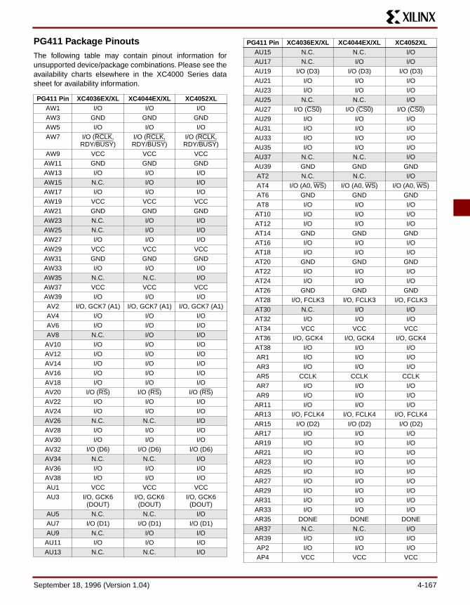
PG411 Package PinoutsThe following table may contain pinout information forunsupported device/package combinations. Please see theavailability charts elsewhere in the XC4000 Series datasheet for availability information.
PG411 Pin XC4036EX/XL XC4044EX/XL XC4052XLAW1 I/O I/O I/O
AW3 GND GND GND
AW5 I/O I/O I/O
AW7 I/O (RCLK, RDY/BUSY)
I/O (RCLK, RDY/BUSY)
I/O (RCLK, RDY/BUSY)
AW9 VCC VCC VCC
AW11 GND GND GND
AW13 I/O I/O I/O
AW15 N.C. I/O I/O
AW17 I/O I/O I/O
AW19 VCC VCC VCC
AW21 GND GND GND
AW23 N.C. I/O I/O
AW25 N.C. I/O I/O
AW27 I/O I/O I/O
AW29 VCC VCC VCC
AW31 GND GND GND
AW33 I/O I/O I/O
AW35 N.C. N.C. I/O
AW37 VCC VCC VCC
AW39 I/O I/O I/O
AV2 I/O, GCK7 (A1) I/O, GCK7 (A1) I/O, GCK7 (A1)
AV4 I/O I/O I/O
AV6 I/O I/O I/O
AV8 N.C. I/O I/O
AV10 I/O I/O I/O
AV12 I/O I/O I/O
AV14 I/O I/O I/O
AV16 I/O I/O I/O
AV18 I/O I/O I/O
AV20 I/O (RS) I/O (RS) I/O (RS)
AV22 I/O I/O I/O
AV24 I/O I/O I/O
AV26 N.C. N.C. I/O
AV28 I/O I/O I/O
AV30 I/O I/O I/O
AV32 I/O (D6) I/O (D6) I/O (D6)
AV34 N.C. N.C. I/O
AV36 I/O I/O I/O
AV38 I/O I/O I/O
AU1 VCC VCC VCC
AU3 I/O, GCK6 (DOUT)
I/O, GCK6 (DOUT)
I/O, GCK6 (DOUT)
AU5 N.C. N.C. I/O
AU7 I/O (D1) I/O (D1) I/O (D1)
AU9 N.C. I/O I/O
AU11 I/O I/O I/O
AU13 N.C. N.C. I/O
AU15 N.C. N.C. I/O
AU17 N.C. I/O I/O
AU19 I/O (D3) I/O (D3) I/O (D3)
AU21 I/O I/O I/O
AU23 I/O I/O I/O
AU25 N.C. N.C. I/O
AU27 I/O (CS0) I/O (CS0) I/O (CS0)
AU29 I/O I/O I/O
AU31 I/O I/O I/O
AU33 I/O I/O I/O
AU35 I/O I/O I/O
AU37 N.C. N.C. I/O
AU39 GND GND GND
AT2 N.C. N.C. I/O
AT4 I/O (A0, WS) I/O (A0, WS) I/O (A0, WS)
AT6 GND GND GND
AT8 I/O I/O I/O
AT10 I/O I/O I/O
AT12 I/O I/O I/O
AT14 GND GND GND
AT16 I/O I/O I/O
AT18 I/O I/O I/O
AT20 GND GND GND
AT22 I/O I/O I/O
AT24 I/O I/O I/O
AT26 GND GND GND
AT28 I/O, FCLK3 I/O, FCLK3 I/O, FCLK3
AT30 N.C. I/O I/O
AT32 I/O I/O I/O
AT34 VCC VCC VCC
AT36 I/O, GCK4 I/O, GCK4 I/O, GCK4
AT38 I/O I/O I/O
AR1 I/O I/O I/O
AR3 I/O I/O I/O
AR5 CCLK CCLK CCLK
AR7 I/O I/O I/O
AR9 I/O I/O I/O
AR11 I/O I/O I/O
AR13 I/O, FCLK4 I/O, FCLK4 I/O, FCLK4
AR15 I/O (D2) I/O (D2) I/O (D2)
AR17 I/O I/O I/O
AR19 I/O I/O I/O
AR21 I/O I/O I/O
AR23 I/O I/O I/O
AR25 I/O I/O I/O
AR27 I/O I/O I/O
AR29 I/O I/O I/O
AR31 I/O I/O I/O
AR33 I/O I/O I/O
AR35 DONE DONE DONE
AR37 N.C. N.C. I/O
AR39 I/O I/O I/O
AP2 I/O I/O I/O
AP4 VCC VCC VCC
PG411 Pin XC4036EX/XL XC4044EX/XL XC4052XL
September 18, 1996 (Version 1.04) 4-167

XC4000 Series Field Programmable Gate Arrays
AP6 I/O (D0, DIN) I/O (D0, DIN) I/O (D0, DIN)
AP8 N.C. N.C. I/O
AP10 I/O I/O I/O
AP12 I/O I/O I/O
AP14 I/O I/O I/O
AP16 I/O I/O I/O
AP18 I/O I/O I/O
AP20 I/O (D4) I/O (D4) I/O (D4)
AP22 I/O I/O I/O
AP24 I/O (D5) I/O (D5) I/O (D5)
AP26 I/O I/O I/O
AP28 I/O I/O I/O
AP30 N.C. I/O I/O
AP32 I/O I/O I/O
AP34 I/O, GCK5 I/O, GCK5 I/O, GCK5
AP36 GND GND GND
AP38 N.C. I/O I/O
AN1 N.C. I/O I/O
AN3 I/O (A3) I/O (A3) I/O (A3)
AN5 N.C. N.C. I/O
AN7 O, TDO O, TDO O, TDO
AN9 I/O I/O I/O
AN31 I/O I/O I/O
AN33 PROGRAM PROGRAM PROGRAM
AN35 I/O I/O I/O
AN37 I/O I/O I/O
AN39 I/O I/O I/O
AM2 I/O I/O I/O
AM4 I/O I/O I/O
AM6 I/O I/O I/O
AM8 I/O I/O I/O
AM32 I/O (D7) I/O (D7) I/O (D7)
AM34 I/O I/O I/O
AM36 I/O I/O I/O
AM38 I/O I/O I/O
AL1 GND GND GND
AL3 I/O I/O I/O
AL5 I/O I/O I/O
AL7 I/O I/O I/O
AL33 I/O I/O I/O
AL35 N.C. N.C. I/O
AL37 I/O I/O I/O
AL39 VCC VCC VCC
AK2 N.C. I/O I/O
AK4 I/O I/O I/O
AK6 I/O (CS1, A2) I/O (CS1, A2) I/O (CS1, A2)
AK34 I/O I/O I/O
AK36 I/O I/O I/O
AK38 N.C. I/O I/O
AJ1 VCC VCC VCC
AJ3 I/O I/O I/O
AJ5 N.C. N.C. I/O
AJ35 I/O I/O I/O
AJ37 I/O I/O I/O
PG411 Pin XC4036EX/XL XC4044EX/XL XC4052XLAJ39 GND GND GND
AH2 I/O I/O I/O
AH4 I/O I/O I/O
AH6 I/O I/O I/O
AH34 I/O I/O I/O
AH36 I/O I/O I/O
AH38 I/O I/O I/O
AG1 I/O I/O I/O
AG3 I/O I/O I/O
AG5 I/O I/O I/O
AG35 I/O I/O I/O
AG37 I/O I/O I/O
AG39 I/O I/O I/O
AF2 N.C. N.C. I/O
AF4 GND GND GND
AF6 I/O I/O I/O
AF34 I/O I/O I/O
AF36 GND GND GND
AF38 N.C. N.C. I/O
AE1 I/O I/O I/O
AE3 I/O I/O I/O
AE5 I/O I/O I/O
AE35 I/O I/O I/O
AE37 I/O I/O I/O
AE39 I/O I/O I/O
AD2 I/O (A4) I/O (A4) I/O (A4)
AD4 I/O (A21) I/O (A21) I/O (A21)
AD6 I/O I/O I/O
AD34 I/O I/O I/O
AD36 I/O I/O I/O
AD38 I/O I/O I/O
AC1 I/O I/O I/O
AC3 N.C. I/O I/O
AC5 I/O I/O I/O
AC35 I/O I/O I/O
AC37 I/O I/O I/O
AC39 N.C. I/O I/O
AB2 N.C. I/O I/O
AB4 I/O (A5) I/O (A5) I/O (A5)
AB6 I/O I/O I/O
AB34 I/O I/O I/O
AB36 I/O I/O I/O
AB38 I/O I/O I/O
AA1 GND GND GND
AA3 I/O (A6) I/O (A6) I/O (A6)
AA5 I/O (A20) I/O (A20) I/O (A20)
AA35 I/O I/O I/O
AA37 N.C. I/O I/O
AA39 VCC VCC VCC
Y2 I/O (A9) I/O (A9) I/O (A9)
Y4 GND GND GND
Y6 I/O (A7) I/O (A7) I/O (A7)
Y34 I/O I/O I/O
Y36 GND GND GND
PG411 Pin XC4036EX/XL XC4044EX/XL XC4052XL
4-168 September 18, 1996 (Version 1.04)

Y38 N.C. I/O I/O
W1 VCC VCC VCC
W3 I/O (A8) I/O (A8) I/O (A8)
W5 N.C. I/O I/O
W35 N.C. I/O I/O
W37 I/O (INIT) I/O (INIT) I/O (INIT)
W39 GND GND GND
V2 N.C. I/O I/O
V4 I/O (A19) I/O (A19) I/O (A19)
V6 I/O I/O I/O
V34 I/O I/O I/O
V36 I/O I/O I/O
V38 I/O I/O I/O
U1 I/O I/O I/O
U3 I/O (A10) I/O (A10) I/O (A10)
U5 I/O I/O I/O
U35 I/O I/O I/O
U37 I/O I/O I/O
U39 I/O I/O I/O
T2 I/O (A18) I/O (A18) I/O (A18)
T4 I/O I/O I/O
T6 I/O I/O I/O
T34 I/O I/O I/O
T36 I/O I/O I/O
T38 I/O I/O I/O
R1 I/O (A11) I/O (A11) I/O (A11)
R3 N.C. N.C. I/O
R5 I/O I/O I/O
R35 I/O I/O I/O
R37 I/O I/O I/O
R39 I/O I/O I/O
P2 I/O I/O I/O
P4 GND GND GND
P6 I/O I/O I/O
P34 I/O I/O I/O
P36 GND GND GND
P38 N.C. N.C. I/O
N1 I/O I/O I/O
N3 N.C. N.C. I/O
N5 I/O I/O I/O
N35 I/O I/O I/O
N37 I/O I/O I/O
N39 I/O I/O I/O
M2 I/O I/O I/O
M4 I/O I/O I/O
M6 I/O I/O I/O
M34 I/O I/O I/O
M36 I/O I/O I/O
M38 I/O I/O I/O
L1 GND GND GND
L3 I/O I/O I/O
L5 N.C. I/O I/O
L35 N.C. N.C. I/O
L37 I/O I/O I/O
PG411 Pin XC4036EX/XL XC4044EX/XL XC4052XLL39 VCC VCC VCC
K2 I/O I/O I/O
K4 I/O I/O I/O
K6 I/O I/O I/O
K34 I/O I/O I/O
K36 N.C. I/O I/O
K38 N.C. I/O I/O
J1 VCC VCC VCC
J3 I/O I/O I/O
J5 N.C. I/O I/O
J7 I/O I/O I/O
J33 I/O I/O I/O
J35 I/O I/O I/O
J37 I/O I/O I/O
J39 GND GND GND
H2 I/O I/O I/O
H4 I/O (A12) I/O (A12) I/O (A12)
H6 I/O I/O I/O
H8 I/O, GCK1 (A16) I/O, GCK1 (A16) I/O, GCK1 (A16)
H32 I/O I/O I/O
H34 N.C. N.C. I/O
H36 I/O I/O I/O
H38 I/O I/O I/O
G1 I/O I/O I/O
G3 I/O (A13) I/O (A13) I/O (A13)
G5 N.C. N.C. I/O
G7 I/O, GCK8 (A15) I/O, GCK8 (A15) I/O, GCK8 (A15)
G9 I/O, TCK I/O, TCK I/O, TCK
G31 I/O I/O I/O
G33 I (M2) I (M2) I (M2)
G35 I/O (LDC) I/O (LDC) I/O (LDC)
G37 I/O I/O I/O
G39 I/O I/O I/O
F2 N.C. N.C. I/O
F4 GND GND GND
F6 I/O (A17) i/O (A17) i/O (A17)
F8 I/O I/O I/O
F10 I/O I/O I/O
F12 I/O I/O I/O
F14 I/O I/O I/O
F16 I/O I/O I/O
F18 N.C. I/O I/O
F20 I/O I/O I/O
F22 N.C. I/O I/O
F24 I/O I/O I/O
F26 I/O I/O I/O
F28 I/O I/O I/O
F30 I/O I/O I/O
F32 I/O I/O I/O
F34 I/O I/O I/O
F36 VCC VCC VCC
F38 I/O I/O I/O
E1 I/O I/O I/O
E3 I/O I/O I/O
PG411 Pin XC4036EX/XL XC4044EX/XL XC4052XL
September 18, 1996 (Version 1.04) 4-169

XC4000 Series Field Programmable Gate Arrays
8/23/96
Note: Shaded pins should be taken into account when de-signing PC boards, in case of future replacement by differ-ent devices.
Note: Viewed from the bottom side, the package pins startat the top row and go from the left edge to the right edge.Viewed from the top side, the pins start at the top row andgo from the right edge to the left edge.
E5 I/O (A14) I/O (A14) I/O (A14)
E7 N.C. N.C. I/O
E9 I/O I/O I/O
E11 I/O, TMS I/O, TMS I/O, TMS
E13 I/O I/O I/O
E15 I/O I/O I/O
E17 I/O I/O I/O
E19 I/O I/O I/O
E21 I/O I/O I/O
E23 N.C. N.C. I/O
E25 I/O I/O I/O
E27 I/O I/O I/O
E29 I/O I/O I/O
E31 I/O I/O I/O
E33 I/O I/O I/O
E35 I (M0) I (M0) I (M0)
E37 N.C. N.C. I/O
E39 I/O I/O I/O
D2 I/O I/O I/O
D4 I/O I/O I/O
D6 VCC VCC VCC
D8 N.C. I/O I/O
D10 I/O I/O I/O
D12 N.C. N.C. I/O
D14 GND GND GND
D16 I/O I/O I/O
D18 I/O I/O I/O
D20 GND GND GND
D22 I/O I/O I/O
D24 I/O I/O I/O
D26 GND GND GND
D28 I/O I/O I/O
D30 N.C. I/O I/O
D32 N.C. I/O I/O
D34 GND GND GND
D36 I/O, GCK3 I/O, GCK3 I/O, GCK3
D38 I/O I/O I/O
C1 GND GND GND
C3 I/O I/O I/O
C5 I/O I/O I/O
C7 N.C. I/O I/O
C9 I/O I/O I/O
C11 I/O, FCLK1 I/O, FCLK1 I/O, FCLK1
C13 I/O I/O I/O
C15 N.C. I/O I/O
C17 I/O I/O I/O
C19 I/O I/O I/O
C21 I/O I/O I/O
C23 N.C. I/O I/O
C25 N.C. N.C. I/O
C27 I/O I/O I/O
C29 I/O, FCLK2 I/O, FCLK2 I/O, FCLK2
C31 I/O I/O I/O
C33 N.C. N.C. I/O
PG411 Pin XC4036EX/XL XC4044EX/XL XC4052XLC35 I/O I/O I/O
C37 I/O (HDC) I/O (HDC) I/O (HDC)
C39 VCC VCC VCC
B2 I/O, TDI I/O, TDI I/O, TDI
B4 I/O I/O I/O
B6 N.C. N.C. I/O
B8 I/O I/O I/O
B10 I/O I/O I/O
B12 I/O I/O I/O
B14 I/O I/O I/O
B16 I/O I/O I/O
B18 I/O I/O I/O
B20 I/O I/O I/O
B22 I/O I/O I/O
B24 I/O I/O I/O
B26 I/O I/O I/O
B28 I/O I/O I/O
B30 I/O I/O I/O
B32 I/O I/O I/O
B34 N.C. N.C. I/O
B36 I/O, GCK2 I/O, GCK2 I/O, GCK2
B38 I/O I/O I/O
A3 VCC VCC VCC
A5 I/O I/O I/O
A7 I/O I/O I/O
A9 GND GND GND
A11 VCC VCC VCC
A13 N.C. N.C. I/O
A15 I/O I/O I/O
A17 I/O I/O I/O
A19 GND GND GND
A21 VCC VCC VCC
A23 I/O I/O I/O
A25 I/O I/O I/O
A27 I/O I/O I/O
A29 GND GND GND
A31 VCC VCC VCC
A33 I/O I/O I/O
A35 I/O I/O I/O
A37 GND GND GND
A39 O (M1) O (M1) O (M1)
PG411 Pin XC4036EX/XL XC4044EX/XL XC4052XL
4-170 September 18, 1996 (Version 1.04)
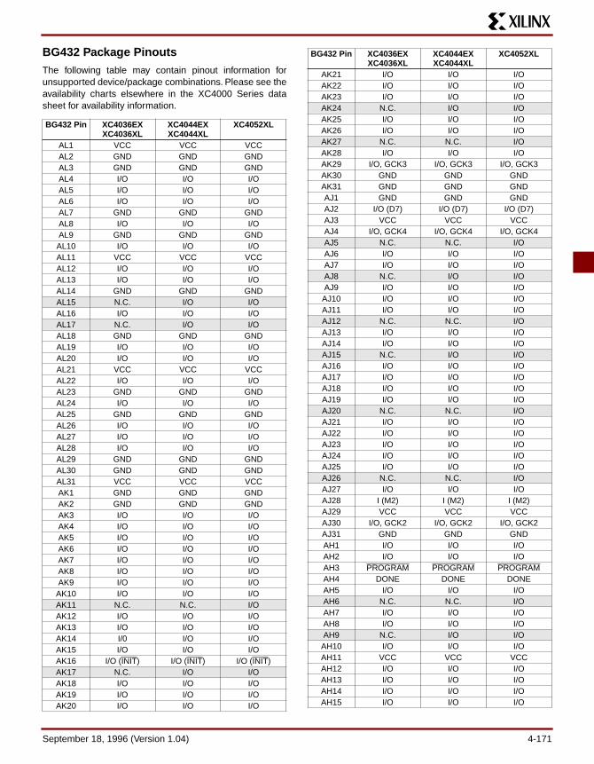
BG432 Package PinoutsThe following table may contain pinout information forunsupported device/package combinations. Please see theavailability charts elsewhere in the XC4000 Series datasheet for availability information.
BG432 Pin XC4036EXXC4036XL
XC4044EXXC4044XL
XC4052XL
AL1 VCC VCC VCCAL2 GND GND GNDAL3 GND GND GNDAL4 I/O I/O I/OAL5 I/O I/O I/OAL6 I/O I/O I/OAL7 GND GND GNDAL8 I/O I/O I/OAL9 GND GND GNDAL10 I/O I/O I/OAL11 VCC VCC VCCAL12 I/O I/O I/OAL13 I/O I/O I/OAL14 GND GND GNDAL15 N.C. I/O I/OAL16 I/O I/O I/OAL17 N.C. I/O I/OAL18 GND GND GNDAL19 I/O I/O I/OAL20 I/O I/O I/OAL21 VCC VCC VCCAL22 I/O I/O I/OAL23 GND GND GNDAL24 I/O I/O I/OAL25 GND GND GNDAL26 I/O I/O I/OAL27 I/O I/O I/OAL28 I/O I/O I/OAL29 GND GND GNDAL30 GND GND GNDAL31 VCC VCC VCCAK1 GND GND GNDAK2 GND GND GNDAK3 I/O I/O I/OAK4 I/O I/O I/OAK5 I/O I/O I/OAK6 I/O I/O I/OAK7 I/O I/O I/OAK8 I/O I/O I/OAK9 I/O I/O I/OAK10 I/O I/O I/OAK11 N.C. N.C. I/OAK12 I/O I/O I/OAK13 I/O I/O I/OAK14 I/0 I/O I/OAK15 I/O I/O I/OAK16 I/O (INIT) I/O (INIT) I/O (INIT)AK17 N.C. I/O I/OAK18 I/O I/O I/OAK19 I/O I/O I/OAK20 I/O I/O I/O
AK21 I/O I/O I/OAK22 I/O I/O I/OAK23 I/O I/O I/OAK24 N.C. I/O I/OAK25 I/O I/O I/OAK26 I/O I/O I/OAK27 N.C. N.C. I/OAK28 I/O I/O I/OAK29 I/O, GCK3 I/O, GCK3 I/O, GCK3AK30 GND GND GNDAK31 GND GND GNDAJ1 GND GND GNDAJ2 I/O (D7) I/O (D7) I/O (D7)AJ3 VCC VCC VCCAJ4 I/O, GCK4 I/O, GCK4 I/O, GCK4AJ5 N.C. N.C. I/OAJ6 I/O I/O I/OAJ7 I/O I/O I/OAJ8 N.C. I/O I/OAJ9 I/O I/O I/O
AJ10 I/O I/O I/OAJ11 I/O I/O I/OAJ12 N.C. N.C. I/OAJ13 I/O I/O I/OAJ14 I/O I/O I/OAJ15 N.C. I/O I/OAJ16 I/O I/O I/OAJ17 I/O I/O I/OAJ18 I/O I/O I/OAJ19 I/O I/O I/OAJ20 N.C. N.C. I/OAJ21 I/O I/O I/OAJ22 I/O I/O I/OAJ23 I/O I/O I/OAJ24 I/O I/O I/OAJ25 I/O I/O I/OAJ26 N.C. N.C. I/OAJ27 I/O I/O I/OAJ28 I (M2) I (M2) I (M2)AJ29 VCC VCC VCCAJ30 I/O, GCK2 I/O, GCK2 I/O, GCK2AJ31 GND GND GNDAH1 I/O I/O I/OAH2 I/O I/O I/OAH3 PROGRAM PROGRAM PROGRAMAH4 DONE DONE DONEAH5 I/O I/O I/OAH6 N.C. N.C. I/OAH7 I/O I/O I/OAH8 I/O I/O I/OAH9 N.C. I/O I/OAH10 I/O I/O I/OAH11 VCC VCC VCCAH12 I/O I/O I/OAH13 I/O I/O I/OAH14 I/O I/O I/OAH15 I/O I/O I/O
BG432 Pin XC4036EXXC4036XL
XC4044EXXC4044XL
XC4052XL
September 18, 1996 (Version 1.04) 4-171

XC4000 Series Field Programmable Gate Arrays
AH16 GND GND GNDAH17 I/O I/O I/OAH18 I/O I/O I/OAH19 N.C. N.C. I/OAH20 I/O I/O I/OAH21 VCC VCC VCCAH22 I/O I/O I/OAH23 N.C. I/O I/OAH24 I/O I/O I/OAH25 I/O I/O I/OAH26 I/O (LDC) I/O (LDC) I/O (LDC)AH27 I/O (HDC) I/O (HDC) I/O (HDC)AH28 I (M0) I (M0) I (M0)AH29 O (M1) O (M1) O (M1)AH30 I/O I/O I/OAH31 I/O I/O I/OAG1 N.C. N.C. I/OAG2 I/O I/O I/OAG3 I/O I/O I/OAG4 I/O, GCK5 I/O, GCK5 I/O, GCK5AG28 I/O I/O I/OAG29 I/O I/O I/OAG30 I/O I/O I/OAG31 I/O I/O I/OAF1 I/O (D6) I/O (D6) I/O (D6)AF2 I/O I/O I/OAF3 I/O I/O I/OAF4 I/O I/O I/OAF28 I/O I/O I/OAF29 N.C. N.C. I/OAF30 N.C. N.C. I/OAF31 I/O I/O I/OAE1 GND GND GNDAE2 I/O I/O I/OAE3 I/O I/O I/OAE4 N.C. N.C. I/OAE28 I/O I/O I/OAE29 I/O I/O I/OAE30 I/O I/O I/OAE31 GND GND GNDAD1 I/O I/O I/OAD2 N.C. I/O I/OAD3 I/O I/O I/OAD4 I/O I/O I/OAD28 I/O I/O I/OAD29 I/O I/O I/OAD30 N.C. I/O I/OAD31 N.C. I/O I/OAC1 GND GND GNDAC2 I/O I/O I/OAC3 I/O I/O I/OAC4 N.C. I/O I/OAC28 I/O I/O I/OAC29 I/O I/O I/OAC30 I/O I/O I/OAC31 GND GND GNDAB1 I/O, FCLK3 I/O, FCLK3 I/O, FCLK3
BG432 Pin XC4036EXXC4036XL
XC4044EXXC4044XL
XC4052XL
AB2 I/O I/O I/OAB3 I/O I/O I/OAB4 I/O I/O I/O
AB28 I/O I/O I/OAB29 I/O, FCLK2 I/O, FCLK2 I/O, FCLK2AB30 I/O I/O I/OAB31 I/O I/O I/OAA1 VCC VCC VCCAA2 I/O (D5) I/O (D5) I/O (D5)AA3 I/O I/O I/OAA4 VCC VCC VCC
AA28 VCC VCC VCCAA29 I/O I/O I/OAA30 I/O I/O I/OAA31 VCC VCC VCC
Y1 N.C. N.C. I/OY2 I/O (CS0) I/O (CS0) I/O (CS0)Y3 I/O I/O I/OY4 I/O I/O I/O
Y28 I/O I/O I/OY29 I/O I/O I/OY30 I/O I/O I/OY31 N.C. N.C. I/OW1 N.C. N.C. I/OW2 N.C. I/O I/OW3 I/O I/O I/OW4 I/O I/O I/OW28 N.C. N.C. I/OW29 I/O I/O I/OW30 I/O I/O I/OW31 N.C. I/O I/OV1 GND GND GNDV2 N.C. I/O I/OV3 I/O I/O I/OV4 I/O I/O I/OV28 N.C. I/O I/OV29 I/O I/O I/OV30 I/O I/O I/OV31 GND GND GNDU1 I/O I/O I/OU2 I/O I/O I/OU3 I/O I/O I/OU4 I/O I/O I/O
U28 I/O I/O I/OU29 I/O I/O I/OU30 I/O I/O I/OU31 I/O I/O I/OT1 I/O (D4) I/O (D4) I/O (D4)T2 I/O I/O I/OT3 I/O (D3) I/O (D3) I/O (D3)T4 GND GND GND
T28 GND GND GNDT29 I/O I/O I/OT30 I/O I/O I/OT31 I/O I/O I/OR1 I/O (RS) I/O (RS) I/O (RS)R2 I/O I/O I/O
BG432 Pin XC4036EXXC4036XL
XC4044EXXC4044XL
XC4052XL
4-172 September 18, 1996 (Version 1.04)

R3 I/O I/O I/OR4 I/O I/O I/OR28 I/O I/O I/OR29 I/O I/O I/OR30 I/O I/O I/OR31 I/O I/O I/OP1 GND GND GNDP2 I/O I/O I/OP3 I/O I/O I/OP4 I/O I/O I/OP28 I/O I/O I/OP29 I/O I/O I/OP30 I/O I/O I/OP31 GND GND GNDN1 N.C. I/O I/ON2 N.C. I/O I/ON3 I/O I/O I/ON4 I/O I/O I/ON28 I/O I/O I/ON29 N.C. I/O I/ON30 N.C. I/O I/ON31 I/O I/O I/OM1 I/O I/O I/OM2 I/O I/O I/OM3 N.C. N.C. I/OM4 N.C. N.C. I/OM28 N.C. N.C. I/OM29 I/O I/O I/OM30 N.C. N.C. I/OM31 I/O I/O I/OL1 VCC VCC VCCL2 I/O (D2) I/O (D2) I/O (D2)L3 I/O I/O I/OL4 VCC VCC VCCL28 VCC VCC VCCL29 I/O I/O I/OL30 I/O I/O I/OL31 VCC VCC VCCK1 I/O I/O I/OK2 I/O, FCLK4 I/O, FCLK4 I/O, FCLK4K3 I/O I/O I/OK4 I/O I/O I/OK28 I/O, FCLK1 I/O, FCLK1 I/O, FCLK1K29 I/O I/O I/OK30 I/O, TMS I/O, TMS I/O, TMSK31 I/O I/O I/OJ1 GND GND GNDJ2 I/O I/O I/OJ3 I/O I/O I/OJ4 I/O I/O I/OJ28 I/O I/O I/OJ29 I/O I/O I/OJ30 I/O I/O I/OJ31 GND GND GNDH1 I/O I/O I/OH2 I/O I/O I/OH3 I/O I/O I/O
BG432 Pin XC4036EXXC4036XL
XC4044EXXC4044XL
XC4052XL
H4 I/O I/O I/OH28 I/O I/O I/OH29 I/O I/O I/OH30 I/O I/O I/OH31 I/O I/O I/OG1 GND GND GNDG2 I/O I/O I/OG3 N.C. I/O I/OG4 I/O (D1) I/O (D1) I/O (D1)
G28 I/O I/O I/OG29 I/O I/O I/OG30 I/O I/O I/OG31 GND GND GNDF1 N.C. I/O I/OF2 I/O (RCLK,
RDY/BUSY)I/O (RCLK, RDY/BUSY)
I/O (RCLK, RDY/BUSY)
F3 I/O I/O I/OF4 N.C. N.C. I/OF28 N.C. N.C. I/OF29 N.C. N.C. I/OF30 N.C. I/O I/OF31 N.C. I/O I/OE1 I/O I/O I/OE2 N.C. N.C. I/OE3 I/O I/O I/OE4 I/O I/O I/O
E28 I/O I/O I/OE29 I/O I/O I/OE30 I/O I/O I/OE31 I/O I/O I/OD1 I/O I/O I/OD2 I/O I/O I/OD3 I/O, GCK6
(DOUT)I/O, GCK6 (DOUT)
I/O, GCK6 (DOUT)
D4 CCLK CCLK CCLKD5 I/O, GCK7 (A1) I/O, GCK7 (A1) I/O, GCK7 (A1)D6 N.C. N.C. I/OD7 I/O (A3) I/O (A3) I/O (A3)D8 I/O I/O I/OD9 I/O I/O I/O
D10 I/O I/O I/OD11 VCC VCC VCCD12 I/O I/O I/OD13 N.C. N.C. I/OD14 I/O I/O I/OD15 I/O I/O I/OD16 GND GND GNDD17 I/O (A8) I/O (A8) I/O (A8)D18 I/O (A18) I/O (A18) I/O (A18)D19 I/O I/O I/OD20 N.C. N.C. I/OD21 VCC VCC VCCD22 I/O I/O I/OD23 N.C. I/O I/OD24 I/O (A12) I/O (A12) I/O (A12)D25 I/O I/O I/OD26 N.C. N.C. I/O
BG432 Pin XC4036EXXC4036XL
XC4044EXXC4044XL
XC4052XL
September 18, 1996 (Version 1.04) 4-173

XC4000 Series Field Programmable Gate Arrays
3/26/96
Note: Shaded pins should be taken into account when de-signing PC boards, in case of future replacement by differ-ent devices.
Note: Viewed from the bottom side, the package pins startat the top row and go from the left edge to the right edge.Viewed from the top side, the pins start at the top row andgo from the right edge to the left edge.
D27 I/O I/O I/OD28 I/O, GCK8 (A15) I/O, GCK8 (A15) I/O, GCK8 (A15)D29 I/O, GCK1 (A16) I/O, GCK1 (A16) I/O, GCK1 (A16)D30 I/O, TDI I/O, TDI I/O, TDID31 I/O, TCK I/O, TCK I/O, TCKC1 GND GND GNDC2 I/O (D0, DIN) I/O (D0, DIN) I/O (D0, DIN)C3 VCC VCC VCCC4 O, TDO O, TDO O, TDOC5 I/O I/O I/OC6 I/O I/O I/OC7 I/O I/O I/OC8 N.C. N.C. N.C.C9 I/O I/O I/OC10 I/O I/O I/OC11 I/O I/O I/OC12 I/O I/O I/OC13 I/O I/O I/OC14 I/O (A4) I/O (A4) I/O (A4)C15 I/O (A21) I/O (A21) I/O (A21)C16 N.C. I/O I/OC17 N.C. I/O I/OC18 I/O (A19) I/O (A19) I/O (A19)C19 I/O (A11) I/O (A11) I/O (A11)C20 I/O I/O I/OC21 I/O I/O I/OC22 I/O I/O I/OC23 I/O I/O I/OC24 I/O I/O I/OC25 I/O I/O I/OC26 I/O I/O I/OC27 I/O I/O I/OC28 I/O (A14) I/O (A14) I/O (A14)C29 VCC VCC VCCC30 I/O (A17) I/O (A17) I/O (A17)C31 GND GND GNDB1 GND GND GNDB2 GND GND GNDB3 I/O (A0, WS) I/O (A0, WS) I/O (A0, WS)B4 I/O I/O I/OB5 I/O I/O I/OB6 I/O I/O I/OB7 I/O I/O I/OB8 N.C. I/O I/OB9 I/O I/O I/OB10 I/O I/O I/OB11 I/O I/O I/OB12 N.C. N.C. I/OB13 I/O I/O I/OB14 I/O I/O I/OB15 I/O (A20) I/O (A20) I/O (A20)B16 I/O (A6) I/O (A6) I/O (A6)B17 N.C. I/O I/OB18 I/O I/O I/OB19 I/O (A10) I/O (A10) I/O (A10)
BG432 Pin XC4036EXXC4036XL
XC4044EXXC4044XL
XC4052XL
B20 I/O I/O I/OB21 N.C. N.C. I/OB22 I/O I/O I/OB23 I/O I/O I/OB24 I/O I/O I/OB25 N.C. I/O I/OB26 I/O (A13) I/O (A13) I/O (A13)B27 I/O I/O I/OB28 I/O I/O I/OB29 I/O I/O I/OB30 GND GND GNDB31 GND GND GNDA1 VCC VCC VCCA2 GND GND GNDA3 GND GND GNDA4 N.C. N.C. I/OA5 I/O (CS1, A2) I/O (CS1, A2) I/O (CS1, A2)A6 I/O I/O I/OA7 GND GND GNDA8 N.C. I/O I/OA9 GND GND GND
A10 I/O I/O I/OA11 VCC VCC VCCA12 I/O I/O I/OA13 I/O (A5) I/O (A5) I/O (A5)A14 GND GND GNDA15 N.C. I/O I/OA16 I/O (A7) I/O (A7) I/O (A7)A17 I/O (A9) I/O (A9) I/O (A9)A18 GND GND GNDA19 I/O I/O I/OA20 I/O I/O I/OA21 VCC VCC VCCA22 I/O I/O I/OA23 GND GND GNDA24 I/O I/O I/OA25 GND GND GNDA26 I/O I/O I/OA27 I/O I/O I/OA28 N.C. N.C. I/OA29 GND GND GNDA30 GND GND GNDA31 VCC VCC VCC
BG432 Pin XC4036EXXC4036XL
XC4044EXXC4044XL
XC4052XL
4-174 September 18, 1996 (Version 1.04)

Product AvailabilityTable 25 - Table 27 show the planned packages and speed grades for XC4000-Series devices. Call your local sales officefor the latest availability information, or see the Xilinx WEBLINX at http://www.xilinx.com for the latest revision of thespecifications.
C = Commercial, TJ = 0° to +85° C I = Industrial, TJ = -40° to +100° C M = Mil Temp, TC = -55° to +125° C B = MIL-STD-883C Class B, TC = -55° to +125° CShaded device/package combinations are not supported.
Table 25: Component Availability Chart for XC4000E FPGAs
SpeedGrade
PC84
PQ100
VQ100
PG120
TQ144
PG156
PQ160
CB164
PG191
CB196
PQ208
HQ208
PG223
BG225
CB228
PQ240
HQ240
PG299
HQ304
XC4003E
-4 C I C I C I C I-3 C I C I C I C I-2 C C C C
XC4005E
-4 C I C I C I C I M B
C I M B C I
-3 C I C I C I C I C I C I-2 C C C C C C
XC4006E
-4 C I C I C I C I C I-3 C I C I C I C I C I-2 C C C C C
XC4008E
-4 C I C I C I C I-3 C I C I C I C I-2 C C C C
XC4010E
-4 C I C I C I MB
MB C I C I C I
-3 C I C I C I C I C I C I-2 C C C C C C
XC4013E
-4 C I C I C I C I M B
C I M B C I C I
-3 C I C I C I C I C I C I C I-2 C C C C C C C
XC4020E
-4 C I C I C I-3 C I C I C I-2 C C C
XC4025E
-4 C I M B C I C I M B
C I
-3 C I C I C I C I-2 C C C C
September 18, 1996 (Version 1.04) 4-175
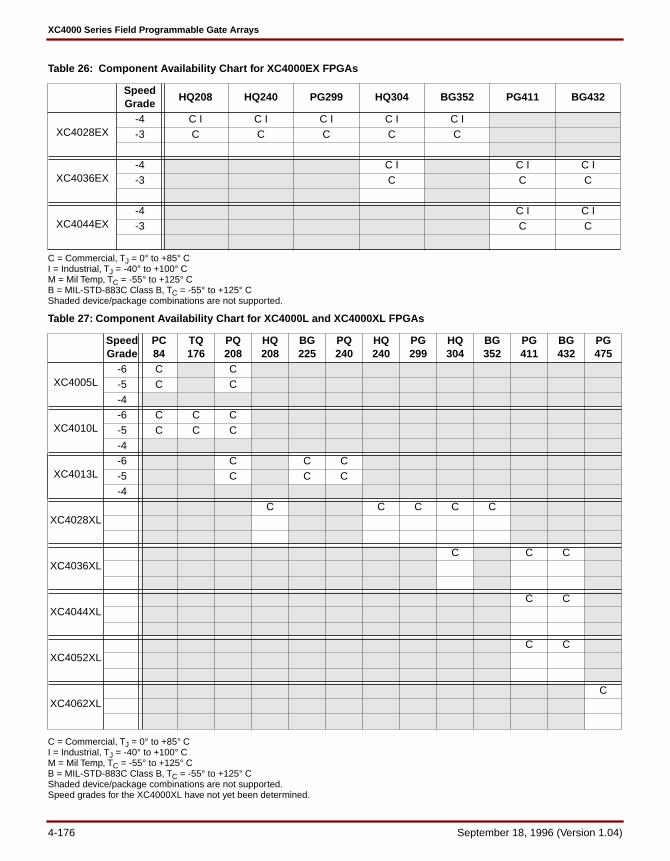
XC4000 Series Field Programmable Gate Arrays
C = Commercial, TJ = 0° to +85° C I = Industrial, TJ = -40° to +100° CM = Mil Temp, TC = -55° to +125° C B = MIL-STD-883C Class B, TC = -55° to +125° CShaded device/package combinations are not supported.
C = Commercial, TJ = 0° to +85° C I = Industrial, TJ = -40° to +100° CM = Mil Temp, TC = -55° to +125° C B = MIL-STD-883C Class B, TC = -55° to +125° CShaded device/package combinations are not supported.Speed grades for the XC4000XL have not yet been determined.
Table 26: Component Availability Chart for XC4000EX FPGAs
SpeedGrade
HQ208 HQ240 PG299 HQ304 BG352 PG411 BG432
XC4028EX-4 C I C I C I C I C I-3 C C C C C
XC4036EX-4 C I C I C I-3 C C C
XC4044EX-4 C I C I-3 C C
Table 27: Component Availability Chart for XC4000L and XC4000XL FPGAs
SpeedGrade
PC84
TQ176
PQ208
HQ208
BG225
PQ240
HQ240
PG299
HQ304
BG352
PG411
BG432
PG475
XC4005L-6 C C-5 C C-4
XC4010L-6 C C C-5 C C C-4
XC4013L-6 C C C-5 C C C-4
XC4028XLC C C C C
XC4036XLC C C
XC4044XLC C
XC4052XLC C
XC4062XLC
4-176 September 18, 1996 (Version 1.04)

User I/O Per PackageMaximum available user I/O for each device/package combination is shown in Table 28 - Table 30.
Pinout tables for XC4000-Series devices follow. Pinout data is offered in two forms, as device-specific and package-specifictables. Device-specific tables include all packages for each XC4000-Series device. They follow the pad locations aroundthe die, and include boundary scan register locations. Package-specific tables include all XC4000-Series devices availablein a given package. These tables are especially useful in determining which pads should be avoided, in case of a futuretransition to a different device in the same package.
All pinouts defined at the time of publication are included in these tables. Additional information may be available. Call yourlocal sales office or see the Xilinx WEBLINX at http://www.xilinx.com for the latest information.
Note: This table includes standard user-programmable I/O. It also includes the TDI, TCK, and TMS pins, which can function as user-programmable I/O if not used for boundary scan. In addition to the I/O listed in this table, the M0 and M2 pins can be used as inputs only; the M1 and TDO pins can be used as outputs only. All of these pins must be called out using special library symbols. The XACT software does not use them by default. (See Table 18 on page 47.)
Table 28: Maximum User I/O for XC4000E Device/Package Combinations
No. of Pins
Package (Code)
XC4003E XC4005E XC4006E XC4008E XC4010E XC4013E XC4020E XC4025E
Maximum User I/O 80 112 128 144 160 192 224 25684 PLCC (PC) 61 61 61 61 61
100 PQFP (PQ) 77 77VQFP (VQ) 77
120 PGA (PG) 80144 TQFP (TQ) 112 113156 PGA (PG) 112 125160 PQFP (PQ) 112 128 129 129 129164 CBFP (CB) 112191 PGA (PG) 144 160196 CBFP (CB) 160208 PQFP (PQ) 112 128 144 160 160
HQFP (HQ) 160 160 160223 PGA (PG) 192 192 192225 BGA (BG) 160 192228 CBFP (CB) 192 192240 PQFP (PQ) 192
HQFP (HQ) 192 192 193299 PGA (PG) 256304 HQFP (HQ) 256
September 18, 1996 (Version 1.04) 4-177

XC4000 Series Field Programmable Gate Arrays
Note: This table includes standard user-programmable I/O. It also includes the TDI, TCK, and TMS pins, which can function as user-programmable I/O if not used for boundary scan. In addition to the I/O listed in this table, the M0 and M2 pins can be used as inputs only; the M1 and TDO pins can be used as outputs only. All of these pins must be called out using special library symbols. The XACT software does not use them by default. (See Table 18 on page 47.)
Note: This table includes standard user-programmable I/O. It also includes the TDI, TCK, and TMS pins, which can function as user-programmable I/O if not used for boundary scan. In addition to the I/O listed in this table, the M0 and M2 pins can be used as inputs only; the M1 and TDO pins can be used as outputs only. All of these pins must be called out using special library symbols. The XACT software does not use them by default. (See Table 18 on page 47.)
Table 29: Maximum User I/O for XC4000EX Device/Package Combinations
No. of Pins Package (Code) XC4028EX XC4036EX XC4044EXMaximum User I/O 256 288 320
208 HQFP (HQ) 160240 HQFP (HQ) 193299 PGA (PG) 256304 HQFP (HQ) 256 256352 BGA (BG) 256411 PGA (PG) 288 320432 BGA (BG) 288 320
Table 30: Maximum User I/O for XC4000L and XC4000XL Device/Package Combinations
No. of Pins
Package (Code)
XC4005L XC4010L XC4013L XC4028XL XC4036XL XC4044XL XC4052XL XC4062XL
Maximum User I/O 112 160 192 256 288 320 352 38484 PLCC (PC) 61 61
176 TQFP (TQ) 153208 PQFP (PQ) 112 160 160208 HQFP (HQ) 160225 BGA (BG) 192240 PQFP (PQ) 192240 HQFP (HQ) 193299 PGA (PG) 256304 HQFP (HQ) 256 256352 BGA (BG) 256411 PGA (PG) 288 320 352432 BGA (BG) 288 320 352475 PGA (PG) 384
4-178 September 18, 1996 (Version 1.04)
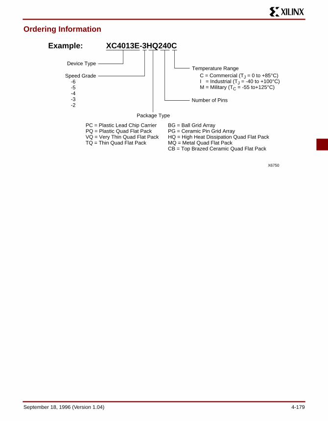
Ordering Information
XC4013E-3HQ240C
Device Type
Speed Grade -6 -5 -4 -3 -2
Number of Pins
Package Type
Temperature RangeC = Commercial (TJ = 0 to +85°C) I = Industrial (TJ = -40 to +100°C) M = Military (TC = -55 to+125°C)
PC = Plastic Lead Chip Carrier PQ = Plastic Quad Flat Pack VQ = Very Thin Quad Flat Pack TQ = Thin Quad Flat Pack
BG = Ball Grid Array PG = Ceramic Pin Grid Array HQ = High Heat Dissipation Quad Flat Pack MQ = Metal Quad Flat Pack CB = Top Brazed Ceramic Quad Flat Pack
X6750
Example:
September 18, 1996 (Version 1.04) 4-179
XC4000 Series Field Programmable Gate Arrays
4-180 September 18, 1996 (Version 1.04)