Xampling: Analog to Digital at Sub-Nyquist Rates
16
Department of Electrical Engineering Electronics Computers Communications Technion—Israel Institute of Technology Technion City, Haifa 32000, Israel, Tel: 972-4-8294680, Fax: 972-4-8295746, www.ee.technion.ac.il Xampling: Analog to Digital at Sub‐Nyquist Rates Moshe Mishali, Student Member, IEEE, and Yonina C. Eldar, Senior Member, IEEE, Oleg Dounaevsky and Eli Shoshan Abstract We present a sub-Nyquist analog-to-digital converter of wideband inputs. Our circuit realizes the recently proposed modulated wideband converter, which is a flexible platform for sampling signals according to their actual bandwidth occupation. The theoretical work enables, for example, a sub-Nyquist wideband receiver, which has no prior information on the transmitter carrier positions. Our design supports input signals with 2 GHz Nyquist rate and 120 MHz spectrum occupancy, with arbitrary transmission frequencies. The sampling rate is as low as 280 MHz. To the best of our knowledge, this is the first reported wideband hardware for sub- Nyquist conversion. Furthermore, the modular design is proven to compete with state-of-the-art Nyquist ADCs in terms of resolution bits and full-scale range. We describe the various circuit design considerations, with an emphasis on the nonordinary challenges the converter introduces: mixing a signal with a multiple set of sinusoids, rather than a single local oscillator, and generation of highly-transient periodic waveforms, with transient intervals on the order of the Nyquist rate. A series of hardware experiments validates the design and demonstrate sub-Nyquist sampling. CCIT Report No. 751, EE Pub No. 1708 December, 10 th 2009 Department of Electrical Engineering Technion – Israel Institute of Technology arXiv:0912.2495v1 [nlin.CG] 13 Dec 2009
Transcript of Xampling: Analog to Digital at Sub-Nyquist Rates
Department of Electr ical Engineering
Electron ics Computers Communicat ions Technion—Israel Inst i tute of Technology
Technion City, Hai fa 32000, Israel , Tel: 972-4-8294680, Fax: 972-4-8295746, www.ee.technion.ac.il
Xampling:
Analog to Digital at Sub‐Nyquist Rates
Moshe Mishali, Student Member, IEEE, and Yonina C. Eldar, Senior Member, IEEE, Oleg Dounaevsky and Eli Shoshan
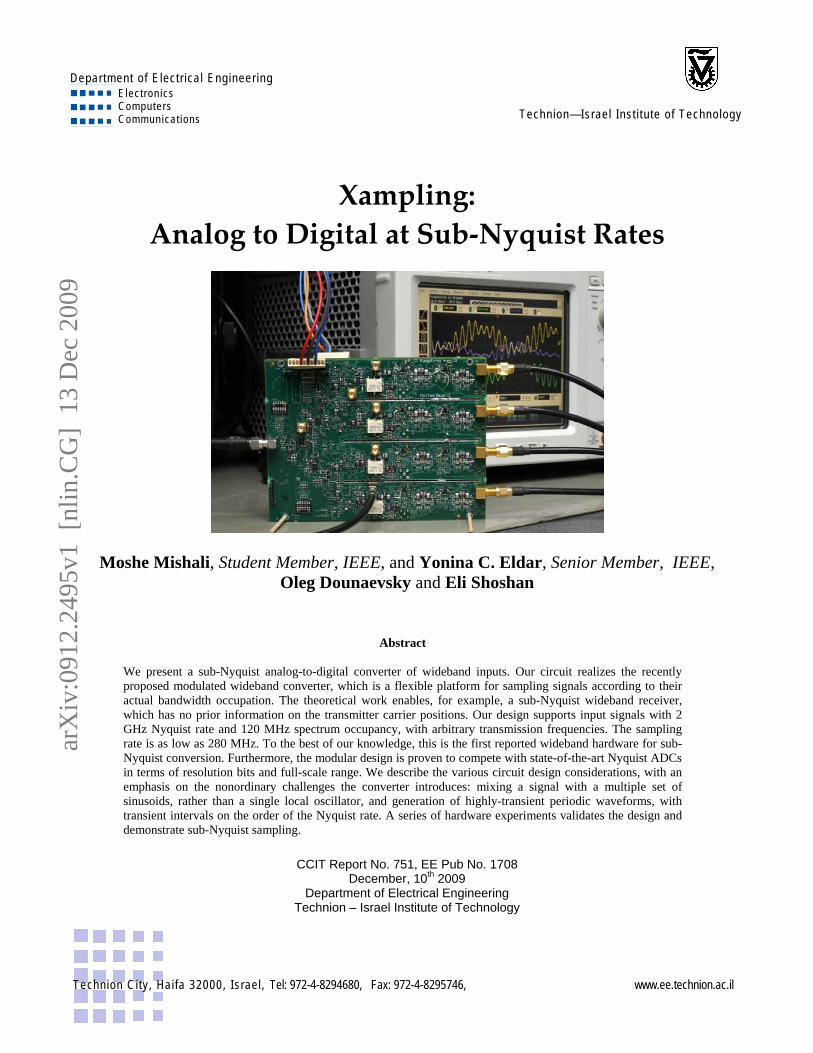
Abstract We present a sub-Nyquist analog-to-digital converter of wideband inputs. Our circuit realizes the recently proposed modulated wideband converter, which is a flexible platform for sampling signals according to their actual bandwidth occupation. The theoretical work enables, for example, a sub-Nyquist wideband receiver, which has no prior information on the transmitter carrier positions. Our design supports input signals with 2 GHz Nyquist rate and 120 MHz spectrum occupancy, with arbitrary transmission frequencies. The sampling rate is as low as 280 MHz. To the best of our knowledge, this is the first reported wideband hardware for sub-Nyquist conversion. Furthermore, the modular design is proven to compete with state-of-the-art Nyquist ADCs in terms of resolution bits and full-scale range. We describe the various circuit design considerations, with an emphasis on the nonordinary challenges the converter introduces: mixing a signal with a multiple set of sinusoids, rather than a single local oscillator, and generation of highly-transient periodic waveforms, with transient intervals on the order of the Nyquist rate. A series of hardware experiments validates the design and demonstrate sub-Nyquist sampling.
CCIT Report No. 751, EE Pub No. 1708
December, 10th 2009 Department of Electrical Engineering
Technion – Israel Institute of Technology
arX
iv:0
912.
2495
v1 [
nlin
.CG
] 1
3 D
ec 2
009

2
Xampling: Analog to Digital at Sub-Nyquist RatesMoshe Mishali, Student Member, IEEE, Yonina C. Eldar, Senior Member, IEEE, Oleg Dounaevsky and Eli
Shoshan
Abstract— We present a sub-Nyquist analog-to-digital con-verter of wideband inputs. Our circuit realizes the recentlyproposed modulated wideband converter, which is a flexibleplatform for sampling signals according to their actual bandwidthoccupation. The theoretical work enables, for example, a sub-Nyquist wideband receiver, which has no prior information on thetransmitter carrier positions. Our design supports input signalswith 2 GHz Nyquist rate and 120 MHz spectrum occupancy, witharbitrary transmission frequencies. The sampling rate is as low as280 MHz. To the best of our knowledge, this is the first reportedwideband hardware for sub-Nyquist conversion. Furthermore,the modular design is proven to compete with state-of-the-artNyquist ADCs in terms of resolution bits and full-scale range.We describe the various circuit design considerations, with anemphasis on the nonordinary challenges the converter introduces:mixing a signal with a multiple set of sinusoids, rather than asingle local oscillator, and generation of highly-transient periodicwaveforms, with transient intervals on the order of the Nyquistrate. A series of hardware experiments validates the design anddemonstrate sub-Nyquist sampling.
Index Terms— Analog to digital conversion, circuit implemen-tation, modulated wideband converter, sub-Nyquist sampling,Xampling.
I. INTRODUCTION
ANALOG to digital conversion (ADC) is the key enablingmany of the advances in signal processing. An ADC
device represents the continuous signal by a stream of numbersat finite resolution. Sophisticated software algorithms can thenbe used to manipulate the samples in order to achieve anydesired processing. The Shannon-Nyquist theorem [1], [2] liesat the heart of essentially all ADC devices. It states that signalbandlimited to B Hz can be perfectly recovered from uniformsamples, if the sampling rate is at least 2B samples/sec. Today,six decades after the formulation of this theorem by Shannon,there are various architectures for ADC design: flash, folding,pipelining, time-interleaving to name a few. However, theultimate goal remains Nyquist sampling, that is conversionat a rate which is twice the highest frequency of the input.
A survey and analysis of ADC technology was conducted adecade ago [3] and repeated in [4] several years ago. In Fig. 1,we map a database of more than 1200 ADC devices fromfour leading manufacturers, according to online datasheets[5]–[8]. The figure reproduces the inherent trade-off that waspreviously analyzed in [3], [4]: the faster the sampling rate thesmaller the number of bits that can be obtained. State-of-the-art Nyquist ADCs can achieve a sampling rate of 550 MHz
This work has been submitted to the IEEE for possible publication.Copyright may be transferred without notice, after which this version mayno longer be accessible.
The authors are with the Technion—Israel Institute of Technology, Haifa32000, Israel. Emails: [email protected], [email protected],[email protected], [email protected].
0
4
8
12
16
20
24
28
32
0 1 2 3 4 5 6 7 8 9 10 11 12Sampling rate (log10(samples/sec))
Stated number of bits
Analog Devices National Instruments Maxim Texas Instruments
State‐of‐the‐artNyquist ADCs
Fig. 1. Stated number of bits versus sampling rate. This paper demonstratessub-Nyquist sampling of 2 GHz Nyquist-rate signals occupying only a smallportion of the spectrum. The modular hardware can compete with state-of-the-art ADCs.
at 12 bits resolution [8], or 3 GHz with 8 bits resolution [6].The expected improvement trend is an increase of 1.5 bits atall sampling rates over a period of 8 years [3].
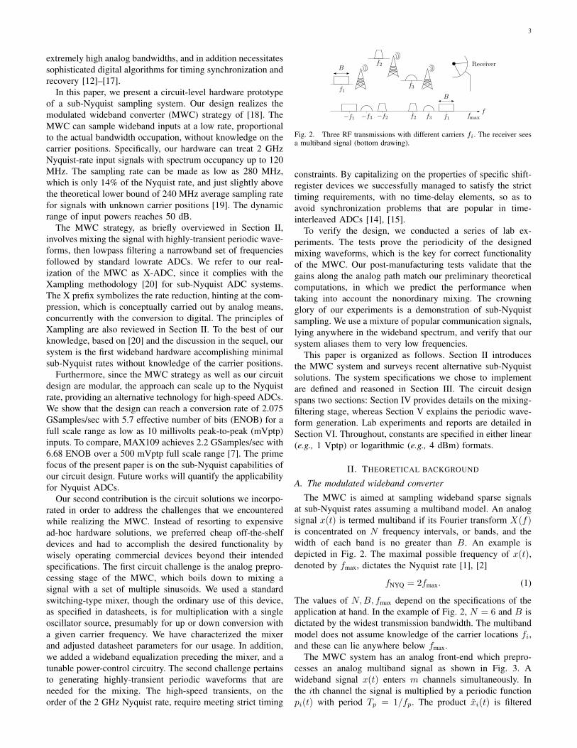
The improvement trend in state-of-the-art ADCs, based onthe reports [3], [4] and Fig. 1, is not sufficiently fast to catchup with the technology advances in related fields. For example:a prevalent scenario in communication is of a widebandreceiver, which intercepts a few narrowband transmissions,such that each information signal is modulated on a differentcarrier frequency, as depicted in Fig. 2. Nowadays, technologyenables modulating information on carrier frequencies aroundtens of GHz [9], far above the capabilities of existing ADCdevices.
The common practice in engineering to overcome the ADCbottleneck is demodulation, namely multiplying the input bythe carrier frequency fc of a band of interest, so as to shiftthe contents of the narrowband transmission from the highfrequencies to the origin. See [10] for common demodulationtopologies. Therefore, instead of direct sampling of a wide-band input, which may be impossible with existing technology,each band is treated individually. However, demodulationrequires knowing the exact carrier frequency. This knowledgepresumably requires user assistance, e.g., when tuning a radioto the frequency of a station of interest. Unfortunately, such auser-assisted solution is impractical in many applications, suchas military surveillance, radar, electronic warfare and medicalimaging. There is no time to scan for the unknown fc – thetarget may be moving and the patient cannot stand a lengthyradiation exposure. To-date, the alternative to demodulationis to sample the entire wideband spectrum, for example byusing a series of low-rate samplers through time interleav-ing [11]. This requires excessive hardware solutions with
3
extremely high analog bandwidths, and in addition necessitatessophisticated digital algorithms for timing synchronization andrecovery [12]–[17].
In this paper, we present a circuit-level hardware prototypeof a sub-Nyquist sampling system. Our design realizes themodulated wideband converter (MWC) strategy of [18]. TheMWC can sample wideband inputs at a low rate, proportionalto the actual bandwidth occupation, without knowledge on thecarrier positions. Specifically, our hardware can treat 2 GHzNyquist-rate input signals with spectrum occupancy up to 120MHz. The sampling rate can be made as low as 280 MHz,which is only 14% of the Nyquist rate, and just slightly abovethe theoretical lower bound of 240 MHz average sampling ratefor signals with unknown carrier positions [19]. The dynamicrange of input powers reaches 50 dB.
The MWC strategy, as briefly overviewed in Section II,involves mixing the signal with highly-transient periodic wave-forms, then lowpass filtering a narrowband set of frequenciesfollowed by standard lowrate ADCs. We refer to our real-ization of the MWC as X-ADC, since it complies with theXampling methodology [20] for sub-Nyquist ADC systems.The X prefix symbolizes the rate reduction, hinting at the com-pression, which is conceptually carried out by analog means,concurrently with the conversion to digital. The principles ofXampling are also reviewed in Section II. To the best of ourknowledge, based on [20] and the discussion in the sequel, oursystem is the first wideband hardware accomplishing minimalsub-Nyquist rates without knowledge of the carrier positions.
Furthermore, since the MWC strategy as well as our circuitdesign are modular, the approach can scale up to the Nyquistrate, providing an alternative technology for high-speed ADCs.We show that the design can reach a conversion rate of 2.075GSamples/sec with 5.7 effective number of bits (ENOB) for afull scale range as low as 10 millivolts peak-to-peak (mVptp)inputs. To compare, MAX109 achieves 2.2 GSamples/sec with6.68 ENOB over a 500 mVptp full scale range [7]. The primefocus of the present paper is on the sub-Nyquist capabilities ofour circuit design. Future works will quantify the applicabilityfor Nyquist ADCs.
Our second contribution is the circuit solutions we incorpo-rated in order to address the challenges that we encounteredwhile realizing the MWC. Instead of resorting to expensivead-hoc hardware solutions, we preferred cheap off-the-shelfdevices and had to accomplish the desired functionality bywisely operating commercial devices beyond their intendedspecifications. The first circuit challenge is the analog prepro-cessing stage of the MWC, which boils down to mixing asignal with a set of multiple sinusoids. We used a standardswitching-type mixer, though the ordinary use of this device,as specified in datasheets, is for multiplication with a singleoscillator source, presumably for up or down conversion witha given carrier frequency. We have characterized the mixerand adjusted datasheet parameters for our usage. In addition,we added a wideband equalization preceding the mixer, and atunable power-control circuitry. The second challenge pertainsto generating highly-transient periodic waveforms that areneeded for the mixing. The high-speed transients, on theorder of the 2 GHz Nyquist rate, require meeting strict timing
f1
Bf2
f3
f1
B
f2 f3
f−f1 −f2−f3
Receiver
fmax
Fig. 2. Three RF transmissions with different carriers fi. The receiver seesa multiband signal (bottom drawing).
constraints. By capitalizing on the properties of specific shift-register devices we successfully managed to satisfy the stricttiming requirements, with no time-delay elements, so as toavoid synchronization problems that are popular in time-interleaved ADCs [14], [15].
To verify the design, we conducted a series of lab ex-periments. The tests prove the periodicity of the designedmixing waveforms, which is the key for correct functionalityof the MWC. Our post-manufacturing tests validate that thegains along the analog path match our preliminary theoreticalcomputations, in which we predict the performance whentaking into account the nonordinary mixing. The crowningglory of our experiments is a demonstration of sub-Nyquistsampling. We use a mixture of popular communication signals,lying anywhere in the wideband spectrum, and verify that oursystem aliases them to very low frequencies.
This paper is organized as follows. Section II introducesthe MWC system and surveys recent alternative sub-Nyquistsolutions. The system specifications we chose to implementare defined and reasoned in Section III. The circuit designspans two sections: Section IV provides details on the mixing-filtering stage, whereas Section V explains the periodic wave-form generation. Lab experiments and reports are detailed inSection VI. Throughout, constants are specified in either linear(e.g., 1 Vptp) or logarithmic (e.g., 4 dBm) formats.
II. THEORETICAL BACKGROUND
A. The modulated wideband converter
The MWC is aimed at sampling wideband sparse signalsat sub-Nyquist rates assuming a multiband model. An analogsignal x(t) is termed multiband if its Fourier transform X(f)is concentrated on N frequency intervals, or bands, and thewidth of each band is no greater than B. An example isdepicted in Fig. 2. The maximal possible frequency of x(t),denoted by fmax, dictates the Nyquist rate [1], [2]
fNYQ = 2fmax. (1)
The values of N,B, fmax depend on the specifications of theapplication at hand. In the example of Fig. 2, N = 6 and B isdictated by the widest transmission bandwidth. The multibandmodel does not assume knowledge of the carrier locations fi,and these can lie anywhere below fmax.
The MWC system has an analog front-end which prepro-cesses an analog multiband signal as shown in Fig. 3. Awideband signal x(t) enters m channels simultaneously. Inthe ith channel the signal is multiplied by a periodic functionpi(t) with period Tp = 1/fp. The product xi(t) is filtered

4
yi[n]
h(t)
p1(t)
h(t)
pm(t)
x(t)
ym[n]
y1[n]
Lowpass t = nTs
Tp-periodic
1/Ts
pi(t)
xi(t)
xm(t)
x1(t)
RF front-end Lowrate ADC(Low analog bandwidth)
Fig. 3. The modulated wideband converter: a practical sampling stage formultiband signals.
by an ideal lowpass filter h(t) with cutoff fs/2, and thensampled uniformly every Ts = 1/fs seconds. In the basicconfiguration m ≥ 4N and fs = fp ≥ fNYQ/B [18]. Thesampling rate is 4NB which can be significantly smaller thanfNYQ. Reconstruction of the signal is obtained by appropriatedigital processing, as discussed in [18].
The mixing operation scrambles the spectrum of x(t), suchthat a portion of the energy of all bands appear in baseband.More specifically, since each pi(t) is periodic, it has a Fourierexpansion
pi(t) =∞∑
l=−∞
cilej 2πTp
lt. (2)
Therefore, the mixing results in a weighted-sum of fp-shiftedcopies of X(f), such that the weights are the Fourier coeffi-cients cil [18]. The lowpass filter h(t) transfers only the narrowband frequencies up to fs/2 from that mixture to the outputsequence yi[n]. The aliased output is illustrated in Fig. 4.Whilst aliasing is often an undesired artifact in sampling, hereit is deliberately utilized to generate mixtures at baseband.Intuitively, if pi(t) are wisely designed such that the sequencesyi[n] capture different combinations of the spectrum, then thesignal is determined from the samples in all branches.
Lowrate ADCs follow the RF front-end. Commercial de-vices can be used for that task due to the preceding lowpass.The fact that the ADCs see only a lowpass input is a majoradvantage with respect to time-interleaved ADCs, in whichthe lowrate ADCs necessitate specialized Nyquist-rate front-end since they are connected directly to the wideband input.The MWC shifts the Nyquist burden to the RF mixers, ratherthan imposing this complexity on the internal track-and-holdcircuitry of the ADC. The low analog bandwidth ADCs and thecheap RF mixers allows realizing the MWC at a low cost. Thedevelopments in [18], [20] provide the digital means to extractany information band of interest from the seemingly-corruptedsub-Nyquist sequences yi[n], or alternatively to recover the
f0 maxf
fp
lfp lfp lfp
+
cil
cil
cil
Spectrum of x(t)
Spectrum of yi[n] Spectrum of yi′ [n]
+
ci′l
ci′ l
ci′ l
Fig. 4. The spectrum slices from x(t) are overlayed in the spectrum of theoutput sequences yi[n]. In the example, channels i and i′ realize differentlinear combinations of the spectrum slices centered around lfp, lfp, lfp. Forsimplicity, the aliasing of the negative frequencies is not drawn.
original input x(t). Our prime goal in the present paper is tofocus on the hardware realization of the RF front-end in Fig. 3.
The choice of the periodic functions pi(t) dictates theNyquist rate of the input signals that the MWC can handle.In particular, if pi(t) has Fourier coefficients cil with non-negligible amplitudes for all 0 ≤ l ≤ L, then the MWC cancapture signals with band locations anywhere below Lfp, cor-responding to a Nyquist rate of 2Lfp. The precise requirementon the magnitude of cil depends on the properties of the digitalreconstruction algorithm and is beyond the current scope [18].Nonetheless, in principle, every periodic function with high-speed transitions within the period Tp can be appropriate. Onepossible choice for pi(t) is a sign-alternating function, with Msign intervals within the period Tp. The choice M ≈ fNYQ/Bwas proposed in [18] and analyzed in [21].
The basic MWC configuration, fs = fp ≈ fNYQ/B, issufficient for theoretical interest. In the realization of Fig. 3,we utilized two variants of the basic configuration, that wereproposed in [18] and have practical value. The MWC hasan advanced version in which fs = qfp for some integerq > 1. In this setting, the sampling rate of a single channel isq times higher than fp. This allows to reduce the requirednumber of channels by the same factor. Conceptually, theadvanced configuration collapses the m channels in Fig. 3at the expense of higher sampling rate per channel. Moderatevalues for q are preferred, since this option requires additionaldigital computations. Another variant of interest is sharing thehardware that generates pi(t). In [18], we used simulationsto show that the reconstruction performance is hardly affectedwhen generating several pi(t) from a single shift register (SR)of length M by using different taps.
B. Xampling and related works
Xampling is a design methodology for sub-Nyquist systemswhich we recently introduced in [20], [22]. The Xamplingframework aims at breaking through the Nyquist barrier by

5
exploiting the fact that many analog signals are structured,e.g., constructed from several narrow frequency bands, eventhough the carrier locations are unknown. Xampling requiresa sub-Nyquist solution to satisfy four basic principles: capturea broad set of analog inputs, low sampling rate, efficientimplementation and processing capability of any informationband of interest at a low rate.
In [20], we compared past and recent approaches in light ofthe four Xampling criteria. It was shown that the Achilles heelof pointwise strategies, such as classic nonuniform sampling,is the required analog bandwidth of the ADC which remainsat the Nyquist rate, regardless of the low average nonuni-form rate. The analog bandwidth limitation, which stemsfrom the speed of the ADC internal track-and-hold circuitry,holds for pointwise strategies when the carrier frequenciesare known [23]–[25] and even when utilized for the caseof unknown transmission locations [19]. The literature ofcompressed sensing [26], [27] describes the random demodu-lation approach [28], [29] which is based on discretization ofthe frequency axis. As discussed in [20], the discrete modelbecomes sensitive when attempting to represent continuoussignals, the solution involves severe computational loads andalso precludes processing at a low rate.
In the technology survey of [20], the MWC was foundsuperior – it has many advantages in a one-by-one comparisonwith past solutions, and the MWC is the only system to-date satisfying all four Xampling criteria. The present paperpromotes the premise of the MWC from theory to practice.
We point out two related hardware publications. The tech-nique of random demodulation underlying [28], [29] was in-troduced in [30], where the building blocks were simulated inHSPICE for synthetic inputs, matching the discretized modelof [28]. A hardware realization of the random demodulationhas been presented [31] for a 800 kHz Nyquist-rate input and100 kHz sampling rate. The digital reconstruction was carriedout by a 160 MHz processor. The Nyquist folding systemof [32], which was also surveyed in [20], was demonstratedto smear a pure sinusoid input signal into a lowrate phase-modulated output, where the input frequency can be inferredfrom the width of the output spectrum. The smearing effecton a narrowband transmission is more complicated, and theinference of the narrowband contents from the output wasnot considered in [32]. In contrast, the results we reporton in Section VI demonstrate accurate aliasing of popularcommunication signals from their (a-priori unknown) high-rate positions around hundreds of MHz to lowrate frequencies.The signal shape is unaltered, enabling the subsequent lowratedigital processing of [18], [20] to extract the underlyinginformation. To the best of our knowledge, this paper is thefirst to present a wideband hardware of a sub-Nyquist system.
III. PROTOTYPE ARCHITECTURE
The MWC is a flexible system with various parameters. Inthis section, we detail the specifications that we chose to real-ize and the main circuit challenges. Our guideline in selectingthe parameters was to accomplish a system which competeswith state-of-the-art ADCs, in terms of input bandwidth andresolution, while minimizing the hardware size and cost.
A. SpecificationsSystem scope. Our board prototype implements the RF
front-end of the MWC, from the input x(t) until the analogoutputs of the filters h(t). This scope captures the innovativetheoretical parts as well as the challenges in the actual design,which are explained in the sequel. The conversion to digitalof the lowpass filtered mixtures is immediately carried outusing commercial devices. In the experiments we used a four-channel scope for that purpose.
Input model. We consider a wideband multiband modelwith N = 6 bands, namely 3 concurrent transmissions, andmaximal bandwidth B = 19 MHz. These specifications wereused in the theoretical simulations of [18] and represent apossible wideband scenario for the proof of concept. TheNyquist rate fNYQ we consider is 2.075 GHz. In the prototype,this number stems from the frequency of a voltage-controlled-oscillator (VCO) we chose. Higher Nyquist rates are possiblefor higher VCO rates, though as fNYQ increases layout designbecomes a factor, beyond the proof of concept which we areinterested in here.
Periodicity. We set the time period Tp to the smallest valuesatisfying 1/Tp ≥ B subject to the additional considerationswhich are detailed hereafter.
Periodic waveforms. Sign alternating waveforms at thefNYQ speed are chosen, where theoretically a sign pattern oflength M ≥ dfNYQ/Be = 104 is needed [18]. In practice,M = 108 is used due to packaging considerations that areexplained in Section V. This value translates to an aliasingspacing fp = fNYQ/M = 19.212 MHz. To reduce thehardware size, we employed the idea of deriving all waveformsfrom different taps of a single SR of length-M . The sign valuesare programmable.
Filter cutoff. As part of the efforts to reduce hardware size,we choose the advanced MWC configuration, with q = 3. Inturn, the ideal filter cutoff would be qfp/2 = 28.5 MHz.In practice, the filter cutoff is not sharp and exceeds toaround 33 MHz. The nonideal filter response is calibrated aftermanufacturing [33].
Sampling rate (per channel). In the prototype, we samplethe filter outputs with a standard four-channel scope, thereforethe sampling rate fs is flexible and can approach twice thefilter cutoff, fs = 70 MHz. When sampling the outputswith ADC devices, the sampling rate fs should be chosenin accordance to the rates of available devices. As depictedin Fig. 1, there are many commercial ADC devices that cansuit the low bandwidth of the MWC outputs. For example: 80MSamples/sec at 16 bits resolution can be achieved by eitherAD9460 [5], MAX19586 [7], ADC14DS080 [6], or ADS5562[8].
Number of channels. Theoretically, we need m ≥ 4N =24 channels for the basic configuration, or m = 24/q = 8channels for the advanced one which we use here. In theprototype, we realized only m = 4 channels, since yi[n] areacquired by a standard four-channel scope. Compensating thefactor of two is accomplished by additional digital compu-tations [19]. The alternative design choice of q = 6 whichwould require m = 24/6 = 4 channels and fs ≈ 140 MHzwas avoided due to resolution aspects that are discussed below.

6
TABLE IPROTOTYPE PARAMETERS
Parameter Choice
Signal model N = 6, B = 19 MHz, fNYQ = 2 GHzNumber of channels m 4Waveform type periodic sign alternationAlternation rate 2.075 GHzSign pattern length M 108Period fp 2.075/108 = 19.212 MHzFilter cutoff 33 MHzSampling rate/channel fs 70 MHz
Since the system is modular, a future version can duplicatethe hardware and integrate a bank of 8 ADCs to eliminateadditional digital computations. We note that the theory ofmultiband sampling necessitates a minimal sampling rate of2NB = 228 MHz, regardless of the sampling architecture[19]. Our realization approaches the bound with 280 MHzsampling rate, that is about 14% of the Nyquist rate.
Resolution. Fig .1 shows that 16 bit resolution is customaryaround fs ≈ 70 MHz. In comparison, for q = 6 and fs ≈ 140MHz, 12 bit resolution is more popular. Since noise alwaysdegrades the effective number of bits, we choose 16 bits.
Circuit separation. The design is implemented using twophysical printed boards. An analog board realizes the fouranalog paths from x(t) to the relevant filter outputs, whereasa digital counterpart provides the periodic waveforms. Theseparation avoids possible digital noise from interfering withthe analog tasks. In addition, it allows for future designsto replace the sign alternation waveforms with any desiredperiodic function. Another advantage is the ability to verifyeach part of the design separately.
Table I summarizes the parameters for convenience.
B. Circuit challenges
In designing an analog circuit to realize the MWC weencountered two main show-stoppers: (I) analog mixing withspectrally-rich waveforms pi(t), and (II) constructing the pe-riodic waveforms with the required alternation speed of 2.075GHz. RF mixers are tailored for multiplication with a singlesinusoid, which is the standard procedure for modulating anddemodulating an information band onto a given carrier fc.In contrast, the MWC requires a simultaneous multiplicationwith many sinusoids – those comprising pi(t). This results inattenuation of the output and substantial nonlinear distortionnot accounted for in datasheet specifications. The next sectiondetails the design of the analog board, in which we includeda frequency equalizer and a tunable power control on pi(t), topartially account for the nonordinary mixing. Further researchcan assist in a broad investigation of mixing with multiplesinusoids, beyond the current application.
The second challenge pertains to constructing pi(t). Thewaveforms can be generated either by analog or digital means.Analog waveforms, such as sinusoid, square or sawtooth wave-forms, are smooth within the period, and therefore do not haveenough transients at high frequencies which is necessary to
ensure sufficient aliasing. On the other hand, digital waveformscan be programmed to any desired number of alternationswithin the period, but require meeting timing constraints on theorder of the clock period. In our setting, the clock interval of1/fNYQ = 480 picosecs leads to severe timing constraints thatare difficult to satisfy with existing digital devices. Section Velaborates on this challenge and the solution we selected torealize in hardware.
IV. ANALOG BOARD
A. Description
The analog board consists of three consecutive stages:splitting the input into four channels, mixing with the signpatterns pi(t) and lowpass filtering. Fig. 5 presents a blockdiagram of the analog path end-to-end.
The input signal passes through a 100 MHz highpass filterin order to reject the range of radio stations and airporttransmissions, which are typically not of interest. A breakdowndiode is used to protect the circuit in case of instantaneoushigh input power. As common in RF paths, a low-noiseamplifier (LNA) leads a chain of analog amplifications. Weplaced several attenuators along the path, whose power losscan be digitally-controlled between 0 dB to -15.5 dB. Thesedevices allow to widen the dynamic range of the system asexplained in the next section. We point out that the actualsplit to four channels is carried out by splitting the signaltwice. This implementation is also reasoned by dynamic rangeconsiderations. RF switches are the last components in thesplitting stage. The switches allow shutting down any of thefour channels, while isolating it from the active branches, soas to avoid possible RF reflections.
Four identical blocks follow. In each block, the signal isequalized and then mixed with the corresponding waveformpi(t) which is provided by the digital board. The mixing stage– the heart of the MWC system – is explained in Section IV-C.An amplifier mitigates possible drips of the periodic waveforminto the rest of the signal path. A two-stage lowpass filteringconcludes the analog path. The next subsections explain thecircuit considerations underlying the structure of Fig. 5.
B. Link budget analysis
In realizing our sub-Nyquist system, we bared in mind therepresentative application of a wideband receiver of Fig. 2,which intercepts several communication transmissions, ap-pearing somewhere in a wideband spectrum. Communicationsignals often suffer high attenuations while in air, so thatwhen an RF antenna intercepts the signal, the power level istypically substantially lower than the amplitude levels neededfor sampling with either an ADC device or scope. CommercialADCs at rates around fs = 70 MHz can work with amplitudelevels as low as tens to hundreds of millivolts [5]–[8]. Wedecided to target an output amplitude of at least 250 millivoltspeak-to-peak (mVptp). Equivalently, we require an outputpower
Poutreq. ≥ −8.06 dBm. (3)

7
HPF100 MHz
InputGain = 13 dB
NF = 1 dBIP3 = 48 dB
VariableAttenuator
RF switch
Passivesplitter
LNA
-0.5 dB0 ÷ -16 dB
-6 dB
* *
**
Gain = 14 dBNF = 4 dB
IP3 = 27 dB
-1 dB
Equalizer
From Digital board
LPF10 MHz
LPF10 MHz
Adjustable Gain
Passive Mixer
LO
RF IFOP-AMP
Gain = 19 dBNF = 4 dB
IP3 = 37 dBGain = -16 dB
(see text)
-1 dB
20 dBm
Gain = 9 dBNF = 6 dB
IP3 = 42 dB
Gain = 8 dBNF = 6 dB
IP3 = 42 dB
OP-AMPAMPOut+
PassiveNetwork
Single-ended / Double-Balanced
Configurations
Out-
4 Instances
Split 1 to 4 Mixing Filtering
Requirements:
250 mVptp amplitude
15 dB SNDR
-0.5 dB
Fig. 5. A block diagram of the analog board.
Throughout, units are exchanged according to
Vrms =Vptp√
8, Power = 10 log10
(Vrms2
Z
), (4)
assuming the standard Z = 50 ohm network impedance,and that 1 dBm corresponds to 1 milliwatt. In addition, itis important to maintain a sufficiently high signal to noiseratio (SNR) so that the consecutive digital algorithms canfunction properly. Reconstruction in the presence of noise wasdemonstrated in [18], where it was shown that an SNR ofabout 15 dB allows correct recovery of the spectrum support,an essential operation preceding any further processing. Sincemixing is a nonlinear procedure, the output usually containsundesired spurious distorted images of the signal, which arealso considered as noise. Therefore,
SNDRreq. ≥ 15 dB (5)
stands for the required signal to noise-and-distortion ratio atthe filter outputs.
Link budget calculation is a common RF analysis in orderto predict the amplitude level and SNDR of an RF chain,such as Fig. 5. The analysis takes into account the gain, noisefigure (NF) and third intersection-point (IP3) of each of thedevices along the path. In what follows, we analyze the chainof devices in our realization with emphasis on design con-siderations due to the wideband nature of the front-end. Thecalculations also take into account the nonordinary mixing.The experiments in Section VI validate that the manufacturedboard indeed satisfies the requirements (3) and (5).
The amplitude requirement (3) boils down to minimal inputpower
PIN ≥ Poutreq. −∑
Gi = −8.06− 47 = −55 dBm, (6)
where the gains Gi are reported in Fig. 5, and the equalityabove is achieved when the attenuators are set to 0 dB.
To conduct an SNDR analysis we consider two extremescenarios. One of x(t) with a very low power, in which casethe SNDR is dictated mainly by the additional noise thatthe system generates. Technically, the noise figures and thegains of the devices along the path dictate this contribution.The other scenario assumes several narrowband transmissions,whose total power is high and is equally distributed. In thissetting, spurious images of the true signal appear due to the
nonlinearities of the devices. Since the input power is high,these images become dominant and distort the ability of thesystem to distinguish between the true input and the undesiredproducts. In a wideband system, the effect of nonlinearitiesis prominent since besides the undesired products that appearclose to the original frequencies, there are many other spuriousimages which fall well within the wideband range of the front-end.
Consider the case of x(t) with low power. The thermal noiseat the input of the system is
nthermal = KTW = −114+10 log10W = −80.82 dBm, (7)
where KT = −114 dBm is the thermal noise power per mega-Hz, and W = 2075 MHz is the intended frontend bandwidth.It follows from Frii’s formula [34]
Fsystem =SNRin
SNRout= F1 +
F2 − 1G1
+F3 − 1G1G2
+ · · · , (8)
that the equivalent noise figure of the system is Fsystem =3.13 dB. Consequently, the signal power at the input mustsatisfy
PIN,min ≥ SNDRreq. + nthermal + Fsystem = −62.5 dBm, (9)
which is implied by (6).To analyze the other extreme of high input power, the
attenuators are set to their maximal level of −15.5 dB in orderto deliberately reduce the aggregated gain, and thus decreasethe nonlinear effects. The contribution of the thermal noise forhigh input powers can be neglected. To derive the distortionlevel in this setting, we begin with the output signal power
Pout = NmaxGtotalPIN,max, (10)
where Nmax = 10 is taken for the maximal number of con-current narrowband transmissions that the system is designedfor. Note that Nmax is greater than the 3 transmissions takenin our signal model, since the system is modular and wewould like the design to support future applications withsignal sets beyond the specifications of Table I. The total gainGtotal =
∑Gi = 15 dB is calculated from Fig. 5, and PIN,max
is the unknown to be computed. We calculate the equivalentintercept point of the third order (IP3) of the entire system,

8
−80 −60 −40 −20 0−20
−10
0
10
20
30
40
50
Input power (dBm)
SN
DR
(d
B)
−30
−20
−10
0
10
20
30
40
Ou
tpu
t le
ve
l (d
Bm
)
Thermal−noisedominates
Distortionsdominate
Req. SNDR
Req. Amp
Dynamic range
(a)
−80 −60 −40 −20 0
−16
−14
−12
−10
−8
−6
−4
−2
0
Input power (dBm)
Att
enua
tor
level (d
B)
Attenuator #1
Attenuator #2
(b)
Fig. 6. The output power level and the SNDR are plotted in (a) for varyinginput power (solid lines), where the former is monotone in the input power.The dynamic range of the system is achieved when both requirements aresatisfied. The optimal attenuator levels (in the SNDR sense) are drawn in (b).
using the formula [35]
(IP3system)−1 =I∑
i=1
IP3i
I∏j=i+1
Gj
−1
= (30.98 dBm)−1,
(11)where I = 15 is the number of RF devices in the path. Then,the SNDR at the output is given by [36]
SNDR = 2 (IP3system − Pout)− 7.3 dB. (12)
We subtract 7.3 dB in order to account for the fact that IP3measures the mutual distortion in the presence of two tonesonly. Compensating the equation for a larger number of inputtransmissions, Nmax = 10, requires this term [36]. Taking intoaccount the number of concurrent transmissions is extremelyimportant in a wideband system whose frequency bandwidthcovers more than an octave. In narrowband systems, variousintermodulations between any two input tones fall beyond theinput bandwidth. The distortions are rejected by the systemfilters and thus the number of transmissions hardly affect theSNDR. In contrast, intermodulations in a wideband system fallwithin the input bandwidth, modulates with the other tones,and thus raises the total distortion level. We conclude that thesignal input power must satisfy
PIN,max ≤IP3system −12(SNDRreq. + 7.3) (13)
− 10 log10Nmax −Gtotal = −5.17 dBm.
Our system can therefore treat input signals at a dynamicrange of 49 dB, as follows from (6), (9) and (13). We note thatthe calculations of the distortion level for high-power signalsassume that all narrowband transmissions have equal powers.Refining the theoretical calculations for different power levelsis possible. However, since the link budget analysis has spareswe did not pursue this direction; Section VI reports on anactual 50 dB dynamic range of the manufactured system.Fig. 6 depicts the output level and the SNDR for varyinginput power, when optimizing for the highest SNDR over allpossible attenuator levels using (9) and (13). We point out thatthe increase in the attenuators level does not breach (3) for allinput power higher than -55 dBm.
We also considered an alternative design in which the signalis split into four channels immediately after the first attenuator,with no additional splitting at the end. Repeating the link
budget analysis shows that the dynamic range due to the SNDRrequirement, namely the difference between (9) and (13),would have been narrowed by 4 dB, or equivalently a factorof 2.5 in the range of allowed peak-to-peak input amplitudes.When taking into account the amplitude requirement thedynamic range is narrowed by only 1 dB. Nonetheless, weavoided this option in order to improve the SNDR in case (3)is relaxed in a future system. Another reason is that a directsplitting system would require an additional four amplifiersand two digital attenuators.
Fig. 6 can be used to study the potential of the X-ADCarchitecture as an alternative to existing Nyquist ADCs whenusing m branches such that mfs ≥ fNYQ. Specifically,Fig. 6(a) predicts a maximal SNDR level of 42 dB, whichis achieved for an input power of -25 dBm. In practice, theexperiments in Section VI-B affirm a maximal SNDR of 36.2dB at -35 dBm input power. In ADC terminology, the ENOBof our system is [37]
ENOB = (SNDR− 1.76)/6.02 = 5.7 bits, (14)
for a full-scale range of 10 mVptp. Since the MWC designis modular and can scale up to the Nyquist rate, in principle,the system can reach a sampling rate of 2.075 GSamples/secwith the above specifications.
C. Mixing with multiple sinusoids
The mixing stage is a major circuit challenge in realizing theMWC. A standard switching-type mixer has three ports: RF,local oscillator (LO) and intermediate frequency (IF), hintingat the common usage – multiplication of an RF signal by asingle sinusoid. In contrast, the MWC requires the nonordinarymixture x(t)pi(t), that is with the multiple sinusoids com-prising pi(t). The immediate consequence of this nonordinarymixing is a choice of passive device. Active mixers, namelythose with external power supply, typically have a narrowinput bandwidth which is not suited for wideband sampling.The passive mixer device in our system (SYM25-DHW) isspecified for RF inputs from DC to 6 GHz. The datasheetsalso allow LO frequency between 80 MHz and 2.5 GHz,referring to a single oscillation source. There are severalother impacts on the RF path due to the nonordinary mixingof the MWC. First, in the calculations of the link budgetbefore, we had to adjust the mixer parameters (gain, noisefigure and IP3) since conventional datasheets characterize thedevice only for multiplication with a single LO source. Thesemodifications impacted the hardware design as the actualgain of the system is less than expected from datasheets andadditional amplifications were required. Second, we insertedan adjustable power control on the energy of pi(t) close to theLO port of the mixer. The third circuit is a wideband equalizerwhich we located nearby the RF port. These modifications arehighlighted in Fig. 7 and are next explained.
Link budget analysis is based on datasheet specifications(gain, noise figure and IP3). When mixing with multiplesinusoids, interpreting the device specifications become cum-bersome. For example: a passive mixer requires a minimal LOpower to bias the circuit; 17 dBm in the case of the device

9
1
1
2
2
3
3
4
4
5
5
6
6
7
7
8
8
D D
C C
B B
A A
Title
Number RevisionSize
A3
Date: 06/12/2009 Sheet ofFile: D:\Projects\moshiko\mixing.SchDoc Drawn By:
82pFC18
18pF
C10NCL7
0R
C6
1nF
C8
100pF
C2
18pF
C4
1nF
C1
1nF
C9
18R
R9
300RR10
300RR11
VCC9V
1k
R3
10k
R4
VCC9V
10k
R8
ncR13
ncR12
2N3904Q6
2N3906
Q5
2N3906Q7
2N3904Q8CTRL_UP
CTRL_UP
1k
R7
1
2
3
4
GALI-84
GND
GND
IN OUT
gain: 20db
P1db: 21dBm
U2
RF1
2
IF 3
4 5 6 SYM25-DHWGND
LO
conv. loss: 6db
U3
1
2
3
4
GALI-84
GND
GND
IN OUT
gain: 18dbP1db: 23dBm
U1
62RR5
62RR6
62RR1
62RR2
330nHL1
330nHL2
MCX
J1
SMA
J3
SMAJ4
100pF 100pF
C17
100nHL6
100nHL8
1nF
C3
100pF
C5
120nH
L10
120nH
L15
12nH
4.7nH
0.8pF
1.5pF
30
90
30
In Out
Adjusted: 16 db
Passive mixer
Adjustable LO power
Wideband equalizer
P0C101 P0C102
P0C201 P0C202
P0C301 P0C302
P0C401 P0C402
P0C501 P0C502
P0C601 P0C602 P0C801 P0C802 P0C901 P0C902
P0C1001 P0C1002
P0C1101 P0C1102
P0C1601 P0C1602 P0C1701 P0C1702
P0C1801
P0C1802
P0C1901 P0C1902
P0J101
P0J102
P0J103
P0J104
P0J105
P0J301
P0J302
P0J303
P0J304
P0J305
P0J401
P0J402
P0J403 P0J404
P0J405
P0L101
P0L102
P0L201
P0L202
P0L601
P0L602
P0L701
P0L702
P0L801
P0L802
P0L901 P0L902
P0L1001 P0L1002 P0L1501 P0L1502
P0L1601 P0L1602
P0Q501
P0Q502
P0Q503
P0Q601
P0Q602
P0Q603
P0Q701
P0Q702
P0Q703
P0Q801
P0Q802
P0Q803
P0R101
P0R102
P0R201
P0R202
P0R301 P0R302
P0R401 P0R402
P0R501
P0R502
P0R601
P0R602 P0R701 P0R702
P0R801 P0R802
P0R901 P0R902
P0R1001
P0R1002
P0R1101
P0R1102
P0R1201
P0R1202
P0R1301
P0R1302
P0R1601 P0R1602 P0R1701 P0R1702
P0R1801
P0R1802
P0U101
P0U102
P0U103
P0U104
P0U201
P0U202
P0U203
P0U204
P0U301
P0U302
P0U303
P0U304
P0U305
P0U306
P0R401
P0R801 N0CTRL0UP
N0CTRL0UP
P0C102
P0C202
P0C302
P0C402
P0C502
P0C1002
P0C1802
P0C1901
P0J102
P0J103
P0J104
P0J105
P0J302
P0J303
P0J402
P0J403 P0J404
P0J405
P0L702
P0L1602
P0Q601
P0Q801
P0R1002
P0R1102
P0U102
P0U104
P0U202
P0U204
P0U304
P0U305
P0U306
P0C1101
P0R1601
P0C101 P0Q503
P0R101
P0R201
P0C201
P0L101
P0R102
P0R202
P0C301 P0Q703
P0R501
P0R601
P0C401
P0L102
P0L201
P0C501
P0L601
P0R502
P0R602
P0C601 P0R902
P0R1101
P0C602 P0C801
P0L701
P0C802 P0U101
P0C901
P0L202
P0U103
P0C902
P0U302
P0C1001
P0L602
P0L801
P0C1102 P0L902
P0C1601
P0L901
P0R1702
P0C1602 P0U201
P0C1701
P0L802
P0U203
P0C1702
P0R1202
P0U301
P0C1801
P0L1001 P0L1502
P0C1902 P0L1601
P0R1802
P0J101 P0R901
P0R1001
P0J301
P0R1201
P0J304
P0J305
P0J401
P0R1301
P0L1002
P0R1302
P0U303
P0Q502
P0R302
P0Q602 P0R402
P0Q603
P0R301
P0Q702
P0R701
P0Q802 P0R802
P0Q803
P0R702
P0R1602 P0R1701
P0R1801
P0L1501
P0Q501
P0Q701
N0CTRL0UP
P0R401
P0R801
P0C102
P0C202
P0C302
P0C402
P0C502
P0C1002
P0C1802
P0C1901
P0J102
P0J103
P0J104
P0J105
P0J302
P0J303
P0J402
P0J403 P0J404
P0J405
P0L702
P0L1602
P0Q601
P0Q801
P0R1002
P0R1102
P0U102
P0U104
P0U202
P0U204
P0U304
P0U305
P0U306
P0C1101
P0R1601
P0C101 P0Q503
P0R101
P0R201
P0C201
P0L101
P0R102
P0R202
P0C301 P0Q703
P0R501
P0R601
P0C401
P0L102
P0L201
P0C501
P0L601
P0R502
P0R602
P0C601 P0R902
P0R1101
P0C602 P0C801
P0L701
P0C802 P0U101
P0C901
P0L202
P0U103
P0C902
P0U302
P0C1001
P0L602
P0L801
P0C1102 P0L902
P0C1601
P0L901
P0R1702
P0C1602 P0U201
P0C1701
P0L802
P0U203
P0C1702
P0R1202
P0U301
P0C1801
P0L1001 P0L1502
P0C1902 P0L1601
P0R1802
P0J101 P0R901
P0R1001
P0J301
P0R1201
P0J304
P0J305
P0J401
P0R1301
P0L1002
P0R1302
P0U303
P0Q502
P0R302
P0Q602 P0R402
P0Q603
P0R301
P0Q702
P0R701
P0Q802 P0R802
P0Q803
P0R702
P0R1602 P0R1701
P0R1801
P0L1501
P0Q501
P0Q701
Fig. 7. The schematic of the mixing stage highlights three impacts of the nonordinary mixing with multiple sinusoids: a wideband equalizer preceding themixer, a tunable power control on LO port and a passive-type mixer. The datasheet specifications of the mixer were modified as explained in the text.
we chose. Here, this datum raises an interesting question:how should the LO power be set when its power is dividedbetween the various frequencies consisting pi(t). A naıveapproach would be to allocate a power of 17 dBm perharmonic, expecting a linear superposition behavior at theoutput. However, the mixer is a nonlinear device and the hugetotal power of that strategy would probably damage the device.On the other hand, allocating a total power of 17 dBm, willresult in each harmonic receiving significantly lower energypower.
In order to estimate the correct mixer parameters for theMWC setting, we performed experiments, similar to thoseconducted by the manufacturer, to characterize the conversionloss and the effective IP3 under a representative scenario ofmixing with multiple sinusoids. We concluded that the mixerparameters should be set to conversion loss of -16 dB, IP3 of27 dBm, and LO power of 20 dBm, instead of the datasheetspecifications of -6 dB, 30 dBm, and 17 dBm, respectively.Since the experiments were conducted before manufacturingwe also added an adjustable power control on the LO port ofeach mixer. In Section VI, these modifications are validatedon the manufactured board. We point out that RF simulationsoftwares, e.g., SPICE or ADS, cannot accurately model thenonordinary mixing, since manufacturers provide model filesonly for the conventional usage.
Moving on to the wideband equalizer. The purpose of anequalizer is to flatten the frequency response of the preced-ing stages. In selecting the equalizer, we had to make twouncommon choices due to the nonordinary mixing. The firstregards positioning the circuit in the middle of the RF chain,just before the mixer, instead of the common knowhow ofequalization towards the end of the chain, near the ADCterminals or even in the digital domain, where it can flattenthe response of the entire analog path. A passive equalization,rather than an active one (i.e., a circuit involving an operationalamplifier), is the second choice. This selection may seemcounterintuitive, since the insertion loss of a passive equalizeris high, especially since we located the equalizer in the middleof the RF chain, where the signal power is still moderate.
0.00 0.50 1.00 1.50 2.000.00
10.00
20.00
30.00
40.00
50.00
-10.00
-6.00
-2.00
2.00
6.00
10.00
F [GHz]
Freq
uenc
y R
espo
nse
(dB
)
Equa
lizer
Gai
n (d
B)
Ansoft CorporationXY Plot 1Circuit1
02 Jul 2009 14:58:49
Without Equalizer
Equalizer
With Equalizer
Y1dB(S21)NWA1
Y1dB(S43)NWA1
Y2dB(S65)NWA1
Fig. 8. The wideband equalizer flattens the frequency response at theRF port of the mixer. Low frequencies (up to 500 MHz) are attenuatedby approximately 8 dB, whereas high frequencies (above 1.5 GHz) are notaltered.
To explain both choices, we first recall how equalization isdesigned in conventional settings, that is when x(t) is mixedby a single sinusoid fc. RF devices attenuate the signal as itpasses through, where the attenuation is frequency-dependentand tends to increase at high frequencies. The goal of theequalizer is to correct the aggregated attenuation. The designrequires computing the frequency response from input to theequalizer, which as mentioned, is typically located at the endof the RF chain. Due to the frequency conversion by fc,the responses of the devices preceding the mixer need to betranslated by fc at the output of the mixer. The product ofthe responses along the path gives the aggregated attenuation,which the equalizer design fixes by adding gain or attenuationwhere needed, until the combined response is flattened.
In our sub-Nyquist system, the product x(t)pi(t) contains aweighed-sum of fp-wide spectrum slices of x(t); see Fig. 4.In particular, the output contains overlayed energy from theentire signal spectrum. Consequently, there is no simple wayto translate the frequency response of the devices precedingthe mixer to an equivalent response at the output. An analogequalizer, if located after the mixer, cannot be designed toflatten the response of the weighed-sum in yi[n]. A trickydigital equalization is possible, though at the expense of

10
high computational loads. This explains why we placed theequalizer circuit before the mixer. Compensating for the restof the path, namely for the nonideal response of the filterh(t), is done digitally [33]. The choice of passive equalizingis another consequence of the product x(t)pi(t). An activestage, which involves amplifiers, is typically limited in thefrequency range that can be corrected. In our setting, theequalizer is located before the mixer, at a point that a widebandresponse should be fixed. In addition, an active mixer cangenerate nonlinear effects and we preferred to avoid addingthose to the nonordinary mixture. To conclude, Fig. 8 displaysa simulation report from the board input to the RF port of themixer, ensuring an equalized flat response over the widebandregime until 2 GHz.
D. Lowpass filtering of spectrum mixtures
The filtering is the last processing step in the analog domain.The design focus here, which also stems from the nonordinarymixing, is on sharp transition around the cutoff and highattenuation in the stopband, namely for the frequency rangebeyond the cutoff. A nonflat response in the passband is not anissue, as it can be compensated digitally [33]. In typical RFchains, the stopband contains mainly noise, which the filterneeds to reject. Since the noise is anyway smaller in magnitudethan the in-band signal level, moderate attenuation is sufficient.In contrast, the MWC is based on deliberately introducingaliasing of the signal power over the entire wideband range.Therefore, the filter is required to isolate a specific workingband [−fs/2,+fs/2], while adjacent frequencies contain non-negligible energy due to other aliasing and must be effectivelyeliminated.
To achieve the high attenuation in the stopband, we havedesigned an elliptic filter of order seven as appears in Fig. 9.We used this filter twice with a buffering stage, as depictedin Fig. 5, in order to double the attenuation in the stopband.Fig. 10 presents a simulation report of the two-stage response,where we tuned the optimizer for a smooth transfer response,as measured by the curve of the S21 parameter. We avoideda single higher-order filter due to the following reason. TheS-parameters of a passive network satisfy |S21|2 + |S11|2 = 1.The simulation report implies that the optimal S21 is achievedat the expense of an oscillatory trend in the reflection param-eter S11. In practice, a physical network of passive elementsis likely to exhibit a smooth response for S11 as well, whichin turn means that it will be difficult to obtain the optimalS21. The oscillations in S11 increase with the filter order.Adding to that the fact that passive elements have tolerances,which cannot be accurately modeled in simulation, led us tothe design of two short-length stages.
The filter design is flexible and allows cutoff frequenciesup to 100 MHz by re-optimizing the values in Fig. 9. Inaddition, the design supports both single-ended and double-balanced output configurations. For verification with a scope,the single-ended version is used as it matches the scope front-end. Future applications can interface our board to commercialADCs, where balanced outputs may be preferred due to theirincreased immunity to noise.
1
1
2
2
3
3
4
4
5
5
6
6
7
7
8
8
D D
C C
B B
A A
Title
Number RevisionSize
A3
Date: 01/12/2009 Sheet ofFile: D:\Projects\moshiko\test2.SchDoc Drawn By:
IF1
82pFC56
18pF
C57
NCL20
0R
C51
1nF
C52
100pF
C49
18pF
C50
1nF
C48
1nF
C53
18R
R67
300RR68
300RR69
VCC9V
1k
R65
10k
R66
VCC9V
10k
R76
ncR75
ncR74
2N3904Q2
2N3906Q1
2N3906Q3
2N3904Q4CH1_CTRL_UP
CH1_CTRL_UP
1k
R72
1
2
3
4
GALI-84
GND
GND
IN OUT
gain: 20db
P1db: 21dBm
U18
RF1
2
IF 3
4 5 6 SYM25-DHWGND
LO
conv. loss: 6db
U17
1
2
3
4
GALI-84
GND
GND
IN OUT
gain: 18db
P1db: 23dBm
U16
62RR70
62RR71
62RR63
62RR64
330nHL18
330nHL19
MCX
J8
SMAJ9
SMAJ10
100pF
C459
100pF
C460
100nHL423
100nHL424
1nF
C454
100pF
C455
120nH
L21
120nH
L22
120pFC136
120pFC138
39pFC140
33pFC132
ncC147
33pFC135
ncC143
180pFC133100pFC131
ncC142
3.3pFC141
18pFC139
22pFC137
ncC134
ncC130ncC129ncC128
ncC148
ncC144
ncC149
330nH
L57
ncL59
150nH
L56
nc
L60
100nH
L58
nc
L61
0RR250
0RR251
0RR263
0RR264
In+
In-
Out+
Out-
P0C4801 P0C4802
P0C4901 P0C4902
P0C5001 P0C5002
P0C5101 P0C5102 P0C5201 P0C5202 P0C5301 P0C5302
P0C5601
P0C5602
P0C5701 P0C5702
P0C12801 P0C12802 P0C12901 P0C12902 P0C13001 P0C13002
P0C13101 P0C13102 P0C13201 P0C13202 P0C13301 P0C13302
P0C13401
P0C13402
P0C13501
P0C13502
P0C13601
P0C13602
P0C13701
P0C13702
P0C13801
P0C13802
P0C13901
P0C13902
P0C14001
P0C14002
P0C14101
P0C14102
P0C14201 P0C14202 P0C14301 P0C14302 P0C14401 P0C14402
P0C14701 P0C14702 P0C14801 P0C14802 P0C14901 P0C14902
P0C45401 P0C45402
P0C45501 P0C45502
P0C45901 P0C45902 P0C46001 P0C46002
P0J801
P0J802
P0J803
P0J804
P0J805
P0J901
P0J902
P0J903
P0J904
P0J905
P0J1001
P0J1002
P0J1003 P0J1004
P0J1005
P0L1801
P0L1802
P0L1901
P0L1902
P0L2001
P0L2002
P0L2101 P0L2102 P0L2201 P0L2202
P0L5601 P0L5602 P0L5701 P0L5702 P0L5801 P0L5802
P0L5901 P0L5902 P0L6001 P0L6002 P0L6101 P0L6102
P0L42301
P0L42302
P0L42401
P0L42402
P0Q101
P0Q102
P0Q103
P0Q201
P0Q202
P0Q203
P0Q301
P0Q302
P0Q303
P0Q401
P0Q402
P0Q403
P0R6301
P0R6302
P0R6401
P0R6402
P0R6501 P0R6502
P0R6601 P0R6602
P0R6701 P0R6702
P0R6801
P0R6802
P0R6901
P0R6902
P0R7001
P0R7002
P0R7101
P0R7102 P0R7201 P0R7202
P0R7401
P0R7402
P0R7501
P0R7502
P0R7601 P0R7602
P0R25001
P0R25002
P0R25101
P0R25102
P0R26301
P0R26302
P0R26401
P0R26402
P0U1601
P0U1602
P0U1603
P0U1604
P0U1701
P0U1702
P0U1703
P0U1704
P0U1705
P0U1706
P0U1801
P0U1802
P0U1803
P0U1804
P0R6601
P0R7601 N0CH10CTRL0UP
N0CH10CTRL0UP
P0C4802
P0C4902
P0C5002
P0C5602
P0C5702
P0C45402
P0C45502
P0J802
P0J803
P0J804
P0J805
P0J902
P0J903
P0J904
P0J905
P0J1002
P0J1003 P0J1004
P0J1005
P0L2002
P0Q201
P0Q401
P0R6802
P0R6902
P0R25002
P0R25102
P0R26302
P0R26402
P0U1602
P0U1604
P0U1704
P0U1705
P0U1706
P0U1802
P0U1804
P0L2201
P0C12801
P0C13101
P0C13401
P0C13501
P0L5602
P0C13402
P0C13502
P0C14201
P0C14701
P0L6002
P0R25001
P0C4801 P0Q103
P0R6301
P0R6401
P0C4901
P0L1801
P0R6302
P0R6402
P0C5001
P0L1802
P0L1901
P0C5101 P0R6702
P0R6901
P0C5102 P0C5201
P0L2001
P0C5202 P0U1601
P0C5301
P0L1902
P0U1603
P0C5302
P0U1702
P0C5601
P0L2101 P0L2202
P0C5701
P0L42302
P0L42401
P0C12802 P0C12901
P0C13102 P0C13201
P0C13601
P0C13701
P0L5601 P0L5702
P0C12902 P0C13001
P0C13202 P0C13301
P0C13801
P0C13901
P0L5701 P0L5802
P0C13602
P0C13702
P0C14202 P0C14301
P0C14702 P0C14801
P0L5902 P0L6001
P0R25101
P0C13802
P0C13902
P0C14302 P0C14401
P0C14802 P0C14901
P0L5901 P0L6102
P0R26301
P0C45401 P0Q303
P0R7001
P0R7101
P0C45501
P0L42301
P0R7002
P0R7102
P0C45901 P0C45902 P0U1801
P0C46001
P0L42402
P0U1803
P0C46002
P0R7402
P0U1701
P0J801 P0R6701
P0R6801
P0J901
P0R7401
P0J1001
P0R7501
P0L2102
P0R7502
P0U1703
P0Q102
P0R6502
P0Q202 P0R6602
P0Q203
P0R6501
P0Q302
P0R7201
P0Q402 P0R7602
P0Q403
P0R7202
P0C13002
P0C13302
P0C14001
P0C14101
P0L5801
P0C14002
P0C14102
P0C14402
P0C14902
P0L6101
P0R26401
P0Q101
P0Q301
N0CH10CTRL0UP
P0R6601
P0R7601
P0C4802
P0C4902
P0C5002
P0C5602
P0C5702
P0C45402
P0C45502
P0J802
P0J803
P0J804
P0J805
P0J902
P0J903
P0J904
P0J905
P0J1002
P0J1003 P0J1004
P0J1005
P0L2002
P0Q201
P0Q401
P0R6802
P0R6902
P0R25002
P0R25102
P0R26302
P0R26402
P0U1602
P0U1604
P0U1704
P0U1705
P0U1706
P0U1802
P0U1804
P0L2201
P0C12801
P0C13101
P0C13401
P0C13501
P0L5602
P0C13402
P0C13502
P0C14201
P0C14701
P0L6002
P0R25001
P0C4801 P0Q103
P0R6301
P0R6401
P0C4901
P0L1801
P0R6302
P0R6402
P0C5001
P0L1802
P0L1901
P0C5101 P0R6702
P0R6901
P0C5102 P0C5201
P0L2001
P0C5202 P0U1601
P0C5301
P0L1902
P0U1603
P0C5302
P0U1702
P0C5601
P0L2101 P0L2202
P0C5701
P0L42302
P0L42401
P0C12802 P0C12901
P0C13102 P0C13201
P0C13601
P0C13701
P0L5601 P0L5702
P0C12902 P0C13001
P0C13202 P0C13301
P0C13801
P0C13901
P0L5701 P0L5802
P0C13602
P0C13702
P0C14202 P0C14301
P0C14702 P0C14801
P0L5902 P0L6001
P0R25101
P0C13802
P0C13902
P0C14302 P0C14401
P0C14802 P0C14901
P0L5901 P0L6102
P0R26301
P0C45401 P0Q303
P0R7001
P0R7101
P0C45501
P0L42301
P0R7002
P0R7102
P0C45901 P0C45902 P0U1801
P0C46001
P0L42402
P0U1803
P0C46002
P0R7402
P0U1701
P0J801 P0R6701
P0R6801
P0J901
P0R7401
P0J1001
P0R7501
P0L2102
P0R7502
P0U1703
P0Q102
P0R6502
P0Q202 P0R6602
P0Q203
P0R6501
P0Q302
P0R7201
P0Q402 P0R7602
P0Q403
P0R7202
P0C13002
P0C13302
P0C14001
P0C14101
P0L5801
P0C14002
P0C14102
P0C14402
P0C14902
P0L6101
P0R26401
P0Q101
P0Q301
Fig. 9. Lowpass filter design with 33 MHz cutoff. The component valuesare optimized for the single-ended output choice, in which case the parts withthe ‘nc’ designation are not assembled.
0.00 20.00 40.00 60.00 80.00 100.00-50.00
-40.00
-30.00
-20.00
-10.00
0.00
-100.00
-80.00
-60.00
-40.00
-20.00
0.00
F [MHz]
S11
(dB
)
S21
(dB
)
Ansoft CorporationXY Plot 1Circuit1
01 Dec 2009 23:01:43 Y1dB(S11)NWA1
Y2dB(S21)NWA1
Fig. 10. A simulation report of the lowpass filter design, including a unitgain buffer.
To conclude this section, we attach a photo of the analogboard in Fig. 11. The splitting stage and the four channels arenoticed in the layout. We point out the shielding holes betweenthe RF paths, which we added to improve isolation between themixer components. Table II lists the devices we used with theirmanufacturer reference names. The table allows to reproduceour design in a standard electronic laboratory.
V. DIGITAL BOARD
A. Description
The digital board of our system is described schematicallyin Fig. 12(a). The main block is a SR of 96 bits at emitter-
Fig. 11. The analog board realizing four sampling channels. It consistsof three stages: splitting the analog input, mixing with four input periodicwaveforms (connectors on the rear), and lowpass filtering.

11
TABLE IIDEVICE LIST
Device Reference Manufacturer
Ana
log
boar
d
LNA SPF5043 RFMDAmplifier Gali-21+ Mini-CircuitsAmplifier Gali-84 Mini-CircuitsAttenuators DAT-15R5-SN Mini-CircuitsRF-switch HMC284MS8G Hittite Microwave Corp.Mixer SYM25-DHW Mini-CircuitsFilter amplifier ADA4817 (single-ended) Analog DevicesFilter amplifier ADA4932-1 (balanced) Analog Devices
Dig
ital
boar
d
Shift-register MC10EP142MNG ON SemiconductorsVCO ROS-2082-119+ Mini-CircuitsSynthesizer ADF4106 Analog DevicesCrystal 5597ASX3SVT European Crystal Org.ECL clock splitter ADCLK925 Analog DevicesAmplifier Gali-21+ Mini-CircuitsCPLD EPM570T144 Altera
96-bit shift register(ECL Technology)
TCXO25 MHz Synth. VCO
FPGA at 6 MHz(TTL Technology)
1->6 passive splitter
6 X (1->2 ECL splitter)
2.075 GHz
8-bitS-R
package
8-bitS-R
package
8-bitS-R
package
Bypass(optional)
Bypass(optional)
TapSelection
PassiveNetwork *
To Analog-Board(Mixer)
(a)
96-bit shift register(ECL Technology)
TCXO25 MHz Synth. VCO
FPGA at 6 MHz(TTL Technology)
1->6 passive splitter
6 X (1->2 ECL splitter)
2 GHz
8-bitS-R
package
8-bitS-R
package
8-bitS-R
package
Bypass(optional)
Bypass(optional)
TapSelection
PassiveNetwork *
To Analog-Board(Mixer)
(b)
Fig. 12. Block diagram of the digital board is shown in (a). The tap selectionand the bypass options are presented in (b).
coupled-logic (ECL) technology, concatenating 12 packagesof an 8-bit SR each. The initial value of the SR is
Pattern = 43 A7 A5 D7 96 AB 62 B7 2A B3 5C AC, (15)
encoded in hexadecimal bytes. In order to load the register,we permit either parallel load of a fixed pattern, which isset manually by mechanical switches, or by programming thepattern through an on-board small field-programmable-gate-array (FPGA) device. The clock frequency of this device isset to 6 MHz to minimize the power consumption.
Each analog channel receives a different tap of the SR,thus the waveforms pi(t) are shifted version of each other.To allow flexibility, the tap locations are not fixed, but ratherhave several configurations as set by the resistors in Fig. 12-b.The first 24 bits of the SR have four taps selection for p1(t).Similarly, the second waveform is derived from the next 24bits and so on. To allow further flexibility, we allow to controlthe SR length by adding bypass options that can exclude thefirst or the second package in every triplet. In practice, we didnot use the bypass options and connected each pi(t) to the 5thtap of the relevant series. The register length, the initial value
1
1
2
2
3
3
4
4
5
5
6
6
7
7
8
8
D D
C C
B B
A A
Title
Number RevisionSize
A3
Date: 02/07/2009 Sheet ofFile: D:\Projects\..\schematics_paper.SchDoc Drawn By:
12nH
4.7nH
0.8pF
1.5pF
30
90
30
380pF 100pF
35pF
82pF
35pF
---
190pF278pF
278pF
---
360pF
190pF
---
1012nH
1012nH---
390nH
390nH---
490nH
490nH---
0 0 0 0
In Out
In+
In-
Out+
Out-
12pFC136
360pFC138
100pFC140
33pFC132
1pFC147
82pFC135
1pFC143
180pFC133270pFC131
1pFC142
4.7pFC141
12pFC139
390pFC137
1pFC134
27pFC1302.2pFC1293.9pFC128
1pFC148
1pFC144
1pFC149
POSW1
NEGW1
1000nH
L57
1000nHL59
390nH
L56
390nH
L60
470nH
L58
470nH
L61
0RR250
0RR251
0RR263
0RR264
BAS70-04
BAS70-04
1.2pF4.7nH
4.7nH
1.2pF
10
10
Out+
Out-
In
P0C12801 P0C12802 P0C12901 P0C12902 P0C13001 P0C13002
P0C13101 P0C13102 P0C13201 P0C13202 P0C13301 P0C13302
P0C13401
P0C13402
P0C13501
P0C13502
P0C13601
P0C13602
P0C13701
P0C13702
P0C13801
P0C13802
P0C13901
P0C13902
P0C14001
P0C14002
P0C14101
P0C14102
P0C14201 P0C14202 P0C14301 P0C14302 P0C14401 P0C14402
P0C14701 P0C14702 P0C14801 P0C14802 P0C14901 P0C14902
P0C15101 P0C15102
P0C15701
P0C15702
P0C?01
P0C?02
P0C?01 P0C?02
P0C?01
P0C?02
P0C?01
P0C?02
P0C?01 P0C?02
P0C?01
P0C?02
P0C?01 P0C?02
P0C?01
P0C?02
P0C?01 P0C?02 P0C?01 P0C?02
P0C?01 P0C?02 P0C?01 P0C?02
P0D801
P0D802
P0D803
P0D1001
P0D1002
P0D1003
P0L2001
P0L2002
P0L2201 P0L2202
P0L5601 P0L5602 P0L5701 P0L5702 P0L5801 P0L5802
P0L5901 P0L5902 P0L6001 P0L6002 P0L6101 P0L6102
P0L?01 P0L?02
P0L?01 P0L?02 P0L?01
P0L?02
P0L?01 P0L?02
P0L?01 P0L?02
P0L?01 P0L?02
P0L?01 P0L?02
P0L?01 P0L?02
P0R25001
P0R25002
P0R25101
P0R25102
P0R26301
P0R26302
P0R26401
P0R26402
P0R39501 P0R39502
P0R39701 P0R39702
P0R?01 P0R?02
P0R?01
P0R?02
P0R?01 P0R?02
P0R?01
P0R?02
P0R?01
P0R?02
P0R?01
P0R?02
P0R?01
P0R?02
P0C15701
P0C?02
P0D801
P0D802
P0D1001
P0D1002
P0L2001
P0L?02
P0R25002
P0R25102
P0R26302
P0R26402
P0R?02
P0C15101
P0C?01
P0L2202
P0R?01
P0C?01
P0L?02
P0C?01
P0C?02
P0L?02
P0R?01
P0C14002
P0C14102
P0C14402
P0C14902
P0L6101
P0R26401
N0NEGW1
P0C12801
P0C13101
P0C13401
P0C13501
P0L5602
P0C12802 P0C12901
P0C13102 P0C13201
P0C13601
P0C13701
P0L5601 P0L5702
P0C12902 P0C13001
P0C13202 P0C13301
P0C13801
P0C13901
P0L5701 P0L5802 P0C13402
P0C13502
P0C14201
P0C14701
P0L6002
P0R25001
P0C13602
P0C13702
P0C14202 P0C14301
P0C14702 P0C14801
P0L5902 P0L6001
P0R25101
P0C13802
P0C13902
P0C14302 P0C14401
P0C14802 P0C14901
P0L5901 P0L6102
P0R26301
P0C15102
P0L2002
P0R39502
P0C15702 P0L2201 P0R39702
P0C?01
P0C?02
P0L?01 P0L?02
P0R?01
P0C?02 P0L?02
P0R?01 P0R?02
P0L?01
P0R?02
P0C?01
P0C?02
P0D803
P0L?01
P0R39501
P0C?02
P0D1003
P0L?01
P0R39701
P0R?01
P0C13002
P0C13302
P0C14001
P0C14101
P0L5801 N0POSW1
P0C15701
P0C?02
P0D801
P0D802
P0D1001
P0D1002
P0L2001
P0L?02
P0R25002
P0R25102
P0R26302
P0R26402
P0R?02
P0C15101
P0C?01
P0L2202
P0R?01
P0C?01
P0L?02
P0C?01
P0C?02
P0L?02
P0R?01
N0NEGW1
P0C14002
P0C14102
P0C14402
P0C14902
P0L6101
P0R26401
P0C12801
P0C13101
P0C13401
P0C13501
P0L5602
P0C12802 P0C12901
P0C13102 P0C13201
P0C13601
P0C13701
P0L5601 P0L5702
P0C12902 P0C13001
P0C13202 P0C13301
P0C13801
P0C13901
P0L5701 P0L5802 P0C13402
P0C13502
P0C14201
P0C14701
P0L6002
P0R25001
P0C13602
P0C13702
P0C14202 P0C14301
P0C14702 P0C14801
P0L5902 P0L6001
P0R25101
P0C13802
P0C13902
P0C14302 P0C14401
P0C14802 P0C14901
P0L5901 P0L6102
P0R26301
P0C15102
P0L2002
P0R39502
P0C15702 P0L2201 P0R39702
P0C?01
P0C?02
P0L?01 P0L?02
P0R?01
P0C?02 P0L?02
P0R?01 P0R?02
P0L?01
P0R?02
P0C?01
P0C?02
P0D803
P0L?01
P0R39501
P0C?02
P0D1003
P0L?01
P0R39701
P0R?01
N0POSW1
P0C13002
P0C13302
P0C14001
P0C14101
P0L5801
(a)
Sine waveform2 GHz
2 V peak-to-peak
``Square” waveform2 GHz
1.6 V peak-to-peak
(b)
Fig. 13. The lumped balun (a) converts the single-ended sine waveform toa balanced waveform pair. The voltage barrier diodes collapse the sine to asquare-like waveform (b), which matches the ECL standard. The output isfurther shaped by an ECL splitting device.
(15) and the taps locations are based on the theoretical studyin [18], [21] and on the design considerations explained in thenext section.
The clock network for the SR packages is derived from a2.075 GHz sine waveform that is synthesized by locking astandard VCO to a 25 MHz temperature-compensated crystaloscillator (TCXO). The sine waveform is split to 6 identicalsine waveforms using passive splitters. Then, we use lumpedbaluns to translate the single-ended sine waveform to thebalanced ECL input followed by couple barrier diodes forcourse shaping to ECL levels. Fig. 13 depicts the schematicsof this stage. Finally, 6 ECL splitters generate 12 clock signalsat valid levels. No further splitting is required, since eachpackage of 8-bit SR is triggered by a single clock signal. Thestability of the clock network is the key to ensuring periodicityof the mixing waveforms pi(t). We routed the clock signalsin short straight lines so as to avoid unintended time skews.
The FPGA interface to the SR consists of a bus of 96signals for the parallel programming, a reset signal and amode signal. On power-up, the mode signal switches the SRfrom programming to operational mode in which serial shiftingoccurs at 2.075 GHz rate. Since these control signals appearasynchronously, we double-buffer them to avoid metastabilityaffects. Such buffering is not required for the bus, since thepattern is fixed while programming.
B. Design considerations
Realizing the SR turned out to be a circuit challenge.Conventionally, logic design is performed and simulated insoftware. The hardware implementation is then accomplishedby programming the design in an FPGA device, which is ageneral purpose platform that can realize various logic struc-tures and wire them internally. Working with FPGA has manyadvantages as it allows focusing on the logic structure, whilerelying on optimizations that are done by the manufacturerregarding amplitude levels, low skew on the clock network etc.We used this methodology for programming the SR on start-up. Unfortunately, this approach is not suited for realizing ahigh-rate SR. Popular FPGA devices do not stand a clock rateof 2.075 GHz and premium devices are power consuming andvery expensive. Therefore, we had to depart from conventionallogic design and realize the SR using discrete devices.
The difficulty in implementing a discrete SR at 2.075 GHz isin satisfying the timing constraints. For correct functionality,

12
the data must propagate from one package to the followingsuch that it arrives sufficiently early before the next clock edge,a.k.a., a setup time requirement. In addition, the data shouldnot arrive too fast as otherwise it ruins the contents of theprevious cycle, a.k.a., a hold time constraint. The clock periodof 480 picosecs renders these requirements very difficult tomaintain, since delays due to the routing between the discretedevices are on the same order of the clock period. The delaysaffect both the data propagation and also imply uncertainty inthe clock skew between the packages. Furthermore, the risingand falling durations of the logic signals are also on the sameorder. Any solution which is based on fine tuning of suchshort time delays is prone to errors; the wide literature on timemismatches in interleaved-ADCs is evidence to this difficulty,cf. [12]–[17].
To overcome this challenge, our design is based on theMC10EP142MNG device, which implements an internally-wired 8 bits SR in ECL technology. We exploited a specificproperty of that device. The datasheet reports on a maximalshifting frequency of 2.8 GHz (equivalent to a minimal clockperiod of 357 picosecs), and a delay from clock to outputof about 670 picosecs. The meaning is that the manufacturerguarantees correct functionality in the internal register, up toa shifting rate of 2.8 GHz, though once the signal leavesthe device the delay is almost doubled. Capitalizing on thisdifference is the key for satisfying the setup and hold require-ments with no additional hardware. As illustrated in Fig. 14,since the delay of the last bit in each package is larger thanthe clock period, it reaches the next package one clock laterthan what would be normally expected in a standard FPGAdesign. This behavior seems erroneous and is likely to bereported as a violation of timing constraints by software tools.Fortunately, it follows from Fig. 14 that we can view thelarge delay as an additional flop in between adjacent packages,with an equivalent clock-to-output delay of 670-480 = 190picosecs. In other words, the data arrives about half a clockperiod before the next edge, in which case both the setup andtime requirements are satisfied. To emphasize, the proposedsolution requires no time-delay elements or synchronizationmechanisms whatsoever. This allows a sign pattern of lengthM = 108 bits to be realized by only 96 physical flops.
Our theoretical study in [21] quantifies the MWC perfor-mance for a given sign pattern, in terms of the expectedrestricted isometry property of a certain matrix. In practice, aswe discuss in the experiment of Section VI-B, an importantfactor in choosing the sign pattern is balancing between thepower of all the coefficients cil. We therefore generated a setof tentative pattern options that stand the performance boundsof [21], and then decided on (15) according to the spectralappearance. The tap locations and the SR length are based onthe same considerations.
Finally, we point out that the TCXO frequency balances twoconsiderations: the basis frequency is low enough to mitigatepossible interferences with the analog board, and on the otherhand, it is high enough to reduce phase noise in the VCO. TheTCXO datasheets specify 5 ppm maximal frequency deviationover a wide temperature range, which translates to a maximalfrequency deviation of 10 kHz (over temperature) in the clock
Clock network
Package i Package i + 1
Clock signal
timeData propagation
480 ps
670 ps
on-board clock skew
Delay variations
Fig. 14. The interface of adjacent SR packages involves uncertainty on theclock network due to on-board routing. The timing diagram illustrates thepropagation of data in the SR chain. Setup and hold constraints are satisfiedinternally by manufacturer, and externally by viewing the clock to outputdelay as an additional flop in between adjacent packages.
Fig. 15. The digital board provides four sign-alternating periodic waveforms,which are derived from a single SR chain.
rate. In practice, the experiments in Section VI quantify theclock jitter at standard room temperature and prove that thedeviation is negligible.
A photo of the digital board appears in Fig. 15. The registerchain is noticed, with the clock splitting network residing inthe middle of the chain. The switches for controlling the signpattern are located on the right side.
VI. EXPERIMENTS
In this section, we describe several experiments that weconducted in order to verify the design. The last experimentdemonstrates sub-Nyquist sampling in practice. The lab equip-ment that was used throughout includes: HP-8563E spectrumanalyzer, Agilent Infiniium 54855A four-channel scope, HP-E4432B signal generator, Agilent 8753E network analyzer andHP 436A power meter.
A. Periodicity and sign waveforms
The first test aims at verifying the periodicity of pi(t) whichis the key for the MWC operation.
The periodicity of the mixing waveforms is dictated by theaccuracy of the clock network, which is derived from the VCO.In Fig. 16, we observe a 200 kHz span around the sine outputof the VCO. The figure implies a phase noise of less than -52

13
dBc at 20 kHz aside the carrier, and less than -70 dBc at 60kHz aside. A VCO with this phase noise is considered steadilylocked for normal applications of frequency conversion.
Fig. 16. The central frequency of the VCO is measured as 2.07496 GHz.The noise hill-like shapes surrounding the center frequency are commonlyreferred to as the phase noise of the VCO.
To further verify the periodicity of the mixing waveforms,we observed the outputs of the digital board in a spectrumanalyzer. Fig. 17 depicts the spectrum of pi(t), which consistsof equalispaced Diracs, namely highly concentrated energypeaks, as expected for periodic waveforms. The spacing be-tween the Diracs is measured as 19.212 MHz, which validatesthe design choice fp of Table I. The Dirac spectral lines appearsteady, ensuring the periodicity of pi(t). Note the balancedpower levels of the Diracs comprising pi(t).
(a) (b)
Fig. 17. The spectrum of a sign-alternating periodic waveform (a), and thespacing (b) between consecutive Diracs.
Finally, we observed the time-domain appearance of pi(t)in Fig. 18. A zoom on a short time interval reveals thatthe waveforms pi(t) are far from nice rectangular transitionson the Nyquist grid. However, since periodicity is the onlyessential requirement of the MWC, the nonideal time-domainappearance has no effect in practice.
B. Power level, SNDR and dynamic range
The purpose of this test is to verify that the outputs standthe required power level (3) and SNDR (5).
We synthesized a pure sinusoid signal at the system input,with 92.4 MHz frequency and -45 dBm input power. Theon-board attenuators were set to 0 dB. Fig. 19 displays thefour outputs, as measured by the four-channel scope (with50 ohm impedance input terminals). The amplitude levels areall around 1 Vptp, or equivalently 4 dBm. A more accurate
(a) (b)
Fig. 18. A sign-alternating waveform at 2 GHz (a), and a zoom on a shorttime interval (b).
measurement, using a power meter, revealed that the outputpower is about 5 dBm. It follows that the minimal input powersatisfying (3) is -55 dBm, conforming with (6). As explainedearlier, this test assures (3) over all input powers higher than-55 dBm, as long as setting the attenuators according toFig. 6(b). Note, that the result also validates our modificationof the mixer gain from -6 dB to -16 dB.
Fig. 19. System outputs acquired by a four-channel scope.
To check the SNDR requirement (5), we used an 1:2 RFcombiner to sum two signal generators to the board input, withcarriers 146 MHz and 145.8 MHz and equal powers. Theseinputs convolve with the 137 MHz Dirac of pi(t). Fig. 20(a)displays the spectrum at the output of the first channel for−55 dBm input powers. The original tones, with the 200 kHzspacing, are noticed, with -14.2 dBm output power per tone.The noise level is -78 dBm at 1 kHz resolution bandwidth(RBW), which is amount to -33 dBm, when translating tothe 33 MHz filter bandwidth. This verifies 18.8 dB SNR.Fig. 20(b) shows the results for input powers of -5 dBm, wherethe attenuators are set to -15.5 dB. The 3rd order nonlineardistortions are 200 kHz aside the desired signals, with 15.83dB signal to distortion ratio. These two measurements affirma 50 dB dynamic range.
To verify the performance of the X-ADC architecture, weused the same experiment with -35 dBm input powers. Theattenuators were set to according to Fig. 6(b), namely -10.5dB and -15.5 dB, respectively. Fig. 20(c) demonstrates 36.2dB signal to distortion ratio, which implies ENOB=5.7 bitsaccording to (14).
C. Filter response
We measured the lowpass filter response from the IFterminal of the mixer to the single-ended output. Fig. 21affirms high attenuation of about 70 dB in the stopband.

14
(a) (b) (c)
Fig. 20. Output spectrum for two equal-power input tones. Panel (a) measuresthe SNR for low input power. Panels (b) and (c) verify the nonlinear distortionlevels for high signal energies. The noise floor in these panels is attributedto the spectrum analyzer. In (c), an external 20 dB attenuator is connected inseries to the system output.
Note the smooth curve of both S21 and S11 parameters,which motivated splitting the filter design into two stages,as explained in the design considerations of Section IV. Thenonflat frequency response in the passband, namely till 33MHz, is compensated digitally [33].
(a) (b)
Fig. 21. Filter response: (a) forward S21 and (b) input return loss S11.
D. Sub-Nyquist sampling
In order to prove the sub-Nyquist sampling capability ofour design, we generated three signal sources: amplitude-modulation (AM), frequency-modulation (FM) and pulse-amplitude modulation (PAM). The AM signal was positionedat fc = 340.12 MHz with 25 kHz sine amplitude and 10%modulation depth. The FM signal was synthesized with fc =629.2 MHz and 10 kHz sine frequency modulation depth. Forthe PAM signal, we used carrier fc = 1011.54 MHz, pulseperiod of 132 µsecs and 16 µsec depth. The spectrum of theinput is shown in Fig. 22, panels (a)-(c). The spectrum ofthe first sub-Nyquist output is plotted in (d)-(f), respectively.Evidently, the mixing shifts the entire wideband spectrum tolow frequencies, while maintaining an accurate shape of theinput.
To verify the frequency positions at the system output, werecall the mixture procedure as illustrated in Fig. 4. For acarrier frequency fc, let
a = rem(fc
fp− 1
2
), (16)
where rem(x) = x − bxc removes the integer part of x. Thevalue of a is the relative position of the carrier fc withinthe spectrum slice it resides. The MWC aliases all spectrumslices to the interval [−fp/2, fp/2]. Therefore, at the output
the carrier fc is aliased to
falias =∣∣∣∣fp
(a− 1
2
)∣∣∣∣ . (17)
According to (16)-(17) the AM, FM and PAM signals in ourexperiment are expected to alias to 5.71 MHz, 4.82 MHzand 6.73 MHz, respectively. These numbers are verified inFig. 22. We note that two similar aliasing shapes appear aroundfp ± falias, since fs = 3fp in our design. The fact that thesignal shape is unaltered is the key for enabling the subsequentdigital processing, which were developed in [18], [20]. Theintegration between the RF front-end and the digital stage isthe subject of a forthcoming publication.
VII. CONCLUSIONS
We presented a circuit realization of the modulated wide-band converter – a sub-Nyquist sampler. Our design canhandle wideband inputs and sample them at a fraction ofthe Nyquist rate. The theoretical study underlying the presentwork assumes a multiband model, in which the widebandinput consists of several transmissions with unknown carrierpositions. The circuit work follows the theoretical guidelinesand adds another layer of considerations that were needed inorder to realize the converter approach.
We have chosen to implement a specific configuration ofthe converter, in which the Nyquist rate of the input is around2 GHz and the spectrum occupancy reaches 120 MHz. Thesampling rate is as low as 280 MHz and slightly abovethe lowest possible rate for multiband signals with unknowncarrier positions.
In addition to presenting the sub-Nyquist sampler, we putan emphasis on two circuit challenges: mixing a signal withmultiple sinusoids and generating periodic waveforms withtransients at the Nyquist rate. In order to achieve the desiredeffects, we employed standard devices, modified their spec-ifications due to the nonordinary usage and added auxiliarycircuitry accordingly. Further investigation of these circuitstructures, beyond the current application of sub-Nyquist sam-pling, may assist in developing alternative solutions for thesetasks. Future work will report on a chip-level implementationof the converter.
ACKNOWLEDGMENT
The authors would like to thank the technical teams ofboth the Communication Laboratory (ComLab) and the High-Speed Digital Systems Laboratory (HSDSL) at the technionfor investing time and resources in this project. We also thankMoshe Namer, Dr. Avraham Saad and Prof. Moshe Nazarathyfor the fruitful discussions on the preliminary architecture,and Shraga Krauss and Dr. Yossi Hipsh for many insightfulcomments.
REFERENCES
[1] H. Nyquist, “Certain Topics in Telegraph Transmission Theory,” Trans.AIEE, vol. 47, no. 2, pp. 617–644, Apr. 1928.
[2] C. E. Shannon, “Communication in the presence of noise,” Proc. IRE,vol. 37, pp. 10–21, 1949.

15
(a) (b) (c)
(d) (e) (f)
Fig. 22. Panels (a),(b),(c) plot the frequency shape of the AM, FM and PAM input signals, respectively. The sub-Nyquist outputs (first channel) are depictedbeneath each input panel, affirming correct mixing operation, as supported by computations.
[3] R. H. Walden, “Analog-to-digital converter survey and analysis,” IEEEJ. Sel. Areas Commun., vol. 17, no. 4, pp. 539–550, 1999.
[4] L. Bin, T. W. Rondeau, J. H. Reed, and C. W. Bostian, “Analog-to-digitalconverters,” IEEE Signal Process. Mag., vol. 22, no. 6, pp. 69–77, Nov.2005.
[5] “A/D Converters,” Analog Devices Corp., 2009, [Online]. Available:http://www.analog.com/en/analog-to-digital-converters/ad-converters/products/index.html.
[6] “Data converters,” National Instruments Corp., 2009, [Online]. Avail-able: http://www.national.com/analog/adc.
[7] “High-speed ADCs,” Maxim Corp., 2009, [Online]. Available: http://www.maxim-ic.com/products/data converters/.
[8] “Data converters,” Texas Instruments Corp., 2009, [Online]. Available:http://focus.ti.com/analog/docs/dataconvertershome.tsp.
[9] “Voltage controlled oscilators,” Mini-Circuits Corp., 2009, [Online].Available: http://www.minicircuits.com/products/vcos main.html.
[10] J. Crols and M. S. J. Steyaert, “Low-IF topologies for high-performanceanalog front ends of fully integrated receivers,” IEEE Trans. CircuitsSyst. IAnalog and Digital Signal Processing, vol. 45, no. 3, pp. 269–282, Mar. 1998.
[11] Y. C. Eldar and A. V. Oppenheim, “Filter bank reconstruction ofbandlimited signals from nonuniform and generalized samples,” IEEETrans. Signal Process., vol. 48, no. 10, pp. 2864–2875, Oct. 2000.
[12] S. Huang and B. C. Levy, “Blind calibration of timing offsets forfour-channel time-interleaved ADCs,” IEEE Trans. Circuits Syst. I, Reg.Papers, vol. 54, no. 4, pp. 863–876, 2007.
[13] D. Camarero, K. B. Kalaia, J. F. Naviner, and P. Loumeau, “Mixed-signal clock-skew calibration technique for time-interleaved ADCs,”IEEE Trans. Circuits Syst. I, Reg. Papers, vol. 55, no. 11, pp. 3676–3687, 2008.
[14] M. El-Chammas and B. Murmann, “General analysis on the impact ofphase-skew in time-interleaved adcs,” IEEE Trans. Circuits Syst. I, Reg.Papers, vol. 56, no. 5, pp. 902–910, May 2009.
[15] P. Nikaeen and B. Murmann, “Digital compensation of dynamic acquisi-tion errors at the front-end of high-performance A/D converters,” IEEETrans. Signal Process., vol. 3, no. 3, pp. 499–508, Jun. 2009.
[16] T. Tsai, P. J. Hurst, and S. H. Lewis, “Correction of mismatches in atime-interleaved analog-to-digital converter in an adaptively equalizeddigital communication receiver,” IEEE Trans. Circuits Syst. I, Reg.Papers, vol. 56, no. 2, pp. 307–319, 2009.
[17] C.-Y. Wang and J.-T. Wu, “A background timing-skew calibrationtechnique for time-interleaved analog-to-digital converters,” IEEE Trans.Circuits Syst. II, Exp. Briefs, vol. 53, no. 4, pp. 299–303, Apr. 2006.
[18] M. Mishali and Y. C. Eldar, “From theory to practice: Sub-Nyquist
sampling of sparse wideband analog signals,” arXiv.org 0902.4291; toappear IEEE J. Sel. Topics Signal Process.
[19] ——, “Blind multiband signal reconstruction: Compressed sensing foranalog signals,” IEEE Trans. Signal Process., vol. 57, no. 3, pp. 993–1009, Mar. 2009.
[20] ——, “Xampling—Part I: Practice,” CCIT Report no. 747, EE Dept.,Technion; arXiv.org 0911.0519, Oct. 2009.
[21] ——, “Expected-rip: Conditioning of the modulated wideband con-verter,” in ITW’09, 2009.
[22] ——, “Xampling—Part II: Theory,” in preparation.[23] Y.-P. Lin and P. P. Vaidyanathan, “Periodically nonuniform sampling
of bandpass signals,” IEEE Trans. Circuits Syst. II, vol. 45, no. 3, pp.340–351, Mar. 1998.
[24] C. Herley and P. W. Wong, “Minimum rate sampling and reconstructionof signals with arbitrary frequency support,” IEEE Trans. Inf. Theory,vol. 45, no. 5, pp. 1555–1564, Jul. 1999.
[25] R. Venkataramani and Y. Bresler, “Perfect reconstruction formulasand bounds on aliasing error in sub-Nyquist nonuniform sampling ofmultiband signals,” IEEE Trans. Inf. Theory, vol. 46, no. 6, pp. 2173–2183, Sep. 2000.
[26] D. L. Donoho, “Compressed sensing,” IEEE Trans. Inf. Theory, vol. 52,no. 4, pp. 1289–1306, April 2006.
[27] E. J. Candes, J. Romberg, and T. Tao, “Robust uncertainty principles:Exact signal reconstruction from highly incomplete frequency informa-tion,” IEEE Trans. Inf. Theory, vol. 52, no. 2, pp. 489–509, Feb. 2006.
[28] J. A. Tropp, J. N. Laska, M. F. Duarte, J. K. Romberg, and R. Baraniuk,“Beyond nyquist: Efficient sampling of sparse bandlimited signals,”arXiv.org 0902.0026, Jan. 2009.
[29] Z. Yu, S. Hoyos, and B. M. Sadler, “Mixed-signal parallel compressedsensing and reception for cognitive radio,” in ICASSP’08, 2008, pp.3861–3864.
[30] J. N. Laska, S. Kirolos, M. F. Duarte, T. S. Ragheb, R. G. Baraniuk, andY. Massoud, “Theory and implementation of an analog-to-informationconverter using random demodulation,” in Proc. IEEE Int. Sym. Circuitsand System, May 2007, pp. 1959–1962.
[31] T. Ragheb, J. N. Laska, H. Nejati, S. Kirolos, R. G. Baraniuk, andY. Massoud, “A prototype hardware for random demodulation basedcompressive analog-to-digital conversion,” in Circuits and Systems,2008. MWSCAS 2008. 51st Midwest Symposium on, 2008, pp. 37–40.
[32] G. L. Fudge, R. E. Bland, M. A. Chivers, S. Ravindran, J. Haupt, andP. E. Pace, “A Nyquist folding analog-to-information receiver,” in Proc.42nd Asilomar Conf. on Signals, Systems and Computers, Oct. 2008,pp. 541–545.

16
[33] Y. Chen, M. Mishali, Y. C. Eldar, and A. O. Hero III, “Modulatedwideband converter with non-ideal lowpass filters,” preprint, 2009.
[34] H. T. Friis, “Noise figures of radio receivers,” Proceedings of the IRE,vol. 32, no. 7, pp. 419–422, 1944.
[35] “Cascaded 2-Tone, 3rd-Order Compression Point (IP3),” RF cafe web-site, [Online]. Available: http://www.rfcafe.com/references/electrical/ip3.htm.
[36] N. B. Carvalho and J. C. Pedro, “Compact formulas to relate ACPR andNPR to two-tone IMR and IP3,” Microwave Journal, vol. 42, no. 12,Dec. 1999.
[37] M. Demler, High-speed analog-to-digital conversion. Academic Pr,1991.