NANO 225 Micro/Nanofabrication Characterization: Scanning Probe Microscopy 1.

X-Ray Microscopy for Interconnect Characterization
Frontiers of Characterization and Metrology for NanoelectronicsWenbing Yun, Ph. D.
President, CTO, Founder,May 13, 2009

1 Xradia Confidential
X-ray Imaging Advantages
Nondestructive and 3D Resolution is Not diffraction limited (8 keV x-rays = 1.5A wavelength!) No need for conductive coating (Photons don’t have charge) Minimal and no sample preparation No vacuum required. Fully hydrated thick samples (hard x-rays)
1896, Rontgen Chest x-ray newborn mouse
paw
3 mm
microfocus x-ray sources and high resolution CCDs

2 Xradia Confidential
Multi-Length Scale Capabilities : Semiconductor
Applications::• Advanced package development• Through silicon vias (>20 um)• Failure and reliability analysis
Solder ball crackC4 bump crack
Applications::• Advanced interconnect development• Through silicon vias (<20 um) • Failure and reliability analysis
Open & shortStatic discharge
5 μmBoard
TSV Interconnect
Flip Chip
20 µm 1 µm 50 nm150 nm
MicroXCT nanoXCT

3 Xradia Confidential
Nanoscience needs nanoimaging (Seeing is believing)
Nondestructive3D imaging atNanometer scale
X-ray nano-imaging
IC
Cell
Nondestructive High resolution Element specific Magnetism Proving chemical and electron states

4 Xradia Confidential
X ray Optical SEM (S)TEMSpatial
resolution30 nm 200-300 nm 1-10 nm 0.1 nm
ContrastMechanism
Absorption,Phase Contrast
Transmission,Reflectivity,
Refractive Index,Labels
Secondary El.,Backscattered
El.,EDS/WED
Electron Density,
spectroscopy
Probing depth ~100-1000 µm Optically transparent only
< 10 nm typical <200 nm
Sample preparation
Minimal Minimal Medium Extensive
3D imaging Yes Yes No, needs FIB or other
preparation
YesVery small vol.
3D image volume
10-60 µm up to 50mm
> 50 µm No, needs FIB or other
preperation
< 0.5 µm
Material class All Optically Transparent
Conductive path required > Charging
Conductive path required >
ChargingVacuum
requirementNo No Yes Yes
Competitive Analysis: Other Imaging Tools

5 Xradia Confidential
Full Field X-ray Imaging Methods
X-ray Source
SampleX-ray Camera
X-ray Source
Energy Filter
Condenser
Sample
Objective
X-ray Camera
Point Projection Imaging
Lens Based Imaging

6 Xradia Confidential
Zone plates are diffractive x-ray lenses with high resolution (<30nm) Circular grating with radially varying pitch focuses x-rays to a point Focal length with strong wavelength dependence:
Zone plates enable wavelength specific imaging
Highest Resolution X-ray Optics: Zone Plate Lenses
NOD Rfλ∆
=NOD Rf
λ∆
= NOD Rfλ∆
=

7 Xradia Confidential
Scanning Electron Micrographs of Gold Zone Plates
Grating height: 1600nm
Grating bar width: 100nm
Zone plates are fabricated out of high-Z (typically gold) material using electron beam lithography, reactive ion etching and electroplating
Focusing efficiencies 10-30% currently achievable

8 Xradia Confidential
Recent Fabrication Highlights
32nm gold zone plates, 450nm thick fabricated for CNM nanoprobe project (Xradia under contract), AR=14 24nm gold zone plate, 300nm fabricated recently, aligned to produce an effective thickness of 600 nm
Cross section view of control structure450nm zone height 32nm structure width
32nm zone width, 133um diameter450nm thickness

9 Xradia Confidential
Monochromatic X-ray
Two zone plates are aligned andpermanently bonded together face-to-face.(Patented process)
Two zone plates act effectively as one diffractive element if aligned precisely laterally and in very close proximity (within depth of focus of lens)
High-resolution, High-efficiency Zone Plates
High-resolution zone plates usually low efficiency Alignment to increase zone height increases efficiency 24nm zone width zone plates with combined 600nm height in use at
ANL ID-26 nanoprobe.
Single ZP:24nm zones133um dia300nm height
Y. Feng, et al., Journal of vacuum science and technology B, 25 (6), 2008

10 Xradia Confidential
X-ray optics: best resolution

11 Xradia Confidential
Elliptically Shaped Mono-Capillary Focusing Optics
<3um focusing achieved (using full aperture) Axially symmetric optic with high reflection efficiency (>90% for most
energies), limited by critical angle Specific designs to match the numerical aperture (illumination
angles) for zone plate objectives in full-field x-ray microscope

12 Xradia Confidential
Mono-capillaries Quality Measurements
Elliptical figure shape is controllable to few 100nm
Optical metrology system developed by Xradia
0 10 20 30 40 50 60-0.8
-0.6
-0.4
-0.2
0.0
0.2
0.4
0.6
0.8CD_083106_1 Lower Edge Error
Erro
r (µm
)
X (mm)
M 7 point AA Smoothing of Data1_M
Design
Devia
tion f
rom
perfe
ct ell
iptica
l sha
pe of
300u
m dia
meter
capil
lary (
um)

13 Xradia Confidential1um
Sub-50 nm Laboratory X-ray Image
Xradia nanoXCT 5-50• Cr (5.4kV)• 35nm zone plate optic
Xradia Resolution & Calibration Test PatternX50-30• 50 nm minimum line• 100 nm mini. period• 150 nm thick Au

14 Xradia Confidential
Volume Rendering of a 90nm Technology Node IC
20min exposure at SSRL synchrotron

15 Xradia Confidential
X-ray Tomography of IC Device Up to 100 µm Thick

16 Xradia Confidential
X-ray Tomography of Polymer Photonic Crystal 2D Slices
• 8 layers are observed in the crystal• Air-polymer interfaces are clearly revealed Gold particle for
alignment Scale bar: 0.72 μm* See attachment for slice movies
Crystal-bulk polymer interface
Crystal-air interface

17 Xradia Confidential
X-ray Tomography of an Alumina Particle

18 Xradia Confidential
X-ray Tomography of Paper

19 Xradia Confidential
3D Imaging of Titanium Oxide Foam at 150 nm Resolution
3D Rendered Image
Virtual Cross Sections

20 Xradia Confidential
Putting It All Together
3D Reconstruction
Gas Transport, Reformation &Electrochemistry
Ionic & ElectronicCharge Transfer
XCT-ImagedSOFC Anode
?OptimumStructure
User Models
Parametersε τ <r> <r2>Dij Dk
ij µ kηohm ηconc ρ[io β ηact LTPB ]
Chiu Research LaboratoryDepartment of Mechanical Engineering
21 Xradia Confidential
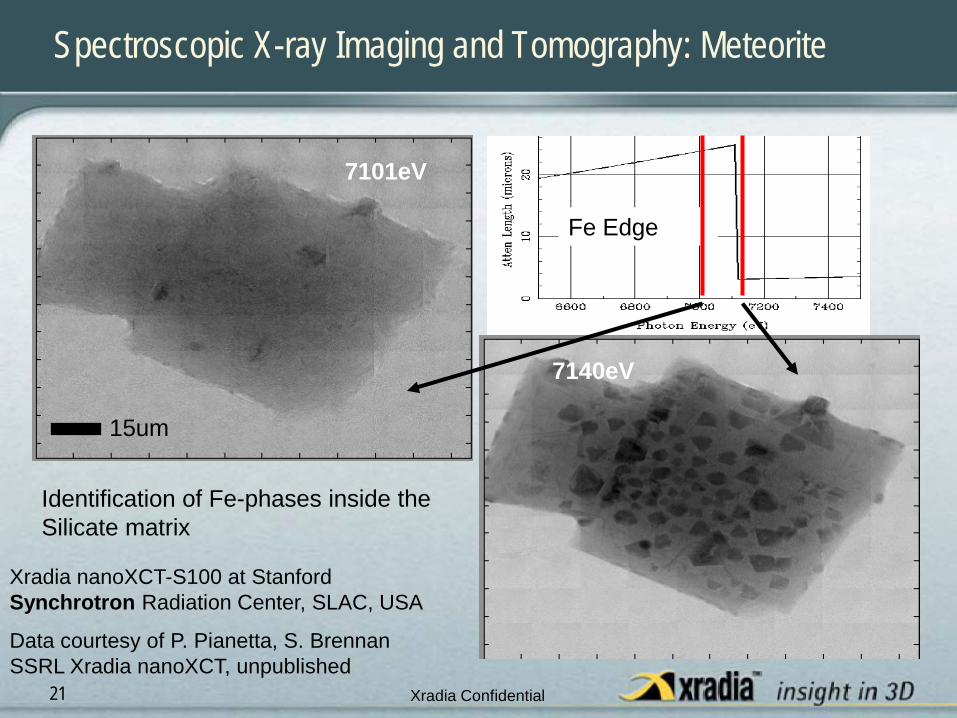
Spectroscopic X-ray Imaging and Tomography: Meteorite
15um
7101eV
7140eV
Fe Edge
Identification of Fe-phases inside the Silicate matrix
Xradia nanoXCT-S100 at Stanford Synchrotron Radiation Center, SLAC, USA
Data courtesy of P. Pianetta, S. BrennanSSRL Xradia nanoXCT, unpublished

22 Xradia Confidential
Some published TXM data from Synchrotron : Cu-low k
Sneider et al, Future Fab Vol 19, section 8
High Resolution
& High Contrast

23 Xradia Confidential
Application : Electromigration- insitu
Sneider et al, Future Fab Vol 19, section 8
Typical Synchrotron set up
Cu via line test segment

24 Xradia Confidential
Application : Electromigration- insitu
Sneider et al, Future Fab Vol 19, section 8
Passivated Cu interconnect. Thickness
350 nm, line width 600nm.
Via stressed at temp 230 deg C
Current densities increased up to 10e7
A/cm3 during 16 hrs, 52 min

25 Xradia Confidential
PCB
chipcrack
Delamination at edge
500um500um500um
500um500um
C4 Bump on Flip-chip Wire bond packaging GaAs III/V IC Package
Solder Balls and Via Crack Solder Balls and Via Joint CrackDelamination on Thin Die
Selected Imaging Applications for IC Packaging(MicroXCT)

26 Xradia Confidential
Etched Through Si Via on glass carrier imaged at 1 um resolution with MicroXCT
89.6um
49.3um
41.1um
53.7um
47.1um

27 Xradia Confidential
Non invasive void characterization: CT slices at 50 nm
Virtual slices from a 10 μm via. The via has a ~ 5 μm void in the center
(1)
(3)
(4)
(5)
10 μ
m
(2)
5 μm

28 Xradia Confidential
1. Solder non wet
Complete non wettaken from entire tomography
Cracked ball taken from 20s scan, limited angle

29 Xradia Confidential
Conclusions
X-ray nondestructive 3D imaging with 30nm resolution has been developed for Cu interconnect characterization
X-ray nondestructive 3D imaging offers good capability for TSV development and FA applications
Time lapse imaging using x-rays can be used to study reliability issues