WT51F116/108 1T 8052 Micro-controller with ADC Function ...€¦ · 1T 8052 Micro -controller with...
184
WT51F116/108 1T 8052 Micro-controller with ADC Function Copyright 2014 Weltrend Semiconductor, Inc. All Rights Reserved. Weltrend reserves right to modify all information contained in this document without notice. WT51F116/108 1T 8052 Micro-controller with ADC Function (FLASH) Data Sheet Rev. 1.0 December 2014 Copyright Notice This data sheet is copyrighted by Weltrend Semiconductor, Inc. Do not reproduce, transform to any other format, or send/transmit any part of this documentation without the express written permission of Weltrend Semiconductor, Inc. Disclaimers Right to make change – This document provides technical information for user. Weltrend Semiconductor, Inc. reserves the right to make change without further notice to any products herein.
Transcript of WT51F116/108 1T 8052 Micro-controller with ADC Function ...€¦ · 1T 8052 Micro -controller with...
WT51F116/108 1T 8052 Micro-controller with ADC Function
Copyright 2014 Weltrend Semiconductor, Inc. All Rights Reserved. Weltrend reserves right to modify all information contained in this document without notice.
WT51F116/108 1T 8052 Micro-controller
with ADC Function (FLASH)
Data Sheet
Rev. 1.0
December 2014
Copyright Notice This data sheet is copyrighted by Weltrend Semiconductor, Inc. Do not reproduce, transform to any other format, or send/transmit any part of this documentation without the express written permission of Weltrend Semiconductor, Inc. Disclaimers Right to make change – This document provides technical information for user. Weltrend Semiconductor, Inc. reserves the right to make change without further notice to any products herein.
WT51F116/108 1T 8052 Micro-controller with ADC Function
Copyright 2014 Weltrend Semiconductor, Inc. All Rights Reserved. Weltrend reserves right to modify all information contained in this document without notice.
- 1 -
Table of Contents
1. General Description ..................................................................................................................... 3
2. Features ........................................................................................................................................ 3
3. Block Diagram .............................................................................................................................. 4 3.1 System Clock Tree.................................................................................................................................. 5
4. Pin Configuration ......................................................................................................................... 6 4.1 Pin Description ........................................................................................................................................ 8 4.2 Pin Summary ........................................................................................................................................12 4.3 Port Structure ........................................................................................................................................14
5. Normal Function ......................................................................................................................... 19 5.1 CPU ......................................................................................................................................................19 5.2 RAM ......................................................................................................................................................19 5.3 Flash Memory .......................................................................................................................................21 5.4 Memory Mapping ..................................................................................................................................22 5.5 In-System Programming (ISP) (Important!!! Must Read!!!) ..................................................................26 5.6 Timer/Counter .......................................................................................................................................29 5.7 Reset ....................................................................................................................................................35 5.8 System Clock and Clock sources .........................................................................................................37
6. Enhanced Function .................................................................................................................... 39 6.1 External Special Function Register (XFR) ............................................................................................39 6.2 I/O Port .................................................................................................................................................44 6.3 Interrupt ................................................................................................................................................58 6.4 Universal Asynchronous Receiver-Transmitter (UART) .......................................................................70 6.5 External Interrupt Request (IRQ) ..........................................................................................................75 6.6 Pulse Width Modulation (PWM) ............................................................................................................80 6.7 Power Management .............................................................................................................................90 6.8 12 MHz/24 MHz RC Oscillator Calibration .........................................................................................104 6.9 Watchdog Timer and Watch Timer .....................................................................................................108 6.10 I²C Serial Interface .............................................................................................................................. 112 6.11 Enhanced Timer/Counter .................................................................................................................... 117 6.12 Serial Peripheral Interface (SPI) .........................................................................................................122 6.13 Analog/Digital Converter (ADC) ..........................................................................................................128 6.14 Comparator .........................................................................................................................................134 6.15 Low Voltage Detection (LVD) ..............................................................................................................138 6.16 Low Voltage Detection Reset (LVDR) .................................................................................................139 6.17 Emulated E²PROM .............................................................................................................................141 6.18 Code Option ........................................................................................................................................145 6.19 Read Out Protection & Encryption......................................................................................................155 6.20 Internal Voltage Reference Source (BandGap) ..................................................................................156
WT51F116/108 1T 8052 Micro-controller with ADC Function
Copyright 2014 Weltrend Semiconductor, Inc. All Rights Reserved. Weltrend reserves right to modify all information contained in this document without notice.
- 2 -
7. Electrical Characteristics ......................................................................................................... 157 7.1 Absolute Maximum Ratings ................................................................................................................157 7.2 Recommended Operating Parameters ...............................................................................................157 7.3 DC Electrical Characteristics (VDD = 1.8V ~ 5V, -40℃ ~ +105℃) .....................................................158 7.4 AC Electrical Characteristics (TA = 25℃) ...........................................................................................160 7.5 Internal RC Oscillator Temperature Tolerance table ...........................................................................161 7.6 A/D Converting Characteristics (TA = 25℃) .......................................................................................162 7.7 Bandgap Electrical Characteristic.......................................................................................................163 7.8 Low Voltage Reset (LVR), Low Voltage Detection (LVD) & Low Voltage Detection Reset (LVDR) Electrical Characteristics (TA = 25℃) ............................................................................................................164 7.9 Comparator Characteristics (VDD = 5V, TA = 25℃) .............................................................................164 7.10 Thermal Resistance Notice ................................................................................................................165
8. Application Circuits ................................................................................................................. 166 8.1 Power Supply ......................................................................................................................................166 8.2 Oscillator Circuits ................................................................................................................................167 8.3 RESET Circuit .....................................................................................................................................169 8.4 Standard Circuit ..................................................................................................................................170 8.5 Development board circuits (16*2 LCM).............................................................................................171
9. Product Naming Rule ............................................................................................................... 172
10. Ordering Information ............................................................................................................... 172
11. Pad Diagram & Location Table ................................................................................................ 173
12. Package Dimension ................................................................................................................. 175 12.1 32-Pin QFN .........................................................................................................................................175 12.2 20-Pin SSOP ......................................................................................................................................176 12.3 10-Pin MSOP ......................................................................................................................................177
13. Development Tools .................................................................................................................. 178
14. Revision History ....................................................................................................................... 182
Appendix: Errata ............................................................................................................................. 183
WT51F116/108 1T 8052 Micro-controller with ADC Function
Copyright 2014 Weltrend Semiconductor, Inc. All Rights Reserved. Weltrend reserves right to modify all information contained in this document without notice.
- 3 -
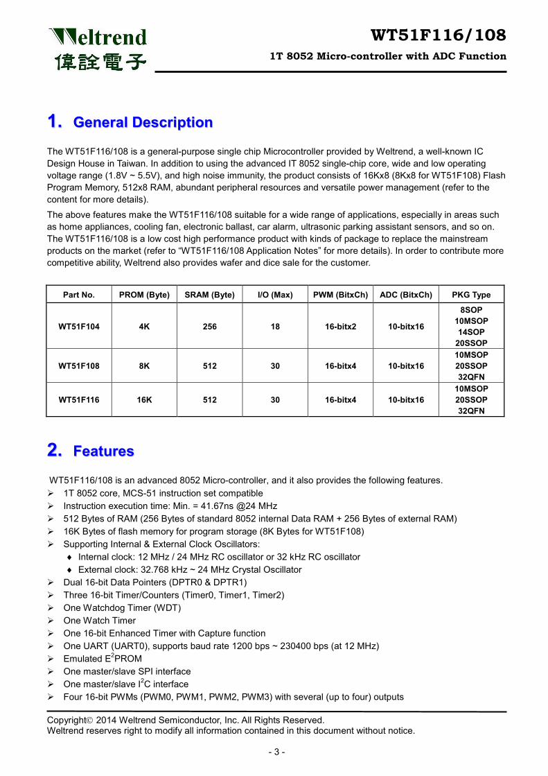
The WT51F116/108 is a general-purpose single chip Microcontroller provided by Weltrend, a well-known IC Design House in Taiwan. In addition to using the advanced IT 8052 single-chip core, wide and low operating voltage range (1.8V ~ 5.5V), and high noise immunity, the product consists of 16Kx8 (8Kx8 for WT51F108) Flash Program Memory, 512x8 RAM, abundant peripheral resources and versatile power management (refer to the content for more details). The above features make the WT51F116/108 suitable for a wide range of applications, especially in areas such as home appliances, cooling fan, electronic ballast, car alarm, ultrasonic parking assistant sensors, and so on. The WT51F116/108 is a low cost high performance product with kinds of package to replace the mainstream products on the market (refer to “WT51F116/108 Application Notes” for more details). In order to contribute more competitive ability, Weltrend also provides wafer and dice sale for the customer.
Part No. PROM (Byte) SRAM (Byte) I/O (Max) PWM (BitxCh) ADC (BitxCh) PKG Type
WT51F104 4K 256 18 16-bitx2 10-bitx16
8SOP 10MSOP 14SOP
20SSOP
WT51F108 8K 512 30 16-bitx4 10-bitx16 10MSOP 20SSOP 32QFN
WT51F116 16K 512 30 16-bitx4 10-bitx16 10MSOP 20SSOP 32QFN
WT51F116/108 is an advanced 8052 Micro-controller, and it also provides the following features. 1T 8052 core, MCS-51 instruction set compatible Instruction execution time: Min. = 41.67ns @24 MHz 512 Bytes of RAM (256 Bytes of standard 8052 internal Data RAM + 256 Bytes of external RAM) 16K Bytes of flash memory for program storage (8K Bytes for WT51F108) Supporting Internal & External Clock Oscillators:
♦ Internal clock: 12 MHz / 24 MHz RC oscillator or 32 kHz RC oscillator ♦ External clock: 32.768 kHz ~ 24 MHz Crystal Oscillator
Dual 16-bit Data Pointers (DPTR0 & DPTR1) Three 16-bit Timer/Counters (Timer0, Timer1, Timer2) One Watchdog Timer (WDT) One Watch Timer One 16-bit Enhanced Timer with Capture function One UART (UART0), supports baud rate 1200 bps ~ 230400 bps (at 12 MHz) Emulated E2PROM One master/slave SPI interface One master/slave I2C interface Four 16-bit PWMs (PWM0, PWM1, PWM2, PWM3) with several (up to four) outputs
11.. GGeenneerraall DDeessccrriippttiioonn
22.. FFeeaattuurreess
WT51F116/108 1T 8052 Micro-controller with ADC Function
Copyright 2014 Weltrend Semiconductor, Inc. All Rights Reserved. Weltrend reserves right to modify all information contained in this document without notice.
- 4 -
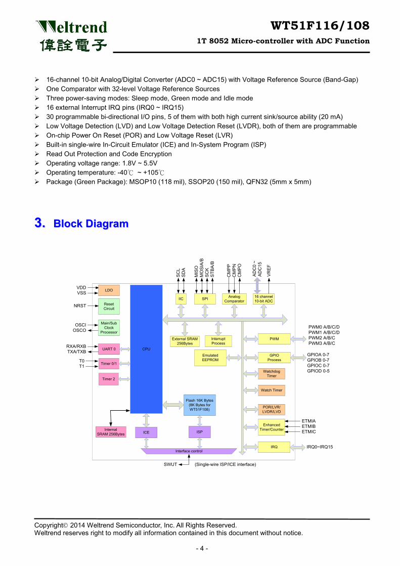
16-channel 10-bit Analog/Digital Converter (ADC0 ~ ADC15) with Voltage Reference Source (Band-Gap) One Comparator with 32-level Voltage Reference Sources Three power-saving modes: Sleep mode, Green mode and Idle mode 16 external Interrupt IRQ pins (IRQ0 ~ IRQ15) 30 programmable bi-directional I/O pins, 5 of them with both high current sink/source ability (20 mA) Low Voltage Detection (LVD) and Low Voltage Detection Reset (LVDR), both of them are programmable On-chip Power On Reset (POR) and Low Voltage Reset (LVR) Built-in single-wire In-Circuit Emulator (ICE) and In-System Program (ISP) Read Out Protection and Code Encryption Operating voltage range: 1.8V ~ 5.5V Operating temperature: -40℃ ~ +105℃ Package (Green Package): MSOP10 (118 mil), SSOP20 (150 mil), QFN32 (5mm x 5mm)
CPU
Reset Circuit
PWM
IIC SPI
GPIOProcess
WatchdogTimer
Watch Timer
AnalogComparator
16 channel10-bit ADC
EnhancedTimer/Counter
POR/LVR/LVDR/LVD
InternalSRAM 256Bytes
Flash 16K Bytes(8K Bytes for WT51F108)
InterruptProcess
ISP
Interface control
ICE
SC
LS
DA
MIS
OM
OS
IA/B
SC
KS
TBA
/B
Timer 0/1
AD
C0
~A
DC
15
CM
PP
CM
PN
CM
PO
GPIOA 0-7GPIOB 0-7GPIOC 0-7GPIOD 0-5
VDDVSS
NRST
OSCIOSCO
SWUT
VR
EF
Main/Sub Clock
Processor
UART 0
Emulated EEPROM
RXA/RXBTXA/TXB
LDO
ETMIAETMIB
(Single-wire ISP/ICE interface)
IRQ IRQ0~IRQ15
PWM0 A/B/C/DPWM1 A/B/C/DPWM2 A/B/CPWM3 A/B/C
External SRAM 256Bytes
Timer 2
T1T0
ETMIC
33.. BBlloocckk DDiiaaggrraamm
WT51F116/108 1T 8052 Micro-controller with ADC Function
Copyright 2014 Weltrend Semiconductor, Inc. All Rights Reserved. Weltrend reserves right to modify all information contained in this document without notice.
- 5 -
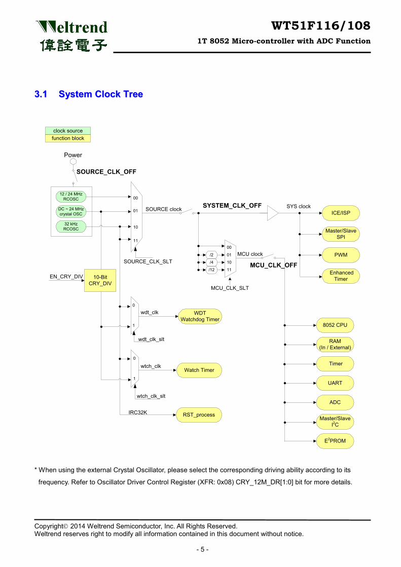
33..11 SSyysstteemm CClloocckk TTrreeee
DC ~ 24 MHzcrystal OSC
clock sourcefunction block
ICE/ISP
ADC
Master/Slave SPI
Master/SlaveI2C
PWM
Timer
UART
8052 CPU
RAM(In / External)
12 / 24 MHzRCOSC
Enhanced Timer
E2PROM
SOURCE_CLK_SLT
SOURCE clock
MCU clock
00
01
10
11
32 kHzRCOSC
MCU_CLK_SLT
00
01
10
11
/2
/4
/12
WDT Watchdog Timer
Watch Timer
0
1
wdt_clk_slt
0
1
wtch_clk_slt
wdt_clk
wtch_clk
RST_processIRC32K
SYS clock
Power
MCU_CLK_OFF
SYSTEM_CLK_OFF
SOURCE_CLK_OFF
10-BitCRY_DIV
EN_CRY_DIV
* When using the external Crystal Oscillator, please select the corresponding driving ability according to its
frequency. Refer to Oscillator Driver Control Register (XFR: 0x08) CRY_12M_DR[1:0] bit for more details.
WT51F116/108 1T 8052 Micro-controller with ADC Function
Copyright 2014 Weltrend Semiconductor, Inc. All Rights Reserved. Weltrend reserves right to modify all information contained in this document without notice.
- 6 -
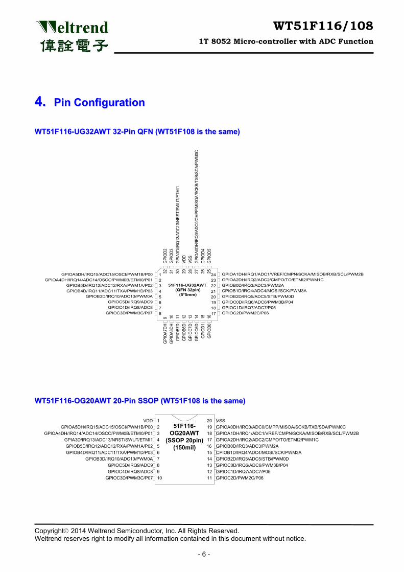
WWTT5511FF111166--UUGG3322AAWWTT 3322--PPiinn QQFFNN ((WWTT5511FF110088 iiss tthhee ssaammee))
2423222120191817 GPIOC2D/PWM2C/P06
GPIOA5DH/IRQ15/ADC15/OSCI/PWM1B/P00
GPI
OA7
DH9 10 11 12 13 14 15 16
2526272829303132
GPI
OD5
12345678
GPIOA4DH/IRQ14/ADC14/OSCO/PWM0B/ETMI0/P01GPIOB5D/IRQ12/ADC12/RXA/PWM1A/P02GPIOB4D/IRQ11/ADC11/TXA/PWM1D/P03
GPIOB3D/IRQ10/ADC10/PWM0AGPIOC5D/IRQ9/ADC9GPIOC4D/IRQ8/ADC8
GPIOC3D/PWM3C/P07
GPI
OA6
DHG
PIO
B7D
GPI
OB6
DG
PIO
C7D
GPI
OC6
DG
PIO
D1G
PIO
D0
GPIOC1D/IRQ7/ADC7/P05GPIOC0D/IRQ6/ADC6/PWM3B/P04GPIOB2D/IRQ5/ADC5/STB/PWM0DCPIOB1D/IRQ4/ADC4/MOSI/SCK/PWM3AGPIOB0D/IRQ3/ADC3/PWM2AGPIOA2DH/IRQ2/ADC2/CMPO/TO/ETMI2/PWM1CGPIOA1DH/IRQ1/ADC1/VREF/CMPN/SCKA/MISOB/RXB/SCL/PWM2B
GPI
OD4
GPI
OA0
DH/IR
Q0/
ADC0
/CM
PP/M
ISO
A/SC
KB/T
XB/S
DA/P
WM
0CVS
SVD
DG
PIA3
D/IR
Q13
/ADC
13/N
RST/
SWUT
/ETM
I1G
PIO
D3G
PIO
D2
51F116-UG32AWT (QFN 32pin)
(5*5mm)
WWTT5511FF111166--OOGG2200AAWWTT 2200--PPiinn SSSSOOPP ((WWTT5511FF110088 iiss tthhee ssaammee))
51F116-OG20AWT
(SSOP 20pin)(150mil)
1817
1234 GPIOA2DH/IRQ2/ADC2/CMPO/TO/ETMI2/PWM1C
GPIOA4DH/IRQ14/ADC14/OSCO/PWM0B/ETMI0/P01
VDDGPIOA5DH/IRQ15/ADC15/OSCI/PWM1B/P00
GPIA3D/IRQ13/ADC13/NRST/SWUT/ETMI1
VSS
567
GPIOB4D/IRQ11/ADC11/TXA/PWM1D/P03GPIOB5D/IRQ12/ADC12/RXA/PWM1A/P02
GPIOB3D/IRQ10/ADC10/PWM0A
161514 GPIOB2D/IRQ5/ADC5/STB/PWM0D
GPIOB0D/IRQ3/ADC3/PWM2ACPIOB1D/IRQ4/ADC4/MOSI/SCK/PWM3A
89
GPIOC5D/IRQ9/ADC9GPIOC4D/IRQ8/ADC8
11GPIOC1D/IRQ7/ADC7/P0512GPIOC0D/IRQ6/ADC6/PWM3B/P0413
GPIOA0DH/IRQ0/ADC0/CMPP/MISOA/SCKB/TXB/SDA/PWM0C
10GPIOC3D/PWM3C/P07 GPIOC2D/PWM2C/P06
1920
GPIOA1DH/IRQ1/ADC1/VREF/CMPN/SCKA/MISOB/RXB/SCL/PWM2B
44.. PPiinn CCoonnffiigguurraattiioonn
WT51F116/108 1T 8052 Micro-controller with ADC Function
Copyright 2014 Weltrend Semiconductor, Inc. All Rights Reserved. Weltrend reserves right to modify all information contained in this document without notice.
- 7 -
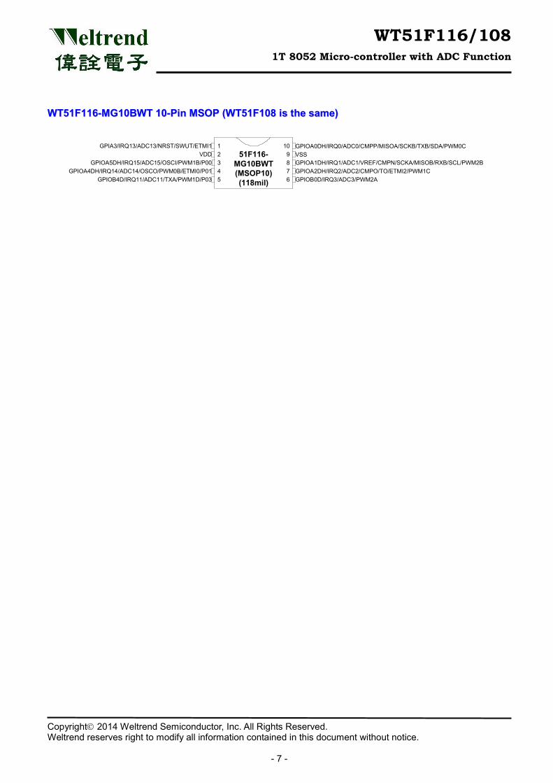
WWTT5511FF111166--MMGG1100BBWWTT 1100--PPiinn MMSSOOPP ((WWTT5511FF110088 iiss tthhee ssaammee))
51F116-MG10BWT(MSOP10)(118mil)
1234 GPIOA2DH/IRQ2/ADC2/CMPO/TO/ETMI2/PWM1C
GPIA3/IRQ13/ADC13/NRST/SWUT/ETMI1VDD VSS
5 67
GPIOB4D/IRQ11/ADC11/TXA/PWM1D/P03
10
GPIOB0D/IRQ3/ADC3/PWM2A
89
GPIOA1DH/IRQ1/ADC1/VREF/CMPN/SCKA/MISOB/RXB/SCL/PWM2B
GPIOA0DH/IRQ0/ADC0/CMPP/MISOA/SCKB/TXB/SDA/PWM0C
GPIOA5DH/IRQ15/ADC15/OSCI/PWM1B/P00GPIOA4DH/IRQ14/ADC14/OSCO/PWM0B/ETMI0/P01
WT51F116/108 1T 8052 Micro-controller with ADC Function
Copyright 2014 Weltrend Semiconductor, Inc. All Rights Reserved. Weltrend reserves right to modify all information contained in this document without notice.
- 8 -
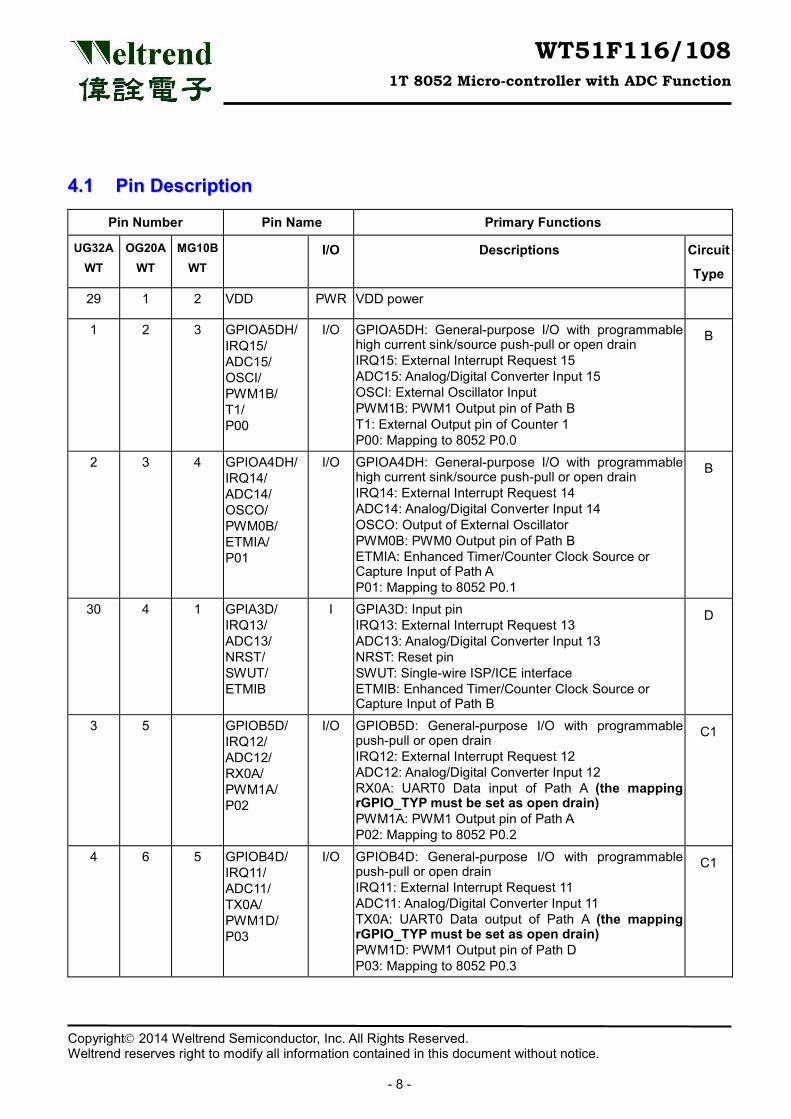
44..11 PPiinn DDeessccrriippttiioonn
Pin Number Pin Name Primary Functions
UG32A WT
OG20A WT
MG10B WT
I/O Descriptions Circuit
Type
29 1 2 VDD PWR VDD power
1 2 3 GPIOA5DH/ IRQ15/ ADC15/ OSCI/ PWM1B/ T1/ P00
I/O GPIOA5DH: General-purpose I/O with programmable high current sink/source push-pull or open drain IRQ15: External Interrupt Request 15 ADC15: Analog/Digital Converter Input 15 OSCI: External Oscillator Input PWM1B: PWM1 Output pin of Path B T1: External Output pin of Counter 1 P00: Mapping to 8052 P0.0
B
2 3 4 GPIOA4DH/ IRQ14/ ADC14/ OSCO/ PWM0B/ ETMIA/ P01
I/O GPIOA4DH: General-purpose I/O with programmable high current sink/source push-pull or open drain IRQ14: External Interrupt Request 14 ADC14: Analog/Digital Converter Input 14 OSCO: Output of External Oscillator PWM0B: PWM0 Output pin of Path B ETMIA: Enhanced Timer/Counter Clock Source or Capture Input of Path A P01: Mapping to 8052 P0.1
B
30 4 1 GPIA3D/ IRQ13/ ADC13/ NRST/ SWUT/ ETMIB
I GPIA3D: Input pin IRQ13: External Interrupt Request 13 ADC13: Analog/Digital Converter Input 13 NRST: Reset pin SWUT: Single-wire ISP/ICE interface ETMIB: Enhanced Timer/Counter Clock Source or Capture Input of Path B
D
3 5 GPIOB5D/ IRQ12/ ADC12/ RX0A/ PWM1A/ P02
I/O GPIOB5D: General-purpose I/O with programmable push-pull or open drain IRQ12: External Interrupt Request 12 ADC12: Analog/Digital Converter Input 12 RX0A: UART0 Data input of Path A (the mapping rGPIO_TYP must be set as open drain) PWM1A: PWM1 Output pin of Path A P02: Mapping to 8052 P0.2
C1
4 6 5 GPIOB4D/ IRQ11/ ADC11/ TX0A/ PWM1D/ P03
I/O GPIOB4D: General-purpose I/O with programmable push-pull or open drain IRQ11: External Interrupt Request 11 ADC11: Analog/Digital Converter Input 11 TX0A: UART0 Data output of Path A (the mapping rGPIO_TYP must be set as open drain) PWM1D: PWM1 Output pin of Path D P03: Mapping to 8052 P0.3
C1
WT51F116/108 1T 8052 Micro-controller with ADC Function
Copyright 2014 Weltrend Semiconductor, Inc. All Rights Reserved. Weltrend reserves right to modify all information contained in this document without notice.
- 9 -
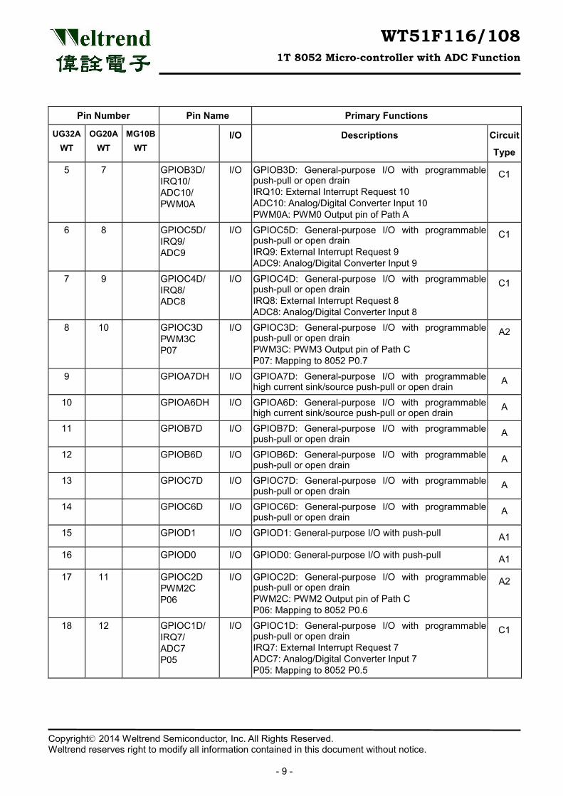
Pin Number Pin Name Primary Functions
UG32A WT
OG20A WT
MG10B WT
I/O Descriptions Circuit
Type
5 7 GPIOB3D/ IRQ10/ ADC10/ PWM0A
I/O GPIOB3D: General-purpose I/O with programmable push-pull or open drain IRQ10: External Interrupt Request 10 ADC10: Analog/Digital Converter Input 10 PWM0A: PWM0 Output pin of Path A
C1
6 8 GPIOC5D/ IRQ9/ ADC9
I/O GPIOC5D: General-purpose I/O with programmable push-pull or open drain IRQ9: External Interrupt Request 9 ADC9: Analog/Digital Converter Input 9
C1
7 9 GPIOC4D/ IRQ8/ ADC8
I/O GPIOC4D: General-purpose I/O with programmable push-pull or open drain IRQ8: External Interrupt Request 8 ADC8: Analog/Digital Converter Input 8
C1
8 10 GPIOC3D PWM3C P07
I/O GPIOC3D: General-purpose I/O with programmable push-pull or open drain PWM3C: PWM3 Output pin of Path C P07: Mapping to 8052 P0.7
A2
9 GPIOA7DH I/O GPIOA7D: General-purpose I/O with programmable high current sink/source push-pull or open drain A
10 GPIOA6DH I/O GPIOA6D: General-purpose I/O with programmable high current sink/source push-pull or open drain A
11 GPIOB7D I/O GPIOB7D: General-purpose I/O with programmable push-pull or open drain A
12 GPIOB6D I/O GPIOB6D: General-purpose I/O with programmable push-pull or open drain A
13 GPIOC7D I/O GPIOC7D: General-purpose I/O with programmable push-pull or open drain A
14 GPIOC6D I/O GPIOC6D: General-purpose I/O with programmable push-pull or open drain A
15 GPIOD1 I/O GPIOD1: General-purpose I/O with push-pull A1
16 GPIOD0 I/O GPIOD0: General-purpose I/O with push-pull A1
17 11 GPIOC2D PWM2C P06
I/O GPIOC2D: General-purpose I/O with programmable push-pull or open drain PWM2C: PWM2 Output pin of Path C P06: Mapping to 8052 P0.6
A2
18 12 GPIOC1D/ IRQ7/ ADC7 P05
I/O GPIOC1D: General-purpose I/O with programmable push-pull or open drain IRQ7: External Interrupt Request 7 ADC7: Analog/Digital Converter Input 7 P05: Mapping to 8052 P0.5
C1
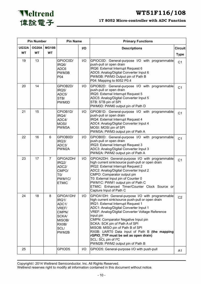
WT51F116/108 1T 8052 Micro-controller with ADC Function
Copyright 2014 Weltrend Semiconductor, Inc. All Rights Reserved. Weltrend reserves right to modify all information contained in this document without notice.
- 10 -
Pin Number Pin Name Primary Functions
UG32A WT
OG20A WT
MG10B WT
I/O Descriptions Circuit
Type
19 13 GPIOC0D/ IRQ6/ ADC6 PWM3B P04
I/O GPIOC0D: General-purpose I/O with programmable push-pull or open drain IRQ6: External Interrupt Request 6 ADC6: Analog/Digital Converter Input 6 PWM3B: PWM3 Output pin of Path B P04: Mapping to 8052 P0.4
C1
20 14 GPIOB2D/ IRQ5/ ADC5/ STB/ PWM0D
I/O GPIOB2D: General-purpose I/O with programmable push-pull or open drain IRQ5: External Interrupt Request 5 ADC5: Analog/Digital Converter Input 5 STB: STB pin of SPI PWM0D: PWM0 output pin of Path D
C1
21 15 CPIOB1D/ IRQ4/ ADC4/ MOSI/ PWM3A
I/O GPIOB1D: General-purpose I/O with programmable push-pull or open drain IRQ4: External Interrupt Request 4 ADC4: Analog/Digital Converter Input 4 MOSI: MOSI pin of SPI PWM3A: PWM3 output pin of Path A
C1
22 16 6 GPIOB0D/ IRQ3/ ADC3/ PWM2A
I/O GPIOB0D: General-purpose I/O with programmable push-pull or open drain IRQ3: External Interrupt Request 3 ADC3: Analog/Digital Converter Input 3 PWM2A: PWM2 output pin of Path A
C1
23 17 7 GPIOA2DH/ IRQ2/ ADC2/ CMPO/ T0/ PWM1C/ ETMIC
I/O GPIOA2DH: General-purpose I/O with programmable high current sink/source push-pull or open drain IRQ2: External Interrupt Request 2 ADC2: Analog/Digital Converter Input 2 CMPO: Comparator output pin T0: External Input pin of Counter 0 PWM1C: PWM1 output pin of Path C ETMIC: Enhanced Timer/Counter Clock Source or Capture Input of Path C
C1
24 18 8 GPIOA1DH/ IRQ1/ ADC1/ VREF/ CMPN/ SCKA/ MISOB/ RX0B/ SCL/ PWM2B
I/O GPIOA1DH: General-purpose I/O with programmable high current sink/source push-pull or open drain IRQ1: External Interrupt Request 1 ADC1: Analog/Digital Converter Input 1 VREF: Analog/Digital Converter Voltage Reference input pin CMPN: Comparator Negative Input pin SCKA: SCK pin of Path A of SPI MISOB: MISO pin of Path B of SPI RX0B: UART0 Data input of Path B (the mapping rGPIO_TYP must be set as open drain) SCL: SCL pin of I²C PWM2B: PWM2 output pin of Path B
C2
25 GPIOD5 I/O GPIOD5: General-purpose I/O with push-pull A1
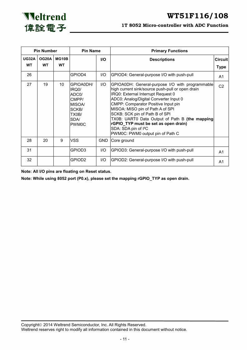
WT51F116/108 1T 8052 Micro-controller with ADC Function
Copyright 2014 Weltrend Semiconductor, Inc. All Rights Reserved. Weltrend reserves right to modify all information contained in this document without notice.
- 11 -
Pin Number Pin Name Primary Functions
UG32A WT
OG20A WT
MG10B WT
I/O Descriptions Circuit
Type
26 GPIOD4 I/O GPIOD4: General-purpose I/O with push-pull A1
27 19 10 GPIOA0DH/ IRQ0/ ADC0/ CMPP/ MISOA/ SCKB/ TX0B/ SDA/ PWM0C
I/O GPIOA0DH: General-purpose I/O with programmable high current sink/source push-pull or open drain IRQ0: External Interrupt Request 0 ADC0: Analog/Digital Converter Input 0 CMPP: Comparator Positive Input pin MISOA: MISO pin of Path A of SPI SCKB: SCK pin of Path B of SPI TX0B: UART0 Data Output of Path B (the mapping rGPIO_TYP must be set as open drain) SDA: SDA pin of I²C PWM0C: PWM0 output pin of Path C
C2
28 20 9 VSS GND Core ground
31 GPIOD3 I/O GPIOD3: General-purpose I/O with push-pull A1
32 GPIOD2 I/O GPIOD2: General-purpose I/O with push-pull A1
Note: All I/O pins are floating on Reset status. Note: While using 8052 port (P0.x), please set the mapping rGPIO_TYP as open drain.
WT51F116/108 1T 8052 Micro-controller with ADC Function
Copyright 2014 Weltrend Semiconductor, Inc. All Rights Reserved. Weltrend reserves right to modify all information contained in this document without notice.
- 12 -
44..22 PPiinn SSuummmmaarryy Explain each pin function in details.
Pin Name Type Description
PORT
GPIOA0 ~ GPIOA7 I/O 8-bit bidirectional general-purpose I/O port (GPIA3 is input only pin)
GPIOB0 ~ GPIOB7 I/O 8-bit bidirectional general-purpose I/O port
GPIOC0 ~ GPIOC7 I/O 8-bit bidirectional general-purpose I/O port
GPIOD0 ~ GPIOD5 I/O 6-bit bidirectional general-purpose I/O port
Timer 0/1
T0 I Timer/Counter 0 External Input
T1 I Timer/Counter 1 External Input
Enhanced Timer/Counter
ETMIA I Enhanced Timer/Counter Clock Source or Capture Input (Path A)
ETMIB I Enhanced Timer/Counter Clock Source or Capture Input (Path B)
ETMIC I Enhanced Timer/Counter Clock Source or Capture Input (Path C)
IRQ
IRQ0 ~ IRQ15 I 16 External Interrupt Request Input pins
PWM
PWM0 A/B/C/D O PWM 0 Output of Path A / Path B / Path C / Path D
PWM1 A/B/C/D O PWM 1 Output of Path A / Path B / Path C / Path D
PWM2 A/B/C O PWM 2 Output of Path A / Path B / Path C
PWM3 A/B/C O PWM 3 Output of Path A / Path B / Path C
UART
RX0 A/B I UART0 Receive Path A or Path B (the mapping rGPIO_TYP must be set as open drain)
TX0 A/B O UART0 Transmit Path A or Path B (the mapping rGPIO_TYP must be set as open drain)
SPI
SCKA I/O SPI Interface Clock of Path A
MISOA I/O SPI Data pin MISO (Master Input; Slave Output) of Path A
SCKB I/O SPI Interface Clock of Path B
MISOB I/O SPI Data pin MISO (Master Input; Slave Output) of Path B
MOSI I/O SPI Data pin MOSI (Master Output; Slave Input)
STB I/O SPI Enable
WT51F116/108 1T 8052 Micro-controller with ADC Function
Copyright 2014 Weltrend Semiconductor, Inc. All Rights Reserved. Weltrend reserves right to modify all information contained in this document without notice.
- 13 -
ADC
ADC0 ~ ADC15 I 16 Analog/Digital Input pins
ACOMP
CMPP I Comparator Positive Input pin
CMPN I Comparator Negative Input pin
CMPO O Comparator Output pin
I²C
SCL I/O I²C interface clock
SDA I/O I²C interface data
VCC & VSS
VDD P Power
VSS P Ground
OSCO O Main (Sub) oscillator output
OSCI I Main (Sub) oscillator input
NRST I CPU reset
ISP & ICE
SWUT I/O Single-wire ISP & ICE interface
WT51F116/108 1T 8052 Micro-controller with ADC Function
Copyright 2014 Weltrend Semiconductor, Inc. All Rights Reserved. Weltrend reserves right to modify all information contained in this document without notice.
- 14 -
44..33 PPoorrtt SSttrruuccttuurree
I/O Structure (Type A)
IO Pin
VSS
VSS
VDD
VDD
Weak pull up
GPIOx_D (data)
GPIOx_TYPE(open-drain_n)
GPIOx_PHN
0
1
CP
U d
ata
bus
GPIOx_OE (output enable)
Read GPIOx_D
VDD
IO structure (A type)
I/O Structure (Type A1)
IO Pin
VSS
VSS
VDD
VDD
Weak pull up
GPIOx_D (data)
GPIOx_PHN
0
1
CP
U d
ata
bus
GPIOx_OE (output enable)
Read GPIOx_D
VDD
A1 type IO structure
WT51F116/108 1T 8052 Micro-controller with ADC Function
Copyright 2014 Weltrend Semiconductor, Inc. All Rights Reserved. Weltrend reserves right to modify all information contained in this document without notice.
- 15 -
I/O Structure (Type A2)
IO Pin
VSS
VSS
VDD
VDD
Weak pull up
GPIOx_D (data)
GPIOx_TYPE(open-drain_n)
GPIOx_PHN
0
1
Function data
0
1
CP
U d
ata
bus
GPxx_FUN_SLT
GPIOx_OE (output enable)
Function output enable
Internal function input
Read GPIOx_D analog_FUN_SLT
VDD
A2 type IO structure
WT51F116/108 1T 8052 Micro-controller with ADC Function
Copyright 2014 Weltrend Semiconductor, Inc. All Rights Reserved. Weltrend reserves right to modify all information contained in this document without notice.
- 16 -
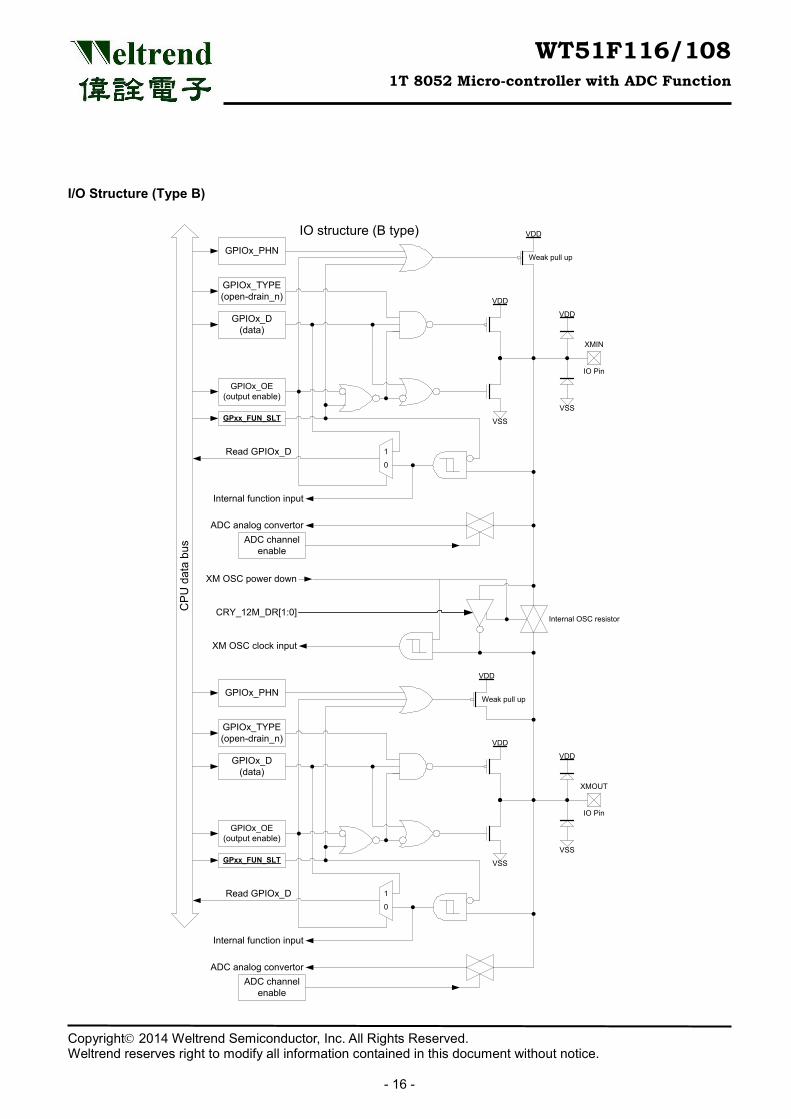
I/O Structure (Type B)
IO Pin
VSS
VSS
VDD
VDD
Weak pull up
GPIOx_D (data)
GPIOx_TYPE(open-drain_n)
GPIOx_PHN
0
1
CP
U d
ata
bus
GPxx_FUN_SLT
GPIOx_OE (output enable)
Read GPIOx_D
VDD
Internal OSC resistor
XM OSC clock input
IO Pin
VSS
VSS
VDD
VDD
Weak pull up
GPIOx_D (data)
GPIOx_TYPE(open-drain_n)
GPIOx_PHN
0
1
GPIOx_OE (output enable)
Read GPIOx_D
VDD
XMIN
XMOUT
XM OSC power down
CRY_12M_DR[1:0]
IO structure (B type)
Internal function input
ADC channel enable
ADC analog convertor
GPxx_FUN_SLT
Internal function input
ADC channel enable
ADC analog convertor
WT51F116/108 1T 8052 Micro-controller with ADC Function
Copyright 2014 Weltrend Semiconductor, Inc. All Rights Reserved. Weltrend reserves right to modify all information contained in this document without notice.
- 17 -
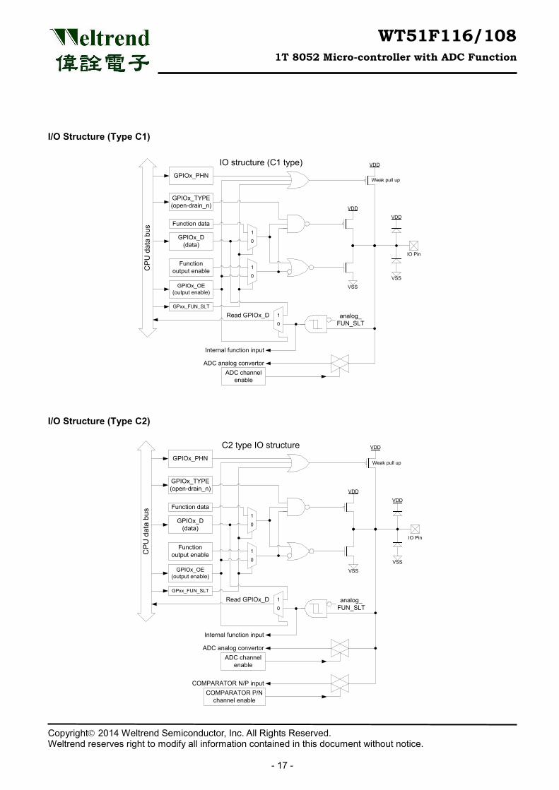
I/O Structure (Type C1)
IO Pin
VSS
VSS
VDD
VDD
Weak pull up
GPIOx_D (data)
GPIOx_TYPE(open-drain_n)
GPIOx_PHN
0
1
ADC channel enable
Function data
0
1
CP
U d
ata
bus
GPxx_FUN_SLT
GPIOx_OE (output enable)
Function output enable
0
1
Internal function input
ADC analog convertor
Read GPIOx_D analog_FUN_SLT
VDD
IO structure (C1 type)
I/O Structure (Type C2)
IO Pin
VSS
VSS
VDD
VDD
Weak pull up
GPIOx_D (data)
GPIOx_TYPE(open-drain_n)
GPIOx_PHN
0
1
ADC channel enable
Function data
0
1
CP
U d
ata
bus
GPxx_FUN_SLT
GPIOx_OE (output enable)
Function output enable
0
1
Internal function input
ADC analog convertor
Read GPIOx_D analog_FUN_SLT
VDD
C2 type IO structure
COMPARATOR P/N channel enable
COMPARATOR N/P input
WT51F116/108 1T 8052 Micro-controller with ADC Function
Copyright 2014 Weltrend Semiconductor, Inc. All Rights Reserved. Weltrend reserves right to modify all information contained in this document without notice.
- 18 -
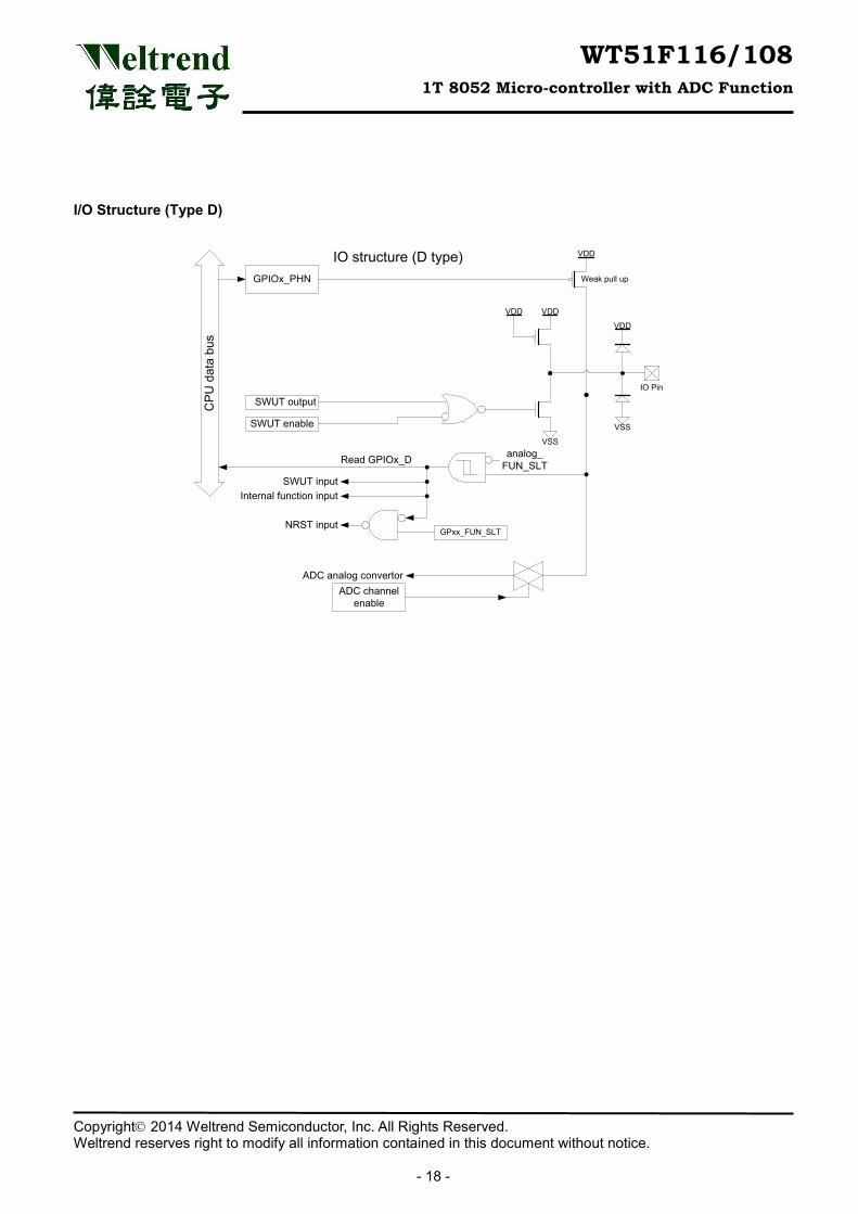
I/O Structure (Type D)
IO Pin
VSS
VSS
VDD
VDD
Weak pull upGPIOx_PHN
SWUT outputCP
U d
ata
bus
GPxx_FUN_SLT
SWUT enable
SWUT input
Read GPIOx_D
VDD
VDD
NRST input
IO structure (D type)
Internal function input
analog_FUN_SLT
ADC channel enable
ADC analog convertor
WT51F116/108 1T 8052 Micro-controller with ADC Function
Copyright 2014 Weltrend Semiconductor, Inc. All Rights Reserved. Weltrend reserves right to modify all information contained in this document without notice.
- 19 -
55..11 CCPPUU The WT51F116/108 has an embedded 8-bit 1T 8052 compatible CPU with 16-bit space addressable and 8-bit data access functions. The instruction execution time of 1T 8052 is three times faster than that of the conventional 3T 8052, and 12 times faster than that of 12T 8052. All of the functions and Special Function Register (SFR) definitions will be described in below sections.
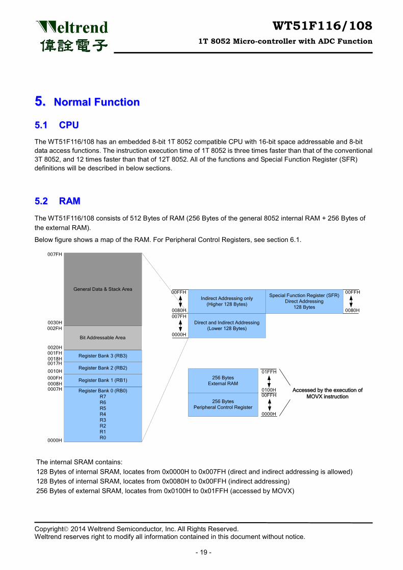
55..22 RRAAMM The WT51F116/108 consists of 512 Bytes of RAM (256 Bytes of the general 8052 internal RAM + 256 Bytes of the external RAM).
Below figure shows a map of the RAM. For Peripheral Control Registers, see section 6.1.
Indirect Addressing only(Higher 128 Bytes)
Direct and Indirect Addressing(Lower 128 Bytes)
00FFH
0080H007FH
0000H
Special Function Register (SFR)Direct Addressing
128 Bytes
00FFH
0080H
Register Bank 0 (RB0)R7R6R5R4R3R2R1R0
0007H
0000H
Register Bank 1 (RB1)000FH0008H
Register Bank 2 (RB2)0017H
0010H
Register Bank 3 (RB3)001FH0018H
Bit Addressable Area
002FH
0020H
General Data & Stack Area
007FH
0030H
256 BytesPeripheral Control Register
0000H
00FFHAccessed by the execution of
MOVX instruction
256 BytesExternal RAM
01FFH
0100H
The internal SRAM contains: 128 Bytes of internal SRAM, locates from 0x0000H to 0x007FH (direct and indirect addressing is allowed) 128 Bytes of internal SRAM, locates from 0x0080H to 0x00FFH (indirect addressing) 256 Bytes of external SRAM, locates from 0x0100H to 0x01FFH (accessed by MOVX)
55.. NNoorrmmaall FFuunnccttiioonn
WT51F116/108 1T 8052 Micro-controller with ADC Function
Copyright 2014 Weltrend Semiconductor, Inc. All Rights Reserved. Weltrend reserves right to modify all information contained in this document without notice.
- 20 -
Its main purpose is for storing data in the program, and therefore it is also called Data Memory. The Data memory of WT51F116/108 includes the following sections: (1) The lower 128 bytes of internal SRAM (0000H ~ 007FH) which can be accessed by direct or indirect
addressing are divided into 3 segments: General Purpose Register: Locates from 0000H to 001FH, 32 Bytes in total, can be divided into 4
register banks. Each register bank contains 8 general purpose registers (R0~R7). 4 register banks can be selected by the select bit RS1 and RS0 in the Program Status Word Register.
Bit Addressable Area: Locates from 20H to 2FH, 16 Bytes in total. Each one of the 128 bits of this segment can be directly addressed by Bit Addressing.
General Data Area: Locates from 0030H to 007FH, 80 Bytes are available to the user as data RAM (including the Stack area).
(2) The higher 128 bytes of internal SRAM (0080H ~ 00FFH) can be accessed by indirect addressing through R0 or R1 (*).
(3) Special Function Registers (SFR), locates from 0080H to 00FFH, can be accessed by direct addressing (*). (4) 256 Bytes of external SRAM, locates from 0x0100H to 0x01FFH, can be accessed by MOVX (indirect
addressing). (*) Although the SFR and the higher 128 Bytes of internal SRAM occupy the same addresses (0080H ~ 00FFH),
they are two separate areas. MCU will automatically determine which area is in use by two different accessing ways.
WT51F116/108 1T 8052 Micro-controller with ADC Function
Copyright 2014 Weltrend Semiconductor, Inc. All Rights Reserved. Weltrend reserves right to modify all information contained in this document without notice.
- 21 -
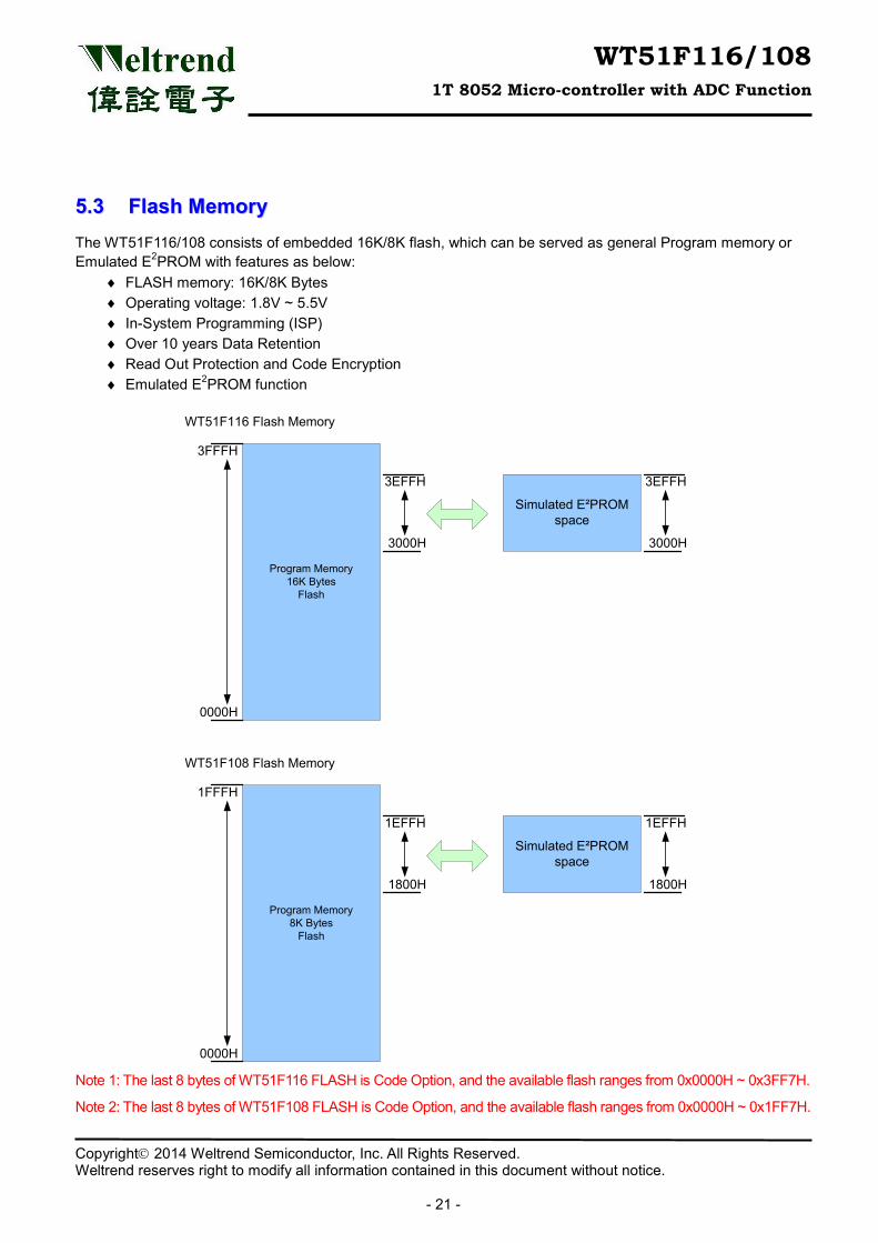
55..33 FFllaasshh MMeemmoorryy The WT51F116/108 consists of embedded 16K/8K flash, which can be served as general Program memory or Emulated E2PROM with features as below:
♦ FLASH memory: 16K/8K Bytes ♦ Operating voltage: 1.8V ~ 5.5V ♦ In-System Programming (ISP) ♦ Over 10 years Data Retention ♦ Read Out Protection and Code Encryption ♦ Emulated E2PROM function
Program Memory16K Bytes
Flash
3FFFH
0000H
Simulated E²PROMspace
3EFFH
3000H
3EFFH
3000H
WT51F116 Flash Memory
Program Memory8K Bytes
Flash
1FFFH
0000H
Simulated E²PROMspace
1EFFH
1800H
1EFFH
1800H
WT51F108 Flash Memory
Note 1: The last 8 bytes of WT51F116 FLASH is Code Option, and the available flash ranges from 0x0000H ~ 0x3FF7H.
Note 2: The last 8 bytes of WT51F108 FLASH is Code Option, and the available flash ranges from 0x0000H ~ 0x1FF7H.
WT51F116/108 1T 8052 Micro-controller with ADC Function
Copyright 2014 Weltrend Semiconductor, Inc. All Rights Reserved. Weltrend reserves right to modify all information contained in this document without notice.
- 22 -
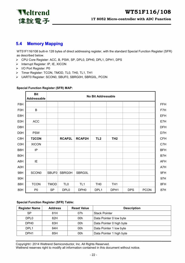
55..44 MMeemmoorryy MMaappppiinngg WT51F116/108 built-in 128 bytes of direct addressing register, with the standard Special Function Register (SFR) as described below. CPU Core Register: ACC, B, PSW, SP, DPL0, DPH0, DPL1, DPH1, DPS Interrupt Register: IP, IE, XICON I/O Port Register: P0 Timer Register: TCON, TMOD, TL0, TH0, TL1, TH1 UART0 Register: SCON0, SBUF0, SBRG0H, SBRG0L, PCON
Special Function Register (SFR) MAP:
Bit
Addressable No Bit Addressable
F8H FFH
F0H B F7H
E8H EFH
E0H ACC E7H
D8H DFH
D0H PSW D7H
C8H T2CON RCAP2L RCAP2H TL2 TH2 CFH
C0H XICON C7H
B8H IP BFH
B0H B7H
A8H IE AFH
A0H A7H
98H SCON0 SBUF0 SBRG0H SBRG0L 9FH
90H 97H
88H TCON TMOD TL0 TL1 TH0 TH1 8FH
80H P0 SP DPL0 DPH0 DPL1 DPH1 DPS PCON 87H
Special Function Register (SFR) Table:
Register Name Address Reset Value Description SP 81H 07h Stack Pointer
DPL0 82H 00h Data Pointer 0 low byte DPH0 83H 00h Data Pointer 0 high byte DPL1 84H 00h Data Pointer 1 low byte DPH1 85H 00h Data Pointer 1 high byte
WT51F116/108 1T 8052 Micro-controller with ADC Function
Copyright 2014 Weltrend Semiconductor, Inc. All Rights Reserved. Weltrend reserves right to modify all information contained in this document without notice.
- 23 -
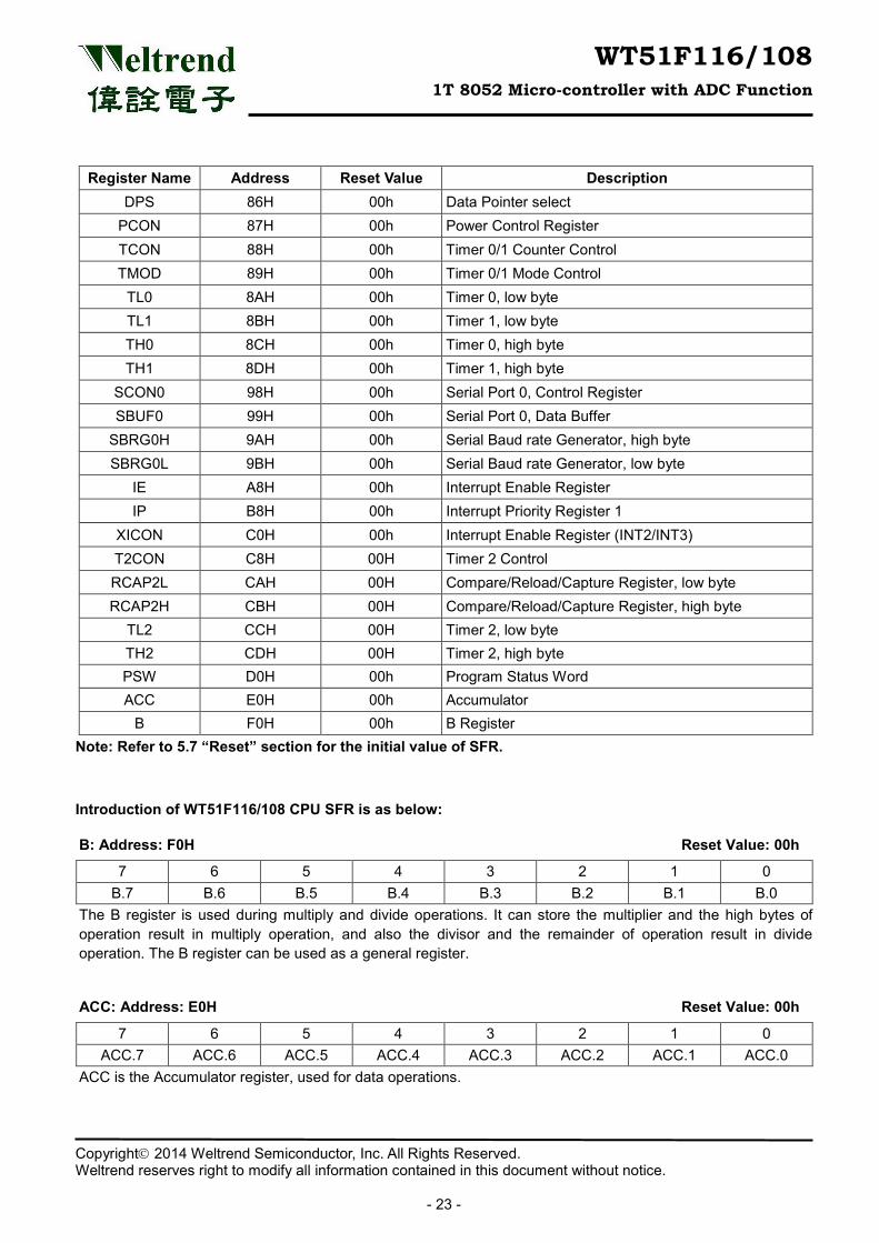
Register Name Address Reset Value Description DPS 86H 00h Data Pointer select
PCON 87H 00h Power Control Register TCON 88H 00h Timer 0/1 Counter Control TMOD 89H 00h Timer 0/1 Mode Control
TL0 8AH 00h Timer 0, low byte TL1 8BH 00h Timer 1, low byte TH0 8CH 00h Timer 0, high byte TH1 8DH 00h Timer 1, high byte
SCON0 98H 00h Serial Port 0, Control Register SBUF0 99H 00h Serial Port 0, Data Buffer
SBRG0H 9AH 00h Serial Baud rate Generator, high byte SBRG0L 9BH 00h Serial Baud rate Generator, low byte
IE A8H 00h Interrupt Enable Register IP B8H 00h Interrupt Priority Register 1
XICON C0H 00h Interrupt Enable Register (INT2/INT3) T2CON C8H 00H Timer 2 Control RCAP2L CAH 00H Compare/Reload/Capture Register, low byte RCAP2H CBH 00H Compare/Reload/Capture Register, high byte
TL2 CCH 00H Timer 2, low byte TH2 CDH 00H Timer 2, high byte PSW D0H 00h Program Status Word ACC E0H 00h Accumulator
B F0H 00h B Register Note: Refer to 5.7 “Reset” section for the initial value of SFR.
Introduction of WT51F116/108 CPU SFR is as below:
B: Address: F0H Reset Value: 00h
7 6 5 4 3 2 1 0 B.7 B.6 B.5 B.4 B.3 B.2 B.1 B.0
The B register is used during multiply and divide operations. It can store the multiplier and the high bytes of operation result in multiply operation, and also the divisor and the remainder of operation result in divide operation. The B register can be used as a general register.
ACC: Address: E0H Reset Value: 00h
7 6 5 4 3 2 1 0 ACC.7 ACC.6 ACC.5 ACC.4 ACC.3 ACC.2 ACC.1 ACC.0
ACC is the Accumulator register, used for data operations.
WT51F116/108 1T 8052 Micro-controller with ADC Function
Copyright 2014 Weltrend Semiconductor, Inc. All Rights Reserved. Weltrend reserves right to modify all information contained in this document without notice.
- 24 -
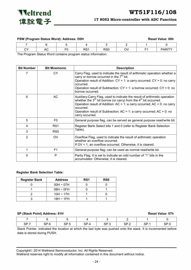
PSW (Program Status Word): Address: D0H Reset Value: 00h
7 6 5 4 3 2 1 0 CY AC F0 RS1 RS0 OV F1 PARITY
The Program Status Word contains program status information.
Bit Number Bit Mnemonic Description 7 CY Carry Flag, used to indicate the result of arithmetic operation whether a
carry or borrow occurred in the 7th bit. Operation result of Addition: CY = 1: a carry occurred; CY = 0: no carry occurred. Operation result of Subtraction: CY = 1: a borrow occurred; CY = 0: no borrow occurred.
6 AC Auxiliary-Carry Flag, used to indicate the result of arithmetic operation whether the 3rd bit borrow (or carry) from the 4th bit occurred. Operation result of Addition: AC = 1: a carry occurred; AC = 0: no carry occurred. Operation result of Subtraction: AC = 1: a carry occurred; AC = 0: no carry occurred.
5 F0 General purpose flag, can be served as general purpose read/write bit.
4 RS1 Register Bank Select bits 1 and 0 (refer to Register Bank Selection Table). 3 RS0
2 OV Overflow Flag, used to indicate the result of arithmetic operation whether an overflow occurred. If OV = 1, an overflow occurred. Otherwise, it is cleared.
1 F1 General-purpose flag, can be used as normal read/write bit.
0 P Parity Flag. It is set to indicate an odd number of “1” bits in the accumulator. Otherwise, it is cleared.
Register Bank Selection Table:
Register Bank Address RS1 RS0 0 00H ~ 07H 0 0 1 08H ~ 0FH 0 1 2 10H ~ 17H 1 0 3 18H ~ 1FH 1 1
SP (Stack Point) Address: 81H Reset Value: 07h
7 6 5 4 3 2 1 0 SP.7 SP.6 SP.5 SP.4 SP.3 SP.2 SP.1 SP.0
Stack Pointer, indicated the location at which the last byte was pushed onto the stack. It is incremented before data is stored during PUSH.
WT51F116/108 1T 8052 Micro-controller with ADC Function
Copyright 2014 Weltrend Semiconductor, Inc. All Rights Reserved. Weltrend reserves right to modify all information contained in this document without notice.
- 25 -
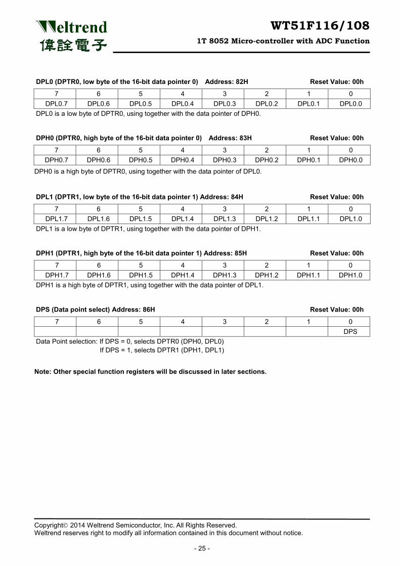
DPL0 (DPTR0, low byte of the 16-bit data pointer 0) Address: 82H Reset Value: 00h
7 6 5 4 3 2 1 0 DPL0.7 DPL0.6 DPL0.5 DPL0.4 DPL0.3 DPL0.2 DPL0.1 DPL0.0
DPL0 is a low byte of DPTR0, using together with the data pointer of DPH0.
DPH0 (DPTR0, high byte of the 16-bit data pointer 0) Address: 83H Reset Value: 00h
7 6 5 4 3 2 1 0 DPH0.7 DPH0.6 DPH0.5 DPH0.4 DPH0.3 DPH0.2 DPH0.1 DPH0.0
DPH0 is a high byte of DPTR0, using together with the data pointer of DPL0.
DPL1 (DPTR1, low byte of the 16-bit data pointer 1) Address: 84H Reset Value: 00h
7 6 5 4 3 2 1 0 DPL1.7 DPL1.6 DPL1.5 DPL1.4 DPL1.3 DPL1.2 DPL1.1 DPL1.0
DPL1 is a low byte of DPTR1, using together with the data pointer of DPH1.
DPH1 (DPTR1, high byte of the 16-bit data pointer 1) Address: 85H Reset Value: 00h
7 6 5 4 3 2 1 0 DPH1.7 DPH1.6 DPH1.5 DPH1.4 DPH1.3 DPH1.2 DPH1.1 DPH1.0
DPH1 is a high byte of DPTR1, using together with the data pointer of DPL1.
DPS (Data point select) Address: 86H Reset Value: 00h
7 6 5 4 3 2 1 0 DPS
Data Point selection: If DPS = 0, selects DPTR0 (DPH0, DPL0) If DPS = 1, selects DPTR1 (DPH1, DPL1) Note: Other special function registers will be discussed in later sections.
WT51F116/108 1T 8052 Micro-controller with ADC Function
Copyright 2014 Weltrend Semiconductor, Inc. All Rights Reserved. Weltrend reserves right to modify all information contained in this document without notice.
- 26 -
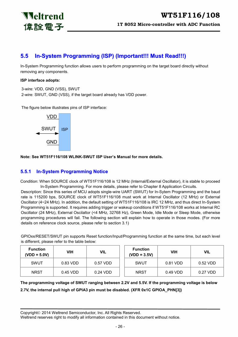
55..55 IInn--SSyysstteemm PPrrooggrraammmmiinngg ((IISSPP)) ((IImmppoorrttaanntt!!!!!! MMuusstt RReeaadd!!!!!!)) In-System Programming function allows users to perform programming on the target board directly without removing any components.
ISP interface adopts:
3-wire: VDD, GND (VSS), SWUT 2-wire: SWUT, GND (VSS), if the target board already has VDD power. The figure below illustrates pins of ISP interface:
ISP
VDD
SWUT
GND
Note: See WT51F116/108 WLINK-SWUT ISP User’s Manual for more details.
55..55..11 IInn--SSyysstteemm PPrrooggrraammmmiinngg NNoottiiccee
Condition: When SOURCE clock of WT51F116/108 is 12 MHz (Internal/External Oscillator), it is stable to proceed In-System Programming. For more details, please refer to Chapter 8 Application Circuits.
Description: Since this series of MCU adopts single-wire UART (SWUT) for In-Sytem Programming and the baud rate is 115200 bps, SOURCE clock of WT51F116/108 must work at Internal Oscillator (12 MHz) or External Oscillator (4~24 MHz). In addition, the default setting of WT51F116/108 is IRC 12 MHz, and thus direct In-System Programming is supported. It requires adding trigger or wakeup conditions if WT51F116/108 works at Internal RC Oscillator (24 MHz), External Oscilaltor (<4 MHz, 32768 Hz), Green Mode, Idle Mode or Sleep Mode, otherwise programming procedures will fail. The following section will explain how to operate in those modes. (For more details on reference clock source, please refer to section 3.1) GPIOxx/RESET/SWUT pin supports Reset function/Input/Programming function at the same time, but each level is different, please refer to the table below:
Function (VDD = 5.0V)
VIH VIL
SWUT 0.83 VDD 0.57 VDD
NRST 0.45 VDD 0.24 VDD
Function (VDD = 3.5V)
VIH VIL
SWUT 0.81 VDD 0.52 VDD
NRST 0.49 VDD 0.27 VDD
The programming voltage of SWUT ranging between 2.2V and 5.5V. If the programming voltage is below
2.7V, the internal pull high of GPIA3 pin must be disabled. (XFR 0x1C GPIOA_PHN[3])
WT51F116/108 1T 8052 Micro-controller with ADC Function
Copyright 2014 Weltrend Semiconductor, Inc. All Rights Reserved. Weltrend reserves right to modify all information contained in this document without notice.
- 27 -
NNoorrmmaall MMooddee::
If the SOURCE clock of WT51F116/108 works at Internal Oscillator (12 MHz) or External Oscillator (4~24 MHz), and WT51F116/108 performs Power On Reset normally, the programming process can go smoothly.
Please pay more attention to the following two conditions: (1) When the Source Clock of WT51F116/108 selects External Oscillator and works together with particular
frequency external crystal oscillator (< 4 MHz or 32.768 kHz) Since the SWUT baud rate is not 115200 bps, WT51F116/108 cannot perform programming directly.
(2) Or when the SOURCE clock of WT51F116/108 works at Internal Oscillator (24 MHz), due to the power supply with greater noises, thereby affecting the accuracy of SWUT baud rate will lead to the programming failure of WT51F116/10/8.
Above conditions are required to set ISP clock source control register (ISP_CHG_CTL) to enable two control bits Bit7 ISP_CHG_12M and Bit5 UART_ISP_CHG, which allows SWUT pin to receive trigger signals. After WT51F116/108 being switched to Internal 12 MHz automatically, the programming process will succeed. For more details, please refer to section 6.7 (XFR_0x04 "mandatory trigger SWUT setup procedure").
GGrreeeenn MMooddee
It is so-called Green Mode when MCU works at 32 kHz (Internal/External Oscillator). MCU cannot perform programming directly when works at this mode. It requires setting ISP Clock Source Control Register (ISP_CHG_CTL) to enable two control bits (Bit7 ISP_CHG_12M & Bit5 UART_ISP_CHG), which allows SWUT pin to receive trigger signal. After the MCU being switched to Internal Oscillator 12 MHz automatically, the programming process will succeed. For more details, please refer to section 6.7.
IIddllee MMooddee::
Before entering this mode, in addition to setting ISP Clock Source Control Register (ISP_CHG_CTL) to enable two control bits (Bit7 ISP_CHG_12M & Bit5 UART_ISP_CHG), be sure to set up wakeup conditions. Then MCU can switch back to work at 12 MHz, and maintain 2 ~ 3 seconds to receive the programming command from SWUT. For more details, please refer to section 6.7.
SSlleeeepp MMooddee::
Before entering this mode, in addition to setting ISP Clock Source Control Register (ISP_CHG_CTL) to enable two control bits (Bit7 ISP_CHG_12M & Bit5 UART_ISP_CHG), be sure to set up wakeup conditions. Then MCU can switch back to work at 12 MHz, and maintain 2 ~ 3 seconds to receive the programming command from SWUT. For more details, please refer to section 6.7.
WT51F116/108 1T 8052 Micro-controller with ADC Function
Copyright 2014 Weltrend Semiconductor, Inc. All Rights Reserved. Weltrend reserves right to modify all information contained in this document without notice.
- 28 -
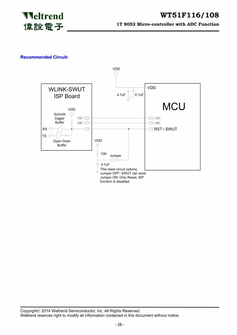
RReeccoommmmeennddeedd CCiirrccuuiitt::
0.1uF4.7uF
VDD
MCU
VDD
VDD
10K
4.7uF
RST / SWUT
Jumper
WLINK-SWUTISP Board
Open DrainBuffer
This reset circuit options. Jumper OFF: SWUT can workJumper ON: Only Reset, ISP function is disabled.
RX
TX
VDD
GND
VDD
GND
VDD
Schmitt triggerBuffer
WT51F116/108 1T 8052 Micro-controller with ADC Function
Copyright 2014 Weltrend Semiconductor, Inc. All Rights Reserved. Weltrend reserves right to modify all information contained in this document without notice.
- 29 -
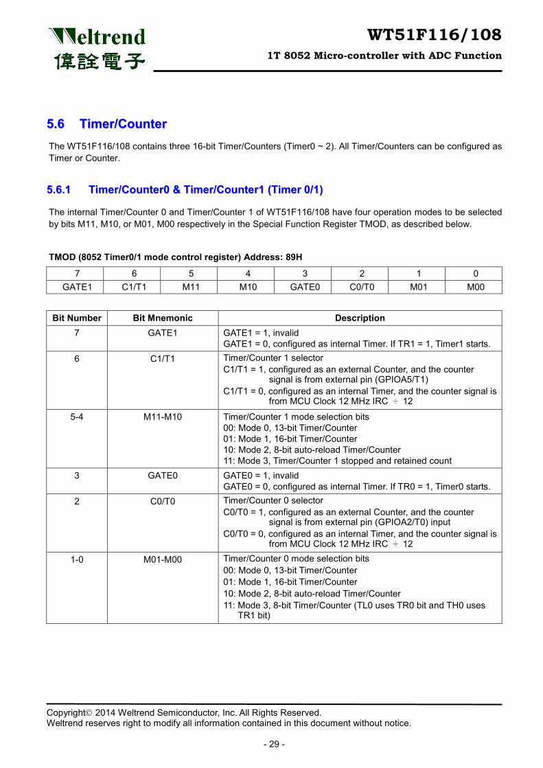
55..66 TTiimmeerr//CCoouunntteerr The WT51F116/108 contains three 16-bit Timer/Counters (Timer0 ~ 2). All Timer/Counters can be configured as Timer or Counter.
55..66..11 TTiimmeerr//CCoouunntteerr00 && TTiimmeerr//CCoouunntteerr11 ((TTiimmeerr 00//11))
The internal Timer/Counter 0 and Timer/Counter 1 of WT51F116/108 have four operation modes to be selected by bits M11, M10, or M01, M00 respectively in the Special Function Register TMOD, as described below.
TMOD (8052 Timer0/1 mode control register) Address: 89H
7 6 5 4 3 2 1 0 GATE1 C1/T1 M11 M10 GATE0 C0/T0 M01 M00
Bit Number Bit Mnemonic Description 7 GATE1 GATE1 = 1, invalid
GATE1 = 0, configured as internal Timer. If TR1 = 1, Timer1 starts. 6 C1/T1 Timer/Counter 1 selector
C1/T1 = 1, configured as an external Counter, and the counter signal is from external pin (GPIOA5/T1)
C1/T1 = 0, configured as an internal Timer, and the counter signal is from MCU Clock 12 MHz IRC ÷ 12
5-4 M11-M10
Timer/Counter 1 mode selection bits 00: Mode 0, 13-bit Timer/Counter 01: Mode 1, 16-bit Timer/Counter 10: Mode 2, 8-bit auto-reload Timer/Counter 11: Mode 3, Timer/Counter 1 stopped and retained count
3 GATE0 GATE0 = 1, invalid GATE0 = 0, configured as internal Timer. If TR0 = 1, Timer0 starts.
2 C0/T0 Timer/Counter 0 selector C0/T0 = 1, configured as an external Counter, and the counter
signal is from external pin (GPIOA2/T0) input C0/T0 = 0, configured as an internal Timer, and the counter signal is
from MCU Clock 12 MHz IRC ÷ 12
1-0 M01-M00
Timer/Counter 0 mode selection bits 00: Mode 0, 13-bit Timer/Counter 01: Mode 1, 16-bit Timer/Counter 10: Mode 2, 8-bit auto-reload Timer/Counter 11: Mode 3, 8-bit Timer/Counter (TL0 uses TR0 bit and TH0 uses
TR1 bit)
WT51F116/108 1T 8052 Micro-controller with ADC Function
Copyright 2014 Weltrend Semiconductor, Inc. All Rights Reserved. Weltrend reserves right to modify all information contained in this document without notice.
- 30 -
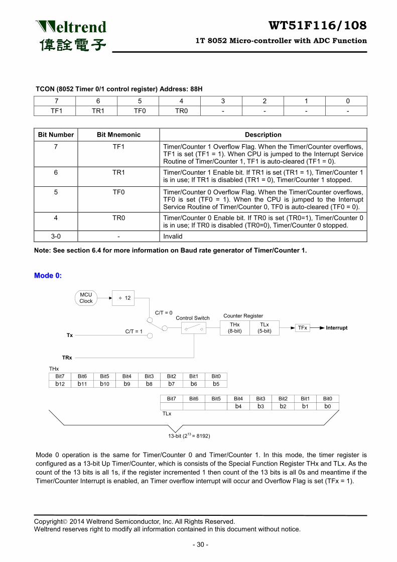
TCON (8052 Timer 0/1 control register) Address: 88H
7 6 5 4 3 2 1 0 TF1 TR1 TF0 TR0 - - - -
Bit Number Bit Mnemonic Description
7 TF1
Timer/Counter 1 Overflow Flag. When the Timer/Counter overflows, TF1 is set (TF1 = 1). When CPU is jumped to the Interrupt Service Routine of Timer/Counter 1, TF1 is auto-cleared (TF1 = 0).
6 TR1
Timer/Counter 1 Enable bit. If TR1 is set (TR1 = 1), Timer/Counter 1 is in use; If TR1 is disabled (TR1 = 0), Timer/Counter 1 stopped.
5 TF0 Timer/Counter 0 Overflow Flag. When the Timer/Counter overflows, TF0 is set (TF0 = 1). When the CPU is jumped to the Interrupt Service Routine of Timer/Counter 0, TF0 is auto-cleared (TF0 = 0).
4 TR0 Timer/Counter 0 Enable bit. If TR0 is set (TR0=1), Timer/Counter 0 is in use; If TR0 is disabled (TR0=0), Timer/Counter 0 stopped.
3-0 - Invalid
Note: See section 6.4 for more information on Baud rate generator of Timer/Counter 1.
MMooddee 00::
÷ 12MCU Clock
THx(8-bit)
TLx(5-bit) TFx
C/T = 0
C/T = 1Tx
Interrupt
TRx
Control Switch Counter Register
Bit7b12
Bit6b11
Bit5b10
Bit4b9
Bit3b8
Bit2b7
Bit1b6
Bit0b5
Bit3b3
Bit2b2
Bit1b1
Bit0b0
Bit7 Bit6 Bit5 Bit4b4
THx
TLx
13-bit (213 = 8192) Mode 0 operation is the same for Timer/Counter 0 and Timer/Counter 1. In this mode, the timer register is configured as a 13-bit Up Timer/Counter, which is consists of the Special Function Register THx and TLx. As the count of the 13 bits is all 1s, if the register incremented 1 then count of the 13 bits is all 0s and meantime if the Timer/Counter Interrupt is enabled, an Timer overflow interrupt will occur and Overflow Flag is set (TFx = 1).
WT51F116/108 1T 8052 Micro-controller with ADC Function
Copyright 2014 Weltrend Semiconductor, Inc. All Rights Reserved. Weltrend reserves right to modify all information contained in this document without notice.
- 31 -
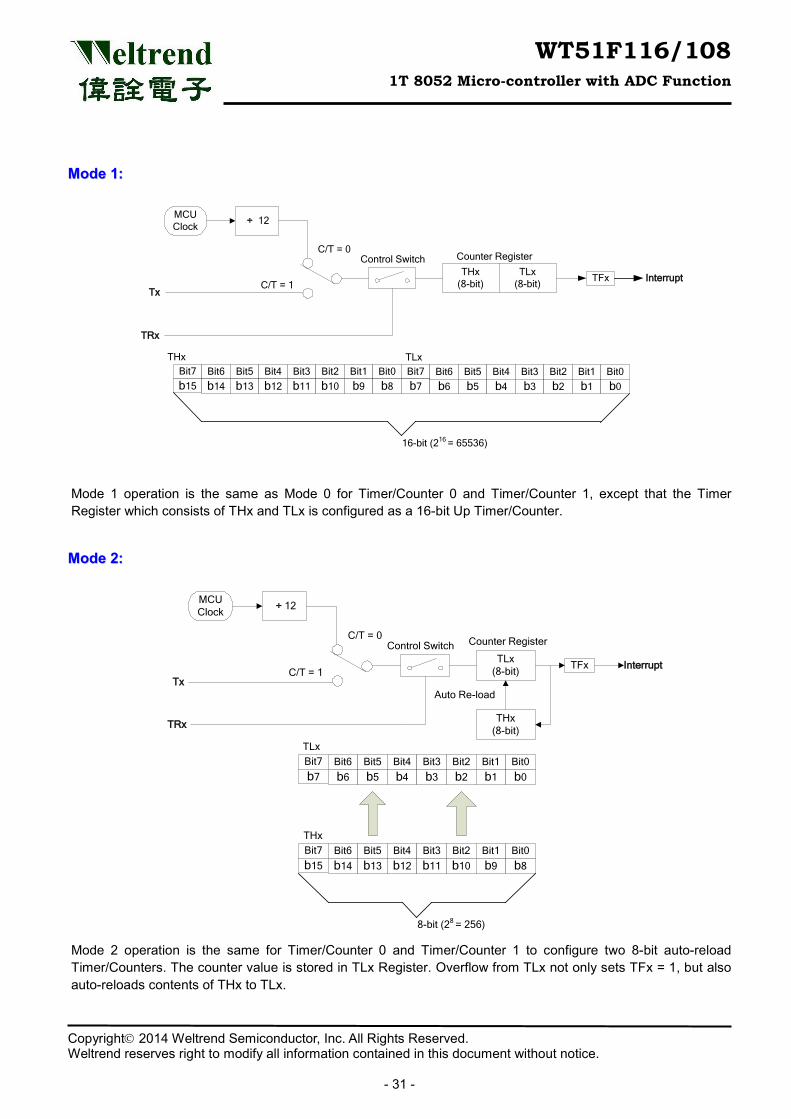
MMooddee 11::
÷ 12MCU Clock
THx(8-bit)
TLx(8-bit)
TFx
C/T = 0
C/T = 1Tx
Interrupt
TRx
Control Switch Counter Register
Bit7
b15
Bit6
b14
Bit5
b13
Bit4
b12
Bit3
b11
Bit2
b10
Bit1
b9
Bit0
b8
THx TLx
16-bit (216 = 65536)
Bit7
b7
Bit6
b6
Bit5
b5
Bit4
b4
Bit3
b3
Bit2
b2
Bit1
b1
Bit0
b0
Mode 1 operation is the same as Mode 0 for Timer/Counter 0 and Timer/Counter 1, except that the Timer Register which consists of THx and TLx is configured as a 16-bit Up Timer/Counter.
MMooddee 22::
÷ 12MCU Clock
THx(8-bit)
TLx(8-bit)
TFx
C/T = 0
C/T = 1Tx
Interrupt
TRx
Control Switch Counter Register
Bit7
b15
Bit6
b14
Bit5
b13
Bit4
b12
Bit3
b11
Bit2
b10
Bit1
b9
Bit0
b8
THx
TLx
8-bit (28 = 256)
Bit7
b7
Bit6
b6
Bit5
b5
Bit4
b4
Bit3
b3
Bit2
b2
Bit1
b1
Bit0
b0
Auto Re-load
Mode 2 operation is the same for Timer/Counter 0 and Timer/Counter 1 to configure two 8-bit auto-reload Timer/Counters. The counter value is stored in TLx Register. Overflow from TLx not only sets TFx = 1, but also auto-reloads contents of THx to TLx.
WT51F116/108 1T 8052 Micro-controller with ADC Function
Copyright 2014 Weltrend Semiconductor, Inc. All Rights Reserved. Weltrend reserves right to modify all information contained in this document without notice.
- 32 -
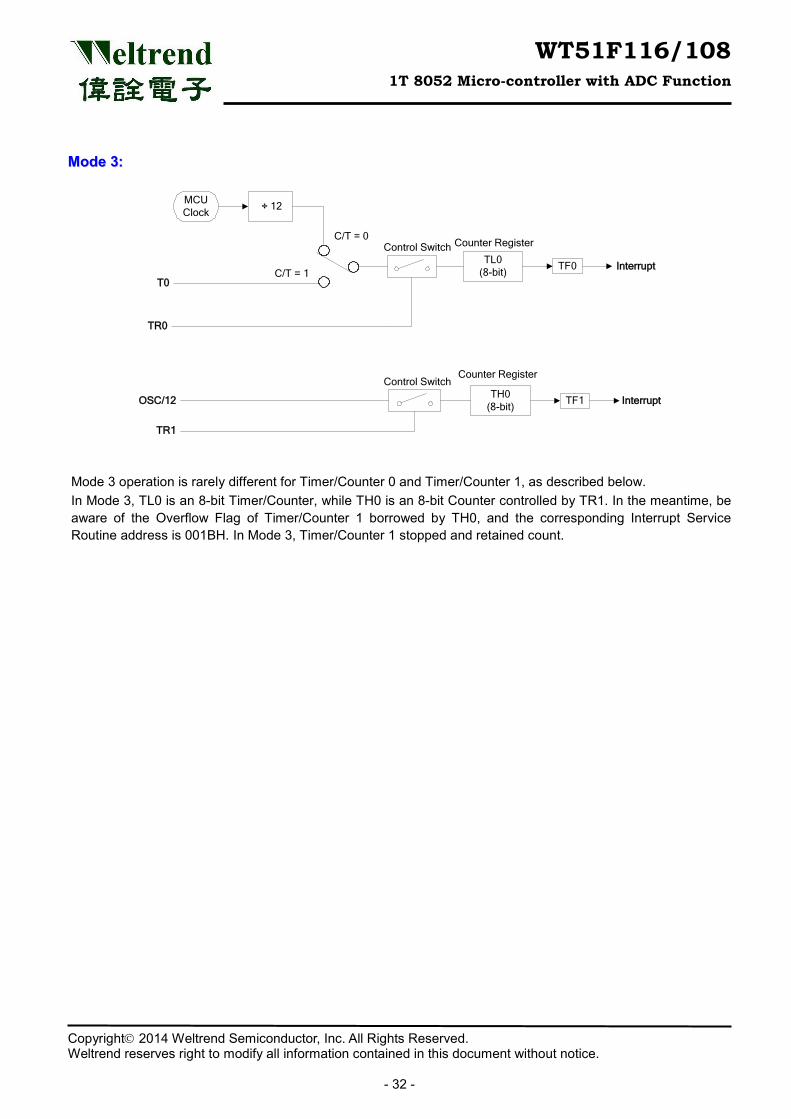
MMooddee 33::
÷ 12MCU Clock
TH0(8-bit)
TL0(8-bit)
TF0
C/T = 0
C/T = 1T0
Interrupt
TR0
Control Switch Counter Register
TR1
OSC/12 TF1 Interrupt
Control SwitchCounter Register
Mode 3 operation is rarely different for Timer/Counter 0 and Timer/Counter 1, as described below. In Mode 3, TL0 is an 8-bit Timer/Counter, while TH0 is an 8-bit Counter controlled by TR1. In the meantime, be aware of the Overflow Flag of Timer/Counter 1 borrowed by TH0, and the corresponding Interrupt Service Routine address is 001BH. In Mode 3, Timer/Counter 1 stopped and retained count.
WT51F116/108 1T 8052 Micro-controller with ADC Function
Copyright 2014 Weltrend Semiconductor, Inc. All Rights Reserved. Weltrend reserves right to modify all information contained in this document without notice.
- 33 -
55..66..22 TTiimmeerr//CCoouunntteerr 22 ((TTiimmeerr 22))
The WT51F116/108 internal Timer/Counter 2 is a 16-bit Timer/Counter. The timer/counter function can be selected by the C2/T2 bit in the Special Function Register T2CON, and the operating modes are selected by the RCLK, TCLK, CP/RL2, and TR2 bits in T2CON.
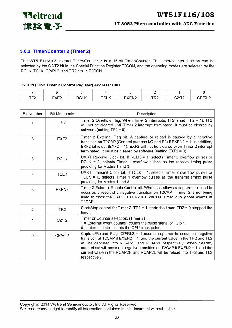
T2CON (8052 Timer 2 Control Register) Address: C8H
7 6 5 4 3 2 1 0 TF2 EXF2 RCLK TCLK EXEN2 TR2 C2/T2 CP/RL2
Bit Number Bit Mnemonic Description
7 TF2
Timer 2 Overflow Flag. When Timer 2 interrupts, TF2 is set (TF2 = 1); TF2 will not be cleared until Timer 2 interrupt terminated. It must be cleared by software (setting TF2 = 0).
6 EXF2 Timer 2 External Flag bit. A capture or reload is caused by a negative transition on T2CAP (General purpose I/O port F2) if EXEN2 = 1. In addition, EXF2 bit is set (EXF2 = 1), EXF2 will not be cleared even Timer 2 interrupt terminated. It must be cleared by software (setting EXF2 = 0).
5 RCLK UART Receive Clock bit. If RCLK = 1, selects Timer 2 overflow pulses or RCLK = 0, selects Timer 1 overflow pulses as the receive timing pulse providing for Modes 1 and 3.
4 TCLK UART Transmit Clock bit. If TCLK = 1, selects Timer 2 overflow pulses or TCLK = 0, selects Timer 1 overflow pulses as the transmit timing pulse providing for Modes 1 and 3.
3 EXEN2 Timer 2 External Enable Control bit. When set, allows a capture or reload to occur as a result of a negative transition on T2CAP if Timer 2 is not being used to clock the UART. EXEN2 = 0 causes Timer 2 to ignore events at T2CAP.
2 TR2 Start/Stop control for Timer 2. TR2 = 1 starts the timer. TR2 = 0 stopped the timer.
1 C2/T2 Timer or Counter select bit. (Timer 2) 1 = External event counter, counts the pulse signal of T2 pin. 0 = Internal timer, counts the CPU clock pulse
0 CP/RL2 Capture/Reload Flag. CP/RL2 = 1 causes captures to occur on negative transition at T2CAP if EXEN2 = 1, and the current value in the TH2 and TL2 will be captured into RCAP2H and RCAP2L respectively. When cleared, auto reload will occur on negative transition on T2CAP if EXEN2 = 1, and the current value in the RCAP2H and RCAP2L will be reload into TH2 and TL2 respectively.
WT51F116/108 1T 8052 Micro-controller with ADC Function
Copyright 2014 Weltrend Semiconductor, Inc. All Rights Reserved. Weltrend reserves right to modify all information contained in this document without notice.
- 34 -
Timer/Counter 2 Operating Modes
RCLK TCLK CP/RL2 T2OE Description
0 0 0 1 16-bit Auto-Reload mode
0 1 1 1 16-bit Capture mode (this mode is not available due to no T2 & T2CAP input pins)
1 X X 1 Baud Rate Generator
X 1
X X X 0 No action
Note: Refer to section 6.4 for more information about Timer/Counter 2 Baud Rate Generator.
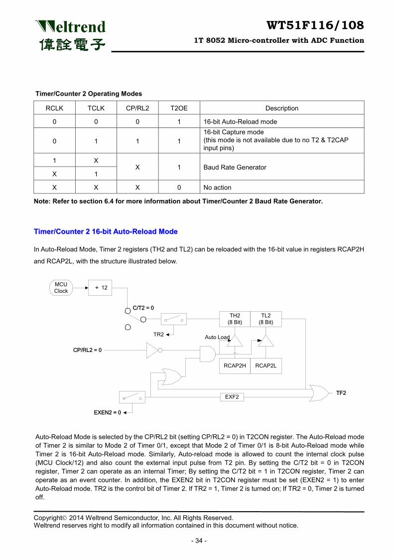
TTiimmeerr//CCoouunntteerr 22 1166--bbiitt AAuuttoo--RReellooaadd MMooddee
In Auto-Reload Mode, Timer 2 registers (TH2 and TL2) can be reloaded with the 16-bit value in registers RCAP2H
and RCAP2L, with the structure illustrated below.
÷ 12MCU Clock
TH2(8 Bit)
TL2(8 Bit)
RCAP2H RCAP2L
Auto Load
EXF2
TR2
EXEN2 = 0
C/T2 = 0
TF2
CP/RL2 = 0
Auto-Reload Mode is selected by the CP/RL2 bit (setting CP/RL2 = 0) in T2CON register. The Auto-Reload mode of Timer 2 is similar to Mode 2 of Timer 0/1, except that Mode 2 of Timer 0/1 is 8-bit Auto-Reload mode while Timer 2 is 16-bit Auto-Reload mode. Similarly, Auto-reload mode is allowed to count the internal clock pulse (MCU Clock/12) and also count the external input pulse from T2 pin. By setting the C/T2 bit = 0 in T2CON register, Timer 2 can operate as an internal Timer; By setting the C/T2 bit = 1 in T2CON register, Timer 2 can operate as an event counter. In addition, the EXEN2 bit in T2CON register must be set (EXEN2 = 1) to enter Auto-Reload mode. TR2 is the control bit of Timer 2. If TR2 = 1, Timer 2 is turned on; If TR2 = 0, Timer 2 is turned off.
WT51F116/108 1T 8052 Micro-controller with ADC Function
Copyright 2014 Weltrend Semiconductor, Inc. All Rights Reserved. Weltrend reserves right to modify all information contained in this document without notice.
- 35 -
55..77 RReesseett The WT51F116/108 has seven reset generation sources: Power On Reset (POR), Low Voltage Reset (LVR), Low Voltage Detection Reset (LVDR), External NRST Pin Reset, Watchdog Reset, ISP/ICE Command Reset, and PC Counter Overflow Reset (PC_OVR). During Reset, all registers are reset to their initial values. You may judge what kind of reset is generated by Reset Flag Register (XFR 0x03).
Power-on Reset (POR)
The Power-on Reset occurs when the VDD supply voltage is below the Power-on Reset voltage threshold (refer to DC Characteristics sections for more details), then XFR: 0x03 POR_RST_FLG = 1.
Low Voltage Reset (LVR)
A reset occurs when the VDD voltage is below the operating voltage threshold, then XFR: 0x03 LVR_RST_FLG = 1.
Low Voltage Detection Reset (LVDR)
A reset occurs when the VDD voltage is below the Low Voltage Detection setting level, then XFR: 0x03 LVD_RST_FLG = 1.
External NRST pin Reset
A reset occurs when the voltage of the external reset pin (NRST) is below its VIL (refer to DC characteristics sections for more details), then XFR: 0x03 NRST_FLG = 1.
Watchdog Timer Reset
A reset occurs when the Watchdog Timer times out, then XFR: 0x03 WDT_RST_FLG = 1.
ISP/ICE Command Reset
An ISP/ICE reset occurs when SWUT pin transmitted the reset command, then XFR: 0x03 ISP_RST_FLG = 1.
PC Counter Overflow Reset (PC_OVR)
The PC counter stores the address where the current instruction locates. A reset occurs when the address exceeds the range of the Flash memory (Flash Address 0x0000 ~ 0x3FFF), then XFR: 0x03 PC_OVL_RST_FLG = 1.
WT51F116/108 1T 8052 Micro-controller with ADC Function
Copyright 2014 Weltrend Semiconductor, Inc. All Rights Reserved. Weltrend reserves right to modify all information contained in this document without notice.
- 36 -
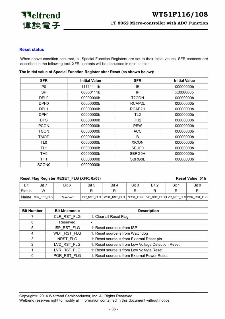
RReesseett ssttaattuuss
When above condition occurred, all Special Function Registers are set to their initial values. SFR contents are described in the following text. XFR contents will be discussed in next section.
The initial value of Special Function Register after Reset (as shown below):
SFR Initial Value SFR Initial Value P0 11111111b IE 00000000b SP 00000111b IP xx000000b
DPL0 00000000b T2CON 00000000b DPH0 00000000b RCAP2L 00000000b DPL1 00000000b RCAP2H 00000000b DPH1 00000000b TL2 00000000b DPS 00000000b TH2 00000000b
PCON 00000000b PSW 00000000b TCON 00000000b ACC 00000000b TMOD 00000000b B 00000000b
TL0 00000000b XICON 00000000b TL1 00000000b SBUF0 00000000b TH0 00000000b SBRG0H 00000000b TH1 00000000b SBRG0L 00000000b
SCON0 00000000b
Reset Flag Register RESET_FLG (XFR: 0x03) Reset Value: 01h
Bit Bit 7 Bit 6 Bit 5 Bit 4 Bit 3 Bit 2 Bit 1 Bit 0 Status W - R R R R R R Name CLR_RST_FLG Reserved ISP_RST_FLG WDT_RST_FLG NRST_FLG LVD_RST_FLG LVR_RST_FLG POR_RST_FLG
Bit Number Bit Mnemonic Description 7 CLR_RST_FLG 1: Clear all Reset Flag 6 Reserved - 5 ISP_RST_FLG 1: Reset source is from ISP 4 WDT_RST_FLG 1: Reset source is from Watchdog 3 NRST_FLG 1: Reset source is from External Reset pin 2 LVD_RST_FLG 1: Reset source is from Low Voltage Detection Reset 1 LVR_RST_FLG 1: Reset source is from Low Voltage Reset 0 POR_RST_FLG 1: Reset source is from External Power Reset
WT51F116/108 1T 8052 Micro-controller with ADC Function
Copyright 2014 Weltrend Semiconductor, Inc. All Rights Reserved. Weltrend reserves right to modify all information contained in this document without notice.
- 37 -
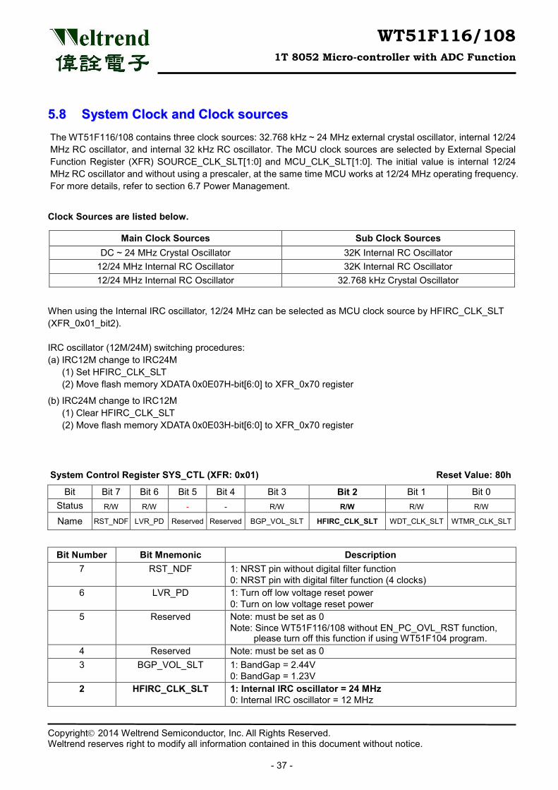
55..88 SSyysstteemm CClloocckk aanndd CClloocckk ssoouurrcceess The WT51F116/108 contains three clock sources: 32.768 kHz ~ 24 MHz external crystal oscillator, internal 12/24 MHz RC oscillator, and internal 32 kHz RC oscillator. The MCU clock sources are selected by External Special Function Register (XFR) SOURCE_CLK_SLT[1:0] and MCU_CLK_SLT[1:0]. The initial value is internal 12/24 MHz RC oscillator and without using a prescaler, at the same time MCU works at 12/24 MHz operating frequency. For more details, refer to section 6.7 Power Management.
Clock Sources are listed below.
Main Clock Sources Sub Clock Sources DC ~ 24 MHz Crystal Oscillator 32K Internal RC Oscillator
12/24 MHz Internal RC Oscillator 32K Internal RC Oscillator 12/24 MHz Internal RC Oscillator 32.768 kHz Crystal Oscillator
When using the Internal IRC oscillator, 12/24 MHz can be selected as MCU clock source by HFIRC_CLK_SLT (XFR_0x01_bit2). IRC oscillator (12M/24M) switching procedures: (a) IRC12M change to IRC24M (1) Set HFIRC_CLK_SLT (2) Move flash memory XDATA 0x0E07H-bit[6:0] to XFR_0x70 register
(b) IRC24M change to IRC12M (1) Clear HFIRC_CLK_SLT (2) Move flash memory XDATA 0x0E03H-bit[6:0] to XFR_0x70 register
System Control Register SYS_CTL (XFR: 0x01) Reset Value: 80h
Bit Bit 7 Bit 6 Bit 5 Bit 4 Bit 3 Bit 2 Bit 1 Bit 0 Status R/W R/W - - R/W R/W R/W R/W
Name RST_NDF LVR_PD Reserved Reserved BGP_VOL_SLT HFIRC_CLK_SLT WDT_CLK_SLT WTMR_CLK_SLT
Bit Number Bit Mnemonic Description 7 RST_NDF 1: NRST pin without digital filter function
0: NRST pin with digital filter function (4 clocks) 6 LVR_PD 1: Turn off low voltage reset power
0: Turn on low voltage reset power 5 Reserved Note: must be set as 0
Note: Since WT51F116/108 without EN_PC_OVL_RST function, please turn off this function if using WT51F104 program.
4 Reserved Note: must be set as 0 3 BGP_VOL_SLT 1: BandGap = 2.44V
0: BandGap = 1.23V 2 HFIRC_CLK_SLT 1: Internal IRC oscillator = 24 MHz
0: Internal IRC oscillator = 12 MHz
WT51F116/108 1T 8052 Micro-controller with ADC Function
Copyright 2014 Weltrend Semiconductor, Inc. All Rights Reserved. Weltrend reserves right to modify all information contained in this document without notice.
- 38 -
Bit Number Bit Mnemonic Description 1 WDT_CLK_SLT 1: Watchdog Timer uses external 24 MHz ~ 32 kHz crystal oscillator
0: Watchdog Timer uses internal 32 kHz RC oscillator 0 WTMR_CLK_SLT 1: Watch Timer uses external 24 MHz ~ 32 kHz crystal oscillator
0: Watch Timer uses internal 32 kHz RC oscillator -: unimplemented.
WT51F116/108 1T 8052 Micro-controller with ADC Function
Copyright 2014 Weltrend Semiconductor, Inc. All Rights Reserved. Weltrend reserves right to modify all information contained in this document without notice.
- 39 -
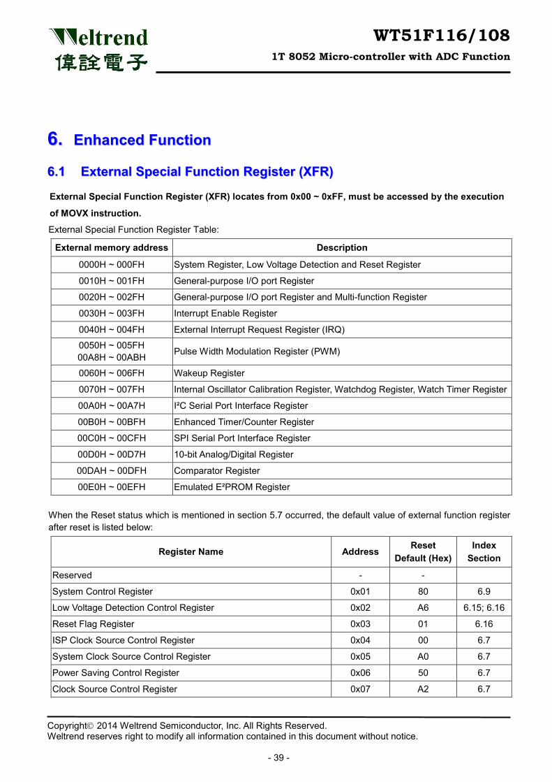
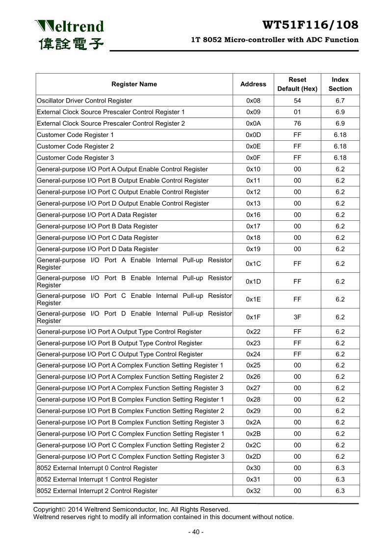
66..11 EExxtteerrnnaall SSppeecciiaall FFuunnccttiioonn RReeggiisstteerr ((XXFFRR))
External Special Function Register (XFR) locates from 0x00 ~ 0xFF, must be accessed by the execution
of MOVX instruction.
External Special Function Register Table:
External memory address Description
0000H ~ 000FH System Register, Low Voltage Detection and Reset Register
0010H ~ 001FH General-purpose I/O port Register
0020H ~ 002FH General-purpose I/O port Register and Multi-function Register
0030H ~ 003FH Interrupt Enable Register
0040H ~ 004FH External Interrupt Request Register (IRQ)
0050H ~ 005FH 00A8H ~ 00ABH Pulse Width Modulation Register (PWM)
0060H ~ 006FH Wakeup Register
0070H ~ 007FH Internal Oscillator Calibration Register, Watchdog Register, Watch Timer Register
00A0H ~ 00A7H I²C Serial Port Interface Register
00B0H ~ 00BFH Enhanced Timer/Counter Register
00C0H ~ 00CFH SPI Serial Port Interface Register
00D0H ~ 00D7H 10-bit Analog/Digital Register
00DAH ~ 00DFH Comparator Register
00E0H ~ 00EFH Emulated E²PROM Register When the Reset status which is mentioned in section 5.7 occurred, the default value of external function register after reset is listed below:
Register Name Address Reset Default (Hex)
Index Section
Reserved - -
System Control Register 0x01 80 6.9
Low Voltage Detection Control Register 0x02 A6 6.15; 6.16
Reset Flag Register 0x03 01 6.16
ISP Clock Source Control Register 0x04 00 6.7
System Clock Source Control Register 0x05 A0 6.7
Power Saving Control Register 0x06 50 6.7
Clock Source Control Register 0x07 A2 6.7
66.. EEnnhhaanncceedd FFuunnccttiioonn
WT51F116/108 1T 8052 Micro-controller with ADC Function
Copyright 2014 Weltrend Semiconductor, Inc. All Rights Reserved. Weltrend reserves right to modify all information contained in this document without notice.
- 40 -
Register Name Address Reset Default (Hex)
Index Section
Oscillator Driver Control Register 0x08 54 6.7
External Clock Source Prescaler Control Register 1 0x09 01 6.9
External Clock Source Prescaler Control Register 2 0x0A 76 6.9
Customer Code Register 1 0x0D FF 6.18
Customer Code Register 2 0x0E FF 6.18
Customer Code Register 3 0x0F FF 6.18
General-purpose I/O Port A Output Enable Control Register 0x10 00 6.2
General-purpose I/O Port B Output Enable Control Register 0x11 00 6.2
General-purpose I/O Port C Output Enable Control Register 0x12 00 6.2
General-purpose I/O Port D Output Enable Control Register 0x13 00 6.2
General-purpose I/O Port A Data Register 0x16 00 6.2
General-purpose I/O Port B Data Register 0x17 00 6.2
General-purpose I/O Port C Data Register 0x18 00 6.2
General-purpose I/O Port D Data Register 0x19 00 6.2
General-purpose I/O Port A Enable Internal Pull-up Resistor Register 0x1C FF 6.2
General-purpose I/O Port B Enable Internal Pull-up Resistor Register 0x1D FF 6.2
General-purpose I/O Port C Enable Internal Pull-up Resistor Register 0x1E FF 6.2
General-purpose I/O Port D Enable Internal Pull-up Resistor Register 0x1F 3F 6.2
General-purpose I/O Port A Output Type Control Register 0x22 FF 6.2
General-purpose I/O Port B Output Type Control Register 0x23 FF 6.2
General-purpose I/O Port C Output Type Control Register 0x24 FF 6.2
General-purpose I/O Port A Complex Function Setting Register 1 0x25 00 6.2
General-purpose I/O Port A Complex Function Setting Register 2 0x26 00 6.2
General-purpose I/O Port A Complex Function Setting Register 3 0x27 00 6.2
General-purpose I/O Port B Complex Function Setting Register 1 0x28 00 6.2
General-purpose I/O Port B Complex Function Setting Register 2 0x29 00 6.2
General-purpose I/O Port B Complex Function Setting Register 3 0x2A 00 6.2
General-purpose I/O Port C Complex Function Setting Register 1 0x2B 00 6.2
General-purpose I/O Port C Complex Function Setting Register 2 0x2C 00 6.2
General-purpose I/O Port C Complex Function Setting Register 3 0x2D 00 6.2
8052 External Interrupt 0 Control Register 0x30 00 6.3
8052 External Interrupt 1 Control Register 0x31 00 6.3
8052 External Interrupt 2 Control Register 0x32 00 6.3
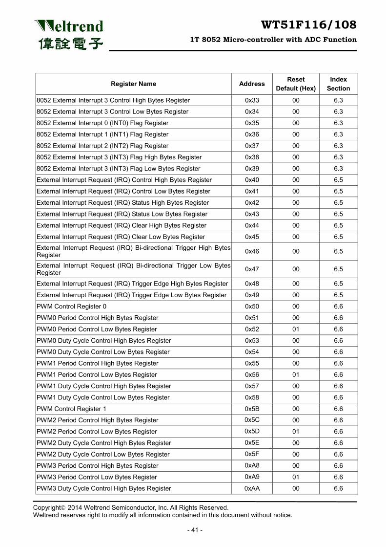
WT51F116/108 1T 8052 Micro-controller with ADC Function
Copyright 2014 Weltrend Semiconductor, Inc. All Rights Reserved. Weltrend reserves right to modify all information contained in this document without notice.
- 41 -
Register Name Address Reset Default (Hex)
Index Section
8052 External Interrupt 3 Control High Bytes Register 0x33 00 6.3
8052 External Interrupt 3 Control Low Bytes Register 0x34 00 6.3
8052 External Interrupt 0 (INT0) Flag Register 0x35 00 6.3
8052 External Interrupt 1 (INT1) Flag Register 0x36 00 6.3
8052 External Interrupt 2 (INT2) Flag Register 0x37 00 6.3
8052 External Interrupt 3 (INT3) Flag High Bytes Register 0x38 00 6.3
8052 External Interrupt 3 (INT3) Flag Low Bytes Register 0x39 00 6.3
External Interrupt Request (IRQ) Control High Bytes Register 0x40 00 6.5
External Interrupt Request (IRQ) Control Low Bytes Register 0x41 00 6.5
External Interrupt Request (IRQ) Status High Bytes Register 0x42 00 6.5
External Interrupt Request (IRQ) Status Low Bytes Register 0x43 00 6.5
External Interrupt Request (IRQ) Clear High Bytes Register 0x44 00 6.5
External Interrupt Request (IRQ) Clear Low Bytes Register 0x45 00 6.5
External Interrupt Request (IRQ) Bi-directional Trigger High Bytes Register 0x46 00 6.5
External Interrupt Request (IRQ) Bi-directional Trigger Low Bytes Register 0x47 00 6.5
External Interrupt Request (IRQ) Trigger Edge High Bytes Register 0x48 00 6.5
External Interrupt Request (IRQ) Trigger Edge Low Bytes Register 0x49 00 6.5
PWM Control Register 0 0x50 00 6.6
PWM0 Period Control High Bytes Register 0x51 00 6.6
PWM0 Period Control Low Bytes Register 0x52 01 6.6
PWM0 Duty Cycle Control High Bytes Register 0x53 00 6.6
PWM0 Duty Cycle Control Low Bytes Register 0x54 00 6.6
PWM1 Period Control High Bytes Register 0x55 00 6.6
PWM1 Period Control Low Bytes Register 0x56 01 6.6
PWM1 Duty Cycle Control High Bytes Register 0x57 00 6.6
PWM1 Duty Cycle Control Low Bytes Register 0x58 00 6.6
PWM Control Register 1 0x5B 00 6.6
PWM2 Period Control High Bytes Register 0x5C 00 6.6
PWM2 Period Control Low Bytes Register 0x5D 01 6.6
PWM2 Duty Cycle Control High Bytes Register 0x5E 00 6.6
PWM2 Duty Cycle Control Low Bytes Register 0x5F 00 6.6
PWM3 Period Control High Bytes Register 0xA8 00 6.6
PWM3 Period Control Low Bytes Register 0xA9 01 6.6
PWM3 Duty Cycle Control High Bytes Register 0xAA 00 6.6
WT51F116/108 1T 8052 Micro-controller with ADC Function
Copyright 2014 Weltrend Semiconductor, Inc. All Rights Reserved. Weltrend reserves right to modify all information contained in this document without notice.
- 42 -
Register Name Address Reset Default (Hex)
Index Section
PWM3 Duty Cycle Control Low Bytes Register 0xAB 00 6.6
General-purpose I/O Port A Wakeup Control Register 0x60 00 6.7
General-purpose I/O Port B Wakeup Control Register 0x61 00 6.7
General-purpose I/O Port C Wakeup Control Register 0x62 00 6.7
Peripheral Interrupt Wakeup Control Register 0x64 00 6.7
General-purpose I/O Port A Wakeup Flag Register 0x65 00 6.7
General-purpose I/O Port B Wakeup Flag Register 0x66 00 6.7
General-purpose I/O Port C Wakeup Flag Register 0x67 00 6.7
Peripheral Interrupt Wakeup Flag Register 0x69 00 6.7
Wakeup Clear Register 0x6A 00 6.7
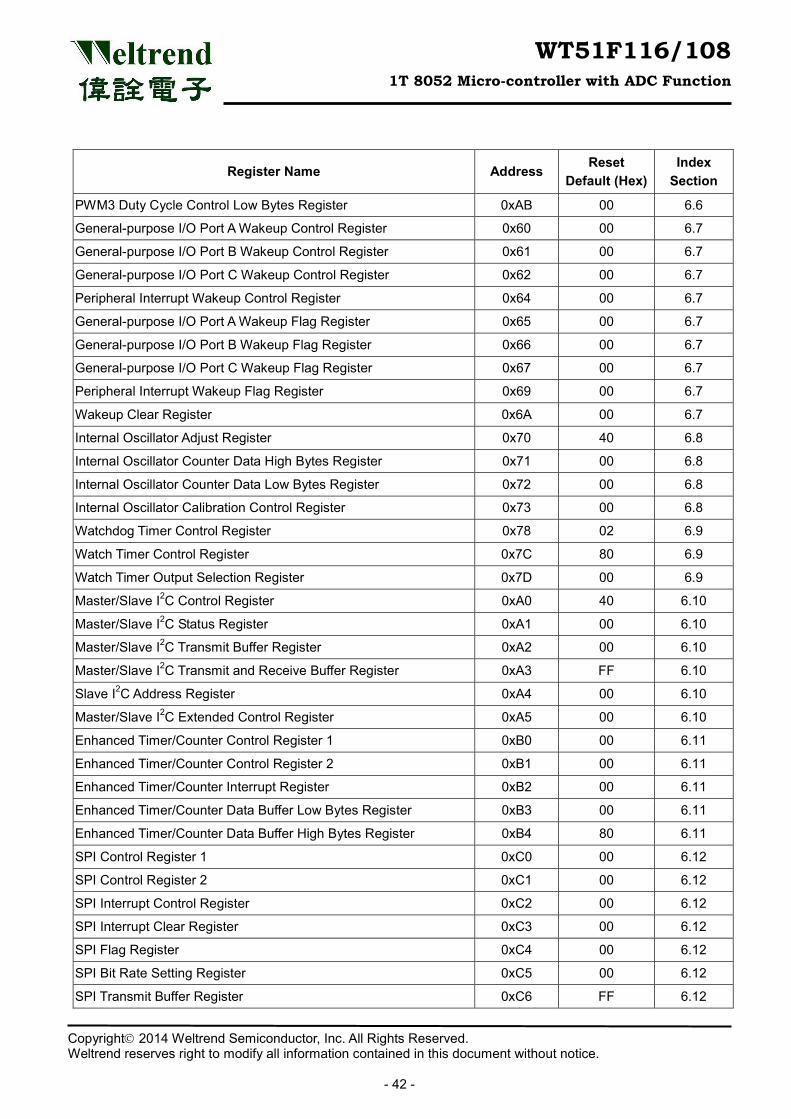
Internal Oscillator Adjust Register 0x70 40 6.8
Internal Oscillator Counter Data High Bytes Register 0x71 00 6.8
Internal Oscillator Counter Data Low Bytes Register 0x72 00 6.8
Internal Oscillator Calibration Control Register 0x73 00 6.8
Watchdog Timer Control Register 0x78 02 6.9
Watch Timer Control Register 0x7C 80 6.9
Watch Timer Output Selection Register 0x7D 00 6.9
Master/Slave I2C Control Register 0xA0 40 6.10
Master/Slave I2C Status Register 0xA1 00 6.10
Master/Slave I2C Transmit Buffer Register 0xA2 00 6.10
Master/Slave I2C Transmit and Receive Buffer Register 0xA3 FF 6.10
Slave I2C Address Register 0xA4 00 6.10
Master/Slave I2C Extended Control Register 0xA5 00 6.10
Enhanced Timer/Counter Control Register 1 0xB0 00 6.11
Enhanced Timer/Counter Control Register 2 0xB1 00 6.11
Enhanced Timer/Counter Interrupt Register 0xB2 00 6.11
Enhanced Timer/Counter Data Buffer Low Bytes Register 0xB3 00 6.11
Enhanced Timer/Counter Data Buffer High Bytes Register 0xB4 80 6.11
SPI Control Register 1 0xC0 00 6.12
SPI Control Register 2 0xC1 00 6.12
SPI Interrupt Control Register 0xC2 00 6.12
SPI Interrupt Clear Register 0xC3 00 6.12
SPI Flag Register 0xC4 00 6.12
SPI Bit Rate Setting Register 0xC5 00 6.12
SPI Transmit Buffer Register 0xC6 FF 6.12
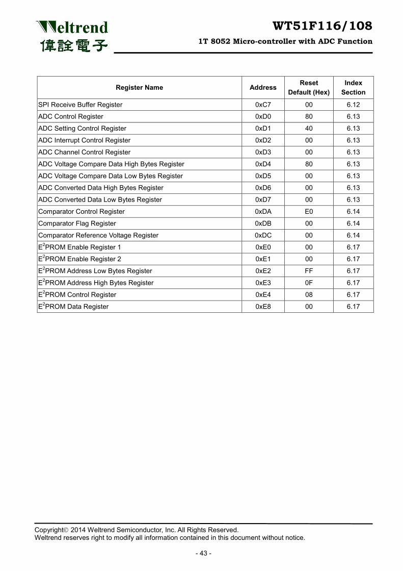
WT51F116/108 1T 8052 Micro-controller with ADC Function
Copyright 2014 Weltrend Semiconductor, Inc. All Rights Reserved. Weltrend reserves right to modify all information contained in this document without notice.
- 43 -
Register Name Address Reset Default (Hex)
Index Section
SPI Receive Buffer Register 0xC7 00 6.12
ADC Control Register 0xD0 80 6.13
ADC Setting Control Register 0xD1 40 6.13
ADC Interrupt Control Register 0xD2 00 6.13
ADC Channel Control Register 0xD3 00 6.13
ADC Voltage Compare Data High Bytes Register 0xD4 80 6.13
ADC Voltage Compare Data Low Bytes Register 0xD5 00 6.13
ADC Converted Data High Bytes Register 0xD6 00 6.13
ADC Converted Data Low Bytes Register 0xD7 00 6.13
Comparator Control Register 0xDA E0 6.14
Comparator Flag Register 0xDB 00 6.14
Comparator Reference Voltage Register 0xDC 00 6.14
E2PROM Enable Register 1 0xE0 00 6.17
E2PROM Enable Register 2 0xE1 00 6.17
E2PROM Address Low Bytes Register 0xE2 FF 6.17
E2PROM Address High Bytes Register 0xE3 0F 6.17
E2PROM Control Register 0xE4 08 6.17
E2PROM Data Register 0xE8 00 6.17
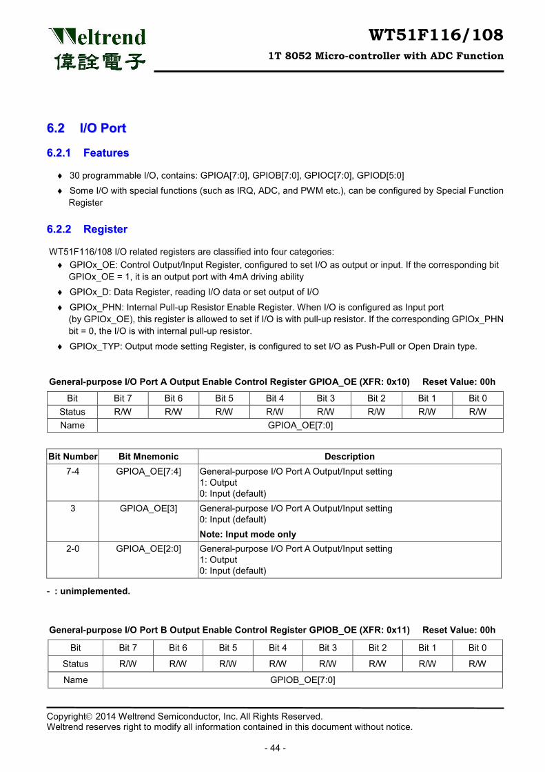
WT51F116/108 1T 8052 Micro-controller with ADC Function
Copyright 2014 Weltrend Semiconductor, Inc. All Rights Reserved. Weltrend reserves right to modify all information contained in this document without notice.
- 44 -
66..22 II//OO PPoorrtt
66..22..11 FFeeaattuurreess
♦ 30 programmable I/O, contains: GPIOA[7:0], GPIOB[7:0], GPIOC[7:0], GPIOD[5:0] ♦ Some I/O with special functions (such as IRQ, ADC, and PWM etc.), can be configured by Special Function
Register 66..22..22 RReeggiisstteerr
WT51F116/108 I/O related registers are classified into four categories: ♦ GPIOx_OE: Control Output/Input Register, configured to set I/O as output or input. If the corresponding bit
GPIOx_OE = 1, it is an output port with 4mA driving ability ♦ GPIOx_D: Data Register, reading I/O data or set output of I/O
♦ GPIOx_PHN: Internal Pull-up Resistor Enable Register. When I/O is configured as Input port (by GPIOx_OE), this register is allowed to set if I/O is with pull-up resistor. If the corresponding GPIOx_PHN bit = 0, the I/O is with internal pull-up resistor.
♦ GPIOx_TYP: Output mode setting Register, is configured to set I/O as Push-Pull or Open Drain type.
General-purpose I/O Port A Output Enable Control Register GPIOA_OE (XFR: 0x10) Reset Value: 00h
Bit Bit 7 Bit 6 Bit 5 Bit 4 Bit 3 Bit 2 Bit 1 Bit 0 Status R/W R/W R/W R/W R/W R/W R/W R/W Name GPIOA_OE[7:0]
Bit Number Bit Mnemonic Description 7-4 GPIOA_OE[7:4] General-purpose I/O Port A Output/Input setting
1: Output 0: Input (default)
3 GPIOA_OE[3] General-purpose I/O Port A Output/Input setting 0: Input (default) Note: Input mode only
2-0 GPIOA_OE[2:0] General-purpose I/O Port A Output/Input setting 1: Output 0: Input (default)
- : unimplemented.
General-purpose I/O Port B Output Enable Control Register GPIOB_OE (XFR: 0x11) Reset Value: 00h
Bit Bit 7 Bit 6 Bit 5 Bit 4 Bit 3 Bit 2 Bit 1 Bit 0
Status R/W R/W R/W R/W R/W R/W R/W R/W
Name GPIOB_OE[7:0]
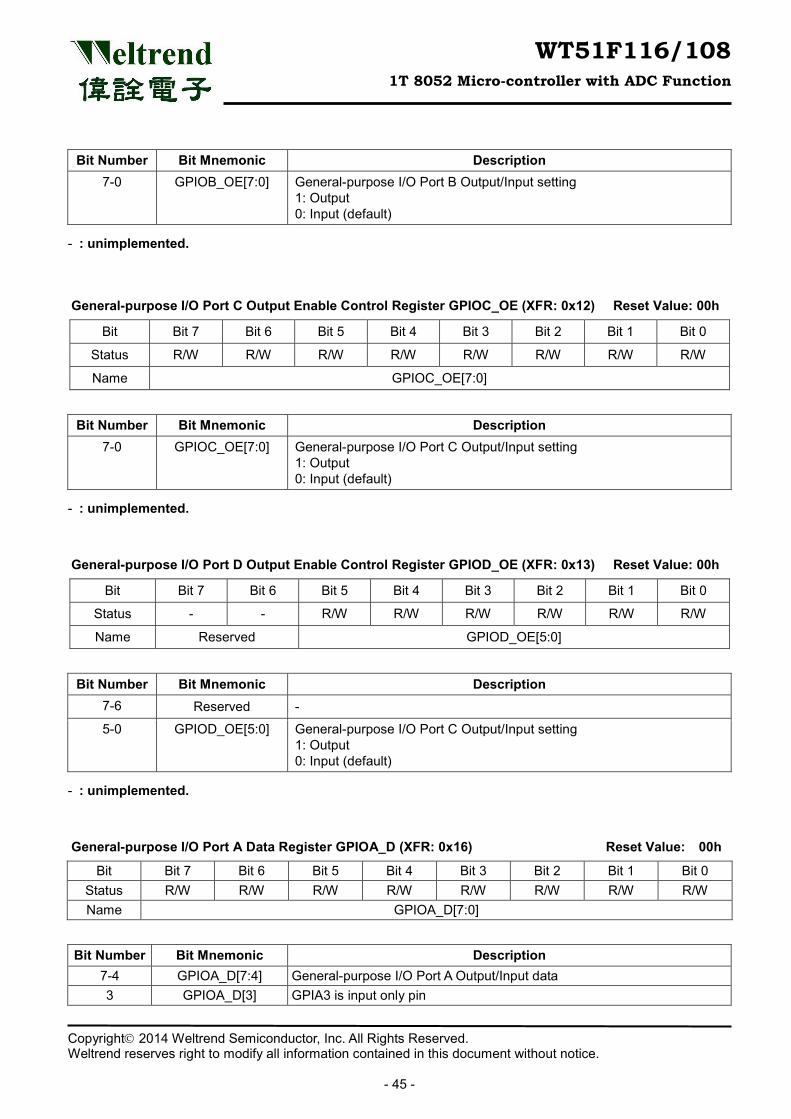
WT51F116/108 1T 8052 Micro-controller with ADC Function
Copyright 2014 Weltrend Semiconductor, Inc. All Rights Reserved. Weltrend reserves right to modify all information contained in this document without notice.
- 45 -
Bit Number Bit Mnemonic Description 7-0 GPIOB_OE[7:0] General-purpose I/O Port B Output/Input setting
1: Output 0: Input (default)
- : unimplemented.
General-purpose I/O Port C Output Enable Control Register GPIOC_OE (XFR: 0x12) Reset Value: 00h
Bit Bit 7 Bit 6 Bit 5 Bit 4 Bit 3 Bit 2 Bit 1 Bit 0
Status R/W R/W R/W R/W R/W R/W R/W R/W
Name GPIOC_OE[7:0]
Bit Number Bit Mnemonic Description 7-0 GPIOC_OE[7:0] General-purpose I/O Port C Output/Input setting
1: Output 0: Input (default)
- : unimplemented.
General-purpose I/O Port D Output Enable Control Register GPIOD_OE (XFR: 0x13) Reset Value: 00h
Bit Bit 7 Bit 6 Bit 5 Bit 4 Bit 3 Bit 2 Bit 1 Bit 0
Status - - R/W R/W R/W R/W R/W R/W
Name Reserved GPIOD_OE[5:0]
Bit Number Bit Mnemonic Description 7-6 Reserved -
5-0 GPIOD_OE[5:0] General-purpose I/O Port C Output/Input setting 1: Output 0: Input (default)
- : unimplemented.
General-purpose I/O Port A Data Register GPIOA_D (XFR: 0x16) Reset Value: 00h
Bit Bit 7 Bit 6 Bit 5 Bit 4 Bit 3 Bit 2 Bit 1 Bit 0 Status R/W R/W R/W R/W R/W R/W R/W R/W Name GPIOA_D[7:0]
Bit Number Bit Mnemonic Description 7-4 GPIOA_D[7:4] General-purpose I/O Port A Output/Input data 3 GPIOA_D[3] GPIA3 is input only pin
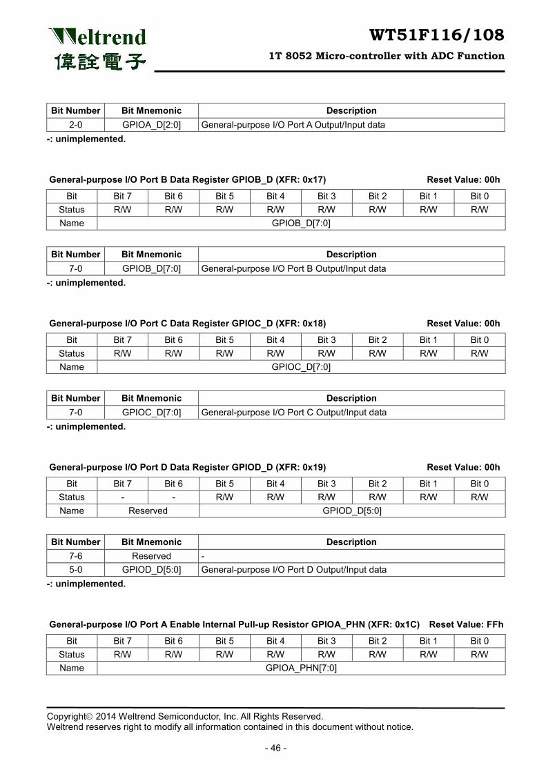
WT51F116/108 1T 8052 Micro-controller with ADC Function
Copyright 2014 Weltrend Semiconductor, Inc. All Rights Reserved. Weltrend reserves right to modify all information contained in this document without notice.
- 46 -
Bit Number Bit Mnemonic Description 2-0 GPIOA_D[2:0] General-purpose I/O Port A Output/Input data
-: unimplemented.
General-purpose I/O Port B Data Register GPIOB_D (XFR: 0x17) Reset Value: 00h
Bit Bit 7 Bit 6 Bit 5 Bit 4 Bit 3 Bit 2 Bit 1 Bit 0 Status R/W R/W R/W R/W R/W R/W R/W R/W Name GPIOB_D[7:0]
Bit Number Bit Mnemonic Description 7-0 GPIOB_D[7:0] General-purpose I/O Port B Output/Input data
-: unimplemented.
General-purpose I/O Port C Data Register GPIOC_D (XFR: 0x18) Reset Value: 00h
Bit Bit 7 Bit 6 Bit 5 Bit 4 Bit 3 Bit 2 Bit 1 Bit 0 Status R/W R/W R/W R/W R/W R/W R/W R/W Name GPIOC_D[7:0]
Bit Number Bit Mnemonic Description 7-0 GPIOC_D[7:0] General-purpose I/O Port C Output/Input data
-: unimplemented.
General-purpose I/O Port D Data Register GPIOD_D (XFR: 0x19) Reset Value: 00h
Bit Bit 7 Bit 6 Bit 5 Bit 4 Bit 3 Bit 2 Bit 1 Bit 0 Status - - R/W R/W R/W R/W R/W R/W Name Reserved GPIOD_D[5:0]
Bit Number Bit Mnemonic Description 7-6 Reserved - 5-0 GPIOD_D[5:0] General-purpose I/O Port D Output/Input data
-: unimplemented.
General-purpose I/O Port A Enable Internal Pull-up Resistor GPIOA_PHN (XFR: 0x1C) Reset Value: FFh
Bit Bit 7 Bit 6 Bit 5 Bit 4 Bit 3 Bit 2 Bit 1 Bit 0 Status R/W R/W R/W R/W R/W R/W R/W R/W Name GPIOA_PHN[7:0]
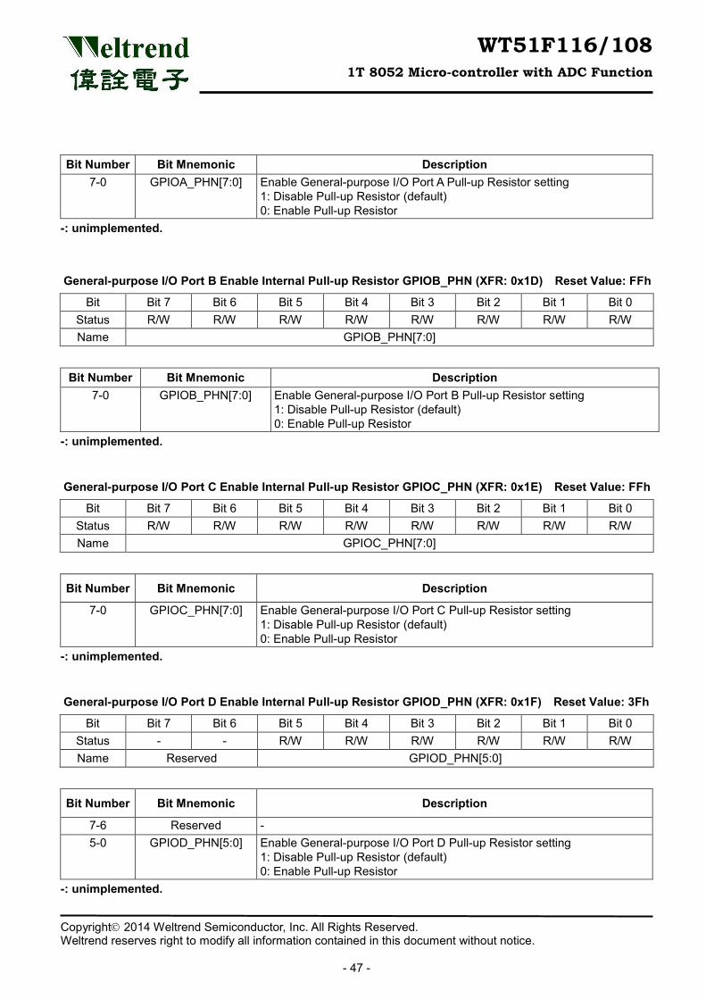
WT51F116/108 1T 8052 Micro-controller with ADC Function
Copyright 2014 Weltrend Semiconductor, Inc. All Rights Reserved. Weltrend reserves right to modify all information contained in this document without notice.
- 47 -
Bit Number Bit Mnemonic Description 7-0 GPIOA_PHN[7:0] Enable General-purpose I/O Port A Pull-up Resistor setting
1: Disable Pull-up Resistor (default) 0: Enable Pull-up Resistor
-: unimplemented.
General-purpose I/O Port B Enable Internal Pull-up Resistor GPIOB_PHN (XFR: 0x1D) Reset Value: FFh
Bit Bit 7 Bit 6 Bit 5 Bit 4 Bit 3 Bit 2 Bit 1 Bit 0 Status R/W R/W R/W R/W R/W R/W R/W R/W Name GPIOB_PHN[7:0]
Bit Number Bit Mnemonic Description 7-0 GPIOB_PHN[7:0] Enable General-purpose I/O Port B Pull-up Resistor setting
1: Disable Pull-up Resistor (default) 0: Enable Pull-up Resistor
-: unimplemented.
General-purpose I/O Port C Enable Internal Pull-up Resistor GPIOC_PHN (XFR: 0x1E) Reset Value: FFh
Bit Bit 7 Bit 6 Bit 5 Bit 4 Bit 3 Bit 2 Bit 1 Bit 0 Status R/W R/W R/W R/W R/W R/W R/W R/W Name GPIOC_PHN[7:0]
Bit Number Bit Mnemonic Description
7-0 GPIOC_PHN[7:0] Enable General-purpose I/O Port C Pull-up Resistor setting 1: Disable Pull-up Resistor (default) 0: Enable Pull-up Resistor
-: unimplemented.
General-purpose I/O Port D Enable Internal Pull-up Resistor GPIOD_PHN (XFR: 0x1F) Reset Value: 3Fh
Bit Bit 7 Bit 6 Bit 5 Bit 4 Bit 3 Bit 2 Bit 1 Bit 0 Status - - R/W R/W R/W R/W R/W R/W Name Reserved GPIOD_PHN[5:0]
Bit Number Bit Mnemonic Description
7-6 Reserved - 5-0 GPIOD_PHN[5:0] Enable General-purpose I/O Port D Pull-up Resistor setting
1: Disable Pull-up Resistor (default) 0: Enable Pull-up Resistor
-: unimplemented.
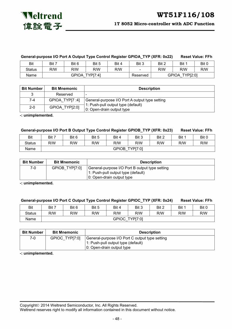
WT51F116/108 1T 8052 Micro-controller with ADC Function
Copyright 2014 Weltrend Semiconductor, Inc. All Rights Reserved. Weltrend reserves right to modify all information contained in this document without notice.
- 48 -
General-purpose I/O Port A Output Type Control Register GPIOA_TYP (XFR: 0x22) Reset Value: FFh
Bit Bit 7 Bit 6 Bit 5 Bit 4 Bit 3 Bit 2 Bit 1 Bit 0 Status R/W R/W R/W R/W - R/W R/W R/W Name GPIOA_TYP[7:4] Reserved GPIOA_TYP[2:0]
Bit Number Bit Mnemonic Description 3 Reserved -
7-4 GPIOA_TYP[7 :4] General-purpose I/O Port A output type setting 1: Push-pull output type (default) 0: Open-drain output type 2-0 GPIOA_TYP[2:0]
-: unimplemented.
General-purpose I/O Port B Output Type Control Register GPIOB_TYP (XFR: 0x23) Reset Value: FFh
Bit Bit 7 Bit 6 Bit 5 Bit 4 Bit 3 Bit 2 Bit 1 Bit 0 Status R/W R/W R/W R/W R/W R/W R/W R/W Name GPIOB_TYP[7:0]
Bit Number Bit Mnemonic Description 7-0 GPIOB_TYP[7:0] General-purpose I/O Port B output type setting
1: Push-pull output type (default) 0: Open-drain output type
-: unimplemented.
General-purpose I/O Port C Output Type Control Register GPIOC_TYP (XFR: 0x24) Reset Value: FFh
Bit Bit 7 Bit 6 Bit 5 Bit 4 Bit 3 Bit 2 Bit 1 Bit 0 Status R/W R/W R/W R/W R/W R/W R/W R/W Name GPIOC_TYP[7:0]
Bit Number Bit Mnemonic Description 7-0 GPIOC_TYP[7:0] General-purpose I/O Port C output type setting
1: Push-pull output type (default) 0: Open-drain output type
-: unimplemented.
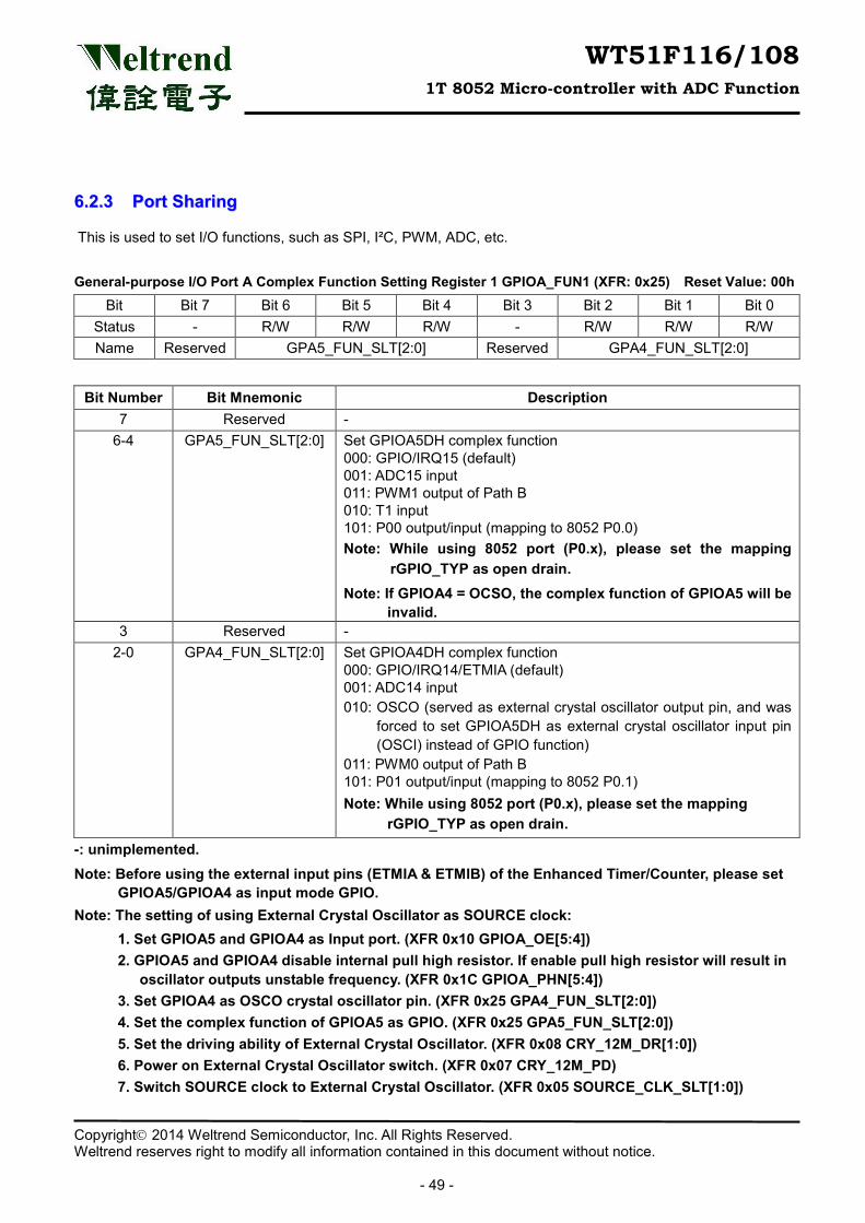
WT51F116/108 1T 8052 Micro-controller with ADC Function
Copyright 2014 Weltrend Semiconductor, Inc. All Rights Reserved. Weltrend reserves right to modify all information contained in this document without notice.
- 49 -
66..22..33 PPoorrtt SShhaarriinngg
This is used to set I/O functions, such as SPI, I²C, PWM, ADC, etc. General-purpose I/O Port A Complex Function Setting Register 1 GPIOA_FUN1 (XFR: 0x25) Reset Value: 00h
Bit Bit 7 Bit 6 Bit 5 Bit 4 Bit 3 Bit 2 Bit 1 Bit 0 Status - R/W R/W R/W - R/W R/W R/W Name Reserved GPA5_FUN_SLT[2:0] Reserved GPA4_FUN_SLT[2:0]
Bit Number Bit Mnemonic Description 7 Reserved -
6-4 GPA5_FUN_SLT[2:0] Set GPIOA5DH complex function 000: GPIO/IRQ15 (default) 001: ADC15 input 011: PWM1 output of Path B 010: T1 input 101: P00 output/input (mapping to 8052 P0.0) Note: While using 8052 port (P0.x), please set the mapping
rGPIO_TYP as open drain. Note: If GPIOA4 = OCSO, the complex function of GPIOA5 will be
invalid. 3 Reserved -
2-0 GPA4_FUN_SLT[2:0] Set GPIOA4DH complex function 000: GPIO/IRQ14/ETMIA (default) 001: ADC14 input 010: OSCO (served as external crystal oscillator output pin, and was
forced to set GPIOA5DH as external crystal oscillator input pin (OSCI) instead of GPIO function)
011: PWM0 output of Path B 101: P01 output/input (mapping to 8052 P0.1) Note: While using 8052 port (P0.x), please set the mapping
rGPIO_TYP as open drain.
-: unimplemented.
Note: Before using the external input pins (ETMIA & ETMIB) of the Enhanced Timer/Counter, please set GPIOA5/GPIOA4 as input mode GPIO.
Note: The setting of using External Crystal Oscillator as SOURCE clock: 1. Set GPIOA5 and GPIOA4 as Input port. (XFR 0x10 GPIOA_OE[5:4]) 2. GPIOA5 and GPIOA4 disable internal pull high resistor. If enable pull high resistor will result in
oscillator outputs unstable frequency. (XFR 0x1C GPIOA_PHN[5:4]) 3. Set GPIOA4 as OSCO crystal oscillator pin. (XFR 0x25 GPA4_FUN_SLT[2:0]) 4. Set the complex function of GPIOA5 as GPIO. (XFR 0x25 GPA5_FUN_SLT[2:0]) 5. Set the driving ability of External Crystal Oscillator. (XFR 0x08 CRY_12M_DR[1:0]) 6. Power on External Crystal Oscillator switch. (XFR 0x07 CRY_12M_PD) 7. Switch SOURCE clock to External Crystal Oscillator. (XFR 0x05 SOURCE_CLK_SLT[1:0])
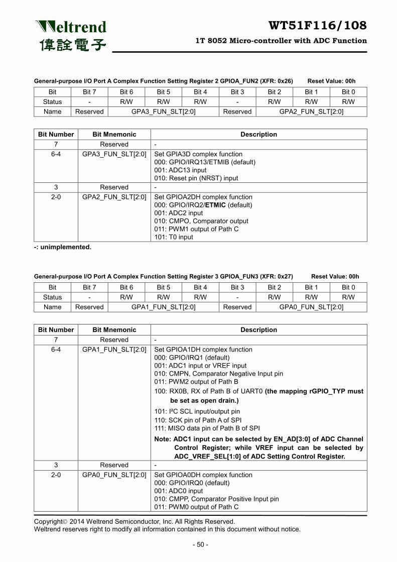
WT51F116/108 1T 8052 Micro-controller with ADC Function
Copyright 2014 Weltrend Semiconductor, Inc. All Rights Reserved. Weltrend reserves right to modify all information contained in this document without notice.
- 50 -
General-purpose I/O Port A Complex Function Setting Register 2 GPIOA_FUN2 (XFR: 0x26) Reset Value: 00h
Bit Bit 7 Bit 6 Bit 5 Bit 4 Bit 3 Bit 2 Bit 1 Bit 0 Status - R/W R/W R/W - R/W R/W R/W Name Reserved GPA3_FUN_SLT[2:0] Reserved GPA2_FUN_SLT[2:0]
Bit Number Bit Mnemonic Description 7 Reserved -
6-4 GPA3_FUN_SLT[2:0] Set GPIA3D complex function 000: GPIO/IRQ13/ETMIB (default) 001: ADC13 input 010: Reset pin (NRST) input
3 Reserved - 2-0 GPA2_FUN_SLT[2:0] Set GPIOA2DH complex function
000: GPIO/IRQ2/ETMIC (default) 001: ADC2 input 010: CMPO, Comparator output 011: PWM1 output of Path C 101: T0 input
-: unimplemented.
General-purpose I/O Port A Complex Function Setting Register 3 GPIOA_FUN3 (XFR: 0x27) Reset Value: 00h
Bit Bit 7 Bit 6 Bit 5 Bit 4 Bit 3 Bit 2 Bit 1 Bit 0 Status - R/W R/W R/W - R/W R/W R/W Name Reserved GPA1_FUN_SLT[2:0] Reserved GPA0_FUN_SLT[2:0]
Bit Number Bit Mnemonic Description 7 Reserved -
6-4 GPA1_FUN_SLT[2:0] Set GPIOA1DH complex function 000: GPIO/IRQ1 (default) 001: ADC1 input or VREF input 010: CMPN, Comparator Negative Input pin 011: PWM2 output of Path B 100: RX0B, RX of Path B of UART0 (the mapping rGPIO_TYP must
be set as open drain.) 101: I²C SCL input/output pin 110: SCK pin of Path A of SPI 111: MISO data pin of Path B of SPI Note: ADC1 input can be selected by EN_AD[3:0] of ADC Channel
Control Register; while VREF input can be selected by ADC_VREF_SEL[1:0] of ADC Setting Control Register.
3 Reserved - 2-0 GPA0_FUN_SLT[2:0] Set GPIOA0DH complex function
000: GPIO/IRQ0 (default) 001: ADC0 input 010: CMPP, Comparator Positive Input pin 011: PWM0 output of Path C
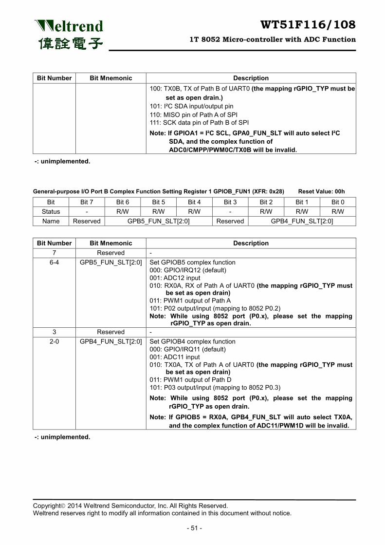
WT51F116/108 1T 8052 Micro-controller with ADC Function
Copyright 2014 Weltrend Semiconductor, Inc. All Rights Reserved. Weltrend reserves right to modify all information contained in this document without notice.
- 51 -
Bit Number Bit Mnemonic Description 100: TX0B, TX of Path B of UART0 (the mapping rGPIO_TYP must be
set as open drain.) 101: I²C SDA input/output pin 110: MISO pin of Path A of SPI 111: SCK data pin of Path B of SPI Note: If GPIOA1 = I²C SCL, GPA0_FUN_SLT will auto select I²C
SDA, and the complex function of ADC0/CMPP/PWM0C/TX0B will be invalid.
-: unimplemented.
General-purpose I/O Port B Complex Function Setting Register 1 GPIOB_FUN1 (XFR: 0x28) Reset Value: 00h
Bit Bit 7 Bit 6 Bit 5 Bit 4 Bit 3 Bit 2 Bit 1 Bit 0 Status - R/W R/W R/W - R/W R/W R/W Name Reserved GPB5_FUN_SLT[2:0] Reserved GPB4_FUN_SLT[2:0]
Bit Number Bit Mnemonic Description 7 Reserved -
6-4 GPB5_FUN_SLT[2:0] Set GPIOB5 complex function 000: GPIO/IRQ12 (default) 001: ADC12 input 010: RX0A, RX of Path A of UART0 (the mapping rGPIO_TYP must
be set as open drain) 011: PWM1 output of Path A 101: P02 output/input (mapping to 8052 P0.2) Note: While using 8052 port (P0.x), please set the mapping
rGPIO_TYP as open drain. 3 Reserved -
2-0 GPB4_FUN_SLT[2:0] Set GPIOB4 complex function 000: GPIO/IRQ11 (default) 001: ADC11 input 010: TX0A, TX of Path A of UART0 (the mapping rGPIO_TYP must
be set as open drain) 011: PWM1 output of Path D 101: P03 output/input (mapping to 8052 P0.3) Note: While using 8052 port (P0.x), please set the mapping
rGPIO_TYP as open drain. Note: If GPIOB5 = RX0A, GPB4_FUN_SLT will auto select TX0A,
and the complex function of ADC11/PWM1D will be invalid.
-: unimplemented.
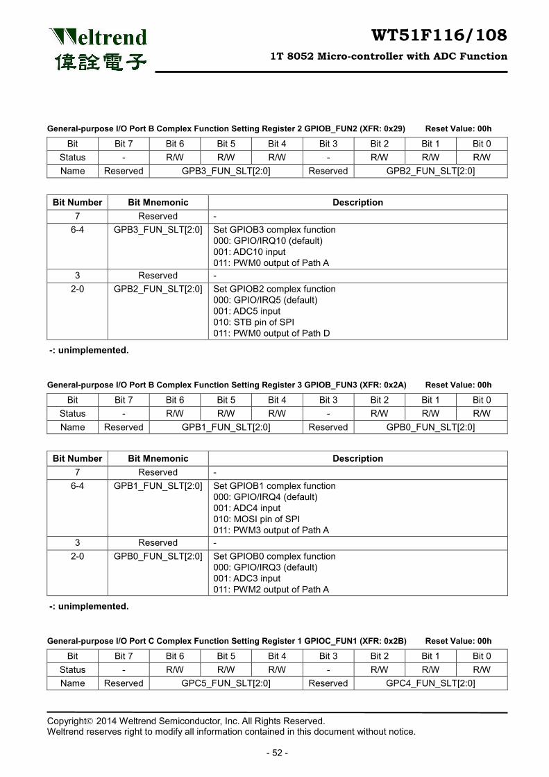
WT51F116/108 1T 8052 Micro-controller with ADC Function
Copyright 2014 Weltrend Semiconductor, Inc. All Rights Reserved. Weltrend reserves right to modify all information contained in this document without notice.
- 52 -
General-purpose I/O Port B Complex Function Setting Register 2 GPIOB_FUN2 (XFR: 0x29) Reset Value: 00h
Bit Bit 7 Bit 6 Bit 5 Bit 4 Bit 3 Bit 2 Bit 1 Bit 0 Status - R/W R/W R/W - R/W R/W R/W Name Reserved GPB3_FUN_SLT[2:0] Reserved GPB2_FUN_SLT[2:0]
Bit Number Bit Mnemonic Description 7 Reserved -
6-4 GPB3_FUN_SLT[2:0] Set GPIOB3 complex function 000: GPIO/IRQ10 (default) 001: ADC10 input 011: PWM0 output of Path A
3 Reserved - 2-0 GPB2_FUN_SLT[2:0] Set GPIOB2 complex function
000: GPIO/IRQ5 (default) 001: ADC5 input 010: STB pin of SPI 011: PWM0 output of Path D
-: unimplemented.
General-purpose I/O Port B Complex Function Setting Register 3 GPIOB_FUN3 (XFR: 0x2A) Reset Value: 00h
Bit Bit 7 Bit 6 Bit 5 Bit 4 Bit 3 Bit 2 Bit 1 Bit 0 Status - R/W R/W R/W - R/W R/W R/W Name Reserved GPB1_FUN_SLT[2:0] Reserved GPB0_FUN_SLT[2:0]
Bit Number Bit Mnemonic Description 7 Reserved -
6-4 GPB1_FUN_SLT[2:0] Set GPIOB1 complex function 000: GPIO/IRQ4 (default) 001: ADC4 input 010: MOSI pin of SPI 011: PWM3 output of Path A
3 Reserved - 2-0 GPB0_FUN_SLT[2:0] Set GPIOB0 complex function
000: GPIO/IRQ3 (default) 001: ADC3 input 011: PWM2 output of Path A
-: unimplemented.
General-purpose I/O Port C Complex Function Setting Register 1 GPIOC_FUN1 (XFR: 0x2B) Reset Value: 00h
Bit Bit 7 Bit 6 Bit 5 Bit 4 Bit 3 Bit 2 Bit 1 Bit 0 Status - R/W R/W R/W - R/W R/W R/W Name Reserved GPC5_FUN_SLT[2:0] Reserved GPC4_FUN_SLT[2:0]
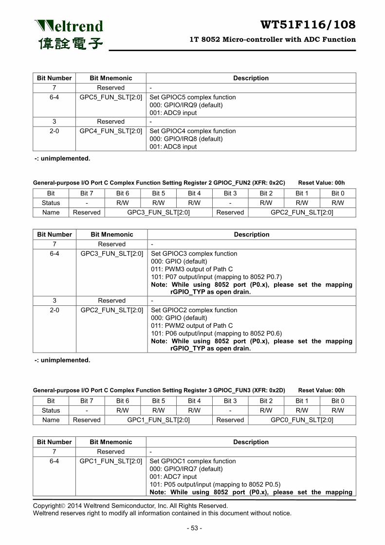
WT51F116/108 1T 8052 Micro-controller with ADC Function
Copyright 2014 Weltrend Semiconductor, Inc. All Rights Reserved. Weltrend reserves right to modify all information contained in this document without notice.
- 53 -
Bit Number Bit Mnemonic Description 7 Reserved -
6-4 GPC5_FUN_SLT[2:0] Set GPIOC5 complex function 000: GPIO/IRQ9 (default) 001: ADC9 input
3 Reserved - 2-0 GPC4_FUN_SLT[2:0] Set GPIOC4 complex function
000: GPIO/IRQ8 (default) 001: ADC8 input
-: unimplemented.
General-purpose I/O Port C Complex Function Setting Register 2 GPIOC_FUN2 (XFR: 0x2C) Reset Value: 00h
Bit Bit 7 Bit 6 Bit 5 Bit 4 Bit 3 Bit 2 Bit 1 Bit 0 Status - R/W R/W R/W - R/W R/W R/W Name Reserved GPC3_FUN_SLT[2:0] Reserved GPC2_FUN_SLT[2:0]
Bit Number Bit Mnemonic Description 7 Reserved -
6-4 GPC3_FUN_SLT[2:0] Set GPIOC3 complex function 000: GPIO (default) 011: PWM3 output of Path C 101: P07 output/input (mapping to 8052 P0.7) Note: While using 8052 port (P0.x), please set the mapping
rGPIO_TYP as open drain. 3 Reserved -
2-0 GPC2_FUN_SLT[2:0] Set GPIOC2 complex function 000: GPIO (default) 011: PWM2 output of Path C 101: P06 output/input (mapping to 8052 P0.6) Note: While using 8052 port (P0.x), please set the mapping
rGPIO_TYP as open drain.
-: unimplemented.
General-purpose I/O Port C Complex Function Setting Register 3 GPIOC_FUN3 (XFR: 0x2D) Reset Value: 00h
Bit Bit 7 Bit 6 Bit 5 Bit 4 Bit 3 Bit 2 Bit 1 Bit 0 Status - R/W R/W R/W - R/W R/W R/W Name Reserved GPC1_FUN_SLT[2:0] Reserved GPC0_FUN_SLT[2:0]
Bit Number Bit Mnemonic Description 7 Reserved -
6-4 GPC1_FUN_SLT[2:0] Set GPIOC1 complex function 000: GPIO/IRQ7 (default) 001: ADC7 input 101: P05 output/input (mapping to 8052 P0.5) Note: While using 8052 port (P0.x), please set the mapping
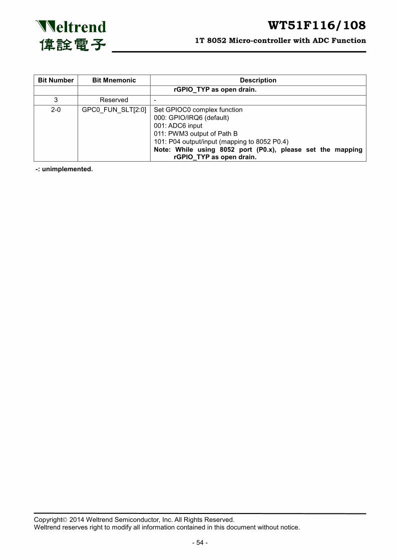
WT51F116/108 1T 8052 Micro-controller with ADC Function
Copyright 2014 Weltrend Semiconductor, Inc. All Rights Reserved. Weltrend reserves right to modify all information contained in this document without notice.
- 54 -
Bit Number Bit Mnemonic Description rGPIO_TYP as open drain.
3 Reserved - 2-0 GPC0_FUN_SLT[2:0] Set GPIOC0 complex function
000: GPIO/IRQ6 (default) 001: ADC6 input 011: PWM3 output of Path B 101: P04 output/input (mapping to 8052 P0.4) Note: While using 8052 port (P0.x), please set the mapping
rGPIO_TYP as open drain.
-: unimplemented.
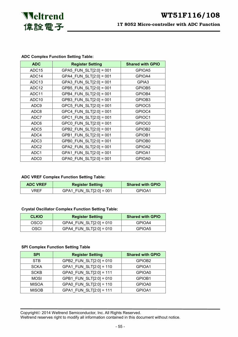
WT51F116/108 1T 8052 Micro-controller with ADC Function
Copyright 2014 Weltrend Semiconductor, Inc. All Rights Reserved. Weltrend reserves right to modify all information contained in this document without notice.
- 55 -
ADC Complex Function Setting Table:
ADC Register Setting Shared with GPIO ADC15 GPA5_FUN_SLT[2:0] = 001 GPIOA5 ADC14 GPA4_FUN_SLT[2:0] = 001 GPIOA4 ADC13 GPA3_FUN_SLT[2:0] = 001 GPIA3 ADC12 GPB5_FUN_SLT[2:0] = 001 GPIOB5 ADC11 GPB4_FUN_SLT[2:0] = 001 GPIOB4 ADC10 GPB3_FUN_SLT[2:0] = 001 GPIOB3 ADC9 GPC5_FUN_SLT[2:0] = 001 GPIOC5 ADC8 GPC4_FUN_SLT[2:0] = 001 GPIOC4 ADC7 GPC1_FUN_SLT[2:0] = 001 GPIOC1 ADC6 GPC0_FUN_SLT[2:0] = 001 GPIOC0 ADC5 GPB2_FUN_SLT[2:0] = 001 GPIOB2 ADC4 GPB1_FUN_SLT[2:0] = 001 GPIOB1 ADC3 GPB0_FUN_SLT[2:0] = 001 GPIOB0 ADC2 GPA2_FUN_SLT[2:0] = 001 GPIOA2 ADC1 GPA1_FUN_SLT[2:0] = 001 GPIOA1 ADC0 GPA0_FUN_SLT[2:0] = 001 GPIOA0
ADC VREF Complex Function Setting Table:
ADC VREF Register Setting Shared with GPIO VREF GPA1_FUN_SLT[2:0] = 001 GPIOA1
Crystal Oscillator Complex Function Setting Table:
CLKIO Register Setting Shared with GPIO OSCO GPA4_FUN_SLT[2:0] = 010 GPIOA4 OSCI GPA4_FUN_SLT[2:0] = 010 GPIOA5
SPI Complex Function Setting Table
SPI Register Setting Shared with GPIO STB GPB2_FUN_SLT[2:0] = 010 GPIOB2
SCKA GPA1_FUN_SLT[2:0] = 110 GPIOA1 SCKB GPA0_FUN_SLT[2:0] = 111 GPIOA0 MOSI GPB1_FUN_SLT[2:0] = 010 GPIOB1
MISOA GPA0_FUN_SLT[2:0] = 110 GPIOA0 MISOB GPA1_FUN_SLT[2:0] = 111 GPIOA1
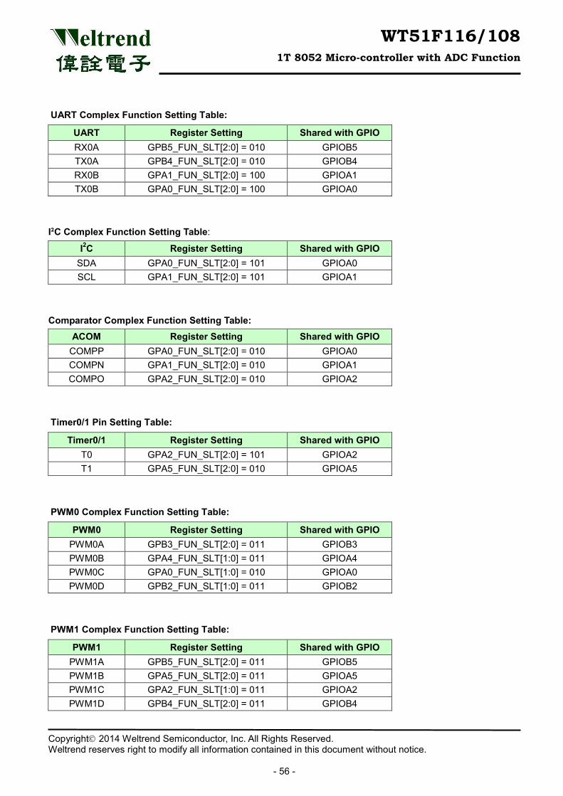
WT51F116/108 1T 8052 Micro-controller with ADC Function
Copyright 2014 Weltrend Semiconductor, Inc. All Rights Reserved. Weltrend reserves right to modify all information contained in this document without notice.
- 56 -
UART Complex Function Setting Table:
UART Register Setting Shared with GPIO RX0A GPB5_FUN_SLT[2:0] = 010 GPIOB5 TX0A GPB4_FUN_SLT[2:0] = 010 GPIOB4 RX0B GPA1_FUN_SLT[2:0] = 100 GPIOA1 TX0B GPA0_FUN_SLT[2:0] = 100 GPIOA0
I²C Complex Function Setting Table:
I2C Register Setting Shared with GPIO SDA GPA0_FUN_SLT[2:0] = 101 GPIOA0 SCL GPA1_FUN_SLT[2:0] = 101 GPIOA1
Comparator Complex Function Setting Table: ACOM Register Setting Shared with GPIO
COMPP GPA0_FUN_SLT[2:0] = 010 GPIOA0 COMPN GPA1_FUN_SLT[2:0] = 010 GPIOA1 COMPO GPA2_FUN_SLT[2:0] = 010 GPIOA2
Timer0/1 Pin Setting Table:
Timer0/1 Register Setting Shared with GPIO T0 GPA2_FUN_SLT[2:0] = 101 GPIOA2 T1 GPA5_FUN_SLT[2:0] = 010 GPIOA5
PWM0 Complex Function Setting Table:
PWM0 Register Setting Shared with GPIO PWM0A GPB3_FUN_SLT[2:0] = 011 GPIOB3 PWM0B GPA4_FUN_SLT[1:0] = 011 GPIOA4 PWM0C GPA0_FUN_SLT[1:0] = 010 GPIOA0 PWM0D GPB2_FUN_SLT[1:0] = 011 GPIOB2
PWM1 Complex Function Setting Table:
PWM1 Register Setting Shared with GPIO PWM1A GPB5_FUN_SLT[2:0] = 011 GPIOB5 PWM1B GPA5_FUN_SLT[2:0] = 011 GPIOA5 PWM1C GPA2_FUN_SLT[1:0] = 011 GPIOA2 PWM1D GPB4_FUN_SLT[2:0] = 011 GPIOB4
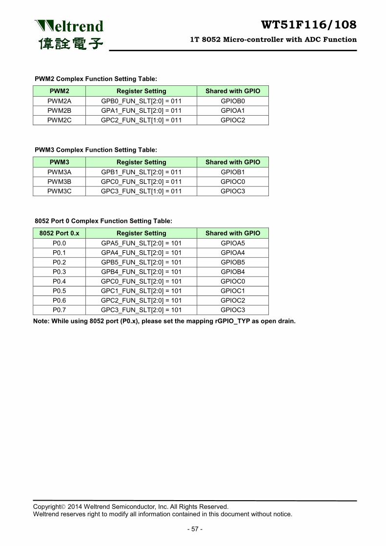
WT51F116/108 1T 8052 Micro-controller with ADC Function
Copyright 2014 Weltrend Semiconductor, Inc. All Rights Reserved. Weltrend reserves right to modify all information contained in this document without notice.
- 57 -
PWM2 Complex Function Setting Table:
PWM2 Register Setting Shared with GPIO PWM2A GPB0_FUN_SLT[2:0] = 011 GPIOB0 PWM2B GPA1_FUN_SLT[2:0] = 011 GPIOA1 PWM2C GPC2_FUN_SLT[1:0] = 011 GPIOC2
PWM3 Complex Function Setting Table:
PWM3 Register Setting Shared with GPIO PWM3A GPB1_FUN_SLT[2:0] = 011 GPIOB1 PWM3B GPC0_FUN_SLT[2:0] = 011 GPIOC0 PWM3C GPC3_FUN_SLT[1:0] = 011 GPIOC3
8052 Port 0 Complex Function Setting Table:
8052 Port 0.x Register Setting Shared with GPIO P0.0 GPA5_FUN_SLT[2:0] = 101 GPIOA5 P0.1 GPA4_FUN_SLT[2:0] = 101 GPIOA4 P0.2 GPB5_FUN_SLT[2:0] = 101 GPIOB5 P0.3 GPB4_FUN_SLT[2:0] = 101 GPIOB4 P0.4 GPC0_FUN_SLT[2:0] = 101 GPIOC0 P0.5 GPC1_FUN_SLT[2:0] = 101 GPIOC1 P0.6 GPC2_FUN_SLT[2:0] = 101 GPIOC2 P0.7 GPC3_FUN_SLT[2:0] = 101 GPIOC3
Note: While using 8052 port (P0.x), please set the mapping rGPIO_TYP as open drain.
WT51F116/108 1T 8052 Micro-controller with ADC Function
Copyright 2014 Weltrend Semiconductor, Inc. All Rights Reserved. Weltrend reserves right to modify all information contained in this document without notice.
- 58 -
66..33 IInntteerrrruupptt The WT51F116/108 provides eight 8052 Interrupt sources: four 8052 External Interrupts (INT0, INT1, INT2, INT3), three Timer/Counter Interrupts (TF0, TF1, TF2), and one UART Interrupt (RI0/TI0). Each of these interrupt sources has its own enable control bit, and can be individually enabled or disabled by setting or clearing the corresponding bit in the Special Function Register IE0 or XICON. When an interrupt is generated, CPU will jump to interrupt vector from service routine as listed below. If multiple requests of different priority levels are received simultaneously, the request of higher priority level is serviced, and then returned to service routine through RETI instruction. If interrupt flag bit is set, CPU will enter the Interrupt processing again.
Interrupt Vector Table of 8052 & Priority Level Structure:
Keil C Interrupt Number Interrupt sources Vector
Address Priority Level
(default) Interrupt Enable
Register 0 8052 external interrupt 0 03H 1 IE.0 (EX0) 1 Timer/Counter 0 interrupt 0BH 2 IE.1 (ET0) 2 8052 external interrupt 1 13H 3 IE.2 (EX1) 3 Timer/Counter 1 interrupt 1BH 4 IE.3 (ET1) 4 Serial port 0 interrupt (UART0) 23H 5 IE.4 (ES) 5 Timer/Counter 2 interrupt 2BH 6 IE.5 (ET2) 7 8052 external interrupt 2 3BH 7 XICON.2 (EX2) 8 8052 external interrupt 3 43H 8 XICON.6 (EX3)
Interrupt Enable Register 0
IE (8052 interrupt enable register, including INT0/INT1) Address: A8H Reset Value: 00h
7 6 5 4 3 2 1 0 EA ES1 ET2 ES ET1 EX1 ET0 EX0
Bit Number Bit Mnemonic Description 7 EA 1: Enable all interrupt function
0: Disable all interrupt function 6 ES1 1: Enable UART 1 interrupt (function not available in
WT51F116/108 & WT51F104) 0: Disable UART 1 interrupt
5 ET2 1: Enable Timer/Counter 2 interrupt (function not available in WT51F104)
0: Disable Timer/Counter 2 interrupt 4 ES 1: Enable UART 0 interrupt
0: Disable UART 0 interrupt
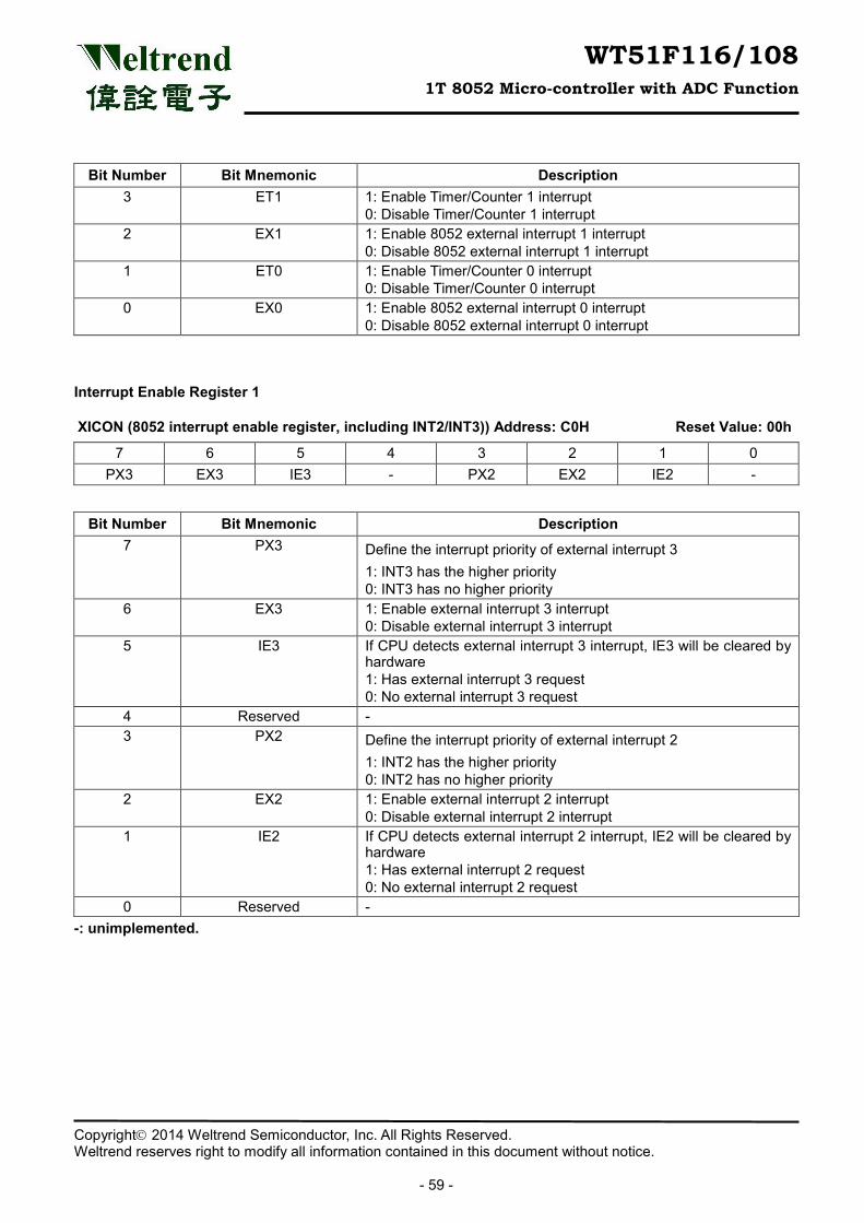
WT51F116/108 1T 8052 Micro-controller with ADC Function
Copyright 2014 Weltrend Semiconductor, Inc. All Rights Reserved. Weltrend reserves right to modify all information contained in this document without notice.
- 59 -
Bit Number Bit Mnemonic Description 3 ET1 1: Enable Timer/Counter 1 interrupt
0: Disable Timer/Counter 1 interrupt 2 EX1 1: Enable 8052 external interrupt 1 interrupt
0: Disable 8052 external interrupt 1 interrupt 1 ET0 1: Enable Timer/Counter 0 interrupt
0: Disable Timer/Counter 0 interrupt 0 EX0 1: Enable 8052 external interrupt 0 interrupt
0: Disable 8052 external interrupt 0 interrupt
Interrupt Enable Register 1
XICON (8052 interrupt enable register, including INT2/INT3)) Address: C0H Reset Value: 00h
7 6 5 4 3 2 1 0 PX3 EX3 IE3 - PX2 EX2 IE2 -
Bit Number Bit Mnemonic Description 7 PX3 Define the interrupt priority of external interrupt 3
1: INT3 has the higher priority 0: INT3 has no higher priority
6 EX3 1: Enable external interrupt 3 interrupt 0: Disable external interrupt 3 interrupt
5 IE3 If CPU detects external interrupt 3 interrupt, IE3 will be cleared by hardware 1: Has external interrupt 3 request 0: No external interrupt 3 request
4 Reserved - 3 PX2 Define the interrupt priority of external interrupt 2
1: INT2 has the higher priority 0: INT2 has no higher priority
2 EX2 1: Enable external interrupt 2 interrupt 0: Disable external interrupt 2 interrupt
1 IE2 If CPU detects external interrupt 2 interrupt, IE2 will be cleared by hardware 1: Has external interrupt 2 request 0: No external interrupt 2 request
0 Reserved - -: unimplemented.
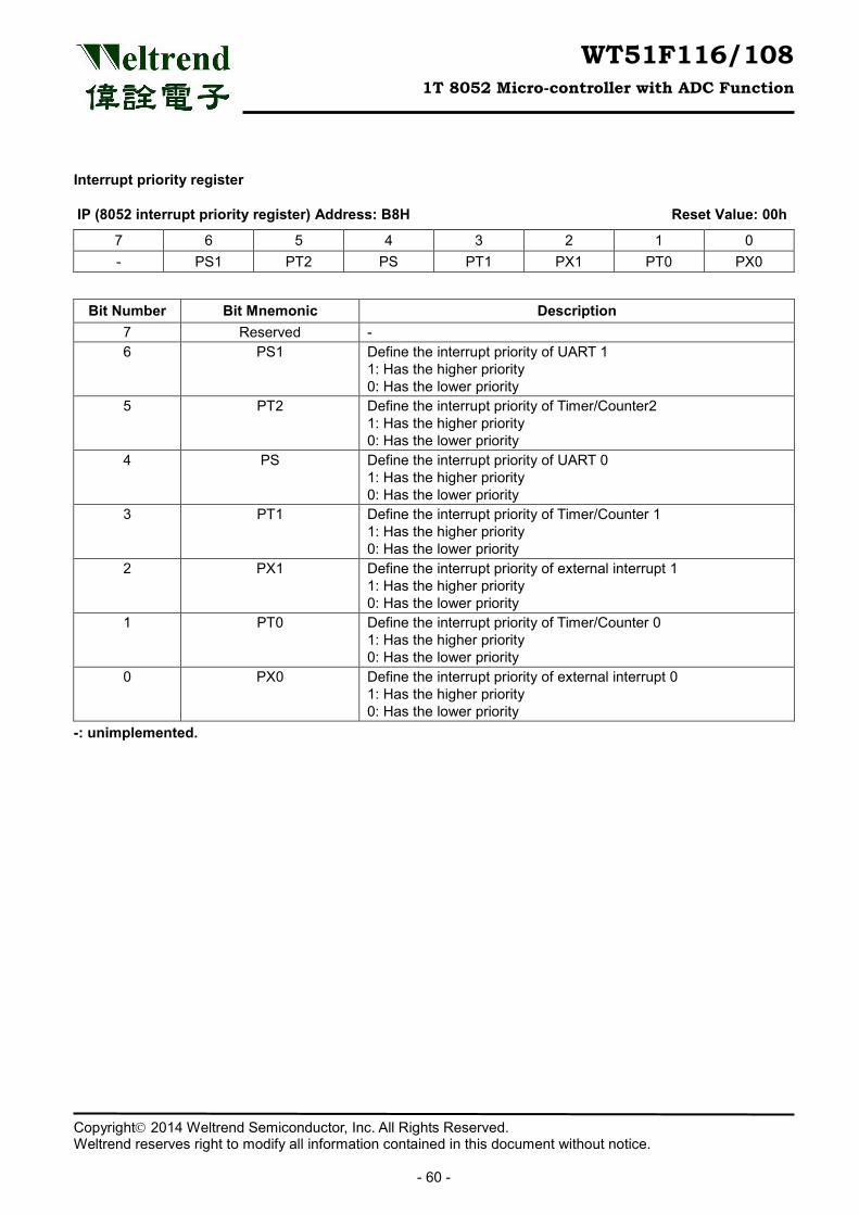
WT51F116/108 1T 8052 Micro-controller with ADC Function
Copyright 2014 Weltrend Semiconductor, Inc. All Rights Reserved. Weltrend reserves right to modify all information contained in this document without notice.
- 60 -
Interrupt priority register
IP (8052 interrupt priority register) Address: B8H Reset Value: 00h
7 6 5 4 3 2 1 0 - PS1 PT2 PS PT1 PX1 PT0 PX0
Bit Number Bit Mnemonic Description 7 Reserved - 6 PS1 Define the interrupt priority of UART 1
1: Has the higher priority 0: Has the lower priority
5 PT2 Define the interrupt priority of Timer/Counter2 1: Has the higher priority 0: Has the lower priority
4 PS Define the interrupt priority of UART 0 1: Has the higher priority 0: Has the lower priority
3 PT1 Define the interrupt priority of Timer/Counter 1 1: Has the higher priority 0: Has the lower priority
2 PX1 Define the interrupt priority of external interrupt 1 1: Has the higher priority 0: Has the lower priority
1 PT0 Define the interrupt priority of Timer/Counter 0 1: Has the higher priority 0: Has the lower priority
0 PX0 Define the interrupt priority of external interrupt 0 1: Has the higher priority 0: Has the lower priority
-: unimplemented.
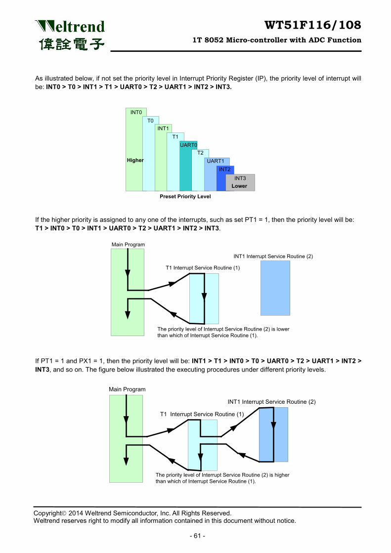
WT51F116/108 1T 8052 Micro-controller with ADC Function
Copyright 2014 Weltrend Semiconductor, Inc. All Rights Reserved. Weltrend reserves right to modify all information contained in this document without notice.
- 61 -
As illustrated below, if not set the priority level in Interrupt Priority Register (IP), the priority level of interrupt will be: INT0 > T0 > INT1 > T1 > UART0 > T2 > UART1 > INT2 > INT3.
INT0
UART1
INT1
INT2
INT3
T2UART0
T1
T0
Preset Priority Level
Lower
Higher
If the higher priority is assigned to any one of the interrupts, such as set PT1 = 1, then the priority level will be: T1 > INT0 > T0 > INT1 > UART0 > T2 > UART1 > INT2 > INT3.
Main Program
T1 Interrupt Service Routine (1)
The priority level of Interrupt Service Routine (2) is lower than which of Interrupt Service Routine (1).
INT1 Interrupt Service Routine (2)
If PT1 = 1 and PX1 = 1, then the priority level will be: INT1 > T1 > INT0 > T0 > UART0 > T2 > UART1 > INT2 > INT3, and so on. The figure below illustrated the executing procedures under different priority levels.
Main Program
T1 Interrupt Service Routine (1)
INT1 Interrupt Service Routine (2)
The priority level of Interrupt Service Routine (2) is higherthan which of Interrupt Service Routine (1).
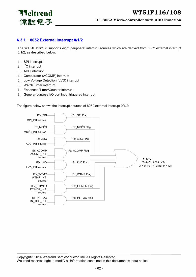
WT51F116/108 1T 8052 Micro-controller with ADC Function
Copyright 2014 Weltrend Semiconductor, Inc. All Rights Reserved. Weltrend reserves right to modify all information contained in this document without notice.
- 62 -
66..33..11 88005522 EExxtteerrnnaall IInntteerrrruupptt 00//11//22
The WT51F116/108 supports eight peripheral interrupt sources which are derived from 8052 external interrupt 0/1/2, as described below. 1. SPI interrupt 2. I2C interrupt 3. ADC interrupt 4. Comparator (ACOMP) interrupt 5. Low Voltage Detection (LVD) interrupt 6. Watch Timer interrupt 7. Enhanced Timer/Counter interrupt 8. General-purpose I/O port input triggered interrupt
The figure below shows the interrupt sources of 8052 external interrupt 0/1/2:
IEx_SPI IFx_SPI Flag
IEx_MSI2C IFx_MSI2C Flag
IEx_ADC IFx_ADC Flag
IEx_ACOMP IFx_ACOMP Flag
IEx_LVD IFx_LVD Flag
IEx_WTMR IFx_WTMR Flag
IEx_ETIMER IFx_ETIMER Flag
IEx_IN_TOG IFx_IN_TOG Flag
INTxTo MCU 8052 INTx
X = 0/1/2 (INT0/INT1/INT2)
IN_TOG_INT source
ETIMER_INT source
WTMR_INT source
LVD_INT source
ACOMP_INT source
ADC_INT source
MSI2C_INT source
SPI_INT source
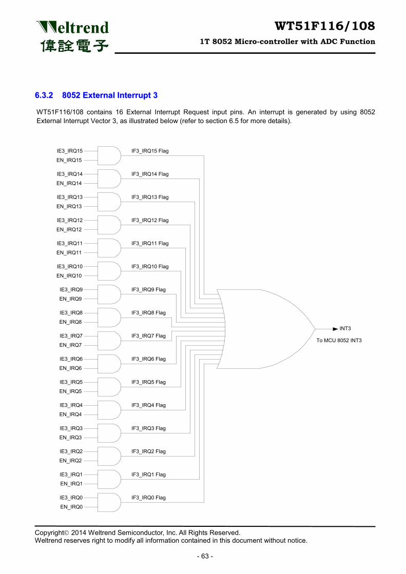
WT51F116/108 1T 8052 Micro-controller with ADC Function
Copyright 2014 Weltrend Semiconductor, Inc. All Rights Reserved. Weltrend reserves right to modify all information contained in this document without notice.
- 63 -
66..33..22 88005522 EExxtteerrnnaall IInntteerrrruupptt 33
WT51F116/108 contains 16 External Interrupt Request input pins. An interrupt is generated by using 8052 External Interrupt Vector 3, as illustrated below (refer to section 6.5 for more details).
IE3_IRQ15 IF3_IRQ15 Flag
IE3_IRQ14 IF3_IRQ14 Flag
IE3_IRQ13 IF3_IRQ13 Flag
IE3_IRQ12 IF3_IRQ12 Flag
IE3_IRQ11 IF3_IRQ11 Flag
IE3_IRQ10 IF3_IRQ10 Flag
IE3_IRQ9 IF3_IRQ9 Flag
IE3_IRQ8 IF3_IRQ8 Flag
INT3
To MCU 8052 INT3
EN_IRQ15
EN_IRQ14
EN_IRQ13
EN_IRQ12
EN_IRQ8
EN_IRQ9
EN_IRQ10
EN_IRQ11
IE3_IRQ7 IF3_IRQ7 Flag
IE3_IRQ6 IF3_IRQ6 Flag
IE3_IRQ5 IF3_IRQ5 Flag
IE3_IRQ4 IF3_IRQ4 Flag
IE3_IRQ3 IF3_IRQ3 Flag
IE3_IRQ2 IF3_IRQ2 Flag
IE3_IRQ1 IF3_IRQ1 Flag
IE3_IRQ0 IF3_IRQ0 Flag
EN_IRQ7
EN_IRQ6
EN_IRQ5
EN_IRQ4
EN_IRQ0
EN_IRQ1
EN_IRQ2
EN_IRQ3
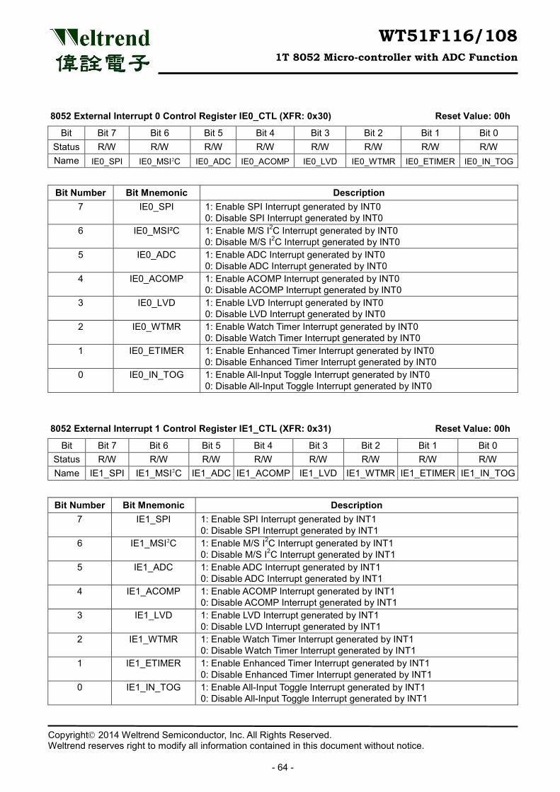
WT51F116/108 1T 8052 Micro-controller with ADC Function
Copyright 2014 Weltrend Semiconductor, Inc. All Rights Reserved. Weltrend reserves right to modify all information contained in this document without notice.
- 64 -
8052 External Interrupt 0 Control Register IE0_CTL (XFR: 0x30) Reset Value: 00h
Bit Bit 7 Bit 6 Bit 5 Bit 4 Bit 3 Bit 2 Bit 1 Bit 0 Status R/W R/W R/W R/W R/W R/W R/W R/W Name IE0_SPI IE0_MSI²C IE0_ADC IE0_ACOMP IE0_LVD IE0_WTMR IE0_ETIMER IE0_IN_TOG
Bit Number Bit Mnemonic Description 7 IE0_SPI 1: Enable SPI Interrupt generated by INT0
0: Disable SPI Interrupt generated by INT0 6 IE0_MSI²C 1: Enable M/S I2C Interrupt generated by INT0
0: Disable M/S I2C Interrupt generated by INT0 5 IE0_ADC 1: Enable ADC Interrupt generated by INT0
0: Disable ADC Interrupt generated by INT0 4 IE0_ACOMP 1: Enable ACOMP Interrupt generated by INT0
0: Disable ACOMP Interrupt generated by INT0 3 IE0_LVD 1: Enable LVD Interrupt generated by INT0
0: Disable LVD Interrupt generated by INT0 2 IE0_WTMR 1: Enable Watch Timer Interrupt generated by INT0
0: Disable Watch Timer Interrupt generated by INT0 1 IE0_ETIMER 1: Enable Enhanced Timer Interrupt generated by INT0
0: Disable Enhanced Timer Interrupt generated by INT0 0 IE0_IN_TOG 1: Enable All-Input Toggle Interrupt generated by INT0
0: Disable All-Input Toggle Interrupt generated by INT0
8052 External Interrupt 1 Control Register IE1_CTL (XFR: 0x31) Reset Value: 00h
Bit Bit 7 Bit 6 Bit 5 Bit 4 Bit 3 Bit 2 Bit 1 Bit 0 Status R/W R/W R/W R/W R/W R/W R/W R/W Name IE1_SPI IE1_MSI²C IE1_ADC IE1_ACOMP IE1_LVD IE1_WTMR IE1_ETIMER IE1_IN_TOG
Bit Number Bit Mnemonic Description 7 IE1_SPI 1: Enable SPI Interrupt generated by INT1
0: Disable SPI Interrupt generated by INT1 6 IE1_MSI²C 1: Enable M/S I2C Interrupt generated by INT1
0: Disable M/S I2C Interrupt generated by INT1 5 IE1_ADC 1: Enable ADC Interrupt generated by INT1
0: Disable ADC Interrupt generated by INT1 4 IE1_ACOMP 1: Enable ACOMP Interrupt generated by INT1
0: Disable ACOMP Interrupt generated by INT1 3 IE1_LVD 1: Enable LVD Interrupt generated by INT1
0: Disable LVD Interrupt generated by INT1 2 IE1_WTMR 1: Enable Watch Timer Interrupt generated by INT1
0: Disable Watch Timer Interrupt generated by INT1 1 IE1_ETIMER 1: Enable Enhanced Timer Interrupt generated by INT1
0: Disable Enhanced Timer Interrupt generated by INT1 0 IE1_IN_TOG 1: Enable All-Input Toggle Interrupt generated by INT1
0: Disable All-Input Toggle Interrupt generated by INT1
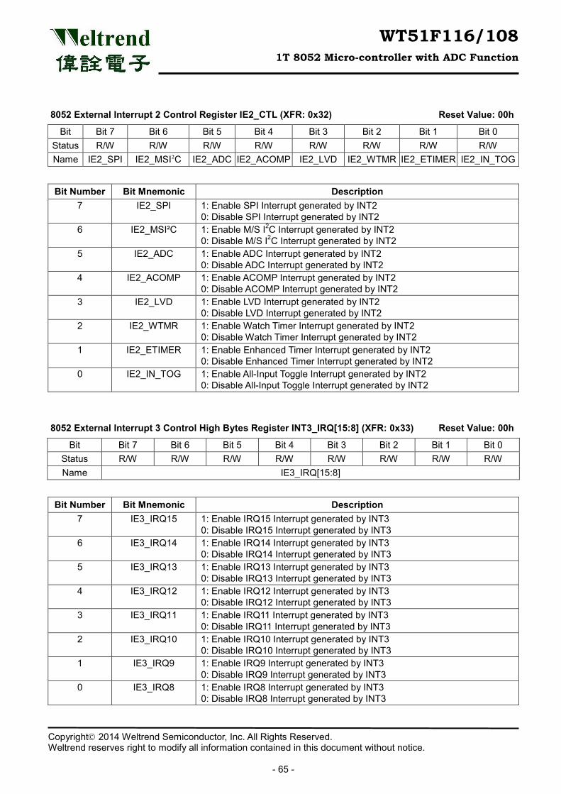
WT51F116/108 1T 8052 Micro-controller with ADC Function
Copyright 2014 Weltrend Semiconductor, Inc. All Rights Reserved. Weltrend reserves right to modify all information contained in this document without notice.
- 65 -
8052 External Interrupt 2 Control Register IE2_CTL (XFR: 0x32) Reset Value: 00h
Bit Bit 7 Bit 6 Bit 5 Bit 4 Bit 3 Bit 2 Bit 1 Bit 0 Status R/W R/W R/W R/W R/W R/W R/W R/W Name IE2_SPI IE2_MSI²C IE2_ADC IE2_ACOMP IE2_LVD IE2_WTMR IE2_ETIMER IE2_IN_TOG
Bit Number Bit Mnemonic Description 7 IE2_SPI 1: Enable SPI Interrupt generated by INT2
0: Disable SPI Interrupt generated by INT2 6 IE2_MSI²C 1: Enable M/S I2C Interrupt generated by INT2
0: Disable M/S I2C Interrupt generated by INT2 5 IE2_ADC 1: Enable ADC Interrupt generated by INT2
0: Disable ADC Interrupt generated by INT2 4 IE2_ACOMP 1: Enable ACOMP Interrupt generated by INT2
0: Disable ACOMP Interrupt generated by INT2 3 IE2_LVD 1: Enable LVD Interrupt generated by INT2
0: Disable LVD Interrupt generated by INT2 2 IE2_WTMR 1: Enable Watch Timer Interrupt generated by INT2
0: Disable Watch Timer Interrupt generated by INT2 1 IE2_ETIMER 1: Enable Enhanced Timer Interrupt generated by INT2
0: Disable Enhanced Timer Interrupt generated by INT2 0 IE2_IN_TOG 1: Enable All-Input Toggle Interrupt generated by INT2
0: Disable All-Input Toggle Interrupt generated by INT2
8052 External Interrupt 3 Control High Bytes Register INT3_IRQ[15:8] (XFR: 0x33) Reset Value: 00h
Bit Bit 7 Bit 6 Bit 5 Bit 4 Bit 3 Bit 2 Bit 1 Bit 0 Status R/W R/W R/W R/W R/W R/W R/W R/W Name IE3_IRQ[15:8]
Bit Number Bit Mnemonic Description 7 IE3_IRQ15 1: Enable IRQ15 Interrupt generated by INT3
0: Disable IRQ15 Interrupt generated by INT3 6 IE3_IRQ14 1: Enable IRQ14 Interrupt generated by INT3
0: Disable IRQ14 Interrupt generated by INT3 5 IE3_IRQ13 1: Enable IRQ13 Interrupt generated by INT3
0: Disable IRQ13 Interrupt generated by INT3 4 IE3_IRQ12 1: Enable IRQ12 Interrupt generated by INT3
0: Disable IRQ12 Interrupt generated by INT3 3 IE3_IRQ11 1: Enable IRQ11 Interrupt generated by INT3
0: Disable IRQ11 Interrupt generated by INT3 2 IE3_IRQ10 1: Enable IRQ10 Interrupt generated by INT3
0: Disable IRQ10 Interrupt generated by INT3 1 IE3_IRQ9 1: Enable IRQ9 Interrupt generated by INT3
0: Disable IRQ9 Interrupt generated by INT3 0 IE3_IRQ8 1: Enable IRQ8 Interrupt generated by INT3
0: Disable IRQ8 Interrupt generated by INT3
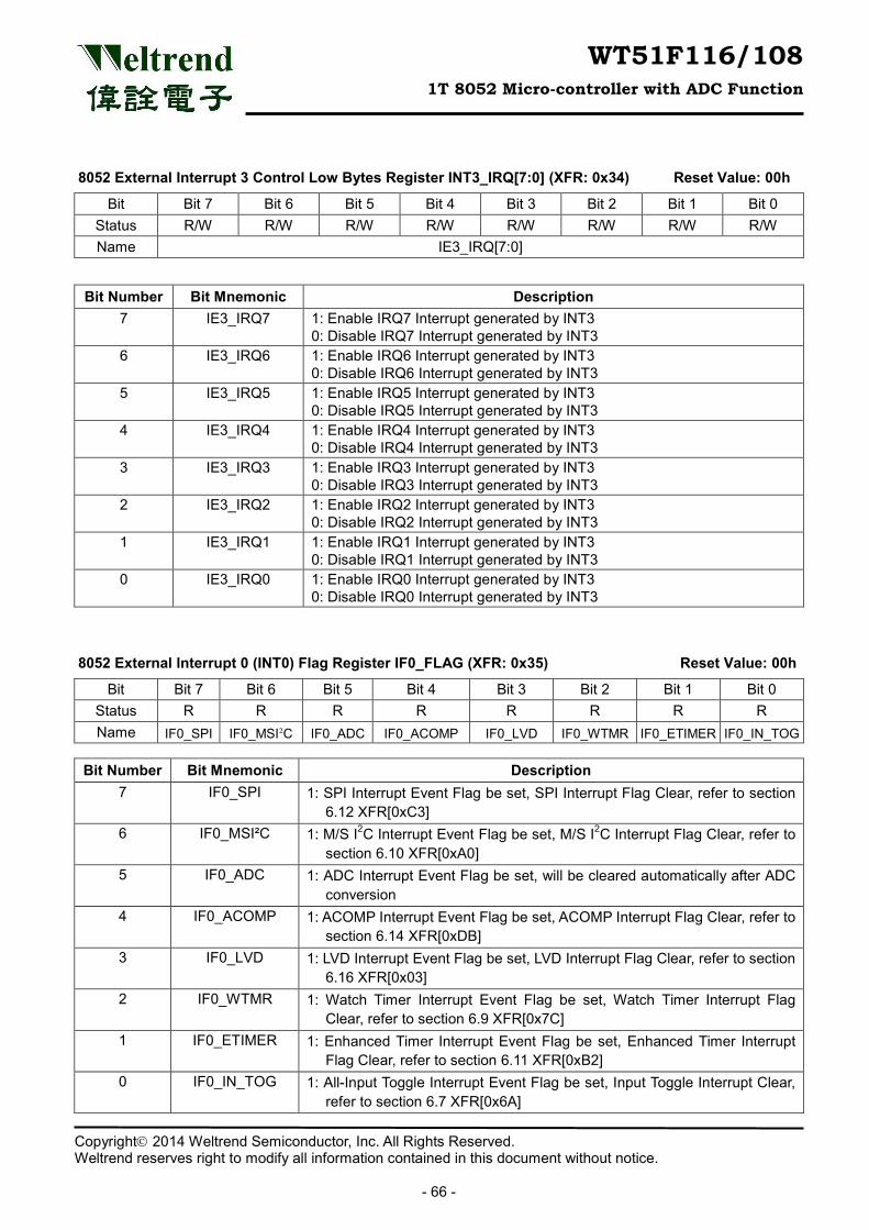
WT51F116/108 1T 8052 Micro-controller with ADC Function
Copyright 2014 Weltrend Semiconductor, Inc. All Rights Reserved. Weltrend reserves right to modify all information contained in this document without notice.
- 66 -
8052 External Interrupt 3 Control Low Bytes Register INT3_IRQ[7:0] (XFR: 0x34) Reset Value: 00h
Bit Bit 7 Bit 6 Bit 5 Bit 4 Bit 3 Bit 2 Bit 1 Bit 0 Status R/W R/W R/W R/W R/W R/W R/W R/W Name IE3_IRQ[7:0]
Bit Number Bit Mnemonic Description 7 IE3_IRQ7 1: Enable IRQ7 Interrupt generated by INT3
0: Disable IRQ7 Interrupt generated by INT3 6 IE3_IRQ6 1: Enable IRQ6 Interrupt generated by INT3
0: Disable IRQ6 Interrupt generated by INT3 5 IE3_IRQ5 1: Enable IRQ5 Interrupt generated by INT3
0: Disable IRQ5 Interrupt generated by INT3 4 IE3_IRQ4 1: Enable IRQ4 Interrupt generated by INT3
0: Disable IRQ4 Interrupt generated by INT3 3 IE3_IRQ3 1: Enable IRQ3 Interrupt generated by INT3
0: Disable IRQ3 Interrupt generated by INT3 2 IE3_IRQ2 1: Enable IRQ2 Interrupt generated by INT3
0: Disable IRQ2 Interrupt generated by INT3 1 IE3_IRQ1 1: Enable IRQ1 Interrupt generated by INT3
0: Disable IRQ1 Interrupt generated by INT3 0 IE3_IRQ0 1: Enable IRQ0 Interrupt generated by INT3
0: Disable IRQ0 Interrupt generated by INT3
8052 External Interrupt 0 (INT0) Flag Register IF0_FLAG (XFR: 0x35) Reset Value: 00h
Bit Bit 7 Bit 6 Bit 5 Bit 4 Bit 3 Bit 2 Bit 1 Bit 0 Status R R R R R R R R Name IF0_SPI IF0_MSI²C IF0_ADC IF0_ACOMP IF0_LVD IF0_WTMR IF0_ETIMER IF0_IN_TOG
Bit Number Bit Mnemonic Description
7 IF0_SPI 1: SPI Interrupt Event Flag be set, SPI Interrupt Flag Clear, refer to section 6.12 XFR[0xC3]
6 IF0_MSI²C 1: M/S I2C Interrupt Event Flag be set, M/S I2C Interrupt Flag Clear, refer to section 6.10 XFR[0xA0]
5 IF0_ADC 1: ADC Interrupt Event Flag be set, will be cleared automatically after ADC conversion
4 IF0_ACOMP 1: ACOMP Interrupt Event Flag be set, ACOMP Interrupt Flag Clear, refer to section 6.14 XFR[0xDB]
3 IF0_LVD 1: LVD Interrupt Event Flag be set, LVD Interrupt Flag Clear, refer to section 6.16 XFR[0x03]
2 IF0_WTMR 1: Watch Timer Interrupt Event Flag be set, Watch Timer Interrupt Flag Clear, refer to section 6.9 XFR[0x7C]
1 IF0_ETIMER 1: Enhanced Timer Interrupt Event Flag be set, Enhanced Timer Interrupt Flag Clear, refer to section 6.11 XFR[0xB2]
0 IF0_IN_TOG 1: All-Input Toggle Interrupt Event Flag be set, Input Toggle Interrupt Clear, refer to section 6.7 XFR[0x6A]
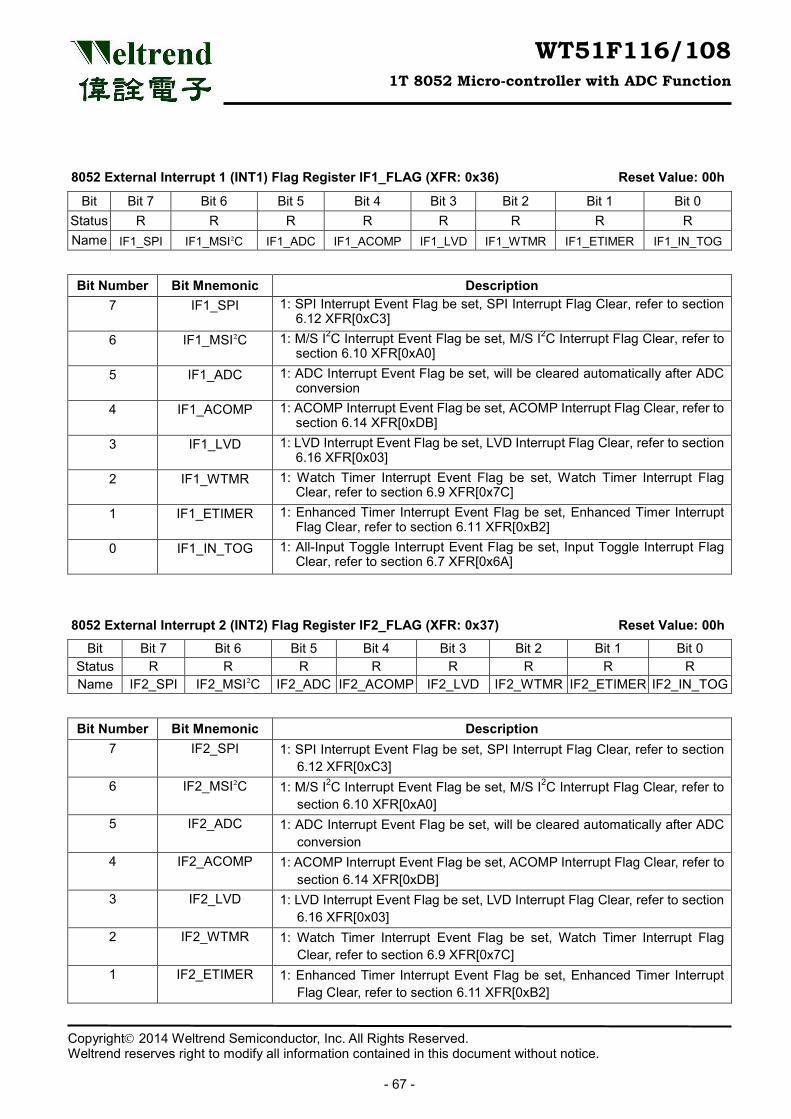
WT51F116/108 1T 8052 Micro-controller with ADC Function
Copyright 2014 Weltrend Semiconductor, Inc. All Rights Reserved. Weltrend reserves right to modify all information contained in this document without notice.
- 67 -
8052 External Interrupt 1 (INT1) Flag Register IF1_FLAG (XFR: 0x36) Reset Value: 00h
Bit Bit 7 Bit 6 Bit 5 Bit 4 Bit 3 Bit 2 Bit 1 Bit 0 Status R R R R R R R R Name IF1_SPI IF1_MSI²C IF1_ADC IF1_ACOMP IF1_LVD IF1_WTMR IF1_ETIMER IF1_IN_TOG
Bit Number Bit Mnemonic Description 7 IF1_SPI 1: SPI Interrupt Event Flag be set, SPI Interrupt Flag Clear, refer to section
6.12 XFR[0xC3] 6 IF1_MSI²C 1: M/S I2C Interrupt Event Flag be set, M/S I2C Interrupt Flag Clear, refer to
section 6.10 XFR[0xA0] 5 IF1_ADC 1: ADC Interrupt Event Flag be set, will be cleared automatically after ADC
conversion 4 IF1_ACOMP 1: ACOMP Interrupt Event Flag be set, ACOMP Interrupt Flag Clear, refer to
section 6.14 XFR[0xDB] 3 IF1_LVD 1: LVD Interrupt Event Flag be set, LVD Interrupt Flag Clear, refer to section
6.16 XFR[0x03] 2 IF1_WTMR 1: Watch Timer Interrupt Event Flag be set, Watch Timer Interrupt Flag
Clear, refer to section 6.9 XFR[0x7C] 1 IF1_ETIMER 1: Enhanced Timer Interrupt Event Flag be set, Enhanced Timer Interrupt
Flag Clear, refer to section 6.11 XFR[0xB2] 0 IF1_IN_TOG 1: All-Input Toggle Interrupt Event Flag be set, Input Toggle Interrupt Flag
Clear, refer to section 6.7 XFR[0x6A]
8052 External Interrupt 2 (INT2) Flag Register IF2_FLAG (XFR: 0x37) Reset Value: 00h
Bit Bit 7 Bit 6 Bit 5 Bit 4 Bit 3 Bit 2 Bit 1 Bit 0 Status R R R R R R R R Name IF2_SPI IF2_MSI²C IF2_ADC IF2_ACOMP IF2_LVD IF2_WTMR IF2_ETIMER IF2_IN_TOG
Bit Number Bit Mnemonic Description 7 IF2_SPI 1: SPI Interrupt Event Flag be set, SPI Interrupt Flag Clear, refer to section
6.12 XFR[0xC3] 6 IF2_MSI²C 1: M/S I2C Interrupt Event Flag be set, M/S I2C Interrupt Flag Clear, refer to
section 6.10 XFR[0xA0] 5 IF2_ADC 1: ADC Interrupt Event Flag be set, will be cleared automatically after ADC
conversion 4 IF2_ACOMP 1: ACOMP Interrupt Event Flag be set, ACOMP Interrupt Flag Clear, refer to
section 6.14 XFR[0xDB] 3 IF2_LVD 1: LVD Interrupt Event Flag be set, LVD Interrupt Flag Clear, refer to section
6.16 XFR[0x03] 2 IF2_WTMR 1: Watch Timer Interrupt Event Flag be set, Watch Timer Interrupt Flag
Clear, refer to section 6.9 XFR[0x7C] 1 IF2_ETIMER 1: Enhanced Timer Interrupt Event Flag be set, Enhanced Timer Interrupt
Flag Clear, refer to section 6.11 XFR[0xB2]
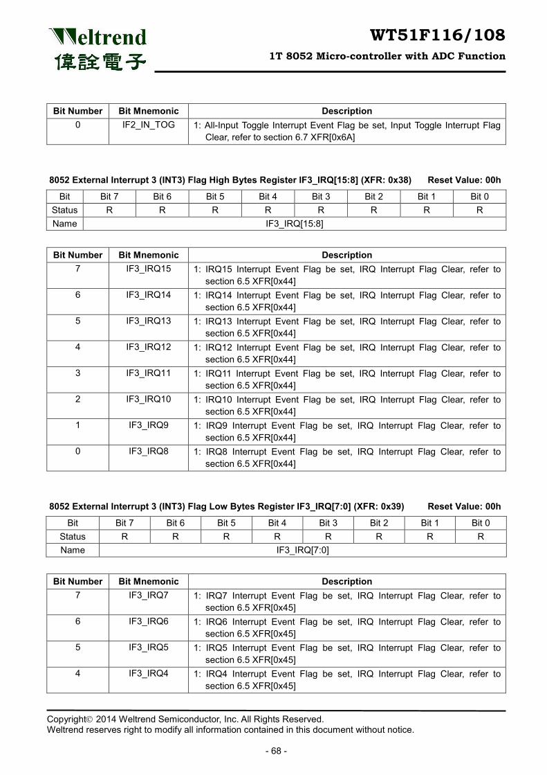
WT51F116/108 1T 8052 Micro-controller with ADC Function
Copyright 2014 Weltrend Semiconductor, Inc. All Rights Reserved. Weltrend reserves right to modify all information contained in this document without notice.
- 68 -
Bit Number Bit Mnemonic Description 0 IF2_IN_TOG 1: All-Input Toggle Interrupt Event Flag be set, Input Toggle Interrupt Flag
Clear, refer to section 6.7 XFR[0x6A]
8052 External Interrupt 3 (INT3) Flag High Bytes Register IF3_IRQ[15:8] (XFR: 0x38) Reset Value: 00h
Bit Bit 7 Bit 6 Bit 5 Bit 4 Bit 3 Bit 2 Bit 1 Bit 0 Status R R R R R R R R Name IF3_IRQ[15:8]
Bit Number Bit Mnemonic Description 7 IF3_IRQ15 1: IRQ15 Interrupt Event Flag be set, IRQ Interrupt Flag Clear, refer to
section 6.5 XFR[0x44] 6 IF3_IRQ14 1: IRQ14 Interrupt Event Flag be set, IRQ Interrupt Flag Clear, refer to
section 6.5 XFR[0x44] 5 IF3_IRQ13 1: IRQ13 Interrupt Event Flag be set, IRQ Interrupt Flag Clear, refer to
section 6.5 XFR[0x44] 4 IF3_IRQ12 1: IRQ12 Interrupt Event Flag be set, IRQ Interrupt Flag Clear, refer to
section 6.5 XFR[0x44] 3 IF3_IRQ11 1: IRQ11 Interrupt Event Flag be set, IRQ Interrupt Flag Clear, refer to
section 6.5 XFR[0x44] 2 IF3_IRQ10 1: IRQ10 Interrupt Event Flag be set, IRQ Interrupt Flag Clear, refer to
section 6.5 XFR[0x44] 1 IF3_IRQ9 1: IRQ9 Interrupt Event Flag be set, IRQ Interrupt Flag Clear, refer to
section 6.5 XFR[0x44] 0 IF3_IRQ8 1: IRQ8 Interrupt Event Flag be set, IRQ Interrupt Flag Clear, refer to
section 6.5 XFR[0x44]
8052 External Interrupt 3 (INT3) Flag Low Bytes Register IF3_IRQ[7:0] (XFR: 0x39) Reset Value: 00h
Bit Bit 7 Bit 6 Bit 5 Bit 4 Bit 3 Bit 2 Bit 1 Bit 0 Status R R R R R R R R Name IF3_IRQ[7:0]
Bit Number Bit Mnemonic Description 7 IF3_IRQ7 1: IRQ7 Interrupt Event Flag be set, IRQ Interrupt Flag Clear, refer to
section 6.5 XFR[0x45] 6 IF3_IRQ6 1: IRQ6 Interrupt Event Flag be set, IRQ Interrupt Flag Clear, refer to
section 6.5 XFR[0x45] 5 IF3_IRQ5 1: IRQ5 Interrupt Event Flag be set, IRQ Interrupt Flag Clear, refer to
section 6.5 XFR[0x45] 4 IF3_IRQ4 1: IRQ4 Interrupt Event Flag be set, IRQ Interrupt Flag Clear, refer to
section 6.5 XFR[0x45]
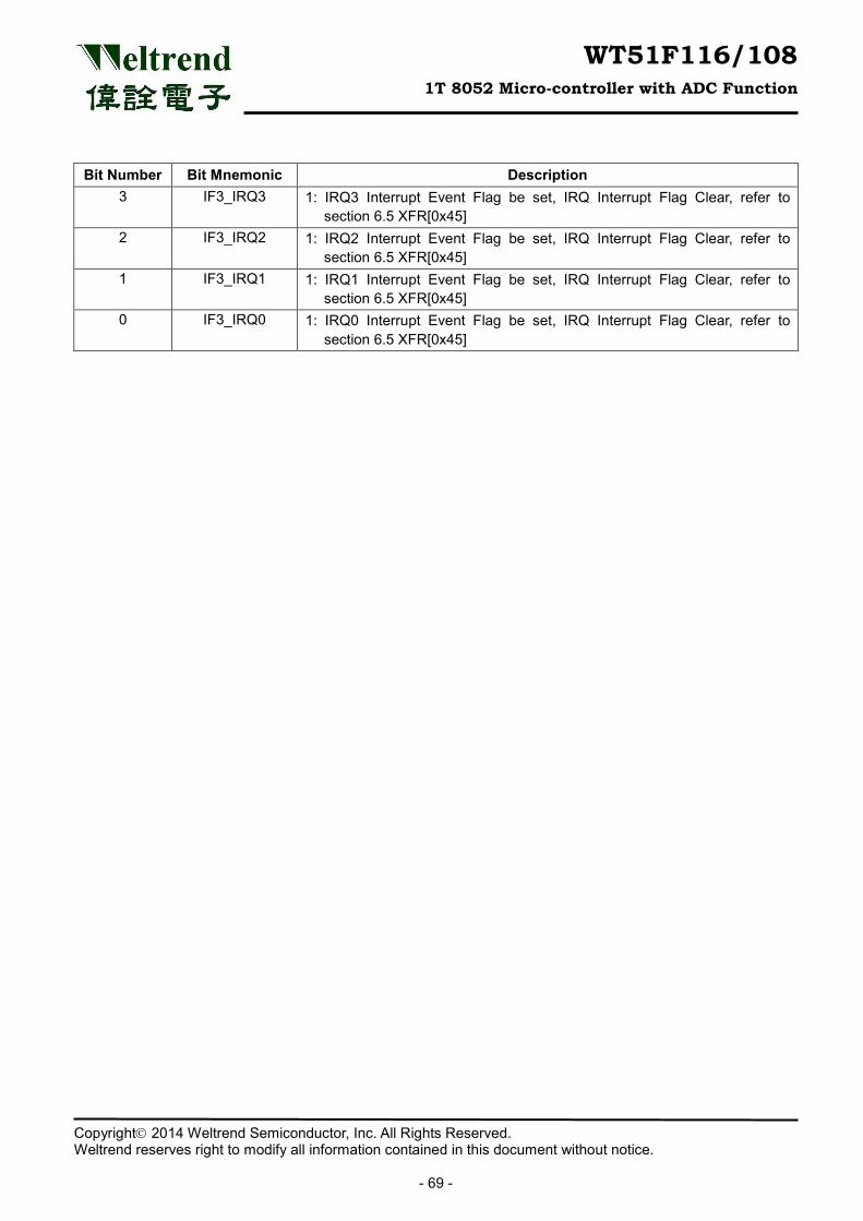
WT51F116/108 1T 8052 Micro-controller with ADC Function
Copyright 2014 Weltrend Semiconductor, Inc. All Rights Reserved. Weltrend reserves right to modify all information contained in this document without notice.
- 69 -
Bit Number Bit Mnemonic Description 3 IF3_IRQ3 1: IRQ3 Interrupt Event Flag be set, IRQ Interrupt Flag Clear, refer to
section 6.5 XFR[0x45] 2 IF3_IRQ2 1: IRQ2 Interrupt Event Flag be set, IRQ Interrupt Flag Clear, refer to
section 6.5 XFR[0x45] 1 IF3_IRQ1 1: IRQ1 Interrupt Event Flag be set, IRQ Interrupt Flag Clear, refer to
section 6.5 XFR[0x45] 0 IF3_IRQ0 1: IRQ0 Interrupt Event Flag be set, IRQ Interrupt Flag Clear, refer to
section 6.5 XFR[0x45]
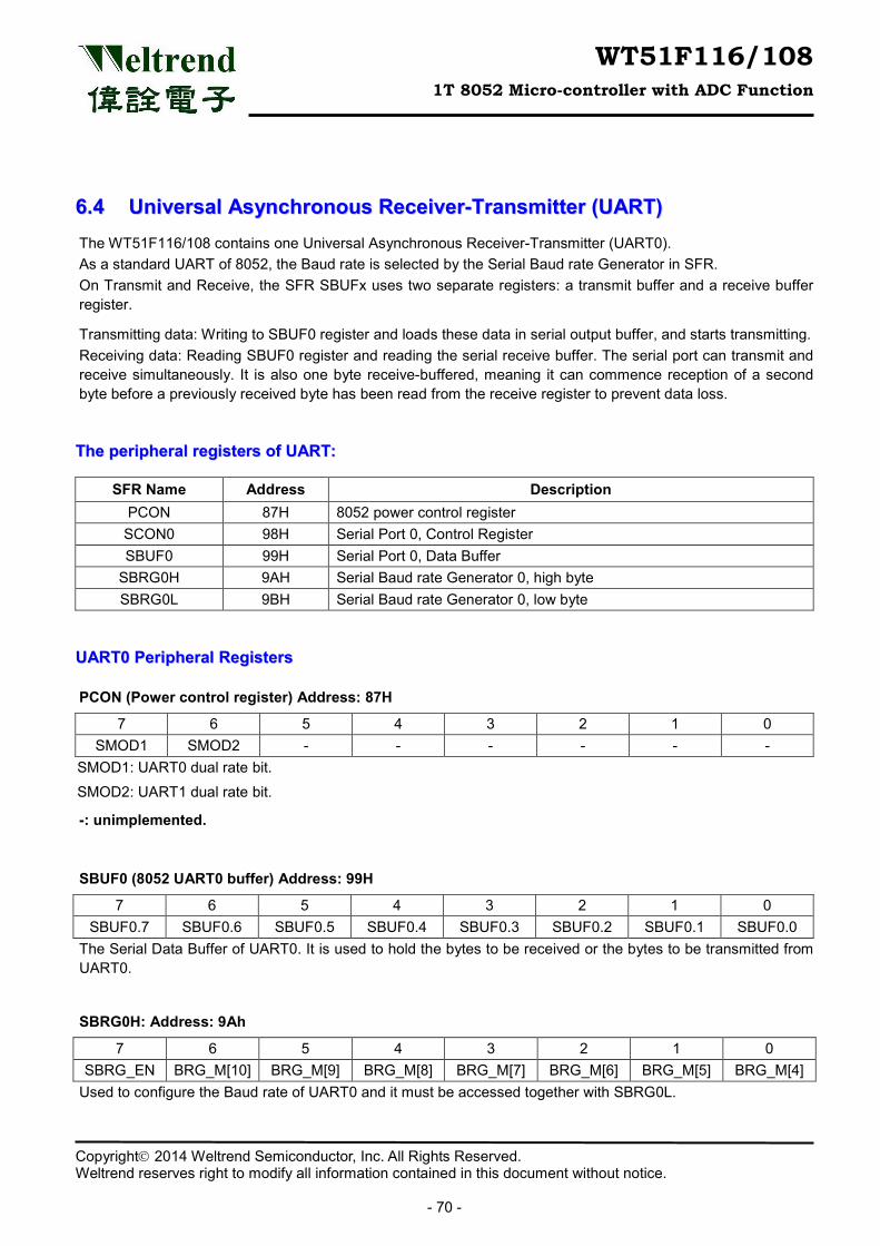
WT51F116/108 1T 8052 Micro-controller with ADC Function
Copyright 2014 Weltrend Semiconductor, Inc. All Rights Reserved. Weltrend reserves right to modify all information contained in this document without notice.
- 70 -
66..44 UUnniivveerrssaall AAssyynncchhrroonnoouuss RReecceeiivveerr--TTrraannssmmiitttteerr ((UUAARRTT)) The WT51F116/108 contains one Universal Asynchronous Receiver-Transmitter (UART0). As a standard UART of 8052, the Baud rate is selected by the Serial Baud rate Generator in SFR. On Transmit and Receive, the SFR SBUFx uses two separate registers: a transmit buffer and a receive buffer register.
Transmitting data: Writing to SBUF0 register and loads these data in serial output buffer, and starts transmitting. Receiving data: Reading SBUF0 register and reading the serial receive buffer. The serial port can transmit and receive simultaneously. It is also one byte receive-buffered, meaning it can commence reception of a second byte before a previously received byte has been read from the receive register to prevent data loss.
TThhee ppeerriipphheerraall rreeggiisstteerrss ooff UUAARRTT::
SFR Name Address Description PCON 87H 8052 power control register SCON0 98H Serial Port 0, Control Register SBUF0 99H Serial Port 0, Data Buffer
SBRG0H 9AH Serial Baud rate Generator 0, high byte SBRG0L 9BH Serial Baud rate Generator 0, low byte
UUAARRTT00 PPeerriipphheerraall RReeggiisstteerrss
PCON (Power control register) Address: 87H
7 6 5 4 3 2 1 0 SMOD1 SMOD2 - - - - - -
SMOD1: UART0 dual rate bit. SMOD2: UART1 dual rate bit.
-: unimplemented.
SBUF0 (8052 UART0 buffer) Address: 99H
7 6 5 4 3 2 1 0 SBUF0.7 SBUF0.6 SBUF0.5 SBUF0.4 SBUF0.3 SBUF0.2 SBUF0.1 SBUF0.0
The Serial Data Buffer of UART0. It is used to hold the bytes to be received or the bytes to be transmitted from UART0.
SBRG0H: Address: 9Ah
7 6 5 4 3 2 1 0 SBRG_EN BRG_M[10] BRG_M[9] BRG_M[8] BRG_M[7] BRG_M[6] BRG_M[5] BRG_M[4]
Used to configure the Baud rate of UART0 and it must be accessed together with SBRG0L.
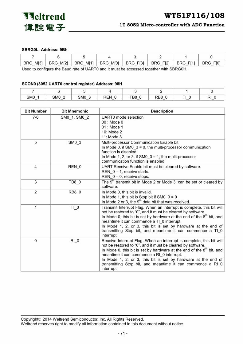
WT51F116/108 1T 8052 Micro-controller with ADC Function
Copyright 2014 Weltrend Semiconductor, Inc. All Rights Reserved. Weltrend reserves right to modify all information contained in this document without notice.
- 71 -
SBRG0L: Address: 9Bh
7 6 5 4 3 2 1 0 BRG_M[3] BRG_M[2] BRG_M[1] BRG_M[0] BRG_F[3] BRG_F[2] BRG_F[1] BRG_F[0]
Used to configure the Baud rate of UART0 and it must be accessed together with SBRG0H.
SCON0 (8052 UART0 control register) Address: 98H
7 6 5 4 3 2 1 0 SM0_1 SM0_2 SM0_3 REN_0 TB8_0 RB8_0 TI_0 RI_0
Bit Number Bit Mnemonic Description 7-6 SM0_1, SM0_2 UART0 mode selection
00 : Mode 0 01 : Mode 1 10: Mode 2 11: Mode 3
5 SM0_3 Multi-processor Communication Enable bit In Mode 0, if SM0_3 = 0, the multi-processor communication function is disabled. In Mode 1, 2, or 3, if SM0_3 = 1, the multi-processor communication function is enabled.
4 REN_0 UART Receive Enable bit must be cleared by software. REN_0 = 1, receive starts. REN_0 = 0, receive stops.
3 TB8_0 The 9th transmit bit in Mode 2 or Mode 3, can be set or cleared by software.
2 RB8_0 In Mode 0, this bit is invalid. In Mode 1, this bit is Stop bit if SM0_3 = 0 In Mode 2 or 3, the 9th data bit that was received.
1 TI_0 Transmit Interrupt Flag. When an interrupt is complete, this bit will not be restored to “0”, and it must be cleared by software. In Mode 0, this bit is set by hardware at the end of the 8th bit, and meantime it can commence a TI_0 interrupt. In Mode 1, 2, or 3, this bit is set by hardware at the end of transmitting Stop bit, and meantime it can commence a TI_0 interrupt.
0 RI_0 Receive Interrupt Flag. When an interrupt is complete, this bit will not be restored to “0”, and it must be cleared by software. In Mode 0, this bit is set by hardware at the end of the 8th bit, and meantime it can commence a RI_0 interrupt. In Mode 1, 2, or 3, this bit is set by hardware at the end of transmitting Stop bit, and meantime it can commence a RI_0 interrupt.
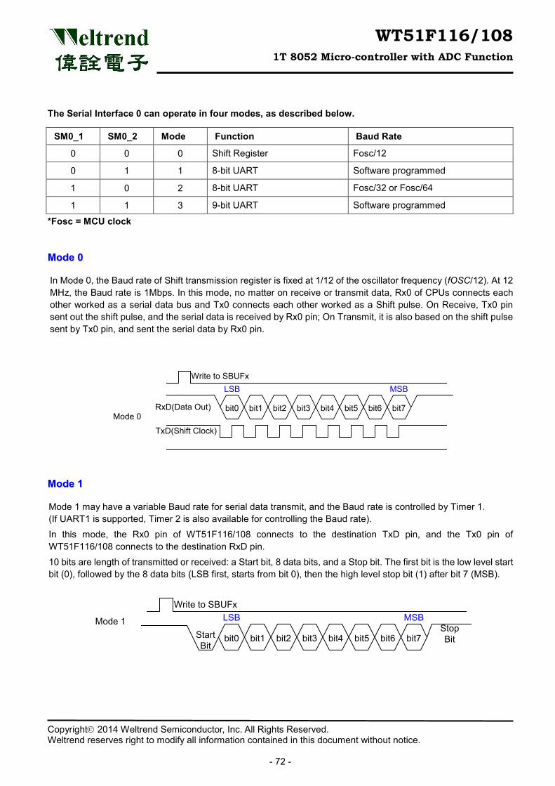
WT51F116/108 1T 8052 Micro-controller with ADC Function
Copyright 2014 Weltrend Semiconductor, Inc. All Rights Reserved. Weltrend reserves right to modify all information contained in this document without notice.
- 72 -
The Serial Interface 0 can operate in four modes, as described below.
SM0_1 SM0_2 Mode Function Baud Rate
0 0 0 Shift Register Fosc/12
0 1 1 8-bit UART Software programmed
1 0 2 8-bit UART Fosc/32 or Fosc/64
1 1 3 9-bit UART Software programmed
*Fosc = MCU clock
MMooddee 00
In Mode 0, the Baud rate of Shift transmission register is fixed at 1/12 of the oscillator frequency (fOSC/12). At 12 MHz, the Baud rate is 1Mbps. In this mode, no matter on receive or transmit data, Rx0 of CPUs connects each other worked as a serial data bus and Tx0 connects each other worked as a Shift pulse. On Receive, Tx0 pin sent out the shift pulse, and the serial data is received by Rx0 pin; On Transmit, it is also based on the shift pulse sent by Tx0 pin, and sent the serial data by Rx0 pin.
Write to SBUFx
TxD(Shift Clock)
RxD(Data Out) bit0 bit1 bit2 bit3 bit4 bit5 bit6 bit7
MSBLSB
Mode 0
MMooddee 11
Mode 1 may have a variable Baud rate for serial data transmit, and the Baud rate is controlled by Timer 1. (If UART1 is supported, Timer 2 is also available for controlling the Baud rate). In this mode, the Rx0 pin of WT51F116/108 connects to the destination TxD pin, and the Tx0 pin of WT51F116/108 connects to the destination RxD pin. 10 bits are length of transmitted or received: a Start bit, 8 data bits, and a Stop bit. The first bit is the low level start bit (0), followed by the 8 data bits (LSB first, starts from bit 0), then the high level stop bit (1) after bit 7 (MSB).
Write to SBUFx
bit0 bit1 bit2 bit3 bit4 bit5 bit6 bit7StartBit
Stop Bit
MSBLSBMode 1
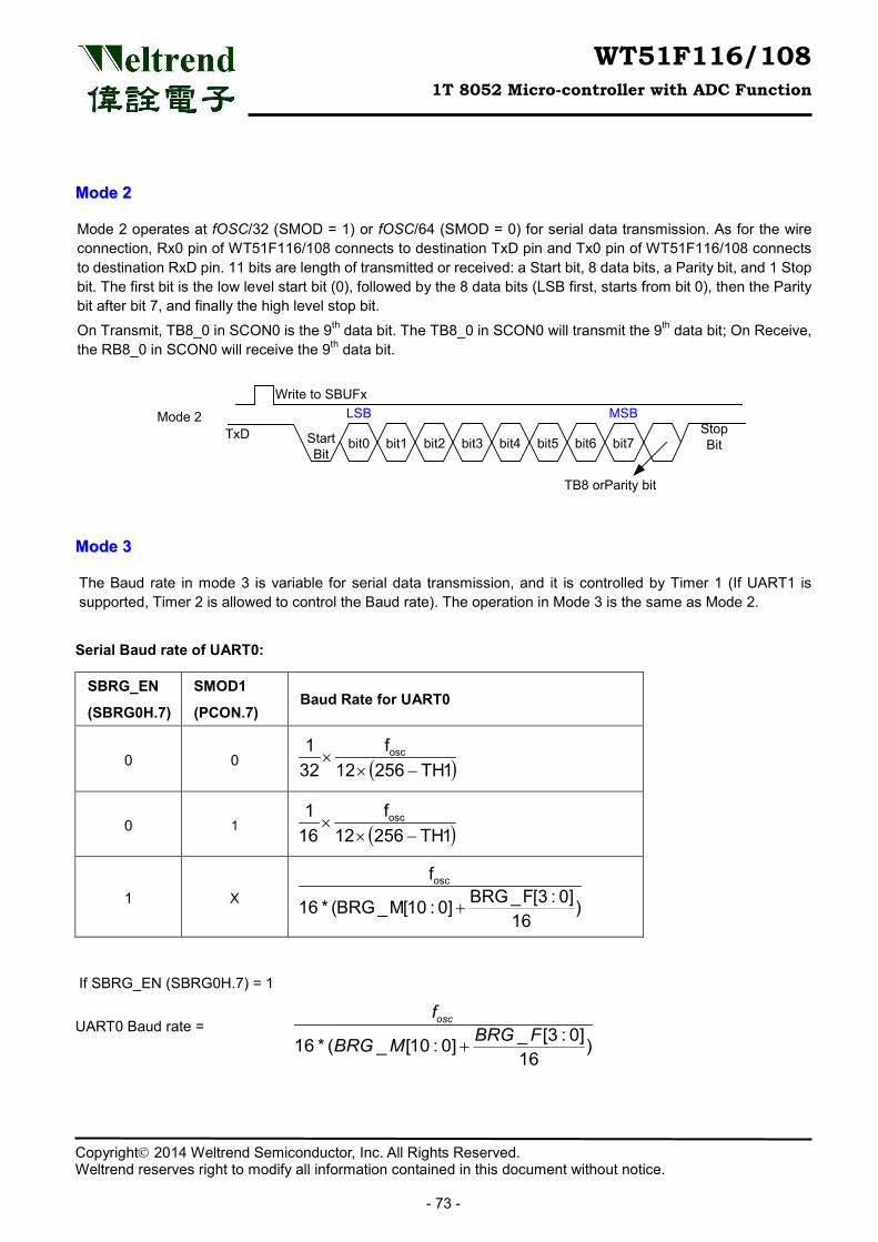
WT51F116/108 1T 8052 Micro-controller with ADC Function
Copyright 2014 Weltrend Semiconductor, Inc. All Rights Reserved. Weltrend reserves right to modify all information contained in this document without notice.
- 73 -
MMooddee 22
Mode 2 operates at fOSC/32 (SMOD = 1) or fOSC/64 (SMOD = 0) for serial data transmission. As for the wire connection, Rx0 pin of WT51F116/108 connects to destination TxD pin and Tx0 pin of WT51F116/108 connects to destination RxD pin. 11 bits are length of transmitted or received: a Start bit, 8 data bits, a Parity bit, and 1 Stop bit. The first bit is the low level start bit (0), followed by the 8 data bits (LSB first, starts from bit 0), then the Parity bit after bit 7, and finally the high level stop bit.
On Transmit, TB8_0 in SCON0 is the 9th data bit. The TB8_0 in SCON0 will transmit the 9th data bit; On Receive, the RB8_0 in SCON0 will receive the 9th data bit.
Write to SBUFx
TxDbit0 bit1 bit2 bit3 bit4 bit5 bit6 bit7Start
Bit
Stop Bit
MSBLSBMode 2
TB8 orParity bit
MMooddee 33
The Baud rate in mode 3 is variable for serial data transmission, and it is controlled by Timer 1 (If UART1 is supported, Timer 2 is allowed to control the Baud rate). The operation in Mode 3 is the same as Mode 2.
Serial Baud rate of UART0:
SBRG_EN
(SBRG0H.7)
SMOD1
(PCON.7) Baud Rate for UART0
0 0 ( )1TH25612f
321 osc
−××
0 1 ( )1TH25612f
161 osc
−××
1 X )16
]0:3[F_BRG]0:10[M_BRG(*16
fosc
+
If SBRG_EN (SBRG0H.7) = 1 UART0 Baud rate =
+_ [3 : 0]16 * ( _ [10 : 0] )16
oscfBRG FBRG M
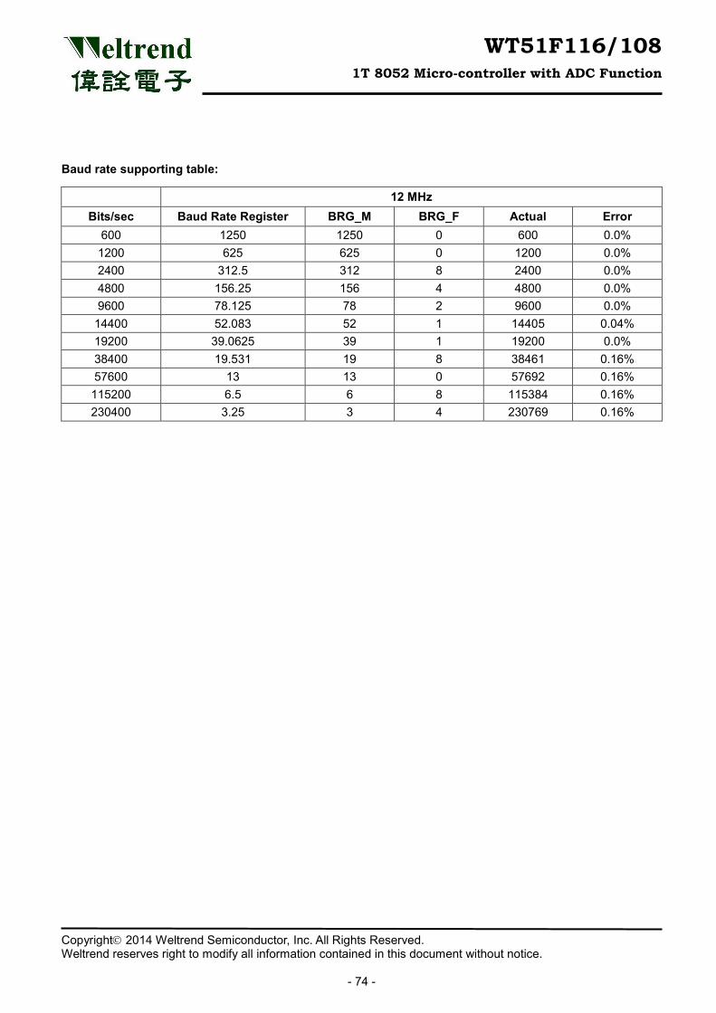
WT51F116/108 1T 8052 Micro-controller with ADC Function
Copyright 2014 Weltrend Semiconductor, Inc. All Rights Reserved. Weltrend reserves right to modify all information contained in this document without notice.
- 74 -
Baud rate supporting table:
12 MHz Bits/sec Baud Rate Register BRG_M BRG_F Actual Error
600 1250 1250 0 600 0.0% 1200 625 625 0 1200 0.0% 2400 312.5 312 8 2400 0.0% 4800 156.25 156 4 4800 0.0% 9600 78.125 78 2 9600 0.0%
14400 52.083 52 1 14405 0.04% 19200 39.0625 39 1 19200 0.0% 38400 19.531 19 8 38461 0.16% 57600 13 13 0 57692 0.16% 115200 6.5 6 8 115384 0.16% 230400 3.25 3 4 230769 0.16%
WT51F116/108 1T 8052 Micro-controller with ADC Function
Copyright 2014 Weltrend Semiconductor, Inc. All Rights Reserved. Weltrend reserves right to modify all information contained in this document without notice.
- 75 -
66..55 EExxtteerrnnaall IInntteerrrruupptt RReeqquueesstt ((IIRRQQ)) Supports 16 input Interrupts and built-in digital Filter. (The clock source of digital filer is internal oscillator
12 MHz) Supports single-side positive edge-triggered, negative edge-triggered, or positive edge and negative edge
triggered simultaneously It can work with PWM, applied on motor RPM (Revolutions Per Minute) Control. Please refer to the table
below.
External Interrupt Request (IRQ) & PWM0 mapping table:
External Interrupt Request (IRQ) pin PWM0 Output pin
IRQ10 Path A GPIOB3
IRQ14 Path B GPIOA4
IRQ0 Path C GPIOA0
IRQ5 Path D GPIOB2
External Interrupt Request (IRQ) & PWM1 mapping table:
External Interrupt Request (IRQ) pin PWM1 Output pin
IRQ12 Path A GPIOB5
IRQ15 Path B GPIOA5
IRQ2 Path C GPIOA2
IRQ11 Path D GPIOB4
External Interrupt Request (IRQ) & PWM2 mapping table:
External Interrupt Request (IRQ) pin PWM1 Output pin
IRQ3 Path A GPIOB0
IRQ1 Path B GPIOA1
- Path C GPIOC2
External Interrupt Request (IRQ) & PWM3 mapping table:
External Interrupt Request (IRQ) pin PWM1 Output pin
IRQ4 Path A GPIOB1
IRQ6 Path B GPIOC0
- Path C GPIOC3
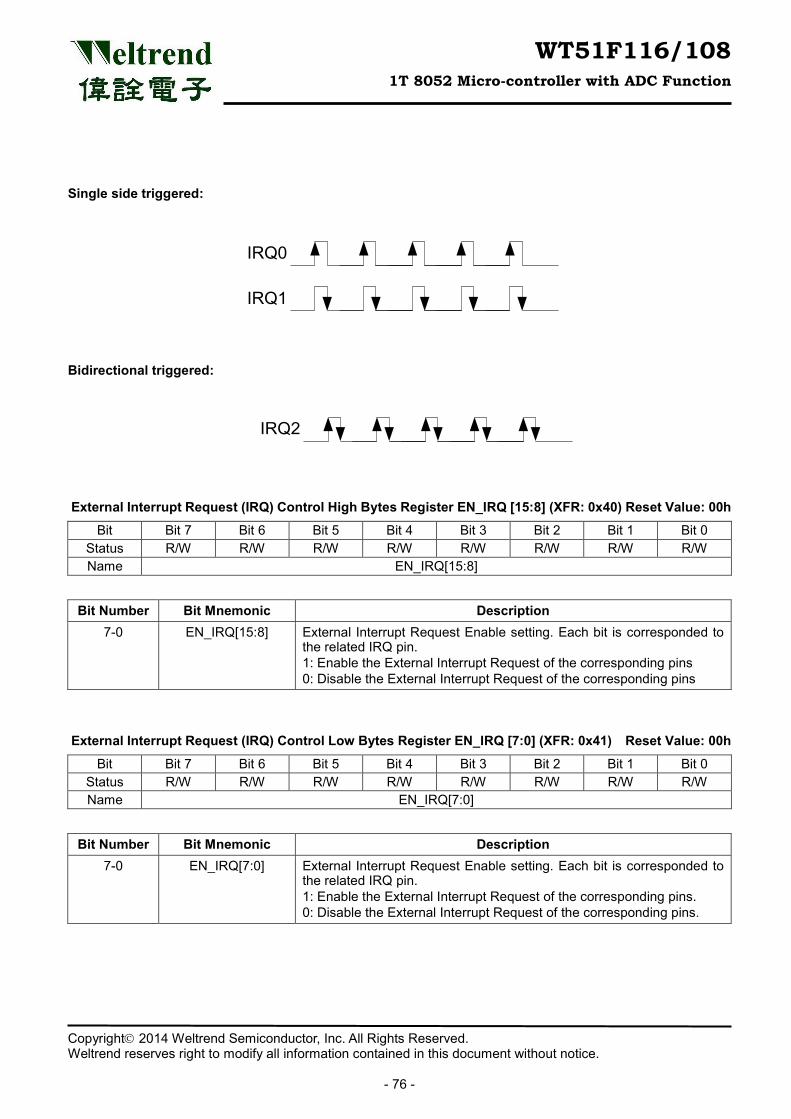
WT51F116/108 1T 8052 Micro-controller with ADC Function
Copyright 2014 Weltrend Semiconductor, Inc. All Rights Reserved. Weltrend reserves right to modify all information contained in this document without notice.
- 76 -
Single side triggered:
IRQ0
IRQ1
Bidirectional triggered:
IRQ2
External Interrupt Request (IRQ) Control High Bytes Register EN_IRQ [15:8] (XFR: 0x40) Reset Value: 00h
Bit Bit 7 Bit 6 Bit 5 Bit 4 Bit 3 Bit 2 Bit 1 Bit 0 Status R/W R/W R/W R/W R/W R/W R/W R/W Name EN_IRQ[15:8]
Bit Number Bit Mnemonic Description 7-0 EN_IRQ[15:8] External Interrupt Request Enable setting. Each bit is corresponded to
the related IRQ pin. 1: Enable the External Interrupt Request of the corresponding pins 0: Disable the External Interrupt Request of the corresponding pins
External Interrupt Request (IRQ) Control Low Bytes Register EN_IRQ [7:0] (XFR: 0x41) Reset Value: 00h
Bit Bit 7 Bit 6 Bit 5 Bit 4 Bit 3 Bit 2 Bit 1 Bit 0 Status R/W R/W R/W R/W R/W R/W R/W R/W Name EN_IRQ[7:0]
Bit Number Bit Mnemonic Description 7-0 EN_IRQ[7:0] External Interrupt Request Enable setting. Each bit is corresponded to
the related IRQ pin. 1: Enable the External Interrupt Request of the corresponding pins. 0: Disable the External Interrupt Request of the corresponding pins.
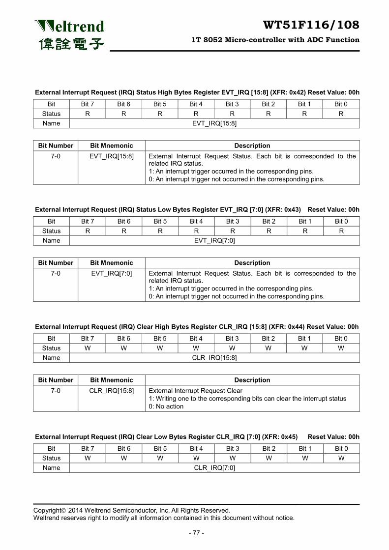
WT51F116/108 1T 8052 Micro-controller with ADC Function
Copyright 2014 Weltrend Semiconductor, Inc. All Rights Reserved. Weltrend reserves right to modify all information contained in this document without notice.
- 77 -
External Interrupt Request (IRQ) Status High Bytes Register EVT_IRQ [15:8] (XFR: 0x42) Reset Value: 00h
Bit Bit 7 Bit 6 Bit 5 Bit 4 Bit 3 Bit 2 Bit 1 Bit 0 Status R R R R R R R R Name EVT_IRQ[15:8]
Bit Number Bit Mnemonic Description 7-0 EVT_IRQ[15:8] External Interrupt Request Status. Each bit is corresponded to the
related IRQ status. 1: An interrupt trigger occurred in the corresponding pins. 0: An interrupt trigger not occurred in the corresponding pins.
External Interrupt Request (IRQ) Status Low Bytes Register EVT_IRQ [7:0] (XFR: 0x43) Reset Value: 00h
Bit Bit 7 Bit 6 Bit 5 Bit 4 Bit 3 Bit 2 Bit 1 Bit 0 Status R R R R R R R R Name EVT_IRQ[7:0]
Bit Number Bit Mnemonic Description 7-0 EVT_IRQ[7:0] External Interrupt Request Status. Each bit is corresponded to the
related IRQ status. 1: An interrupt trigger occurred in the corresponding pins. 0: An interrupt trigger not occurred in the corresponding pins.
External Interrupt Request (IRQ) Clear High Bytes Register CLR_IRQ [15:8] (XFR: 0x44) Reset Value: 00h
Bit Bit 7 Bit 6 Bit 5 Bit 4 Bit 3 Bit 2 Bit 1 Bit 0 Status W W W W W W W W Name CLR_IRQ[15:8]
Bit Number Bit Mnemonic Description 7-0 CLR_IRQ[15:8] External Interrupt Request Clear
1: Writing one to the corresponding bits can clear the interrupt status 0: No action
External Interrupt Request (IRQ) Clear Low Bytes Register CLR_IRQ [7:0] (XFR: 0x45) Reset Value: 00h
Bit Bit 7 Bit 6 Bit 5 Bit 4 Bit 3 Bit 2 Bit 1 Bit 0 Status W W W W W W W W Name CLR_IRQ[7:0]
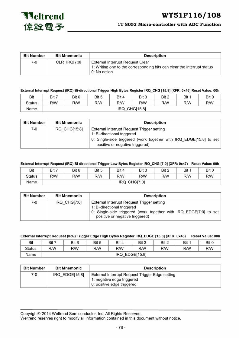
WT51F116/108 1T 8052 Micro-controller with ADC Function
Copyright 2014 Weltrend Semiconductor, Inc. All Rights Reserved. Weltrend reserves right to modify all information contained in this document without notice.
- 78 -
Bit Number Bit Mnemonic Description 7-0 CLR_IRQ[7:0] External Interrupt Request Clear
1: Writing one to the corresponding bits can clear the interrupt status 0: No action
External Interrupt Request (IRQ) Bi-directional Trigger High Bytes Register IRQ_CHG [15:8] (XFR: 0x46) Reset Value: 00h
Bit Bit 7 Bit 6 Bit 5 Bit 4 Bit 3 Bit 2 Bit 1 Bit 0 Status R/W R/W R/W R/W R/W R/W R/W R/W Name IRQ_CHG[15:8]
Bit Number Bit Mnemonic Description 7-0 IRQ_CHG[15:8] External Interrupt Request Trigger setting
1: Bi-directional triggered 0: Single-side triggered (work together with IRQ_EDGE[15:8] to set
positive or negative triggered)
External Interrupt Request (IRQ) Bi-directional Trigger Low Bytes Register IRQ_CHG [7:0] (XFR: 0x47) Reset Value: 00h
Bit Bit 7 Bit 6 Bit 5 Bit 4 Bit 3 Bit 2 Bit 1 Bit 0 Status R/W R/W R/W R/W R/W R/W R/W R/W Name IRQ_CHG[7:0]
Bit Number Bit Mnemonic Description 7-0 IRQ_CHG[7:0] External Interrupt Request Trigger setting
1: Bi-directional triggered 0: Single-side triggered (work together with IRQ_EDGE[7:0] to set
positive or negative triggered)
External Interrupt Request (IRQ) Trigger Edge High Bytes Register IRQ_EDGE [15:8] (XFR: 0x48) Reset Value: 00h
Bit Bit 7 Bit 6 Bit 5 Bit 4 Bit 3 Bit 2 Bit 1 Bit 0 Status R/W R/W R/W R/W R/W R/W R/W R/W Name IRQ_EDGE[15:8]
Bit Number Bit Mnemonic Description 7-0 IRQ_EDGE[15:8] External Interrupt Request Trigger Edge setting
1: negative edge triggered 0: positive edge triggered
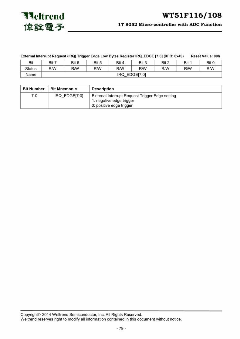
WT51F116/108 1T 8052 Micro-controller with ADC Function
Copyright 2014 Weltrend Semiconductor, Inc. All Rights Reserved. Weltrend reserves right to modify all information contained in this document without notice.
- 79 -
External Interrupt Request (IRQ) Trigger Edge Low Bytes Register IRQ_EDGE [7:0] (XFR: 0x49) Reset Value: 00h
Bit Bit 7 Bit 6 Bit 5 Bit 4 Bit 3 Bit 2 Bit 1 Bit 0 Status R/W R/W R/W R/W R/W R/W R/W R/W Name IRQ_EDGE[7:0]
Bit Number Bit Mnemonic Description 7-0 IRQ_EDGE[7:0] External Interrupt Request Trigger Edge setting
1: negative edge trigger 0: positive edge trigger
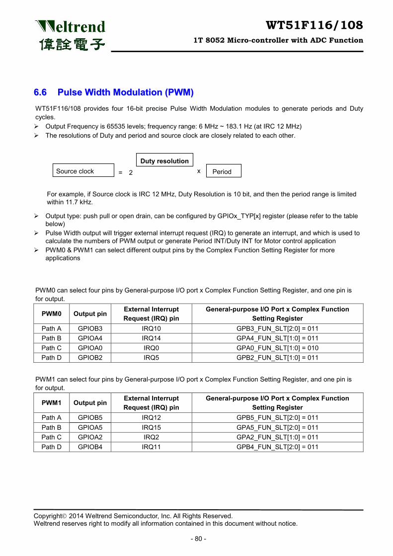
WT51F116/108 1T 8052 Micro-controller with ADC Function
Copyright 2014 Weltrend Semiconductor, Inc. All Rights Reserved. Weltrend reserves right to modify all information contained in this document without notice.
- 80 -
66..66 PPuullssee WWiiddtthh MMoodduullaattiioonn ((PPWWMM)) WT51F116/108 provides four 16-bit precise Pulse Width Modulation modules to generate periods and Duty cycles. Output Frequency is 65535 levels; frequency range: 6 MHz ~ 183.1 Hz (at IRC 12 MHz) The resolutions of Duty and period and source clock are closely related to each other.
For example, if Source clock is IRC 12 MHz, Duty Resolution is 10 bit, and then the period range is limited within 11.7 kHz.
Output type: push pull or open drain, can be configured by GPIOx_TYP[x] register (please refer to the table below)
Pulse Width output will trigger external interrupt request (IRQ) to generate an interrupt, and which is used to calculate the numbers of PWM output or generate Period INT/Duty INT for Motor control application
PWM0 & PWM1 can select different output pins by the Complex Function Setting Register for more applications
PWM0 can select four pins by General-purpose I/O port x Complex Function Setting Register, and one pin is for output.
PWM0 Output pin External Interrupt Request (IRQ) pin
General-purpose I/O Port x Complex Function Setting Register
Path A GPIOB3 IRQ10 GPB3_FUN_SLT[2:0] = 011 Path B GPIOA4 IRQ14 GPA4_FUN_SLT[1:0] = 011 Path C GPIOA0 IRQ0 GPA0_FUN_SLT[1:0] = 010 Path D GPIOB2 IRQ5 GPB2_FUN_SLT[1:0] = 011
PWM1 can select four pins by General-purpose I/O port x Complex Function Setting Register, and one pin is for output.
PWM1 Output pin External Interrupt Request (IRQ) pin
General-purpose I/O Port x Complex Function Setting Register
Path A GPIOB5 IRQ12 GPB5_FUN_SLT[2:0] = 011 Path B GPIOA5 IRQ15 GPA5_FUN_SLT[2:0] = 011 Path C GPIOA2 IRQ2 GPA2_FUN_SLT[1:0] = 011 Path D GPIOB4 IRQ11 GPB4_FUN_SLT[2:0] = 011
Source clock = 2 x
Duty resolution
Period
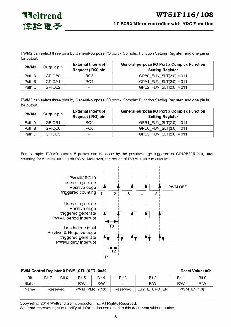
WT51F116/108 1T 8052 Micro-controller with ADC Function
Copyright 2014 Weltrend Semiconductor, Inc. All Rights Reserved. Weltrend reserves right to modify all information contained in this document without notice.
- 81 -
PWM2 can select three pins by General-purpose I/O port x Complex Function Setting Register, and one pin is for output.
PWM2 Output pin External Interrupt Request (IRQ) pin
General-purpose I/O Port x Complex Function Setting Register
Path A GPIOB0 IRQ3 GPB0_FUN_SLT[2:0] = 011 Path B GPIOA1 IRQ1 GPA1_FUN_SLT[2:0] = 011 Path C GPIOC2 - GPC2_FUN_SLT[2:0] = 011
PWM3 can select three pins by General-purpose I/O port x Complex Function Setting Register, and one pin is for output.
PWM3 Output pin External Interrupt Request (IRQ) pin
General-purpose I/O Port x Complex Function Setting Register
Path A GPIOB1 IRQ4 GPB1_FUN_SLT[2:0] = 011 Path B GPIOC0 IRQ6 GPC0_FUN_SLT[2:0] = 011 Path C GPIOC3 - GPC3_FUN_SLT[2:0] = 011
For example, PWM0 outputs 5 pulses can be done by the positive-edge triggered of GPIOB3/IRQ10, after counting for 5 times, turning off PWM. Moreover, the period of PWM is able to calculate.
1 2 3 4 5
PWM0/IRQ10 uses single-side
Positive-edge triggered counting
T1T2
PWM OFF
Uses single-side Positive-edge
triggered generate PWM0 period Interrupt
T0Uses bidirectionalPositive & Negative edge
triggered generate PWM0 duty Interrupt
PWM Control Register 0 PWM_CTL (XFR: 0x50) Reset Value: 00h
Bit Bit 7 Bit 6 Bit 5 Bit 4 Bit 3 Bit 2 Bit 1 Bit 0 Status - - R/W R/W - R/W R/W R/W Name Reserved PWM_PLRTY[1:0] Reserved LBYTE_UPD_EN PWM_EN[1:0]
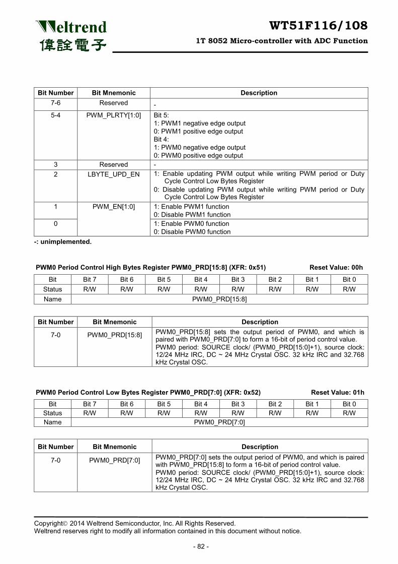
WT51F116/108 1T 8052 Micro-controller with ADC Function
Copyright 2014 Weltrend Semiconductor, Inc. All Rights Reserved. Weltrend reserves right to modify all information contained in this document without notice.
- 82 -
Bit Number Bit Mnemonic Description 7-6 Reserved - 5-4 PWM_PLRTY[1:0] Bit 5:
1: PWM1 negative edge output 0: PWM1 positive edge output Bit 4: 1: PWM0 negative edge output 0: PWM0 positive edge output
3 Reserved - 2 LBYTE_UPD_EN 1: Enable updating PWM output while writing PWM period or Duty
Cycle Control Low Bytes Register 0: Disable updating PWM output while writing PWM period or Duty
Cycle Control Low Bytes Register 1 PWM_EN[1:0] 1: Enable PWM1 function
0: Disable PWM1 function 0 1: Enable PWM0 function
0: Disable PWM0 function -: unimplemented.
PWM0 Period Control High Bytes Register PWM0_PRD[15:8] (XFR: 0x51) Reset Value: 00h
Bit Bit 7 Bit 6 Bit 5 Bit 4 Bit 3 Bit 2 Bit 1 Bit 0 Status R/W R/W R/W R/W R/W R/W R/W R/W Name PWM0_PRD[15:8]
Bit Number Bit Mnemonic Description
7-0 PWM0_PRD[15:8] PWM0_PRD[15:8] sets the output period of PWM0, and which is paired with PWM0_PRD[7:0] to form a 16-bit of period control value. PWM0 period: SOURCE clock/ (PWM0_PRD[15:0]+1), source clock: 12/24 MHz IRC, DC ~ 24 MHz Crystal OSC. 32 kHz IRC and 32.768 kHz Crystal OSC.
PWM0 Period Control Low Bytes Register PWM0_PRD[7:0] (XFR: 0x52) Reset Value: 01h
Bit Bit 7 Bit 6 Bit 5 Bit 4 Bit 3 Bit 2 Bit 1 Bit 0 Status R/W R/W R/W R/W R/W R/W R/W R/W Name PWM0_PRD[7:0]
Bit Number Bit Mnemonic Description
7-0 PWM0_PRD[7:0] PWM0_PRD[7:0] sets the output period of PWM0, and which is paired with PWM0_PRD[15:8] to form a 16-bit of period control value. PWM0 period: SOURCE clock/ (PWM0_PRD[15:0]+1), source clock: 12/24 MHz IRC, DC ~ 24 MHz Crystal OSC. 32 kHz IRC and 32.768 kHz Crystal OSC.
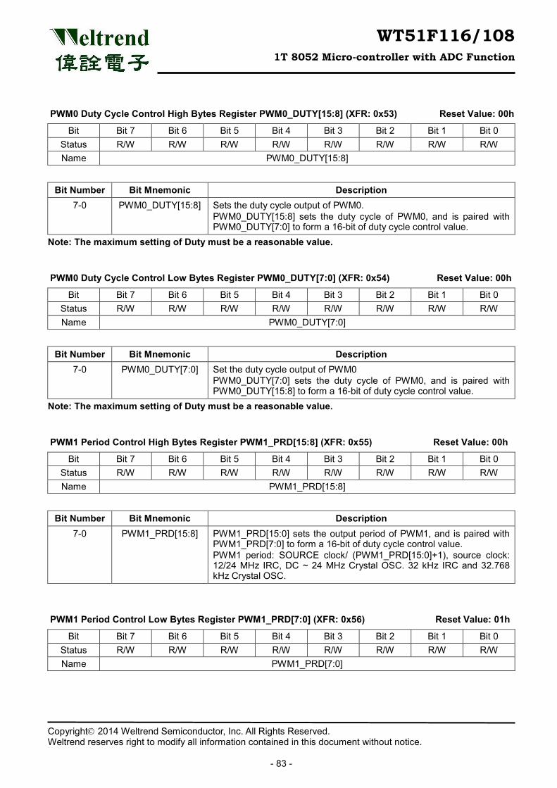
WT51F116/108 1T 8052 Micro-controller with ADC Function
Copyright 2014 Weltrend Semiconductor, Inc. All Rights Reserved. Weltrend reserves right to modify all information contained in this document without notice.
- 83 -
PWM0 Duty Cycle Control High Bytes Register PWM0_DUTY[15:8] (XFR: 0x53) Reset Value: 00h
Bit Bit 7 Bit 6 Bit 5 Bit 4 Bit 3 Bit 2 Bit 1 Bit 0 Status R/W R/W R/W R/W R/W R/W R/W R/W Name PWM0_DUTY[15:8]
Bit Number Bit Mnemonic Description 7-0 PWM0_DUTY[15:8] Sets the duty cycle output of PWM0.
PWM0_DUTY[15:8] sets the duty cycle of PWM0, and is paired with PWM0_DUTY[7:0] to form a 16-bit of duty cycle control value.
Note: The maximum setting of Duty must be a reasonable value.
PWM0 Duty Cycle Control Low Bytes Register PWM0_DUTY[7:0] (XFR: 0x54) Reset Value: 00h
Bit Bit 7 Bit 6 Bit 5 Bit 4 Bit 3 Bit 2 Bit 1 Bit 0 Status R/W R/W R/W R/W R/W R/W R/W R/W Name PWM0_DUTY[7:0]
Bit Number Bit Mnemonic Description 7-0 PWM0_DUTY[7:0] Set the duty cycle output of PWM0
PWM0_DUTY[7:0] sets the duty cycle of PWM0, and is paired with PWM0_DUTY[15:8] to form a 16-bit of duty cycle control value.
Note: The maximum setting of Duty must be a reasonable value.
PWM1 Period Control High Bytes Register PWM1_PRD[15:8] (XFR: 0x55) Reset Value: 00h
Bit Bit 7 Bit 6 Bit 5 Bit 4 Bit 3 Bit 2 Bit 1 Bit 0 Status R/W R/W R/W R/W R/W R/W R/W R/W Name PWM1_PRD[15:8]
Bit Number Bit Mnemonic Description 7-0 PWM1_PRD[15:8] PWM1_PRD[15:0] sets the output period of PWM1, and is paired with
PWM1_PRD[7:0] to form a 16-bit of duty cycle control value. PWM1 period: SOURCE clock/ (PWM1_PRD[15:0]+1), source clock: 12/24 MHz IRC, DC ~ 24 MHz Crystal OSC. 32 kHz IRC and 32.768 kHz Crystal OSC.
PWM1 Period Control Low Bytes Register PWM1_PRD[7:0] (XFR: 0x56) Reset Value: 01h
Bit Bit 7 Bit 6 Bit 5 Bit 4 Bit 3 Bit 2 Bit 1 Bit 0 Status R/W R/W R/W R/W R/W R/W R/W R/W Name PWM1_PRD[7:0]
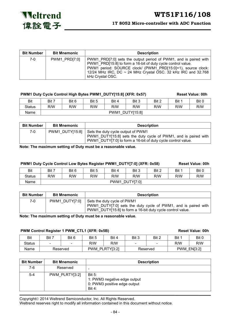
WT51F116/108 1T 8052 Micro-controller with ADC Function
Copyright 2014 Weltrend Semiconductor, Inc. All Rights Reserved. Weltrend reserves right to modify all information contained in this document without notice.
- 84 -
Bit Number Bit Mnemonic Description 7-0 PWM1_PRD[7:0] PWM1_PRD[7:0] sets the output period of PWM1, and is paired with
PWM1_PRD[15:8] to form a 16-bit of duty cycle control value. PWM1 period: SOURCE clock/ (PWM1_PRD[15:0]+1), source clock: 12/24 MHz IRC, DC ~ 24 MHz Crystal OSC. 32 kHz IRC and 32.768 kHz Crystal OSC.
PWM1 Duty Cycle Control High Bytes PWM1_DUTY[15:8] (XFR: 0x57) Reset Value: 00h
Bit Bit 7 Bit 6 Bit 5 Bit 4 Bit 3 Bit 2 Bit 1 Bit 0 Status R/W R/W R/W R/W R/W R/W R/W R/W Name PWM1_DUTY[15:8]
Bit Number Bit Mnemonic Description 7-0 PWM1_DUTY[15:8] Sets the duty cycle output of PWM1
PWM1_DUTY[15:8] sets the duty cycle of PWM1, and is paired with PWM1_DUTY[7:0] to form a 16-bit of duty cycle control value.
Note: The maximum setting of Duty must be a reasonable value.
PWM1 Duty Cycle Control Low Bytes Register PWM1_DUTY[7:0] (XFR: 0x58) Reset Value: 00h
Bit Bit 7 Bit 6 Bit 5 Bit 4 Bit 3 Bit 2 Bit 1 Bit 0 Status R/W R/W R/W R/W R/W R/W R/W R/W Name PWM1_DUTY[7:0]
Bit Number Bit Mnemonic Description 7-0 PWM1_DUTY[7:0] Sets the duty cycle of PWM1
PWM1_DUTY[7:0] sets the duty cycle of PWM1, and is paired with PWM1_DUTY[15:8] to form a 16-bit duty cycle control value.
Note: The maximum setting of Duty must be a reasonable value.
PWM Control Register 1 PWM_CTL1 (XFR: 0x5B) Reset Value: 00h
Bit Bit 7 Bit 6 Bit 5 Bit 4 Bit 3 Bit 2 Bit 1 Bit 0 Status - - R/W R/W - - R/W R/W Name Reserved PWM_PLRTY[3:2] Reserved PWM_EN[3:2]
Bit Number Bit Mnemonic Description 7-6 Reserved - 5-4 PWM_PLRTY[3:2] Bit 5:
1: PWM3 negative edge output 0: PWM3 positive edge output Bit 4:
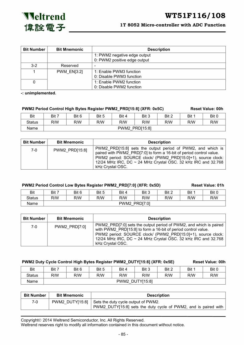
WT51F116/108 1T 8052 Micro-controller with ADC Function
Copyright 2014 Weltrend Semiconductor, Inc. All Rights Reserved. Weltrend reserves right to modify all information contained in this document without notice.
- 85 -
Bit Number Bit Mnemonic Description 1: PWM2 negative edge output 0: PWM2 positive edge output
3-2 Reserved - 1 PWM_EN[3:2] 1: Enable PWM3 function
0: Disable PWM3 function 0 1: Enable PWM2 function
0: Disable PWM2 function -: unimplemented.
PWM2 Period Control High Bytes Register PWM2_PRD[15:8] (XFR: 0x5C) Reset Value: 00h
Bit Bit 7 Bit 6 Bit 5 Bit 4 Bit 3 Bit 2 Bit 1 Bit 0 Status R/W R/W R/W R/W R/W R/W R/W R/W Name PWM2_PRD[15:8]
Bit Number Bit Mnemonic Description
7-0 PWM2_PRD[15:8] PWM2_PRD[15:8] sets the output period of PWM2, and which is paired with PWM2_PRD[7:0] to form a 16-bit of period control value. PWM2 period: SOURCE clock/ (PWM2_PRD[15:0]+1), source clock: 12/24 MHz IRC, DC ~ 24 MHz Crystal OSC. 32 kHz IRC and 32.768 kHz Crystal OSC.
PWM2 Period Control Low Bytes Register PWM2_PRD[7:0] (XFR: 0x5D) Reset Value: 01h
Bit Bit 7 Bit 6 Bit 5 Bit 4 Bit 3 Bit 2 Bit 1 Bit 0 Status R/W R/W R/W R/W R/W R/W R/W R/W Name PWM2_PRD[7:0]
Bit Number Bit Mnemonic Description
7-0 PWM2_PRD[7:0] PWM2_PRD[7:0] sets the output period of PWM2, and which is paired with PWM2_PRD[15:8] to form a 16-bit of period control value. PWM2 period: SOURCE clock/ (PWM2_PRD[15:0]+1), source clock: 12/24 MHz IRC, DC ~ 24 MHz Crystal OSC. 32 kHz IRC and 32.768 kHz Crystal OSC.
PWM2 Duty Cycle Control High Bytes Register PWM2_DUTY[15:8] (XFR: 0x5E) Reset Value: 00h
Bit Bit 7 Bit 6 Bit 5 Bit 4 Bit 3 Bit 2 Bit 1 Bit 0 Status R/W R/W R/W R/W R/W R/W R/W R/W Name PWM2_DUTY[15:8]
Bit Number Bit Mnemonic Description 7-0 PWM2_DUTY[15:8] Sets the duty cycle output of PWM2.
PWM2_DUTY[15:8] sets the duty cycle of PWM2, and is paired with
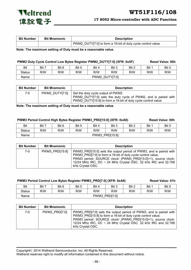
WT51F116/108 1T 8052 Micro-controller with ADC Function
Copyright 2014 Weltrend Semiconductor, Inc. All Rights Reserved. Weltrend reserves right to modify all information contained in this document without notice.
- 86 -
Bit Number Bit Mnemonic Description PWM2_DUTY[7:0] to form a 16-bit of duty cycle control value.
Note: The maximum setting of Duty must be a reasonable value.
PWM2 Duty Cycle Control Low Bytes Register PWM2_DUTY[7:0] (XFR: 0x5F) Reset Value: 00h
Bit Bit 7 Bit 6 Bit 5 Bit 4 Bit 3 Bit 2 Bit 1 Bit 0 Status R/W R/W R/W R/W R/W R/W R/W R/W Name PWM2_DUTY[7:0]
Bit Number Bit Mnemonic Description 7-0 PWM2_DUTY[7:0] Set the duty cycle output of PWM2
PWM2_DUTY[7:0] sets the duty cycle of PWM2, and is paired with PWM2_DUTY[15:8] to form a 16-bit of duty cycle control value.
Note: The maximum setting of Duty must be a reasonable value.
PWM3 Period Control High Bytes Register PWM3_PRD[15:8] (XFR: 0xA8) Reset Value: 00h
Bit Bit 7 Bit 6 Bit 5 Bit 4 Bit 3 Bit 2 Bit 1 Bit 0 Status R/W R/W R/W R/W R/W R/W R/W R/W Name PWM3_PRD[15:8]
Bit Number Bit Mnemonic Description 7-0 PWM3_PRD[15:8] PWM3_PRD[15:0] sets the output period of PWM3, and is paired with
PWM3_PRD[7:0] to form a 16-bit of duty cycle control value. PWM3 period: SOURCE clock/ (PWM3_PRD[15:0]+1), source clock: 12/24 MHz IRC, DC ~ 24 MHz Crystal OSC. 32 kHz IRC and 32.768 kHz Crystal OSC.
PWM3 Period Control Low Bytes Register PWM3_PRD[7:0] (XFR: 0xA9) Reset Value: 01h
Bit Bit 7 Bit 6 Bit 5 Bit 4 Bit 3 Bit 2 Bit 1 Bit 0 Status R/W R/W R/W R/W R/W R/W R/W R/W Name PWM3_PRD[7:0]
Bit Number Bit Mnemonic Description 7-0 PWM3_PRD[7:0] PWM3_PRD[7:0] sets the output period of PWM3, and is paired with
PWM3_PRD[15:8] to form a 16-bit of duty cycle control value. PWM3 period: SOURCE clock/ (PWM3_PRD[15:0]+1), source clock: 12/24 MHz IRC, DC ~ 24 MHz Crystal OSC. 32 kHz IRC and 32.768 kHz Crystal OSC.
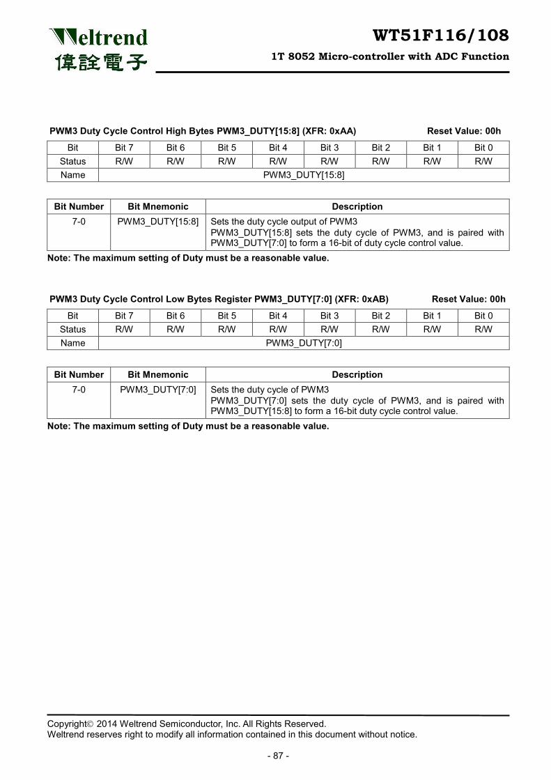
WT51F116/108 1T 8052 Micro-controller with ADC Function
Copyright 2014 Weltrend Semiconductor, Inc. All Rights Reserved. Weltrend reserves right to modify all information contained in this document without notice.
- 87 -
PWM3 Duty Cycle Control High Bytes PWM3_DUTY[15:8] (XFR: 0xAA) Reset Value: 00h
Bit Bit 7 Bit 6 Bit 5 Bit 4 Bit 3 Bit 2 Bit 1 Bit 0 Status R/W R/W R/W R/W R/W R/W R/W R/W Name PWM3_DUTY[15:8]
Bit Number Bit Mnemonic Description 7-0 PWM3_DUTY[15:8] Sets the duty cycle output of PWM3
PWM3_DUTY[15:8] sets the duty cycle of PWM3, and is paired with PWM3_DUTY[7:0] to form a 16-bit of duty cycle control value.
Note: The maximum setting of Duty must be a reasonable value.
PWM3 Duty Cycle Control Low Bytes Register PWM3_DUTY[7:0] (XFR: 0xAB) Reset Value: 00h
Bit Bit 7 Bit 6 Bit 5 Bit 4 Bit 3 Bit 2 Bit 1 Bit 0 Status R/W R/W R/W R/W R/W R/W R/W R/W Name PWM3_DUTY[7:0]
Bit Number Bit Mnemonic Description 7-0 PWM3_DUTY[7:0] Sets the duty cycle of PWM3
PWM3_DUTY[7:0] sets the duty cycle of PWM3, and is paired with PWM3_DUTY[15:8] to form a 16-bit duty cycle control value.
Note: The maximum setting of Duty must be a reasonable value.
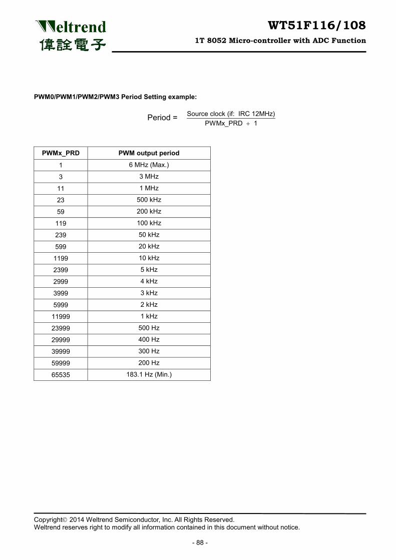
WT51F116/108 1T 8052 Micro-controller with ADC Function
Copyright 2014 Weltrend Semiconductor, Inc. All Rights Reserved. Weltrend reserves right to modify all information contained in this document without notice.
- 88 -
PWM0/PWM1/PWM2/PWM3 Period Setting example:
Period = Source clock (if: IRC 12MHz)PWMx_PRD 1+
PWMx_PRD PWM output period
1 6 MHz (Max.)
3 3 MHz
11 1 MHz
23 500 kHz
59 200 kHz
119 100 kHz
239 50 kHz
599 20 kHz
1199 10 kHz
2399 5 kHz
2999 4 kHz
3999 3 kHz
5999 2 kHz
11999 1 kHz
23999 500 Hz
29999 400 Hz
39999 300 Hz
59999 200 Hz
65535 183.1 Hz (Min.)
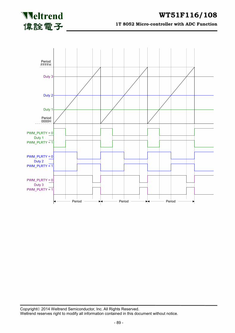
WT51F116/108 1T 8052 Micro-controller with ADC Function
Copyright 2014 Weltrend Semiconductor, Inc. All Rights Reserved. Weltrend reserves right to modify all information contained in this document without notice.
- 89 -
0000H
FFFFH
Duty 3
Duty 2
Duty 1
PWM_PLRTY = 0
PWM_PLRTY = 1
PWM_PLRTY = 0
PWM_PLRTY = 1
PWM_PLRTY = 0
PWM_PLRTY = 1
Duty 1
Duty 2
Duty 3
Period
Period
Period Period Period
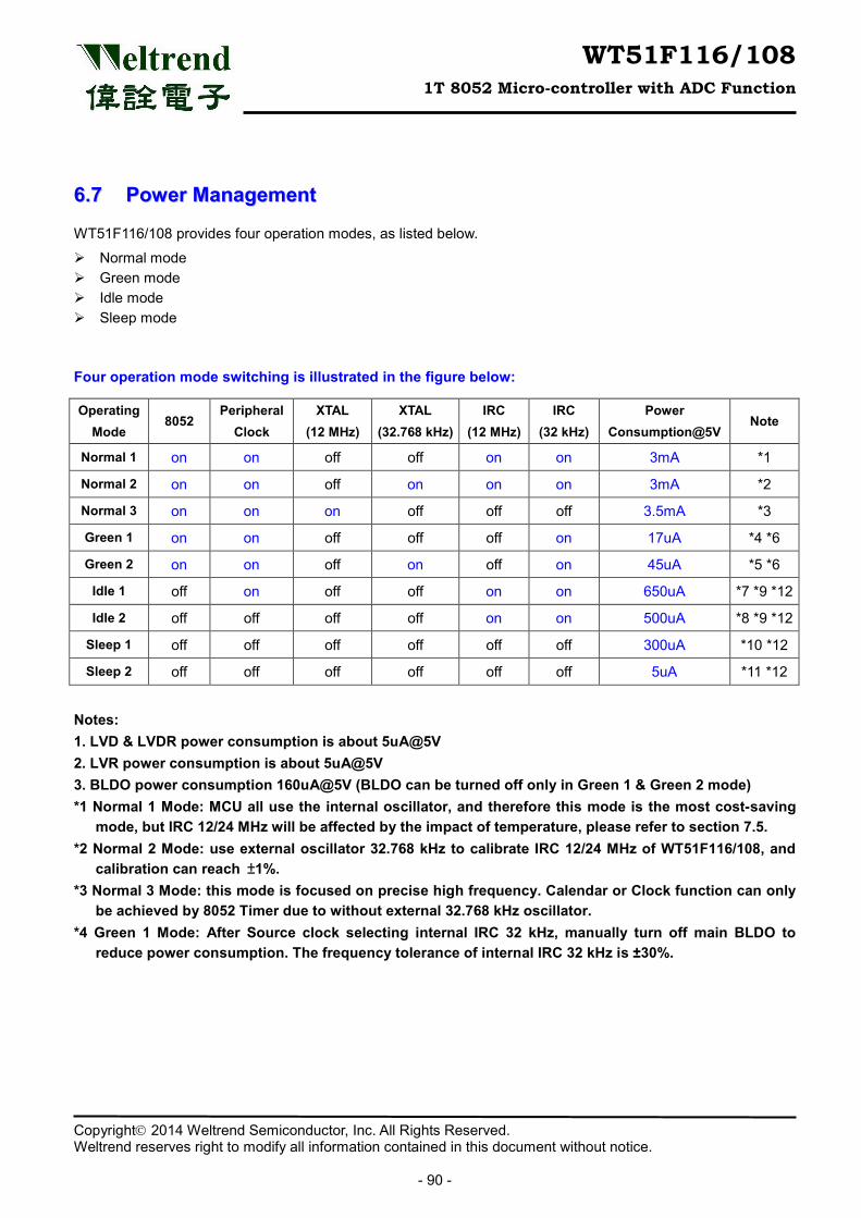
WT51F116/108 1T 8052 Micro-controller with ADC Function
Copyright 2014 Weltrend Semiconductor, Inc. All Rights Reserved. Weltrend reserves right to modify all information contained in this document without notice.
- 90 -
66..77 PPoowweerr MMaannaaggeemmeenntt
WT51F116/108 provides four operation modes, as listed below.
Normal mode Green mode Idle mode Sleep mode
Four operation mode switching is illustrated in the figure below:
Operating Mode
8052 Peripheral
Clock XTAL
(12 MHz) XTAL
(32.768 kHz) IRC
(12 MHz) IRC
(32 kHz) Power
Consumption@5V Note
Normal 1 on on off off on on 3mA *1
Normal 2 on on off on on on 3mA *2
Normal 3 on on on off off off 3.5mA *3
Green 1 on on off off off on 17uA *4 *6
Green 2 on on off on off on 45uA *5 *6
Idle 1 off on off off on on 650uA *7 *9 *12
Idle 2 off off off off on on 500uA *8 *9 *12
Sleep 1 off off off off off off 300uA *10 *12
Sleep 2 off off off off off off 5uA *11 *12
Notes: 1. LVD & LVDR power consumption is about 5uA@5V 2. LVR power consumption is about 5uA@5V 3. BLDO power consumption 160uA@5V (BLDO can be turned off only in Green 1 & Green 2 mode) *1 Normal 1 Mode: MCU all use the internal oscillator, and therefore this mode is the most cost-saving
mode, but IRC 12/24 MHz will be affected by the impact of temperature, please refer to section 7.5. *2 Normal 2 Mode: use external oscillator 32.768 kHz to calibrate IRC 12/24 MHz of WT51F116/108, and
calibration can reach ±1%. *3 Normal 3 Mode: this mode is focused on precise high frequency. Calendar or Clock function can only
be achieved by 8052 Timer due to without external 32.768 kHz oscillator. *4 Green 1 Mode: After Source clock selecting internal IRC 32 kHz, manually turn off main BLDO to
reduce power consumption. The frequency tolerance of internal IRC 32 kHz is ±30%.
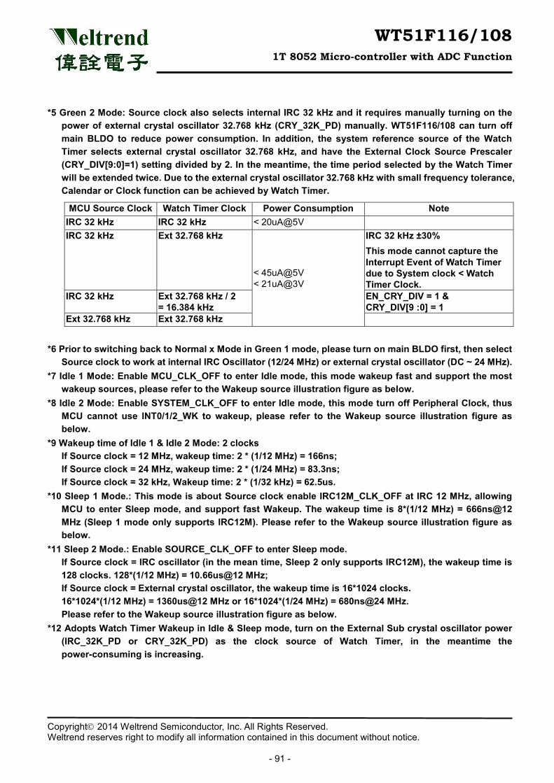
WT51F116/108 1T 8052 Micro-controller with ADC Function
Copyright 2014 Weltrend Semiconductor, Inc. All Rights Reserved. Weltrend reserves right to modify all information contained in this document without notice.
- 91 -
*5 Green 2 Mode: Source clock also selects internal IRC 32 kHz and it requires manually turning on the power of external crystal oscillator 32.768 kHz (CRY_32K_PD) manually. WT51F116/108 can turn off main BLDO to reduce power consumption. In addition, the system reference source of the Watch Timer selects external crystal oscillator 32.768 kHz, and have the External Clock Source Prescaler (CRY_DIV[9:0]=1) setting divided by 2. In the meantime, the time period selected by the Watch Timer will be extended twice. Due to the external crystal oscillator 32.768 kHz with small frequency tolerance, Calendar or Clock function can be achieved by Watch Timer.
MCU Source Clock Watch Timer Clock Power Consumption Note IRC 32 kHz IRC 32 kHz < 20uA@5V IRC 32 kHz Ext 32.768 kHz
< 45uA@5V < 21uA@3V
IRC 32 kHz ±30% This mode cannot capture the Interrupt Event of Watch Timer due to System clock < Watch Timer Clock.
IRC 32 kHz Ext 32.768 kHz / 2 = 16.384 kHz
EN_CRY_DIV = 1 & CRY_DIV[9 :0] = 1
Ext 32.768 kHz Ext 32.768 kHz
*6 Prior to switching back to Normal x Mode in Green 1 mode, please turn on main BLDO first, then select
Source clock to work at internal IRC Oscillator (12/24 MHz) or external crystal oscillator (DC ~ 24 MHz). *7 Idle 1 Mode: Enable MCU_CLK_OFF to enter Idle mode, this mode wakeup fast and support the most
wakeup sources, please refer to the Wakeup source illustration figure as below. *8 Idle 2 Mode: Enable SYSTEM_CLK_OFF to enter Idle mode, this mode turn off Peripheral Clock, thus
MCU cannot use INT0/1/2_WK to wakeup, please refer to the Wakeup source illustration figure as below.
*9 Wakeup time of Idle 1 & Idle 2 Mode: 2 clocks If Source clock = 12 MHz, wakeup time: 2 * (1/12 MHz) = 166ns; If Source clock = 24 MHz, wakeup time: 2 * (1/24 MHz) = 83.3ns; If Source clock = 32 kHz, Wakeup time: 2 * (1/32 kHz) = 62.5us.
*10 Sleep 1 Mode.: This mode is about Source clock enable IRC12M_CLK_OFF at IRC 12 MHz, allowing MCU to enter Sleep mode, and support fast Wakeup. The wakeup time is 8*(1/12 MHz) = 666ns@12 MHz (Sleep 1 mode only supports IRC12M). Please refer to the Wakeup source illustration figure as below.
*11 Sleep 2 Mode.: Enable SOURCE_CLK_OFF to enter Sleep mode. If Source clock = IRC oscillator (in the mean time, Sleep 2 only supports IRC12M), the wakeup time is 128 clocks. 128*(1/12 MHz) = 10.66us@12 MHz; If Source clock = External crystal oscillator, the wakeup time is 16*1024 clocks. 16*1024*(1/12 MHz) = 1360us@12 MHz or 16*1024*(1/24 MHz) = 680ns@24 MHz. Please refer to the Wakeup source illustration figure as below.
*12 Adopts Watch Timer Wakeup in Idle & Sleep mode, turn on the External Sub crystal oscillator power (IRC_32K_PD or CRY_32K_PD) as the clock source of Watch Timer, in the meantime the power-consuming is increasing.
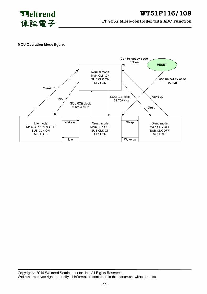
WT51F116/108 1T 8052 Micro-controller with ADC Function
Copyright 2014 Weltrend Semiconductor, Inc. All Rights Reserved. Weltrend reserves right to modify all information contained in this document without notice.
- 92 -
MCU Operation Mode figure:
Normal modeMain CLK ONSUB CLK ON
MCU ON
RESET
Green modeMain CLK OFFSUB CLK ON
MCU ON
Sleep modeMain CLK OFFSUB CLK OFF
MCU OFF
Idle modeMain CLK ON or OFF
SUB CLK ONMCU OFF
Wake up
Wake up
SOURCE clock= 12/24 MHz
SOURCE clock= 32.768 kHz
Can be set by code option
Sleep
Sleep
Wake upIdle
Wake up
Idle
Can be set by code option
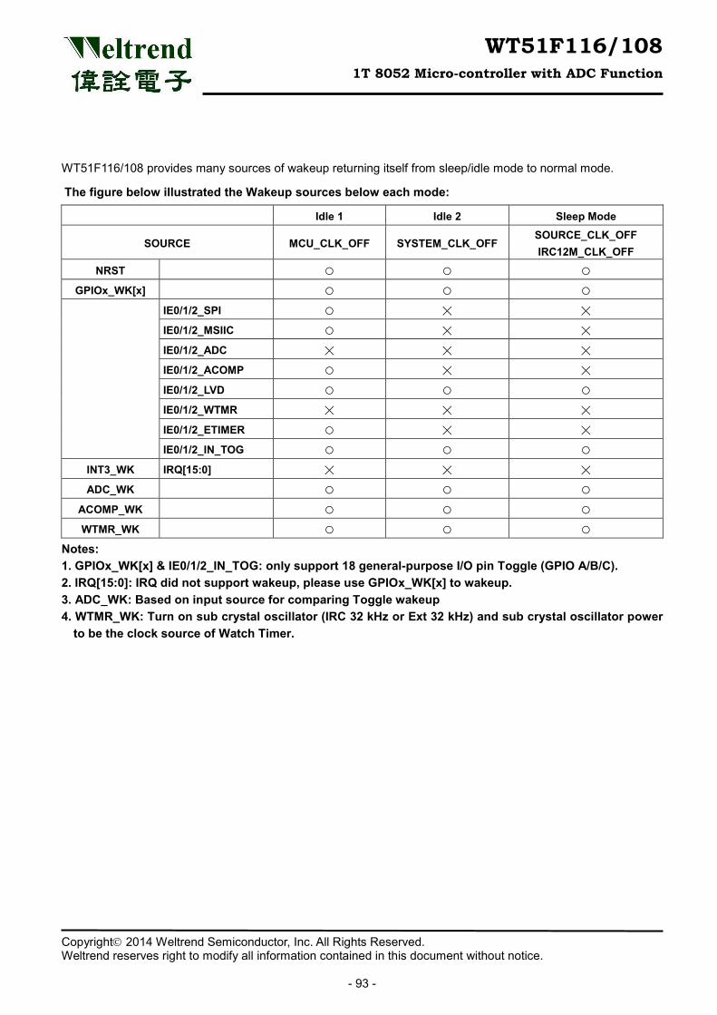
WT51F116/108 1T 8052 Micro-controller with ADC Function
Copyright 2014 Weltrend Semiconductor, Inc. All Rights Reserved. Weltrend reserves right to modify all information contained in this document without notice.
- 93 -
WT51F116/108 provides many sources of wakeup returning itself from sleep/idle mode to normal mode.
The figure below illustrated the Wakeup sources below each mode:
Idle 1 Idle 2 Sleep Mode
SOURCE MCU_CLK_OFF SYSTEM_CLK_OFF SOURCE_CLK_OFF IRC12M_CLK_OFF
NRST ○ ○ ○
GPIOx_WK[x] ○ ○ ○
IE0/1/2_SPI ○ ╳ ╳
IE0/1/2_MSIIC ○ ╳ ╳
IE0/1/2_ADC ╳ ╳ ╳
IE0/1/2_ACOMP ○ ╳ ╳
IE0/1/2_LVD ○ ○ ○
IE0/1/2_WTMR ╳ ╳ ╳
IE0/1/2_ETIMER ○ ╳ ╳
IE0/1/2_IN_TOG ○ ○ ○
INT3_WK IRQ[15:0] ╳ ╳ ╳
ADC_WK ○ ○ ○
ACOMP_WK ○ ○ ○
WTMR_WK ○ ○ ○
Notes: 1. GPIOx_WK[x] & IE0/1/2_IN_TOG: only support 18 general-purpose I/O pin Toggle (GPIO A/B/C). 2. IRQ[15:0]: IRQ did not support wakeup, please use GPIOx_WK[x] to wakeup. 3. ADC_WK: Based on input source for comparing Toggle wakeup 4. WTMR_WK: Turn on sub crystal oscillator (IRC 32 kHz or Ext 32 kHz) and sub crystal oscillator power
to be the clock source of Watch Timer.
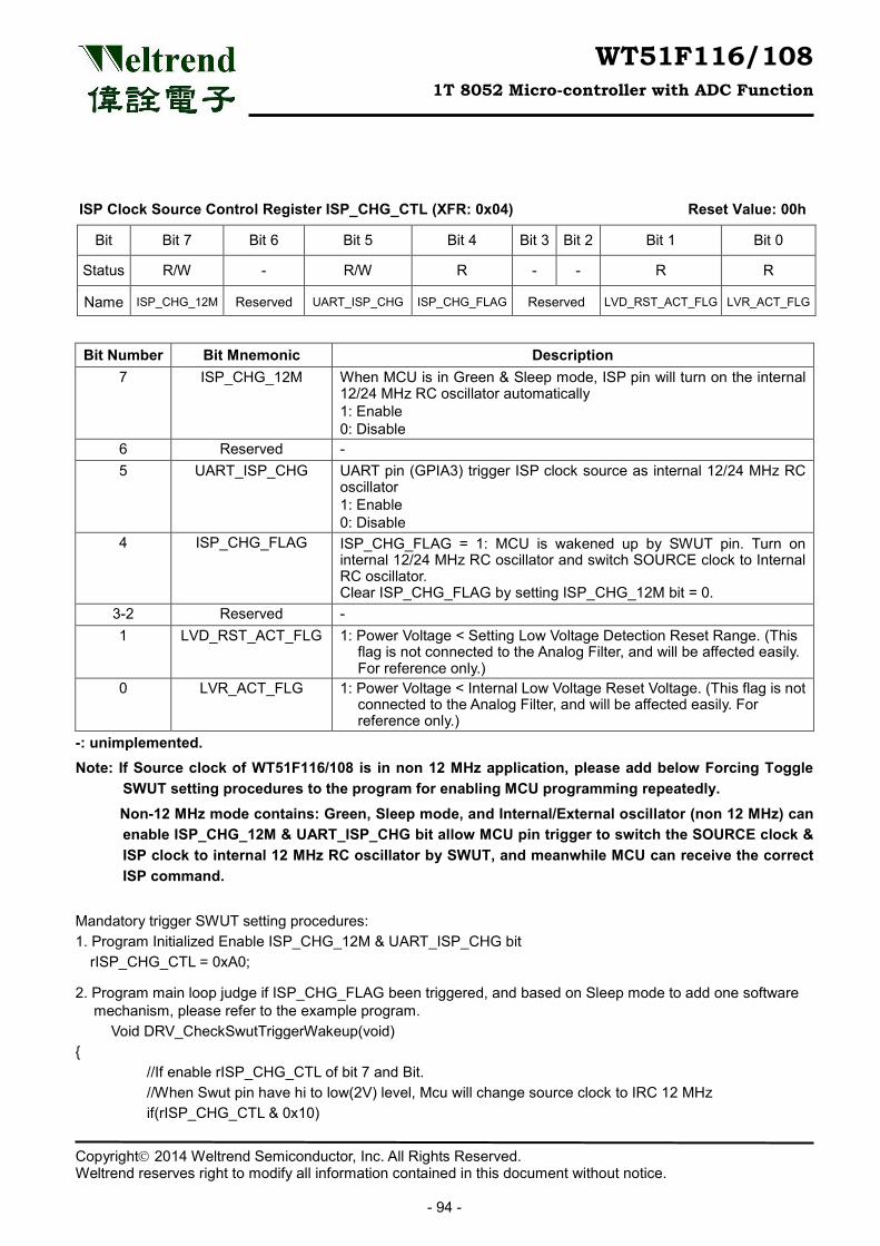
WT51F116/108 1T 8052 Micro-controller with ADC Function
Copyright 2014 Weltrend Semiconductor, Inc. All Rights Reserved. Weltrend reserves right to modify all information contained in this document without notice.
- 94 -
ISP Clock Source Control Register ISP_CHG_CTL (XFR: 0x04) Reset Value: 00h
Bit Bit 7 Bit 6 Bit 5 Bit 4 Bit 3 Bit 2 Bit 1 Bit 0
Status R/W - R/W R - - R R
Name ISP_CHG_12M Reserved UART_ISP_CHG ISP_CHG_FLAG Reserved LVD_RST_ACT_FLG LVR_ACT_FLG
Bit Number Bit Mnemonic Description 7 ISP_CHG_12M When MCU is in Green & Sleep mode, ISP pin will turn on the internal
12/24 MHz RC oscillator automatically 1: Enable 0: Disable
6 Reserved - 5 UART_ISP_CHG UART pin (GPIA3) trigger ISP clock source as internal 12/24 MHz RC
oscillator 1: Enable 0: Disable
4 ISP_CHG_FLAG ISP_CHG_FLAG = 1: MCU is wakened up by SWUT pin. Turn on internal 12/24 MHz RC oscillator and switch SOURCE clock to Internal RC oscillator. Clear ISP_CHG_FLAG by setting ISP_CHG_12M bit = 0.
3-2 Reserved - 1 LVD_RST_ACT_FLG 1: Power Voltage < Setting Low Voltage Detection Reset Range. (This
flag is not connected to the Analog Filter, and will be affected easily. For reference only.)
0 LVR_ACT_FLG 1: Power Voltage < Internal Low Voltage Reset Voltage. (This flag is not connected to the Analog Filter, and will be affected easily. For reference only.)
-: unimplemented. Note: If Source clock of WT51F116/108 is in non 12 MHz application, please add below Forcing Toggle
SWUT setting procedures to the program for enabling MCU programming repeatedly. Non-12 MHz mode contains: Green, Sleep mode, and Internal/External oscillator (non 12 MHz) can enable ISP_CHG_12M & UART_ISP_CHG bit allow MCU pin trigger to switch the SOURCE clock & ISP clock to internal 12 MHz RC oscillator by SWUT, and meanwhile MCU can receive the correct ISP command.
Mandatory trigger SWUT setting procedures: 1. Program Initialized Enable ISP_CHG_12M & UART_ISP_CHG bit
rISP_CHG_CTL = 0xA0;
2. Program main loop judge if ISP_CHG_FLAG been triggered, and based on Sleep mode to add one software mechanism, please refer to the example program.
Void DRV_CheckSwutTriggerWakeup(void) { //If enable rISP_CHG_CTL of bit 7 and Bit. //When Swut pin have hi to low(2V) level, Mcu will change source clock to IRC 12 MHz if(rISP_CHG_CTL & 0x10)
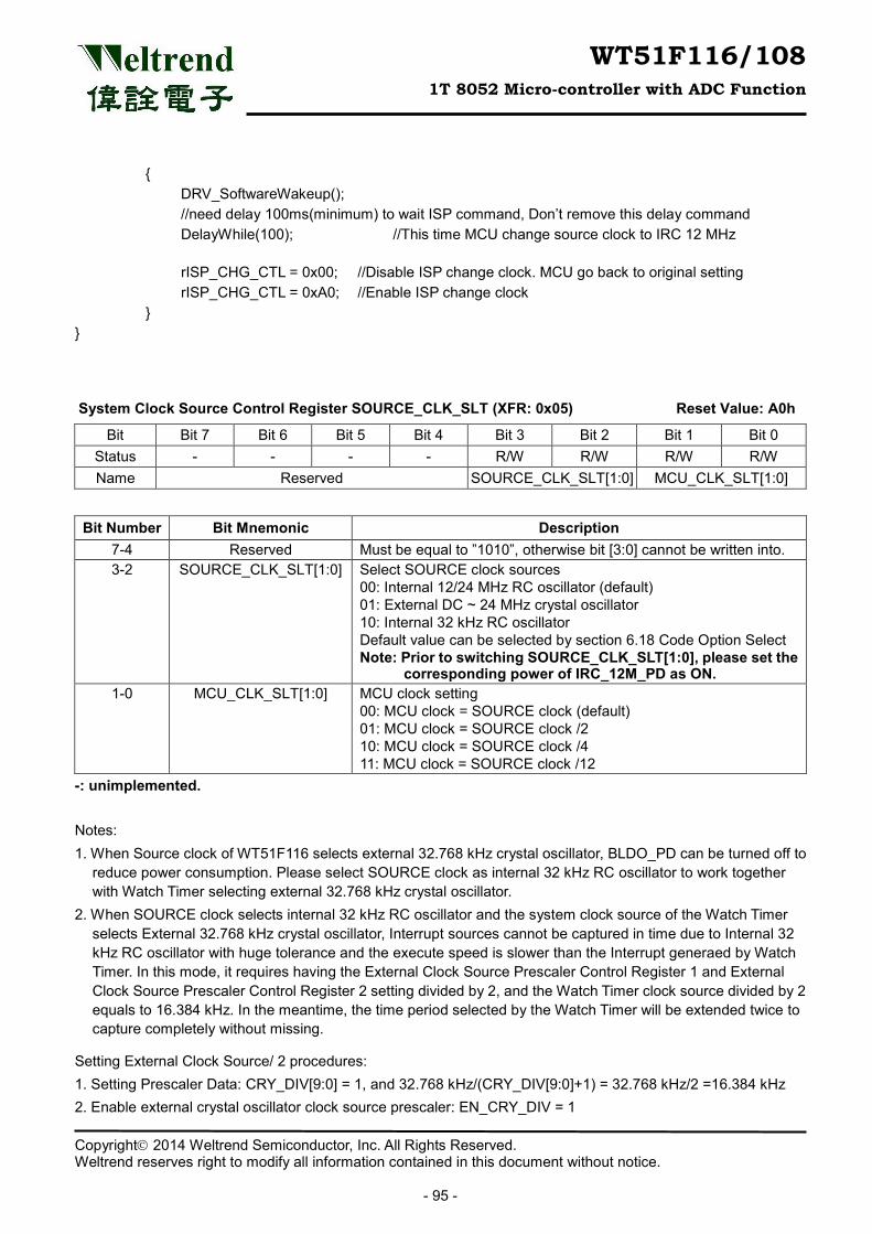
WT51F116/108 1T 8052 Micro-controller with ADC Function
Copyright 2014 Weltrend Semiconductor, Inc. All Rights Reserved. Weltrend reserves right to modify all information contained in this document without notice.
- 95 -
{ DRV_SoftwareWakeup(); //need delay 100ms(minimum) to wait ISP command, Don’t remove this delay command DelayWhile(100); //This time MCU change source clock to IRC 12 MHz rISP_CHG_CTL = 0x00; //Disable ISP change clock. MCU go back to original setting rISP_CHG_CTL = 0xA0; //Enable ISP change clock } }
System Clock Source Control Register SOURCE_CLK_SLT (XFR: 0x05) Reset Value: A0h
Bit Bit 7 Bit 6 Bit 5 Bit 4 Bit 3 Bit 2 Bit 1 Bit 0 Status - - - - R/W R/W R/W R/W Name Reserved SOURCE_CLK_SLT[1:0] MCU_CLK_SLT[1:0]
Bit Number Bit Mnemonic Description 7-4 Reserved Must be equal to ”1010”, otherwise bit [3:0] cannot be written into. 3-2 SOURCE_CLK_SLT[1:0] Select SOURCE clock sources
00: Internal 12/24 MHz RC oscillator (default) 01: External DC ~ 24 MHz crystal oscillator 10: Internal 32 kHz RC oscillator Default value can be selected by section 6.18 Code Option Select Note: Prior to switching SOURCE_CLK_SLT[1:0], please set the
corresponding power of IRC_12M_PD as ON. 1-0 MCU_CLK_SLT[1:0] MCU clock setting
00: MCU clock = SOURCE clock (default) 01: MCU clock = SOURCE clock /2 10: MCU clock = SOURCE clock /4 11: MCU clock = SOURCE clock /12
-: unimplemented. Notes: 1. When Source clock of WT51F116 selects external 32.768 kHz crystal oscillator, BLDO_PD can be turned off to
reduce power consumption. Please select SOURCE clock as internal 32 kHz RC oscillator to work together with Watch Timer selecting external 32.768 kHz crystal oscillator.
2. When SOURCE clock selects internal 32 kHz RC oscillator and the system clock source of the Watch Timer selects External 32.768 kHz crystal oscillator, Interrupt sources cannot be captured in time due to Internal 32 kHz RC oscillator with huge tolerance and the execute speed is slower than the Interrupt generaed by Watch Timer. In this mode, it requires having the External Clock Source Prescaler Control Register 1 and External Clock Source Prescaler Control Register 2 setting divided by 2, and the Watch Timer clock source divided by 2 equals to 16.384 kHz. In the meantime, the time period selected by the Watch Timer will be extended twice to capture completely without missing.
Setting External Clock Source/ 2 procedures: 1. Setting Prescaler Data: CRY_DIV[9:0] = 1, and 32.768 kHz/(CRY_DIV[9:0]+1) = 32.768 kHz/2 =16.384 kHz 2. Enable external crystal oscillator clock source prescaler: EN_CRY_DIV = 1
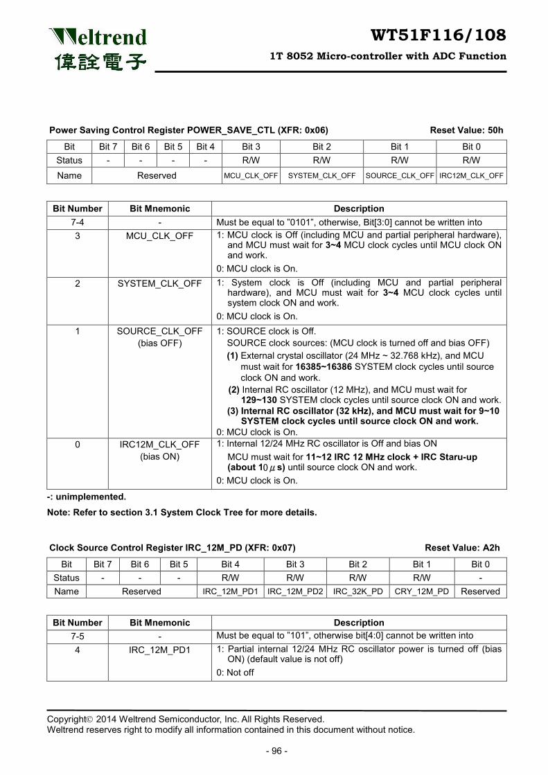
WT51F116/108 1T 8052 Micro-controller with ADC Function
Copyright 2014 Weltrend Semiconductor, Inc. All Rights Reserved. Weltrend reserves right to modify all information contained in this document without notice.
- 96 -
Power Saving Control Register POWER_SAVE_CTL (XFR: 0x06) Reset Value: 50h
Bit Bit 7 Bit 6 Bit 5 Bit 4 Bit 3 Bit 2 Bit 1 Bit 0 Status - - - - R/W R/W R/W R/W Name Reserved MCU_CLK_OFF SYSTEM_CLK_OFF SOURCE_CLK_OFF IRC12M_CLK_OFF
Bit Number Bit Mnemonic Description 7-4 - Must be equal to ”0101”, otherwise, Bit[3:0] cannot be written into 3 MCU_CLK_OFF 1: MCU clock is Off (including MCU and partial peripheral hardware),
and MCU must wait for 3~4 MCU clock cycles until MCU clock ON and work.
0: MCU clock is On. 2 SYSTEM_CLK_OFF 1: System clock is Off (including MCU and partial peripheral
hardware), and MCU must wait for 3~4 MCU clock cycles until system clock ON and work.
0: MCU clock is On. 1 SOURCE_CLK_OFF
(bias OFF) 1: SOURCE clock is Off.
SOURCE clock sources: (MCU clock is turned off and bias OFF) (1) External crystal oscillator (24 MHz ~ 32.768 kHz), and MCU
must wait for 16385~16386 SYSTEM clock cycles until source clock ON and work.
(2) Internal RC oscillator (12 MHz), and MCU must wait for 129~130 SYSTEM clock cycles until source clock ON and work.
(3) Internal RC oscillator (32 kHz), and MCU must wait for 9~10 SYSTEM clock cycles until source clock ON and work.
0: MCU clock is On. 0 IRC12M_CLK_OFF
(bias ON) 1: Internal 12/24 MHz RC oscillator is Off and bias ON
MCU must wait for 11~12 IRC 12 MHz clock + IRC Staru-up (about 10μs) until source clock ON and work.
0: MCU clock is On.
-: unimplemented. Note: Refer to section 3.1 System Clock Tree for more details.
Clock Source Control Register IRC_12M_PD (XFR: 0x07) Reset Value: A2h
Bit Bit 7 Bit 6 Bit 5 Bit 4 Bit 3 Bit 2 Bit 1 Bit 0 Status - - - R/W R/W R/W R/W - Name Reserved IRC_12M_PD1 IRC_12M_PD2 IRC_32K_PD CRY_12M_PD Reserved
Bit Number Bit Mnemonic Description 7-5 - Must be equal to ”101”, otherwise bit[4:0] cannot be written into 4 IRC_12M_PD1 1: Partial internal 12/24 MHz RC oscillator power is turned off (bias
ON) (default value is not off) 0: Not off
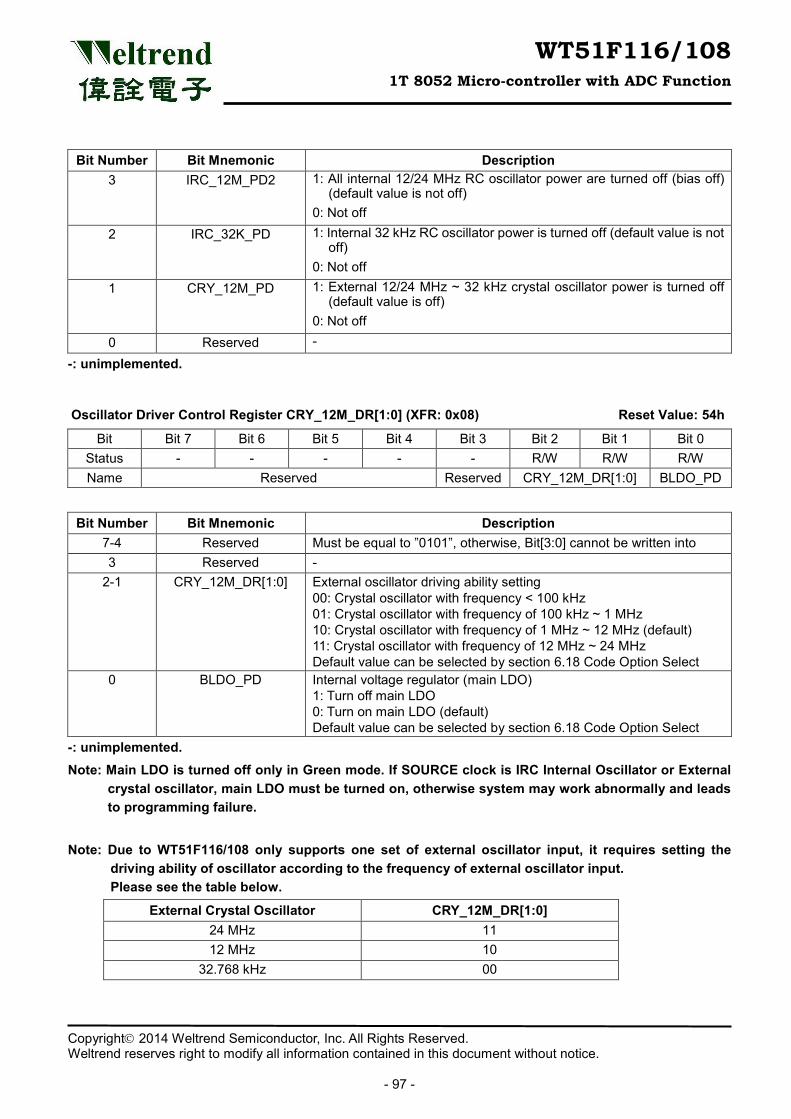
WT51F116/108 1T 8052 Micro-controller with ADC Function
Copyright 2014 Weltrend Semiconductor, Inc. All Rights Reserved. Weltrend reserves right to modify all information contained in this document without notice.
- 97 -
Bit Number Bit Mnemonic Description 3 IRC_12M_PD2 1: All internal 12/24 MHz RC oscillator power are turned off (bias off)
(default value is not off) 0: Not off
2 IRC_32K_PD 1: Internal 32 kHz RC oscillator power is turned off (default value is not off)
0: Not off 1 CRY_12M_PD 1: External 12/24 MHz ~ 32 kHz crystal oscillator power is turned off
(default value is off) 0: Not off
0 Reserved -
-: unimplemented.
Oscillator Driver Control Register CRY_12M_DR[1:0] (XFR: 0x08) Reset Value: 54h
Bit Bit 7 Bit 6 Bit 5 Bit 4 Bit 3 Bit 2 Bit 1 Bit 0 Status - - - - - R/W R/W R/W Name Reserved Reserved CRY_12M_DR[1:0] BLDO_PD
Bit Number Bit Mnemonic Description 7-4 Reserved Must be equal to ”0101”, otherwise, Bit[3:0] cannot be written into 3 Reserved -
2-1 CRY_12M_DR[1:0] External oscillator driving ability setting 00: Crystal oscillator with frequency < 100 kHz 01: Crystal oscillator with frequency of 100 kHz ~ 1 MHz 10: Crystal oscillator with frequency of 1 MHz ~ 12 MHz (default) 11: Crystal oscillator with frequency of 12 MHz ~ 24 MHz Default value can be selected by section 6.18 Code Option Select
0 BLDO_PD Internal voltage regulator (main LDO) 1: Turn off main LDO 0: Turn on main LDO (default) Default value can be selected by section 6.18 Code Option Select
-: unimplemented. Note: Main LDO is turned off only in Green mode. If SOURCE clock is IRC Internal Oscillator or External
crystal oscillator, main LDO must be turned on, otherwise system may work abnormally and leads to programming failure.
Note: Due to WT51F116/108 only supports one set of external oscillator input, it requires setting the
driving ability of oscillator according to the frequency of external oscillator input. Please see the table below.
External Crystal Oscillator CRY_12M_DR[1:0] 24 MHz 11 12 MHz 10
32.768 kHz 00
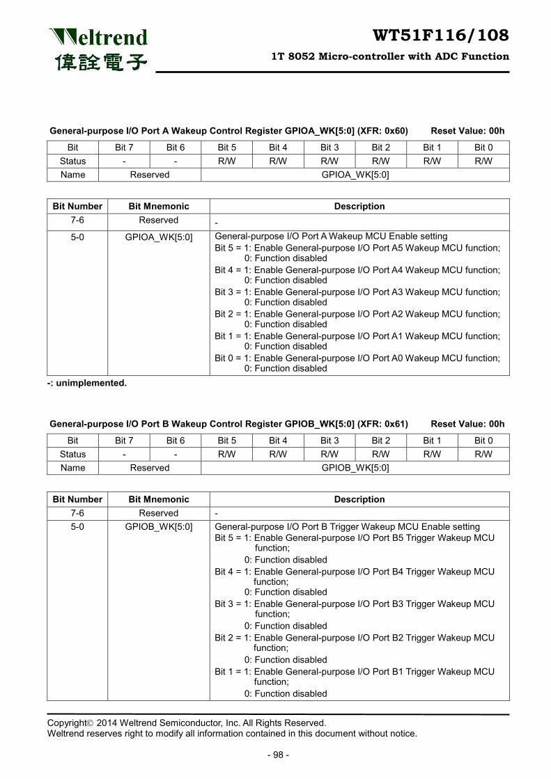
WT51F116/108 1T 8052 Micro-controller with ADC Function
Copyright 2014 Weltrend Semiconductor, Inc. All Rights Reserved. Weltrend reserves right to modify all information contained in this document without notice.
- 98 -
General-purpose I/O Port A Wakeup Control Register GPIOA_WK[5:0] (XFR: 0x60) Reset Value: 00h
Bit Bit 7 Bit 6 Bit 5 Bit 4 Bit 3 Bit 2 Bit 1 Bit 0 Status - - R/W R/W R/W R/W R/W R/W Name Reserved GPIOA_WK[5:0]
Bit Number Bit Mnemonic Description 7-6 Reserved - 5-0 GPIOA_WK[5:0] General-purpose I/O Port A Wakeup MCU Enable setting
Bit 5 = 1: Enable General-purpose I/O Port A5 Wakeup MCU function; 0: Function disabled
Bit 4 = 1: Enable General-purpose I/O Port A4 Wakeup MCU function; 0: Function disabled
Bit 3 = 1: Enable General-purpose I/O Port A3 Wakeup MCU function; 0: Function disabled
Bit 2 = 1: Enable General-purpose I/O Port A2 Wakeup MCU function; 0: Function disabled
Bit 1 = 1: Enable General-purpose I/O Port A1 Wakeup MCU function; 0: Function disabled
Bit 0 = 1: Enable General-purpose I/O Port A0 Wakeup MCU function; 0: Function disabled
-: unimplemented.
General-purpose I/O Port B Wakeup Control Register GPIOB_WK[5:0] (XFR: 0x61) Reset Value: 00h
Bit Bit 7 Bit 6 Bit 5 Bit 4 Bit 3 Bit 2 Bit 1 Bit 0 Status - - R/W R/W R/W R/W R/W R/W Name Reserved GPIOB_WK[5:0]
Bit Number Bit Mnemonic Description 7-6 Reserved - 5-0 GPIOB_WK[5:0]
General-purpose I/O Port B Trigger Wakeup MCU Enable setting Bit 5 = 1: Enable General-purpose I/O Port B5 Trigger Wakeup MCU
function; 0: Function disabled
Bit 4 = 1: Enable General-purpose I/O Port B4 Trigger Wakeup MCU function; 0: Function disabled
Bit 3 = 1: Enable General-purpose I/O Port B3 Trigger Wakeup MCU function;
0: Function disabled Bit 2 = 1: Enable General-purpose I/O Port B2 Trigger Wakeup MCU
function; 0: Function disabled
Bit 1 = 1: Enable General-purpose I/O Port B1 Trigger Wakeup MCU function;
0: Function disabled
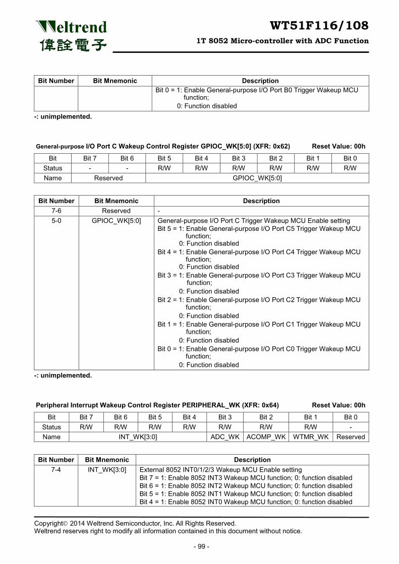
WT51F116/108 1T 8052 Micro-controller with ADC Function
Copyright 2014 Weltrend Semiconductor, Inc. All Rights Reserved. Weltrend reserves right to modify all information contained in this document without notice.
- 99 -
Bit Number Bit Mnemonic Description Bit 0 = 1: Enable General-purpose I/O Port B0 Trigger Wakeup MCU
function; 0: Function disabled
-: unimplemented.
General-purpose I/O Port C Wakeup Control Register GPIOC_WK[5:0] (XFR: 0x62) Reset Value: 00h
Bit Bit 7 Bit 6 Bit 5 Bit 4 Bit 3 Bit 2 Bit 1 Bit 0 Status - - R/W R/W R/W R/W R/W R/W Name Reserved GPIOC_WK[5:0]
Bit Number Bit Mnemonic Description 7-6 Reserved - 5-0 GPIOC_WK[5:0] General-purpose I/O Port C Trigger Wakeup MCU Enable setting
Bit 5 = 1: Enable General-purpose I/O Port C5 Trigger Wakeup MCU function; 0: Function disabled
Bit 4 = 1: Enable General-purpose I/O Port C4 Trigger Wakeup MCU function; 0: Function disabled
Bit 3 = 1: Enable General-purpose I/O Port C3 Trigger Wakeup MCU function;
0: Function disabled Bit 2 = 1: Enable General-purpose I/O Port C2 Trigger Wakeup MCU
function; 0: Function disabled
Bit 1 = 1: Enable General-purpose I/O Port C1 Trigger Wakeup MCU function;
0: Function disabled Bit 0 = 1: Enable General-purpose I/O Port C0 Trigger Wakeup MCU
function; 0: Function disabled
-: unimplemented.
Peripheral Interrupt Wakeup Control Register PERIPHERAL_WK (XFR: 0x64) Reset Value: 00h
Bit Bit 7 Bit 6 Bit 5 Bit 4 Bit 3 Bit 2 Bit 1 Bit 0 Status R/W R/W R/W R/W R/W R/W R/W - Name INT_WK[3:0] ADC_WK ACOMP_WK WTMR_WK Reserved
Bit Number Bit Mnemonic Description 7-4 INT_WK[3:0] External 8052 INT0/1/2/3 Wakeup MCU Enable setting
Bit 7 = 1: Enable 8052 INT3 Wakeup MCU function; 0: function disabled Bit 6 = 1: Enable 8052 INT2 Wakeup MCU function; 0: function disabled Bit 5 = 1: Enable 8052 INT1 Wakeup MCU function; 0: function disabled Bit 4 = 1: Enable 8052 INT0 Wakeup MCU function; 0: function disabled
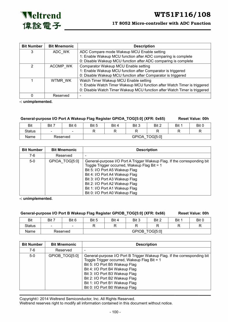
WT51F116/108 1T 8052 Micro-controller with ADC Function
Copyright 2014 Weltrend Semiconductor, Inc. All Rights Reserved. Weltrend reserves right to modify all information contained in this document without notice.
- 100 -
Bit Number Bit Mnemonic Description 3 ADC_WK ADC Compare mode Wakeup MCU Enable setting
1: Enable Wakeup MCU function after ADC comparing is complete 0: Disable Wakeup MCU function after ADC comparing is complete
2 ACOMP_WK Comparator Wakeup MCU Enable setting 1: Enable Wakeup MCU function after Comparator is triggered 0: Disable Wakeup MCU function after Comparator is triggered
1 WTMR_WK Watch Timer Wakeup MCU Enable setting 1: Enable Watch Timer Wakeup MCU function after Watch Timer is triggered 0: Disable Watch Timer Wakeup MCU function after Watch Timer is triggered
0 Reserved - -: unimplemented.
General-purpose I/O Port A Wakeup Flag Register GPIOA_TOG[5:0] (XFR: 0x65) Reset Value: 00h
Bit Bit 7 Bit 6 Bit 5 Bit 4 Bit 3 Bit 2 Bit 1 Bit 0 Status - - R R R R R R Name Reserved GPIOA_TOG[5:0]
Bit Number Bit Mnemonic Description 7-6 Reserved - 5-0 GPIOA_TOG[5:0] General-purpose I/O Port A Trigger Wakeup Flag. If the corresponding bit
Toggle Trigger occurred, Wakeup Flag Bit = 1 Bit 5: I/O Port A5 Wakeup Flag Bit 4: I/O Port A4 Wakeup Flag Bit 3: I/O Port A3 Wakeup Flag Bit 2: I/O Port A2 Wakeup Flag Bit 1: I/O Port A1 Wakeup Flag Bit 0: I/O Port A0 Wakeup Flag
-: unimplemented.
General-purpose I/O Port B Wakeup Flag Register GPIOB_TOG[5:0] (XFR: 0x66) Reset Value: 00h
Bit Bit 7 Bit 6 Bit 5 Bit 4 Bit 3 Bit 2 Bit 1 Bit 0 Status - - R R R R R R Name Reserved GPIOB_TOG[5:0]
Bit Number Bit Mnemonic Description 7-6 Reserved - 5-0 GPIOB_TOG[5:0] General-purpose I/O Port B Trigger Wakeup Flag. If the corresponding bit
Toggle Trigger occurred, Wakeup Flag Bit = 1 Bit 5: I/O Port B5 Wakeup Flag Bit 4: I/O Port B4 Wakeup Flag Bit 3: I/O Port B3 Wakeup Flag Bit 2: I/O Port B2 Wakeup Flag Bit 1: I/O Port B1 Wakeup Flag Bit 0: I/O Port B0 Wakeup Flag
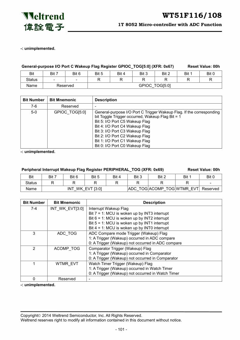
WT51F116/108 1T 8052 Micro-controller with ADC Function
Copyright 2014 Weltrend Semiconductor, Inc. All Rights Reserved. Weltrend reserves right to modify all information contained in this document without notice.
- 101 -
-: unimplemented.
General-purpose I/O Port C Wakeup Flag Register GPIOC_TOG[5:0] (XFR: 0x67) Reset Value: 00h
Bit Bit 7 Bit 6 Bit 5 Bit 4 Bit 3 Bit 2 Bit 1 Bit 0 Status - - R R R R R R Name Reserved GPIOC_TOG[5:0]
Bit Number Bit Mnemonic Description 7-6 Reserved - 5-0 GPIOC_TOG[5:0] General-purpose I/O Port C Trigger Wakeup Flag. If the corresponding
bit Toggle Trigger occurred, Wakeup Flag Bit = 1 Bit 5: I/O Port C5 Wakeup Flag Bit 4: I/O Port C4 Wakeup Flag Bit 3: I/O Port C3 Wakeup Flag Bit 2: I/O Port C2 Wakeup Flag Bit 1: I/O Port C1 Wakeup Flag Bit 0: I/O Port C0 Wakeup Flag
-: unimplemented.
Peripheral Interrupt Wakeup Flag Register PERIPHERAL_TOG (XFR: 0x69) Reset Value: 00h
Bit Bit 7 Bit 6 Bit 5 Bit 4 Bit 3 Bit 2 Bit 1 Bit 0 Status R R R R R R R - Name INT_WK_EVT [3:0] ADC_TOG ACOMP_TOG WTMR_EVT Reserved
Bit Number Bit Mnemonic Description 7-4 INT_WK_EVT[3:0] Interrupt Wakeup Flag
Bit 7 = 1: MCU is woken up by INT3 interrupt Bit 6 = 1: MCU is woken up by INT2 interrupt Bit 5 = 1: MCU is woken up by INT1 interrupt Bit 4 = 1: MCU is woken up by INT0 interrupt
3 ADC_TOG ADC Compare mode Trigger (Wakeup) Flag 1: A Trigger (Wakeup) occurred in ADC compare 0: A Trigger (Wakeup) not occurred in ADC compare
2 ACOMP_TOG Comparator Trigger (Wakeup) Flag 1: A Trigger (Wakeup) occurred in Comparator 0: A Trigger (Wakeup) not occurred in Comparator
1 WTMR_EVT Watch Timer Trigger (Wakeup) Flag 1: A Trigger (Wakeup) occurred in Watch Timer 0: A Trigger (Wakeup) not occurred in Watch Timer
0 Reserved - -: unimplemented.
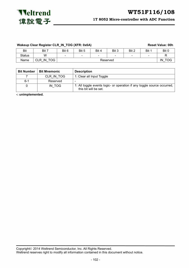
WT51F116/108 1T 8052 Micro-controller with ADC Function
Copyright 2014 Weltrend Semiconductor, Inc. All Rights Reserved. Weltrend reserves right to modify all information contained in this document without notice.
- 102 -
Wakeup Clear Register CLR_IN_TOG (XFR: 0x6A) Reset Value: 00h
Bit Bit 7 Bit 6 Bit 5 Bit 4 Bit 3 Bit 2 Bit 1 Bit 0 Status W - - - - - - R Name CLR_IN_TOG Reserved IN_TOG
Bit Number Bit Mnemonic Description 7 CLR_IN_TOG 1: Clear all Input Toggle
6-1 Reserved - 0 IN_TOG 1: All toggle events logic- or operation if any toggle source occurred,
this bit will be set.
-: unimplemented.
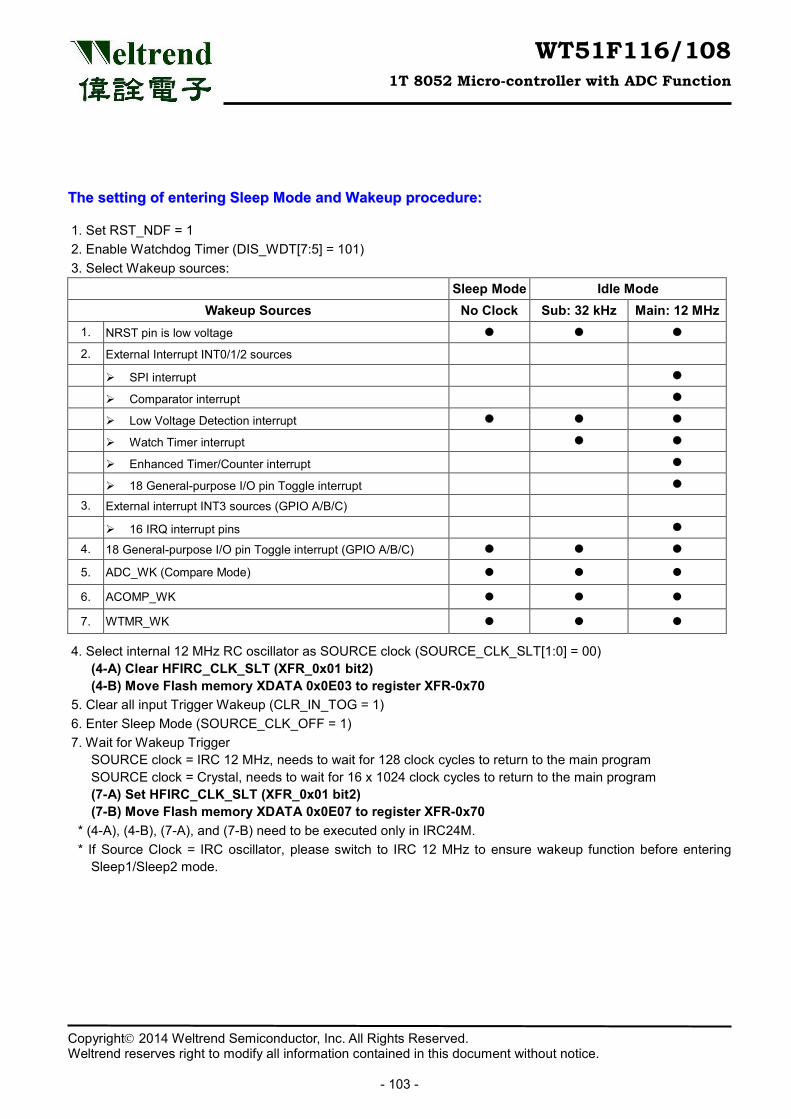
WT51F116/108 1T 8052 Micro-controller with ADC Function
Copyright 2014 Weltrend Semiconductor, Inc. All Rights Reserved. Weltrend reserves right to modify all information contained in this document without notice.
- 103 -
TThhee sseettttiinngg ooff eenntteerriinngg SSlleeeepp MMooddee aanndd WWaakkeeuupp pprroocceedduurree::
1. Set RST_NDF = 1 2. Enable Watchdog Timer (DIS_WDT[7:5] = 101) 3. Select Wakeup sources:
Sleep Mode Idle Mode Wakeup Sources No Clock Sub: 32 kHz Main: 12 MHz
1. NRST pin is low voltage ● ● ●
2. External Interrupt INT0/1/2 sources
SPI interrupt ●
Comparator interrupt ●
Low Voltage Detection interrupt ● ● ●
Watch Timer interrupt ● ●
Enhanced Timer/Counter interrupt ●
18 General-purpose I/O pin Toggle interrupt ●
3. External interrupt INT3 sources (GPIO A/B/C)
16 IRQ interrupt pins ●
4. 18 General-purpose I/O pin Toggle interrupt (GPIO A/B/C) ● ● ●
5. ADC_WK (Compare Mode) ● ● ●
6. ACOMP_WK ● ● ●
7. WTMR_WK ● ● ●
4. Select internal 12 MHz RC oscillator as SOURCE clock (SOURCE_CLK_SLT[1:0] = 00) (4-A) Clear HFIRC_CLK_SLT (XFR_0x01 bit2) (4-B) Move Flash memory XDATA 0x0E03 to register XFR-0x70
5. Clear all input Trigger Wakeup (CLR_IN_TOG = 1) 6. Enter Sleep Mode (SOURCE_CLK_OFF = 1) 7. Wait for Wakeup Trigger
SOURCE clock = IRC 12 MHz, needs to wait for 128 clock cycles to return to the main program SOURCE clock = Crystal, needs to wait for 16 x 1024 clock cycles to return to the main program (7-A) Set HFIRC_CLK_SLT (XFR_0x01 bit2) (7-B) Move Flash memory XDATA 0x0E07 to register XFR-0x70
* (4-A), (4-B), (7-A), and (7-B) need to be executed only in IRC24M. * If Source Clock = IRC oscillator, please switch to IRC 12 MHz to ensure wakeup function before entering
Sleep1/Sleep2 mode.
WT51F116/108 1T 8052 Micro-controller with ADC Function
Copyright 2014 Weltrend Semiconductor, Inc. All Rights Reserved. Weltrend reserves right to modify all information contained in this document without notice.
- 104 -
66..88 1122 MMHHzz//2244 MMHHzz RRCC OOsscciillllaattoorr CCaalliibbrraattiioonn WT51F116/108 has a built-in 12/24 MHz RC oscillator to reduce the cost of external crystal oscillator. For more precise system clock, external crystal oscillator 12/24 MHz is available. In addition, it is a better choice to use 32.768 kHz (crystal oscillator) to calibrate internal RC 12/24 MHz oscillators. (Calibration can reach ±1% at -40℃ ~ +105℃)
Internal Oscillator Adjust Register RC_LADJ (XFR: 0x70) Reset Value: 40h
Bit Bit 7 Bit 6 Bit 5 Bit 4 Bit 3 Bit 2 Bit 1 Bit 0 Status - R/W R/W R/W R/W R/W R/W R/W Name Reserved RC_LADJ _C[2:0] RC_LADJ _F[3:0]
Bit Number Bit Mnemonic Description 7 Reserved -
6-4 RC_LADJ _C[2:0] Each level 8% coarse adjustment of the Internal RC oscillator frequency (default value ’100’), 7 levels in total
3-0 RC_LADJ _F[3:0] Each level 0.5% fine adjustment of the Internal RC oscillator frequency (default value ’1000’), 15 levels in total
-: unimplemented. Note: Internal Oscillator Adjustment Register RC_LADJ _C[2:0] & RC_LADJ _F[3:0] is allowed to adjust
the control circuit of IRC 12/24 MHz directly.
Internal Oscillator Counter Data High Bytes Register RC12M_CNT[9:2] (XFR: 0x71) Reset Value: 00h
Bit Bit 7 Bit 6 Bit 5 Bit 4 Bit 3 Bit 2 Bit 1 Bit 0 Status R R R R R R R R
Name RC12M_CNT[9:2]
Bit Number Bit Mnemonic Description 7-0 RC12M_CNT[9:2] The counting value RC12M_CNT[9:2] of internal 12/24 MHz RC
oscillator, is paired with RC12M_CNT[1:0] to form a 10-bit counting value
Internal Oscillator Counter Data Low Bytes Register RC12M_CNT[1:0] (XFR: 0x72) Reset Value: 00h
Bit Bit 7 Bit 6 Bit 5 Bit 4 Bit 3 Bit 2 Bit 1 Bit 0 Status - - - - - - R R Name Reserved RC12M_CNT[1:0]
WT51F116/108 1T 8052 Micro-controller with ADC Function
Copyright 2014 Weltrend Semiconductor, Inc. All Rights Reserved. Weltrend reserves right to modify all information contained in this document without notice.
- 105 -
Bit Number Bit Mnemonic Description
7-2 Reserved - 1-0 RC12M_CNT[1:0] The counting value RC12M_CNT[1:0] of internal 12/24 MHz RC
oscillator, is paired with RC12M_CNT[9:2] to form a 10-bit counting value
-: unimplemented. Internal Oscillator Calibration Control Register RC_CALIB_EN (XFR: 0x73) Reset Value: 00h
Bit Bit 7 Bit 6 Bit 5 Bit 4 Bit 3 Bit 2 Bit 1 Bit 0 Status R/W - R/W - - - - - Name RC_CALIB_EN Reserved AUTO_CAL_EN Reserved
Bit Number Bit Mnemonic Description 7 RC_CALIB_EN 1: Enable RC Oscillator Calibration function 6 Reserved - 5 AUTO_CAL_EN 1: Enable H/W automatic calibration function
4-0 Reserved - -: unimplemented. Note: Manual calibration: enable RC_CALIB_EN, and is working together with Firmware. Automatic calibration: enable RC_CALIB_EN and AUTO_CAL_EN.
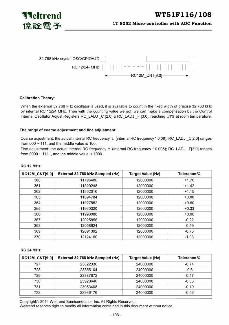
WT51F116/108 1T 8052 Micro-controller with ADC Function
Copyright 2014 Weltrend Semiconductor, Inc. All Rights Reserved. Weltrend reserves right to modify all information contained in this document without notice.
- 106 -
RC12M_CNT[9:0]
32.768 kHz crystal OSC/GPIOA4D
RC 12/24- MHz ................
Calibration Theory:
When the external 32.768 kHz oscillator is used, it is available to count in the fixed width of precise 32.768 kHz by internal RC 12/24 MHz. Then with the counting value we got, we can make a compensation by the Control Internal Oscillator Adjust Registers RC_LADJ _C [2:0] & RC_LADJ _F [3:0], reaching ±1% at room temperature.
The range of coarse adjustment and fine adjustment:
Coarse adjustment: the actual internal RC frequency ± (internal RC frequency * 0.08); RC_LADJ _C[2:0] ranges from 000 ~ 111, and the middle value is 100. Fine adjustment: the actual internal RC frequency ± (internal RC frequency * 0.005); RC_LADJ _F[3:0] ranges from 0000 ~ 1111, and the middle value is 1000.
RC 12 MHz
RC12M_CNT[9:0] External 32.768 kHz Sampled (Hz) Target Value (Hz) Tolerance % 360 11796480 12000000 +1.70 361 11829248 12000000 +1.42 362 11862016 12000000 +1.15 363 11894784 12000000 +0.88 364 11927552 12000000 +0.60 365 11960320 12000000 +0.33 366 11993088 12000000 +0.06 367 12025856 12000000 -0.22 368 12058624 12000000 -0.49 369 12091392 12000000 -0.76 370 12124160 12000000 -1.03
RC 24 MHz
RC12M_CNT[9:0] External 32.768 kHz Sampled (Hz) Target Value (Hz) Tolerance % 727 23822336 24000000 -0.74 728 23855104 24000000 -0.6 729 23887872 24000000 -0.47 730 23920640 24000000 -0.33 731 23953408 24000000 -0.19 732 23986176 24000000 -0.06
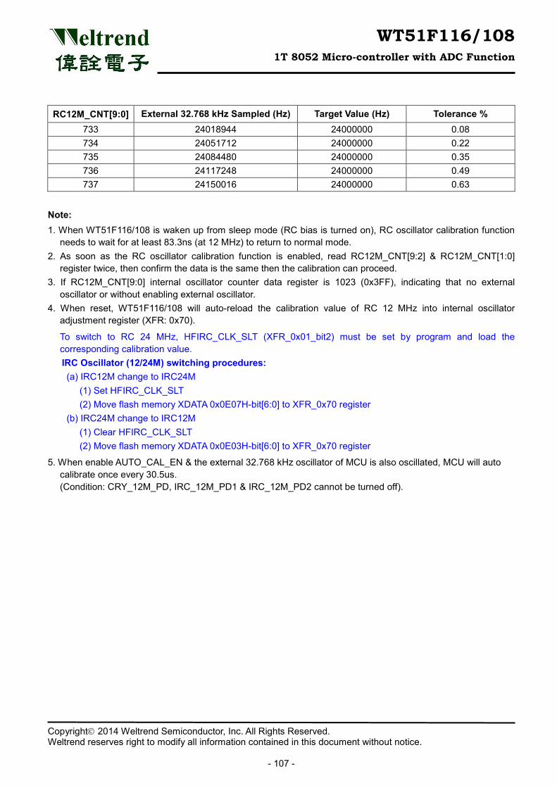
WT51F116/108 1T 8052 Micro-controller with ADC Function
Copyright 2014 Weltrend Semiconductor, Inc. All Rights Reserved. Weltrend reserves right to modify all information contained in this document without notice.
- 107 -
RC12M_CNT[9:0] External 32.768 kHz Sampled (Hz) Target Value (Hz) Tolerance % 733 24018944 24000000 0.08 734 24051712 24000000 0.22 735 24084480 24000000 0.35 736 24117248 24000000 0.49 737 24150016 24000000 0.63
Note: 1. When WT51F116/108 is waken up from sleep mode (RC bias is turned on), RC oscillator calibration function
needs to wait for at least 83.3ns (at 12 MHz) to return to normal mode. 2. As soon as the RC oscillator calibration function is enabled, read RC12M_CNT[9:2] & RC12M_CNT[1:0]
register twice, then confirm the data is the same then the calibration can proceed. 3. If RC12M_CNT[9:0] internal oscillator counter data register is 1023 (0x3FF), indicating that no external
oscillator or without enabling external oscillator. 4. When reset, WT51F116/108 will auto-reload the calibration value of RC 12 MHz into internal oscillator
adjustment register (XFR: 0x70).
To switch to RC 24 MHz, HFIRC_CLK_SLT (XFR_0x01_bit2) must be set by program and load the corresponding calibration value. IRC Oscillator (12/24M) switching procedures: (a) IRC12M change to IRC24M
(1) Set HFIRC_CLK_SLT (2) Move flash memory XDATA 0x0E07H-bit[6:0] to XFR_0x70 register
(b) IRC24M change to IRC12M (1) Clear HFIRC_CLK_SLT (2) Move flash memory XDATA 0x0E03H-bit[6:0] to XFR_0x70 register
5. When enable AUTO_CAL_EN & the external 32.768 kHz oscillator of MCU is also oscillated, MCU will auto calibrate once every 30.5us. (Condition: CRY_12M_PD, IRC_12M_PD1 & IRC_12M_PD2 cannot be turned off).
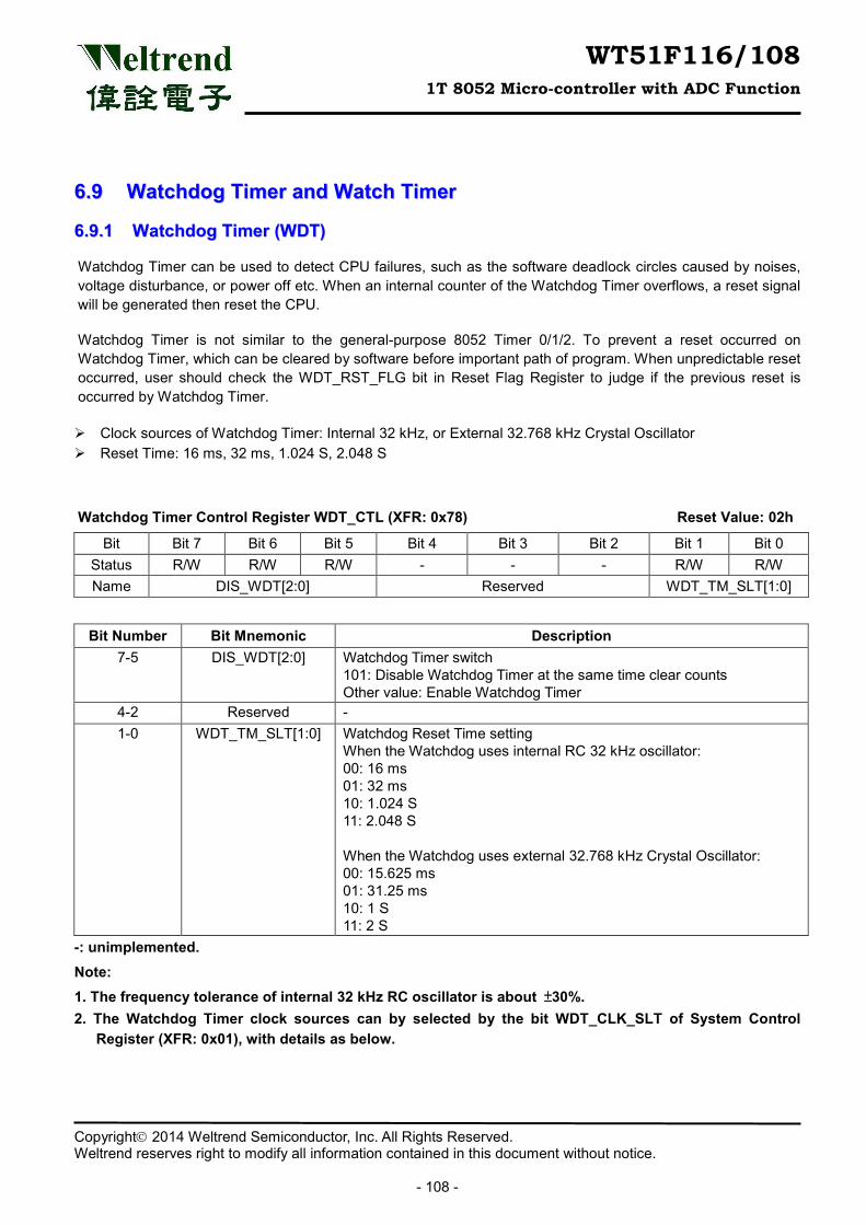
WT51F116/108 1T 8052 Micro-controller with ADC Function
Copyright 2014 Weltrend Semiconductor, Inc. All Rights Reserved. Weltrend reserves right to modify all information contained in this document without notice.
- 108 -
66..99 WWaattcchhddoogg TTiimmeerr aanndd WWaattcchh TTiimmeerr
66..99..11 WWaattcchhddoogg TTiimmeerr ((WWDDTT))
Watchdog Timer can be used to detect CPU failures, such as the software deadlock circles caused by noises, voltage disturbance, or power off etc. When an internal counter of the Watchdog Timer overflows, a reset signal will be generated then reset the CPU. Watchdog Timer is not similar to the general-purpose 8052 Timer 0/1/2. To prevent a reset occurred on Watchdog Timer, which can be cleared by software before important path of program. When unpredictable reset occurred, user should check the WDT_RST_FLG bit in Reset Flag Register to judge if the previous reset is occurred by Watchdog Timer. Clock sources of Watchdog Timer: Internal 32 kHz, or External 32.768 kHz Crystal Oscillator Reset Time: 16 ms, 32 ms, 1.024 S, 2.048 S
Watchdog Timer Control Register WDT_CTL (XFR: 0x78) Reset Value: 02h
Bit Bit 7 Bit 6 Bit 5 Bit 4 Bit 3 Bit 2 Bit 1 Bit 0 Status R/W R/W R/W - - - R/W R/W Name DIS_WDT[2:0] Reserved WDT_TM_SLT[1:0]
Bit Number Bit Mnemonic Description 7-5 DIS_WDT[2:0] Watchdog Timer switch
101: Disable Watchdog Timer at the same time clear counts Other value: Enable Watchdog Timer
4-2 Reserved - 1-0 WDT_TM_SLT[1:0] Watchdog Reset Time setting
When the Watchdog uses internal RC 32 kHz oscillator: 00: 16 ms 01: 32 ms 10: 1.024 S 11: 2.048 S When the Watchdog uses external 32.768 kHz Crystal Oscillator: 00: 15.625 ms 01: 31.25 ms 10: 1 S 11: 2 S
-: unimplemented. Note: 1. The frequency tolerance of internal 32 kHz RC oscillator is about ±30%. 2. The Watchdog Timer clock sources can by selected by the bit WDT_CLK_SLT of System Control
Register (XFR: 0x01), with details as below.
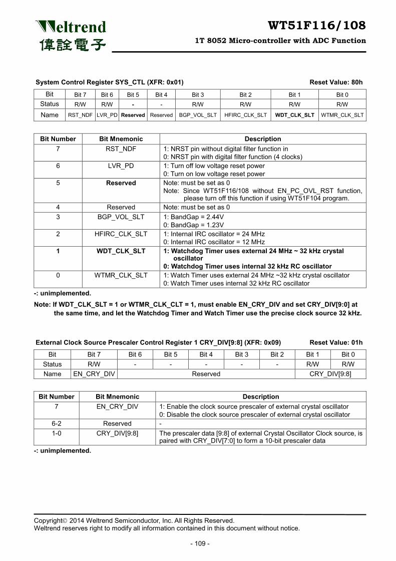
WT51F116/108 1T 8052 Micro-controller with ADC Function
Copyright 2014 Weltrend Semiconductor, Inc. All Rights Reserved. Weltrend reserves right to modify all information contained in this document without notice.
- 109 -
System Control Register SYS_CTL (XFR: 0x01) Reset Value: 80h
Bit Bit 7 Bit 6 Bit 5 Bit 4 Bit 3 Bit 2 Bit 1 Bit 0 Status R/W R/W - - R/W R/W R/W R/W
Name RST_NDF LVR_PD Reserved Reserved BGP_VOL_SLT HFIRC_CLK_SLT WDT_CLK_SLT WTMR_CLK_SLT
Bit Number Bit Mnemonic Description 7 RST_NDF 1: NRST pin without digital filter function in
0: NRST pin with digital filter function (4 clocks) 6 LVR_PD 1: Turn off low voltage reset power
0: Turn on low voltage reset power 5 Reserved Note: must be set as 0
Note: Since WT51F116/108 without EN_PC_OVL_RST function, please turn off this function if using WT51F104 program.
4 Reserved Note: must be set as 0 3 BGP_VOL_SLT 1: BandGap = 2.44V
0: BandGap = 1.23V 2 HFIRC_CLK_SLT 1: Internal IRC oscillator = 24 MHz
0: Internal IRC oscillator = 12 MHz 1 WDT_CLK_SLT 1: Watchdog Timer uses external 24 MHz ~ 32 kHz crystal
oscillator 0: Watchdog Timer uses internal 32 kHz RC oscillator
0 WTMR_CLK_SLT 1: Watch Timer uses external 24 MHz ~32 kHz crystal oscillator 0: Watch Timer uses internal 32 kHz RC oscillator
-: unimplemented. Note: If WDT_CLK_SLT = 1 or WTMR_CLK_CLT = 1, must enable EN_CRY_DIV and set CRY_DIV[9:0] at
the same time, and let the Watchdog Timer and Watch Timer use the precise clock source 32 kHz.
External Clock Source Prescaler Control Register 1 CRY_DIV[9:8] (XFR: 0x09) Reset Value: 01h
Bit Bit 7 Bit 6 Bit 5 Bit 4 Bit 3 Bit 2 Bit 1 Bit 0 Status R/W - - - - - R/W R/W Name EN_CRY_DIV Reserved CRY_DIV[9:8]
Bit Number Bit Mnemonic Description 7 EN_CRY_DIV 1: Enable the clock source prescaler of external crystal oscillator
0: Disable the clock source prescaler of external crystal oscillator 6-2 Reserved - 1-0 CRY_DIV[9:8] The prescaler data [9:8] of external Crystal Oscillator Clock source, is
paired with CRY_DIV[7:0] to form a 10-bit prescaler data -: unimplemented.
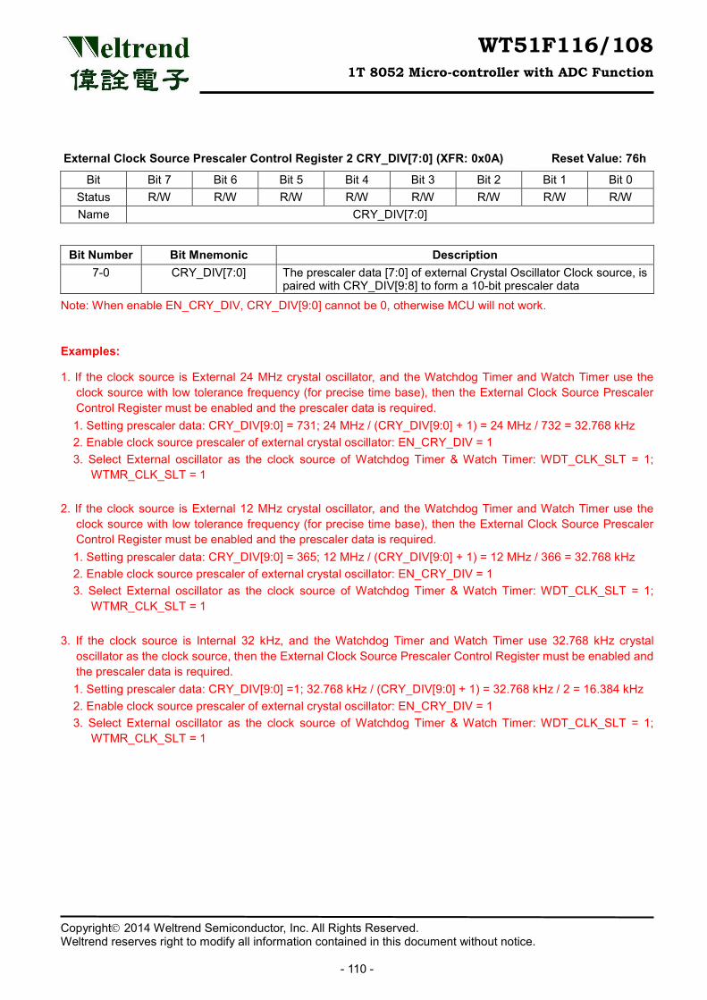
WT51F116/108 1T 8052 Micro-controller with ADC Function
Copyright 2014 Weltrend Semiconductor, Inc. All Rights Reserved. Weltrend reserves right to modify all information contained in this document without notice.
- 110 -
External Clock Source Prescaler Control Register 2 CRY_DIV[7:0] (XFR: 0x0A) Reset Value: 76h
Bit Bit 7 Bit 6 Bit 5 Bit 4 Bit 3 Bit 2 Bit 1 Bit 0 Status R/W R/W R/W R/W R/W R/W R/W R/W Name CRY_DIV[7:0]
Bit Number Bit Mnemonic Description 7-0 CRY_DIV[7:0] The prescaler data [7:0] of external Crystal Oscillator Clock source, is
paired with CRY_DIV[9:8] to form a 10-bit prescaler data Note: When enable EN_CRY_DIV, CRY_DIV[9:0] cannot be 0, otherwise MCU will not work.
Examples:
1. If the clock source is External 24 MHz crystal oscillator, and the Watchdog Timer and Watch Timer use the clock source with low tolerance frequency (for precise time base), then the External Clock Source Prescaler Control Register must be enabled and the prescaler data is required. 1. Setting prescaler data: CRY_DIV[9:0] = 731; 24 MHz / (CRY_DIV[9:0] + 1) = 24 MHz / 732 = 32.768 kHz 2. Enable clock source prescaler of external crystal oscillator: EN_CRY_DIV = 1 3. Select External oscillator as the clock source of Watchdog Timer & Watch Timer: WDT_CLK_SLT = 1;
WTMR_CLK_SLT = 1
2. If the clock source is External 12 MHz crystal oscillator, and the Watchdog Timer and Watch Timer use the clock source with low tolerance frequency (for precise time base), then the External Clock Source Prescaler Control Register must be enabled and the prescaler data is required. 1. Setting prescaler data: CRY_DIV[9:0] = 365; 12 MHz / (CRY_DIV[9:0] + 1) = 12 MHz / 366 = 32.768 kHz 2. Enable clock source prescaler of external crystal oscillator: EN_CRY_DIV = 1 3. Select External oscillator as the clock source of Watchdog Timer & Watch Timer: WDT_CLK_SLT = 1;
WTMR_CLK_SLT = 1 3. If the clock source is Internal 32 kHz, and the Watchdog Timer and Watch Timer use 32.768 kHz crystal
oscillator as the clock source, then the External Clock Source Prescaler Control Register must be enabled and the prescaler data is required. 1. Setting prescaler data: CRY_DIV[9:0] =1; 32.768 kHz / (CRY_DIV[9:0] + 1) = 32.768 kHz / 2 = 16.384 kHz 2. Enable clock source prescaler of external crystal oscillator: EN_CRY_DIV = 1 3. Select External oscillator as the clock source of Watchdog Timer & Watch Timer: WDT_CLK_SLT = 1;
WTMR_CLK_SLT = 1
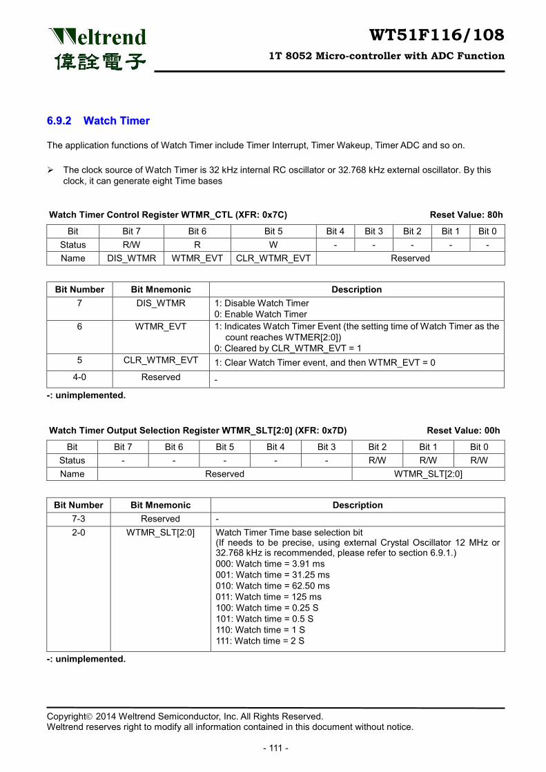
WT51F116/108 1T 8052 Micro-controller with ADC Function
Copyright 2014 Weltrend Semiconductor, Inc. All Rights Reserved. Weltrend reserves right to modify all information contained in this document without notice.
- 111 -
66..99..22 WWaattcchh TTiimmeerr
The application functions of Watch Timer include Timer Interrupt, Timer Wakeup, Timer ADC and so on. The clock source of Watch Timer is 32 kHz internal RC oscillator or 32.768 kHz external oscillator. By this
clock, it can generate eight Time bases Watch Timer Control Register WTMR_CTL (XFR: 0x7C) Reset Value: 80h
Bit Bit 7 Bit 6 Bit 5 Bit 4 Bit 3 Bit 2 Bit 1 Bit 0 Status R/W R W - - - - - Name DIS_WTMR WTMR_EVT CLR_WTMR_EVT Reserved
Bit Number Bit Mnemonic Description 7 DIS_WTMR 1: Disable Watch Timer
0: Enable Watch Timer 6 WTMR_EVT 1: Indicates Watch Timer Event (the setting time of Watch Timer as the
count reaches WTMER[2:0]) 0: Cleared by CLR_WTMR_EVT = 1
5 CLR_WTMR_EVT 1: Clear Watch Timer event, and then WTMR_EVT = 0 4-0 Reserved -
-: unimplemented.
Watch Timer Output Selection Register WTMR_SLT[2:0] (XFR: 0x7D) Reset Value: 00h
Bit Bit 7 Bit 6 Bit 5 Bit 4 Bit 3 Bit 2 Bit 1 Bit 0 Status - - - - - R/W R/W R/W Name Reserved WTMR_SLT[2:0]
Bit Number Bit Mnemonic Description 7-3 Reserved - 2-0 WTMR_SLT[2:0] Watch Timer Time base selection bit
(If needs to be precise, using external Crystal Oscillator 12 MHz or 32.768 kHz is recommended, please refer to section 6.9.1.) 000: Watch time = 3.91 ms 001: Watch time = 31.25 ms 010: Watch time = 62.50 ms 011: Watch time = 125 ms 100: Watch time = 0.25 S 101: Watch time = 0.5 S 110: Watch time = 1 S 111: Watch time = 2 S
-: unimplemented.
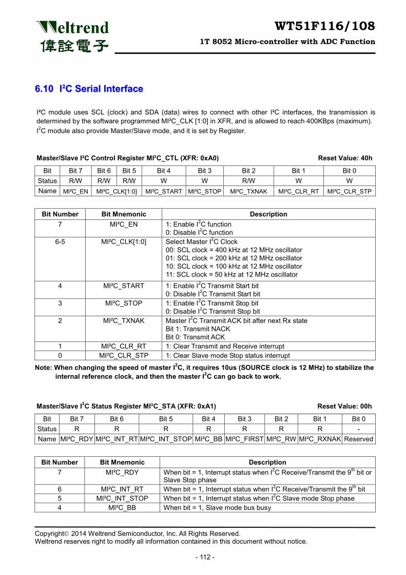
WT51F116/108 1T 8052 Micro-controller with ADC Function
Copyright 2014 Weltrend Semiconductor, Inc. All Rights Reserved. Weltrend reserves right to modify all information contained in this document without notice.
- 112 -
66..1100 II²²CC SSeerriiaall IInntteerrffaaccee
I²C module uses SCL (clock) and SDA (data) wires to connect with other I²C interfaces, the transmission is determined by the software programmed MI²C_CLK [1:0] in XFR, and is allowed to reach 400KBps (maximum). I2C module also provide Master/Slave mode, and it is set by Register.
Master/Slave I²C Control Register MI²C_CTL (XFR: 0xA0) Reset Value: 40h
Bit Bit 7 Bit 6 Bit 5 Bit 4 Bit 3 Bit 2 Bit 1 Bit 0 Status R/W R/W R/W W W R/W W W Name MI²C_EN MI²C_CLK[1:0] MI²C_START MI²C_STOP MI²C_TXNAK MI²C_CLR_RT MI²C_CLR_STP
Bit Number Bit Mnemonic Description 7 MI²C_EN 1: Enable I2C function
0: Disable I2C function 6-5 MI²C_CLK[1:0] Select Master I2C Clock
00: SCL clock = 400 kHz at 12 MHz oscillator 01: SCL clock = 200 kHz at 12 MHz oscillator 10: SCL clock = 100 kHz at 12 MHz oscillator 11: SCL clock = 50 kHz at 12 MHz oscillator
4 MI²C_START 1: Enable I2C Transmit Start bit 0: Disable I2C Transmit Start bit
3 MI²C_STOP 1: Enable I2C Transmit Stop bit 0: Disable I2C Transmit Stop bit
2 MI²C_TXNAK Master I2C Transmit ACK bit after next Rx state Bit 1: Transmit NACK Bit 0: Transmit ACK
1 MI²C_CLR_RT 1: Clear Transmit and Receive interrupt 0 MI²C_CLR_STP 1: Clear Slave mode Stop status interrupt
Note: When changing the speed of master I2C, it requires 10us (SOURCE clock is 12 MHz) to stabilize the internal reference clock, and then the master I2C can go back to work.
Master/Slave I2C Status Register MI²C_STA (XFR: 0xA1) Reset Value: 00h
Bit Bit 7 Bit 6 Bit 5 Bit 4 Bit 3 Bit 2 Bit 1 Bit 0 Status R R R R R R R - Name MI²C_RDY MI²C_INT_RT MI²C_INT_STOP MI²C_BB MI²C_FIRST MI²C_RW MI²C_RXNAK Reserved
Bit Number Bit Mnemonic Description 7 MI²C_RDY When bit = 1, Interrupt status when I2C Receive/Transmit the 9th bit or
Slave Stop phase 6 MI²C_INT_RT When bit = 1, Interrupt status when I2C Receive/Transmit the 9th bit 5 MI²C_INT_STOP When bit = 1, Interrupt status when I2C Slave mode Stop phase 4 MI²C_BB When bit = 1, Slave mode bus busy
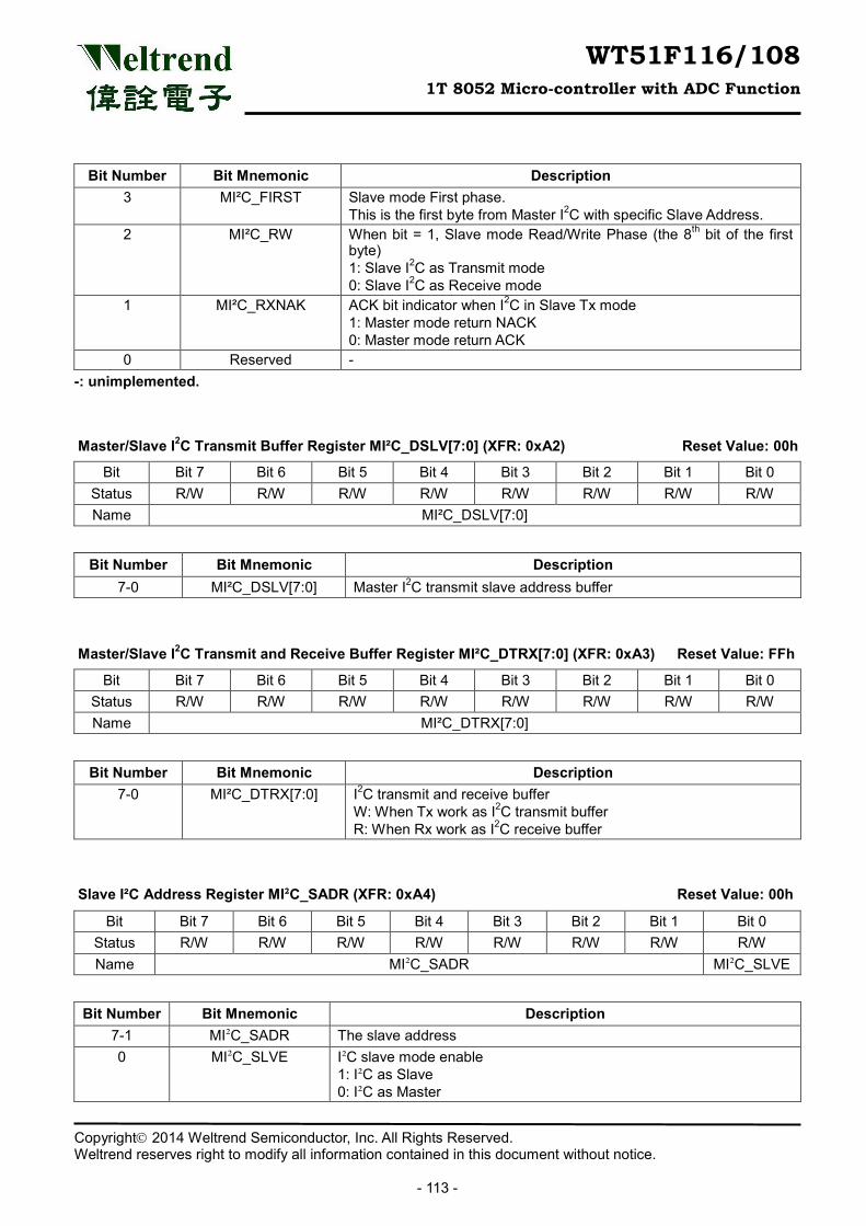
WT51F116/108 1T 8052 Micro-controller with ADC Function
Copyright 2014 Weltrend Semiconductor, Inc. All Rights Reserved. Weltrend reserves right to modify all information contained in this document without notice.
- 113 -
Bit Number Bit Mnemonic Description 3 MI²C_FIRST Slave mode First phase.
This is the first byte from Master I2C with specific Slave Address. 2 MI²C_RW When bit = 1, Slave mode Read/Write Phase (the 8th bit of the first
byte) 1: Slave I2C as Transmit mode 0: Slave I2C as Receive mode
1 MI²C_RXNAK ACK bit indicator when I2C in Slave Tx mode 1: Master mode return NACK 0: Master mode return ACK
0 Reserved - -: unimplemented.
Master/Slave I2C Transmit Buffer Register MI²C_DSLV[7:0] (XFR: 0xA2) Reset Value: 00h
Bit Bit 7 Bit 6 Bit 5 Bit 4 Bit 3 Bit 2 Bit 1 Bit 0 Status R/W R/W R/W R/W R/W R/W R/W R/W Name MI²C_DSLV[7:0]
Bit Number Bit Mnemonic Description 7-0 MI²C_DSLV[7:0] Master I2C transmit slave address buffer
Master/Slave I2C Transmit and Receive Buffer Register MI²C_DTRX[7:0] (XFR: 0xA3) Reset Value: FFh
Bit Bit 7 Bit 6 Bit 5 Bit 4 Bit 3 Bit 2 Bit 1 Bit 0 Status R/W R/W R/W R/W R/W R/W R/W R/W Name MI²C_DTRX[7:0]
Bit Number Bit Mnemonic Description 7-0 MI²C_DTRX[7:0] I2C transmit and receive buffer
W: When Tx work as I2C transmit buffer R: When Rx work as I2C receive buffer
Slave I²C Address Register MI²C_SADR (XFR: 0xA4) Reset Value: 00h
Bit Bit 7 Bit 6 Bit 5 Bit 4 Bit 3 Bit 2 Bit 1 Bit 0 Status R/W R/W R/W R/W R/W R/W R/W R/W Name MI²C_SADR MI²C_SLVE
Bit Number Bit Mnemonic Description 7-1 MI²C_SADR The slave address 0 MI²C_SLVE I²C slave mode enable
1: I²C as Slave 0: I²C as Master
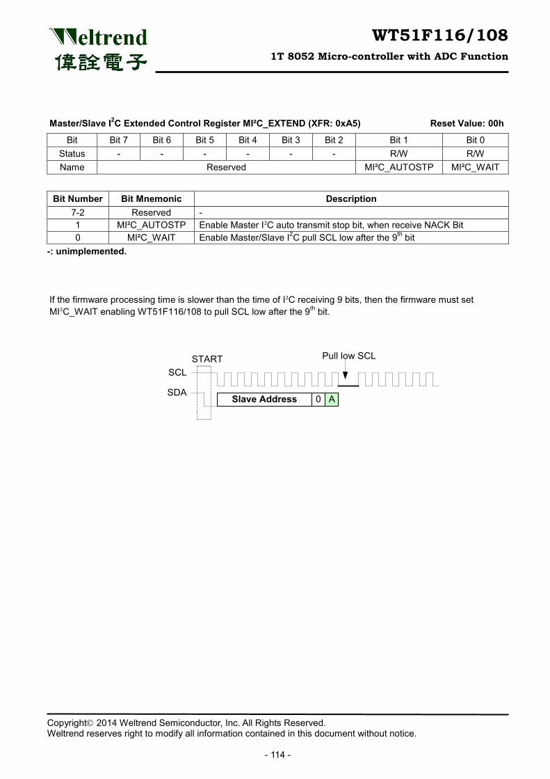
WT51F116/108 1T 8052 Micro-controller with ADC Function
Copyright 2014 Weltrend Semiconductor, Inc. All Rights Reserved. Weltrend reserves right to modify all information contained in this document without notice.
- 114 -
Master/Slave I2C Extended Control Register MI²C_EXTEND (XFR: 0xA5) Reset Value: 00h
Bit Bit 7 Bit 6 Bit 5 Bit 4 Bit 3 Bit 2 Bit 1 Bit 0 Status - - - - - - R/W R/W Name Reserved MI²C_AUTOSTP MI²C_WAIT
Bit Number Bit Mnemonic Description 7-2 Reserved - 1 MI²C_AUTOSTP Enable Master I²C auto transmit stop bit, when receive NACK Bit 0 MI²C_WAIT Enable Master/Slave I2C pull SCL low after the 9th bit
-: unimplemented.
If the firmware processing time is slower than the time of I²C receiving 9 bits, then the firmware must set MI²C_WAIT enabling WT51F116/108 to pull SCL low after the 9th bit.
Slave Address 0 A
Pull low SCL
SCL
SDA
START
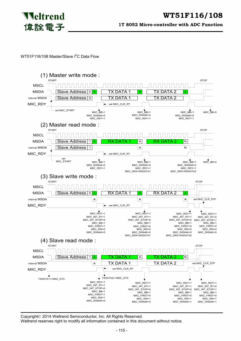
WT51F116/108 1T 8052 Micro-controller with ADC Function
Copyright 2014 Weltrend Semiconductor, Inc. All Rights Reserved. Weltrend reserves right to modify all information contained in this document without notice.
- 115 -
WT51F116/108 Master/Slave I2C Data Flow
(1) Master write mode :
Slave Address A0 TX DATA 1 A TX DATA 2 A
(2) Master read mode :
Slave Address A1 RX DATA 1 A RX DATA 2 N
Slave Address 0 TX DATA 1 TX DATA 2
Slave Address 1
(3) Slave write mode :
Slave Address A0 RX DATA 1 A RX DATA 2 A
(4) Slave read mode :
Slave Address A1 TX DATA 1 A TX DATA 2 N
TX DATA 1 TX DATA 2
START STOP
MSCL
MSDA
MIIC_RDY
internal MSDA
set MIIC_START
set MIIC_CLR_RT
MSCL
MSDA
MIIC_RDY
internal MSDA
MSCL
MSDA
MIIC_RDY
internal MSDA
MSCL
MSDA
MIIC_RDY
internal MSDA
set MIIC_START
START STOP
MIIC_BB=1MIIC_RXNAK=0
MIIC_RDY=1
MIIC_BB=0MIIC_BB=1MIIC_RXNAK=0
MIIC_RDY=1
MIIC_BB=1MIIC_RXNAK=0
MIIC_RDY=1
A N
MIIC_BB=1MIIC_RXNAK=0
MIIC_RDY=1
MIIC_BB=0MIIC_BB=1MIIC_RXNAK=0
MIIC_RDY=1
MIIC_BB=1MIIC_RXNAK=0
MIIC_RDY=1
START STOP
set MIIC_CLR_RT
A A A
MIIC_BB=1
MIIC_RXNAK=0
MIIC_RDY=1
MIIC_RW=0MIIC_FIRST=1
MIIC_BB=1
MIIC_RXNAK=0MIIC_RW=0
MIIC_FIRST=0MIIC_BB=1
MIIC_RXNAK=0MIIC_RW=0
MIIC_FIRST=0MIIC_BB=1
MIIC_RXNAK=0MIIC_RW=0
MIIC_FIRST=0
START STOP
A
set MIIC_CLR_RT
MIIC_BB=1
MIIC_RXNAK=0
MIIC_RDY=1
MIIC_RW=1MIIC_FIRST=1
MIIC_BB=1
MIIC_RXNAK=0
MIIC_RDY=1
MIIC_RW=1MIIC_FIRST=0
MIIC_BB=1
MIIC_RXNAK=1
MIIC_RDY=1
MIIC_RW=1MIIC_FIRST=0
MIIC_DRX=RXDATA1 MIIC_DRX=RXDATA2
set MIIC_CLR_RT
MIIC_DRX=RXDATA1 MIIC_DRX=RXDATA2
set MIIC_CLR_STP
TXDATA1=>MIIC_DTX
MIIC_BB=1
MIIC_RXNAK=1
MIIC_RDY=1
MIIC_RW=1MIIC_FIRST=0
MIIC_INT_STOP=0MIIC_INT_RT=1
MIIC_RDY=1
MIIC_INT_STOP=0MIIC_INT_RT=1
MIIC_RDY=1
MIIC_INT_STOP=0MIIC_INT_RT=1
MIIC_RDY=1MIIC_INT_RT=0
MIIC_INT_STOP=1
MIIC_INT_STOP=0MIIC_INT_RT=1
MIIC_INT_STOP=0MIIC_INT_RT=1
MIIC_INT_STOP=0MIIC_INT_RT=1
MIIC_INT_STOP=1MIIC_INT_RT=0
set MIIC_CLR_STP
TXDATA2=>MIIC_DTX
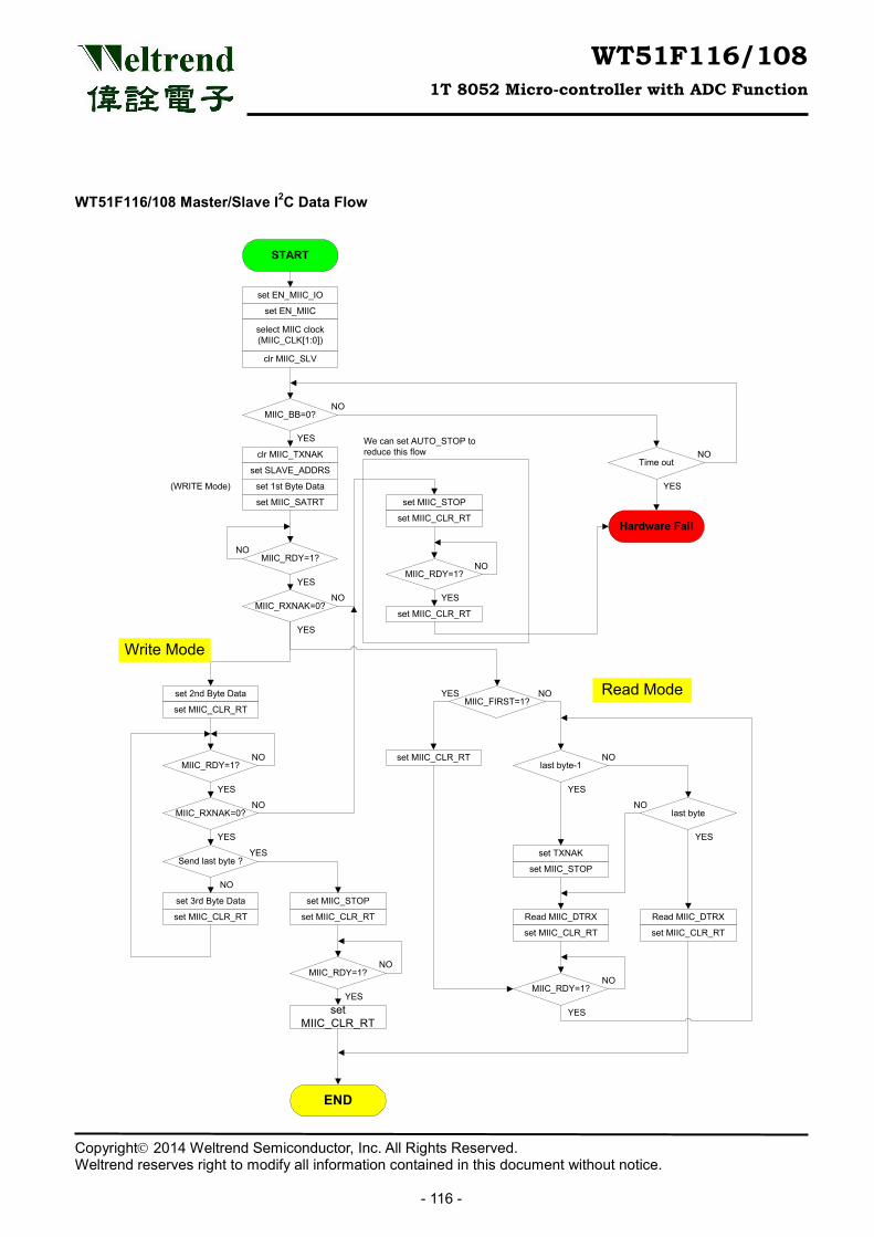
WT51F116/108 1T 8052 Micro-controller with ADC Function
Copyright 2014 Weltrend Semiconductor, Inc. All Rights Reserved. Weltrend reserves right to modify all information contained in this document without notice.
- 116 -
WT51F116/108 Master/Slave I2C Data Flow
set EN_MIIC_IO
set EN_MIIC
select MIIC clock(MIIC_CLK[1:0])
clr MIIC_SLV
MIIC_BB=0?
Time out
Hardware Fail
START
clr MIIC_TXNAK
set SLAVE_ADDRS
set 1st Byte Data
set MIIC_SATRT
(WRITE Mode)
MIIC_RDY=1?
MIIC_RXNAK=0?
set MIIC_STOP
set MIIC_CLR_RT
MIIC_RDY=1?
We can set AUTO_STOP to reduce this flow
set 2nd Byte Data
set MIIC_CLR_RT
MIIC_RDY=1?
MIIC_RXNAK=0?
Send last byte ?
set 3rd Byte Data
set MIIC_CLR_RT
set MIIC_CLR_RT
set MIIC_CLR_RT
MIIC_RDY=1?
set MIIC_CLR_RT
set MIIC_STOP
END
MIIC_FIRST=1?
set MIIC_CLR_RT
Read MIIC_DTRX
set MIIC_CLR_RT
last byte-1
last byte
set MIIC_STOP
set TXNAK
Read MIIC_DTRX
set MIIC_CLR_RT
MIIC_RDY=1?
YES
NO
NO
NO
NO
YES
YES
YES
YES
YES
NO
NO
NO
YES
YES
NO
YES
YES NO
YES
NO
NO
NO
YES
YES
NO
Write Mode
Read Mode
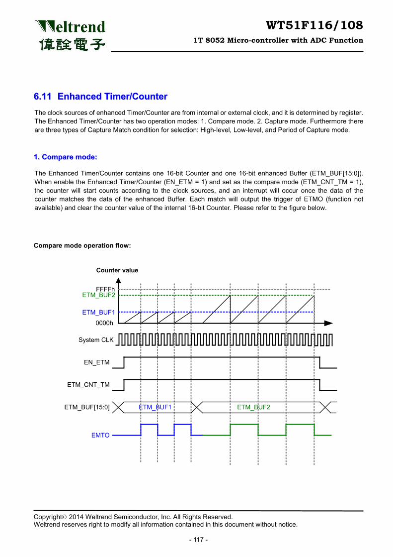
WT51F116/108 1T 8052 Micro-controller with ADC Function
Copyright 2014 Weltrend Semiconductor, Inc. All Rights Reserved. Weltrend reserves right to modify all information contained in this document without notice.
- 117 -
66..1111 EEnnhhaanncceedd TTiimmeerr//CCoouunntteerr The clock sources of enhanced Timer/Counter are from internal or external clock, and it is determined by register. The Enhanced Timer/Counter has two operation modes: 1. Compare mode. 2. Capture mode. Furthermore there are three types of Capture Match condition for selection: High-level, Low-level, and Period of Capture mode.
11.. CCoommppaarree mmooddee::
The Enhanced Timer/Counter contains one 16-bit Counter and one 16-bit enhanced Buffer (ETM_BUF[15:0]). When enable the Enhanced Timer/Counter (EN_ETM = 1) and set as the compare mode (ETM_CNT_TM = 1), the counter will start counts according to the clock sources, and an interrupt will occur once the data of the counter matches the data of the enhanced Buffer. Each match will output the trigger of ETMO (function not available) and clear the counter value of the internal 16-bit Counter. Please refer to the figure below.
Compare mode operation flow:
FFFFh
0000h
Counter value
System CLK
ETM_BUF1
ETM_BUF2
EN_ETM
ETM_CNT_TM
ETM_BUF1 ETM_BUF2ETM_BUF[15:0]
EMTO
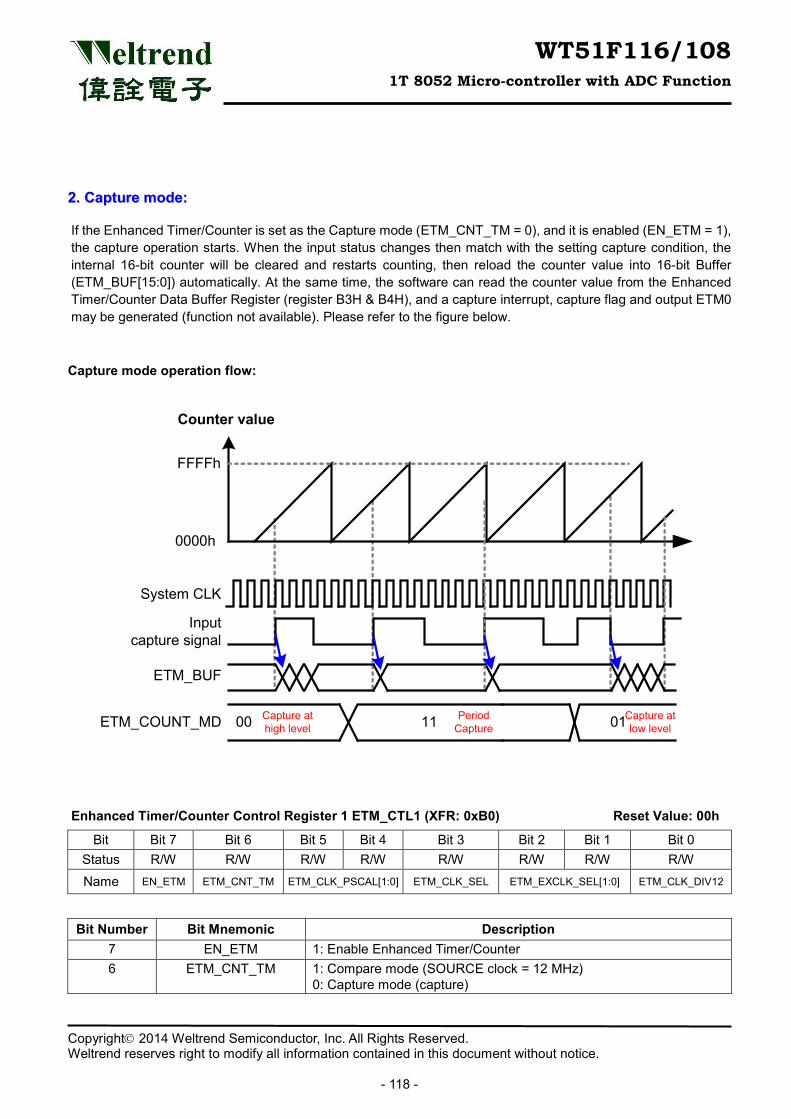
WT51F116/108 1T 8052 Micro-controller with ADC Function
Copyright 2014 Weltrend Semiconductor, Inc. All Rights Reserved. Weltrend reserves right to modify all information contained in this document without notice.
- 118 -
22.. CCaappttuurree mmooddee::
If the Enhanced Timer/Counter is set as the Capture mode (ETM_CNT_TM = 0), and it is enabled (EN_ETM = 1), the capture operation starts. When the input status changes then match with the setting capture condition, the internal 16-bit counter will be cleared and restarts counting, then reload the counter value into 16-bit Buffer (ETM_BUF[15:0]) automatically. At the same time, the software can read the counter value from the Enhanced Timer/Counter Data Buffer Register (register B3H & B4H), and a capture interrupt, capture flag and output ETM0 may be generated (function not available). Please refer to the figure below.
Capture mode operation flow:
FFFFh
0000h
Counter value
Input capture signal
ETM_BUF
System CLK
00 11 01ETM_COUNT_MD Capture at high level
Period Capture
Capture at low level
Enhanced Timer/Counter Control Register 1 ETM_CTL1 (XFR: 0xB0) Reset Value: 00h
Bit Bit 7 Bit 6 Bit 5 Bit 4 Bit 3 Bit 2 Bit 1 Bit 0 Status R/W R/W R/W R/W R/W R/W R/W R/W Name EN_ETM ETM_CNT_TM ETM_CLK_PSCAL[1:0] ETM_CLK_SEL ETM_EXCLK_SEL[1:0] ETM_CLK_DIV12
Bit Number Bit Mnemonic Description 7 EN_ETM 1: Enable Enhanced Timer/Counter 6 ETM_CNT_TM 1: Compare mode (SOURCE clock = 12 MHz)
0: Capture mode (capture)
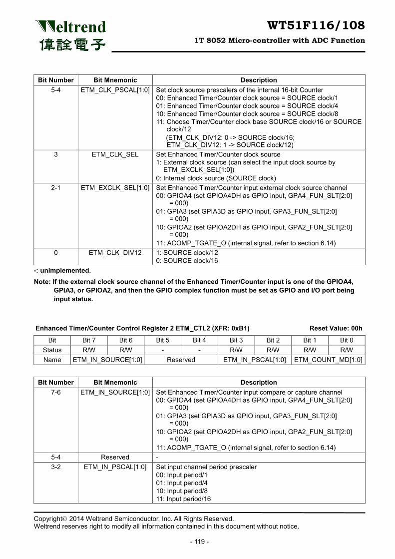
WT51F116/108 1T 8052 Micro-controller with ADC Function
Copyright 2014 Weltrend Semiconductor, Inc. All Rights Reserved. Weltrend reserves right to modify all information contained in this document without notice.
- 119 -
Bit Number Bit Mnemonic Description 5-4 ETM_CLK_PSCAL[1:0] Set clock source prescalers of the internal 16-bit Counter
00: Enhanced Timer/Counter clock source = SOURCE clock/1 01: Enhanced Timer/Counter clock source = SOURCE clock/4 10: Enhanced Timer/Counter clock source = SOURCE clock/8 11: Choose Timer/Counter clock base SOURCE clock/16 or SOURCE
clock/12 (ETM_CLK_DIV12: 0 -> SOURCE clock/16; ETM_CLK_DIV12: 1 -> SOURCE clock/12)
3 ETM_CLK_SEL Set Enhanced Timer/Counter clock source 1: External clock source (can select the input clock source by
ETM_EXCLK_SEL[1:0]) 0: Internal clock source (SOURCE clock)
2-1 ETM_EXCLK_SEL[1:0] Set Enhanced Timer/Counter input external clock source channel 00: GPIOA4 (set GPIOA4DH as GPIO input, GPA4_FUN_SLT[2:0]
= 000) 01: GPIA3 (set GPIA3D as GPIO input, GPA3_FUN_SLT[2:0]
= 000) 10: GPIOA2 (set GPIOA2DH as GPIO input, GPA2_FUN_SLT[2:0]
= 000) 11: ACOMP_TGATE_O (internal signal, refer to section 6.14)
0 ETM_CLK_DIV12 1: SOURCE clock/12 0: SOURCE clock/16
-: unimplemented. Note: If the external clock source channel of the Enhanced Timer/Counter input is one of the GPIOA4,
GPIA3, or GPIOA2, and then the GPIO complex function must be set as GPIO and I/O port being input status.
Enhanced Timer/Counter Control Register 2 ETM_CTL2 (XFR: 0xB1) Reset Value: 00h
Bit Bit 7 Bit 6 Bit 5 Bit 4 Bit 3 Bit 2 Bit 1 Bit 0 Status R/W R/W - - R/W R/W R/W R/W Name ETM_IN_SOURCE[1:0] Reserved ETM_IN_PSCAL[1:0] ETM_COUNT_MD[1:0]
Bit Number Bit Mnemonic Description 7-6 ETM_IN_SOURCE[1:0] Set Enhanced Timer/Counter input compare or capture channel
00: GPIOA4 (set GPIOA4DH as GPIO input, GPA4_FUN_SLT[2:0] = 000)
01: GPIA3 (set GPIA3D as GPIO input, GPA3_FUN_SLT[2:0] = 000)
10: GPIOA2 (set GPIOA2DH as GPIO input, GPA2_FUN_SLT[2:0] = 000)
11: ACOMP_TGATE_O (internal signal, refer to section 6.14) 5-4 Reserved - 3-2 ETM_IN_PSCAL[1:0] Set input channel period prescaler
00: Input period/1 01: Input period/4 10: Input period/8 11: Input period/16
WT51F116/108 1T 8052 Micro-controller with ADC Function
Copyright 2014 Weltrend Semiconductor, Inc. All Rights Reserved. Weltrend reserves right to modify all information contained in this document without notice.
- 120 -
Bit Number Bit Mnemonic Description 1-0 ETM_COUNT_MD[1:0] Capture counting mode selection
00: Capture the interval of high level 01: Capture the interval of low level 1x: Capture the interval period (based on the setting
ETM_IN_PSCAL[1:0] to capture) -: unimplemented. Note: If the external clock source channel of the Enhanced Timer/Counter input is one of the GPIOA4,
GPIA3, or GPIOA2, and then the GPIO complex function must be set as GPIO and I/O port being input status.
Enhanced Timer/Counter Interrupt Register ETM_INT (XFR: 0xB2) Reset Value: 00h
Bit Bit 7 Bit 6 Bit 5 Bit 4 Bit 3 Bit 2 Bit 1 Bit 0 Status R/W R/W R/W R/W R R R - Name EN_CAPINT EN_OVRINT EN_CMPINT CLR_FLAG CAPF OVRF CPMF Reserved
Bit Number Bit Mnemonic Description 7 EN_CAPINT 1: Enable input capture interrupt
0: Disable input capture interrupt 6 EN_OVRINT 1: Enable overflow interrupt
0: Disable overflow interrupt 5 EN_CMPINT 1: Enable Compare Match Interrupt
0: Disable Compare Match Interrupt 4 CLR_FLAG 1: Clear all Enhanced Timer/Counter flags 3 CAPF Input capture flag 2 OVRF Overflow flag
When an overflow occurred in internal 16-bit counter, OVRF = 1 1 CPMF Compare match flag
When internal 16-bit counter has the same value as ETM_BUF, CPMF = 1
0 Reserved - -: unimplemented.
Enhanced Timer/Counter Data Buffer Low Bytes Register ETM_BUF[7:0] (XFR: 0xB3) Reset Value: 00h
Bit Bit 7 Bit 6 Bit 5 Bit 4 Bit 3 Bit 2 Bit 1 Bit 0 Status R/W R/W R/W R/W R/W R/W R/W R/W Name ETM_BUF[7:0]
Bit Number Bit Mnemonic Description 7-0 ETM_BUF[7:0] Paired with ETM_BUF[15:8] to form a 16-bit counter value
Read: In Capture mode, the counter value of the captured input signal Write: In Compare mode, as the compare value to compare with the
internal 16-bit counter
WT51F116/108 1T 8052 Micro-controller with ADC Function
Copyright 2014 Weltrend Semiconductor, Inc. All Rights Reserved. Weltrend reserves right to modify all information contained in this document without notice.
- 121 -
Enhanced Timer/Counter Data Buffer High Bytes Register ETM_BUF[15:8] (XFR: 0xB4) Reset Value: 80h
Bit Bit 7 Bit 6 Bit 5 Bit 4 Bit 3 Bit 2 Bit 1 Bit 0 Status R/W R/W R/W R/W R/W R/W R/W R/W Name ETM_BUF[15:8]
Bit Number Bit Mnemonic Description 7-0 ETM_BUF[15:8] Paired with ETM_BUF[7:0] to from a 16-bit counter value
Read: In Capture mode, the counter value of the captured input signal Write: In Compare mode, as the compare value to compare with the
internal 16-bit counter
Note: In Capture mode, ETM_BUF[15:8] and ETM_BUF[7:0] from a 16-bit counter value, and the counter value should be incremented by one to be the actual counter value in application.
Explanation 1: Due to the internal source goes through the filter, the pulse width of input signal high level and low level must be greater than the width of two SYSTEM Clocks.
Explanation 2: ETM_IN_PSCAL[3:2] = 00: Select Capture Input Source 1 cycle, then the Capture effective Resolution is as below: If Source Clock = 12 MHz, (1/12 MHz)/1 = 83.333 ns; If Source Clock = 24 MHz, (1/24 MHz)/1 = 41.666 ns.
ETM_IN_PSCAL[3:2] = 11: Select Capture Input Source 16 cycles, then the Capture effective Resolution is as below: If Source Clock = 12 MHz, (1/12 MHz)/16 = 5.208 ns; If Source Clock = 24 MHz, (1/24 MHz)/16 = 2.604 ns.
When select Capture 16 cycles allow the enhanced Timer/Counter to get more significant digits, to reduce capture error.
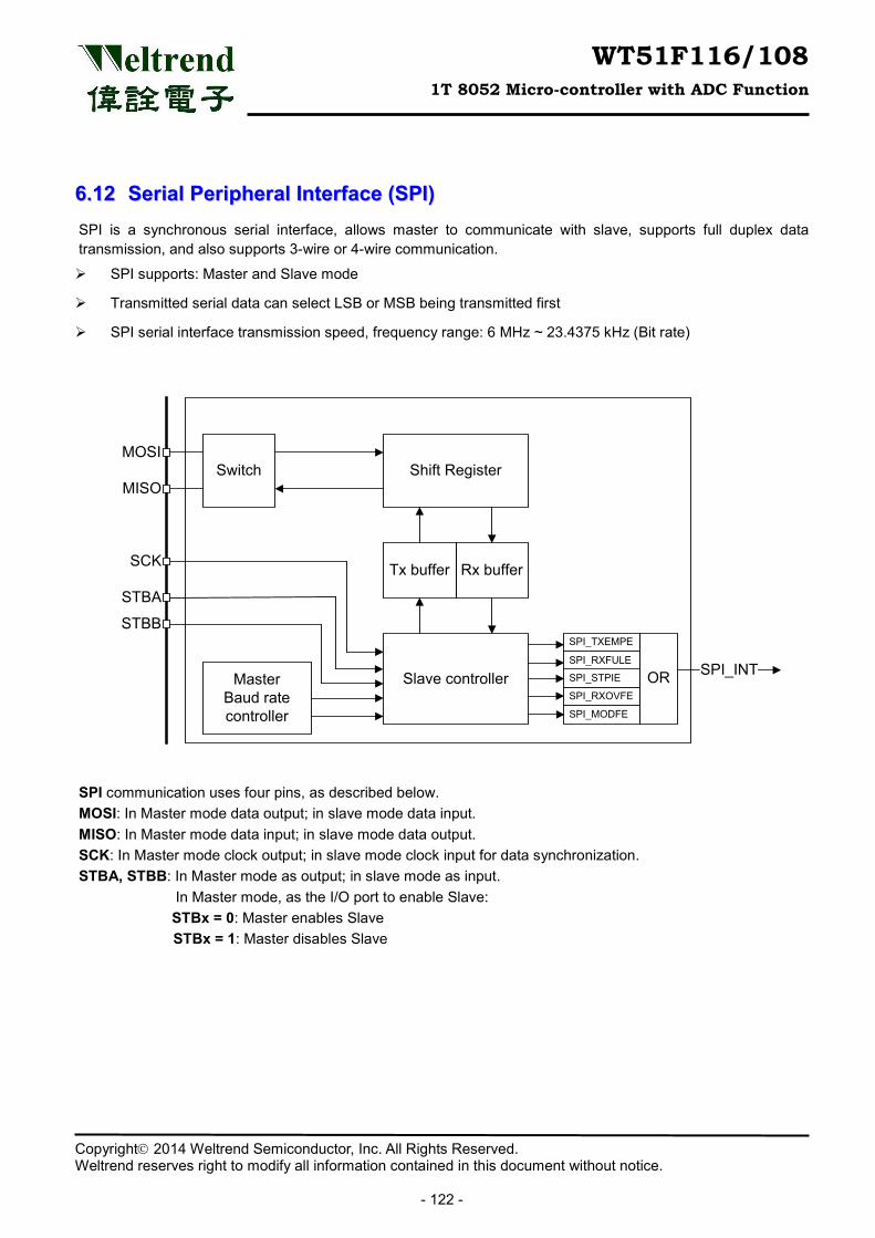
WT51F116/108 1T 8052 Micro-controller with ADC Function
Copyright 2014 Weltrend Semiconductor, Inc. All Rights Reserved. Weltrend reserves right to modify all information contained in this document without notice.
- 122 -
66..1122 SSeerriiaall PPeerriipphheerraall IInntteerrffaaccee ((SSPPII)) SPI is a synchronous serial interface, allows master to communicate with slave, supports full duplex data transmission, and also supports 3-wire or 4-wire communication.
SPI supports: Master and Slave mode
Transmitted serial data can select LSB or MSB being transmitted first
SPI serial interface transmission speed, frequency range: 6 MHz ~ 23.4375 kHz (Bit rate)
Slave controllerMasterBaud rate controller
MOSI
MISOSwitch Shift Register
Rx bufferSCK
STBA
Tx buffer
OR
SPI_TXEMPE
SPI_RXFULESPI_INT
SPI_RXOVFE
SPI_STPIE
SPI_MODFE
STBB
SPI communication uses four pins, as described below. MOSI: In Master mode data output; in slave mode data input. MISO: In Master mode data input; in slave mode data output. SCK: In Master mode clock output; in slave mode clock input for data synchronization. STBA, STBB: In Master mode as output; in slave mode as input. In Master mode, as the I/O port to enable Slave:
STBx = 0: Master enables Slave STBx = 1: Master disables Slave
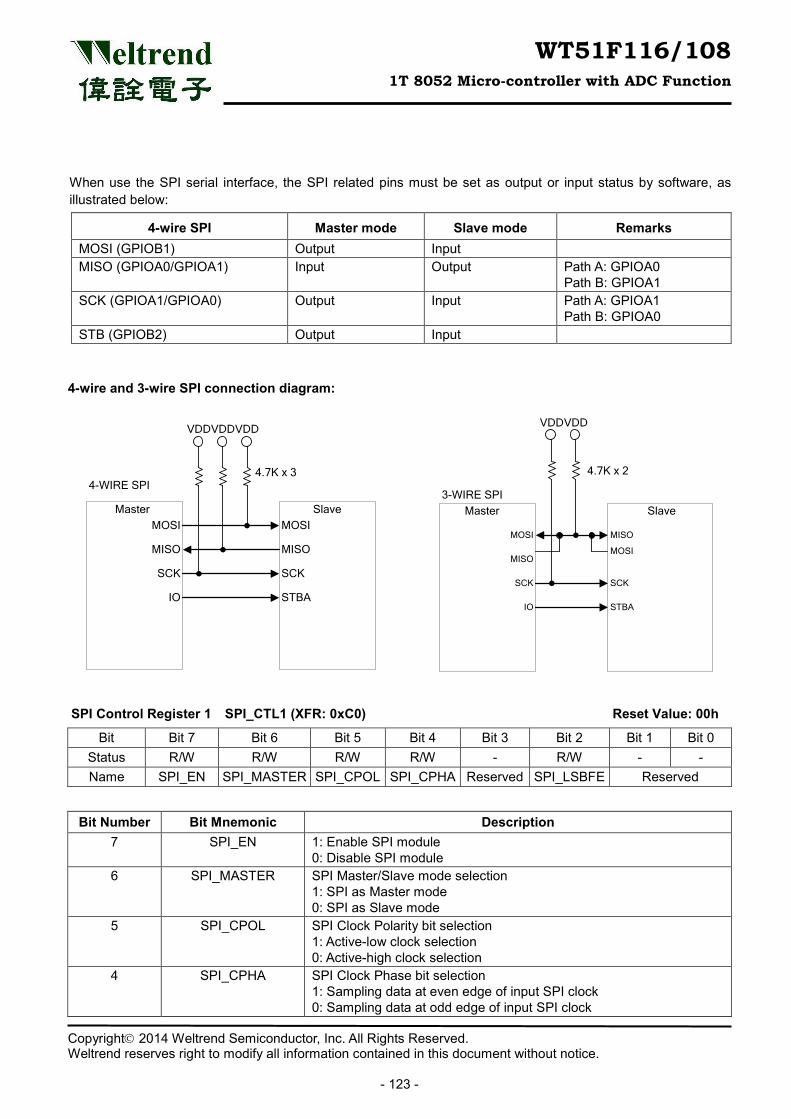
WT51F116/108 1T 8052 Micro-controller with ADC Function
Copyright 2014 Weltrend Semiconductor, Inc. All Rights Reserved. Weltrend reserves right to modify all information contained in this document without notice.
- 123 -
When use the SPI serial interface, the SPI related pins must be set as output or input status by software, as illustrated below:
4-wire SPI Master mode Slave mode Remarks MOSI (GPIOB1) Output Input MISO (GPIOA0/GPIOA1) Input Output Path A: GPIOA0
Path B: GPIOA1 SCK (GPIOA1/GPIOA0) Output Input Path A: GPIOA1
Path B: GPIOA0 STB (GPIOB2) Output Input
4-wire and 3-wire SPI connection diagram:
MOSI
MISO
SCK
IO
Master
MOSI
MISO
SCK
STBA
Slave
MOSI
SCK
IO
Master
MISO
SCK
STBA
Slave
4-WIRE SPI3-WIRE SPI
MISOMOSI
4.7K x 3
VDDVDDVDDVDDVDD
4.7K x 2
SPI Control Register 1 SPI_CTL1 (XFR: 0xC0) Reset Value: 00h
Bit Bit 7 Bit 6 Bit 5 Bit 4 Bit 3 Bit 2 Bit 1 Bit 0 Status R/W R/W R/W R/W - R/W - - Name SPI_EN SPI_MASTER SPI_CPOL SPI_CPHA Reserved SPI_LSBFE Reserved
Bit Number Bit Mnemonic Description 7 SPI_EN 1: Enable SPI module
0: Disable SPI module 6 SPI_MASTER SPI Master/Slave mode selection
1: SPI as Master mode 0: SPI as Slave mode
5 SPI_CPOL SPI Clock Polarity bit selection 1: Active-low clock selection 0: Active-high clock selection
4 SPI_CPHA SPI Clock Phase bit selection 1: Sampling data at even edge of input SPI clock 0: Sampling data at odd edge of input SPI clock
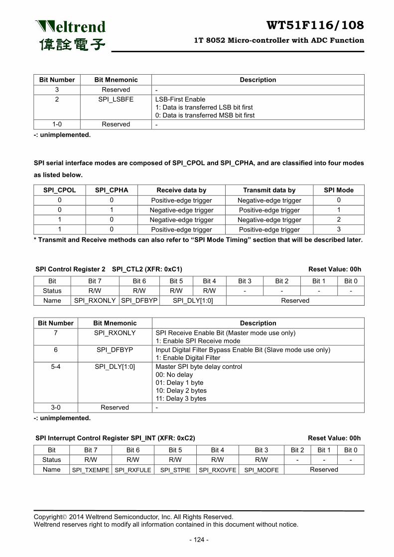
WT51F116/108 1T 8052 Micro-controller with ADC Function
Copyright 2014 Weltrend Semiconductor, Inc. All Rights Reserved. Weltrend reserves right to modify all information contained in this document without notice.
- 124 -
Bit Number Bit Mnemonic Description 3 Reserved - 2 SPI_LSBFE LSB-First Enable
1: Data is transferred LSB bit first 0: Data is transferred MSB bit first
1-0 Reserved - -: unimplemented.
SPI serial interface modes are composed of SPI_CPOL and SPI_CPHA, and are classified into four modes
as listed below.
SPI_CPOL SPI_CPHA Receive data by Transmit data by SPI Mode 0 0 Positive-edge trigger Negative-edge trigger 0 0 1 Negative-edge trigger Positive-edge trigger 1 1 0 Negative-edge trigger Negative-edge trigger 2 1 0 Positive-edge trigger Positive-edge trigger 3
* Transmit and Receive methods can also refer to “SPI Mode Timing” section that will be described later.
SPI Control Register 2 SPI_CTL2 (XFR: 0xC1) Reset Value: 00h
Bit Bit 7 Bit 6 Bit 5 Bit 4 Bit 3 Bit 2 Bit 1 Bit 0 Status R/W R/W R/W R/W - - - - Name SPI_RXONLY SPI_DFBYP SPI_DLY[1:0] Reserved
Bit Number Bit Mnemonic Description 7 SPI_RXONLY SPI Receive Enable Bit (Master mode use only)
1: Enable SPI Receive mode 6 SPI_DFBYP Input Digital Filter Bypass Enable Bit (Slave mode use only)
1: Enable Digital Filter 5-4 SPI_DLY[1:0] Master SPI byte delay control
00: No delay 01: Delay 1 byte 10: Delay 2 bytes 11: Delay 3 bytes
3-0 Reserved - -: unimplemented. SPI Interrupt Control Register SPI_INT (XFR: 0xC2) Reset Value: 00h
Bit Bit 7 Bit 6 Bit 5 Bit 4 Bit 3 Bit 2 Bit 1 Bit 0 Status R/W R/W R/W R/W R/W - - - Name SPI_TXEMPE SPI_RXFULE SPI_STPIE SPI_RXOVFE SPI_MODFE Reserved
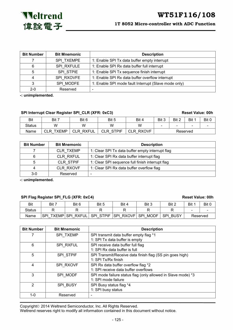
WT51F116/108 1T 8052 Micro-controller with ADC Function
Copyright 2014 Weltrend Semiconductor, Inc. All Rights Reserved. Weltrend reserves right to modify all information contained in this document without notice.
- 125 -
Bit Number Bit Mnemonic Description 7 SPI_TXEMPE 1: Enable SPI Tx data buffer empty interrupt 6 SPI_RXFULE 1: Enable SPI Rx data buffer full interrupt 5 SPI_STPIE 1: Enable SPI Tx sequence finish interrupt 4 SPI_RXOVFE 1: Enable SPI Rx data buffer overflow interrupt 3 SPI_MODFE 1: Enable SPI mode fault Interrupt (Slave mode only)
2-0 Reserved - -: unimplemented.
SPI Interrupt Clear Register SPI_CLR (XFR: 0xC3) Reset Value: 00h
Bit Bit 7 Bit 6 Bit 5 Bit 4 Bit 3 Bit 2 Bit 1 Bit 0 Status W W W W - - - - Name CLR_TXEMP CLR_RXFUL CLR_STPIF CLR_RXOVF Reserved
Bit Number Bit Mnemonic Description 7 CLR_TXEMP 1: Clear SPI Tx data buffer empty interrupt flag 6 CLR_RXFUL 1: Clear SPI Rx data buffer interrupt flag 5 CLR_STPIF 1: Clear SPI sequence full finish interrupt flag 4 CLR_RXOVF 1: Clear SPI Rx data buffer overflow flag
3-0 Reserved - -: unimplemented.
SPI Flag Register SPI_FLG (XFR: 0xC4) Reset Value: 00h
Bit Bit 7 Bit 6 Bit 5 Bit 4 Bit 3 Bit 2 Bit 1 Bit 0 Status R R R R R R - - Name SPI_TXEMP SPI_RXFUL SPI_STPIF SPI_RXOVF SPI_MODF SPI_BUSY Reserved
Bit Number Bit Mnemonic Description 7 SPI_TXEMP SPI transmit data buffer empty flag *1
1: SPI Tx data buffer is empty 6 SPI_RXFUL SPI receive data buffer full flag
1: SPI Rx data buffer is full 5 SPI_STPIF SPI Transmit/Receive data finish flag (SS pin goes high)
1: SPI Tx/Rx finish 4 SPI_RXOVF SPI Rx data buffer overflow flag *2
1: SPI receive data buffer overflows 3 SPI_MODF SPI mode failure status flag (only allowed in Slave mode) *3
1: SPI mode failure 2 SPI_BUSY SPI Busy status flag *4
1: SPI busy status 1-0 Reserved -
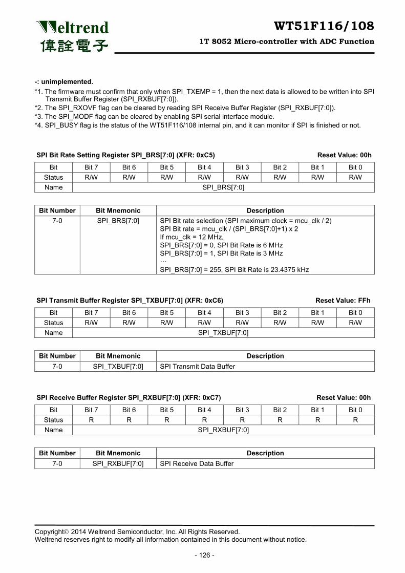
WT51F116/108 1T 8052 Micro-controller with ADC Function
Copyright 2014 Weltrend Semiconductor, Inc. All Rights Reserved. Weltrend reserves right to modify all information contained in this document without notice.
- 126 -
-: unimplemented. *1. The firmware must confirm that only when SPI_TXEMP = 1, then the next data is allowed to be written into SPI
Transmit Buffer Register (SPI_RXBUF[7:0]). *2. The SPI_RXOVF flag can be cleared by reading SPI Receive Buffer Register (SPI_RXBUF[7:0]). *3. The SPI_MODF flag can be cleared by enabling SPI serial interface module. *4. SPI_BUSY flag is the status of the WT51F116/108 internal pin, and it can monitor if SPI is finished or not.
SPI Bit Rate Setting Register SPI_BRS[7:0] (XFR: 0xC5) Reset Value: 00h
Bit Bit 7 Bit 6 Bit 5 Bit 4 Bit 3 Bit 2 Bit 1 Bit 0 Status R/W R/W R/W R/W R/W R/W R/W R/W Name SPI_BRS[7:0]
Bit Number Bit Mnemonic Description 7-0 SPI_BRS[7:0] SPI Bit rate selection (SPI maximum clock = mcu_clk / 2)
SPI Bit rate = mcu_clk / (SPI_BRS[7:0]+1) x 2 If mcu_clk = 12 MHz, SPI_BRS[7:0] = 0, SPI Bit Rate is 6 MHz SPI_BRS[7:0] = 1, SPI Bit Rate is 3 MHz … SPI_BRS[7:0] = 255, SPI Bit Rate is 23.4375 kHz
SPI Transmit Buffer Register SPI_TXBUF[7:0] (XFR: 0xC6) Reset Value: FFh
Bit Bit 7 Bit 6 Bit 5 Bit 4 Bit 3 Bit 2 Bit 1 Bit 0 Status R/W R/W R/W R/W R/W R/W R/W R/W Name SPI_TXBUF[7:0]
Bit Number Bit Mnemonic Description 7-0 SPI_TXBUF[7:0] SPI Transmit Data Buffer
SPI Receive Buffer Register SPI_RXBUF[7:0] (XFR: 0xC7) Reset Value: 00h
Bit Bit 7 Bit 6 Bit 5 Bit 4 Bit 3 Bit 2 Bit 1 Bit 0 Status R R R R R R R R Name SPI_RXBUF[7:0]
Bit Number Bit Mnemonic Description 7-0 SPI_RXBUF[7:0] SPI Receive Data Buffer
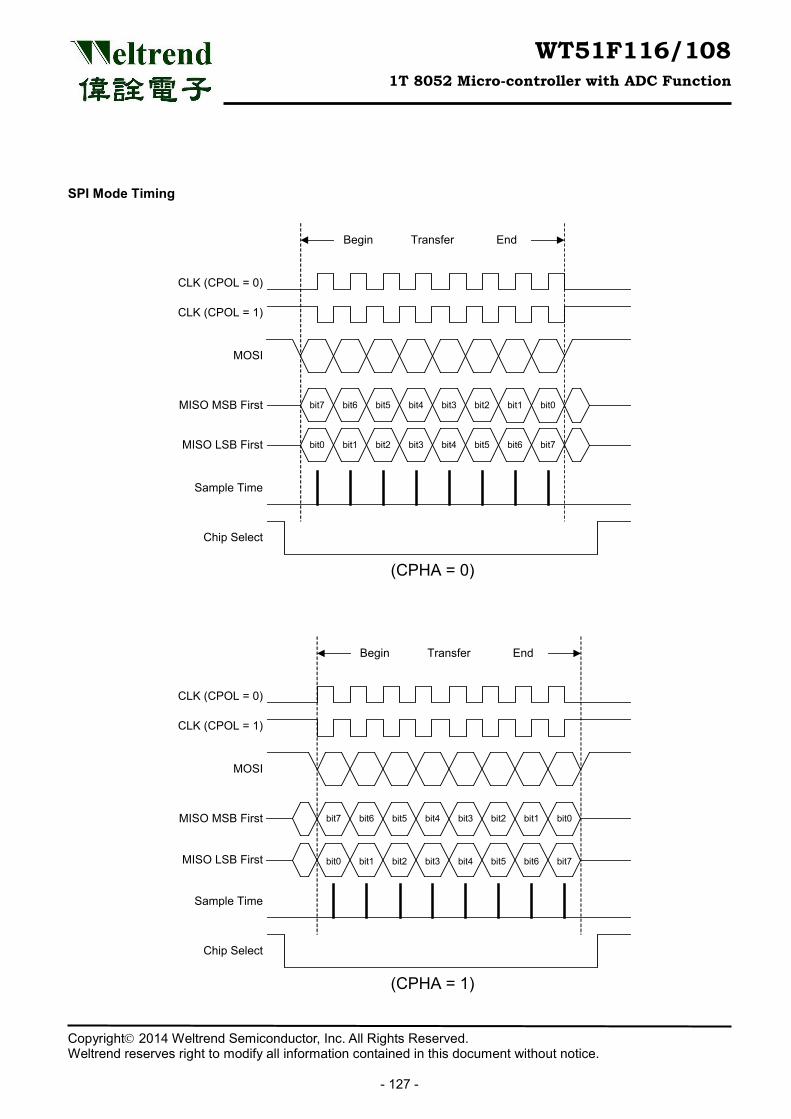
WT51F116/108 1T 8052 Micro-controller with ADC Function
Copyright 2014 Weltrend Semiconductor, Inc. All Rights Reserved. Weltrend reserves right to modify all information contained in this document without notice.
- 127 -
SPI Mode Timing
Begin EndTransfer
CLK (CPOL = 0)
CLK (CPOL = 1)
MOSI
MISO MSB First
Sample Time
Chip Select
(CPHA = 0)
Begin EndTransfer
CLK (CPOL = 0)
CLK (CPOL = 1)
MOSI
MISO MSB First
Sample Time
Chip Select
(CPHA = 1)
bit7 bit6 bit5 bit4 bit3 bit2 bit1 bit0
MISO LSB First bit0 bit1 bit2 bit3 bit4 bit5 bit6 bit7
MISO LSB First bit0 bit1 bit2 bit3 bit4 bit5 bit6 bit7
bit7 bit6 bit5 bit4 bit3 bit2 bit1 bit0
WT51F116/108 1T 8052 Micro-controller with ADC Function
Copyright 2014 Weltrend Semiconductor, Inc. All Rights Reserved. Weltrend reserves right to modify all information contained in this document without notice.
- 128 -
66..1133 AAnnaalloogg//DDiiggiittaall CCoonnvveerrtteerr ((AADDCC)) WT51F116/108 has a built-in 16-channel 10-bit Analog/Digital Converter, and it also provides four conversion modes (Single, Continuous, Voltage Compare, and Timer Auto mode) and four conversion rate (1 MHz, 500 kHz, 125 kHz, and 31.25 kHz) for selection.
The conversion time of A/D Converter is 16us (sampled time 6 us + conversion time 10 us) based on the conversion rate of 1 MHz
Reference Voltage sources VREF have three selections: Power Voltage VDD, Built-in voltage reference VBGAP, and External voltage reference VREF
SSiinnggllee MMooddee::
Turn on the A/D converter power (XFR: 0xD0 ADC_CTL, and ADC_PD = 0), and set the ADC_SINGLE_CVT = 1, then the A/D conversion starts. When ADC_SINGLE_CVT = 0, the conversion is finished. When conversion is completed, the conversion data will be updated and an interrupt will generate (ADFINSH_FLG = 1). If ADC convert finish Interrupt is enabled (EN_ADFINSH_INT = 1), the ADC interrupt will generate.
CCoonnttiinnuuoouuss MMooddee::
If activate continuous convert control bit ADC_CNTNU_CVT = 1, the system will enter the Continuous Conversion Mode.
VVoollttaaggee CCoommppaarree MMooddee::
When turn on the A/D converter power (XFR: 0xD0 ADC_CTL, and ADC Control Register ADC_PD = 0), and activate the Compare function (EN_ADC_CMP = 1), the conversion data of Analog input compare 10-bit setting of XFR: 0xD4 & 0xD5 (ADC_CMP_V). When the corresponding digital value of the voltage analog input is greater than (ADC_BIG = 0) or smaller than (ADC_BIG = 1) the setting value of ADC_CMP_V register, the ADC interrupt will occur. The Voltage Compare function of A/D Converter module worked as a wakeup source. In addition, working together with XFR: 0xD1 ADC_SEL & ADCMP_TM to define ADC turn on time for power-saving purpose.
TTiimmeerr AAuuttoo MMooddee::
When turn on the ADC_AUTO_CVT and work together with the setting of Watch Timer, each Timer event will automatically activate ADC for one-time conversion.
Note: When selecting this mode, the Converting frequency can only select 31.25 kHz (ADC_CLK_SEL[1:0]=11) to get the accurate converting result if the Reference Voltage source is VBGAP.
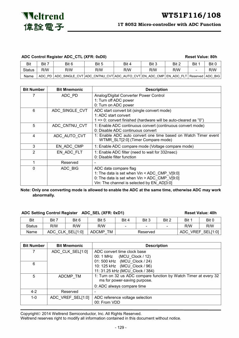
WT51F116/108 1T 8052 Micro-controller with ADC Function
Copyright 2014 Weltrend Semiconductor, Inc. All Rights Reserved. Weltrend reserves right to modify all information contained in this document without notice.
- 129 -
ADC Control Register ADC_CTL (XFR: 0xD0) Reset Value: 80h
Bit Bit 7 Bit 6 Bit 5 Bit 4 Bit 3 Bit 2 Bit 1 Bit 0 Status R/W R/W R/W R/W R/W R/W - R/W Name ADC_PD ADC_SINGLE_CVT ADC_CNTNU_CVT ADC_AUTO_CVT EN_ADC_CMP EN_ADC_FLT Reserved ADC_BIG
Bit Number Bit Mnemonic Description 7 ADC_PD Analog/Digital Converter Power Control
1: Turn off ADC power 0: Turn on ADC power
6 ADC_SINGLE_CVT ADC start convert bit (single convert mode) 1: ADC start convert 1 => 0: convert finished (hardware will be auto-cleared as ”0”)
5 ADC_CNTNU_CVT 1: Enable ADC continuous convert (continuous convert mode) 0: Disable ADC continuous convert
4 ADC_AUTO_CVT 1: Enable ADC auto convert one time based on Watch Timer event WTMR_SLT[2:0] (Timer Compare mode)
3 EN_ADC_CMP 1: Enable ADC compare mode (Voltage compare mode) 2 EN_ADC_FLT 1: Enable ADC filter (need to wait for 332nsec)
0: Disable filter function 1 Reserved - 0 ADC_BIG ADC data compare flag
1: The data is set when Vin < ADC_CMP_V[9:0] 0: The data is set when Vin > ADC_CMP_V[9:0] Vin: The channel is selected by EN_AD[3:0]
Note: Only one converting mode is allowed to enable the ADC at the same time, otherwise ADC may work abnormally.
ADC Setting Control Register ADC_SEL (XFR: 0xD1) Reset Value: 40h
Bit Bit 7 Bit 6 Bit 5 Bit 4 Bit 3 Bit 2 Bit 1 Bit 0 Status R/W R/W R/W - - - R/W R/W Name ADC_CLK_SEL[1:0] ADCMP_TM Reserved ADC_VREF_SEL[1:0]
Bit Number Bit Mnemonic Description 7 ADC_CLK_SEL[1:0] ADC convert time clock base
00: 1 MHz (MCU_Clock / 12) 01: 500 kHz (MCU_Clock / 24) 10: 125 kHz (MCU_Clock / 96) 11: 31.25 kHz (MCU_Clock / 384)
6
5 ADCMP_TM 1: Turn on 32 us ADC compare function by Watch Timer at every 32 ms for power-saving purpose.
0: ADC always compare time 4-2 Reserved - 1-0 ADC_VREF_SEL[1:0] ADC reference voltage selection
00: From VDD
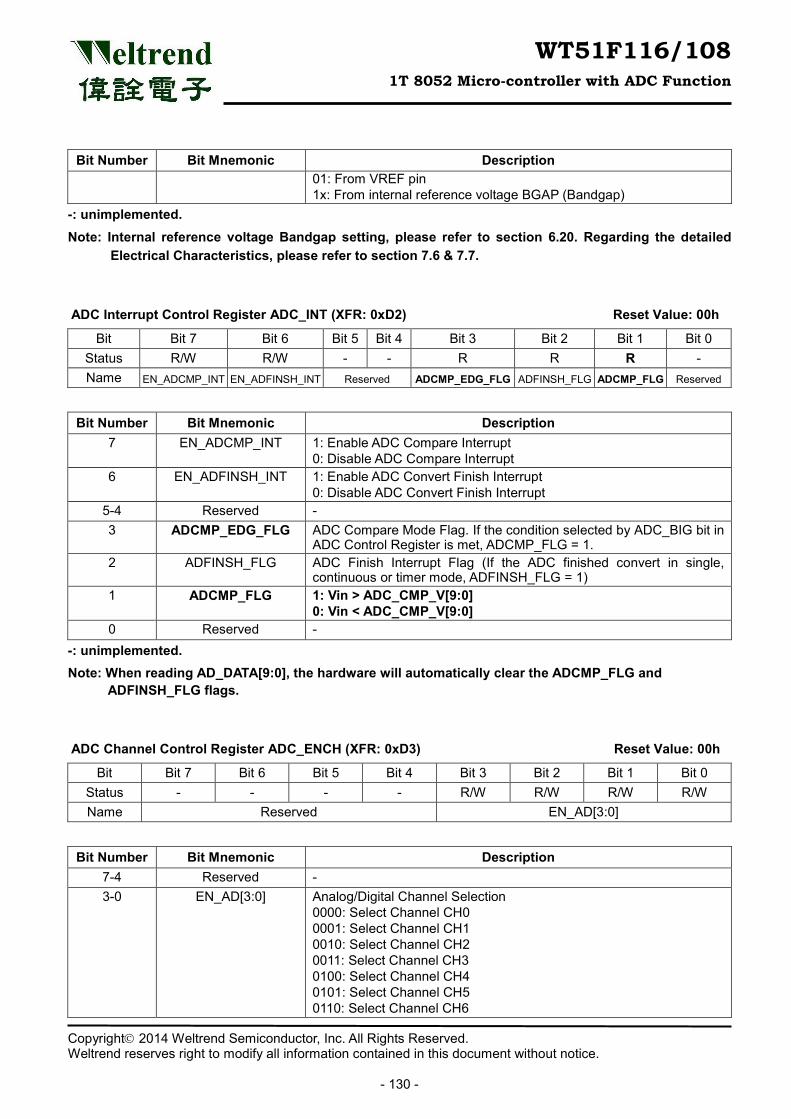
WT51F116/108 1T 8052 Micro-controller with ADC Function
Copyright 2014 Weltrend Semiconductor, Inc. All Rights Reserved. Weltrend reserves right to modify all information contained in this document without notice.
- 130 -
Bit Number Bit Mnemonic Description 01: From VREF pin 1x: From internal reference voltage BGAP (Bandgap)
-: unimplemented. Note: Internal reference voltage Bandgap setting, please refer to section 6.20. Regarding the detailed
Electrical Characteristics, please refer to section 7.6 & 7.7.
ADC Interrupt Control Register ADC_INT (XFR: 0xD2) Reset Value: 00h
Bit Bit 7 Bit 6 Bit 5 Bit 4 Bit 3 Bit 2 Bit 1 Bit 0 Status R/W R/W - - R R R - Name EN_ADCMP_INT EN_ADFINSH_INT Reserved ADCMP_EDG_FLG ADFINSH_FLG ADCMP_FLG Reserved
Bit Number Bit Mnemonic Description 7 EN_ADCMP_INT 1: Enable ADC Compare Interrupt
0: Disable ADC Compare Interrupt 6 EN_ADFINSH_INT 1: Enable ADC Convert Finish Interrupt
0: Disable ADC Convert Finish Interrupt 5-4 Reserved - 3 ADCMP_EDG_FLG ADC Compare Mode Flag. If the condition selected by ADC_BIG bit in
ADC Control Register is met, ADCMP_FLG = 1. 2 ADFINSH_FLG ADC Finish Interrupt Flag (If the ADC finished convert in single,
continuous or timer mode, ADFINSH_FLG = 1) 1 ADCMP_FLG 1: Vin > ADC_CMP_V[9:0]
0: Vin < ADC_CMP_V[9:0] 0 Reserved -
-: unimplemented. Note: When reading AD_DATA[9:0], the hardware will automatically clear the ADCMP_FLG and
ADFINSH_FLG flags.
ADC Channel Control Register ADC_ENCH (XFR: 0xD3) Reset Value: 00h
Bit Bit 7 Bit 6 Bit 5 Bit 4 Bit 3 Bit 2 Bit 1 Bit 0 Status - - - - R/W R/W R/W R/W Name Reserved EN_AD[3:0]
Bit Number Bit Mnemonic Description 7-4 Reserved - 3-0 EN_AD[3:0] Analog/Digital Channel Selection
0000: Select Channel CH0 0001: Select Channel CH1 0010: Select Channel CH2 0011: Select Channel CH3 0100: Select Channel CH4 0101: Select Channel CH5 0110: Select Channel CH6
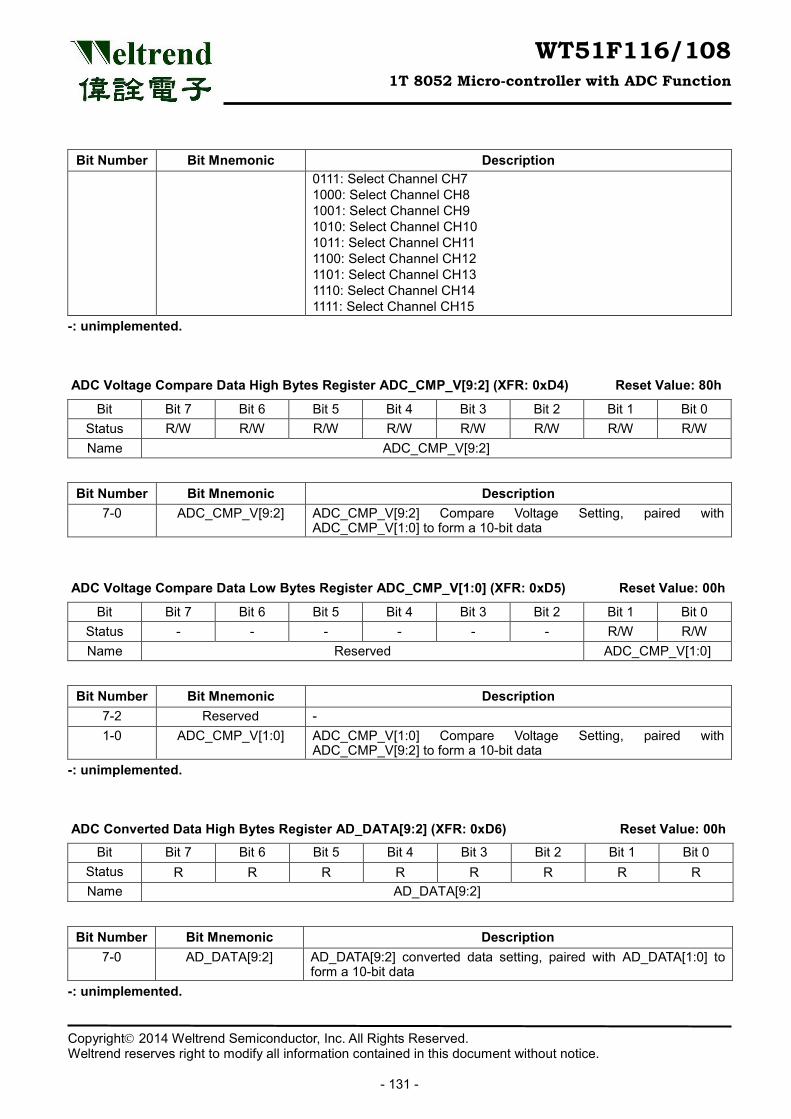
WT51F116/108 1T 8052 Micro-controller with ADC Function
Copyright 2014 Weltrend Semiconductor, Inc. All Rights Reserved. Weltrend reserves right to modify all information contained in this document without notice.
- 131 -
Bit Number Bit Mnemonic Description 0111: Select Channel CH7 1000: Select Channel CH8 1001: Select Channel CH9 1010: Select Channel CH10 1011: Select Channel CH11 1100: Select Channel CH12 1101: Select Channel CH13 1110: Select Channel CH14 1111: Select Channel CH15
-: unimplemented.
ADC Voltage Compare Data High Bytes Register ADC_CMP_V[9:2] (XFR: 0xD4) Reset Value: 80h
Bit Bit 7 Bit 6 Bit 5 Bit 4 Bit 3 Bit 2 Bit 1 Bit 0 Status R/W R/W R/W R/W R/W R/W R/W R/W Name ADC_CMP_V[9:2]
Bit Number Bit Mnemonic Description 7-0 ADC_CMP_V[9:2] ADC_CMP_V[9:2] Compare Voltage Setting, paired with
ADC_CMP_V[1:0] to form a 10-bit data
ADC Voltage Compare Data Low Bytes Register ADC_CMP_V[1:0] (XFR: 0xD5) Reset Value: 00h
Bit Bit 7 Bit 6 Bit 5 Bit 4 Bit 3 Bit 2 Bit 1 Bit 0 Status - - - - - - R/W R/W Name Reserved ADC_CMP_V[1:0]
Bit Number Bit Mnemonic Description 7-2 Reserved - 1-0 ADC_CMP_V[1:0] ADC_CMP_V[1:0] Compare Voltage Setting, paired with
ADC_CMP_V[9:2] to form a 10-bit data -: unimplemented.
ADC Converted Data High Bytes Register AD_DATA[9:2] (XFR: 0xD6) Reset Value: 00h
Bit Bit 7 Bit 6 Bit 5 Bit 4 Bit 3 Bit 2 Bit 1 Bit 0 Status R R R R R R R R Name AD_DATA[9:2]
Bit Number Bit Mnemonic Description 7-0 AD_DATA[9:2] AD_DATA[9:2] converted data setting, paired with AD_DATA[1:0] to
form a 10-bit data -: unimplemented.
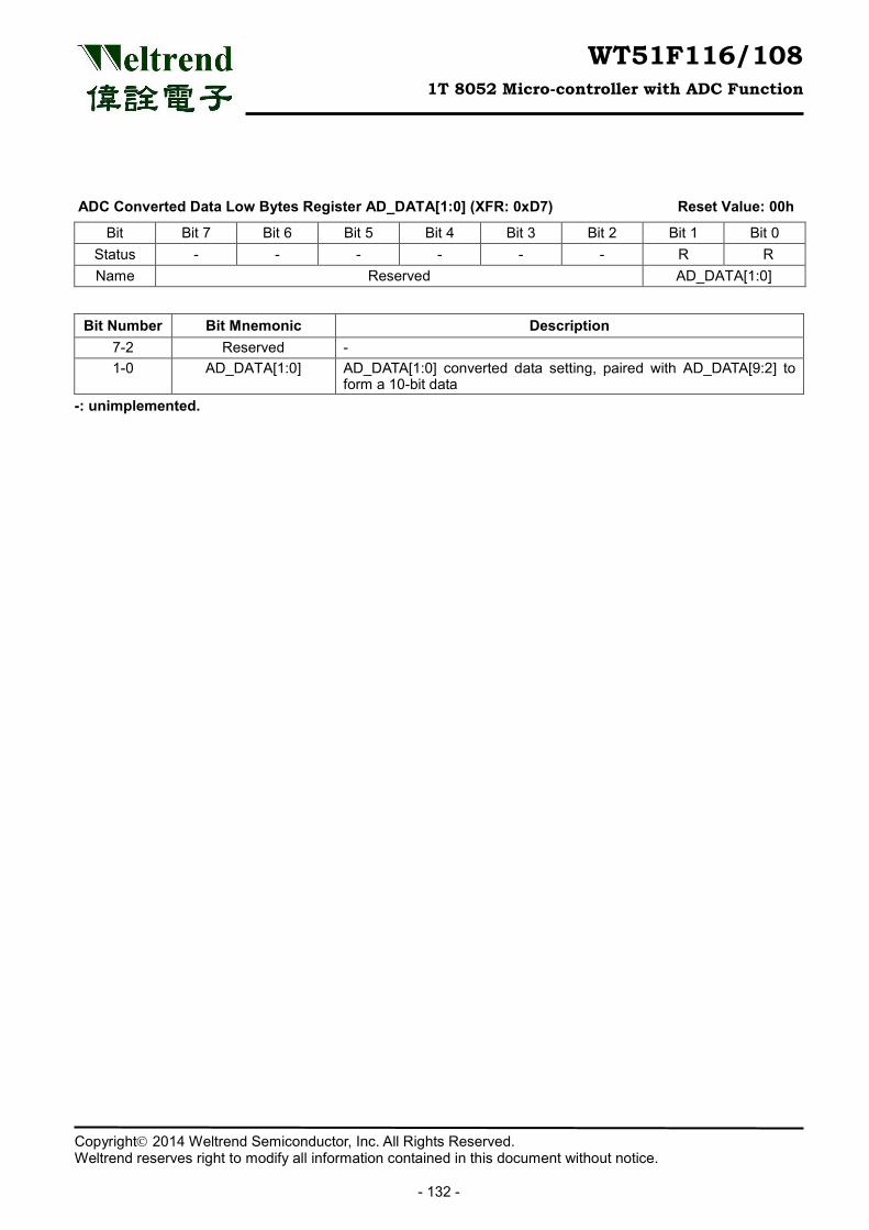
WT51F116/108 1T 8052 Micro-controller with ADC Function
Copyright 2014 Weltrend Semiconductor, Inc. All Rights Reserved. Weltrend reserves right to modify all information contained in this document without notice.
- 132 -
ADC Converted Data Low Bytes Register AD_DATA[1:0] (XFR: 0xD7) Reset Value: 00h
Bit Bit 7 Bit 6 Bit 5 Bit 4 Bit 3 Bit 2 Bit 1 Bit 0 Status - - - - - - R R Name Reserved AD_DATA[1:0]
Bit Number Bit Mnemonic Description 7-2 Reserved - 1-0 AD_DATA[1:0] AD_DATA[1:0] converted data setting, paired with AD_DATA[9:2] to
form a 10-bit data -: unimplemented.
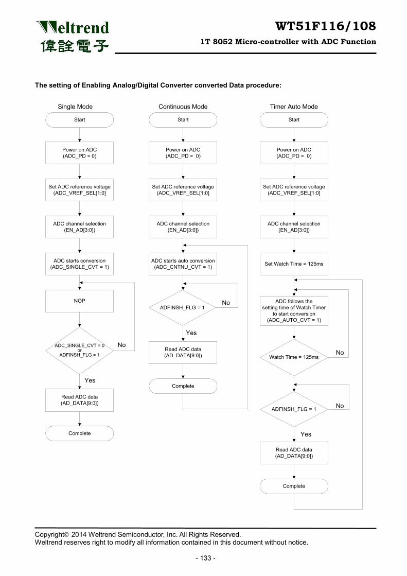
WT51F116/108 1T 8052 Micro-controller with ADC Function
Copyright 2014 Weltrend Semiconductor, Inc. All Rights Reserved. Weltrend reserves right to modify all information contained in this document without notice.
- 133 -
The setting of Enabling Analog/Digital Converter converted Data procedure:
Start
Power on ADC(ADC_PD = 0)
ADC channel selection(EN_AD[3:0])
Set ADC reference voltage(ADC_VREF_SEL[1:0]
ADC starts conversion(ADC_SINGLE_CVT = 1)
ADC_SINGLE_CVT = 0or
ADFINSH_FLG = 1
Read ADC data(AD_DATA[9:0])
NOP
No
Yes
Complete
Start
Power on ADC(ADC_PD = 0)
ADC channel selection (EN_AD[3:0])
Set ADC reference voltage(ADC_VREF_SEL[1:0]
ADC starts auto conversion(ADC_CNTNU_CVT = 1)
Read ADC data(AD_DATA[9:0])
Complete
Single Mode Continuous Mode
Start
Power on ADC(ADC_PD = 0)
ADC channel selection(EN_AD[3:0])
Set ADC reference voltage(ADC_VREF_SEL[1:0]
Watch Time = 125ms
Read ADC data(AD_DATA[9:0])
No
Yes
Complete
Timer Auto Mode
ADC follows thesetting time of Watch Timer
to start conversion(ADC_AUTO_CVT = 1)
Set Watch Time = 125ms
ADFINSH_FLG = 1No
ADFINSH_FLG = 1 No
Yes
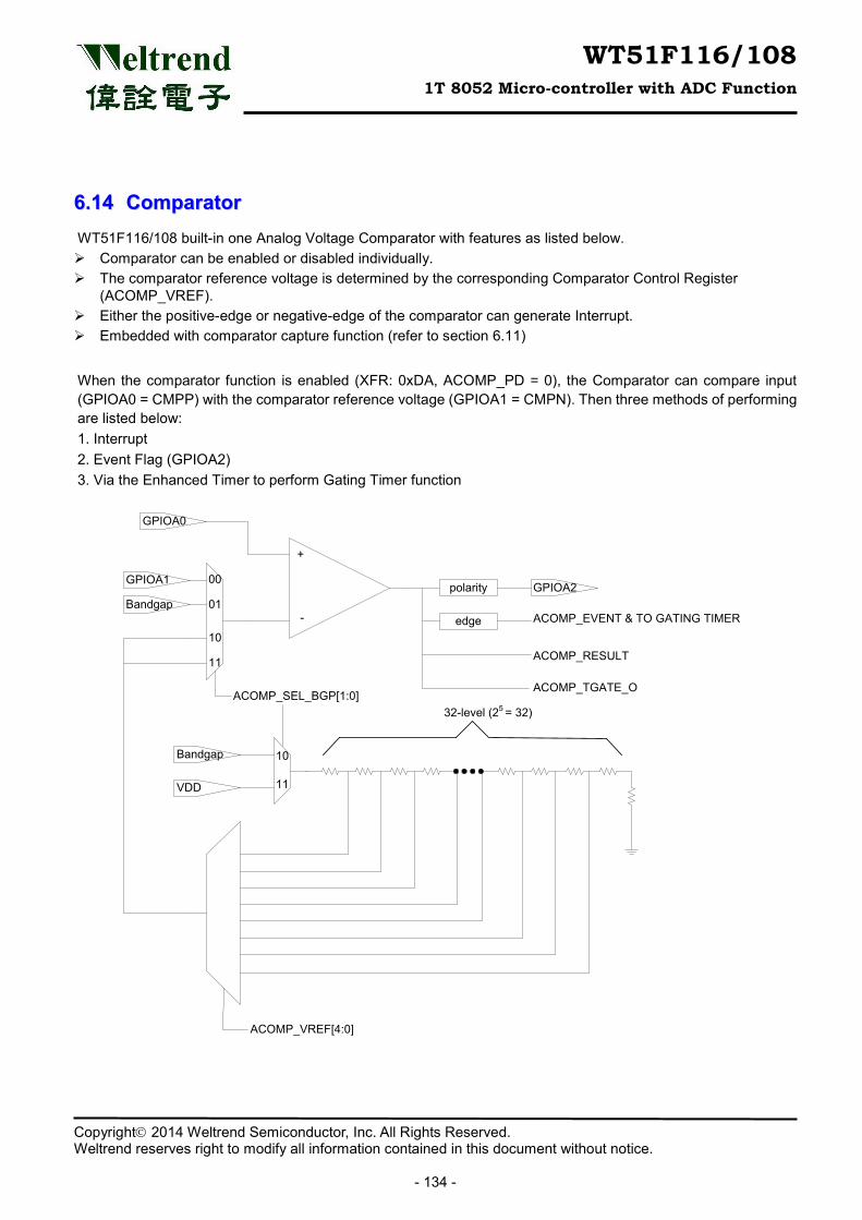
WT51F116/108 1T 8052 Micro-controller with ADC Function
Copyright 2014 Weltrend Semiconductor, Inc. All Rights Reserved. Weltrend reserves right to modify all information contained in this document without notice.
- 134 -
66..1144 CCoommppaarraattoorr WT51F116/108 built-in one Analog Voltage Comparator with features as listed below. Comparator can be enabled or disabled individually. The comparator reference voltage is determined by the corresponding Comparator Control Register
(ACOMP_VREF). Either the positive-edge or negative-edge of the comparator can generate Interrupt. Embedded with comparator capture function (refer to section 6.11) When the comparator function is enabled (XFR: 0xDA, ACOMP_PD = 0), the Comparator can compare input (GPIOA0 = CMPP) with the comparator reference voltage (GPIOA1 = CMPN). Then three methods of performing are listed below: 1. Interrupt 2. Event Flag (GPIOA2) 3. Via the Enhanced Timer to perform Gating Timer function
-
+
GPIOA1
Bandgap
00
01
10
11
Bandgap
VDD
10
11
ACOMP_SEL_BGP[1:0]
ACOMP_VREF[4:0]
GPIOA0
GPIOA2
ACOMP_EVENT & TO GATING TIMER
polarity
edge
ACOMP_RESULT
ACOMP_TGATE_O
32-level (25 = 32)
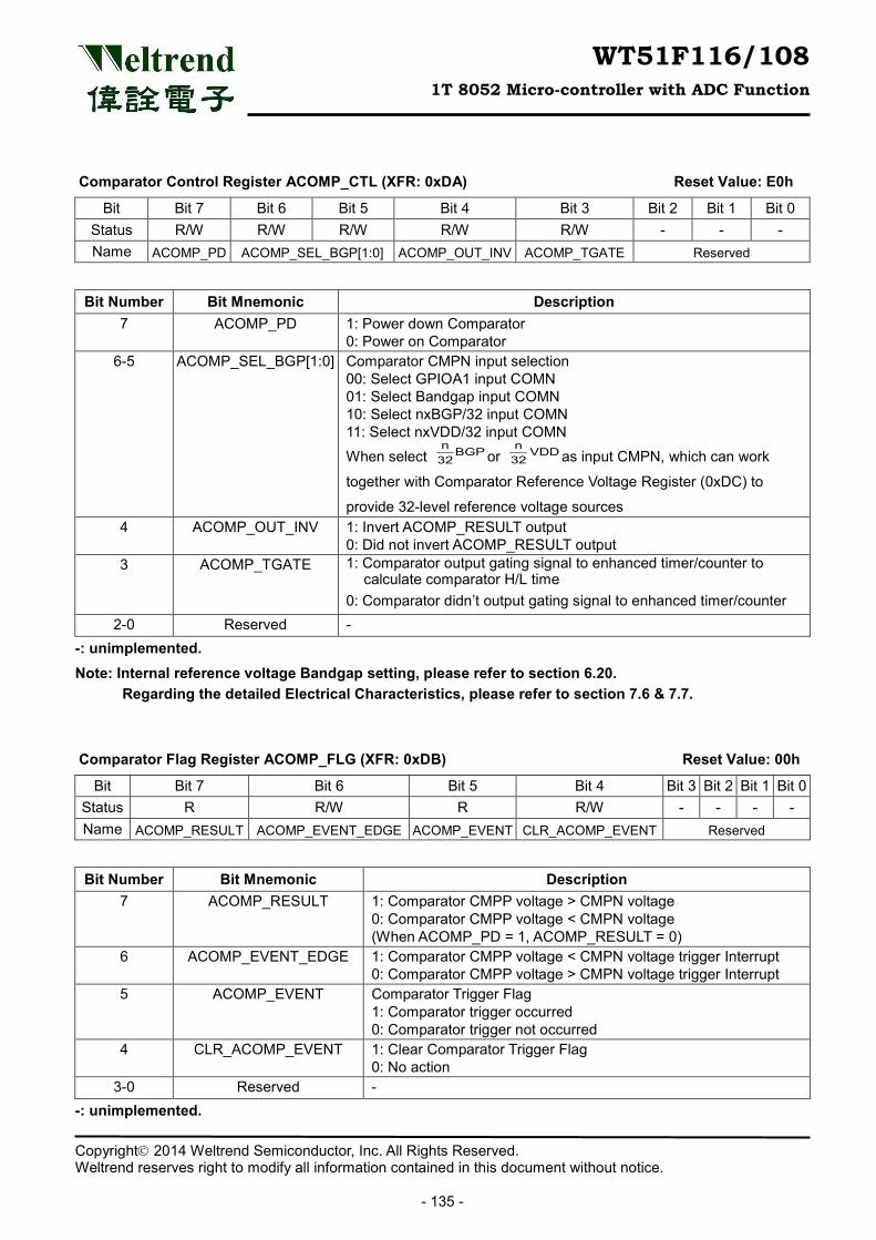
WT51F116/108 1T 8052 Micro-controller with ADC Function
Copyright 2014 Weltrend Semiconductor, Inc. All Rights Reserved. Weltrend reserves right to modify all information contained in this document without notice.
- 135 -
Comparator Control Register ACOMP_CTL (XFR: 0xDA) Reset Value: E0h
Bit Bit 7 Bit 6 Bit 5 Bit 4 Bit 3 Bit 2 Bit 1 Bit 0 Status R/W R/W R/W R/W R/W - - - Name ACOMP_PD ACOMP_SEL_BGP[1:0] ACOMP_OUT_INV ACOMP_TGATE Reserved
Bit Number Bit Mnemonic Description 7 ACOMP_PD 1: Power down Comparator
0: Power on Comparator 6-5 ACOMP_SEL_BGP[1:0] Comparator CMPN input selection
00: Select GPIOA1 input COMN 01: Select Bandgap input COMN 10: Select nxBGP/32 input COMN 11: Select nxVDD/32 input COMN
When select BGP32n
or VDD32n
as input CMPN, which can work
together with Comparator Reference Voltage Register (0xDC) to
provide 32-level reference voltage sources 4 ACOMP_OUT_INV 1: Invert ACOMP_RESULT output
0: Did not invert ACOMP_RESULT output 3 ACOMP_TGATE 1: Comparator output gating signal to enhanced timer/counter to
calculate comparator H/L time 0: Comparator didn’t output gating signal to enhanced timer/counter
2-0 Reserved - -: unimplemented. Note: Internal reference voltage Bandgap setting, please refer to section 6.20.
Regarding the detailed Electrical Characteristics, please refer to section 7.6 & 7.7.
Comparator Flag Register ACOMP_FLG (XFR: 0xDB) Reset Value: 00h
Bit Bit 7 Bit 6 Bit 5 Bit 4 Bit 3 Bit 2 Bit 1 Bit 0 Status R R/W R R/W - - - - Name ACOMP_RESULT ACOMP_EVENT_EDGE ACOMP_EVENT CLR_ACOMP_EVENT Reserved
Bit Number Bit Mnemonic Description 7 ACOMP_RESULT 1: Comparator CMPP voltage > CMPN voltage
0: Comparator CMPP voltage < CMPN voltage (When ACOMP_PD = 1, ACOMP_RESULT = 0)
6 ACOMP_EVENT_EDGE 1: Comparator CMPP voltage < CMPN voltage trigger Interrupt 0: Comparator CMPP voltage > CMPN voltage trigger Interrupt
5 ACOMP_EVENT Comparator Trigger Flag 1: Comparator trigger occurred 0: Comparator trigger not occurred
4 CLR_ACOMP_EVENT 1: Clear Comparator Trigger Flag 0: No action
3-0 Reserved - -: unimplemented.
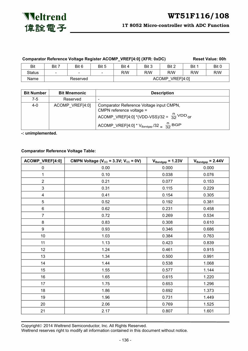
WT51F116/108 1T 8052 Micro-controller with ADC Function
Copyright 2014 Weltrend Semiconductor, Inc. All Rights Reserved. Weltrend reserves right to modify all information contained in this document without notice.
- 136 -
Comparator Reference Voltage Register ACOMP_VREF[4:0] (XFR: 0xDC) Reset Value: 00h
Bit Bit 7 Bit 6 Bit 5 Bit 4 Bit 3 Bit 2 Bit 1 Bit 0 Status - - - R/W R/W R/W R/W R/W Name Reserved ACOMP_VREF[4:0]
Bit Number Bit Mnemonic Description 7-5 Reserved - 4-0 ACOMP_VREF[4:0] Comparator Reference Voltage input CMPN,
CMPN reference voltage = ACOMP_VREF[4:0] *(VDD-VSS)/32 = VDD
32n
or ACOMP_VREF[4:0] * VBandgap /32 = BGP
32n
-: unimplemented.
Comparator Reference Voltage Table:
ACOMP_VREF[4:0] CMPN Voltage (VDD = 3.3V; VSS = 0V) VBandgap = 1.23V VBandgap = 2.44V 0 0.00 0.000 0.000 1 0.10 0.038 0.076 2 0.21 0.077 0.153 3 0.31 0.115 0.229 4 0.41 0.154 0.305 5 0.52 0.192 0.381 6 0.62 0.231 0.458 7 0.72 0.269 0.534 8 0.83 0.308 0.610 9 0.93 0.346 0.686 10 1.03 0.384 0.763 11 1.13 0.423 0.839 12 1.24 0.461 0.915 13 1.34 0.500 0.991 14 1.44 0.538 1.068 15 1.55 0.577 1.144 16 1.65 0.615 1.220 17 1.75 0.653 1.296 18 1.86 0.692 1.373 19 1.96 0.731 1.449 20 2.06 0.769 1.525 21 2.17 0.807 1.601
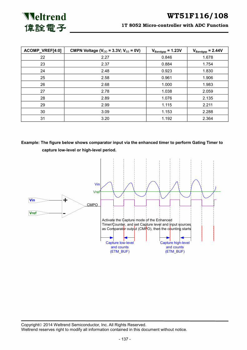
WT51F116/108 1T 8052 Micro-controller with ADC Function
Copyright 2014 Weltrend Semiconductor, Inc. All Rights Reserved. Weltrend reserves right to modify all information contained in this document without notice.
- 137 -
ACOMP_VREF[4:0] CMPN Voltage (VDD = 3.3V; VSS = 0V) VBandgap = 1.23V VBandgap = 2.44V 22 2.27 0.846 1.678 23 2.37 0.884 1.754 24 2.48 0.923 1.830 25 2.58 0.961 1.906 26 2.68 1.000 1.983 27 2.78 1.038 2.059 28 2.89 1.076 2.135 29 2.99 1.115 2.211 30 3.09 1.153 2.288 31 3.20 1.192 2.364
Example: The figure below shows comparator input via the enhanced timer to perform Gating Timer to
capture low-level or high-level period.
-+Vin
Vref
CMPO
Vin
Vref
Capture low-level and counts(ETM_BUF)
Activate the Capture mode of the Enhanced Timer/Counter, and set Capture level and input sources as Comparator output (CMPO), then the counting starts
Capture high-level and counts (ETM_BUF)
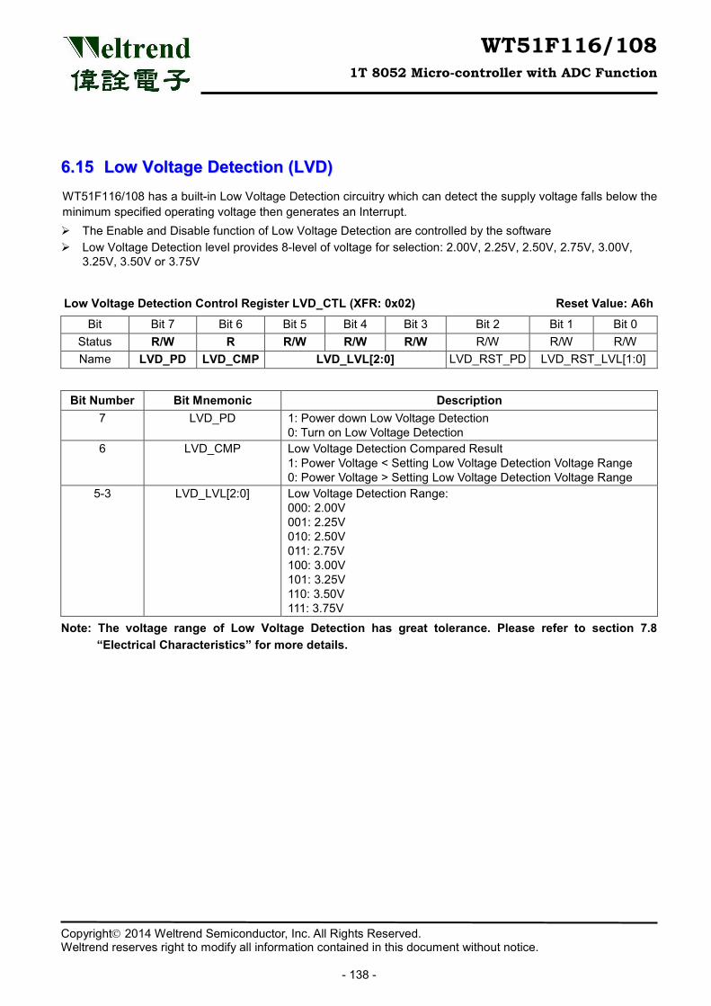
WT51F116/108 1T 8052 Micro-controller with ADC Function
Copyright 2014 Weltrend Semiconductor, Inc. All Rights Reserved. Weltrend reserves right to modify all information contained in this document without notice.
- 138 -
66..1155 LLooww VVoollttaaggee DDeetteeccttiioonn ((LLVVDD)) WT51F116/108 has a built-in Low Voltage Detection circuitry which can detect the supply voltage falls below the minimum specified operating voltage then generates an Interrupt. The Enable and Disable function of Low Voltage Detection are controlled by the software Low Voltage Detection level provides 8-level of voltage for selection: 2.00V, 2.25V, 2.50V, 2.75V, 3.00V,
3.25V, 3.50V or 3.75V
Low Voltage Detection Control Register LVD_CTL (XFR: 0x02) Reset Value: A6h
Bit Bit 7 Bit 6 Bit 5 Bit 4 Bit 3 Bit 2 Bit 1 Bit 0 Status R/W R R/W R/W R/W R/W R/W R/W Name LVD_PD LVD_CMP LVD_LVL[2:0] LVD_RST_PD LVD_RST_LVL[1:0]
Bit Number Bit Mnemonic Description 7 LVD_PD 1: Power down Low Voltage Detection
0: Turn on Low Voltage Detection 6 LVD_CMP Low Voltage Detection Compared Result
1: Power Voltage < Setting Low Voltage Detection Voltage Range 0: Power Voltage > Setting Low Voltage Detection Voltage Range
5-3 LVD_LVL[2:0] Low Voltage Detection Range: 000: 2.00V 001: 2.25V 010: 2.50V 011: 2.75V 100: 3.00V 101: 3.25V 110: 3.50V 111: 3.75V
Note: The voltage range of Low Voltage Detection has great tolerance. Please refer to section 7.8 “Electrical Characteristics” for more details.
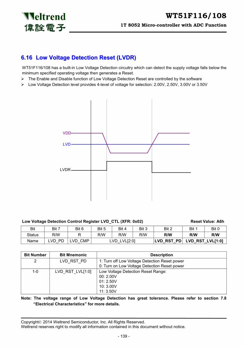
WT51F116/108 1T 8052 Micro-controller with ADC Function
Copyright 2014 Weltrend Semiconductor, Inc. All Rights Reserved. Weltrend reserves right to modify all information contained in this document without notice.
- 139 -
66..1166 LLooww VVoollttaaggee DDeetteeccttiioonn RReesseett ((LLVVDDRR)) WT51F116/108 has a built-in Low Voltage Detection circuitry which can detect the supply voltage falls below the minimum specified operating voltage then generates a Reset. The Enable and Disable function of Low Voltage Detection Reset are controlled by the software Low Voltage Detection level provides 4-level of voltage for selection: 2.00V, 2.50V, 3.00V or 3.50V
VDD
LVD
LVDR
Low Voltage Detection Control Register LVD_CTL (XFR: 0x02) Reset Value: A6h
Bit Bit 7 Bit 6 Bit 5 Bit 4 Bit 3 Bit 2 Bit 1 Bit 0 Status R/W R R/W R/W R/W R/W R/W R/W Name LVD_PD LVD_CMP LVD_LVL[2:0] LVD_RST_PD LVD_RST_LVL[1:0]
Bit Number Bit Mnemonic Description 2 LVD_RST_PD 1: Turn off Low Voltage Detection Reset power
0: Turn on Low Voltage Detection Reset power 1-0 LVD_RST_LVL[1:0] Low Voltage Detection Reset Range:
00: 2.00V 01: 2.50V 10: 3.00V 11: 3.50V
Note: The voltage range of Low Voltage Detection has great tolerance. Please refer to section 7.8 “Electrical Characteristics” for more details.
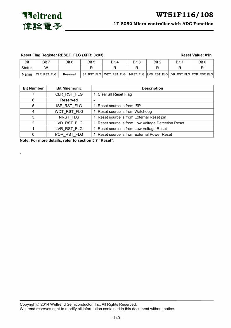
WT51F116/108 1T 8052 Micro-controller with ADC Function
Copyright 2014 Weltrend Semiconductor, Inc. All Rights Reserved. Weltrend reserves right to modify all information contained in this document without notice.
- 140 -
Reset Flag Register RESET_FLG (XFR: 0x03) Reset Value: 01h
Bit Bit 7 Bit 6 Bit 5 Bit 4 Bit 3 Bit 2 Bit 1 Bit 0 Status W - R R R R R R Name CLR_RST_FLG Reserved ISP_RST_FLG WDT_RST_FLG NRST_FLG LVD_RST_FLG LVR_RST_FLG POR_RST_FLG
Bit Number Bit Mnemonic Description 7 CLR_RST_FLG 1: Clear all Reset Flag 6 Reserved - 5 ISP_RST_FLG 1: Reset source is from ISP 4 WDT_RST_FLG 1: Reset source is from Watchdog 3 NRST_FLG 1: Reset source is from External Reset pin 2 LVD_RST_FLG 1: Reset source is from Low Voltage Detection Reset 1 LVR_RST_FLG 1: Reset source is from Low Voltage Reset 0 POR_RST_FLG 1: Reset source is from External Power Reset
Note: For more details, refer to section 5.7 “Reset”.
`
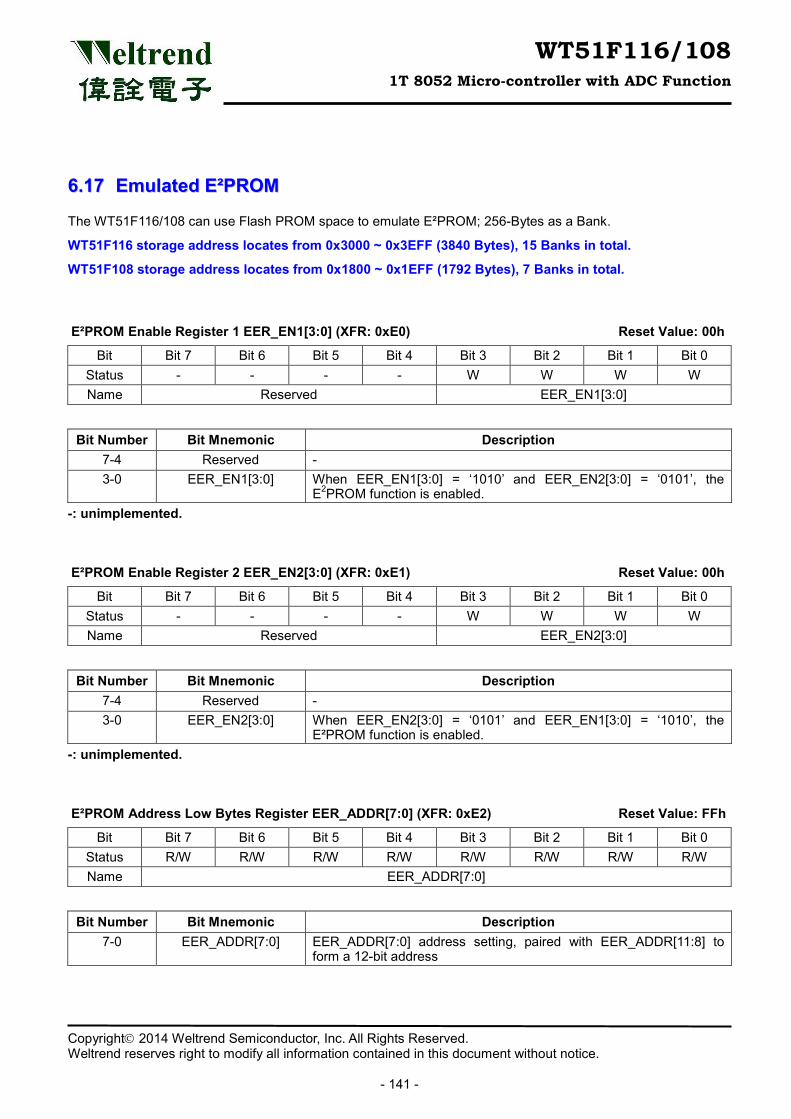
WT51F116/108 1T 8052 Micro-controller with ADC Function
Copyright 2014 Weltrend Semiconductor, Inc. All Rights Reserved. Weltrend reserves right to modify all information contained in this document without notice.
- 141 -
66..1177 EEmmuullaatteedd EE²²PPRROOMM
The WT51F116/108 can use Flash PROM space to emulate E²PROM; 256-Bytes as a Bank.
WT51F116 storage address locates from 0x3000 ~ 0x3EFF (3840 Bytes), 15 Banks in total.
WT51F108 storage address locates from 0x1800 ~ 0x1EFF (1792 Bytes), 7 Banks in total.
E²PROM Enable Register 1 EER_EN1[3:0] (XFR: 0xE0) Reset Value: 00h
Bit Bit 7 Bit 6 Bit 5 Bit 4 Bit 3 Bit 2 Bit 1 Bit 0 Status - - - - W W W W Name Reserved EER_EN1[3:0]
Bit Number Bit Mnemonic Description 7-4 Reserved - 3-0 EER_EN1[3:0] When EER_EN1[3:0] = ‘1010’ and EER_EN2[3:0] = ‘0101’, the
E2PROM function is enabled. -: unimplemented.
E²PROM Enable Register 2 EER_EN2[3:0] (XFR: 0xE1) Reset Value: 00h
Bit Bit 7 Bit 6 Bit 5 Bit 4 Bit 3 Bit 2 Bit 1 Bit 0 Status - - - - W W W W Name Reserved EER_EN2[3:0]
Bit Number Bit Mnemonic Description 7-4 Reserved - 3-0 EER_EN2[3:0] When EER_EN2[3:0] = ‘0101’ and EER_EN1[3:0] = ‘1010’, the
E²PROM function is enabled. -: unimplemented.
E²PROM Address Low Bytes Register EER_ADDR[7:0] (XFR: 0xE2) Reset Value: FFh
Bit Bit 7 Bit 6 Bit 5 Bit 4 Bit 3 Bit 2 Bit 1 Bit 0 Status R/W R/W R/W R/W R/W R/W R/W R/W Name EER_ADDR[7:0]
Bit Number Bit Mnemonic Description 7-0 EER_ADDR[7:0] EER_ADDR[7:0] address setting, paired with EER_ADDR[11:8] to
form a 12-bit address
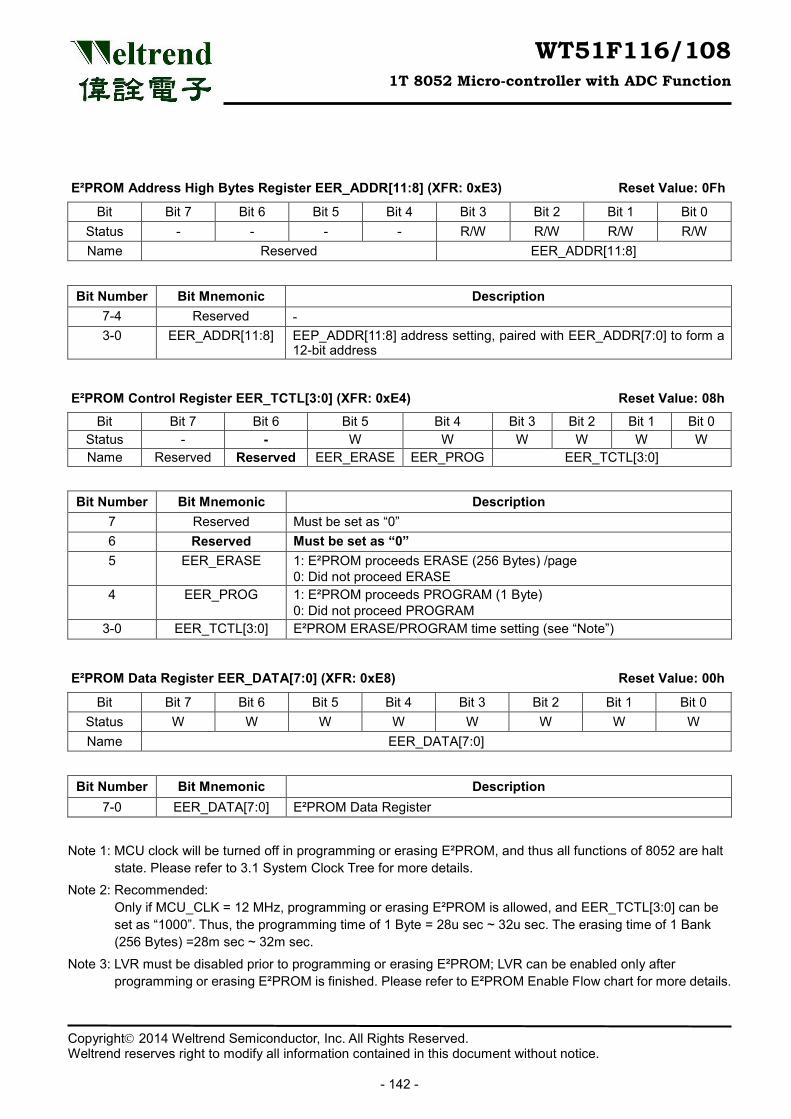
WT51F116/108 1T 8052 Micro-controller with ADC Function
Copyright 2014 Weltrend Semiconductor, Inc. All Rights Reserved. Weltrend reserves right to modify all information contained in this document without notice.
- 142 -
E²PROM Address High Bytes Register EER_ADDR[11:8] (XFR: 0xE3) Reset Value: 0Fh
Bit Bit 7 Bit 6 Bit 5 Bit 4 Bit 3 Bit 2 Bit 1 Bit 0 Status - - - - R/W R/W R/W R/W Name Reserved EER_ADDR[11:8]
Bit Number Bit Mnemonic Description 7-4 Reserved - 3-0 EER_ADDR[11:8] EEP_ADDR[11:8] address setting, paired with EER_ADDR[7:0] to form a
12-bit address
E²PROM Control Register EER_TCTL[3:0] (XFR: 0xE4) Reset Value: 08h
Bit Bit 7 Bit 6 Bit 5 Bit 4 Bit 3 Bit 2 Bit 1 Bit 0 Status - - W W W W W W Name Reserved Reserved EER_ERASE EER_PROG EER_TCTL[3:0]
Bit Number Bit Mnemonic Description 7 Reserved Must be set as “0” 6 Reserved Must be set as “0” 5 EER_ERASE 1: E²PROM proceeds ERASE (256 Bytes) /page
0: Did not proceed ERASE 4 EER_PROG 1: E²PROM proceeds PROGRAM (1 Byte)
0: Did not proceed PROGRAM 3-0 EER_TCTL[3:0] E²PROM ERASE/PROGRAM time setting (see “Note”)
E²PROM Data Register EER_DATA[7:0] (XFR: 0xE8) Reset Value: 00h
Bit Bit 7 Bit 6 Bit 5 Bit 4 Bit 3 Bit 2 Bit 1 Bit 0 Status W W W W W W W W Name EER_DATA[7:0]
Bit Number Bit Mnemonic Description 7-0 EER_DATA[7:0] E²PROM Data Register
Note 1: MCU clock will be turned off in programming or erasing E²PROM, and thus all functions of 8052 are halt
state. Please refer to 3.1 System Clock Tree for more details. Note 2: Recommended:
Only if MCU_CLK = 12 MHz, programming or erasing E²PROM is allowed, and EER_TCTL[3:0] can be set as “1000”. Thus, the programming time of 1 Byte = 28u sec ~ 32u sec. The erasing time of 1 Bank (256 Bytes) =28m sec ~ 32m sec.
Note 3: LVR must be disabled prior to programming or erasing E²PROM; LVR can be enabled only after programming or erasing E²PROM is finished. Please refer to E²PROM Enable Flow chart for more details.
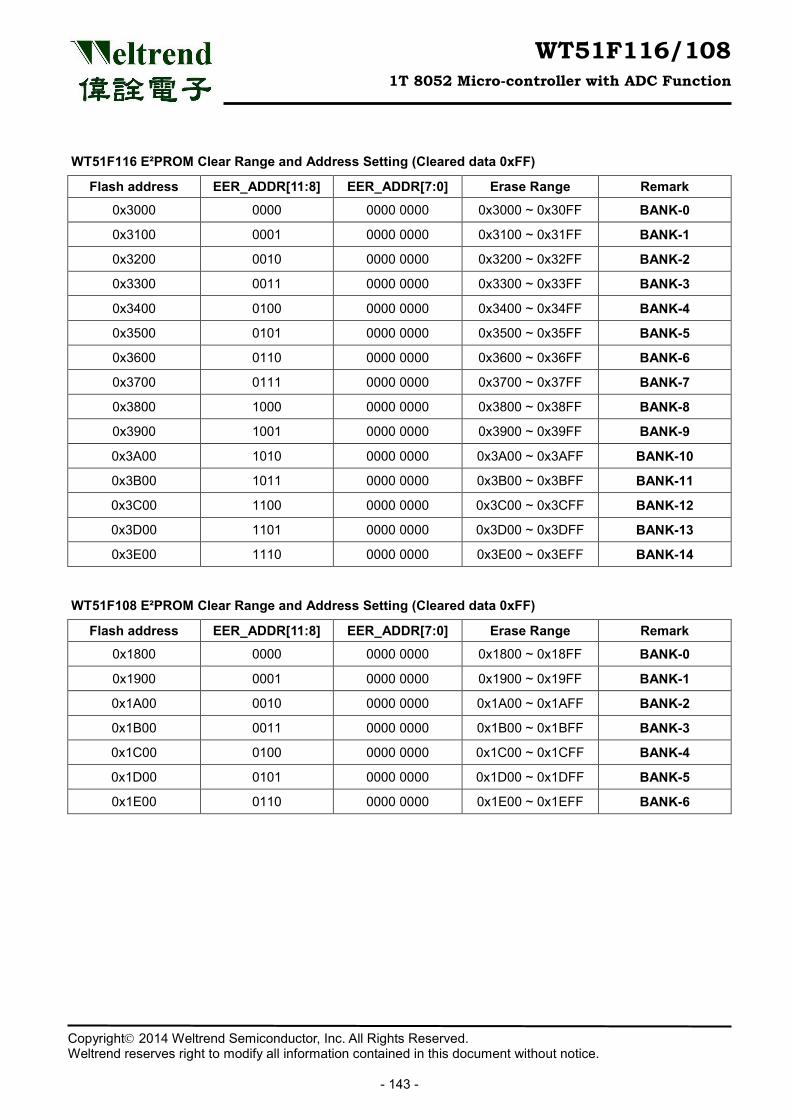
WT51F116/108 1T 8052 Micro-controller with ADC Function
Copyright 2014 Weltrend Semiconductor, Inc. All Rights Reserved. Weltrend reserves right to modify all information contained in this document without notice.
- 143 -
WT51F116 E²PROM Clear Range and Address Setting (Cleared data 0xFF)
Flash address EER_ADDR[11:8] EER_ADDR[7:0] Erase Range Remark
0x3000 0000 0000 0000 0x3000 ~ 0x30FF BANK-0
0x3100 0001 0000 0000 0x3100 ~ 0x31FF BANK-1
0x3200 0010 0000 0000 0x3200 ~ 0x32FF BANK-2
0x3300 0011 0000 0000 0x3300 ~ 0x33FF BANK-3
0x3400 0100 0000 0000 0x3400 ~ 0x34FF BANK-4
0x3500 0101 0000 0000 0x3500 ~ 0x35FF BANK-5
0x3600 0110 0000 0000 0x3600 ~ 0x36FF BANK-6
0x3700 0111 0000 0000 0x3700 ~ 0x37FF BANK-7
0x3800 1000 0000 0000 0x3800 ~ 0x38FF BANK-8
0x3900 1001 0000 0000 0x3900 ~ 0x39FF BANK-9
0x3A00 1010 0000 0000 0x3A00 ~ 0x3AFF BANK-10
0x3B00 1011 0000 0000 0x3B00 ~ 0x3BFF BANK-11
0x3C00 1100 0000 0000 0x3C00 ~ 0x3CFF BANK-12
0x3D00 1101 0000 0000 0x3D00 ~ 0x3DFF BANK-13
0x3E00 1110 0000 0000 0x3E00 ~ 0x3EFF BANK-14
WT51F108 E²PROM Clear Range and Address Setting (Cleared data 0xFF)
Flash address EER_ADDR[11:8] EER_ADDR[7:0] Erase Range Remark
0x1800 0000 0000 0000 0x1800 ~ 0x18FF BANK-0
0x1900 0001 0000 0000 0x1900 ~ 0x19FF BANK-1
0x1A00 0010 0000 0000 0x1A00 ~ 0x1AFF BANK-2
0x1B00 0011 0000 0000 0x1B00 ~ 0x1BFF BANK-3
0x1C00 0100 0000 0000 0x1C00 ~ 0x1CFF BANK-4
0x1D00 0101 0000 0000 0x1D00 ~ 0x1DFF BANK-5
0x1E00 0110 0000 0000 0x1E00 ~ 0x1EFF BANK-6
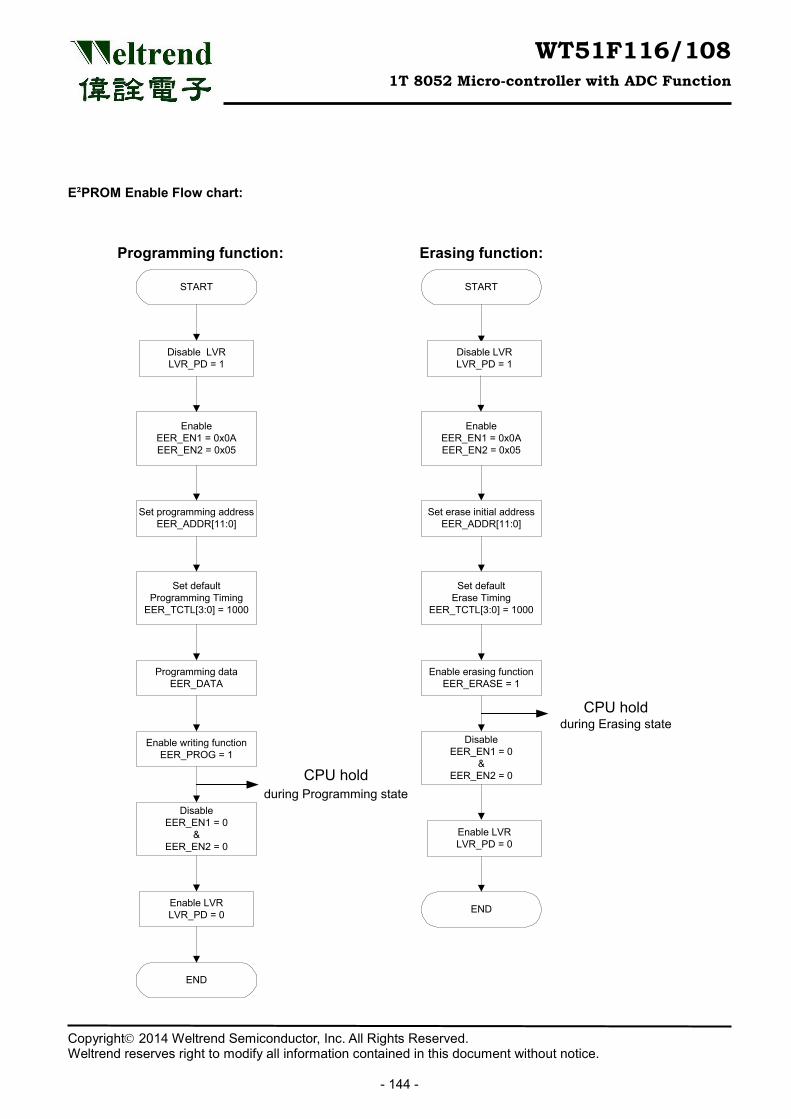
WT51F116/108 1T 8052 Micro-controller with ADC Function
Copyright 2014 Weltrend Semiconductor, Inc. All Rights Reserved. Weltrend reserves right to modify all information contained in this document without notice.
- 144 -
E²PROM Enable Flow chart:
START
EnableEER_EN1 = 0x0AEER_EN2 = 0x05
Set programming addressEER_ADDR[11:0]
Set defaultProgramming Timing
EER_TCTL[3:0] = 1000
Programming data EER_DATA
Enable writing functionEER_PROG = 1
DisableEER_EN1 = 0
&EER_EN2 = 0
END
START
Set erase initial addressEER_ADDR[11:0]
Set defaultErase Timing
EER_TCTL[3:0] = 1000
Enable erasing functionEER_ERASE = 1
DisableEER_EN1 = 0
&EER_EN2 = 0
END
CPU hold during Programming state
CPU holdduring Erasing state
Programming function: Erasing function:
EnableEER_EN1 = 0x0AEER_EN2 = 0x05
Disable LVRLVR_PD = 1
Disable LVRLVR_PD = 1
Enable LVRLVR_PD = 0
Enable LVRLVR_PD = 0
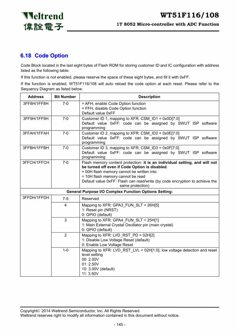
WT51F116/108 1T 8052 Micro-controller with ADC Function
Copyright 2014 Weltrend Semiconductor, Inc. All Rights Reserved. Weltrend reserves right to modify all information contained in this document without notice.
- 145 -
66..1188 CCooddee OOppttiioonn Code Block located in the last eight bytes of Flash ROM for storing customer ID and IC configuration with address listed as the following table.
If this function is not enabled, please reserve the space of these eight bytes, and fill it with 0xFF. If the function is enabled, WT51F116/108 will auto reload the code option at each reset. Please refer to the Sequency Diagram as listed below.
Address Bit Number Description 3FF8H/1FF8H 7-0 = AFH, enable Code Option function
= FFH, disable Code Option function Default value 0xFF
3FF9H/1FF9H 7-0 Customer ID 1, mapping to XFR: CSM_ID1 = 0x0D[7:0] Default value 0xFF: code can be assigned by SWUT ISP software programming
3FFAH/1FFAH 7-0 Customer ID 2, mapping to XFR: CSM_ID2 = 0x0E[7:0] Default value 0xFF: code can be assigned by SWUT ISP software programming
3FFBH/1FFBH 7-0 Customer ID 3, mapping to XFR: CSM_ID3 = 0x0F[7:0] Default value 0xFF: code can be assigned by SWUT ISP software programming
3FFCH/1FFCH 7-0 Flash memory content protection: it is an individual setting, and will not be turned off even if Code Option is disabled. = 00H flash memory cannot be written into = 10H flash memory cannot be read Default value 0xFF: Flash can read/write (by code encryption to achieve the
same protection) General Purpose I/O Complex Function Options Setting:
3FFDH/1FFDH 7-5 Reserved 4 Mapping to XFR: GPA3_FUN_SLT = 26H[5]
1: Reset pin (NRST) 0: GPIO (default)
3 Mapping to XFR: GPA4_FUN_SLT = 25H[1] 1: Main External Crystal Oscillator pin (main crystal) 0: GPIO (default)
2 Mapping to XFR: LVD_RST_PD = 02H[2] 1: Disable Low Voltage Reset (default) 0: Enable Low Voltage Reset
1-0 Mapping to XFR: LVD_RST_LVL = 02H[1:0], low voltage detection and reset level setting 00: 2.00V 01: 2.50V 10: 3.00V (default) 11: 3.50V
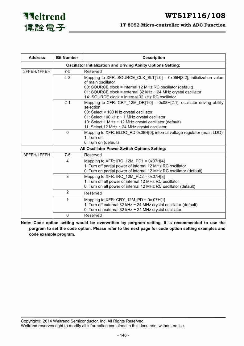
WT51F116/108 1T 8052 Micro-controller with ADC Function
Copyright 2014 Weltrend Semiconductor, Inc. All Rights Reserved. Weltrend reserves right to modify all information contained in this document without notice.
- 146 -
Address Bit Number Description
Oscillator Initialization and Driving Ability Options Setting: 3FFEH/1FFEH 7-5 Reserved
4-3 Mapping to XFR: SOURCE_CLK_SLT[1:0] = 0x05H[3:2]; initialization value of main oscillator 00: SOURCE clock = internal 12 MHz RC oscillator (default) 01: SOURCE clock = external 32 kHz ~ 24 MHz crystal oscillator 1X: SOURCE clock = internal 32 kHz RC oscillator
2-1 Mapping to XFR: CRY_12M_DR[1:0] = 0x08H[2:1]; oscillator driving ability selection 00: Select < 100 kHz crystal oscillator 01: Select 100 kHz ~ 1 MHz crystal oscillator 10: Select 1 MHz ~ 12 MHz crystal oscillator (default) 11: Select 12 MHz ~ 24 MHz crystal oscillator
0 Mapping to XFR: BLDO_PD 0x08H[0]; internal voltage regulator (main LDO) 1: Turn off 0: Turn on (default)
All Oscillator Power Switch Options Setting: 3FFFH/1FFFH
7-5 Reserved 4 Mapping to XFR: IRC_12M_PD1 = 0x07H[4]
1: Turn off partial power of internal 12 MHz RC oscillator 0: Turn on partial power of internal 12 MHz RC oscillator (default)
3 Mapping to XFR: IRC_12M_PD2 = 0x07H[3] 1: Turn off all power of internal 12 MHz RC oscillator 0: Turn on all power of internal 12 MHz RC oscillator (default)
2 Reserved 1 Mapping to XFR: CRY_12M_PD = 0x 07H[1]
1: Turn off external 32 kHz ~ 24 MHz crystal oscillator (default) 0: Turn on external 32 kHz ~ 24 MHz crystal oscillator
0 Reserved
Note: Code option setting would be overwritten by porgram setting, it is recommended to use the porgram to set the code option. Please refer to the next page for code option setting examples and code example program.
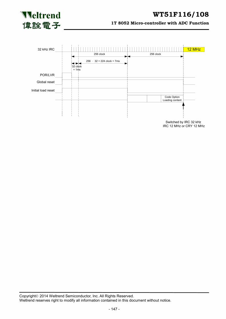
WT51F116/108 1T 8052 Micro-controller with ADC Function
Copyright 2014 Weltrend Semiconductor, Inc. All Rights Reserved. Weltrend reserves right to modify all information contained in this document without notice.
- 147 -
POR/LVR
Switched by IRC 32 kHz IRC 12 MHz or CRY 12 MHz
256 clock256 clock
256 – 32 = 224 clock = 7ms
32 clock = 1ms
Global reset
Initial load reset
32 kHz IRC 12 MHz
Code OptionLoading content
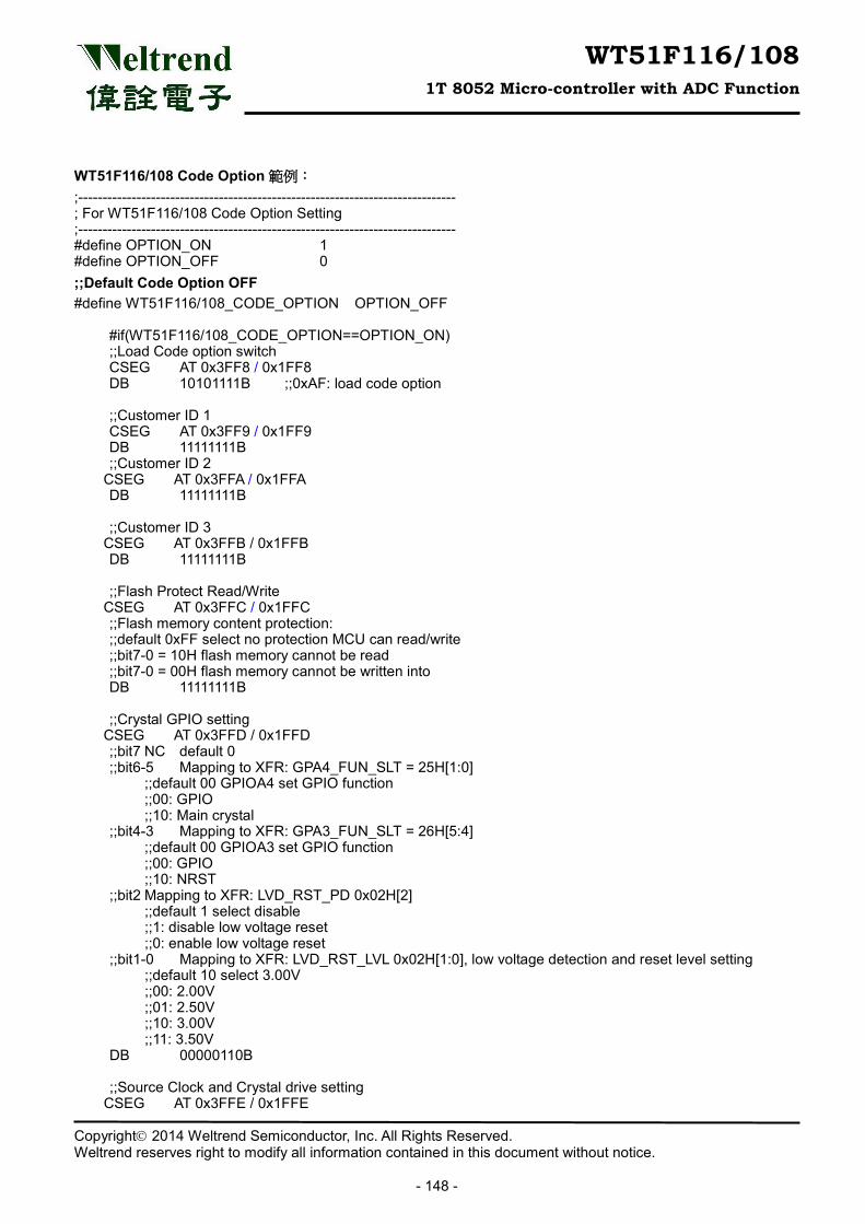
WT51F116/108 1T 8052 Micro-controller with ADC Function
Copyright 2014 Weltrend Semiconductor, Inc. All Rights Reserved. Weltrend reserves right to modify all information contained in this document without notice.
- 148 -
WT51F116/108 Code Option 範例: ;------------------------------------------------------------------------------ ; For WT51F116/108 Code Option Setting ;------------------------------------------------------------------------------ #define OPTION_ON 1 #define OPTION_OFF 0 ;;Default Code Option OFF #define WT51F116/108_CODE_OPTION OPTION_OFF #if(WT51F116/108_CODE_OPTION==OPTION_ON) ;;Load Code option switch CSEG AT 0x3FF8 / 0x1FF8 DB 10101111B ;;0xAF: load code option ;;Customer ID 1 CSEG AT 0x3FF9 / 0x1FF9 DB 11111111B ;;Customer ID 2 CSEG AT 0x3FFA / 0x1FFA DB 11111111B ;;Customer ID 3 CSEG AT 0x3FFB / 0x1FFB DB 11111111B ;;Flash Protect Read/Write CSEG AT 0x3FFC / 0x1FFC ;;Flash memory content protection: ;;default 0xFF select no protection MCU can read/write ;;bit7-0 = 10H flash memory cannot be read ;;bit7-0 = 00H flash memory cannot be written into DB 11111111B ;;Crystal GPIO setting CSEG AT 0x3FFD / 0x1FFD ;;bit7 NC default 0 ;;bit6-5 Mapping to XFR: GPA4_FUN_SLT = 25H[1:0] ;;default 00 GPIOA4 set GPIO function ;;00: GPIO ;;10: Main crystal ;;bit4-3 Mapping to XFR: GPA3_FUN_SLT = 26H[5:4] ;;default 00 GPIOA3 set GPIO function ;;00: GPIO ;;10: NRST ;;bit2 Mapping to XFR: LVD_RST_PD 0x02H[2] ;;default 1 select disable ;;1: disable low voltage reset ;;0: enable low voltage reset ;;bit1-0 Mapping to XFR: LVD_RST_LVL 0x02H[1:0], low voltage detection and reset level setting ;;default 10 select 3.00V ;;00: 2.00V ;;01: 2.50V ;;10: 3.00V ;;11: 3.50V DB 00000110B ;;Source Clock and Crystal drive setting CSEG AT 0x3FFE / 0x1FFE
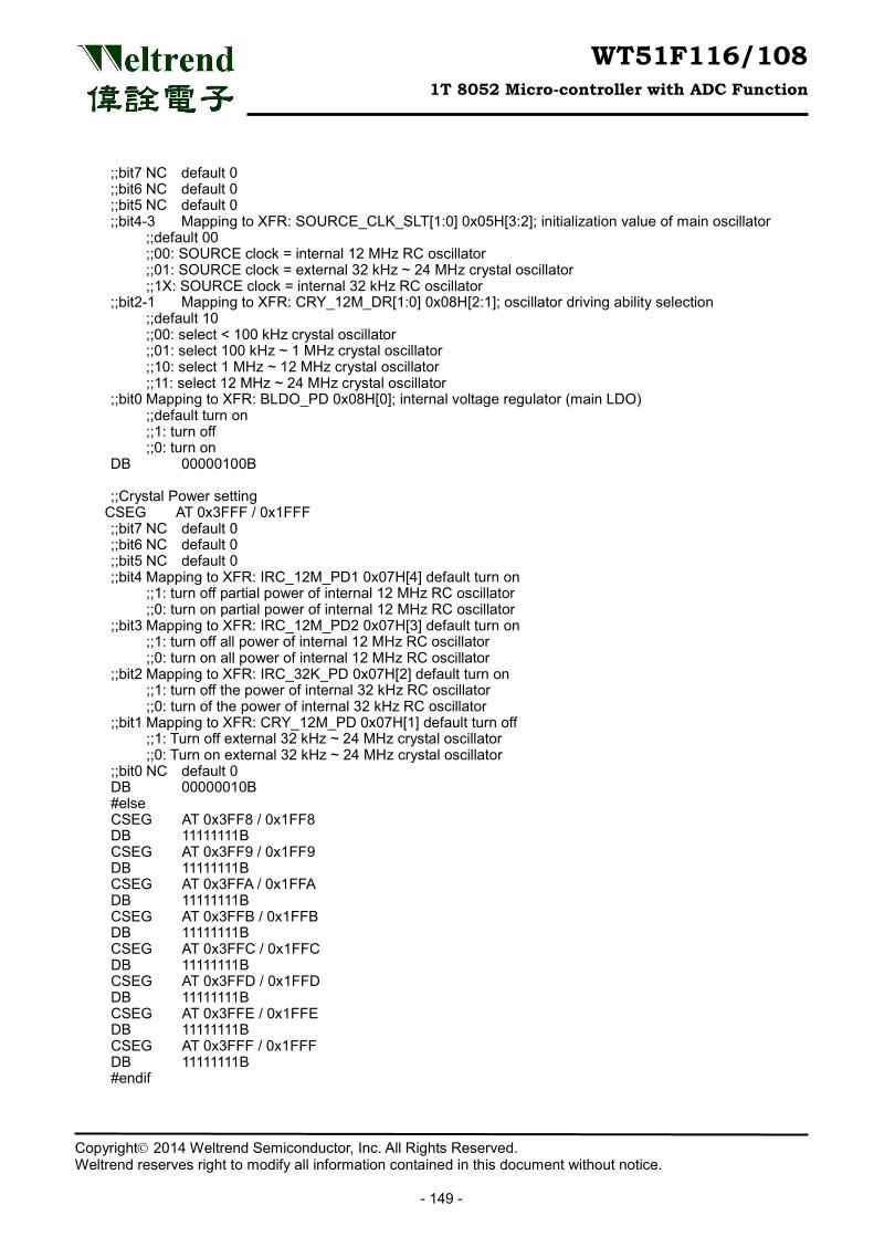
WT51F116/108 1T 8052 Micro-controller with ADC Function
Copyright 2014 Weltrend Semiconductor, Inc. All Rights Reserved. Weltrend reserves right to modify all information contained in this document without notice.
- 149 -
;;bit7 NC default 0 ;;bit6 NC default 0 ;;bit5 NC default 0 ;;bit4-3 Mapping to XFR: SOURCE_CLK_SLT[1:0] 0x05H[3:2]; initialization value of main oscillator ;;default 00 ;;00: SOURCE clock = internal 12 MHz RC oscillator ;;01: SOURCE clock = external 32 kHz ~ 24 MHz crystal oscillator ;;1X: SOURCE clock = internal 32 kHz RC oscillator ;;bit2-1 Mapping to XFR: CRY_12M_DR[1:0] 0x08H[2:1]; oscillator driving ability selection ;;default 10 ;;00: select < 100 kHz crystal oscillator ;;01: select 100 kHz ~ 1 MHz crystal oscillator ;;10: select 1 MHz ~ 12 MHz crystal oscillator ;;11: select 12 MHz ~ 24 MHz crystal oscillator ;;bit0 Mapping to XFR: BLDO_PD 0x08H[0]; internal voltage regulator (main LDO) ;;default turn on ;;1: turn off ;;0: turn on DB 00000100B ;;Crystal Power setting CSEG AT 0x3FFF / 0x1FFF ;;bit7 NC default 0 ;;bit6 NC default 0 ;;bit5 NC default 0 ;;bit4 Mapping to XFR: IRC_12M_PD1 0x07H[4] default turn on ;;1: turn off partial power of internal 12 MHz RC oscillator ;;0: turn on partial power of internal 12 MHz RC oscillator ;;bit3 Mapping to XFR: IRC_12M_PD2 0x07H[3] default turn on ;;1: turn off all power of internal 12 MHz RC oscillator ;;0: turn on all power of internal 12 MHz RC oscillator ;;bit2 Mapping to XFR: IRC_32K_PD 0x07H[2] default turn on ;;1: turn off the power of internal 32 kHz RC oscillator ;;0: turn of the power of internal 32 kHz RC oscillator ;;bit1 Mapping to XFR: CRY_12M_PD 0x07H[1] default turn off ;;1: Turn off external 32 kHz ~ 24 MHz crystal oscillator ;;0: Turn on external 32 kHz ~ 24 MHz crystal oscillator ;;bit0 NC default 0 DB 00000010B #else CSEG AT 0x3FF8 / 0x1FF8 DB 11111111B CSEG AT 0x3FF9 / 0x1FF9 DB 11111111B CSEG AT 0x3FFA / 0x1FFA DB 11111111B CSEG AT 0x3FFB / 0x1FFB DB 11111111B CSEG AT 0x3FFC / 0x1FFC DB 11111111B CSEG AT 0x3FFD / 0x1FFD DB 11111111B CSEG AT 0x3FFE / 0x1FFE DB 11111111B CSEG AT 0x3FFF / 0x1FFF DB 11111111B #endif
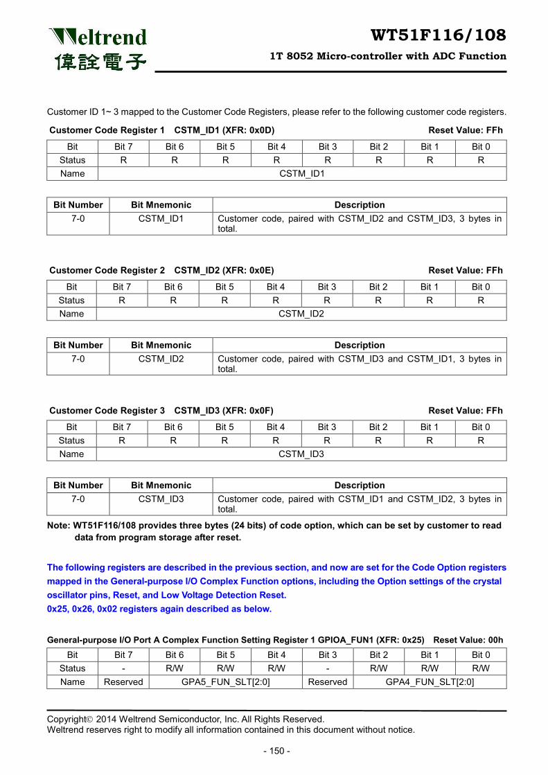
WT51F116/108 1T 8052 Micro-controller with ADC Function
Copyright 2014 Weltrend Semiconductor, Inc. All Rights Reserved. Weltrend reserves right to modify all information contained in this document without notice.
- 150 -
Customer ID 1~ 3 mapped to the Customer Code Registers, please refer to the following customer code registers.
Customer Code Register 1 CSTM_ID1 (XFR: 0x0D) Reset Value: FFh
Bit Bit 7 Bit 6 Bit 5 Bit 4 Bit 3 Bit 2 Bit 1 Bit 0 Status R R R R R R R R Name CSTM_ID1
Bit Number Bit Mnemonic Description 7-0 CSTM_ID1 Customer code, paired with CSTM_ID2 and CSTM_ID3, 3 bytes in
total.
Customer Code Register 2 CSTM_ID2 (XFR: 0x0E) Reset Value: FFh
Bit Bit 7 Bit 6 Bit 5 Bit 4 Bit 3 Bit 2 Bit 1 Bit 0 Status R R R R R R R R Name CSTM_ID2
Bit Number Bit Mnemonic Description 7-0 CSTM_ID2 Customer code, paired with CSTM_ID3 and CSTM_ID1, 3 bytes in
total.
Customer Code Register 3 CSTM_ID3 (XFR: 0x0F) Reset Value: FFh
Bit Bit 7 Bit 6 Bit 5 Bit 4 Bit 3 Bit 2 Bit 1 Bit 0 Status R R R R R R R R Name CSTM_ID3
Bit Number Bit Mnemonic Description 7-0 CSTM_ID3 Customer code, paired with CSTM_ID1 and CSTM_ID2, 3 bytes in
total.
Note: WT51F116/108 provides three bytes (24 bits) of code option, which can be set by customer to read data from program storage after reset.
The following registers are described in the previous section, and now are set for the Code Option registers mapped in the General-purpose I/O Complex Function options, including the Option settings of the crystal oscillator pins, Reset, and Low Voltage Detection Reset. 0x25, 0x26, 0x02 registers again described as below.
General-purpose I/O Port A Complex Function Setting Register 1 GPIOA_FUN1 (XFR: 0x25) Reset Value: 00h Bit Bit 7 Bit 6 Bit 5 Bit 4 Bit 3 Bit 2 Bit 1 Bit 0
Status - R/W R/W R/W - R/W R/W R/W Name Reserved GPA5_FUN_SLT[2:0] Reserved GPA4_FUN_SLT[2:0]
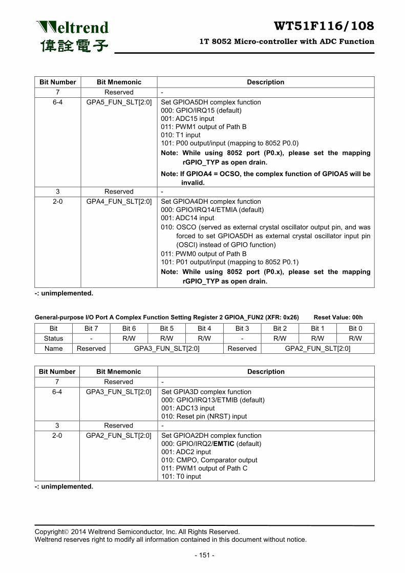
WT51F116/108 1T 8052 Micro-controller with ADC Function
Copyright 2014 Weltrend Semiconductor, Inc. All Rights Reserved. Weltrend reserves right to modify all information contained in this document without notice.
- 151 -
Bit Number Bit Mnemonic Description 7 Reserved -
6-4 GPA5_FUN_SLT[2:0] Set GPIOA5DH complex function 000: GPIO/IRQ15 (default) 001: ADC15 input 011: PWM1 output of Path B 010: T1 input 101: P00 output/input (mapping to 8052 P0.0) Note: While using 8052 port (P0.x), please set the mapping
rGPIO_TYP as open drain. Note: If GPIOA4 = OCSO, the complex function of GPIOA5 will be
invalid. 3 Reserved -
2-0 GPA4_FUN_SLT[2:0] Set GPIOA4DH complex function 000: GPIO/IRQ14/ETMIA (default) 001: ADC14 input 010: OSCO (served as external crystal oscillator output pin, and was
forced to set GPIOA5DH as external crystal oscillator input pin (OSCI) instead of GPIO function)
011: PWM0 output of Path B 101: P01 output/input (mapping to 8052 P0.1) Note: While using 8052 port (P0.x), please set the mapping
rGPIO_TYP as open drain.
-: unimplemented.
General-purpose I/O Port A Complex Function Setting Register 2 GPIOA_FUN2 (XFR: 0x26) Reset Value: 00h
Bit Bit 7 Bit 6 Bit 5 Bit 4 Bit 3 Bit 2 Bit 1 Bit 0 Status - R/W R/W R/W - R/W R/W R/W Name Reserved GPA3_FUN_SLT[2:0] Reserved GPA2_FUN_SLT[2:0]
Bit Number Bit Mnemonic Description 7 Reserved -
6-4 GPA3_FUN_SLT[2:0] Set GPIA3D complex function 000: GPIO/IRQ13/ETMIB (default) 001: ADC13 input 010: Reset pin (NRST) input
3 Reserved - 2-0 GPA2_FUN_SLT[2:0] Set GPIOA2DH complex function
000: GPIO/IRQ2/EMTIC (default) 001: ADC2 input 010: CMPO, Comparator output 011: PWM1 output of Path C 101: T0 input
-: unimplemented.
WT51F116/108 1T 8052 Micro-controller with ADC Function
Copyright 2014 Weltrend Semiconductor, Inc. All Rights Reserved. Weltrend reserves right to modify all information contained in this document without notice.
- 152 -
Low Voltage Detection Control Register LVD_CTL (XFR: 0x02) Reset Value: A6h
Bit Bit 7 Bit 6 Bit 5 Bit 4 Bit 3 Bit 2 Bit 1 Bit 0 Status R/W R R/W R/W R/W R/W R/W R/W Name LVD_PD LVD_CMP LVD_LVL[2:0] LVD_RST_PD LVD_RST_LVL[1:0]
Bit Number Bit Mnemonic Description 7 LVD_PD 1: Power down Low Voltage Detection
0: Turn on Low Voltage Detection 6 LVD_CMP Low Voltage Detection Compared Result
1: Power Voltage < Setting Low Voltage Detection Voltage Range 0: Power Voltage > Setting Low Voltage Detection Voltage Range
5-3 LVD_LVL[2:0] Low Voltage Detection Range: 000: 2.00V 001: 2.25V 010: 2.50V 011: 2.75V 100: 3.00V 101: 3.25V 110: 3.50V 111: 3.75V
The following registers is described in the previous section, and now is set for the Code Option registers mapped in the Initialized Oscillator & Driving Ability options, including the Option settings of the crystal oscillator source and Driving ability. 0x05, 0x08 Register again described as below.
System Clock Source Control Register SOURCE_CLK_SLT (XFR: 0x05) Reset Value: A0h
Bit Bit 7 Bit 6 Bit 5 Bit 4 Bit 3 Bit 2 Bit 1 Bit 0 Status - - - - R/W R/W R/W R/W Name Reserved SOURCE_CLK_SLT[1:0] MCU_CLK_SLT[1:0]
Bit Number Bit Mnemonic Description 7-4 Reserved Must be equal to ”1010”, otherwise bit [3:0] cannot be written into. 3-2 SOURCE_CLK_SLT[1:0] Select SOURCE clock sources
00: Internal 12/24 MHz RC oscillator (default) 01: External DC ~ 24 MHz crystal oscillator 10: Internal 32 kHz RC oscillator Default value can be selected by section 6.18 Code Option Select
1-0 MCU_CLK_SLT[1:0] MCU clock setting 00: MCU clock = SOURCE clock (default) 01: MCU clock = SOURCE clock /2 10: MCU clock = SOURCE clock /4 11: MCU clock = SOURCE clock /12
-: unimplemented.
WT51F116/108 1T 8052 Micro-controller with ADC Function
Copyright 2014 Weltrend Semiconductor, Inc. All Rights Reserved. Weltrend reserves right to modify all information contained in this document without notice.
- 153 -
Notes: 1. When Source clock of WT51F116 selects external 32.768 kHz crystal oscillator, BLDO_PD can be turned off to
reduce power consumption. Please select SOURCE clock as internal 32 kHz RC oscillator to work together with Watch Timer selecting external 32.768 kHz crystal oscillator.
2. When SOURCE clock selects internal 32 kHz RC oscillator and the system clock source of the Watch Timer selects External 32.768 kHz crystal oscillator, Interrupt sources cannot be captured in time due to Internal 32 kHz RC oscillator with huge tolerance and the execute speed is slower than the Interrupt generaed by Watch Timer. In this mode, it requires having the External Clock Source Prescaler Control Register 1 and External Clock Source Prescaler Control Register 2 setting divided by 2, and the Watch Timer clock source divided by 2 equals to 16.384 kHz. In the meantime, the time period selected by the Watch Timer will be extended twice to capture completely without missing.
Setting External Clock Source/ 2 procedures:
1. Setting Prescaler Data: CRY_DIV[9:0] = 1, and 32.768 kHz/(CRY_DIV[9:0]+1) = 32.768 kHz/2 =16.384 kHz
2. Enable external crystal oscillator clock source prescaler: EN_CRY_DIV = 1
Oscillator Driver Control Register CRY_12M_DR[1:0] (XFR: 0x08) Reset Value: 54h
Bit Bit 7 Bit 6 Bit 5 Bit 4 Bit 3 Bit 2 Bit 1 Bit 0 Status - - - - - R/W R/W R/W Name Reserved Reserved CRY_12M_DR[1:0] BLDO_PD
Bit Number Bit Mnemonic Description 7-4 Reserved Must be equal to ”0101”, otherwise, Bit[3:0] cannot be written into 3 Reserved -
2-1 CRY_12M_DR[1:0] External oscillator driving ability setting 00: Crystal oscillator with frequency < 100 kHz 01: Crystal oscillator with frequency of 100 kHz ~ 1 MHz 10: Crystal oscillator with frequency of 1 MHz ~ 12 MHz (default) 11: Crystal oscillator with frequency of 12 MHz ~ 24 MHz Default value can be selected by section 6.18 Code Option Select
0 BLDO_PD Internal voltage regulator (main LDO) 1: Turn off main LDO 0: Turn on main LDO (default) Default value can be selected by section 6.18 Code Option Select
-: unimplemented. Note: Main LDO is turned off only in Green mode, if SOURCE clock is IRC Internal or External crystal
oscillator then main LDO must be turned on, otherwise system may work abnormally and leads to programming failure.
WT51F116/108 1T 8052 Micro-controller with ADC Function
Copyright 2014 Weltrend Semiconductor, Inc. All Rights Reserved. Weltrend reserves right to modify all information contained in this document without notice.
- 154 -
Note: Due to WT51F116/108 only supports one set of external oscillator input, it requires setting the
driving ability of oscillator according to the frequency of external oscillator input. Please see the table below.
External Crystal Oscillator CRY_12M_DR[1:0] 24 MHz 11 12 MHz 10
32.768 kHz 00
Below Code Option setting illustrates all Oscillator Power Switch Option setting, and it is recommended to set it according to its Reset value. If you want to use an external oscillator, please wait till MCU executes procedures.
Clock Source Control Register IRC_12M_PD (XFR: 0x07) Reset Value: A2h
Bit Bit 7 Bit 6 Bit 5 Bit 4 Bit 3 Bit 2 Bit 1 Bit 0 Status - - - R/W R/W R/W R/W - Name Reserved IRC_12M_PD1 IRC_12M_PD2 IRC_32K_PD CRY_12M_PD Reserved
Bit Number Bit Mnemonic Description 7-5 - Must be equal to ”101”, otherwise bit[4:0] cannot be written into 4 IRC_12M_PD1 1: Partial internal 12/24 MHz RC oscillator power is turned off (bias
ON) (default value is not off) 0: Not off
3 IRC_12M_PD2 1: All internal 12/24 MHz RC oscillator power are turned off (bias off) (default value is not off)
0: Not off 2 IRC_32K_PD 1: Internal 32 kHz RC oscillator power is turned off (default value is not
off) 0: Not off
1 CRY_12M_PD 1: External 12/24 MHz ~ 32 kHz crystal oscillator power is turned off (default value is off)
0: Not off 0 Reserved -
-: unimplemented.
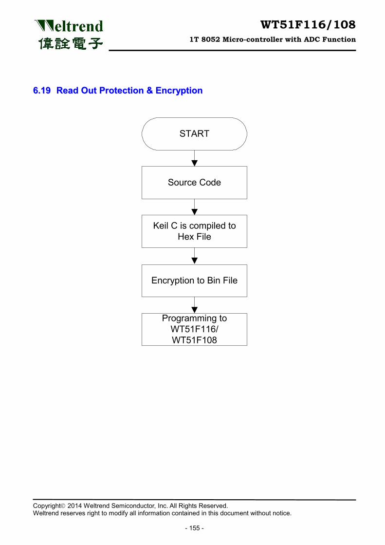
WT51F116/108 1T 8052 Micro-controller with ADC Function
Copyright 2014 Weltrend Semiconductor, Inc. All Rights Reserved. Weltrend reserves right to modify all information contained in this document without notice.
- 155 -
66..1199 RReeaadd OOuutt PPrrootteeccttiioonn && EEnnccrryyppttiioonn
Source Code
START
Keil C is compiled toHex File
Programming to WT51F116/WT51F108
Encryption to Bin File
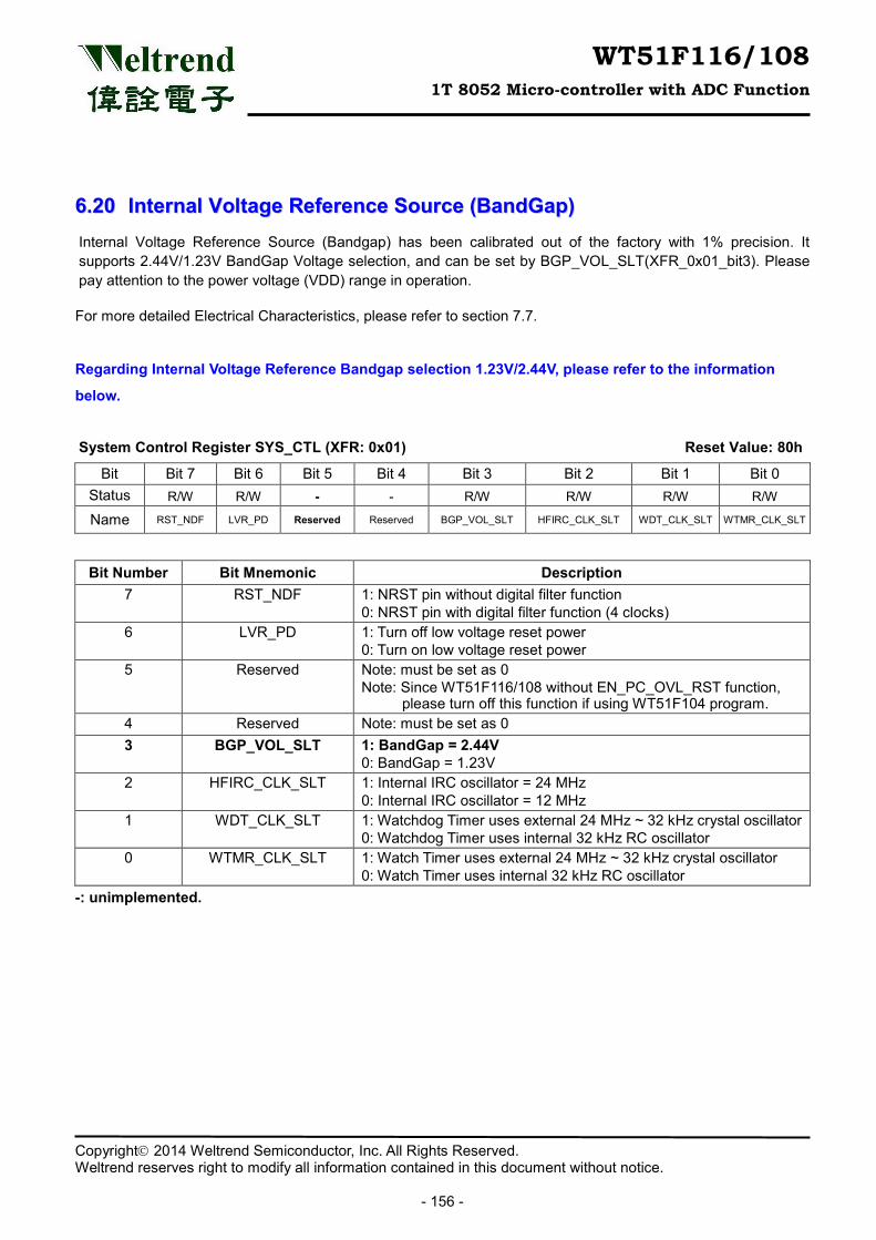
WT51F116/108 1T 8052 Micro-controller with ADC Function
Copyright 2014 Weltrend Semiconductor, Inc. All Rights Reserved. Weltrend reserves right to modify all information contained in this document without notice.
- 156 -
66..2200 IInntteerrnnaall VVoollttaaggee RReeffeerreennccee SSoouurrccee ((BBaannddGGaapp)) Internal Voltage Reference Source (Bandgap) has been calibrated out of the factory with 1% precision. It supports 2.44V/1.23V BandGap Voltage selection, and can be set by BGP_VOL_SLT(XFR_0x01_bit3). Please pay attention to the power voltage (VDD) range in operation.
For more detailed Electrical Characteristics, please refer to section 7.7.
Regarding Internal Voltage Reference Bandgap selection 1.23V/2.44V, please refer to the information
below.
System Control Register SYS_CTL (XFR: 0x01) Reset Value: 80h
Bit Bit 7 Bit 6 Bit 5 Bit 4 Bit 3 Bit 2 Bit 1 Bit 0 Status R/W R/W - - R/W R/W R/W R/W
Name RST_NDF LVR_PD Reserved Reserved BGP_VOL_SLT HFIRC_CLK_SLT WDT_CLK_SLT WTMR_CLK_SLT
Bit Number Bit Mnemonic Description 7 RST_NDF 1: NRST pin without digital filter function
0: NRST pin with digital filter function (4 clocks) 6 LVR_PD 1: Turn off low voltage reset power
0: Turn on low voltage reset power 5 Reserved Note: must be set as 0
Note: Since WT51F116/108 without EN_PC_OVL_RST function, please turn off this function if using WT51F104 program.
4 Reserved Note: must be set as 0 3 BGP_VOL_SLT 1: BandGap = 2.44V
0: BandGap = 1.23V 2 HFIRC_CLK_SLT 1: Internal IRC oscillator = 24 MHz
0: Internal IRC oscillator = 12 MHz 1 WDT_CLK_SLT 1: Watchdog Timer uses external 24 MHz ~ 32 kHz crystal oscillator
0: Watchdog Timer uses internal 32 kHz RC oscillator 0 WTMR_CLK_SLT 1: Watch Timer uses external 24 MHz ~ 32 kHz crystal oscillator
0: Watch Timer uses internal 32 kHz RC oscillator -: unimplemented.
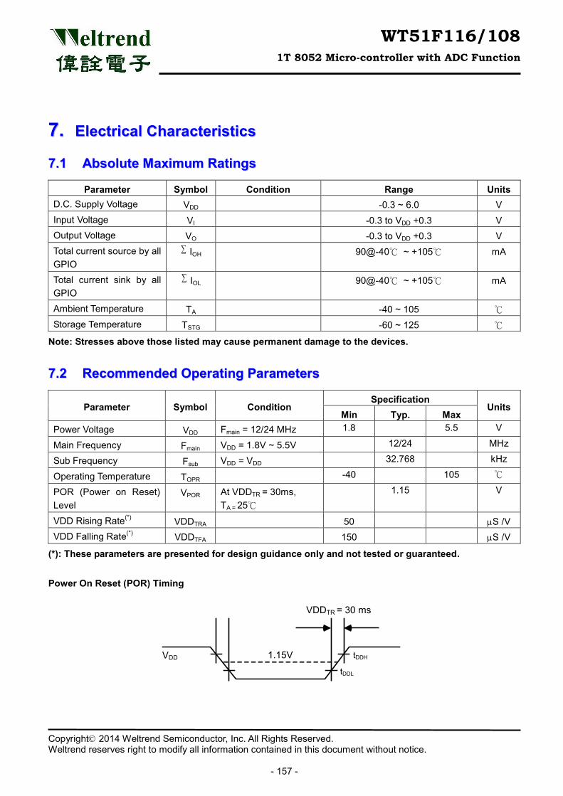
WT51F116/108 1T 8052 Micro-controller with ADC Function
Copyright 2014 Weltrend Semiconductor, Inc. All Rights Reserved. Weltrend reserves right to modify all information contained in this document without notice.
- 157 -
77..11 AAbbssoolluuttee MMaaxxiimmuumm RRaattiinnggss
Parameter Symbol Condition Range Units D.C. Supply Voltage VDD -0.3 ~ 6.0 V Input Voltage VI -0.3 to VDD +0.3 V Output Voltage VO -0.3 to VDD +0.3 V Total current source by all GPIO
∑ IOH 90@-40℃ ~ +105℃ mA
Total current sink by all GPIO
∑ IOL 90@-40℃ ~ +105℃ mA
Ambient Temperature TA -40 ~ 105 ℃ Storage Temperature TSTG -60 ~ 125 ℃
Note: Stresses above those listed may cause permanent damage to the devices.
77..22 RReeccoommmmeennddeedd OOppeerraattiinngg PPaarraammeetteerrss
Parameter Symbol Condition Specification
Units Min Typ. Max
Power Voltage VDD Fmain = 12/24 MHz 1.8 5.5 V
Main Frequency Fmain VDD = 1.8V ~ 5.5V 12/24 MHz
Sub Frequency Fsub VDD = VDD 32.768 kHz
Operating Temperature TOPR -40 105 ℃
POR (Power on Reset) Level
VPOR At VDDTR = 30ms, TA = 25℃
1.15 V
VDD Rising Rate(*) VDDTRA 50 µS /V VDD Falling Rate(*) VDDTFA 150 µS /V
(*): These parameters are presented for design guidance only and not tested or guaranteed.
Power On Reset (POR) Timing
tDDL
VDD tDDH
VDDTR = 30 ms
1.15V
77.. EElleeccttrriiccaall CChhaarraacctteerriissttiiccss
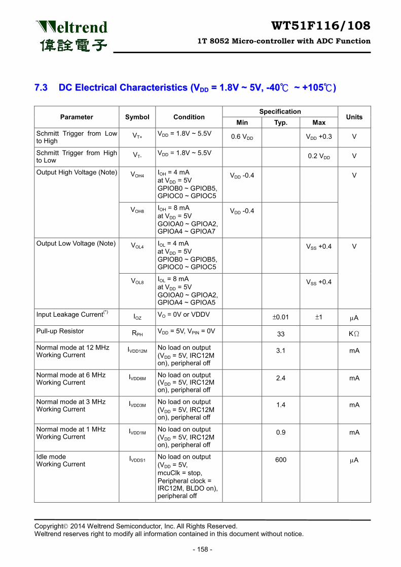
WT51F116/108 1T 8052 Micro-controller with ADC Function
Copyright 2014 Weltrend Semiconductor, Inc. All Rights Reserved. Weltrend reserves right to modify all information contained in this document without notice.
- 158 -
77..33 DDCC EElleeccttrriiccaall CChhaarraacctteerriissttiiccss ((VVDDDD == 11..88VV ~~ 55VV,, --4400℃℃ ~~ ++110055℃℃))
Parameter Symbol Condition Specification
Units Min Typ. Max
Schmitt Trigger from Low to High
VT+ VDD = 1.8V ~ 5.5V 0.6 VDD VDD +0.3 V
Schmitt Trigger from High to Low
VT- VDD = 1.8V ~ 5.5V 0.2 VDD V
Output High Voltage (Note) VOH4 IOH = 4 mA at VDD = 5V GPIOB0 ~ GPIOB5, GPIOC0 ~ GPIOC5
VDD -0.4 V
VOH8 IOH = 8 mA at VDD = 5V GOIOA0 ~ GPIOA2, GPIOA4 ~ GPIOA7
VDD -0.4
Output Low Voltage (Note) VOL4 IOL = 4 mA at VDD = 5V GPIOB0 ~ GPIOB5, GPIOC0 ~ GPIOC5
VSS +0.4 V
VOL8 IOL = 8 mA at VDD = 5V GOIOA0 ~ GPIOA2, GPIOA4 ~ GPIOA5
VSS +0.4
Input Leakage Current(*) IOZ VO = 0V or VDDV ±0.01 ±1 µA
Pull-up Resistor RPH VDD = 5V, VPIN = 0V 33 KΩ
Normal mode at 12 MHz Working Current
IVDD12M No load on output (VDD = 5V, IRC12M on), peripheral off
3.1 mA
Normal mode at 6 MHz Working Current
IVDD6M No load on output (VDD = 5V, IRC12M on), peripheral off
2.4 mA
Normal mode at 3 MHz Working Current
IVDD3M No load on output (VDD = 5V, IRC12M on), peripheral off
1.4 mA
Normal mode at 1 MHz Working Current
IVDD1M No load on output (VDD = 5V, IRC12M on), peripheral off
0.9 mA
Idle mode Working Current
IVDDS1 No load on output (VDD = 5V, mcuClk = stop, Peripheral clock = IRC12M, BLDO on), peripheral off
600 µA
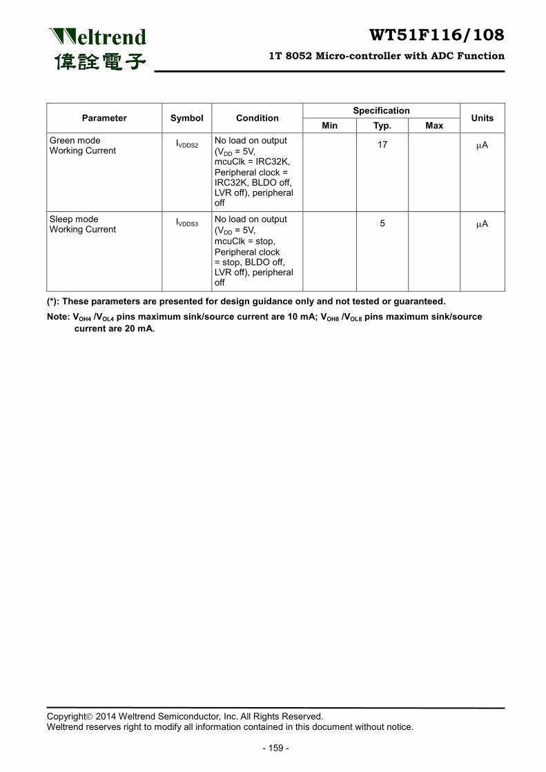
WT51F116/108 1T 8052 Micro-controller with ADC Function
Copyright 2014 Weltrend Semiconductor, Inc. All Rights Reserved. Weltrend reserves right to modify all information contained in this document without notice.
- 159 -
Parameter Symbol Condition Specification
Units Min Typ. Max
Green mode Working Current
IVDDS2 No load on output (VDD = 5V, mcuClk = IRC32K, Peripheral clock = IRC32K, BLDO off, LVR off), peripheral off
17 µA
Sleep mode Working Current
IVDDS3 No load on output (VDD = 5V, mcuClk = stop, Peripheral clock = stop, BLDO off, LVR off), peripheral off
5 µA
(*): These parameters are presented for design guidance only and not tested or guaranteed. Note: VOH4 /VOL4 pins maximum sink/source current are 10 mA; VOH8 /VOL8 pins maximum sink/source
current are 20 mA.
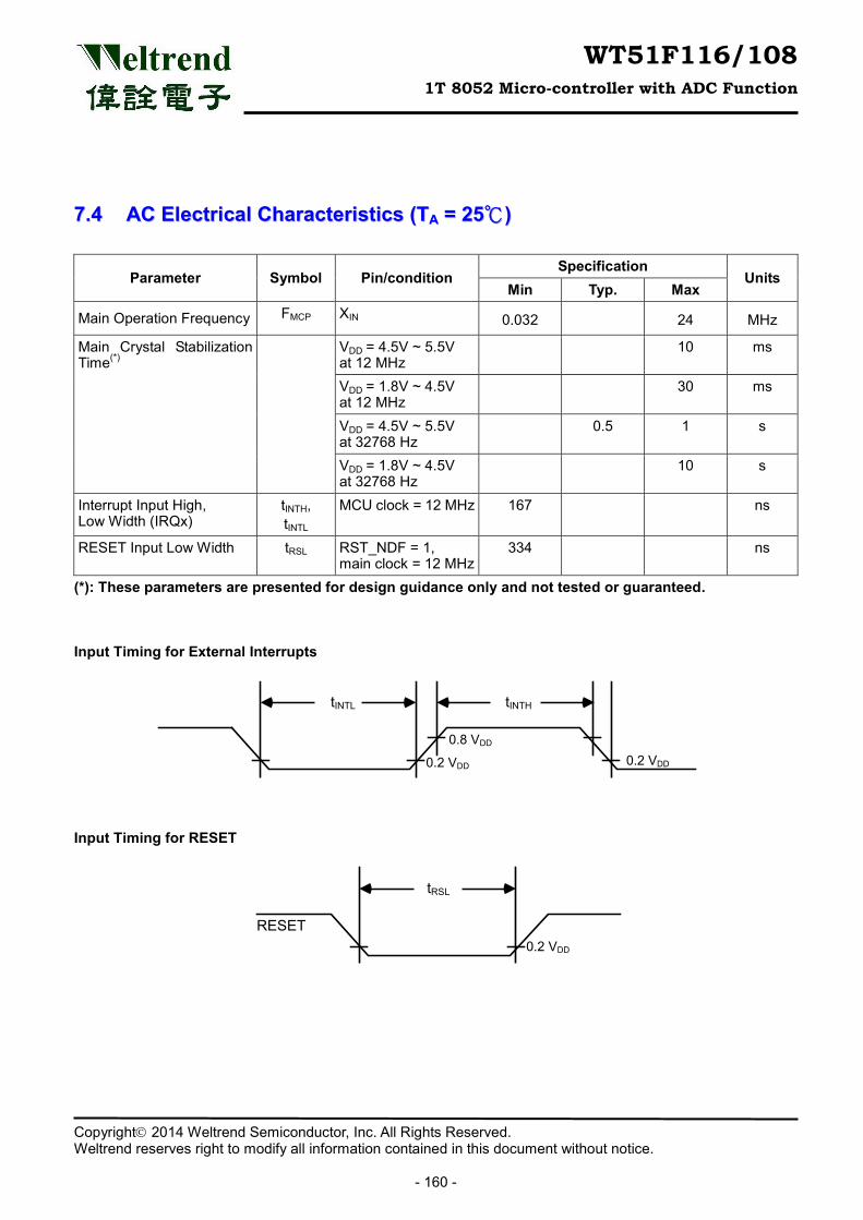
WT51F116/108 1T 8052 Micro-controller with ADC Function
Copyright 2014 Weltrend Semiconductor, Inc. All Rights Reserved. Weltrend reserves right to modify all information contained in this document without notice.
- 160 -
77..44 AACC EElleeccttrriiccaall CChhaarraacctteerriissttiiccss ((TTAA == 2255℃℃))
Parameter Symbol Pin/condition Specification
Units Min Typ. Max
Main Operation Frequency FMCP XIN 0.032 24 MHz
Main Crystal Stabilization Time(*)
VDD = 4.5V ~ 5.5V at 12 MHz
10 ms
VDD = 1.8V ~ 4.5V at 12 MHz
30 ms
VDD = 4.5V ~ 5.5V at 32768 Hz
0.5 1 s
VDD = 1.8V ~ 4.5V at 32768 Hz
10 s
Interrupt Input High, Low Width (IRQx)
tINTH, tINTL
MCU clock = 12 MHz 167 ns
RESET Input Low Width tRSL RST_NDF = 1, main clock = 12 MHz
334 ns
(*): These parameters are presented for design guidance only and not tested or guaranteed.
Input Timing for External Interrupts
tINTL
0.2 VDD
0.8 VDD
tINTH
0.2 VDD
Input Timing for RESET
tRSL
0.2 VDD
RESET
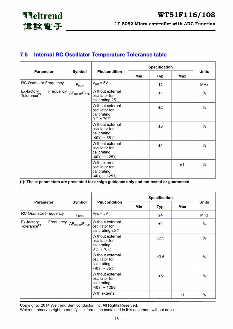
WT51F116/108 1T 8052 Micro-controller with ADC Function
Copyright 2014 Weltrend Semiconductor, Inc. All Rights Reserved. Weltrend reserves right to modify all information contained in this document without notice.
- 161 -
77..55 IInntteerrnnaall RRCC OOsscciillllaattoorr TTeemmppeerraattuurree TToolleerraannccee ttaabbllee
Parameter Symbol Pin/condition Specification
Units Min Typ. Max
RC Oscillator Frequency FRCH VDD = 5V 12 MHz
Ex-factory Frequency Tolerance(*)
ΔFRCH1/FRCH
Without external oscillator for calibrating 25℃
±1 %
Without external oscillator for calibrating 0℃ ~ 70℃
±2 %
Without external oscillator for calibrating -40℃ ~ 85℃
±3 %
Without external oscillator for calibrating -40℃ ~ 125℃
±4 %
With external oscillator for calibrating -40℃ ~ 125℃
±1 %
(*): These parameters are presented for design guidance only and not tested or guaranteed.
Parameter Symbol Pin/condition Specification
Units Min Typ. Max
RC Oscillator Frequency FRCH VDD = 5V 24 MHz
Ex-factory Frequency Tolerance(*)
ΔFRCH1/FRCH
Without external oscillator for calibrating 25℃
±1 %
Without external oscillator for calibrating 0℃ ~ 70℃
±2.5 %
Without external oscillator for calibrating -40℃ ~ 85℃
±3.5 %
Without external oscillator for calibrating -40℃ ~ 125℃
±5 %
With external ±1 %
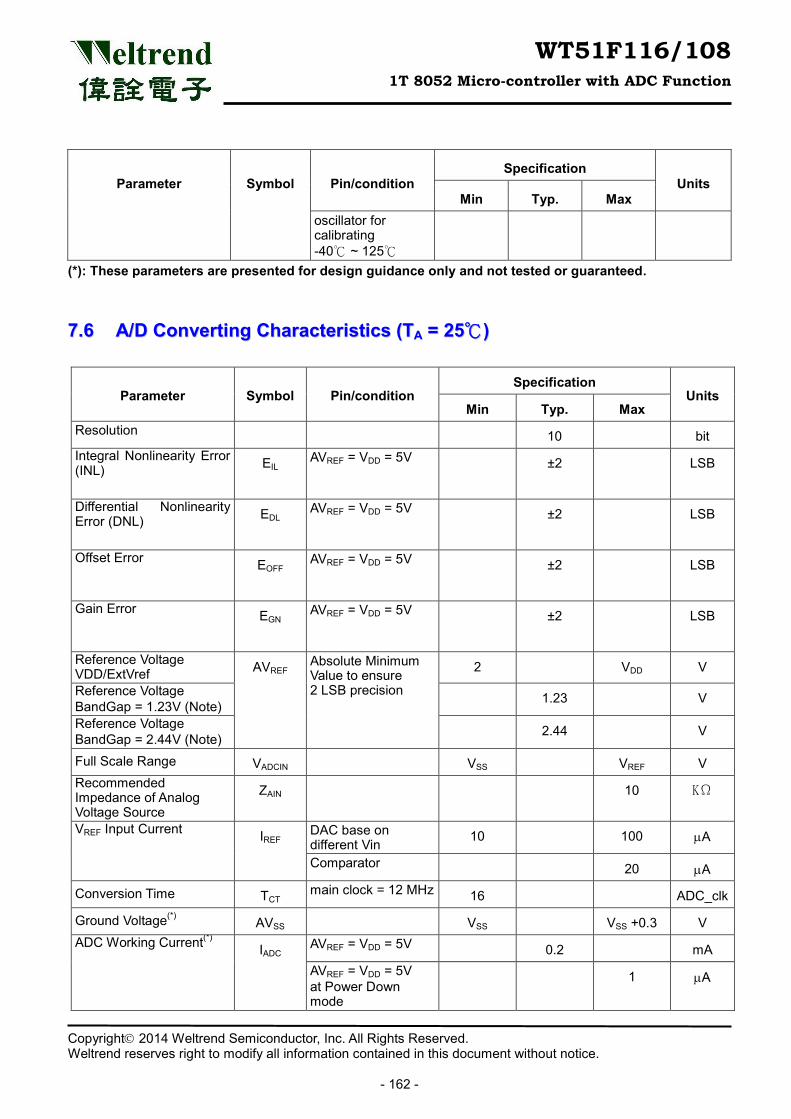
WT51F116/108 1T 8052 Micro-controller with ADC Function
Copyright 2014 Weltrend Semiconductor, Inc. All Rights Reserved. Weltrend reserves right to modify all information contained in this document without notice.
- 162 -
Parameter Symbol Pin/condition Specification
Units Min Typ. Max
oscillator for calibrating -40℃ ~ 125℃
(*): These parameters are presented for design guidance only and not tested or guaranteed.
77..66 AA//DD CCoonnvveerrttiinngg CChhaarraacctteerriissttiiccss ((TTAA == 2255℃℃))
Parameter Symbol Pin/condition Specification
Units Min Typ. Max
Resolution 10 bit Integral Nonlinearity Error (INL) EIL AVREF = VDD = 5V
±2
LSB
Differential Nonlinearity Error (DNL) EDL AVREF = VDD = 5V
±2
LSB
Offset Error EOFF AVREF = VDD = 5V
±2
LSB
Gain Error EGN AVREF = VDD = 5V
±2
LSB
Reference Voltage VDD/ExtVref AVREF Absolute Minimum
Value to ensure 2 LSB precision
2 VDD V
Reference Voltage BandGap = 1.23V (Note) 1.23 V
Reference Voltage BandGap = 2.44V (Note) 2.44 V
Full Scale Range VADCIN VSS VREF V Recommended Impedance of Analog Voltage Source
ZAIN 10 KΩ
VREF Input Current IREF DAC base on different Vin 10 100 µA
Comparator 20 µA
Conversion Time TCT main clock = 12 MHz 16 ADC_clk
Ground Voltage(*) AVSS VSS VSS +0.3 V ADC Working Current(*) IADC AVREF = VDD = 5V 0.2 mA
AVREF = VDD = 5V at Power Down mode
1 µA
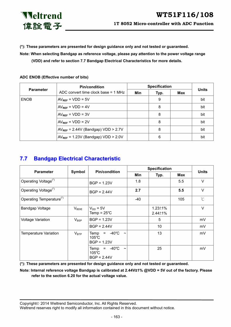
WT51F116/108 1T 8052 Micro-controller with ADC Function
Copyright 2014 Weltrend Semiconductor, Inc. All Rights Reserved. Weltrend reserves right to modify all information contained in this document without notice.
- 163 -
(*): These parameters are presented for design guidance only and not tested or guaranteed.
Note: When selecting Bandgap as reference voltage, please pay attention to the power voltage range
(VDD) and refer to section 7.7 Bandgap Electrical Characteristics for more details.
ADC ENOB (Effective number of bits)
Parameter Pin/condition
ADC convert time clock base = 1 MHz Specification
Units Min Typ. Max
ENOB AVREF = VDD = 5V 9 bit
AVREF = VDD = 4V 8 bit
AVREF = VDD = 3V 8 bit
AVREF = VDD = 2V 8 bit
AVREF = 2.44V (Bandgap) VDD > 2.7V 8 bit
AVREF = 1.23V (Bandgap) VDD > 2.0V 6 bit
77..77 BBaannddggaapp EElleeccttrriiccaall CChhaarraacctteerriissttiicc
Parameter Symbol Pin/condition Specification
Units Min Typ. Max
Operating Voltage(*) BGP = 1.23V 1.8 5.5 V
Operating Voltage(*) BGP = 2.44V 2.7 5.5 V
Operating Temperature(*) -40 105 ℃
Bandgap Voltage VBDIE VDD = 5V Temp = 25℃
1.23±1% 2.44±1%
V
Voltage Variation VBSP BGP = 1.23V 5 mV
BGP = 2.44V 10 mV
Temperature Variation VBTP Temp = -40℃ ~ 105℃ BGP = 1.23V
13 mV
Temp = -40℃ ~ 105℃ BGP = 2.44V
25 mV
(*): These parameters are presented for design guidance only and not tested or guaranteed. Note: Internal reference voltage Bandgap is calibrated at 2.44V±1% @VDD = 5V out of the factory. Please
refer to the section 6.20 for the actual voltage value.
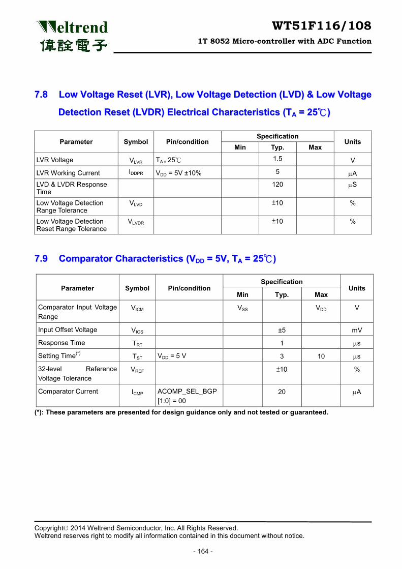
WT51F116/108 1T 8052 Micro-controller with ADC Function
Copyright 2014 Weltrend Semiconductor, Inc. All Rights Reserved. Weltrend reserves right to modify all information contained in this document without notice.
- 164 -
77..88 LLooww VVoollttaaggee RReesseett ((LLVVRR)),, LLooww VVoollttaaggee DDeetteeccttiioonn ((LLVVDD)) && LLooww VVoollttaaggee
DDeetteeccttiioonn RReesseett ((LLVVDDRR)) EElleeccttrriiccaall CChhaarraacctteerriissttiiccss ((TTAA == 2255℃℃))
Parameter Symbol Pin/condition Specification
Units Min Typ. Max
LVR Voltage VLVR TA = 25℃ 1.5 V
LVR Working Current IDDPR VDD = 5V ±10% 5 µA LVD & LVDR Response Time
120 µS
Low Voltage Detection Range Tolerance
VLVD ±10 %
Low Voltage Detection Reset Range Tolerance
VLVDR ±10 %
77..99 CCoommppaarraattoorr CChhaarraacctteerriissttiiccss ((VVDDDD == 55VV,, TTAA == 2255℃℃))
Parameter Symbol Pin/condition Specification
Units Min Typ. Max
Comparator Input Voltage Range
VICM VSS VDD V
Input Offset Voltage VIOS ±5 mV
Response Time TRT 1 µs
Setting Time(*) TST VDD = 5 V 3 10 µs
32-level Reference Voltage Tolerance
VREF ±10 %
Comparator Current ICMP ACOMP_SEL_BGP [1:0] = 00
20 µA
(*): These parameters are presented for design guidance only and not tested or guaranteed.
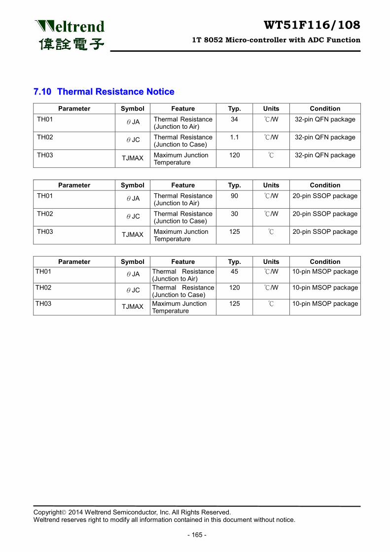
WT51F116/108 1T 8052 Micro-controller with ADC Function
Copyright 2014 Weltrend Semiconductor, Inc. All Rights Reserved. Weltrend reserves right to modify all information contained in this document without notice.
- 165 -
77..1100 TThheerrmmaall RReessiissttaannccee NNoottiiccee
Parameter Symbol Feature Typ. Units Condition TH01 θJA Thermal Resistance
(Junction to Air) 34 ℃/W 32-pin QFN package
TH02 θJC Thermal Resistance (Junction to Case)
1.1 ℃/W 32-pin QFN package
TH03 TJMAX Maximum Junction Temperature
120 ℃ 32-pin QFN package
Parameter Symbol Feature Typ. Units Condition TH01 θJA Thermal Resistance
(Junction to Air) 90 ℃/W 20-pin SSOP package
TH02 θJC Thermal Resistance (Junction to Case)
30 ℃/W 20-pin SSOP package
TH03 TJMAX Maximum Junction Temperature
125 ℃ 20-pin SSOP package
Parameter Symbol Feature Typ. Units Condition TH01 θJA Thermal Resistance
(Junction to Air) 45 ℃/W 10-pin MSOP package
TH02 θJC Thermal Resistance (Junction to Case)
120 ℃/W 10-pin MSOP package
TH03 TJMAX Maximum Junction Temperature
125 ℃ 10-pin MSOP package
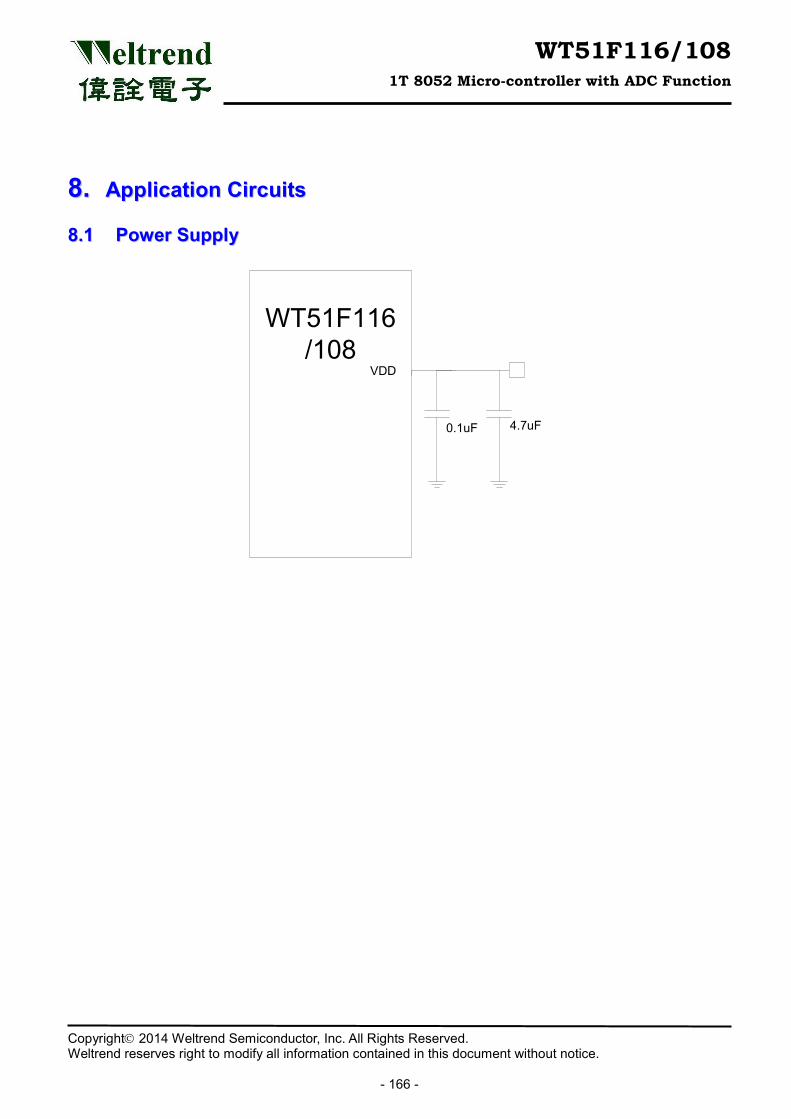
WT51F116/108 1T 8052 Micro-controller with ADC Function
Copyright 2014 Weltrend Semiconductor, Inc. All Rights Reserved. Weltrend reserves right to modify all information contained in this document without notice.
- 166 -
88..11 PPoowweerr SSuuppppllyy
WT51F116/108
VDD
0.1uF 4.7uF
88.. AApppplliiccaattiioonn CCiirrccuuiittss
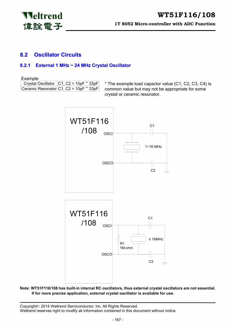
WT51F116/108 1T 8052 Micro-controller with ADC Function
Copyright 2014 Weltrend Semiconductor, Inc. All Rights Reserved. Weltrend reserves right to modify all information contained in this document without notice.
- 167 -
88..22 OOsscciillllaattoorr CCiirrccuuiittss
88..22..11 EExxtteerrnnaall 11 MMHHzz ~~ 2244 MMHHzz CCrryyssttaall OOsscciillllaattoorr
ExampleCrystal Oscillator C1, C2 = 10pF ~ 33pF
Ceramic Resonator C1, C2 = 10pF ~ 33pF* The example load capactor value (C1, C2, C3, C4) is common value but may not be appropriate for some crystal or ceramic resonator.
WT51F116/108
OSCI
OSCO
C1
C2
1~16 MHz
WT51F116/108
OSCI
OSCO
C1
C2
≥ 16MHz
1M-ohmR1
Note: WT51F116/108 has built-in internal RC oscillators, thus external crystal oscillators are not essential.
If for more precise application, external crystal oscillator is available for use.
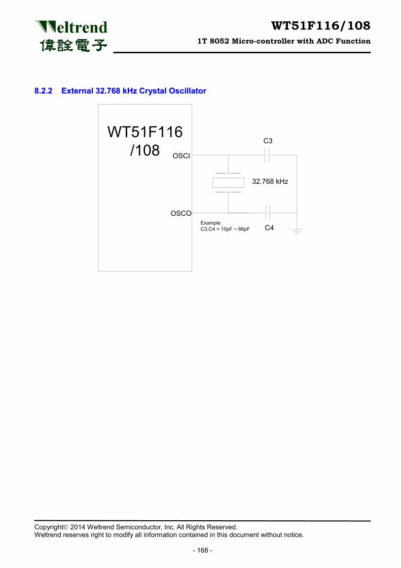
WT51F116/108 1T 8052 Micro-controller with ADC Function
Copyright 2014 Weltrend Semiconductor, Inc. All Rights Reserved. Weltrend reserves right to modify all information contained in this document without notice.
- 168 -
88..22..22 EExxtteerrnnaall 3322..776688 kkHHzz CCrryyssttaall OOsscciillllaattoorr
WT51F116/108
OSCI
OSCO
C3
C4
32.768 kHz
ExampleC3,C4 = 10pF ~ 66pF
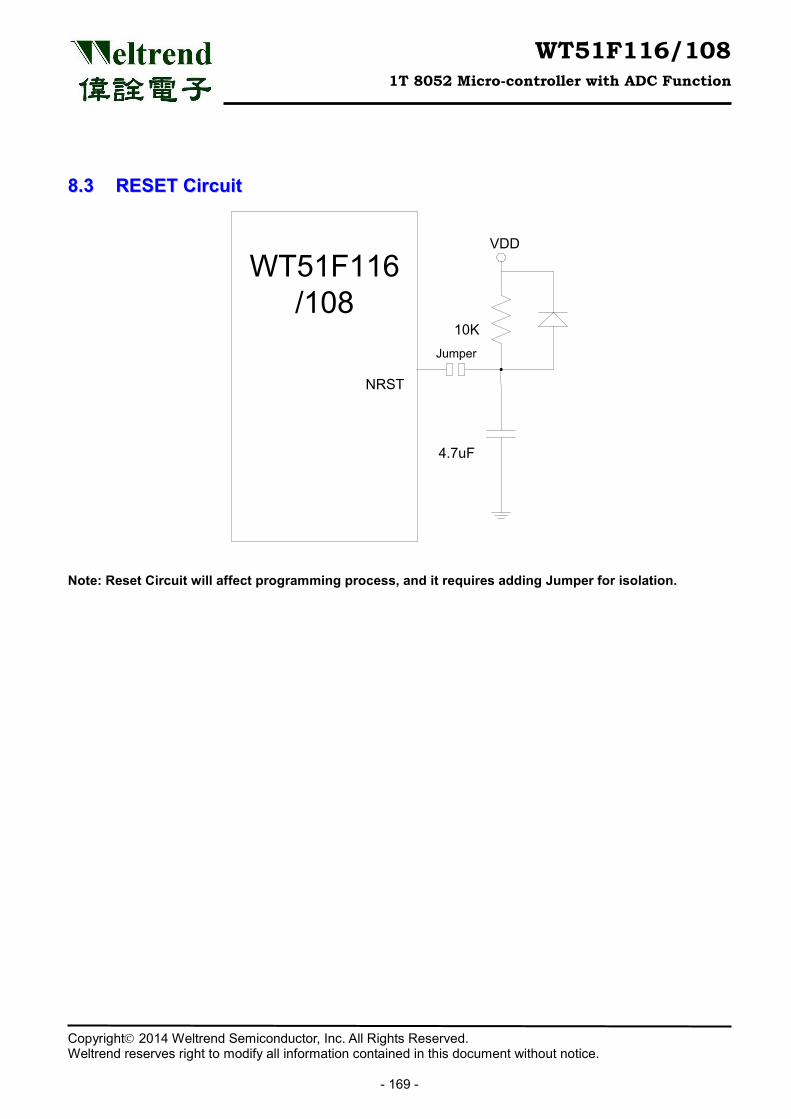
WT51F116/108 1T 8052 Micro-controller with ADC Function
Copyright 2014 Weltrend Semiconductor, Inc. All Rights Reserved. Weltrend reserves right to modify all information contained in this document without notice.
- 169 -
88..33 RREESSEETT CCiirrccuuiitt
WT51F116/108
NRST
VDD
10K
4.7uF
Jumper
Note: Reset Circuit will affect programming process, and it requires adding Jumper for isolation.
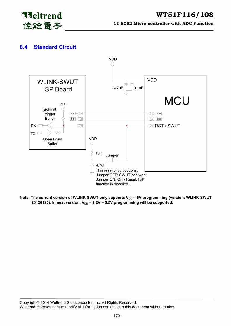
WT51F116/108 1T 8052 Micro-controller with ADC Function
Copyright 2014 Weltrend Semiconductor, Inc. All Rights Reserved. Weltrend reserves right to modify all information contained in this document without notice.
- 170 -
88..44 SSttaannddaarrdd CCiirrccuuiitt
0.1uF4.7uF
VDD
MCU
VDD
VDD
10K
4.7uF
RST / SWUT
Jumper
WLINK-SWUTISP Board
Open DrainBuffer
This reset circuit options. Jumper OFF: SWUT can workJumper ON: Only Reset, ISP function is disabled.
RX
TX
VDD
GND
VDD
GND
VDD
Schmitt triggerBuffer
Note: The current version of WLINK-SWUT only supports VDD = 5V programming (version: WLINK-SWUT 20120120). In next version, VDD = 2.2V ~ 5.5V programming will be supported.
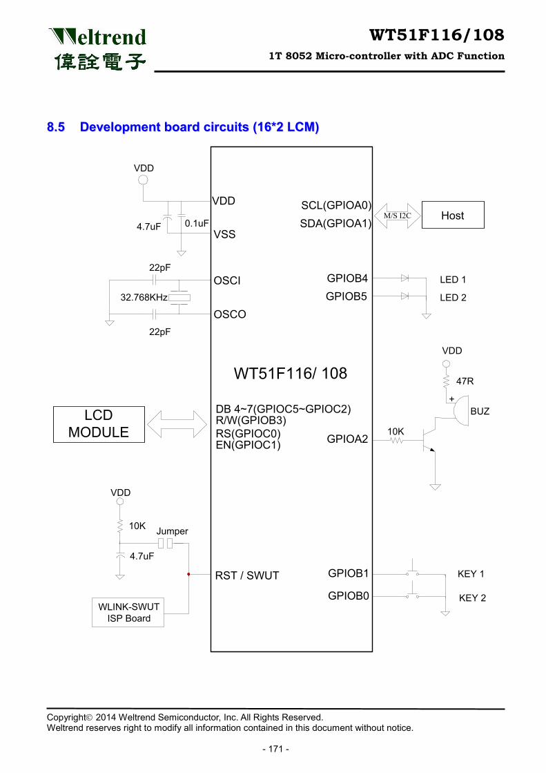
WT51F116/108 1T 8052 Micro-controller with ADC Function
Copyright 2014 Weltrend Semiconductor, Inc. All Rights Reserved. Weltrend reserves right to modify all information contained in this document without notice.
- 171 -
88..55 DDeevveellooppmmeenntt bbooaarrdd cciirrccuuiittss ((1166**22 LLCCMM))
0.1uF4.7uF
VDD
WT51F116/ 108
VDD
22pF
22pF
32.768KHz
OSCO
OSCI
RST / SWUT
GPIOB0
GPIOB1
GPIOA2
SCL(GPIOA0)SDA(GPIOA1)
M/S I2C
KEY 1
KEY 2
Host
GPIOB4GPIOB5
LED 1
LED 2
LCD MODULE
DB 4~7(GPIOC5~GPIOC2)R/W(GPIOB3)RS(GPIOC0)EN(GPIOC1)
VSS
VDD
BUZ
47R
10K
+
VDD
10K
4.7uF
Jumper
WLINK-SWUTISP Board
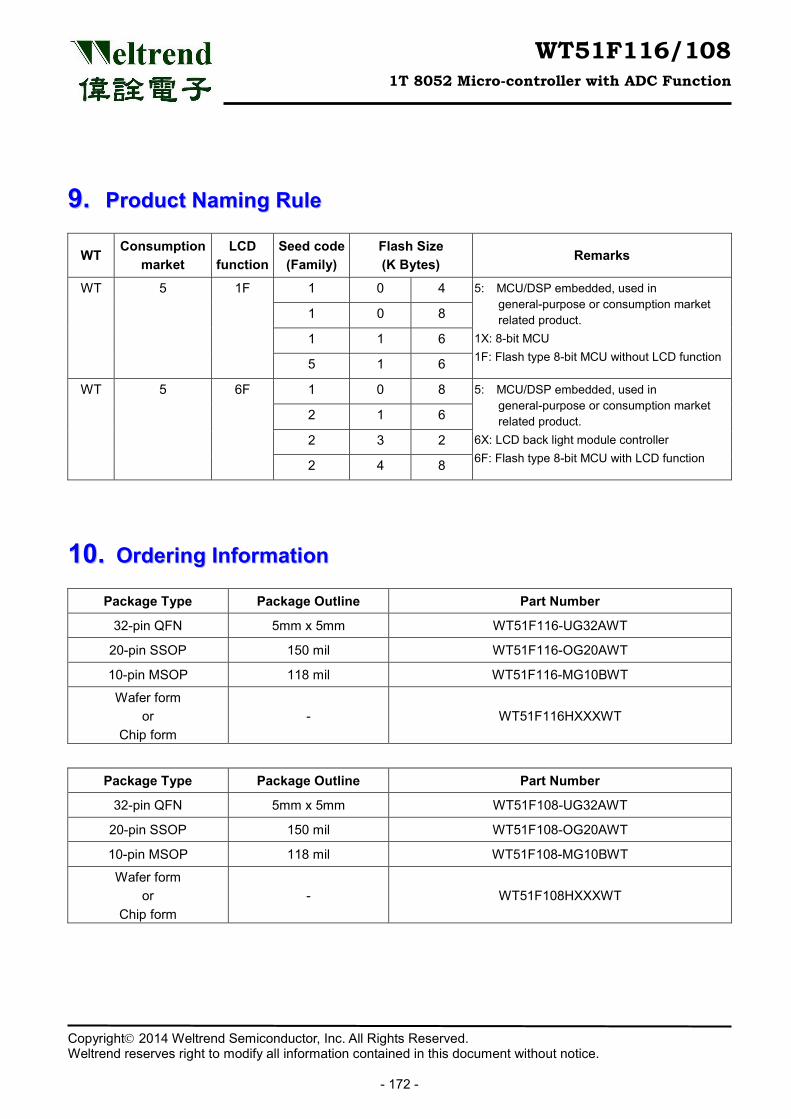
WT51F116/108 1T 8052 Micro-controller with ADC Function
Copyright 2014 Weltrend Semiconductor, Inc. All Rights Reserved. Weltrend reserves right to modify all information contained in this document without notice.
- 172 -
WT Consumption
market LCD
function Seed code
(Family) Flash Size (K Bytes)
Remarks
WT 5 1F 1 0 4 5: MCU/DSP embedded, used in general-purpose or consumption market related product.
1X: 8-bit MCU 1F: Flash type 8-bit MCU without LCD function
1 0 8
1 1 6
5 1 6
WT 5 6F 1 0 8 5: MCU/DSP embedded, used in general-purpose or consumption market related product.
6X: LCD back light module controller 6F: Flash type 8-bit MCU with LCD function
2 1 6
2 3 2
2 4 8
Package Type Package Outline Part Number
32-pin QFN 5mm x 5mm WT51F116-UG32AWT
20-pin SSOP 150 mil WT51F116-OG20AWT
10-pin MSOP 118 mil WT51F116-MG10BWT
Wafer form or
Chip form - WT51F116HXXXWT
Package Type Package Outline Part Number
32-pin QFN 5mm x 5mm WT51F108-UG32AWT
20-pin SSOP 150 mil WT51F108-OG20AWT
10-pin MSOP 118 mil WT51F108-MG10BWT
Wafer form or
Chip form - WT51F108HXXXWT
99.. PPrroodduucctt NNaammiinngg RRuullee
1100.. OOrrddeerriinngg IInnffoorrmmaattiioonn
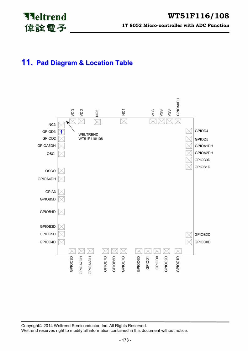
WT51F116/108 1T 8052 Micro-controller with ADC Function
Copyright 2014 Weltrend Semiconductor, Inc. All Rights Reserved. Weltrend reserves right to modify all information contained in this document without notice.
- 173 -
WELTREND WT51F116/108
VD
D
VD
D
NC
1
NC
2
VS
S
VS
S
VS
S
GPIOA5DH
OSCI
OSCO
GPIOA4DH
GPIA3
GPIOB3D
GP
IOC
3D
GP
IOA
7DH
GP
IOA
6DH
GP
IOB
7D
GP
IOB
6D
GP
IOC
7D
GP
IOD
1
GP
IOD
0
GP
IOC
2D
GP
IOC
1D
GPIOC0D
GPIOB2D
GPIOB1D
GPIOA2DH
GP
IOA
0DH
GPIOB0D
GPIOA1DH
GPIOD5
GPIOD4
GP
IOC
6D
GPIOC4D
GPIOC5D
GPIOB4D
GPIOB5D
GPIOD2
GPIOD3
NC3
1
1111.. PPaadd DDiiaaggrraamm && LLooccaattiioonn TTaabbllee
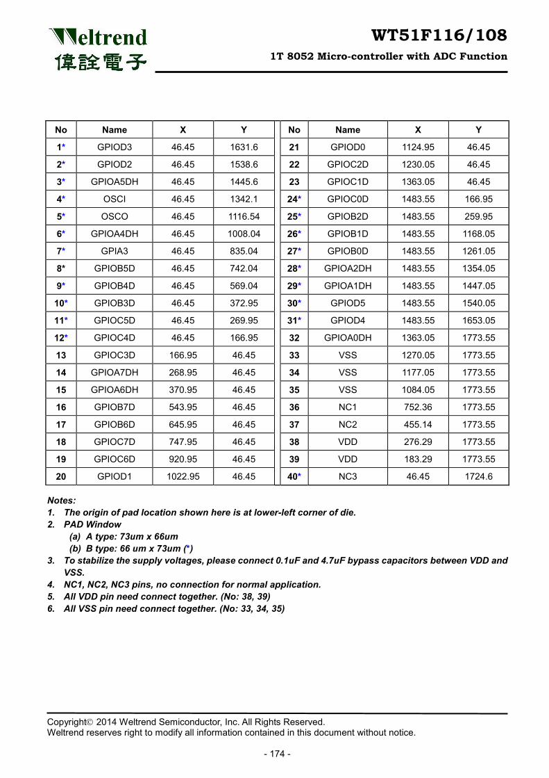
WT51F116/108 1T 8052 Micro-controller with ADC Function
Copyright 2014 Weltrend Semiconductor, Inc. All Rights Reserved. Weltrend reserves right to modify all information contained in this document without notice.
- 174 -
No Name X Y No Name X Y
1* GPIOD3 46.45 1631.6 21 GPIOD0 1124.95 46.45
2* GPIOD2 46.45 1538.6 22 GPIOC2D 1230.05 46.45
3* GPIOA5DH 46.45 1445.6 23 GPIOC1D 1363.05 46.45
4* OSCI 46.45 1342.1 24* GPIOC0D 1483.55 166.95
5* OSCO 46.45 1116.54 25* GPIOB2D 1483.55 259.95
6* GPIOA4DH 46.45 1008.04 26* GPIOB1D 1483.55 1168.05
7* GPIA3 46.45 835.04 27* GPIOB0D 1483.55 1261.05
8* GPIOB5D 46.45 742.04 28* GPIOA2DH 1483.55 1354.05
9* GPIOB4D 46.45 569.04 29* GPIOA1DH 1483.55 1447.05
10* GPIOB3D 46.45 372.95 30* GPIOD5 1483.55 1540.05
11* GPIOC5D 46.45 269.95 31* GPIOD4 1483.55 1653.05
12* GPIOC4D 46.45 166.95 32 GPIOA0DH 1363.05 1773.55
13 GPIOC3D 166.95 46.45 33 VSS 1270.05 1773.55
14 GPIOA7DH 268.95 46.45 34 VSS 1177.05 1773.55
15 GPIOA6DH 370.95 46.45 35 VSS 1084.05 1773.55
16 GPIOB7D 543.95 46.45 36 NC1 752.36 1773.55
17 GPIOB6D 645.95 46.45 37 NC2 455.14 1773.55
18 GPIOC7D 747.95 46.45 38 VDD 276.29 1773.55
19 GPIOC6D 920.95 46.45 39 VDD 183.29 1773.55
20 GPIOD1 1022.95 46.45 40* NC3 46.45 1724.6
Notes: 1. The origin of pad location shown here is at lower-left corner of die. 2. PAD Window
(a) A type: 73um x 66um (b) B type: 66 um x 73um (*)
3. To stabilize the supply voltages, please connect 0.1uF and 4.7uF bypass capacitors between VDD and VSS.
4. NC1, NC2, NC3 pins, no connection for normal application. 5. All VDD pin need connect together. (No: 38, 39) 6. All VSS pin need connect together. (No: 33, 34, 35)
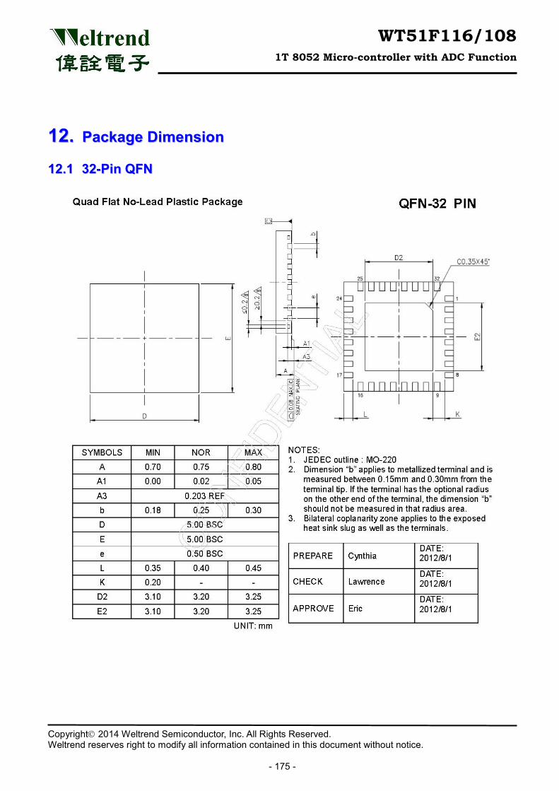
WT51F116/108 1T 8052 Micro-controller with ADC Function
Copyright 2014 Weltrend Semiconductor, Inc. All Rights Reserved. Weltrend reserves right to modify all information contained in this document without notice.
- 175 -
1122..11 3322--PPiinn QQFFNN
1122.. PPaacckkaaggee DDiimmeennssiioonn
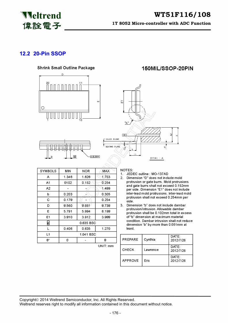
WT51F116/108 1T 8052 Micro-controller with ADC Function
Copyright 2014 Weltrend Semiconductor, Inc. All Rights Reserved. Weltrend reserves right to modify all information contained in this document without notice.
- 176 -
1122..22 2200--PPiinn SSSSOOPP
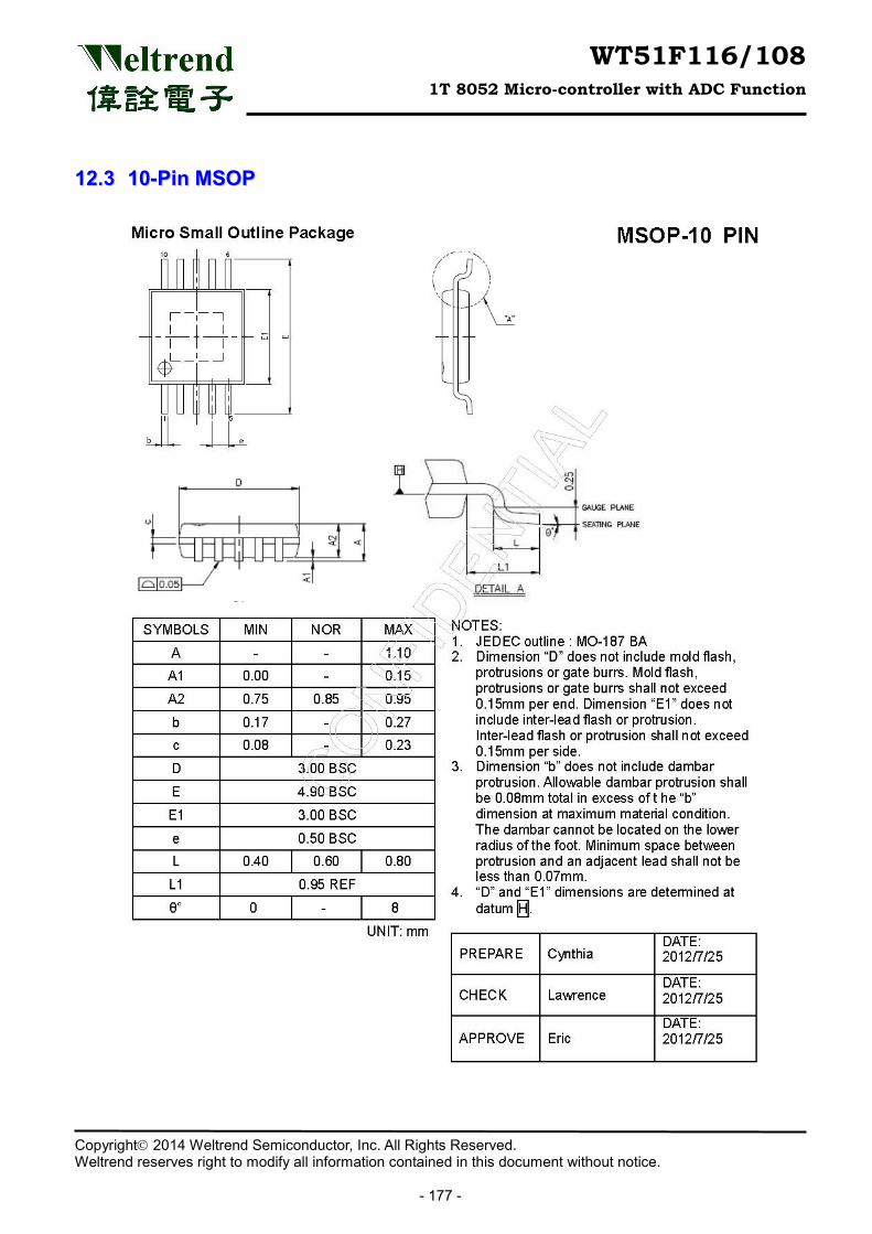
WT51F116/108 1T 8052 Micro-controller with ADC Function
Copyright 2014 Weltrend Semiconductor, Inc. All Rights Reserved. Weltrend reserves right to modify all information contained in this document without notice.
- 177 -
1122..33 1100--PPiinn MMSSOOPP
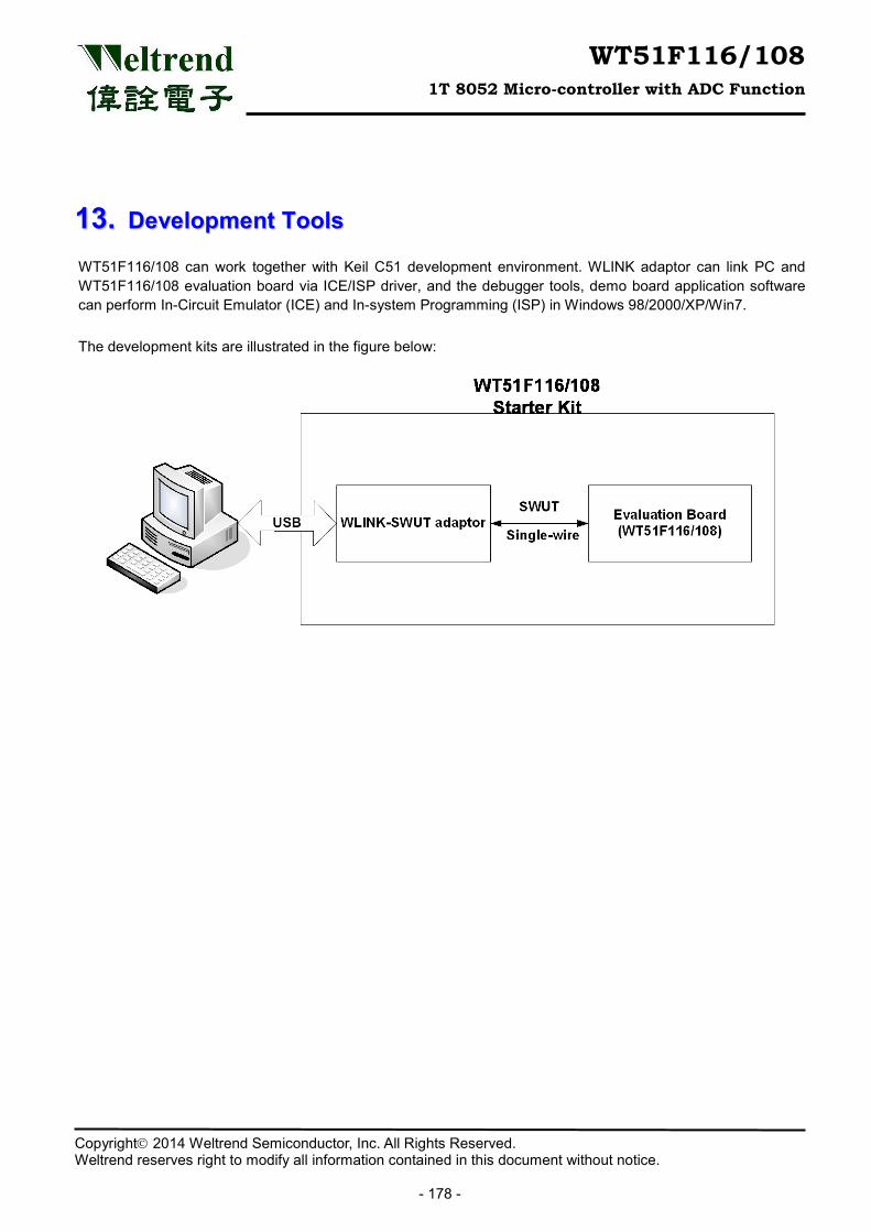
WT51F116/108 1T 8052 Micro-controller with ADC Function
Copyright 2014 Weltrend Semiconductor, Inc. All Rights Reserved. Weltrend reserves right to modify all information contained in this document without notice.
- 178 -
WT51F116/108 can work together with Keil C51 development environment. WLINK adaptor can link PC and WT51F116/108 evaluation board via ICE/ISP driver, and the debugger tools, demo board application software can perform In-Circuit Emulator (ICE) and In-system Programming (ISP) in Windows 98/2000/XP/Win7. The development kits are illustrated in the figure below:
1133.. DDeevveellooppmmeenntt TToooollss
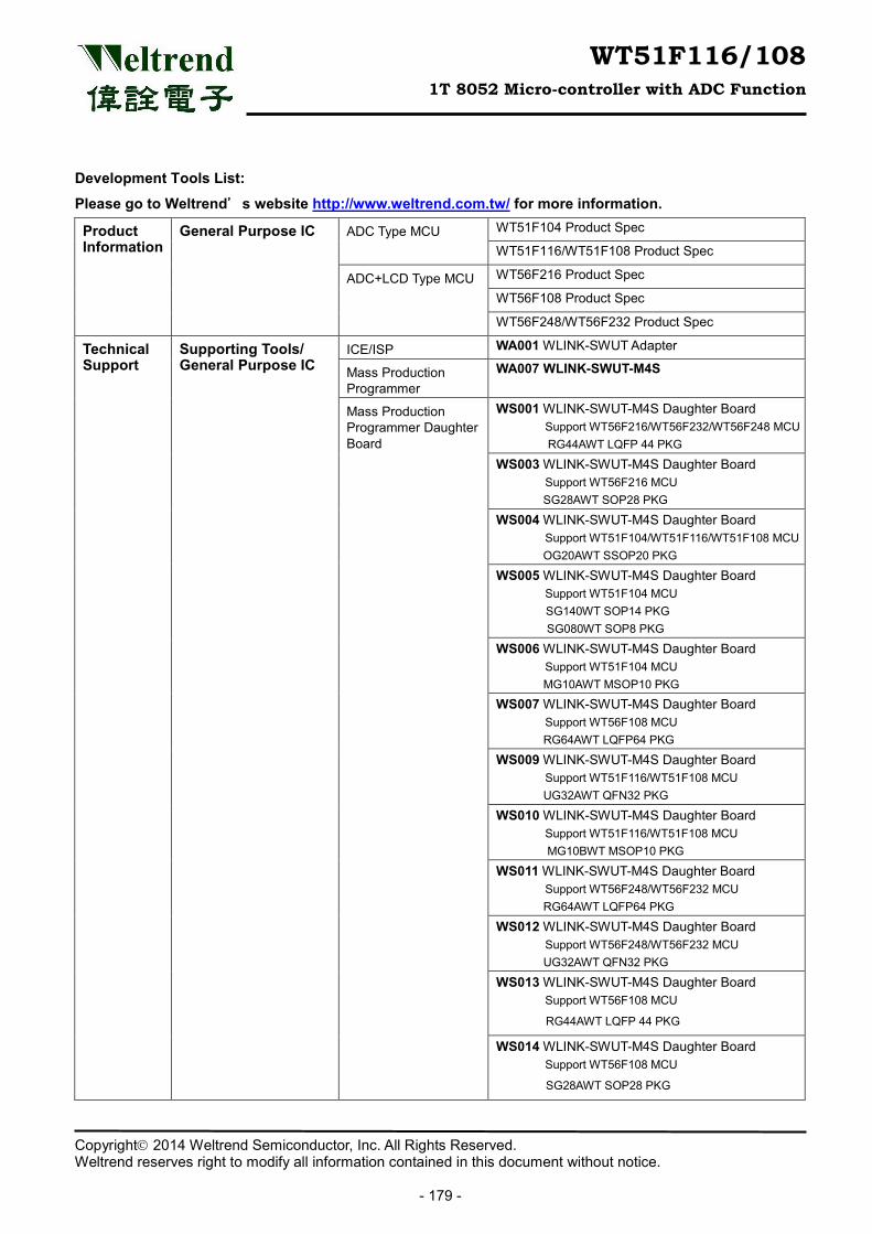
WT51F116/108 1T 8052 Micro-controller with ADC Function
Copyright 2014 Weltrend Semiconductor, Inc. All Rights Reserved. Weltrend reserves right to modify all information contained in this document without notice.
- 179 -
Development Tools List:
Please go to Weltrend’s website http://www.weltrend.com.tw/ for more information.
Product Information
General Purpose IC ADC Type MCU WT51F104 Product Spec
WT51F116/WT51F108 Product Spec
ADC+LCD Type MCU WT56F216 Product Spec
WT56F108 Product Spec
WT56F248/WT56F232 Product Spec
Technical Support
Supporting Tools/ General Purpose IC
ICE/ISP WA001 WLINK-SWUT Adapter
Mass Production Programmer
WA007 WLINK-SWUT-M4S
Mass Production Programmer Daughter Board
WS001 WLINK-SWUT-M4S Daughter Board Support WT56F216/WT56F232/WT56F248 MCU RG44AWT LQFP 44 PKG
WS003 WLINK-SWUT-M4S Daughter Board Support WT56F216 MCU
SG28AWT SOP28 PKG WS004 WLINK-SWUT-M4S Daughter Board
Support WT51F104/WT51F116/WT51F108 MCU OG20AWT SSOP20 PKG
WS005 WLINK-SWUT-M4S Daughter Board Support WT51F104 MCU SG140WT SOP14 PKG SG080WT SOP8 PKG
WS006 WLINK-SWUT-M4S Daughter Board Support WT51F104 MCU
MG10AWT MSOP10 PKG WS007 WLINK-SWUT-M4S Daughter Board
Support WT56F108 MCU RG64AWT LQFP64 PKG WS009 WLINK-SWUT-M4S Daughter Board
Support WT51F116/WT51F108 MCU UG32AWT QFN32 PKG WS010 WLINK-SWUT-M4S Daughter Board
Support WT51F116/WT51F108 MCU MG10BWT MSOP10 PKG
WS011 WLINK-SWUT-M4S Daughter Board Support WT56F248/WT56F232 MCU
RG64AWT LQFP64 PKG WS012 WLINK-SWUT-M4S Daughter Board
Support WT56F248/WT56F232 MCU UG32AWT QFN32 PKG WS013 WLINK-SWUT-M4S Daughter Board
Support WT56F108 MCU
RG44AWT LQFP 44 PKG
WS014 WLINK-SWUT-M4S Daughter Board Support WT56F108 MCU
SG28AWT SOP28 PKG
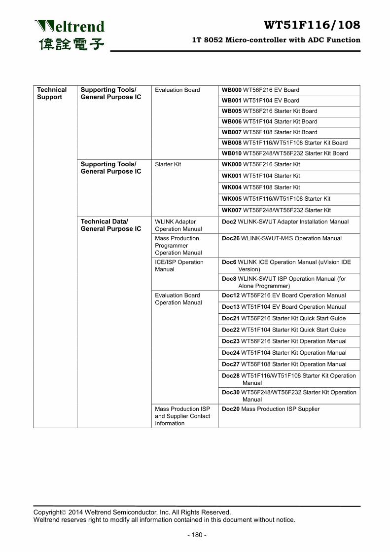
WT51F116/108 1T 8052 Micro-controller with ADC Function
Copyright 2014 Weltrend Semiconductor, Inc. All Rights Reserved. Weltrend reserves right to modify all information contained in this document without notice.
- 180 -
Technical Support
Supporting Tools/ General Purpose IC
Evaluation Board WB000 WT56F216 EV Board
WB001 WT51F104 EV Board
WB005 WT56F216 Starter Kit Board
WB006 WT51F104 Starter Kit Board
WB007 WT56F108 Starter Kit Board
WB008 WT51F116/WT51F108 Starter Kit Board
WB010 WT56F248/WT56F232 Starter Kit Board
Supporting Tools/ General Purpose IC
Starter Kit WK000 WT56F216 Starter Kit
WK001 WT51F104 Starter Kit
WK004 WT56F108 Starter Kit
WK005 WT51F116/WT51F108 Starter Kit
WK007 WT56F248/WT56F232 Starter Kit
Technical Data/ General Purpose IC
WLINK Adapter Operation Manual
Doc2 WLINK-SWUT Adapter Installation Manual
Mass Production Programmer Operation Manual
Doc26 WLINK-SWUT-M4S Operation Manual
ICE/ISP Operation Manual
Doc6 WLINK ICE Operation Manual (uVision IDE Version)
Doc8 WLINK-SWUT ISP Operation Manual (for Alone Programmer)
Evaluation Board Operation Manual
Doc12 WT56F216 EV Board Operation Manual
Doc13 WT51F104 EV Board Operation Manual
Doc21 WT56F216 Starter Kit Quick Start Guide
Doc22 WT51F104 Starter Kit Quick Start Guide
Doc23 WT56F216 Starter Kit Operation Manual
Doc24 WT51F104 Starter Kit Operation Manual
Doc27 WT56F108 Starter Kit Operation Manual
Doc28 WT51F116/WT51F108 Starter Kit Operation Manual
Doc30 WT56F248/WT56F232 Starter Kit Operation Manual
Mass Production ISP and Supplier Contact Information
Doc20 Mass Production ISP Supplier
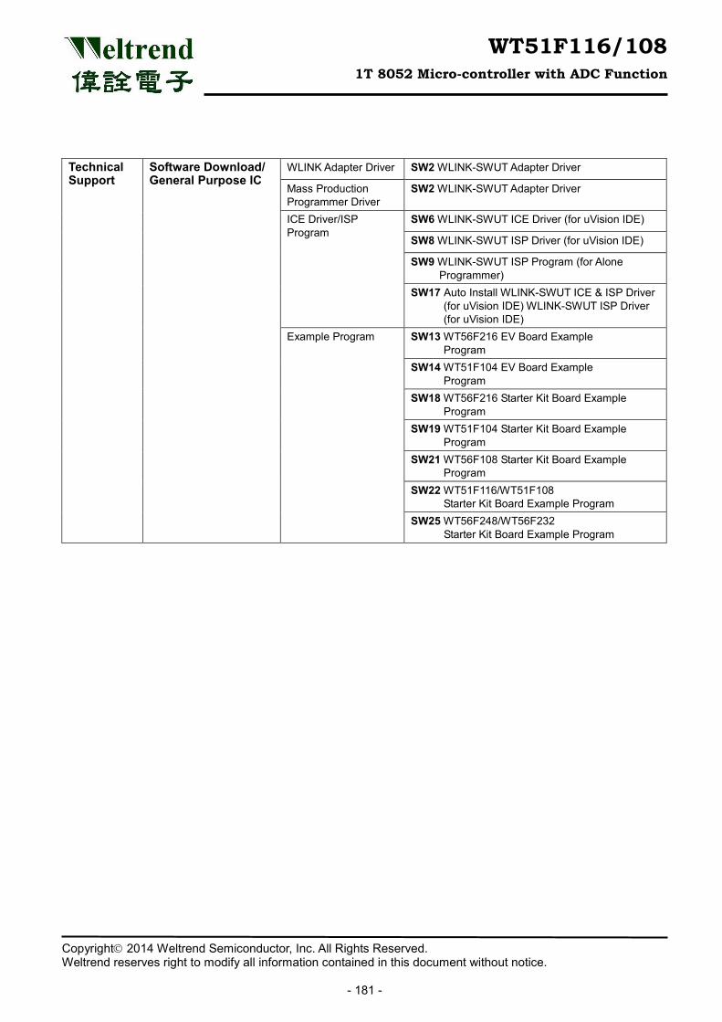
WT51F116/108 1T 8052 Micro-controller with ADC Function
Copyright 2014 Weltrend Semiconductor, Inc. All Rights Reserved. Weltrend reserves right to modify all information contained in this document without notice.
- 181 -
Technical Support
Software Download/ General Purpose IC
WLINK Adapter Driver SW2 WLINK-SWUT Adapter Driver
Mass Production Programmer Driver
SW2 WLINK-SWUT Adapter Driver
ICE Driver/ISP Program
SW6 WLINK-SWUT ICE Driver (for uVision IDE)
SW8 WLINK-SWUT ISP Driver (for uVision IDE)
SW9 WLINK-SWUT ISP Program (for Alone Programmer)
SW17 Auto Install WLINK-SWUT ICE & ISP Driver (for uVision IDE) WLINK-SWUT ISP Driver (for uVision IDE)
Example Program SW13 WT56F216 EV Board Example Program
SW14 WT51F104 EV Board Example Program
SW18 WT56F216 Starter Kit Board Example Program
SW19 WT51F104 Starter Kit Board Example Program
SW21 WT56F108 Starter Kit Board Example Program
SW22 WT51F116/WT51F108 Starter Kit Board Example Program
SW25 WT56F248/WT56F232 Starter Kit Board Example Program
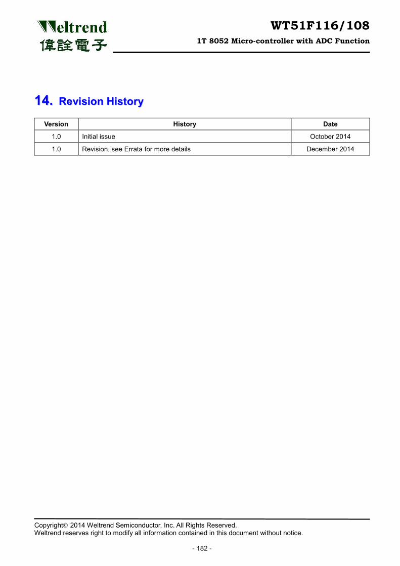
WT51F116/108 1T 8052 Micro-controller with ADC Function
Copyright 2014 Weltrend Semiconductor, Inc. All Rights Reserved. Weltrend reserves right to modify all information contained in this document without notice.
- 182 -
Version History Date
1.0 Initial issue October 2014
1.0 Revision, see Errata for more details December 2014
1144.. RReevviissiioonn HHiissttoorryy
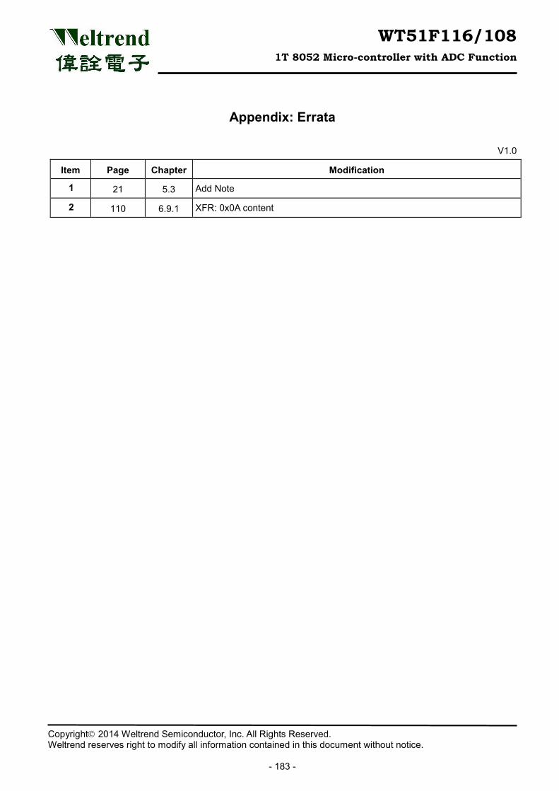
WT51F116/108 1T 8052 Micro-controller with ADC Function
Copyright 2014 Weltrend Semiconductor, Inc. All Rights Reserved. Weltrend reserves right to modify all information contained in this document without notice.
- 183 -
Appendix: Errata
V1.0
Item Page Chapter Modification
1 21 5.3 Add Note
2 110 6.9.1 XFR: 0x0A content