Working with PLLs in PrimeTime - Zimmer Design … · 2013-03-11 · Working with PLLs in PrimeTime...
135
Working with PLLs in PrimeTime – avoiding the “phase locked oops” Paul Zimmer Zimmer Design Services 1375 Sun Tree Drive Roseville, CA 95661 [email protected] website: www.zimmerdesignservices.com ABSTRACT . PLLs play an important role in modern high-speed designs, especially when configured for clock tree insertion delay cancellation (IDC). Modeling the behavior of such PLLs accurately in PrimeTime can be a challenge. This paper discusses basic modeling techniques for both standard and multiplier IDC PLLs, duty cycle modeling, jitter and skew, and on-chip-variation effects. The classic OCV/PLL excess pessimism problem will be explained and examined, and a couple of workarounds will be discussed, including a novel new technique developed by the author.
Transcript of Working with PLLs in PrimeTime - Zimmer Design … · 2013-03-11 · Working with PLLs in PrimeTime...

Working with PLLs in PrimeTime
– avoiding the “phase locked oops”
Paul Zimmer
Zimmer Design Services
1375 Sun Tree Drive
Roseville, CA 95661
website: www.zimmerdesignservices.com
ABSTRACT
.
PLLs play an important role in modern high-speed designs, especially when configured for clock
tree insertion delay cancellation (IDC). Modeling the behavior of such PLLs accurately in
PrimeTime can be a challenge. This paper discusses basic modeling techniques for both standard
and multiplier IDC PLLs, duty cycle modeling, jitter and skew, and on-chip-variation effects.
The classic OCV/PLL excess pessimism problem will be explained and examined, and a couple
of workarounds will be discussed, including a novel new technique developed by the author.

SNUG San Jose 2005 Working with PLLs in PrimeTime 2
Table of contents
1 Introduction ............................................................................................................................. 3
2 The basic insertion delay cancellation (idc) PLL .................................................................... 4 2.1 The problem – too much delay ............................................................................................................................ 4 2.2 The solution – the insertion delay cancellation PLL ............................................................................................ 5 2.3 Timing the basic idc PLL in PrimeTime .............................................................................................................. 6 2.4 The IDC multiplier PLL .................................................................................................................................... 15 2.5 The PLL model itself ..................................................................................................................................... 2324 2.6 Performance considerations ........................................................................................................................... 2425
3 Duty Cycle ........................................................................................................................ 2526 3.1 Internal clocks (other than PLLs)................................................................................................................... 2526 3.2 Primary input clocks and PLLs ...................................................................................................................... 2728 3.3 Applying this to our multiplier pll circuit .................................................................................................. 343533 3.4 When to use these techniques .................................................................................................................... 404139
4 Jitter .............................................................................................................................. 414240 4.1 Jitter, skew, and uncertainty ....................................................................................................................... 414240 4.2 My definition of jitter ................................................................................................................................ 414240 4.3 Sources of jitter .......................................................................................................................................... 424341 4.4 Effects of jitter on different sorts of paths ................................................................................................. 424341 4.5 Modeling jitter with set_clock_uncertainty ................................................................................................ 464745 4.6 Applying jitter specs to the example circuit – simple case ........................................................................ 464745 4.7 Generated clocks ........................................................................................................................................ 535452 4.8 What about falling edges? .......................................................................................................................... 555654 4.9 Applying jitter specs to the example circuit – complex case ..................................................................... 565755
5 On-chip Variation ......................................................................................................... 636462 5.1 The classic OCV case ................................................................................................................................ 636462 5.2 Enter CRPR ............................................................................................................................................... 666765 5.3 OCV and PLLs .......................................................................................................................................... 686967 5.4 The OCV/PLL excess pessimism problem ................................................................................................ 747573
6 OCV/PLL excess pessimism workarounds ................................................................... 787977 6.1 Forcing OCV off on the fb path ................................................................................................................. 787977 6.2 Referencing the i/os to the feedback clock ................................................................................................ 959694 6.3 The shell game ..................................................................................................................................... 103105103
7 Conclusion .............................................................................................................. 110111109
8 Acknowledgements ................................................................................................. 111112110
9 References ............................................................................................................... 112113111
10 Appendix ............................................................................................................. 113114112 10.1 The PLL model itself ......................................................................................................................... 113114112 10.2 Why I do it my way............................................................................................................................ 128130128 10.3 Modeling duty cycle using set_clock_latency early/late .................................................................... 129130128 10.4 Modeling duty cycle using set_clock_latency min/max ..................................................................... 133135133

SNUG San Jose 2005 Working with PLLs in PrimeTime 3
1 Introduction
PLLs are an absolutely essential tool in high-speed design. Their ability to nearly zero out the
delay of a large clock tree allows for much higher speed inter-chip communication.
However, modeling PLLs in static timing analysis is tricky. Many of the details have been
glossed over or ignored in the past, but as circuit feature sizes decrease and speeds increase, it is
no longer acceptable to depend on over-constrained budgets or just plain dumb luck to be sure
the PLL will work in the intended application. Certain effects, such as on-chip variation and
signal integrity analysis, make correct operation of the circuit absolutely dependent on a
complete, accurate static timing analysis – and this includes the PLL.

SNUG San Jose 2005 Working with PLLs in PrimeTime 4
2 The basic insertion delay cancellation (idc) PLL
PLLs are common in modern high-speed designs. The inner workings of the pll are more the
domain of analog sorcerers, but the basic idea is this: “the pll makes its output do whatever is
necessary to make its ref and fb inputs match in phase and frequency”.
There are many uses for PLLs. The one I’ll be discussing here is what I call the “insertion delay
cancellation” pll.
2.1 The problem – too much delay
Here is a very basic i/o circuit. Data and clock are sent in and data comes out. The outgoing data
is clocked externally by the same clock that is sent to the circuit.
Figure 2-1
And here’s what the timing waveform looks like:
Figure 2-2
It is clear that all of the delays in generating the data (clock pad, clock tree insertion delay, etc)
Tsu

SNUG San Jose 2005 Working with PLLs in PrimeTime 5
will reduce the available setup time of dout and therefore limit the frequency of operation.
2.2 The solution – the insertion delay cancellation PLL
To get around this problem, designers often insert a PLL into the clock path. The configuration
looks like this:
Figure 2-3
The Fb input of the pll is connected to the end of the clock tree.
Remember that the pll must drive its output such that its ref and fb inputs match in phase and
frequency. The frequency part is easy – it just matches clkin’s frequency, which reappears on the
Fb pin. What about the phase?
Ignore Tref for now. If the clock at Ref arrived at time zero, the pll would have to drive its
output back in time by Tfb to make the signal arrive at the Fb pin at time zero. So, it would
launch the clock at time –Tfb. But, clkin appears at the pll Ref pin at time Tref. So, the pll
doesn’t have to drive its output back by the full Tfb, but only by Tfb – Tref. In other words, it
launches its clock at time Tref – Tfb. After passing through the feedback loop, the clock arrives
at the Fb input at time Tref, which is what we want.
Ref
Fb
Out
Tref
Tfb

SNUG San Jose 2005 Working with PLLs in PrimeTime 6
The net effect of this is that the flops on the end of the clock tree get clocked at almost time zero.
They get clocked at time Tref. If we add a little extra delay to the feedback path to match Tref,
we can get the flops clocked at time zero relative to clkin. This allows us to “cancel” the
insertion delay of the clock tree. So, a more realistic idc pll might look like this:
Figure 2-4
2.3 Timing the basic idc PLL in PrimeTime
So, how do we go about modeling this in Primetime? The most straightforward approach
(although not the only approach, as we shall see later) is to model what happens in real life –
create a clock on the pll output pin with a frequency to match clkin, and then “launch” this pll
output clock at time Tref-Tfb. We then allow the two clocks to time against one another. The
“launch” is accomplished with the set_clock_latency command, so the commands would look
something like this:
create_clock -period 10.0 -name clkin [get_ports clkin]
set_propagated_clock clkin
create_clock -period 10.0 -name pllout [get_pins PLL/OUT]
set_propagated_clock pllout
set_clock_latency -source \
[expr $_ref_delay - $_fb_delay] \
[get_clocks pllout]
The problem is, how do we get the values of $_ref_delay and $_fb_delay?
Reference [4] gives one approach. I use a different approach. I use get_timing_paths to get the
values. I think mine is simpler to code. It also takes advantage of the fact that, by creating all the
clocks first, it is possible to extract the feedback delay as an arrival attribute on the fb pin. Also,
reference [4] puts the values into files that are then sourced by multiple Primetime runs. I’m not
that trusting, so I force PT to calculate the value every time the script runs.

SNUG San Jose 2005 Working with PLLs in PrimeTime 7
My approach is like this:
1. Create all the clocks, including the pll output clock (but don’t set the source latency yet).
2. Get Tref and Tfb using get_timing_paths.
3. Calculate the source latency (Tref – Tfb) and apply it to the pll output clock. The source
latency value will usually be negative.
4. Use set_input_delay and set_output_delay with the reference clock to specify the i/o timing.
5. Allow the clocks to time against each other (don’t do set_false_path between them)
Here’s an example circuit. I have added a flip-flop on the end of the clock tree. The flop clocks
data in through the din pad, and sends data out through the dout pad. Notice also that this flop is
on a slightly different branch of the clock tree than the one the pll feedback is hooked up to.
They share clktree_root, but not clktree1 (to the flop) or clktree2 (to the pll feedback).
Figure 2-5
First, we’ll create the clocks. Doing this first makes it easier to get the delay values we want:
create_clock -period 10.0 -name clkin [get_ports clkin]
set_propagated_clock clkin
create_clock -period 10.0 -name pllout [get_pins PLL/OUT]
set_propagated_clock pllout
Tfb
Tref
SNUG San Jose 2005 Working with PLLs in PrimeTime 8
Because the clocks exists, we can get the timing values we want by just getting the “arrival”
attribute on the path:
set _path [get_timing_paths -delay max_rise \
-from [get_ports clkin] \
-to [get_pins PLL/CKREF] \
]
set _ref_delay [get_attribute $_path arrival]
set _path [get_timing_paths -delay max_rise \
-from [get_pins PLL/OUT] \
-to [get_pins PLL/FB] \
]
set _fb_delay [get_attribute $_path arrival]
Note the use of “-delay max_rise”. We want a rise delay because the pll runs on rising edges
(most do, anyway). Without on-chip-variation (OCV), the min_rise and max_rise values should
be the same. OCV effects will be discussed later.
Also note that _ref_delay is set by getting the arrival attribute on the path returned by
get_timing_paths, which is a collection. I expect this collection to have only one path in it. If I
have done something wrong and the collection has more than one path, the “set _ref_delay”
command will cause an error. I call this poor-man’s error checking…
When I run this script, I get:
pt_shell> echo $_ref_delay
1.000000
pt_shell> echo $_fb_delay
3.300000
pt_shell>

SNUG San Jose 2005 Working with PLLs in PrimeTime 9
Let’s verify this using report_timing. We’ll need to set the variable
timing_report_unconstrained_paths to “true” to see a result.
pt_shell> set timing_report_unconstrained_paths true
true
pt_shell> report_timing -input_pins -delay max_rise -from [get_ports clkin] -
to [get_pins PLL/CKREF]
****************************************
Report : timing
-path full
-delay max_rise
-input_pins
-max_paths 1
Design : idc_pll_example
Version: V-2004.06
****************************************
Startpoint: clkin (clock source 'clkin')
Endpoint: PLL/CKREF (internal pin)
Path Group: (none)
Path Type: max
Point Incr Path
---------------------------------------------------------------
clock source latency 0.00 0.00
clkin (in) 0.00 0.00 r
clkinpad/I (bufbd1) 0.00 0.00 r
clkinpad/Z (bufbd1) 1.00 * 1.00 r
PLL/CKREF (DUMMYPLL) 0.00 1.00 r
data arrival time 1.00
---------------------------------------------------------------
(Path is unconstrained)

SNUG San Jose 2005 Working with PLLs in PrimeTime 10
pt_shell> report_timing -input_pins -delay max_rise -from [get_pins PLL/OUT] -
to [get_pins PLL/FB]
****************************************
Report : timing
-path full
-delay max_rise
-input_pins
-max_paths 1
Design : idc_pll_example
Version: V-2004.06
****************************************
Startpoint: PLL/OUT (clock source 'pllout')
Endpoint: PLL/FB (internal pin)
Path Group: (none)
Path Type: max
Point Incr Path
---------------------------------------------------------------
clock source latency 0.00 0.00
PLL/OUT (DUMMYPLL) 0.00 0.00 r
clktree_root/I (bufbd1) 0.00 0.00 r
clktree_root/Z (bufbd1) 2.20 * 2.20 r
clktree_2/I (bufbd1) 0.00 2.20 r
clktree_2/Z (bufbd1) 0.10 * 2.30 r
fbdelay/I (bufbd1) 0.00 2.30 r
fbdelay/Z (bufbd1) 1.00 * 3.30 r
PLL/FB (DUMMYPLL) 0.00 3.30 r
data arrival time 3.30
---------------------------------------------------------------
(Path is unconstrained)
Looks correct. $_ref_delay is 1.0 and $_fb_delay is 3.3.
Now we’ll apply this source latency:
set_clock_latency -source \
[expr $_ref_delay - $_fb_delay] \
[get_clocks pllout]
When we do this, we’ll get the following warning:
Warning: Negative clock latency specified: -2.3 (UITE-150)
This is harmless. We normally expect a negative source delay on the pll output clock (because
the fb path is usually longer than the refclk path).
SNUG San Jose 2005 Working with PLLs in PrimeTime 11
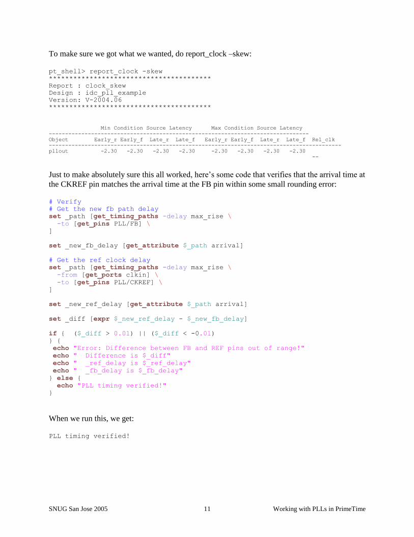
To make sure we got what we wanted, do report_clock –skew:
pt_shell> report_clock -skew
****************************************
Report : clock_skew
Design : idc_pll_example
Version: V-2004.06
****************************************
Min Condition Source Latency Max Condition Source Latency
--------------------------------------------------------------------------------
Object Early_r Early_f Late_r Late_f Early_r Early_f Late_r Late_f Rel_clk
------------------------------------------------------------------------------------------
pllout -2.30 -2.30 -2.30 -2.30 -2.30 -2.30 -2.30 -2.30
--
Just to make absolutely sure this all worked, here’s some code that verifies that the arrival time at
the CKREF pin matches the arrival time at the FB pin within some small rounding error:
# Verify
# Get the new fb path delay
set _path [get_timing_paths -delay max_rise \
-to [get_pins PLL/FB] \
]
set _new_fb_delay [get_attribute $_path arrival]
# Get the ref clock delay
set _path [get_timing_paths -delay max_rise \
-from [get_ports clkin] \
-to [get_pins PLL/CKREF] \
]
set _new_ref_delay [get_attribute $_path arrival]
set _diff [expr $_new_ref_delay - $_new_fb_delay]
if { ($_diff > 0.01) || ($_diff < -0.01)
} {
echo "Error: Difference between FB and REF pins out of range!"
echo " Difference is $_diff"
echo " _ref_delay is $_ref_delay"
echo " _fb_delay is $_fb_delay"
} else {
echo "PLL timing verified!"
}
When we run this, we get:
PLL timing verified!

SNUG San Jose 2005 Working with PLLs in PrimeTime 12
Now we need to constrain the data paths. The din/dout paths are part of an interface that is
referenced to clkin, so we’ll set the input and output delays accordingly.
set_input_delay -max 8.0 -clock clkin [get_ports din]
set_input_delay -min 0.5 -clock clkin [get_ports din]
set_output_delay -max 2.0 -clock clkin [get_ports dout]
set_output_delay -min [expr -1.0 * 0.5] -clock clkin [get_ports dout]
Now let’s look at the timing. Here’s the schematic again, with the delays of each buffer shown:
Figure 2-6
A couple of things to notice about this. I have made the fbdelay match the clkinpad delay
exactly, but the clktree_1 and clktree_2 buffers don’t match exactly. The clock tree has 0.2ns of
real skew.
1.0
1.0 0.1
0.3 2.2
2.5
1.2

SNUG San Jose 2005 Working with PLLs in PrimeTime 13
First we’ll look at the din timing:
pt_shell> report_timing -input_pins -path_type full_clock_expanded -from din
****************************************
Report : timing
-path full_clock_expanded
-delay max
-input_pins
-max_paths 1
Design : idc_pll_example
Version: V-2004.06
****************************************
Startpoint: din (input port clocked by clkin)
Endpoint: dout_reg (rising edge-triggered flip-flop clocked by pllout)
Path Group: pllout
Path Type: max
Point Incr Path
---------------------------------------------------------------
clock clkin (rise edge) 0.00 0.00
clock network delay (propagated) 0.00 0.00
input external delay 8.00 8.00 r
din (in) 0.00 8.00 r
dinpad/I (bufbd1) 0.00 8.00 r
dinpad/Z (bufbd1) 1.20 * 9.20 r
dout_reg/D (dfnrb1) 0.00 9.20 r
data arrival time 9.20
clock pllout (rise edge) 10.00 10.00
clock source latency -2.30 7.70
PLL/OUT (DUMMYPLL) 0.00 7.70 r
clktree_root/I (bufbd1) 0.00 7.70 r
clktree_root/Z (bufbd1) 2.20 * 9.90 r
clktree_1/I (bufbd1) 0.00 9.90 r
clktree_1/Z (bufbd1) 0.30 * 10.20 r
dout_reg/CP (dfnrb1) 0.00 10.20 r
library setup time -0.08 10.12
data required time 10.12
---------------------------------------------------------------
data required time 10.12
data arrival time -9.20
---------------------------------------------------------------
slack (MET) 0.92
If the insertion delay cancellation were perfect, we would expect the clock to arrive at
dout_reg/CP at time 10.0 (one full period of the clock). Instead, it arrives at 10.2. Why?
Because the clock tree had skew. The clktree_2 buffer was 0.2ns faster than the clktree_1 buffer.
This means the feeback delay from the pll was slightly less than it should have been, resulting in
a late arriving clock.
SNUG San Jose 2005 Working with PLLs in PrimeTime 14
Now let’s look at the dout timing:
pt_shell> report_timing -input_pins -path_type full_clock_expanded -to dout
****************************************
Report : timing
-path full_clock_expanded
-delay max
-input_pins
-max_paths 1
Design : idc_pll_example
Version: V-2004.06
****************************************
Startpoint: dout_reg (rising edge-triggered flip-flop clocked by pllout)
Endpoint: dout (output port clocked by clkin)
Path Group: clkin
Path Type: max
Point Incr Path
---------------------------------------------------------------
clock pllout (rise edge) 0.00 0.00
clock source latency -2.30 -2.30
PLL/OUT (DUMMYPLL) 0.00 -2.30 r
clktree_root/I (bufbd1) 0.00 -2.30 r
clktree_root/Z (bufbd1) 2.20 * -0.10 r
clktree_1/I (bufbd1) 0.00 -0.10 r
clktree_1/Z (bufbd1) 0.30 * 0.20 r
dout_reg/CP (dfnrb1) 0.00 0.20 r
dout_reg/Q (dfnrb1) 0.32 0.52 f
doutpad/I (bufbd1) 0.00 0.52 f
doutpad/Z (bufbd1) 2.50 * 3.02 f
dout (out) 0.00 3.02 f
data arrival time 3.02
clock clkin (rise edge) 10.00 10.00
clock network delay (propagated) 0.00 10.00
output external delay -2.00 8.00
data required time 8.00
---------------------------------------------------------------
data required time 8.00
data arrival time -3.02
---------------------------------------------------------------
slack (MET) 4.98
In this case, we’re launching data from the pll domain and capturing it in the clkin domain.
So, the capture clock is at 10.0. But the launch clock at dout_reg/CP is 0.20 – once again it is
0.2ns late (for the same reason explained above).
Both of these path reports are correct – we have modeled the pll behavior correctly.
SNUG San Jose 2005 Working with PLLs in PrimeTime 15
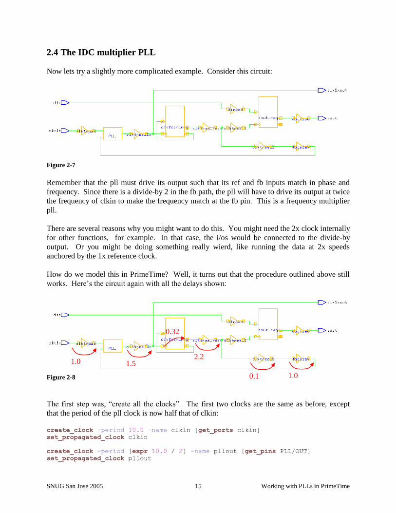
2.4 The IDC multiplier PLL
Now lets try a slightly more complicated example. Consider this circuit:
Figure 2-7
Remember that the pll must drive its output such that its ref and fb inputs match in phase and
frequency. Since there is a divide-by 2 in the fb path, the pll will have to drive its output at twice
the frequency of clkin to make the frequency match at the fb pin. This is a frequency multiplier
pll.
There are several reasons why you might want to do this. You might need the 2x clock internally
for other functions, for example. In that case, the i/os would be connected to the divide-by
output. Or you might be doing something really wierd, like running the data at 2x speeds
anchored by the 1x reference clock.
How do we model this in PrimeTime? Well, it turns out that the procedure outlined above still
works. Here’s the circuit again with all the delays shown:
Figure 2-8
The first step was, “create all the clocks”. The first two clocks are the same as before, except
that the period of the pll clock is now half that of clkin:
create_clock -period 10.0 -name clkin [get_ports clkin]
set_propagated_clock clkin
create_clock -period [expr 10.0 / 2] -name pllout [get_pins PLL/OUT]
set_propagated_clock pllout
1.0 1.5 2.2
0.1 1.0
0.32
SNUG San Jose 2005 Working with PLLs in PrimeTime 16
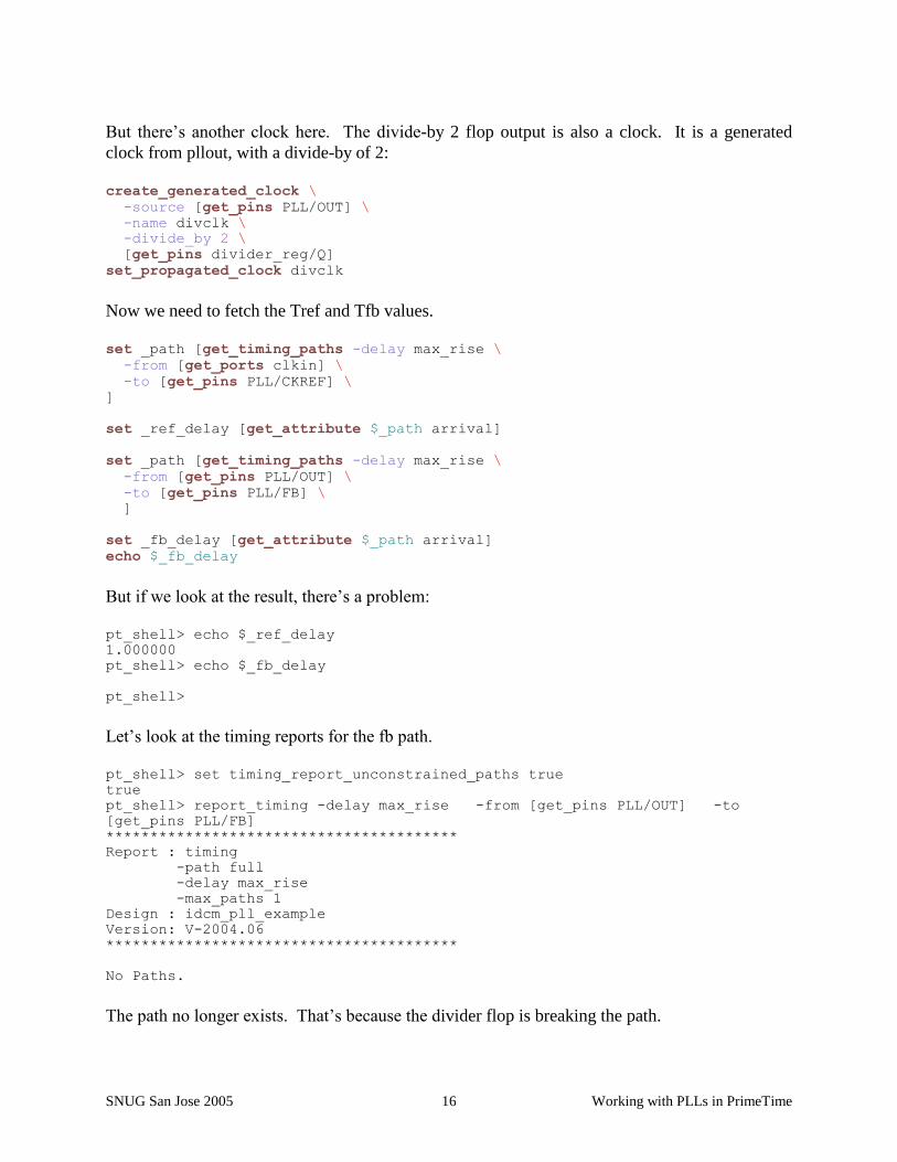
But there’s another clock here. The divide-by 2 flop output is also a clock. It is a generated
clock from pllout, with a divide-by of 2:
create_generated_clock \
-source [get_pins PLL/OUT] \
-name divclk \
-divide_by 2 \
[get_pins divider_reg/Q]
set_propagated_clock divclk
Now we need to fetch the Tref and Tfb values.
set _path [get_timing_paths -delay max_rise \
-from [get_ports clkin] \
-to [get_pins PLL/CKREF] \
]
set _ref_delay [get_attribute $_path arrival]
set _path [get_timing_paths -delay max_rise \
-from [get_pins PLL/OUT] \
-to [get_pins PLL/FB] \
]
set _fb_delay [get_attribute $_path arrival]
echo $_fb_delay
But if we look at the result, there’s a problem:
pt_shell> echo $_ref_delay
1.000000
pt_shell> echo $_fb_delay
pt_shell>
Let’s look at the timing reports for the fb path.
pt_shell> set timing_report_unconstrained_paths true
true
pt_shell> report_timing -delay max_rise -from [get_pins PLL/OUT] -to
[get_pins PLL/FB]
****************************************
Report : timing
-path full
-delay max_rise
-max_paths 1
Design : idcm_pll_example
Version: V-2004.06
****************************************
No Paths.
The path no longer exists. That’s because the divider flop is breaking the path.

SNUG San Jose 2005 Working with PLLs in PrimeTime 17
Try again with just the pll FB pin endpoint:
pt_shell> report_timing -delay max_rise -to [get_pins PLL/FB]
****************************************
Report : timing
-path full
-delay max_rise
-max_paths 1
Design : idcm_pll_example
Version: V-2004.06
****************************************
Startpoint: divider_reg/Q
(clock source 'divclk')
Endpoint: PLL/FB (internal pin)
Path Group: (none)
Path Type: max
Point Incr Path
---------------------------------------------------------------
clock source latency 1.82 1.82
divider_reg/Q (dfnrb1) 0.00 1.82 r
clktree_root/Z (bufbd1) 2.20 H 4.02 r
clktree_2/Z (bufbd1) 0.10 H 4.12 r
fbdelay/Z (bufbd1) 1.00 H 5.12 r
PLL/FB (DUMMYPLL) 0.00 5.12 r
data arrival time 5.12
---------------------------------------------------------------
(Path is unconstrained)
But is this correct? Let’s see where the “clock source latency” comes from:
pt_shell> report_timing -delay max_rise -from [get_pins divider_reg/CP] -
to [get_pins divider_reg/Q]
****************************************
Report : timing
-path full
-delay max_rise
-max_paths 1
Design : idcm_pll_example
Version: V-2004.06
****************************************
Startpoint: divider_reg
(rising edge-triggered flip-flop clocked by pllout)
Endpoint: divider_reg/Q
(internal pin)
Path Group: (none)
Path Type: max
Point Incr Path
---------------------------------------------------------------
clock network delay (propagated) 1.50 1.50
divider_reg/CP (dfnrb1) 0.00 1.50 r
divider_reg/Q (dfnrb1) 0.32 1.82 r
data arrival time 1.82
---------------------------------------------------------------
(Path is unconstrained)
SNUG San Jose 2005 Working with PLLs in PrimeTime 18
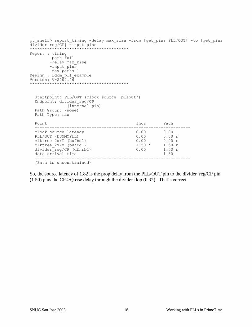
pt_shell> report_timing -delay max_rise -from [get_pins PLL/OUT] -to [get_pins
divider_reg/CP] -input_pins
****************************************
Report : timing
-path full
-delay max_rise
-input_pins
-max_paths 1
Design : idcm_pll_example
Version: V-2004.06
****************************************
Startpoint: PLL/OUT (clock source 'pllout')
Endpoint: divider_reg/CP
(internal pin)
Path Group: (none)
Path Type: max
Point Incr Path
---------------------------------------------------------------
clock source latency 0.00 0.00
PLL/OUT (DUMMYPLL) 0.00 0.00 r
clktree_2x/I (bufbd1) 0.00 0.00 r
clktree_2x/Z (bufbd1) 1.50 * 1.50 r
divider_reg/CP (dfnrb1) 0.00 1.50 r
data arrival time 1.50
---------------------------------------------------------------
(Path is unconstrained)
So, the source latency of 1.82 is the prop delay from the PLL/OUT pin to the divider_reg/CP pin
(1.50) plus the CP->Q rise delay through the divider flop (0.32). That’s correct.

SNUG San Jose 2005 Working with PLLs in PrimeTime 19
We can see this more clearly if we use –path_type full_clock_expanded with just the endpoint:
pt_shell> report_timing -delay max_rise -to [get_pins PLL/FB] -path_type
full_clock_expanded
****************************************
Report : timing
-path full_clock_expanded
-delay max_rise
-max_paths 1
Design : idcm_pll_example
Version: V-2004.06-SP1
****************************************
Startpoint: divider_reg/Q
(clock source 'divclk')
Endpoint: PLL/FB (internal pin)
Path Group: (none)
Path Type: max
Point Incr Path
---------------------------------------------------------------
clock pllout (source latency) -4.12 -4.12
PLL/OUT (DUMMYPLL) 0.00 -4.12 r
clktree_2x/Z (bufbd1) 1.50 * -2.62 r
divider_reg/Q (dfnrb1) (gclock source)
0.32 H -2.30 r
divider_reg/Q (dfnrb1) 0.00 -2.30 r
clktree_root/Z (bufbd1) 2.20 H -0.10 r
clktree_2/Z (bufbd1) 0.10 H 0.00 r
fbdelay/Z (bufbd1) 1.00 H 1.00 r
PLL/FB (DUMMYPLL) 0.00 1.00 r
data arrival time 1.00
---------------------------------------------------------------
(Path is unconstrained)
So, let’s try the _fb_delay code without the –from switch:
set _path [get_timing_paths -delay max_rise \
-to [get_pins PLL/FB] \
]
set _fb_delay [get_attribute $_path arrival]
And the value is now correct:
pt_shell> echo $_fb_delay
5.120000
pt_shell>
SNUG San Jose 2005 Working with PLLs in PrimeTime 20
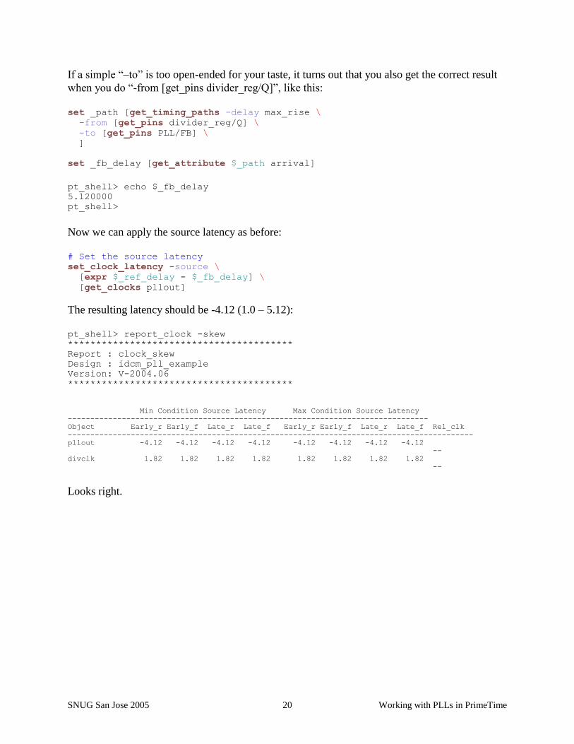
If a simple “–to” is too open-ended for your taste, it turns out that you also get the correct result
when you do “-from [get_pins divider_reg/Q]”, like this:
set _path [get_timing_paths -delay max_rise \
-from [get_pins divider_reg/Q] \
-to [get_pins PLL/FB] \
]
set _fb_delay [get_attribute $_path arrival]
pt_shell> echo $_fb_delay
5.120000
pt_shell>
Now we can apply the source latency as before:
# Set the source latency
set_clock_latency -source \
[expr $_ref_delay - $_fb_delay] \
[get_clocks pllout]
The resulting latency should be -4.12 (1.0 – 5.12):
pt_shell> report_clock -skew
****************************************
Report : clock_skew
Design : idcm_pll_example
Version: V-2004.06
****************************************
Min Condition Source Latency Max Condition Source Latency
--------------------------------------------------------------------------------
Object Early_r Early_f Late_r Late_f Early_r Early_f Late_r Late_f Rel_clk
------------------------------------------------------------------------------------------
pllout -4.12 -4.12 -4.12 -4.12 -4.12 -4.12 -4.12 -4.12
--
divclk 1.82 1.82 1.82 1.82 1.82 1.82 1.82 1.82
--
Looks right.

SNUG San Jose 2005 Working with PLLs in PrimeTime 21
The verify code will similarly have to change (remove the –from from the fb path or replace with
the –from the divider_reg):
# Verify
# Get the new fb path delay
set _path [get_timing_paths -delay max_rise \
-to [get_pins PLL/FB] \
]
set _new_fb_delay [get_attribute $_path arrival]
# Get the ref clock delay
set _path [get_timing_paths -delay max_rise \
-from [get_ports clkin] \
-to [get_pins PLL/CKREF] \
]
set _new_ref_delay [get_attribute $_path arrival]
set _diff [expr $_new_ref_delay - $_new_fb_delay]
if { ($_diff > 0.01) || ($_diff < -0.01)
} {
echo "Error: Difference between FB and REF pins out of range!"
echo " Difference is $_diff"
echo " _new_ref_delay is $_new_ref_delay"
echo " _new_fb_delay is $_new_fb_delay"
} else {
echo "PLL timing verified!"
}
And the verify works:
PLL timing verified!
Apply the i/o constraints as before:
set_input_delay -max 8.0 -clock clkin [get_ports din]
set_input_delay -min 0.5 -clock clkin [get_ports din]
set_output_delay -max 2.0 -clock clkin [get_ports dout]
set_output_delay -min [expr -1.0 * 0.5] -clock clkin [get_ports dout]
Now let’s look at some i/o timing:
pt_shell> report_timing -input_pins -path_type full_clock_expanded -from din
****************************************
Report : timing
-path full_clock_expanded
-delay max
-input_pins
-max_paths 1
Design : idcm_pll_example
Version: V-2004.06
****************************************
SNUG San Jose 2005 Working with PLLs in PrimeTime 22
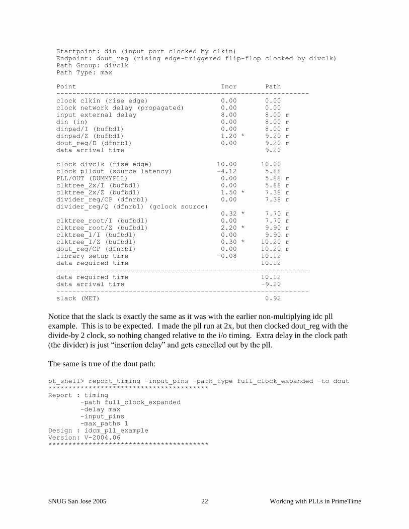
Startpoint: din (input port clocked by clkin)
Endpoint: dout_reg (rising edge-triggered flip-flop clocked by divclk)
Path Group: divclk
Path Type: max
Point Incr Path
---------------------------------------------------------------
clock clkin (rise edge) 0.00 0.00
clock network delay (propagated) 0.00 0.00
input external delay 8.00 8.00 r
din (in) 0.00 8.00 r
dinpad/I (bufbd1) 0.00 8.00 r
dinpad/Z (bufbd1) 1.20 * 9.20 r
dout_reg/D (dfnrb1) 0.00 9.20 r
data arrival time 9.20
clock divclk (rise edge) 10.00 10.00
clock pllout (source latency) -4.12 5.88
PLL/OUT (DUMMYPLL) 0.00 5.88 r
clktree_2x/I (bufbd1) 0.00 5.88 r
clktree_2x/Z (bufbd1) 1.50 * 7.38 r
divider_reg/CP (dfnrb1) 0.00 7.38 r
divider_reg/Q (dfnrb1) (gclock source)
0.32 * 7.70 r
clktree_root/I (bufbd1) 0.00 7.70 r
clktree_root/Z (bufbd1) 2.20 * 9.90 r
clktree_1/I (bufbd1) 0.00 9.90 r
clktree_1/Z (bufbd1) 0.30 * 10.20 r
dout_reg/CP (dfnrb1) 0.00 10.20 r
library setup time -0.08 10.12
data required time 10.12
---------------------------------------------------------------
data required time 10.12
data arrival time -9.20
---------------------------------------------------------------
slack (MET) 0.92
Notice that the slack is exactly the same as it was with the earlier non-multiplying idc pll
example. This is to be expected. I made the pll run at 2x, but then clocked dout_reg with the
divide-by 2 clock, so nothing changed relative to the i/o timing. Extra delay in the clock path
(the divider) is just “insertion delay” and gets cancelled out by the pll.
The same is true of the dout path:
pt_shell> report_timing -input_pins -path_type full_clock_expanded -to dout
****************************************
Report : timing
-path full_clock_expanded
-delay max
-input_pins
-max_paths 1
Design : idcm_pll_example
Version: V-2004.06
****************************************

SNUG San Jose 2005 Working with PLLs in PrimeTime 23
Startpoint: dout_reg (rising edge-triggered flip-flop clocked by divclk)
Endpoint: dout (output port clocked by clkin)
Path Group: clkin
Path Type: max
Point Incr Path
---------------------------------------------------------------
clock divclk (rise edge) 0.00 0.00
clock pllout (source latency) -4.12 -4.12
PLL/OUT (DUMMYPLL) 0.00 -4.12 r
clktree_2x/I (bufbd1) 0.00 -4.12 r
clktree_2x/Z (bufbd1) 1.50 * -2.62 r
divider_reg/CP (dfnrb1) 0.00 -2.62 r
divider_reg/Q (dfnrb1) (gclock source)
0.32 * -2.30 r
clktree_root/I (bufbd1) 0.00 -2.30 r
clktree_root/Z (bufbd1) 2.20 * -0.10 r
clktree_1/I (bufbd1) 0.00 -0.10 r
clktree_1/Z (bufbd1) 0.30 * 0.20 r
dout_reg/CP (dfnrb1) 0.00 0.20 r
dout_reg/Q (dfnrb1) 0.32 * 0.52 r
doutpad/I (bufbd1) 0.00 0.52 r
doutpad/Z (bufbd1) 2.50 * 3.02 r
dout (out) 0.00 3.02 r
data arrival time 3.02
clock clkin (rise edge) 10.00 10.00
clock network delay (propagated) 0.00 10.00
output external delay -2.00 8.00
data required time 8.00
---------------------------------------------------------------
data required time 8.00
data arrival time -3.02
---------------------------------------------------------------
slack (MET) 4.98
2.5 The PLL model itself
Up to this point, I haven’t talked about the model of the PLL itself. In the examples above, the
model was an “empty shell” like this:
module DUMMYPLL (
OUT,
FB,
CKREF
);
output OUT;
input CKREF;
input FB;
endmodule
It could also have been allowed to default to a “black box” by Primetime. The results would be
the same.

SNUG San Jose 2005 Working with PLLs in PrimeTime 24
This works fine if the flow uses SDF, but with parasitics this isn’t sufficient. When using
parasitics, Primetime needs to know more about the driving and load characteristics of the PLL
itself. This requires a model of the PLL itself, which can be a bit tricky. This is covered in
appendix 10.1 If you’re using parasitics, please read this appendix carefully.
2.6 Performance considerations
Recall that the basic flow outlined above was:
1. Create all the clocks, including the pll output clock (but don’t set the source latency yet).
2. Get Tref and Tfb using get_timing_paths.
3. Calculate the source latency (Tref – Tfb) and apply it to the pll output clock. The source
latency value will usually be negative.
4. Use set_input_delay and set_output_delay with the reference clock to specify the i/o timing.
5. Allow the clocks to time against each other (don’t do set_false_path between them)
And we could add another:
6. Run the verify code to ensure that the arrival time at CKREF matches the arrival time at FB.
The drawback to this is performance. Steps 2 and 6 cause timing updates. Once you have
confidence in the flow, you could always turn off step 6. But step 2 always causes a timing
update.
That’s not a big problem if you only have 1 pll. But if you have several, you’ll want to structure
the code such that step 1 covers all clocks of all PLLs, step 2 fetches all Tref and Tfb values for
all pll, etc. The code is much harder to read, but the performance impact can be very noticeable.

SNUG San Jose 2005 Working with PLLs in PrimeTime 25
3 Duty Cycle
The term duty cycle refers to the percent of time that the clock signal is high. It matters when
signals are sampled on the falling edge of the clock. We will examine two cases: internal clocks
and primary input clocks / plls.
3.1 Internal clocks (other than PLLs)
It is important to note that PT will handle the duty cycle calculations without user intervention
for most internally-generated clocks. For example, take the 2x multiplier pll circuit shown above
and add add another flop in the data path. The first flop (din_reg) will be clocked by the pll
divide-by 2 output as before. But the second flop (dout_reg) will be clocked by an inverted
version of this clock.
Figure 3-1
The script to handle this is exactly the same as before. To illustrate the effect, I will force the rise
and fall delays of the divider_reg to be different:
set_annotated_delay -cell -from divider_reg/CP -to divider_reg/Q -rise 0.32
set_annotated_delay -cell -from divider_reg/CP -to divider_reg/Q -fall 0.20
Since the signal falls more quickly than it rises, the high time will by reduced.
Now, report the timing between the 2 flops:
pt_shell> report_timing -from din_reg -to dout_reg -path_type
full_clock_expanded -input_pins
****************************************
Report : timing
-path full_clock_expanded
-delay max
-input_pins
-max_paths 1
Design : duty_cycle_internal
Version: V-2003.12-SP1
****************************************
inverter
SNUG San Jose 2005 Working with PLLs in PrimeTime 26
Startpoint: din_reg (rising edge-triggered flip-flop clocked by divclk)
Endpoint: dout_reg (rising edge-triggered flip-flop clocked by divclk')
Path Group: divclk
Path Type: max
Point Incr Path
---------------------------------------------------------------
clock divclk (rise edge) 0.00 0.00
clock pllout (source latency) -4.12 -4.12
PLL/OUT (DUMMYPLL) 0.00 -4.12 r
clktree_2x/I (bufbd1) 0.00 -4.12 r
clktree_2x/Z (bufbd1) 1.50 * -2.62 r
divider_reg/CP (dfnrb1) 0.00 -2.62 r
divider_reg/Q (dfnrb1) (gclock source)
0.32 * -2.30 r
clktree_root/I (bufbd1) 0.00 -2.30 r
clktree_root/Z (bufbd1) 2.20 * -0.10 r
clktree_1/I (bufbd1) 0.00 -0.10 r
clktree_1/Z (bufbd1) 0.30 * 0.20 r
din_reg/CP (dfnrb1) 0.00 0.20 r
din_reg/CP (dfnrb1) 0.00 0.20 r
din_reg/Q (dfnrb1) <- 0.32 0.52 r
dout_reg/D (dfnrb1) 0.00 0.52 r
data arrival time 0.52
clock divclk' (rise edge) 5.00 5.00
clock pllout (source latency) -4.12 0.88
PLL/OUT (DUMMYPLL) 0.00 0.88 r
clktree_2x/I (bufbd1) 0.00 0.88 r
clktree_2x/Z (bufbd1) 1.50 * 2.38 r
divider_reg/CP (dfnrb1) 0.00 2.38 r
divider_reg/Q (dfnrb1) (gclock source)
0.20 * 2.58 f
clktree_root/I (bufbd1) 0.00 2.58 f
clktree_root/Z (bufbd1) 2.20 * 4.78 f
clktree_inv/I (inv0d2) 0.00 4.78 f
clktree_inv/ZN (inv0d2) 0.03 4.81 r
dout_reg/CP (dfnrb1) 0.00 4.81 r
library setup time -0.08 4.73
data required time 4.73
---------------------------------------------------------------
data required time 4.73
data arrival time -0.52
---------------------------------------------------------------
slack (MET) 4.21
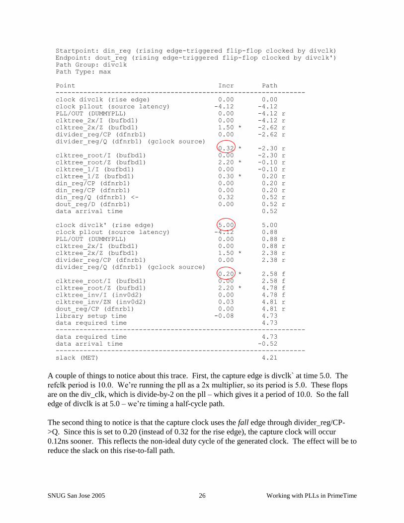
A couple of things to notice about this trace. First, the capture edge is divclk` at time 5.0. The
refclk period is 10.0. We’re running the pll as a 2x multiplier, so its period is 5.0. These flops
are on the div_clk, which is divide-by-2 on the pll – which gives it a period of 10.0. So the fall
edge of divclk is at 5.0 – we’re timing a half-cycle path.
The second thing to notice is that the capture clock uses the fall edge through divider_reg/CP-
>Q. Since this is set to 0.20 (instead of 0.32 for the rise edge), the capture clock will occur
0.12ns sooner. This reflects the non-ideal duty cycle of the generated clock. The effect will be to
reduce the slack on this rise-to-fall path.

SNUG San Jose 2005 Working with PLLs in PrimeTime 27
The important thing to notice, however, is that the duty cycle effect is handled automatically by
the tool.
3.2 Primary input clocks and PLLs
Primary input clocks and pll output clocks are not handled automatically by the tool, since it
can’t deduce what the effect would be. You have to tell it via the –waveform option on
create_clock. But there’s a snag. The incoming clock (or the pll output clock) spec doesn’t tell
you that the duty cycle is, say, “55%”. It usually says the duty cycle is, say, 50% +/- 5%. For
internal clocks, the duty cycle is what it is, but for primary input clocks and pll output clocks, it’s
a range.
Let’s take this simple example:
Figure 3-2
This circuit has paths from the rising clock to the falling clock, from the falling clock to the
falling clock, and from the falling clock to the rising clock.
So, how do we model this in PrimeTime? Well, duty cycle seems like an uncertainty, so your
first thought might be to use set_clock_uncertainty. Unfortunately, this command doesn’t allow
you to set uncertainty between the rising and falling edges of the same clock. It has the –rise_to,
-fall_from options, but the man page says you can only use this for inter-clock uncertainty – that
is, uncertainty between two clocks.
<added 3/17/2005>
The man page says:
-from from_clock -to to_clock
These two options specify the source and
destination clocks for interclock
uncertainty. You must specify either
the pair of -from/-rise_from/-fall_from
and -to/-rise_to/-fall_to, or
object_list; you cannot specify both.
Formatted: Font: Bold

SNUG San Jose 2005 Working with PLLs in PrimeTime 28
…
-fall Indicates that uncertainty applies to
only the falling edge of the destination
clock. By default, the uncertainty
applies to both rising and falling
edges. This option is valid only for
interclock uncertainty, and is now
obsolete. Unless you need this option
for backward-compatibility, use -fall_to
instead.
Sure enough, if you try to use edge switches with intraclock uncertainty, you get an error:
pt_shell> set_clock_uncertainty -setup -rise 0.2 [get_clocks clkin]
Error: Cannot specify '-rise or -fall' with 'clock_list'. (CMD-001)
0
But PT will accept this:
pt_shell> set_clock_uncertainty -setup -rise_from [get_clocks clkin] -fall_to [get_clocks
clkin] 0.2
1
So, it appears that you can specify single-edge uncertainty intra-clock by using the inter-
clock syntax. The man page doesn’t say you can’t make both clocks in the inter-clock
syntax be the same.
It appears to work:
pt_shell> report_timing -from din_reg -to dout_reg
****************************************
Report : timing
-path full
-delay max
-max_paths 1
Design : simple
Version: W-2004.12-SP1
Date : Thu Mar 17 18:26:54 2005
****************************************
Warning: There are 3 invalid start points. (UITE-416)
Warning: There are 2 invalid end points for constrained paths. (UITE-416)
Startpoint: din_reg (rising edge-triggered flip-flop clocked by clkin)
Endpoint: dout_reg (rising edge-triggered flip-flop clocked by clkin')
Path Group: clkin
Path Type: max
Point Incr Path
---------------------------------------------------------------
Formatted: Font: Bold, Italic
Formatted: Font: Bold
Formatted: Font: Courier New, 10 pt, Bold

SNUG San Jose 2005 Working with PLLs in PrimeTime 29
clock clkin (rise edge) 0.00 0.00
clock network delay (propagated) 0.00 0.00
din_reg/CP (dfnrb1) 0.00 0.00 r
din_reg/Q (dfnrb1) <- 0.31 0.31 r
dout_reg/D (dfnrb1) 0.00 0.31 r
data arrival time 0.31
clock clkin' (rise edge) 5.00 5.00
clock network delay (propagated) 0.02 5.02
inter-clock uncertainty -0.20 4.82
dout_reg/CP (dfnrb1) 4.82 r
library setup time -0.09 4.73
data required time 4.73
---------------------------------------------------------------
data required time 4.73
data arrival time -0.31
---------------------------------------------------------------
slack (MET) 4.42
Still, there are disadvantages to this approach. Rolling the duty cycle into
uncertainty will make it difficult to separate duty cycle issues from other
uses of set_clock_uncertainty described later.
On the other hand, the uncertainty method may have some advantages in runtime
(fewer clocks) and possibly in SI analysis over the technique described below.
It is possible to model duty cycle using “set_clock_latency –fall”, but it doesn’t work out-of-the-
box. You have to (ab)use some of the on-chip-variation features for something unrelated to on-
chip-variation, and isn’t too clean (it is explained in Appendix [10.3/4]).
Until a few years ago, there seemed to be no really clean way to model this except to run the
script twice – once for each of the extreme duty cycle waveforms (I call them min_high and
max_high). With the introduction of multiclock propagation capabilities in PT, we can now do
this in a single run.
Since we are going to use multiclock propagation, we first need to turn it on (it’s off by default):
set timing_enable_multiple_clocks_per_reg true
Formatted: Font: Courier New, 10 pt, Bold,Norwegian, Bokmål (Norway)
Formatted: Font: Courier New, 10 pt, Bold
Formatted: Font: Bold
Formatted: Font: Courier New, 10 pt
SNUG San Jose 2005 Working with PLLs in PrimeTime 30
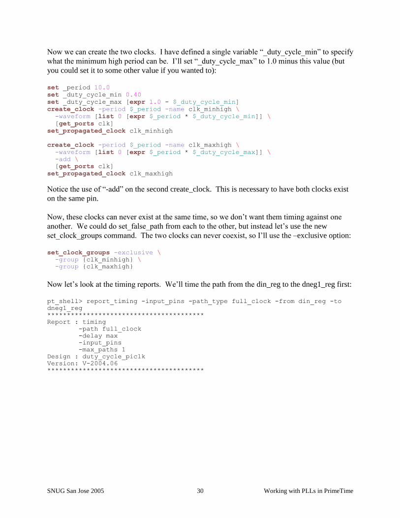
Now we can create the two clocks. I have defined a single variable “_duty_cycle_min” to specify
what the minimum high period can be. I’ll set “_duty_cycle_max” to 1.0 minus this value (but
you could set it to some other value if you wanted to):
set _period 10.0
set _duty_cycle_min 0.40
set _duty_cycle_max [expr 1.0 - $_duty_cycle_min]
create_clock -period $_period -name clk_minhigh \
-waveform [list 0 [expr $_period * $_duty_cycle_min]] \
[get_ports clk]
set_propagated_clock clk_minhigh
create_clock -period $_period -name clk_maxhigh \
-waveform [list 0 [expr $_period * $_duty_cycle_max]] \
-add \
[get_ports clk]
set_propagated_clock clk_maxhigh
Notice the use of “-add” on the second create_clock. This is necessary to have both clocks exist
on the same pin.
Now, these clocks can never exist at the same time, so we don’t want them timing against one
another. We could do set_false_path from each to the other, but instead let’s use the new
set_clock_groups command. The two clocks can never coexist, so I’ll use the –exclusive option:
set_clock_groups -exclusive \
-group {clk_minhigh} \
-group {clk_maxhigh}
Now let’s look at the timing reports. We’ll time the path from the din_reg to the dneg1_reg first:
pt_shell> report_timing -input_pins -path_type full_clock -from din_reg -to
dneg1_reg
****************************************
Report : timing
-path full_clock
-delay max
-input_pins
-max_paths 1
Design : duty_cycle_piclk
Version: V-2004.06
****************************************
SNUG San Jose 2005 Working with PLLs in PrimeTime 31
Startpoint: din_reg (rising edge-triggered flip-flop clocked by clk_maxhigh)
Endpoint: dneg1_reg (rising edge-triggered flip-flop clocked by
clk_maxhigh')
Path Group: clk_maxhigh
Path Type: max
Point Incr Path
---------------------------------------------------------------
clock clk_maxhigh (rise edge) 0.00 0.00
clock source latency 0.00 0.00
clk (in) 0.00 0.00 r
din_reg/CP (dfnrb1) 0.00 0.00 r
din_reg/Q (dfnrb1) <- 0.31 * 0.31 r
dneg1_reg/D (dfnrb1) 0.00 0.31 r
data arrival time 0.31
clock clk_maxhigh' (rise edge) 6.00 6.00
clock source latency 0.00 6.00
clk (in) 0.00 6.00 f
clkinv/I (inv0d2) 0.00 6.00 f
clkinv/ZN (inv0d2) 1.00 * 7.00 r
dneg1_reg/CP (dfnrb1) 0.00 7.00 r
library setup time -0.09 6.91
data required time 6.91
---------------------------------------------------------------
data required time 6.91
data arrival time -0.31
---------------------------------------------------------------
slack (MET) 6.60
Startpoint: din_reg (rising edge-triggered flip-flop clocked by clk_minhigh)
Endpoint: dneg1_reg (rising edge-triggered flip-flop clocked by
clk_minhigh')
Path Group: clk_minhigh
Path Type: max
Point Incr Path
---------------------------------------------------------------
clock clk_minhigh (rise edge) 0.00 0.00
clock source latency 0.00 0.00
clk (in) 0.00 0.00 r
din_reg/CP (dfnrb1) 0.00 0.00 r
din_reg/Q (dfnrb1) <- 0.31 * 0.31 r
dneg1_reg/D (dfnrb1) 0.00 0.31 r
data arrival time 0.31
clock clk_minhigh' (rise edge) 4.00 4.00
clock source latency 0.00 4.00
clk (in) 0.00 4.00 f
clkinv/I (inv0d2) 0.00 4.00 f
clkinv/ZN (inv0d2) 1.00 * 5.00 r
dneg1_reg/CP (dfnrb1) 0.00 5.00 r
library setup time -0.09 4.91
data required time 4.91
---------------------------------------------------------------
data required time 4.91
data arrival time -0.31
---------------------------------------------------------------
slack (MET) 4.60
SNUG San Jose 2005 Working with PLLs in PrimeTime 32
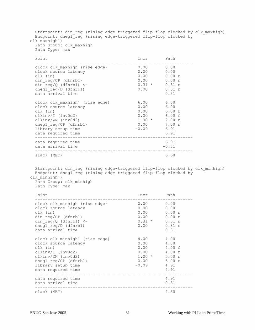
We get two timing reports – one for clk_minhigh and one for clk_maxhigh. Since we are
launching data from a rising edge (both clocks have the same rising edge waveform) and
capturing with the falling edge, the worst case for setup is the shorter duty cycle clock –
clk_minhigh. As you can see, clk_minhigh does indeed have less slack. Its fall edge (that weird
“clock clk_minhigh’ (rise edge)” is PT-speak for falling edge) is at time 4.0 – 40% of the 10ns
period.
Next we’ll look at the falling-edge to falling-edge path.
pt_shell> report_timing -input_pins -path_type full_clock -from dneg1_reg -to
dneg2_reg
****************************************
Report : timing
-path full_clock
-delay max
-input_pins
-max_paths 1
Design : duty_cycle_piclk
Version: V-2004.06
****************************************
Startpoint: dneg1_reg (rising edge-triggered flip-flop clocked by
clk_maxhigh')
Endpoint: dneg2_reg (rising edge-triggered flip-flop clocked by
clk_maxhigh')
Path Group: clk_maxhigh
Path Type: max
Point Incr Path
---------------------------------------------------------------
clock clk_maxhigh' (rise edge) 6.00 6.00
clock source latency 0.00 6.00
clk (in) 0.00 6.00 f
clkinv/I (inv0d2) 0.00 6.00 f
clkinv/ZN (inv0d2) 1.00 * 7.00 r
dneg1_reg/CP (dfnrb1) 0.00 7.00 r
dneg1_reg/Q (dfnrb1) <- 0.32 * 7.32 r
dneg2_reg/D (dfnrb1) 0.00 7.32 r
data arrival time 7.32
clock clk_maxhigh' (rise edge) 16.00 16.00
clock source latency 0.00 16.00
clk (in) 0.00 16.00 f
clkinv/I (inv0d2) 0.00 16.00 f
clkinv/ZN (inv0d2) 1.00 * 17.00 r
dneg2_reg/CP (dfnrb1) 0.00 17.00 r
library setup time -0.09 16.91
data required time 16.91
---------------------------------------------------------------
data required time 16.91
data arrival time -7.32
---------------------------------------------------------------
slack (MET) 9.59

SNUG San Jose 2005 Working with PLLs in PrimeTime 33
Startpoint: dneg1_reg (rising edge-triggered flip-flop clocked by
clk_minhigh')
Endpoint: dneg2_reg (rising edge-triggered flip-flop clocked by
clk_minhigh')
Path Group: clk_minhigh
Path Type: max
Point Incr Path
---------------------------------------------------------------
clock clk_minhigh' (rise edge) 4.00 4.00
clock source latency 0.00 4.00
clk (in) 0.00 4.00 f
clkinv/I (inv0d2) 0.00 4.00 f
clkinv/ZN (inv0d2) 1.00 * 5.00 r
dneg1_reg/CP (dfnrb1) 0.00 5.00 r
dneg1_reg/Q (dfnrb1) <- 0.32 * 5.32 r
dneg2_reg/D (dfnrb1) 0.00 5.32 r
data arrival time 5.32
clock clk_minhigh' (rise edge) 14.00 14.00
clock source latency 0.00 14.00
clk (in) 0.00 14.00 f
clkinv/I (inv0d2) 0.00 14.00 f
clkinv/ZN (inv0d2) 1.00 * 15.00 r
dneg2_reg/CP (dfnrb1) 0.00 15.00 r
library setup time -0.09 14.91
data required time 14.91
---------------------------------------------------------------
data required time 14.91
data arrival time -5.32
---------------------------------------------------------------
slack (MET) 9.59
Again, there are two traces, one for each clock. Although the launch and capture times are
different, as you would expect, the slack values are the same.
Now let’s look at the dneg2_reg to dout_reg path:
pt_shell> report_timing -input_pins -path_type full_clock -from dneg2_reg -to
dout_reg
****************************************
Report : timing
-path full_clock
-delay max
-input_pins
-max_paths 1
Design : duty_cycle_piclk
Version: V-2004.06
****************************************

SNUG San Jose 2005 Working with PLLs in PrimeTime 34
Startpoint: dneg2_reg (rising edge-triggered flip-flop clocked by
clk_maxhigh')
Endpoint: dout_reg (rising edge-triggered flip-flop clocked by clk_maxhigh)
Path Group: clk_maxhigh
Path Type: max
Point Incr Path
---------------------------------------------------------------
clock clk_maxhigh' (rise edge) 6.00 6.00
clock source latency 0.00 6.00
clk (in) 0.00 6.00 f
clkinv/I (inv0d2) 0.00 6.00 f
clkinv/ZN (inv0d2) 1.00 * 7.00 r
dneg2_reg/CP (dfnrb1) 0.00 7.00 r
dneg2_reg/Q (dfnrb1) <- 0.32 * 7.32 r
dout_reg/D (dfnrb1) 0.00 7.32 r
data arrival time 7.32
clock clk_maxhigh (rise edge) 10.00 10.00
clock source latency 0.00 10.00
clk (in) 0.00 10.00 r
dout_reg/CP (dfnrb1) 0.00 10.00 r
library setup time -0.10 9.90
data required time 9.90
---------------------------------------------------------------
data required time 9.90
data arrival time -7.32
---------------------------------------------------------------
slack (MET) 2.58
Since this is from the falling edge to the rising edge, the worst case path will be from the later
falling edge, which is clk_maxhigh. There is another trace for clk_minhigh with 2 more ns of
slack.
So, we can model duty cycle variation in a single pass using two “exclusive” clocks and
multiclock propagation.
3.3 Applying this to our multiplier pll circuit
We can use this on our multiplier pll circuit in 2 places – the primary input clock clkin and the pll
clock pllout.

SNUG San Jose 2005 Working with PLLs in PrimeTime 35
We’ll use the same circuit as before, except that I have added a pair of flops on the pllout clock,
one rising edge and the other falling edge, to illustrate the duty cycle effect on pllout clock.
Figure 3-3
First we’ll create the primary input clocks, one for each duty cycle case. We’ll use a loop.
set _period 10.0
set _duty_cycle(min) 0.40
set _duty_cycle(max) [expr 1.0 - $_duty_cycle(min)]
foreach _dc {min max} {
create_clock -period $_period -name clkin_${_dc}high \
-waveform [list 0 [expr $_period * $_duty_cycle($_dc)]] \
-add \
[get_ports clkin]
set_propagated_clock clkin_${_dc}high
}
set_clock_groups -exclusive \
-group {clkin_minhigh} \
-group {clkin_maxhigh}
Notice the “-add” switch again. Since the create_clock is done in a loop, the –add will occur on
both create_clock commands, including the first one. This is harmless.
Duty Cycle 50% +/- 10%
Duty Cycle 50% +/- 10%

SNUG San Jose 2005 Working with PLLs in PrimeTime 36
Creating the pll output clocks is similar:
set _period [expr 10.0 / 2]
set _duty_cycle(min) 0.40
set _duty_cycle(max) [expr 1.0 - $_duty_cycle(min)]
foreach _dc {min max} {
create_clock -period $_period -name pllout_${_dc}high \
-waveform [list 0 [expr $_period * $_duty_cycle($_dc)]] \
-add \
[get_pins PLL/OUT]
set_propagated_clock pllout_${_dc}high
}
set_clock_groups -exclusive \
-group {pllout_minhigh} \
-group {pllout_maxhigh}
Now we need to create the generated divider clock. But now there are two clocks feeding the
divider_reg/CP pin. Which do we choose, and how do we tell PT about our choice?
Well, in this case, the choice is arbitrary. Since divider_reg only runs on rising edges, it doesn’t
matter which pllout_ clock we choose. If divider_reg ran on falling edges, however, we would
have to create two generated clocks – one for pllout_minhigh and one for pllout_maxhigh. We
would then add these to their respective clock groups in set_clock_group. In fact, we could still
do this even though divider_reg runs on rising edges – the propagated clocks would be identical,
but this is harmless. Some would argue that this is more consistent. It’s is a personal choice.
To keep things simple, we’ll just create one generated clock. We’ll use pllout_maxhigh.
When multiple clocks feed into a point where we want to create a generated clock, it is necessary
to tell PT which clock is the source. This is done using the “-master” switch. To use the “-
master” switch, you must also use the “-add” switch, even though we’re only creating one clock.
create_generated_clock \
-source [get_pins PLL/OUT] \
-name divclk \
-divide_by 2 \
-add \
-master pllout_maxhigh \
[get_pins divider_reg/Q]
set_propagated_clock divclk
SNUG San Jose 2005 Working with PLLs in PrimeTime 37
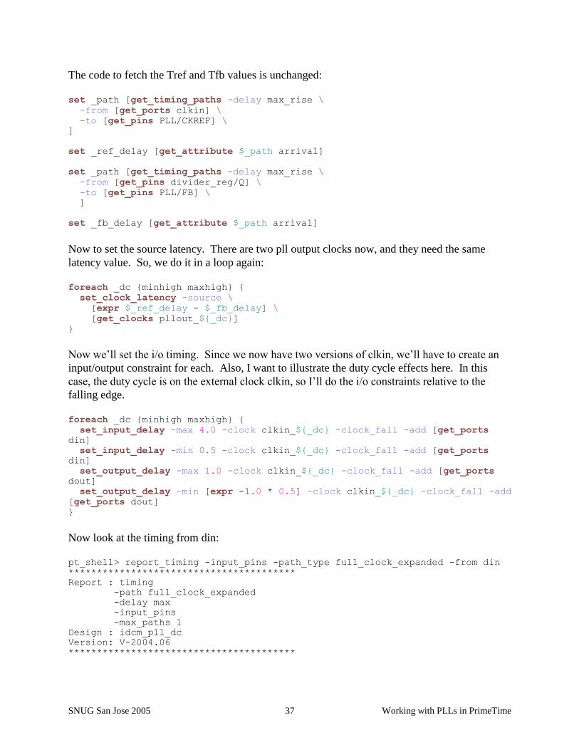
The code to fetch the Tref and Tfb values is unchanged:
set _path [get_timing_paths -delay max_rise \
-from [get_ports clkin] \
-to [get_pins PLL/CKREF] \
]
set _ref_delay [get_attribute $_path arrival]
set _path [get_timing_paths -delay max_rise \
-from [get_pins divider_reg/Q] \
-to [get_pins PLL/FB] \
]
set _fb_delay [get_attribute $_path arrival]
Now to set the source latency. There are two pll output clocks now, and they need the same
latency value. So, we do it in a loop again:
foreach _dc {minhigh maxhigh} {
set_clock_latency -source \
[expr $_ref_delay - $_fb_delay] \
[get_clocks pllout_${_dc}]
}
Now we’ll set the i/o timing. Since we now have two versions of clkin, we’ll have to create an
input/output constraint for each. Also, I want to illustrate the duty cycle effects here. In this
case, the duty cycle is on the external clock clkin, so I’ll do the i/o constraints relative to the
falling edge.
foreach _dc {minhigh maxhigh} {
set_input_delay -max 4.0 -clock clkin_${_dc} -clock_fall -add [get_ports
din]
set_input_delay -min 0.5 -clock clkin_${_dc} -clock_fall -add [get_ports
din]
set_output_delay -max 1.0 -clock clkin_${_dc} -clock_fall -add [get_ports
dout]
set_output_delay -min [expr -1.0 * 0.5] -clock clkin_${_dc} -clock_fall -add
[get_ports dout]
}
Now look at the timing from din:
pt_shell> report_timing -input_pins -path_type full_clock_expanded -from din
****************************************
Report : timing
-path full_clock_expanded
-delay max
-input_pins
-max_paths 1
Design : idcm_pll_dc
Version: V-2004.06
****************************************
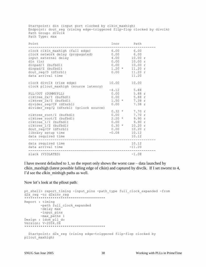
SNUG San Jose 2005 Working with PLLs in PrimeTime 38
Startpoint: din (input port clocked by clkin_maxhigh)
Endpoint: dout_reg (rising edge-triggered flip-flop clocked by divclk)
Path Group: divclk
Path Type: max
Point Incr Path
---------------------------------------------------------------
clock clkin_maxhigh (fall edge) 6.00 6.00
clock network delay (propagated) 0.00 6.00
input external delay 4.00 10.00 r
din (in) 0.00 10.00 r
dinpad/I (bufbd1) 0.00 10.00 r
dinpad/Z (bufbd1) 1.20 * 11.20 r
dout_reg/D (dfnrb1) 0.00 11.20 r
data arrival time 11.20
clock divclk (rise edge) 10.00 10.00
clock pllout_maxhigh (source latency)
-4.12 5.88
PLL/OUT (DUMMYPLL) 0.00 5.88 r
clktree_2x/I (bufbd1) 0.00 5.88 r
clktree_2x/Z (bufbd1) 1.50 * 7.38 r
divider_reg/CP (dfnrb1) 0.00 7.38 r
divider_reg/Q (dfnrb1) (gclock source)
0.32 * 7.70 r
clktree_root/I (bufbd1) 0.00 7.70 r
clktree_root/Z (bufbd1) 2.20 * 9.90 r
clktree_1/I (bufbd1) 0.00 9.90 r
clktree_1/Z (bufbd1) 0.30 * 10.20 r
dout_reg/CP (dfnrb1) 0.00 10.20 r
library setup time -0.08 10.12
data required time 10.12
---------------------------------------------------------------
data required time 10.12
data arrival time -11.20
---------------------------------------------------------------
slack (VIOLATED) -1.08
I have nworst defaulted to 1, so the report only shows the worst case – data launched by
clkin_maxhigh (latest possible falling edge of clkin) and captured by divclk. If I set nworst to 4,
I’d see the clkin_minhigh paths as well.
Now let’s look at the pllout path:
pt_shell> report_timing -input_pins -path_type full_clock_expanded -from
d2x_reg -to d2xinv_reg
****************************************
Report : timing
-path full_clock_expanded
-delay max
-input_pins
-max_paths 1
Design : idcm_pll_dc
Version: V-2004.06
****************************************
Startpoint: d2x_reg (rising edge-triggered flip-flop clocked by
pllout_maxhigh)

SNUG San Jose 2005 Working with PLLs in PrimeTime 39
Endpoint: d2xinv_reg (rising edge-triggered flip-flop clocked by
pllout_maxhigh')
Path Group: pllout_maxhigh
Path Type: max
Point Incr Path
---------------------------------------------------------------
clock pllout_maxhigh (rise edge) 0.00 0.00
clock source latency -4.12 -4.12
PLL/OUT (DUMMYPLL) 0.00 -4.12 r
clktree_2x/I (bufbd1) 0.00 -4.12 r
clktree_2x/Z (bufbd1) 1.50 * -2.62 r
d2x_reg/CP (dfnrb1) 0.00 -2.62 r
d2x_reg/Q (dfnrb1) <- 0.34 -2.28 r
d2xinv_reg/D (dfnrb1) 0.00 -2.28 r
data arrival time -2.28
clock pllout_maxhigh' (rise edge) 3.00 3.00
clock source latency -4.12 -1.12
PLL/OUT (DUMMYPLL) 0.00 -1.12 f
clktree_2x/I (bufbd1) 0.00 -1.12 f
clktree_2x/Z (bufbd1) 1.50 * 0.38 f
clktree_2xinv/I (inv0d2) 0.00 0.38 f
clktree_2xinv/ZN (inv0d2) 0.04 0.42 r
d2xinv_reg/CP (dfnrb1) 0.00 0.42 r
library setup time -0.08 0.33
data required time 0.33
---------------------------------------------------------------
data required time 0.33
data arrival time 2.28
---------------------------------------------------------------
slack (MET) 2.61
Startpoint: d2x_reg (rising edge-triggered flip-flop clocked by
pllout_minhigh)
Endpoint: d2xinv_reg (rising edge-triggered flip-flop clocked by
pllout_minhigh')
Path Group: pllout_minhigh
Path Type: max
Point Incr Path
---------------------------------------------------------------
clock pllout_minhigh (rise edge) 0.00 0.00
clock source latency -4.12 -4.12
PLL/OUT (DUMMYPLL) 0.00 -4.12 r
clktree_2x/I (bufbd1) 0.00 -4.12 r
clktree_2x/Z (bufbd1) 1.50 * -2.62 r
d2x_reg/CP (dfnrb1) 0.00 -2.62 r
d2x_reg/Q (dfnrb1) <- 0.34 -2.28 r
d2xinv_reg/D (dfnrb1) 0.00 -2.28 r
data arrival time -2.28
clock pllout_minhigh' (rise edge) 2.00 2.00
clock source latency -4.12 -2.12
PLL/OUT (DUMMYPLL) 0.00 -2.12 f
clktree_2x/I (bufbd1) 0.00 -2.12 f
clktree_2x/Z (bufbd1) 1.50 * -0.62 f
clktree_2xinv/I (inv0d2) 0.00 -0.62 f
clktree_2xinv/ZN (inv0d2) 0.04 -0.58 r
d2xinv_reg/CP (dfnrb1) 0.00 -0.58 r
SNUG San Jose 2005 Working with PLLs in PrimeTime 40
library setup time -0.08 -0.67
data required time -0.67
---------------------------------------------------------------
data required time -0.67
data arrival time 2.28
---------------------------------------------------------------
slack (MET) 1.61
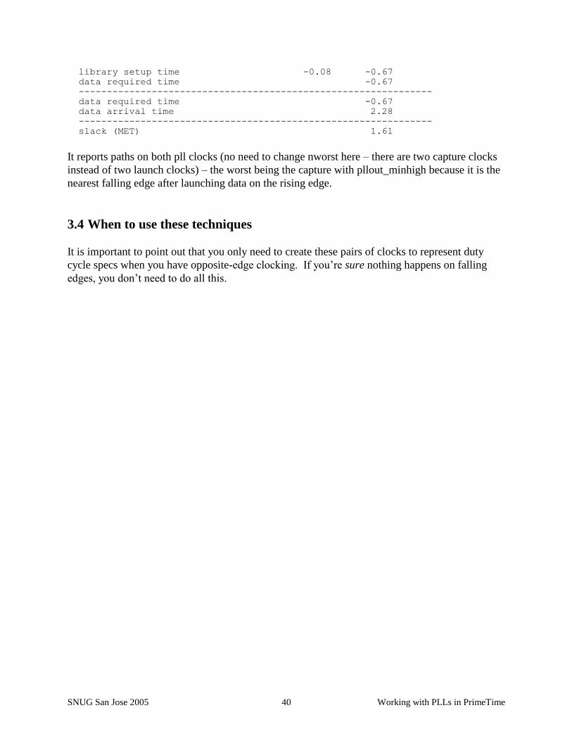
It reports paths on both pll clocks (no need to change nworst here – there are two capture clocks
instead of two launch clocks) – the worst being the capture with pllout_minhigh because it is the
nearest falling edge after launching data on the rising edge.
3.4 When to use these techniques
It is important to point out that you only need to create these pairs of clocks to represent duty
cycle specs when you have opposite-edge clocking. If you’re sure nothing happens on falling
edges, you don’t need to do all this.

SNUG San Jose 2005 Working with PLLs in PrimeTime 41
4 Jitter
4.1 Jitter, skew, and uncertainty
I don’t know if there are any “official” definitions of jitter and skew. I tend to think of jitter as a
high-frequency, cycle-to-cycle phenomenon. I tend to think of skew as something static or at
least very slow-changing. But there is one type of “skew” that I want to discuss up front – clock
tree skew.
Clock tree skew is the difference in delays from the clock source to the various flop clock pins on
the clock network. Because clock tree skew is often modeled in synthesis as clock uncertainty, it
has come to be associated in many people’s minds with all the other things that are modeled
using clock uncertainty. However, for post-route analysis (which is what is being addressed in
this paper), clock tree skew doesn’t exist as a separate entity and does not need to be modeled. It
is already there in the delay numbers or parasitics. For post-route analysis, any skew in the clock
tree will automatically be handled by PT – it knows the exact delay to each element on the clock
tree and will do slack calculations using these numbers. There is no need to budget for clock tree
skew.
There is also a phenomenon that I would call “clock tree jitter”. Since switching thresholds and
delay can vary slightly according to switching activity in other gates, there may indeed be more
cycle-to-cycle jitter at the end of the clock tree than there was at the beginning. I have seen this
in an actual chip – a heavily loaded divide-by 2 clock was “modulating” the faster clock. Every
time the slow clock switched from low to high, a lot of current was drawn, and the faster clock’s
edge rate would slow down, thus delaying the faster clock. This caused a fairly pronounced
cycle-to-cycle jitter at the end of the fast clock tree. This is admittedly a somewhat extreme case,
but we may someday have to account for “clock tree jitter” in our analysis.
4.2 My definition of jitter
There doesn’t seem to be a common interpretation of what a jitter specification means. I’m
going to define jitter somewhat loosely as follows:
“Jitter is the maximum/minimum variation in the length of a single clock cycle”.
This means that a 10ns clock with jitter of +/-100ps can have a minimum cycle length of 9.9ns
and a maximum cycle length of 10.1ns.
This is not the only possible definition of jitter. You can also define jitter as “the uncertainty in
the location of a clock edge relative to its nominal location”. By this definition, our 10ns clock
with +/-100ps jitter can actually have a minimum period of 9.8 and a maximum period of 10.2
(jitter edge late followed by jitter edge early and jitter edge early followed by jitter edge late). Or
you could define our original clock (period 9.9 to 10.1) as having edge jitter of +/-50ps.

SNUG San Jose 2005 Working with PLLs in PrimeTime 42
These two different definitions stem from two different sources of jitter. The “cycle” definition
represents “frequency” jitter – like a PLL adjusting its cycle to track a source. The “edge”
definition represents “noise” jitter – switching thresholds and the like that cause uncertainty
against a steady frequency.
Both types of jitter may be real. In most cases, you can convert “noise” jitter to an equivalent 2x
value and add it to the “frequency” jitter to get cycle jitter (which is what I’m using here).
Whenever you divide the clock in some way, this isn’t so clean. More on this later (see the
section on jitter and generated clocks later in this chapter).
4.3 Sources of jitter
There are several sources of jitter related to the pll:. They are:
1. PLL cycle-to-cycle jitter. This is the change in period of the PLL on a cycle-to-cycle
basis.
2. Refclk cycle-to-cycle jitter. This is the change in period of the Refclk on a cycle-to-cycle
basis.
3. PLL phase error. The job of the pll is to make the Fb pin match the Ref pin in phase and
frequency. But the pll is not perfect. Depending on process, temperature, etc there may
be some small difference between the arrival time at the Ref pin and at the Fb pin. Pll
phase error is the measure of this difference.
Pll phase error isn’t technically a form a jitter, but I have included it because it is modeled in the
same way.
4.4 Effects of jitter on different sorts of paths
When modeling jitter effects in PT, it is important to consider the effect of different types of jitter
on different paths.
First, consider the simple case of two flops on a single clock:
Figure 4-1

SNUG San Jose 2005 Working with PLLs in PrimeTime 43
Once we select an arbitrary time zero for the first edge, here are two possibilities for the second
clock edge – early and late.
Figure 4-2
It’s easy to see that the worst-case setup is affected by the jitter. If the clock jitters by +/- 100ps,
that means that the capture clock could be 100ps earlier or 100ps later. Later won’t matter (for
setup), but earlier will reduce the available clock period and therefore reduce the path slack.
Pll cycle-to-cycle jitter will not, however, affect hold paths within the PLL’s clock tree. This is
because hold is a “single-edge” or “same-edge” phenomenon. The question is whether a source
flop will change its data too soon to avoid being captured by the capture flop on the same edge.
If the next edge jitters, it won’t affect hold.
However, hold paths between the pll clock and another clock (like the refclk) will be affected by
the PLL’s cycle-to-cycle jitter.
Here’s an example circuit and waveforms to illustrate this:
Figure 4-3
Clkin jitters late
Clkin jitters early Worst setup

SNUG San Jose 2005 Working with PLLs in PrimeTime 44
Figure 4-4
Although the path uses clocks that are nominally the “same edge” they are really not the same
edge. They are really edges of two different clocks that are supposed to occur at the same time.
But the “at the same time” is affected by jitter. A flop clocked by the pll could in fact launch its
data earlier due to the PLL’s cycle-to-cycle jitter without there being any matching movement of
the capture clock (refclk). It’s easy to see from the above waveform that both setup and hold
margins will be reduced by the sum of the jitters of both clocks.
Now consider pll phase error. Unlike jitter, pll phase error doesn’t affect edge-to-edge timing at
all. It is simply a time shift relative to some arbitrary external standard. Thus, it has absolutely
no effect on internal paths within the PLL’s clock tree. If the pll clock is shifted from the refclk
by 100ps or 100seconds, it won’t matter to flops along the PLL’s clock tree for either setup or
hold.
But pll phase error will certainly affect paths between the pll clock and the ref clock, just as if it
were pll cycle-to-cycle jitter:
clkin early/late
clkin late/early
pllout early/late
pllout late/early
Worst hold
Worst setup

SNUG San Jose 2005 Working with PLLs in PrimeTime 45
Figure 4-5
Here is a table summarizing which type of jitter affects which paths:
Type of
jitter
Same-clock
setup
Same-clock
hold
Refclk
to/from
pllclk setup
Refclk
to/from
pllclk hold
Pll cycle-to-
cycle
Yes No Yes Yes
Refclk
cycle-to
cycle
Yes No Yes Yes
Pll phase
error
No No Yes Yes
Figure 4-6
clkin early/late
clkin late/early
pllout early/late
pllout late/early
Worst hold
Phase offset late
((+)
Setup margin reduced by : clkin_c2cjitter(+) + phase_offset(-) + pll_c2cjitter(-)
Hold margin reduced by : clkin_c2cjitter(-) + phase_offset(+) + pll_c2cjitter(+)
pllout early/late
pllout late/early
Worst setup
Phase offset early

SNUG San Jose 2005 Working with PLLs in PrimeTime 46
Note that I have used a very simplified definition of jitter in these examples. It might be worse
than this. If you allow the refclock to have its maximum jitter for N cycles, and the pll clock to
have its maximum jitter for M consecutive cycles, then you get setup/hold reductions of:
N*refclk_max_jitter + M*pllclk_max_jitter (where “max_jitter” means the max excursion from
nominal – 100ps for a jitter of +/- 100ps). Ultimately this will have to be limited by the “long-
term jitter” spec. If we define “long term jitter” as “the absolute maximum difference between
the edges of the refclk and the pll clock under any and all circumstances”, then perhaps we
should replace the “refclk_c2c_jitter + pllclk_c2c_jitter + phase_error” with a single term – the
long-term jitter. Or, since the long-term jitter spec was probably derived using a jitter-free
reference clock, perhaps the correct answer is “refclk_c2c_jitter + pll_long_term_jitter”.
Of course, we’re not free to define any of these terms. What matters is how the PLL designer
defines them. Since there is, as far as I can tell, no clear industry-accepted definition of jitter
specs, it is important to know what the person who created the spec meant.
The important point to remember is that the uncertainty between the ref clock and the pll clock is
different from the uncertainty of the pll clock itself, and of the ref clock itself. You’ll have to
work with the PLL designer to make sure you get the correct inter-clock value.
4.5 Modeling jitter with set_clock_uncertainty
The PT command “set_clock_uncertainty” is really like two commands rolled into one. It can
really be used only in one of two modes – setting uncertainty within a clock and setting
uncertainty between clocks. Many of the options, in particular the edge-related options, only
apply in inter-clock mode. Different values can be assigned for setup and hold uncertainty.
Looking at the tables above, it is pretty easy to figure out what values to use for the various
uncertainties. For intra-clock (same clock) uncertainties, setup will use the cycle-to-cycle jitter
spec for that clock (the “+/-“ value, or half of the total range). Hold uncertainty will use zero.
For inter-clock uncertainties between the refclk and the pll clock, setup will use the sum of all
three jitter sources, as will hold.
4.6 Applying jitter specs to the example circuit – simple case
First we’ll apply this to the simple case – no divider in the feedback path and no duty cycle
checks. This circuit is just like the one in section 2.2, except that I have added another flop in the
data path to show internal path timing checks.

SNUG San Jose 2005 Working with PLLs in PrimeTime 47
Figure 4-7
Here are the jitters specs we’re going to use:
# Jitter specs
set _pll_c2cjitter 0.200 ;# +/- 0.200
set _phase_error 0.150 ;# +/- 0.150
set _refclk_c2cjitter 0.120 ;# +/- 0.120
After doing all the clock creation and setting the correct source latency as before, we can set the
jitter. First we’ll do the intra-clock uncertainty. Although the hold value would default to 0
anyway, I will set it here to make it clear that 0 is what I want:
# refclk internal
set_clock_uncertainty \
-setup $_refclk_c2cjitter \
[get_clocks clkin]
set_clock_uncertainty \
-hold 0 \
[get_clocks clkin]
# pllout internal
set_clock_uncertainty \
-setup $_pll_c2cjitter \
[get_clocks pllout]
set_clock_uncertainty \
-hold 0 \
[get_clocks pllout]
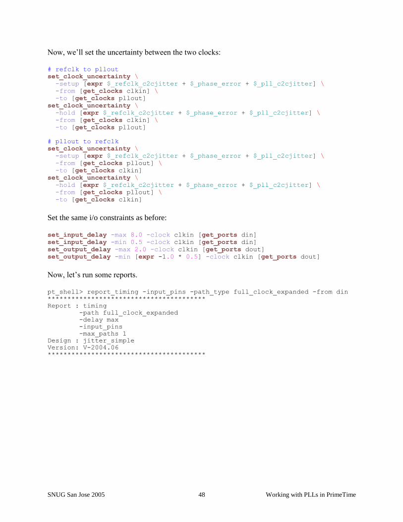
SNUG San Jose 2005 Working with PLLs in PrimeTime 48
Now, we’ll set the uncertainty between the two clocks:
# refclk to pllout
set_clock_uncertainty \
-setup [expr $_refclk_c2cjitter + $_phase_error + $_pll_c2cjitter] \
-from [get_clocks clkin] \
-to [get_clocks pllout]
set_clock_uncertainty \
-hold [expr $_refclk_c2cjitter + $_phase_error + $_pll_c2cjitter] \
-from [get_clocks clkin] \
-to [get_clocks pllout]
# pllout to refclk
set_clock_uncertainty \
-setup [expr $_refclk_c2cjitter + $_phase_error + $_pll_c2cjitter] \
-from [get_clocks pllout] \
-to [get_clocks clkin]
set_clock_uncertainty \
-hold [expr $_refclk_c2cjitter + $_phase_error + $_pll_c2cjitter] \
-from [get_clocks pllout] \
-to [get_clocks clkin]
Set the same i/o constraints as before:
set_input_delay -max 8.0 -clock clkin [get_ports din]
set_input_delay -min 0.5 -clock clkin [get_ports din]
set_output_delay -max 2.0 -clock clkin [get_ports dout]
set_output_delay -min [expr -1.0 * 0.5] -clock clkin [get_ports dout]
Now, let’s run some reports.
pt_shell> report_timing -input_pins -path_type full_clock_expanded -from din
****************************************
Report : timing
-path full_clock_expanded
-delay max
-input_pins
-max_paths 1
Design : jitter_simple
Version: V-2004.06
****************************************
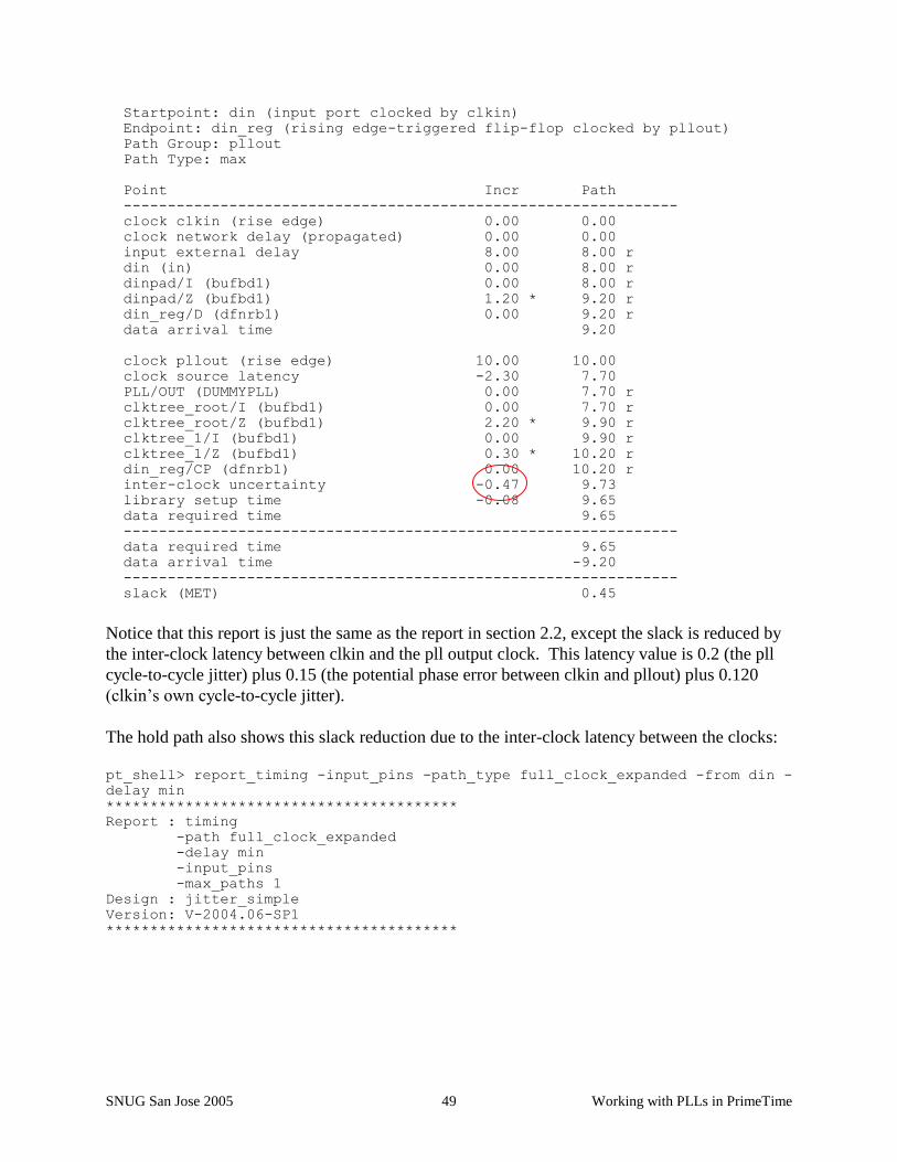
SNUG San Jose 2005 Working with PLLs in PrimeTime 49
Startpoint: din (input port clocked by clkin)
Endpoint: din_reg (rising edge-triggered flip-flop clocked by pllout)
Path Group: pllout
Path Type: max
Point Incr Path
---------------------------------------------------------------
clock clkin (rise edge) 0.00 0.00
clock network delay (propagated) 0.00 0.00
input external delay 8.00 8.00 r
din (in) 0.00 8.00 r
dinpad/I (bufbd1) 0.00 8.00 r
dinpad/Z (bufbd1) 1.20 * 9.20 r
din_reg/D (dfnrb1) 0.00 9.20 r
data arrival time 9.20
clock pllout (rise edge) 10.00 10.00
clock source latency -2.30 7.70
PLL/OUT (DUMMYPLL) 0.00 7.70 r
clktree_root/I (bufbd1) 0.00 7.70 r
clktree_root/Z (bufbd1) 2.20 * 9.90 r
clktree_1/I (bufbd1) 0.00 9.90 r
clktree_1/Z (bufbd1) 0.30 * 10.20 r
din_reg/CP (dfnrb1) 0.00 10.20 r
inter-clock uncertainty -0.47 9.73
library setup time -0.08 9.65
data required time 9.65
---------------------------------------------------------------
data required time 9.65
data arrival time -9.20
---------------------------------------------------------------
slack (MET) 0.45
Notice that this report is just the same as the report in section 2.2, except the slack is reduced by
the inter-clock latency between clkin and the pll output clock. This latency value is 0.2 (the pll
cycle-to-cycle jitter) plus 0.15 (the potential phase error between clkin and pllout) plus 0.120
(clkin’s own cycle-to-cycle jitter).
The hold path also shows this slack reduction due to the inter-clock latency between the clocks:
pt_shell> report_timing -input_pins -path_type full_clock_expanded -from din -
delay min
****************************************
Report : timing
-path full_clock_expanded
-delay min
-input_pins
-max_paths 1
Design : jitter_simple
Version: V-2004.06-SP1
****************************************
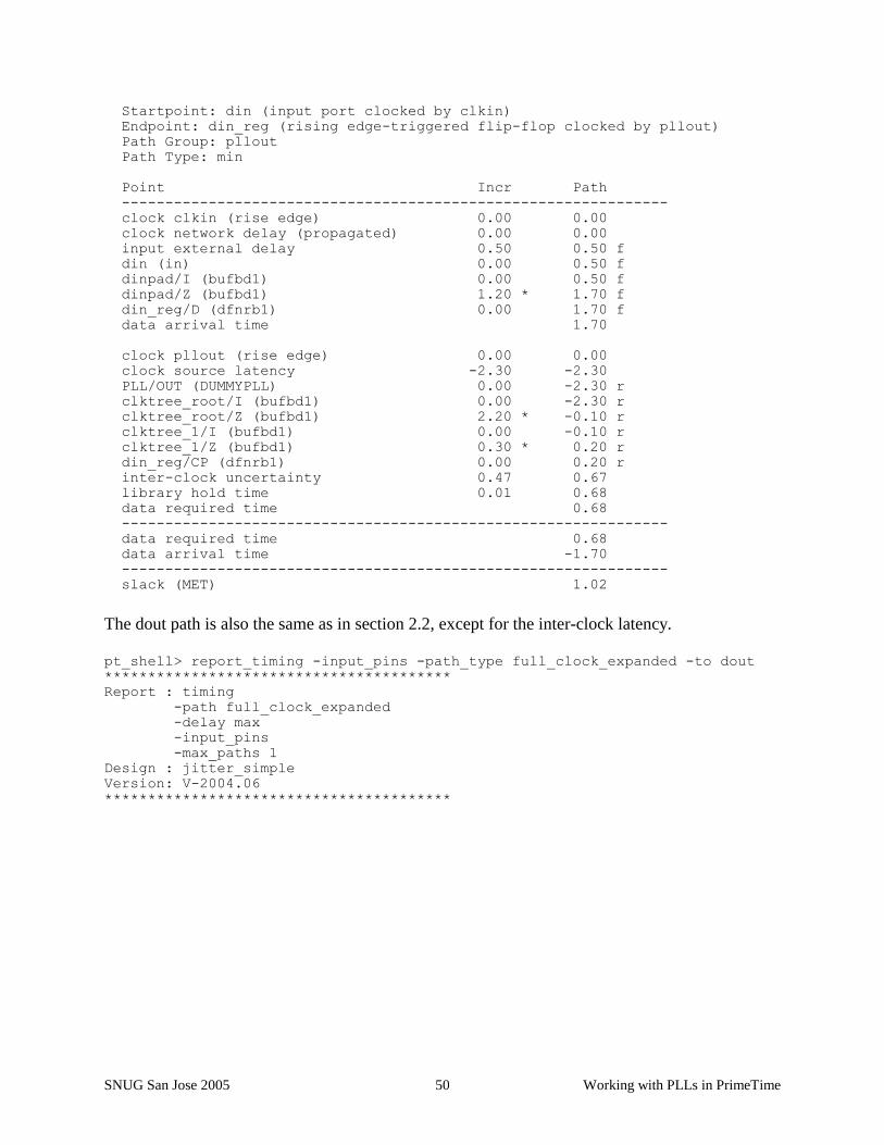
SNUG San Jose 2005 Working with PLLs in PrimeTime 50
Startpoint: din (input port clocked by clkin)
Endpoint: din_reg (rising edge-triggered flip-flop clocked by pllout)
Path Group: pllout
Path Type: min
Point Incr Path
---------------------------------------------------------------
clock clkin (rise edge) 0.00 0.00
clock network delay (propagated) 0.00 0.00
input external delay 0.50 0.50 f
din (in) 0.00 0.50 f
dinpad/I (bufbd1) 0.00 0.50 f
dinpad/Z (bufbd1) 1.20 * 1.70 f
din_reg/D (dfnrb1) 0.00 1.70 f
data arrival time 1.70
clock pllout (rise edge) 0.00 0.00
clock source latency -2.30 -2.30
PLL/OUT (DUMMYPLL) 0.00 -2.30 r
clktree_root/I (bufbd1) 0.00 -2.30 r
clktree_root/Z (bufbd1) 2.20 * -0.10 r
clktree_1/I (bufbd1) 0.00 -0.10 r
clktree_1/Z (bufbd1) 0.30 * 0.20 r
din_reg/CP (dfnrb1) 0.00 0.20 r
inter-clock uncertainty 0.47 0.67
library hold time 0.01 0.68
data required time 0.68
---------------------------------------------------------------
data required time 0.68
data arrival time -1.70
---------------------------------------------------------------
slack (MET) 1.02
The dout path is also the same as in section 2.2, except for the inter-clock latency.
pt_shell> report_timing -input_pins -path_type full_clock_expanded -to dout
****************************************
Report : timing
-path full_clock_expanded
-delay max
-input_pins
-max_paths 1
Design : jitter_simple
Version: V-2004.06
****************************************

SNUG San Jose 2005 Working with PLLs in PrimeTime 51
Startpoint: dout_reg (rising edge-triggered flip-flop clocked by pllout)
Endpoint: dout (output port clocked by clkin)
Path Group: clkin
Path Type: max
Point Incr Path
---------------------------------------------------------------
clock pllout (rise edge) 0.00 0.00
clock source latency -2.30 -2.30
PLL/OUT (DUMMYPLL) 0.00 -2.30 r
clktree_root/I (bufbd1) 0.00 -2.30 r
clktree_root/Z (bufbd1) 2.20 * -0.10 r
clktree_1/I (bufbd1) 0.00 -0.10 r
clktree_1/Z (bufbd1) 0.30 * 0.20 r
dout_reg/CP (dfnrb1) 0.00 0.20 r
dout_reg/Q (dfnrb1) 0.33 0.53 f
doutpad/I (bufbd1) 0.00 0.53 f
doutpad/Z (bufbd1) 2.50 * 3.03 f
dout (out) 0.00 3.03 f
data arrival time 3.03
clock clkin (rise edge) 10.00 10.00
clock network delay (propagated) 0.00 10.00
inter-clock uncertainty -0.47 9.53
output external delay -2.00 7.53
data required time 7.53
---------------------------------------------------------------
data required time 7.53
data arrival time -3.03
---------------------------------------------------------------
slack (MET) 4.50
Here’s the path between the data flops:
pt_shell> report_timing -input_pins -path_type full_clock_expanded -from
din_reg -to dout_reg
****************************************
Report : timing
-path full_clock_expanded
-delay max
-input_pins
-max_paths 1
Design : jitter_simple
Version: V-2004.06
****************************************
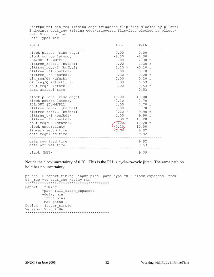
SNUG San Jose 2005 Working with PLLs in PrimeTime 52
Startpoint: din_reg (rising edge-triggered flip-flop clocked by pllout)
Endpoint: dout_reg (rising edge-triggered flip-flop clocked by pllout)
Path Group: pllout
Path Type: max
Point Incr Path
---------------------------------------------------------------
clock pllout (rise edge) 0.00 0.00
clock source latency -2.30 -2.30
PLL/OUT (DUMMYPLL) 0.00 -2.30 r
clktree_root/I (bufbd1) 0.00 -2.30 r
clktree_root/Z (bufbd1) 2.20 * -0.10 r
clktree_1/I (bufbd1) 0.00 -0.10 r
clktree_1/Z (bufbd1) 0.30 * 0.20 r
din_reg/CP (dfnrb1) 0.00 0.20 r
din_reg/Q (dfnrb1) <- 0.33 0.53 r
dout_reg/D (dfnrb1) 0.00 0.53 r
data arrival time 0.53
clock pllout (rise edge) 10.00 10.00
clock source latency -2.30 7.70
PLL/OUT (DUMMYPLL) 0.00 7.70 r
clktree_root/I (bufbd1) 0.00 7.70 r
clktree_root/Z (bufbd1) 2.20 * 9.90 r
clktree_1/I (bufbd1) 0.00 9.90 r
clktree_1/Z (bufbd1) 0.30 * 10.20 r
dout_reg/CP (dfnrb1) 0.00 10.20 r
clock uncertainty -0.20 10.00
library setup time -0.08 9.92
data required time 9.92
---------------------------------------------------------------
data required time 9.92
data arrival time -0.53
---------------------------------------------------------------
slack (MET) 9.39
Notice the clock uncertainty of 0.20. This is the PLL’s cycle-to-cycle jitter. The same path on
hold has no uncertainty:
pt_shell> report_timing -input_pins -path_type full_clock_expanded -from
din_reg -to dout_reg -delay min
****************************************
Report : timing
-path full_clock_expanded
-delay min
-input_pins
-max_paths 1
Design : jitter_simple
Version: V-2004.06
****************************************
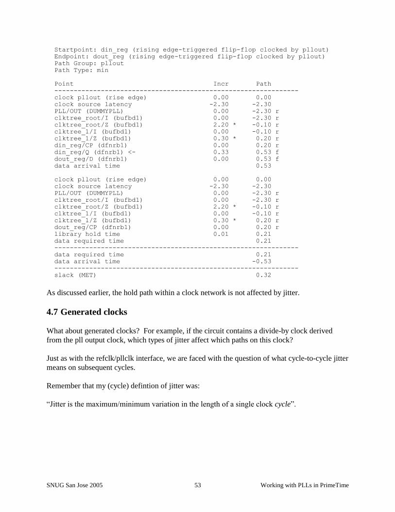
SNUG San Jose 2005 Working with PLLs in PrimeTime 53
Startpoint: din_reg (rising edge-triggered flip-flop clocked by pllout)
Endpoint: dout_reg (rising edge-triggered flip-flop clocked by pllout)
Path Group: pllout
Path Type: min
Point Incr Path
---------------------------------------------------------------
clock pllout (rise edge) 0.00 0.00
clock source latency -2.30 -2.30
PLL/OUT (DUMMYPLL) 0.00 -2.30 r
clktree_root/I (bufbd1) 0.00 -2.30 r
clktree_root/Z (bufbd1) 2.20 * -0.10 r
clktree_1/I (bufbd1) 0.00 -0.10 r
clktree_1/Z (bufbd1) 0.30 * 0.20 r
din_reg/CP (dfnrb1) 0.00 0.20 r
din_reg/Q (dfnrb1) <- 0.33 0.53 f
dout_reg/D (dfnrb1) 0.00 0.53 f
data arrival time 0.53
clock pllout (rise edge) 0.00 0.00
clock source latency -2.30 -2.30
PLL/OUT (DUMMYPLL) 0.00 -2.30 r
clktree_root/I (bufbd1) 0.00 -2.30 r
clktree_root/Z (bufbd1) 2.20 * -0.10 r
clktree_1/I (bufbd1) 0.00 -0.10 r
clktree_1/Z (bufbd1) 0.30 * 0.20 r
dout_reg/CP (dfnrb1) 0.00 0.20 r
library hold time 0.01 0.21
data required time 0.21
---------------------------------------------------------------
data required time 0.21
data arrival time -0.53
---------------------------------------------------------------
slack (MET) 0.32
As discussed earlier, the hold path within a clock network is not affected by jitter.
4.7 Generated clocks
What about generated clocks? For example, if the circuit contains a divide-by clock derived
from the pll output clock, which types of jitter affect which paths on this clock?
Just as with the refclk/pllclk interface, we are faced with the question of what cycle-to-cycle jitter
means on subsequent cycles.
Remember that my (cycle) defintion of jitter was:
“Jitter is the maximum/minimum variation in the length of a single clock cycle”.

SNUG San Jose 2005 Working with PLLs in PrimeTime 54
If you assume that subsequent cycles can also vary by this same amount, at least over the number
of periods concerned, a divide-by N clock can end up with N times the original source clock
jitter. Let’s take the min example (10ns period, +/-100ps jitter):
1x clock Div2 clock Div4 clock
0 0 0
9.9
19.8 19.8
29.7
39.6 39.6 39.6
49.5
59.4 59.4
69.3
79.2 79.2 79.2
If, however, you were to take an edge-centric view of jitter, the uncertainty of any divided clocks
would be the same as the uncertainty of the master clock.
Again, we get back to what the terms mean, and, again, you’ll have to work this out with the PLL
designer. Now let’s look at the various inter- and intra-clock paths related to the generated clock.
We’ll start with paths between the master clock (pll out clock in this case) and the generated
clock. Assuming the path is single-cycle, pll cycle-to-cycle jitter will have no effect on hold for
the same reason it has no effect on hold within the pll clock network – it’s the same edge. Now
consider the setup case (again, assuming a single-cycle path). If the generated clock is the
capture clock, then the data will have been launched one master clock earlier. This launch time
could be late by pll_c2c_jitter, reducing the setup margin by that amount. You cannot
simultaneously pull the capture (generated) clock in because it is directly created by the master
clock. Similarly, if the generated clock is the launch clock, then the next master clock is the
capture clock, and it could be early by pll_c2c_jitter. So, the setup uncertainty for paths between
the master and generated clocks is pll_c2c_jitter.
Pll phase error won’t have any effect on these paths, nor will refclk cycle-to-cycle jitter.
Paths between the refclk and the pll generated clock will be affected in the same way as paths
between the refclk and the pll output clock itself (affected by everything).
Jitter is 2x master clock (200ps)
Jitter is 4x master clock (400ps)
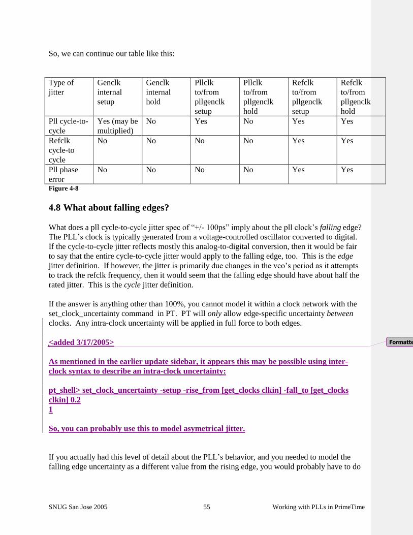
SNUG San Jose 2005 Working with PLLs in PrimeTime 55
So, we can continue our table like this:
Type of
jitter
Genclk
internal
setup
Genclk
internal
hold
Pllclk
to/from
pllgenclk
setup
Pllclk
to/from
pllgenclk
hold
Refclk
to/from
pllgenclk
setup
Refclk
to/from
pllgenclk
hold
Pll cycle-to-
cycle
Yes (may be
multiplied)
No Yes No Yes Yes
Refclk
cycle-to
cycle
No No No No Yes Yes
Pll phase
error
No No No No Yes Yes
Figure 4-8
4.8 What about falling edges?
What does a pll cycle-to-cycle jitter spec of “+/- 100ps” imply about the pll clock’s falling edge?
The PLL’s clock is typically generated from a voltage-controlled oscillator converted to digital.
If the cycle-to-cycle jitter reflects mostly this analog-to-digital conversion, then it would be fair
to say that the entire cycle-to-cycle jitter would apply to the falling edge, too. This is the edge
jitter definition. If however, the jitter is primarily due changes in the vco’s period as it attempts
to track the refclk frequency, then it would seem that the falling edge should have about half the
rated jitter. This is the cycle jitter definition.
If the answer is anything other than 100%, you cannot model it within a clock network with the
set_clock_uncertainty command in PT. PT will only allow edge-specific uncertainty between
clocks. Any intra-clock uncertainty will be applied in full force to both edges.
<added 3/17/2005>
As mentioned in the earlier update sidebar, it appears this may be possible using inter-
clock syntax to describe an intra-clock uncertainty:
pt_shell> set_clock_uncertainty -setup -rise_from [get_clocks clkin] -fall_to [get_clocks
clkin] 0.2
1
So, you can probably use this to model asymetrical jitter.
If you actually had this level of detail about the PLL’s behavior, and you needed to model the
falling edge uncertainty as a different value from the rising edge, you would probably have to do
Formatted: Font: Bold

SNUG San Jose 2005 Working with PLLs in PrimeTime 56
this by adjusting the duty cycle clocks discussed earlier. I’ve never had this level of detail to
work with.
Opposite-edge clocking between the refclk and the pll clock is something I haven’t run into. If
an interface is slow enough to use opposite-edge clocking, it probably doesn’t have an idc pll.
4.9 Applying jitter specs to the example circuit – complex case
Author’s note: If you’re getting a little tired by this point, you might want to skip this section
and go back to it later. It gets a little hairy…
Ok, now let’s try something a little harder. We’ll go back to the 2x multiplier configuration, only
this time I will include some cross-clock paths. And we’ll handle the duty cycle as well.
Figure 4-9
Note: I’m going to assume that the divclk uncertainty is 2 times the pll_c2c_jitter (see discussion
above).
After setting up the clocks (2 primary clocks at clkin, 2 primary clocks at PLL/OUT, and 1
generated clock at divider_reg/Q), and calculating and applying the pll source latency, we’re
ready to apply the uncertainties. We have a total of five clocks, but since the duty cycle clocks
are exclusive to one another, we can treat them as three groups. We’ll set up some collections to
make this easier:
set _pll_clks [get_clocks pllout*high]
set _refclks [get_clocks clkin*high]

SNUG San Jose 2005 Working with PLLs in PrimeTime 57
First, well set the uncertainty for refclk (clkin) internal paths:
set_clock_uncertainty \
-setup $_refclk_c2cjitter \
$_refclks
set_clock_uncertainty \
-hold 0 \
$_refclks
Now we’ll do the paths from refclk to the pll clocks and divclk. They have the same value, so
we can do it in one pair of statements.
set_clock_uncertainty \
-setup [expr $_refclk_c2cjitter + $_phase_error + $_pll_c2cjitter] \
-from $_refclks \
-to [list $_pll_clks [get_clocks divclk] ]
set_clock_uncertainty \
-hold [expr $_refclk_c2cjitter + $_phase_error + $_pll_c2cjitter] \
-from $_refclks \
-to [list $_pll_clks [get_clocks divclk] ]
Now the pll output clk(s) internal paths:
set_clock_uncertainty \
-setup $_pll_c2cjitter \
$_pll_clks
set_clock_uncertainty \
-hold 0 \
$_pll_clks
From pll output clock to divclk is special. It is similar to pll output clock’s internal paths:
set_clock_uncertainty \
-setup $_pll_c2cjitter \
-from $_pll_clks \
-to [get_clocks divclk]
set_clock_uncertainty \
-hold 0 \
-from $_pll_clks \
-to [get_clocks divclk]
Now pll output clocks to refclk:
set_clock_uncertainty \
-setup [expr $_refclk_c2cjitter + $_phase_error + $_pll_c2cjitter] \
-from $_pll_clks \
-to $_refclks
set_clock_uncertainty \
-hold [expr $_refclk_c2cjitter + $_phase_error + $_pll_c2cjitter] \
-from $_pll_clks \
-to $_refclks
And finally we can do divclk itself.

SNUG San Jose 2005 Working with PLLs in PrimeTime 58
First the internal paths. Here’s where we apply the 2x multiplier.
set_clock_uncertainty \
-setup [expr 2 * $_pll_c2cjitter] \
[get_clocks divclk]
set_clock_uncertainty \
-hold 0 \
[get_clocks divclk]
Then the paths to pll output clock (again, similar to internal clocks):
set_clock_uncertainty \
-setup $_pll_c2cjitter \
-from [get_clocks divclk] \
-to $_pll_clks
set_clock_uncertainty \
-hold 0 \
-from [get_clocks divclk] \
-to $_pll_clks
And finally from divclk to refclk:
set_clock_uncertainty \
-setup [expr $_refclk_c2cjitter + $_phase_error + $_pll_c2cjitter] \
-from [get_clocks divclk] \
-to $_refclks
set_clock_uncertainty \
-hold [expr $_refclk_c2cjitter + $_phase_error + $_pll_c2cjitter] \
-from [get_clocks divclk] \
-to $_refclks
Ok, now we set the i/o constraints as before:
foreach _dc {minhigh maxhigh} {
set_input_delay -max 4.0 -clock clkin_${_dc} -add [get_ports din]
set_input_delay -min 0.5 -clock clkin_${_dc} -add [get_ports din]
set_output_delay -max 1.0 -clock clkin_${_dc} -add [get_ports dout]
set_output_delay -min [expr -1.0 * 0.5] -clock clkin_${_dc} -add [get_ports
dout]
}
Here’s the input report:
pt_shell> report_timing -input_pins -path_type full_clock_expanded -from din
****************************************
Report : timing
-path full_clock_expanded
-delay max
-input_pins
-max_paths 1
Design : jitter_example
Version: V-2004.06
****************************************

SNUG San Jose 2005 Working with PLLs in PrimeTime 59
Startpoint: din (input port clocked by clkin_minhigh)
Endpoint: din_reg (rising edge-triggered flip-flop clocked by divclk)
Path Group: divclk
Path Type: max
Point Incr Path
---------------------------------------------------------------
clock clkin_minhigh (rise edge) 0.00 0.00
clock network delay (propagated) 0.00 0.00
input external delay 8.00 8.00 r
din (in) 0.00 8.00 r
dinpad/I (bufbd1) 0.00 8.00 r
dinpad/Z (bufbd1) 1.20 * 9.20 r
din_reg/D (dfnrb1) 0.00 9.20 r
data arrival time 9.20
clock divclk (rise edge) 10.00 10.00
clock pllout_maxhigh (source latency)
-2.61 7.39
PLL/OUT (DUMMYPLL) 0.00 7.39 r
divider_reg/CP (dfnrb1) 0.00 7.39 r
divider_reg/Q (dfnrb1) (gclock source)
0.31 7.70 r
clktree_root/I (bufbd1) 0.00 7.70 r
clktree_root/Z (bufbd1) 2.20 * 9.90 r
clktree_1/I (bufbd1) 0.00 9.90 r
clktree_1/Z (bufbd1) 0.30 * 10.20 r
din_reg/CP (dfnrb1) 0.00 10.20 r
inter-clock uncertainty -0.47 9.73
library setup time -0.08 9.65
data required time 9.65
---------------------------------------------------------------
data required time 9.65
data arrival time -9.20
---------------------------------------------------------------
slack (MET) 0.45
We expect the input and output path slacks to be the same as they were in the last section.
Although now being captured by divclk, the pll will drive divclk with the same timing as the
pllout clock was driven with in the previous example. The source latency and clock path delays
will be different, but the net result will be the same. And it is.
The dout path also matches the previous example.
How about those cross-clock path?. We’ll look at din_reg to d2xout_reg first.
pt_shell> report_timing -input_pins -path_type full_clock_expanded -from
din_reg -to d2xout_reg -delay max
****************************************
Report : timing
-path full_clock_expanded
-delay max
-input_pins
-max_paths 1
Design : jitter_example
Version: V-2004.06
****************************************
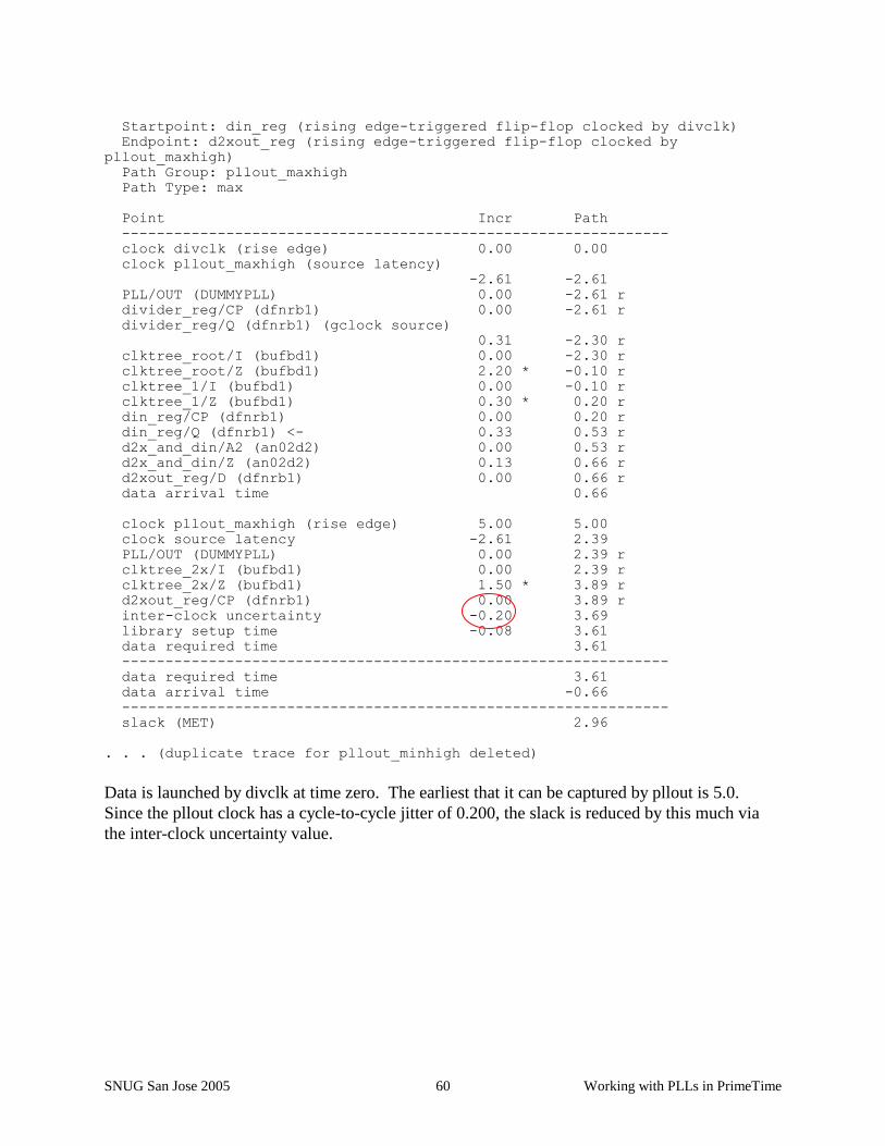
SNUG San Jose 2005 Working with PLLs in PrimeTime 60
Startpoint: din_reg (rising edge-triggered flip-flop clocked by divclk)
Endpoint: d2xout_reg (rising edge-triggered flip-flop clocked by
pllout_maxhigh)
Path Group: pllout_maxhigh
Path Type: max
Point Incr Path
---------------------------------------------------------------
clock divclk (rise edge) 0.00 0.00
clock pllout_maxhigh (source latency)
-2.61 -2.61
PLL/OUT (DUMMYPLL) 0.00 -2.61 r
divider_reg/CP (dfnrb1) 0.00 -2.61 r
divider_reg/Q (dfnrb1) (gclock source)
0.31 -2.30 r
clktree_root/I (bufbd1) 0.00 -2.30 r
clktree_root/Z (bufbd1) 2.20 * -0.10 r
clktree_1/I (bufbd1) 0.00 -0.10 r
clktree_1/Z (bufbd1) 0.30 * 0.20 r
din_reg/CP (dfnrb1) 0.00 0.20 r
din_reg/Q (dfnrb1) <- 0.33 0.53 r
d2x_and_din/A2 (an02d2) 0.00 0.53 r
d2x_and_din/Z (an02d2) 0.13 0.66 r
d2xout_reg/D (dfnrb1) 0.00 0.66 r
data arrival time 0.66
clock pllout_maxhigh (rise edge) 5.00 5.00
clock source latency -2.61 2.39
PLL/OUT (DUMMYPLL) 0.00 2.39 r
clktree_2x/I (bufbd1) 0.00 2.39 r
clktree_2x/Z (bufbd1) 1.50 * 3.89 r
d2xout_reg/CP (dfnrb1) 0.00 3.89 r
inter-clock uncertainty -0.20 3.69
library setup time -0.08 3.61
data required time 3.61
---------------------------------------------------------------
data required time 3.61
data arrival time -0.66
---------------------------------------------------------------
slack (MET) 2.96
. . . (duplicate trace for pllout_minhigh deleted)
Data is launched by divclk at time zero. The earliest that it can be captured by pllout is 5.0.
Since the pllout clock has a cycle-to-cycle jitter of 0.200, the slack is reduced by this much via
the inter-clock uncertainty value.
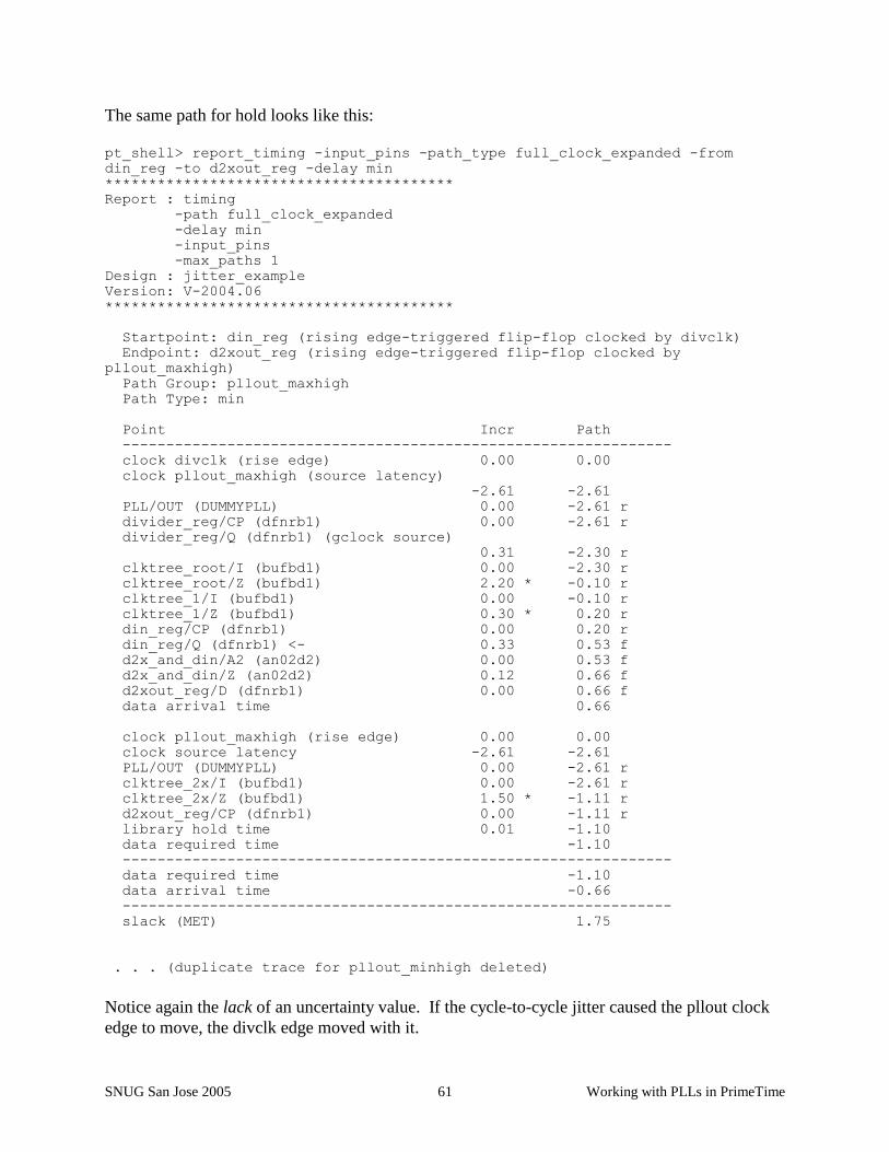
SNUG San Jose 2005 Working with PLLs in PrimeTime 61
The same path for hold looks like this:
pt_shell> report_timing -input_pins -path_type full_clock_expanded -from
din_reg -to d2xout_reg -delay min
****************************************
Report : timing
-path full_clock_expanded
-delay min
-input_pins
-max_paths 1
Design : jitter_example
Version: V-2004.06
****************************************
Startpoint: din_reg (rising edge-triggered flip-flop clocked by divclk)
Endpoint: d2xout_reg (rising edge-triggered flip-flop clocked by
pllout_maxhigh)
Path Group: pllout_maxhigh
Path Type: min
Point Incr Path
---------------------------------------------------------------
clock divclk (rise edge) 0.00 0.00
clock pllout_maxhigh (source latency)
-2.61 -2.61
PLL/OUT (DUMMYPLL) 0.00 -2.61 r
divider_reg/CP (dfnrb1) 0.00 -2.61 r
divider_reg/Q (dfnrb1) (gclock source)
0.31 -2.30 r
clktree_root/I (bufbd1) 0.00 -2.30 r
clktree_root/Z (bufbd1) 2.20 * -0.10 r
clktree_1/I (bufbd1) 0.00 -0.10 r
clktree_1/Z (bufbd1) 0.30 * 0.20 r
din_reg/CP (dfnrb1) 0.00 0.20 r
din_reg/Q (dfnrb1) <- 0.33 0.53 f
d2x_and_din/A2 (an02d2) 0.00 0.53 f
d2x_and_din/Z (an02d2) 0.12 0.66 f
d2xout_reg/D (dfnrb1) 0.00 0.66 f
data arrival time 0.66
clock pllout_maxhigh (rise edge) 0.00 0.00
clock source latency -2.61 -2.61
PLL/OUT (DUMMYPLL) 0.00 -2.61 r
clktree_2x/I (bufbd1) 0.00 -2.61 r
clktree_2x/Z (bufbd1) 1.50 * -1.11 r
d2xout_reg/CP (dfnrb1) 0.00 -1.11 r
library hold time 0.01 -1.10
data required time -1.10
---------------------------------------------------------------
data required time -1.10
data arrival time -0.66
---------------------------------------------------------------
slack (MET) 1.75
. . . (duplicate trace for pllout_minhigh deleted)
Notice again the lack of an uncertainty value. If the cycle-to-cycle jitter caused the pllout clock
edge to move, the divclk edge moved with it.

SNUG San Jose 2005 Working with PLLs in PrimeTime 62
The other cross-clock paths are similar.
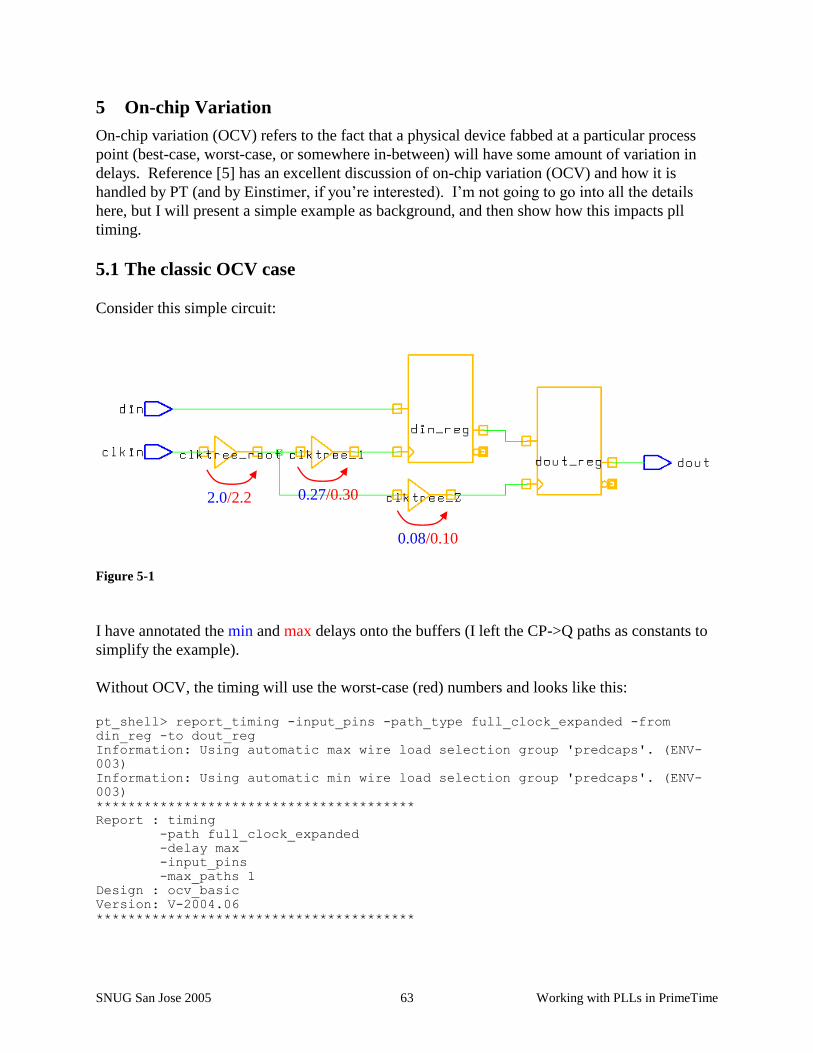
SNUG San Jose 2005 Working with PLLs in PrimeTime 63
5 On-chip Variation
On-chip variation (OCV) refers to the fact that a physical device fabbed at a particular process
point (best-case, worst-case, or somewhere in-between) will have some amount of variation in
delays. Reference [5] has an excellent discussion of on-chip variation (OCV) and how it is
handled by PT (and by Einstimer, if you’re interested). I’m not going to go into all the details
here, but I will present a simple example as background, and then show how this impacts pll
timing.
5.1 The classic OCV case
Consider this simple circuit:
Figure 5-1
I have annotated the min and max delays onto the buffers (I left the CP->Q paths as constants to
simplify the example).
Without OCV, the timing will use the worst-case (red) numbers and looks like this:
pt_shell> report_timing -input_pins -path_type full_clock_expanded -from
din_reg -to dout_reg
Information: Using automatic max wire load selection group 'predcaps'. (ENV-
003)
Information: Using automatic min wire load selection group 'predcaps'. (ENV-
003)
****************************************
Report : timing
-path full_clock_expanded
-delay max
-input_pins
-max_paths 1
Design : ocv_basic
Version: V-2004.06
****************************************
2.0/2.2
0.08/0.10
0.27/0.30

SNUG San Jose 2005 Working with PLLs in PrimeTime 64
Startpoint: din_reg (rising edge-triggered flip-flop clocked by clkin)
Endpoint: dout_reg (rising edge-triggered flip-flop clocked by clkin)
Path Group: clkin
Path Type: max
Point Incr Path
---------------------------------------------------------------
clock clkin (rise edge) 0.00 0.00
clock source latency 0.00 0.00
clkin (in) 0.00 0.00 r
clktree_root/I (bufbd1) 0.00 0.00 r
clktree_root/Z (bufbd1) 2.20 * 2.20 r
clktree_1/I (bufbd1) 0.00 2.20 r
clktree_1/Z (bufbd1) 0.30 * 2.50 r
din_reg/CP (dfnrb1) 0.00 2.50 r
din_reg/Q (dfnrb1) <- 0.32 * 2.82 r
dout_reg/D (dfnrb1) 0.00 2.82 r
data arrival time 2.82
clock clkin (rise edge) 10.00 10.00
clock source latency 0.00 10.00
clkin (in) 0.00 10.00 r
clktree_root/I (bufbd1) 0.00 10.00 r
clktree_root/Z (bufbd1) 2.20 * 12.20 r
clktree_2/I (bufbd1) 0.00 12.20 r
clktree_2/Z (bufbd1) 0.10 * 12.30 r
dout_reg/CP (dfnrb1) 0.00 12.30 r
library setup time -0.08 12.22
data required time 12.22
---------------------------------------------------------------
data required time 12.22
data arrival time -2.82
---------------------------------------------------------------
slack (MET) 9.40
Let’s look at that trace in a little more detail. The timing calculation is like this:
slack = period + capture_clock
- data_arrival
slack = period + Tclktree_root + Tclktree_2 – Tsu
- ( Tclktree_root + Tclktree_1 + Tcp2q)
= 10.0 + 2.20 + 0.10 - 0.08
- ( 2.20 + 0.30 + 0.32)
= 9.40
Now let’s turn on OCV analysis. In this example, I’m using an SDF file with the worst case
values in the 3rd
part of the triplet, and the not-quite-worst-case values in the 1st part of the triplet.
So, I turn on OCV with the following command:
read_sdf \
-analysis_type on_chip_variation \
-min_type sdf_min \
-max_type sdf_max \
ocv.sdf
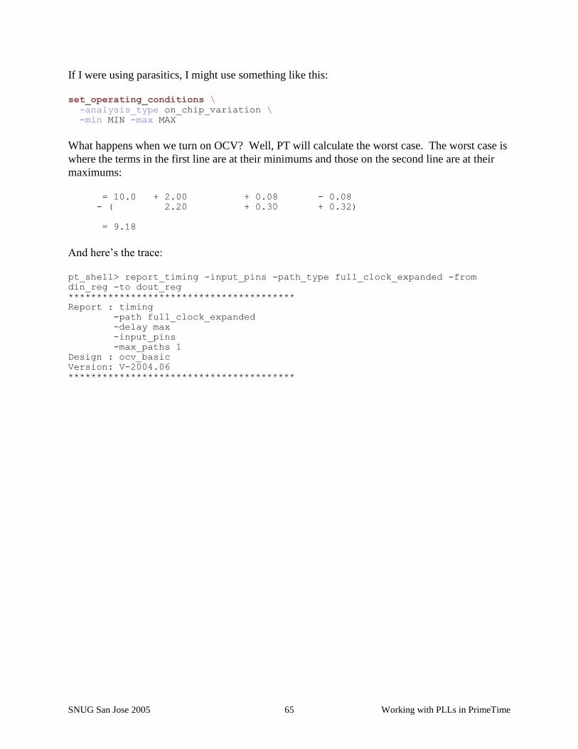
SNUG San Jose 2005 Working with PLLs in PrimeTime 65
If I were using parasitics, I might use something like this:
set_operating_conditions \
-analysis_type on_chip_variation \
-min MIN -max MAX
What happens when we turn on OCV? Well, PT will calculate the worst case. The worst case is
where the terms in the first line are at their minimums and those on the second line are at their
maximums:
= 10.0 + 2.00 + 0.08 - 0.08
- ( 2.20 + 0.30 + 0.32)
= 9.18
And here’s the trace:
pt_shell> report_timing -input_pins -path_type full_clock_expanded -from
din_reg -to dout_reg
****************************************
Report : timing
-path full_clock_expanded
-delay max
-input_pins
-max_paths 1
Design : ocv_basic
Version: V-2004.06
****************************************

SNUG San Jose 2005 Working with PLLs in PrimeTime 66
Startpoint: din_reg (rising edge-triggered flip-flop clocked by clkin)
Endpoint: dout_reg (rising edge-triggered flip-flop clocked by clkin)
Path Group: clkin
Path Type: max
Point Incr Path
---------------------------------------------------------------
clock clkin (rise edge) 0.00 0.00
clock source latency 0.00 0.00
clkin (in) 0.00 0.00 r
clktree_root/I (bufbd1) 0.00 0.00 r
clktree_root/Z (bufbd1) 2.20 * 2.20 r
clktree_1/I (bufbd1) 0.00 2.20 r
clktree_1/Z (bufbd1) 0.30 * 2.50 r
din_reg/CP (dfnrb1) 0.00 2.50 r
din_reg/Q (dfnrb1) <- 0.32 * 2.82 r
dout_reg/D (dfnrb1) 0.00 2.82 r
data arrival time 2.82
clock clkin (rise edge) 10.00 10.00
clock source latency 0.00 10.00
clkin (in) 0.00 10.00 r
clktree_root/I (bufbd1) 0.00 10.00 r
clktree_root/Z (bufbd1) 2.00 * 12.00 r
clktree_2/I (bufbd1) 0.00 12.00 r
clktree_2/Z (bufbd1) 0.08 * 12.08 r
dout_reg/CP (dfnrb1) 0.00 12.08 r
library setup time -0.08 12.00
data required time 12.00
---------------------------------------------------------------
data required time 12.00
data arrival time -2.82
---------------------------------------------------------------
slack (MET) 9.18
5.2 Enter CRPR
But is that really correct? The value for Tclktree_root shows up twice in the calculation. We
have used its min value in one place, and its max value in another. This is not correct. OCV is
not a cycle-to-cycle variation. The clktree_root buffer can be an max or min (or somewhere in
between), but it can’t be at different values on subsequent cycles. Whether we use the min or
max value, the slack will end up being 9.38.
This phenomenon is known as “common path pessimism” or “clock reconvergence pessimism”.
PT can correct this error by examining the clock paths and identifying the common elements.
Instead of using the same value for common elements, it does the simplistic (incorrect)
calculation above, and then adds in a correction factor to the slack. The correction factor (called
“clock reconvergence pessimism”) is the sum of all the differences between min and max for the
common elements.
PT can do this, but you have to turn the feature on:
set timing_remove_clock_reconvergence_pessimism true
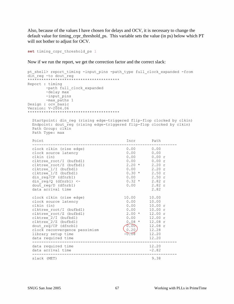
SNUG San Jose 2005 Working with PLLs in PrimeTime 67
Also, because of the values I have chosen for delays and OCV, it is necessary to change the
default value for timing_crpr_threshold_ps. This variable sets the value (in ps) below which PT
will not bother to adjust for OCV.
set timing_crpr_threshold_ps 1
Now if we run the report, we get the correction factor and the correct slack:
pt_shell> report_timing -input_pins -path_type full_clock_expanded -from
din_reg -to dout_reg
****************************************
Report : timing
-path full_clock_expanded
-delay max
-input_pins
-max_paths 1
Design : ocv_basic
Version: V-2004.06
****************************************
Startpoint: din_reg (rising edge-triggered flip-flop clocked by clkin)
Endpoint: dout_reg (rising edge-triggered flip-flop clocked by clkin)
Path Group: clkin
Path Type: max
Point Incr Path
---------------------------------------------------------------
clock clkin (rise edge) 0.00 0.00
clock source latency 0.00 0.00
clkin (in) 0.00 0.00 r
clktree_root/I (bufbd1) 0.00 0.00 r
clktree_root/Z (bufbd1) 2.20 * 2.20 r
clktree_1/I (bufbd1) 0.00 2.20 r
clktree_1/Z (bufbd1) 0.30 * 2.50 r
din_reg/CP (dfnrb1) 0.00 2.50 r
din_reg/Q (dfnrb1) <- 0.32 * 2.82 r
dout_reg/D (dfnrb1) 0.00 2.82 r
data arrival time 2.82
clock clkin (rise edge) 10.00 10.00
clock source latency 0.00 10.00
clkin (in) 0.00 10.00 r
clktree_root/I (bufbd1) 0.00 10.00 r
clktree_root/Z (bufbd1) 2.00 * 12.00 r
clktree_2/I (bufbd1) 0.00 12.00 r
clktree_2/Z (bufbd1) 0.08 * 12.08 r
dout_reg/CP (dfnrb1) 0.00 12.08 r
clock reconvergence pessimism 0.20 12.28
library setup time -0.08 12.20
data required time 12.20
---------------------------------------------------------------
data required time 12.20
data arrival time -2.82
---------------------------------------------------------------
slack (MET) 9.38

SNUG San Jose 2005 Working with PLLs in PrimeTime 68
The “clock reconvergence pessimism” reflects the difference between min and max values for
the shared clock element clktree_root (2.2 – 2.0 = 0.2).
5.3 OCV and PLLs
Now let’s drive this little circuit from a pll:
Figure 5-2
Once again, I have only applied OCV to the clock elements to simplify the example.
Looking at this, we are immediately faced with an issue: how do we assign the source latency to
the pll clock? The delays through the elements in the feedback path have variable delays.
0.08/0.10
0.9/1.0 0.27/0.30 2.0/2.2
0.90/1.00
1.2
2.5

SNUG San Jose 2005 Working with PLLs in PrimeTime 69
The most obvious approach is to calculate a min path and a max path, and apply min and max
source latencies. The min value will be Tref_min – Tfb_max; the max value will be Tref_max –
Tfb_min.
set timing_remove_clock_reconvergence_pessimism true
create_clock -period 10.0 -name clkin [get_ports clkin]
set_propagated_clock clkin
create_clock -period 10.0 -name pllout [get_pins PLL/OUT]
set_propagated_clock pllout
set _path [get_timing_paths -delay max_rise \
-from [get_ports clkin] \
-to [get_pins PLL/CKREF] \
]
set _ref_delay_max [get_attribute $_path arrival]
set _path [get_timing_paths -delay min_rise \
-from [get_ports clkin] \
-to [get_pins PLL/CKREF] \
]
set _ref_delay_min [get_attribute $_path arrival]
set _path [get_timing_paths -delay max_rise \
-from [get_pins PLL/OUT] \
-to [get_pins PLL/FB] \
]
set _fb_delay_max [get_attribute $_path arrival]
set _path [get_timing_paths -delay min_rise \
-from [get_pins PLL/OUT] \
-to [get_pins PLL/FB] \
]
set _fb_delay_min [get_attribute $_path arrival]
set_clock_latency -early -source \
[expr $_ref_delay_min - $_fb_delay_max] \
[get_clocks pllout]
set_clock_latency -late -source \
[expr $_ref_delay_max - $_fb_delay_min] \
[get_clocks pllout]

SNUG San Jose 2005 Working with PLLs in PrimeTime 70
Now look at the clock skew report:
pt_shell> report_clock -skew
****************************************
Report : clock_skew
Design : ocv_pll
Version: V-2004.06
****************************************
Min Condition Source Latency Max Condition Source Latency
--------------------------------------------------------------------------------
Object Early_r Early_f Late_r Late_f Early_r Early_f Late_r Late_f Rel_clk
------------------------------------------------------------------------------------------
pllout -2.40 -2.40 -1.98 -1.98 -2.40 -2.40 -1.98 -1.98
--
Note: set_clock_latency also has –min/-max options. If you use those instead, you get the
following skew report:
pt_shell> report_clock -skew
****************************************
Report : clock_skew
Design : ocv_pll
Version: V-2004.06
****************************************
Min Condition Source Latency Max Condition Source Latency
--------------------------------------------------------------------------------
Object Early_r Early_f Late_r Late_f Early_r Early_f Late_r Late_f Rel_clk
------------------------------------------------------------------------------------------
pllout -2.40 -2.40 -2.40 -2.40 -1.98 -1.98 -1.98 -1.98
--
Since all the timing reports seem to use early/min against late/max, both sets of options have the
same effect (in the reports that I have run). In all the timing traces shown below, it makes no
difference whether you use early/late or min/max. I think that early/late is “more correct” in this
case. I’d be interested to know if there are any timing reports where the distinction matters.
Anyway, the report has two values now.
But does this approach get the correct slack values?

SNUG San Jose 2005 Working with PLLs in PrimeTime 71
Let’s start with the flop-to-flop path. To avoid the chance of using different delays for the same
gate in a single calculation, let’s look at the two extreme cases (Tref@min/Tfb@max and
Tref@max/Tfb@min) separately:
Case 1: Trefclk@min,
Tfb@max
Case2: Trefclk@max, Tfb@min
Tclkinpad 0.9 1.0
Tclktree_root 2.2 2.0
Tclktree_2 0.10 0.08
Tfbdelay 1.0 0.9
Source latency -2.40 -1.98 Figure 5-3
Flop-to-flop setup – Case 1:
slack = period + capture_clock
- data_arrival
slack = period + Tsrclat + Tclktree_root + Tclktree_2 – Tsu
- ( Tsrclat + Tclktree_root + Tclktree_1(max) + Tcp2q)
= 10.0 + -2.40 + 2.2 + 0.10 - 0.08
- ( + -2.40 + 2.2 + 0.30 + 0.32
= 9.4
Flop-to-flop setup – Case 2:
slack = period + Tsrclat + Tclktree_root + Tclktree_2 – Tsu
- ( Tsrclat + Tclktree_root + Tclktree_1(max) + Tcp2q)
= 10.0 + -1.98 + 2.0 + 0.08 - 0.08
- ( + -1.98 + 2.0 + 0.30 + 0.32
= 9.38
So, the minimum slack should be 9.38. What did PT get?
pt_shell> report_timing -input_pins -path_type full_clock_expanded -from
din_reg -to dout_reg
****************************************
Report : timing
-path full_clock_expanded
-delay max
-input_pins
-max_paths 1
Design : ocv_pll
Version: V-2004.06
****************************************

SNUG San Jose 2005 Working with PLLs in PrimeTime 72
Startpoint: din_reg (rising edge-triggered flip-flop clocked by pllout)
Endpoint: dout_reg (rising edge-triggered flip-flop clocked by pllout)
Path Group: pllout
Path Type: max
Point Incr Path
---------------------------------------------------------------
clock pllout (rise edge) 0.00 0.00
clock source latency -1.98 -1.98
PLL/OUT (DUMMYPLL) 0.00 -1.98 r
clktree_root/I (bufbd1) 0.00 -1.98 r
clktree_root/Z (bufbd1) 2.20 * 0.22 r
clktree_1/I (bufbd1) 0.00 0.22 r
clktree_1/Z (bufbd1) 0.30 * 0.52 r
din_reg/CP (dfnrb1) 0.00 0.52 r
din_reg/Q (dfnrb1) <- 0.32 * 0.84 r
dout_reg/D (dfnrb1) 0.00 0.84 r
data arrival time 0.84
clock pllout (rise edge) 10.00 10.00
clock source latency -2.40 7.60
PLL/OUT (DUMMYPLL) 0.00 7.60 r
clktree_root/I (bufbd1) 0.00 7.60 r
clktree_root/Z (bufbd1) 2.00 * 9.60 r
clktree_2/I (bufbd1) 0.00 9.60 r
clktree_2/Z (bufbd1) 0.08 * 9.68 r
dout_reg/CP (dfnrb1) 0.00 9.68 r
clock reconvergence pessimism 0.62 10.30
library setup time -0.08 10.22
data required time 10.22
---------------------------------------------------------------
data required time 10.22
data arrival time -0.84
---------------------------------------------------------------
slack (MET) 9.38
PT got the correct answer, but the trace looks a little strange. In the explicit calculations above, it
is easy to see that the pll source latency will cancel. But PT used the max source latency value
for the data launch, and the min value for the data capture (don’t forget that -1.98 > -2.40 !). Yet
it still got the correct slack. How?
Take a look at the “clock reconvergence pessimism” value. The only common element in the
clock paths of the two flops is clktree_root. The min/max difference on this gate is 0.2. So why
is the clock reconvergence pessimism 0.62? Because PT cleverly recognized that the pll source
latency is also a common path. So it gave back an additional -1.98 – (-2.40) = 0.42 of credit! It
works!

SNUG San Jose 2005 Working with PLLs in PrimeTime 73
The same happens on the hold calculation.
pt_shell> report_timing -input_pins -path_type full_clock_expanded -from
din_reg -to dout_reg -delay min
****************************************
Report : timing
-path full_clock_expanded
-delay min
-input_pins
-max_paths 1
Design : ocv_pll
Version: V-2004.06
****************************************
Startpoint: din_reg (rising edge-triggered flip-flop clocked by pllout)
Endpoint: dout_reg (rising edge-triggered flip-flop clocked by pllout)
Path Group: pllout
Path Type: min
Point Incr Path
---------------------------------------------------------------
clock pllout (rise edge) 0.00 0.00
clock source latency -2.40 -2.40
PLL/OUT (DUMMYPLL) 0.00 -2.40 r
clktree_root/I (bufbd1) 0.00 -2.40 r
clktree_root/Z (bufbd1) 2.00 * -0.40 r
clktree_1/I (bufbd1) 0.00 -0.40 r
clktree_1/Z (bufbd1) 0.27 * -0.13 r
din_reg/CP (dfnrb1) 0.00 -0.13 r
din_reg/Q (dfnrb1) <- 0.32 * 0.19 f
dout_reg/D (dfnrb1) 0.00 0.19 f
data arrival time 0.19
clock pllout (rise edge) 0.00 0.00
clock source latency -1.98 -1.98
PLL/OUT (DUMMYPLL) 0.00 -1.98 r
clktree_root/I (bufbd1) 0.00 -1.98 r
clktree_root/Z (bufbd1) 2.20 * 0.22 r
clktree_2/I (bufbd1) 0.00 0.22 r
clktree_2/Z (bufbd1) 0.10 * 0.32 r
dout_reg/CP (dfnrb1) 0.00 0.32 r
clock reconvergence pessimism -0.62 -0.30
library hold time 0.01 -0.29
data required time -0.29
---------------------------------------------------------------
data required time -0.29
data arrival time -0.19
---------------------------------------------------------------
slack (MET) 0.48

SNUG San Jose 2005 Working with PLLs in PrimeTime 74
5.4 The OCV/PLL excess pessimism problem
So much for the good news. Now let’s look at the i/o timing. We’ll use the same i/o constraints
as before:
set_input_delay -max 8.0 -clock clkin [get_ports din]
set_input_delay -min 0.5 -clock clkin [get_ports din]
set_output_delay -max 2.0 -clock clkin [get_ports dout]
set_output_delay -min [expr -1.0 * 0.5] -clock clkin [get_ports dout]
Let’s start with the setup check from input din:
Din setup – Case 1:
slack = period + capture_clock - Tsu
- data_arrival
slack = period + Tsrclat + Tclktree_root + Tclktree_1(min) – Tsu
- ( Tin + Tinpad )
= 10.0 + -2.40 + 2.2 + 0.27 - 0.08
- ( 8.0 + 1.2 )
= 0.79
Din setup – Case 2:
slack = period + Tsrclat + Tclktree_root + Tclktree_1(min) – Tsu
- ( Tin + Tinpad )
= 10.0 + -1.98 + 2.0 + 0.27 - 0.08
- ( 8.0 + 1.2 )
= 1.01
So, the minimum slack should be 0.79.
What did PT get?
pt_shell> report_timing -input_pins -path_type full_clock_expanded -from din
****************************************
Report : timing
-path full_clock_expanded
-delay max
-input_pins
-max_paths 1
Design : ocv_pll
Version: V-2004.06
****************************************
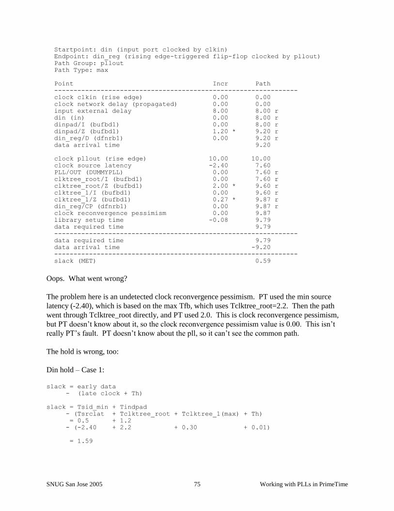
SNUG San Jose 2005 Working with PLLs in PrimeTime 75
Startpoint: din (input port clocked by clkin)
Endpoint: din_reg (rising edge-triggered flip-flop clocked by pllout)
Path Group: pllout
Path Type: max
Point Incr Path
---------------------------------------------------------------
clock clkin (rise edge) 0.00 0.00
clock network delay (propagated) 0.00 0.00
input external delay 8.00 8.00 r
din (in) 0.00 8.00 r
dinpad/I (bufbd1) 0.00 8.00 r
dinpad/Z (bufbd1) 1.20 * 9.20 r
din_reg/D (dfnrb1) 0.00 9.20 r
data arrival time 9.20
clock pllout (rise edge) 10.00 10.00
clock source latency -2.40 7.60
PLL/OUT (DUMMYPLL) 0.00 7.60 r
clktree_root/I (bufbd1) 0.00 7.60 r
clktree_root/Z (bufbd1) 2.00 * 9.60 r
clktree_1/I (bufbd1) 0.00 9.60 r
clktree_1/Z (bufbd1) 0.27 * 9.87 r
din_reg/CP (dfnrb1) 0.00 9.87 r
clock reconvergence pessimism 0.00 9.87
library setup time -0.08 9.79
data required time 9.79
---------------------------------------------------------------
data required time 9.79
data arrival time -9.20
---------------------------------------------------------------
slack (MET) 0.59
Oops. What went wrong?
The problem here is an undetected clock reconvergence pessimism. PT used the min source
latency (-2.40), which is based on the max Tfb, which uses Tclktree_root=2.2. Then the path
went through Tclktree_root directly, and PT used 2.0. This is clock reconvergence pessimism,
but PT doesn’t know about it, so the clock reconvergence pessimism value is 0.00. This isn’t
really PT’s fault. PT doesn’t know about the pll, so it can’t see the common path.
The hold is wrong, too:
Din hold – Case 1:
slack = early data
- (late clock + Th)
slack = Tsid_min + Tindpad
- (Tsrclat + Tclktree_root + Tclktree_1(max) + Th)
= 0.5 + 1.2
- (-2.40 + 2.2 + 0.30 + 0.01)
= 1.59

SNUG San Jose 2005 Working with PLLs in PrimeTime 76
Din hold – Case 2:
slack = Tsid_min + Tindpad
- (Tsrclat + Tclktree_root + Tclktree_1(max) + Th)
= 0.5 + 1.2
- (-1.98 + 2.0 + 0.30 + 0.01)
= 1.37
So, the minimum slack is 1.37. But PT got:
pt_shell> report_timing -input_pins -path_type full_clock_expanded -from din -
delay min
****************************************
Report : timing
-path full_clock_expanded
-delay min
-input_pins
-max_paths 1
Design : ocv_pll
Version: V-2004.06
****************************************
Startpoint: din (input port clocked by clkin)
Endpoint: din_reg (rising edge-triggered flip-flop clocked by pllout)
Path Group: pllout
Path Type: min
Point Incr Path
---------------------------------------------------------------
clock clkin (rise edge) 0.00 0.00
clock network delay (propagated) 0.00 0.00
input external delay 0.50 0.50 f
din (in) 0.00 0.50 f
dinpad/I (bufbd1) 0.00 0.50 f
dinpad/Z (bufbd1) 1.20 * 1.70 f
din_reg/D (dfnrb1) 0.00 1.70 f
data arrival time 1.70
clock pllout (rise edge) 0.00 0.00
clock source latency -1.98 -1.98
PLL/OUT (DUMMYPLL) 0.00 -1.98 r
clktree_root/I (bufbd1) 0.00 -1.98 r
clktree_root/Z (bufbd1) 2.20 * 0.22 r
clktree_1/I (bufbd1) 0.00 0.22 r
clktree_1/Z (bufbd1) 0.30 * 0.52 r
din_reg/CP (dfnrb1) 0.00 0.52 r
clock reconvergence pessimism 0.00 0.52
library hold time 0.01 0.53
data required time 0.53
---------------------------------------------------------------
data required time 0.53
data arrival time -1.70
---------------------------------------------------------------
slack (MET) 1.17

SNUG San Jose 2005 Working with PLLs in PrimeTime 77
So, PT has excess pessimism due to the fact that it doesn’t know about the pll adjustment
explicitly.
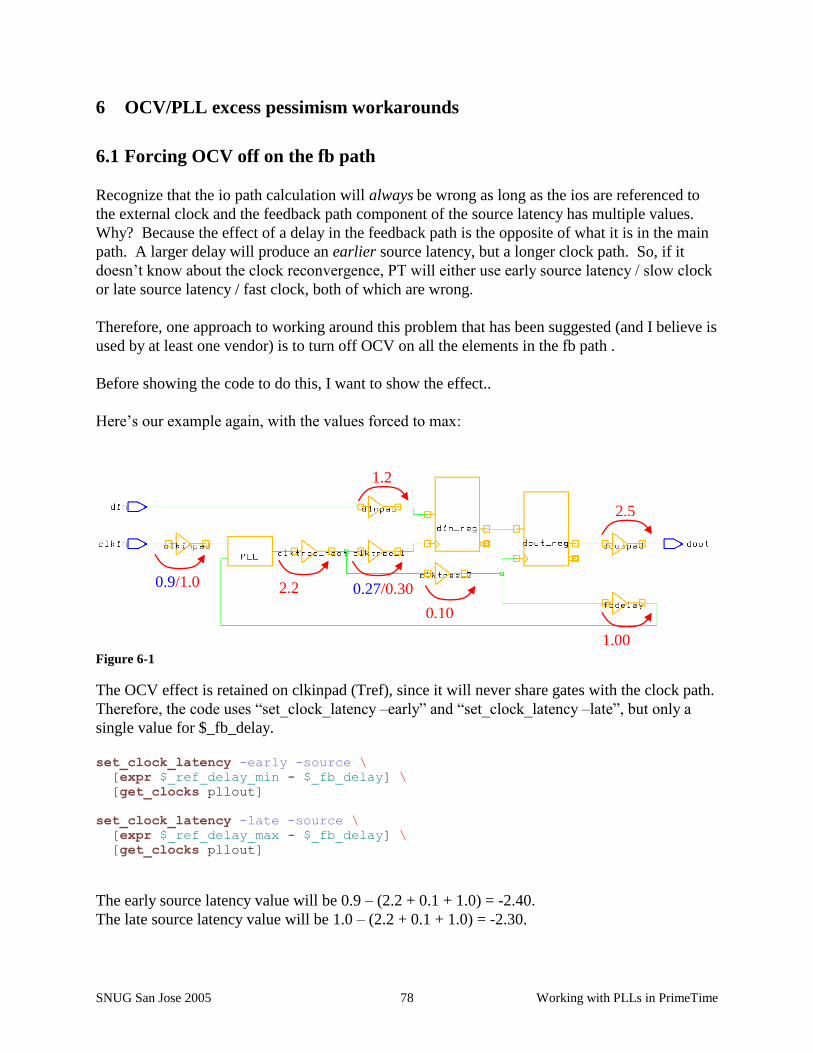
SNUG San Jose 2005 Working with PLLs in PrimeTime 78
6 OCV/PLL excess pessimism workarounds
6.1 Forcing OCV off on the fb path
Recognize that the io path calculation will always be wrong as long as the ios are referenced to
the external clock and the feedback path component of the source latency has multiple values.
Why? Because the effect of a delay in the feedback path is the opposite of what it is in the main
path. A larger delay will produce an earlier source latency, but a longer clock path. So, if it
doesn’t know about the clock reconvergence, PT will either use early source latency / slow clock
or late source latency / fast clock, both of which are wrong.
Therefore, one approach to working around this problem that has been suggested (and I believe is
used by at least one vendor) is to turn off OCV on all the elements in the fb path .
Before showing the code to do this, I want to show the effect..
Here’s our example again, with the values forced to max:
Figure 6-1
The OCV effect is retained on clkinpad (Tref), since it will never share gates with the clock path.
Therefore, the code uses “set_clock_latency –early” and “set_clock_latency –late”, but only a
single value for $_fb_delay.
set_clock_latency -early -source \
[expr $_ref_delay_min - $_fb_delay] \
[get_clocks pllout]
set_clock_latency -late -source \
[expr $_ref_delay_max - $_fb_delay] \
[get_clocks pllout]
The early source latency value will be 0.9 – (2.2 + 0.1 + 1.0) = -2.40.
The late source latency value will be 1.0 – (2.2 + 0.1 + 1.0) = -2.30.
0.10
0.9/1.0 0.27/0.30 2.2
1.00
1.2
2.5

SNUG San Jose 2005 Working with PLLs in PrimeTime 79
OCV is retained on clktree_1 as well, since it is not part of the feedback path.
This approach works fine on the din setup path:
pt_shell> report_timing -input_pins -path_type full_clock_expanded -from din
****************************************
Report : timing
-path full_clock_expanded
-delay max
-input_pins
-max_paths 1
Design : ocv_pll
Version: V-2004.06
****************************************
Startpoint: din (input port clocked by clkin)
Endpoint: din_reg (rising edge-triggered flip-flop clocked by pllout)
Path Group: pllout
Path Type: max
Point Incr Path
---------------------------------------------------------------
clock clkin (rise edge) 0.00 0.00
clock network delay (propagated) 0.00 0.00
input external delay 8.00 8.00 r
din (in) 0.00 8.00 r
dinpad/I (bufbd1) 0.00 8.00 r
dinpad/Z (bufbd1) 1.20 * 9.20 r
din_reg/D (dfnrb1) 0.00 9.20 r
data arrival time 9.20
clock pllout (rise edge) 10.00 10.00
clock source latency -2.40 7.60
PLL/OUT (DUMMYPLL) 0.00 7.60 r
clktree_root/I (bufbd1) 0.00 7.60 r
clktree_root/Z (bufbd1) 2.20 * 9.80 r
clktree_1/I (bufbd1) 0.00 9.80 r
clktree_1/Z (bufbd1) 0.27 * 10.07 r
din_reg/CP (dfnrb1) 0.00 10.07 r
clock reconvergence pessimism 0.00 10.07
library setup time -0.08 9.99
data required time 9.99
---------------------------------------------------------------
data required time 9.99
data arrival time -9.20
---------------------------------------------------------------
slack (MET) 0.79

SNUG San Jose 2005 Working with PLLs in PrimeTime 80
But it doesn’t work on the hold path:
pt_shell> report_timing -input_pins -path_type full_clock_expanded -from din -
delay min
****************************************
Report : timing
-path full_clock_expanded
-delay min
-input_pins
-max_paths 1
Design : ocv_pll
Version: V-2004.06
****************************************
Startpoint: din (input port clocked by clkin)
Endpoint: din_reg (rising edge-triggered flip-flop clocked by pllout)
Path Group: pllout
Path Type: min
Point Incr Path
---------------------------------------------------------------
clock clkin (rise edge) 0.00 0.00
clock network delay (propagated) 0.00 0.00
input external delay 0.50 0.50 f
din (in) 0.00 0.50 f
dinpad/I (bufbd1) 0.00 0.50 f
dinpad/Z (bufbd1) 1.20 * 1.70 f
din_reg/D (dfnrb1) 0.00 1.70 f
data arrival time 1.70
clock pllout (rise edge) 0.00 0.00
clock source latency -2.30 -2.30
PLL/OUT (DUMMYPLL) 0.00 -2.30 r
clktree_root/I (bufbd1) 0.00 -2.30 r
clktree_root/Z (bufbd1) 2.20 * -0.10 r
clktree_1/I (bufbd1) 0.00 -0.10 r
clktree_1/Z (bufbd1) 0.30 * 0.20 r
din_reg/CP (dfnrb1) 0.00 0.20 r
clock reconvergence pessimism 0.00 0.20
library hold time 0.01 0.21
data required time 0.21
---------------------------------------------------------------
data required time 0.21
data arrival time -1.70
---------------------------------------------------------------
slack (MET) 1.49
The correct slack is 1.37. So this approach results in excess optimism.
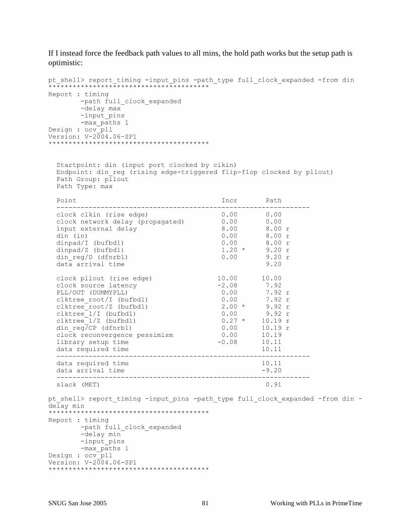
SNUG San Jose 2005 Working with PLLs in PrimeTime 81
If I instead force the feedback path values to all mins, the hold path works but the setup path is
optimistic:
pt_shell> report_timing -input_pins -path_type full_clock_expanded -from din
****************************************
Report : timing
-path full_clock_expanded
-delay max
-input_pins
-max_paths 1
Design : ocv_pll
Version: V-2004.06-SP1
****************************************
Startpoint: din (input port clocked by clkin)
Endpoint: din_reg (rising edge-triggered flip-flop clocked by pllout)
Path Group: pllout
Path Type: max
Point Incr Path
---------------------------------------------------------------
clock clkin (rise edge) 0.00 0.00
clock network delay (propagated) 0.00 0.00
input external delay 8.00 8.00 r
din (in) 0.00 8.00 r
dinpad/I (bufbd1) 0.00 8.00 r
dinpad/Z (bufbd1) 1.20 * 9.20 r
din_reg/D (dfnrb1) 0.00 9.20 r
data arrival time 9.20
clock pllout (rise edge) 10.00 10.00
clock source latency -2.08 7.92
PLL/OUT (DUMMYPLL) 0.00 7.92 r
clktree_root/I (bufbd1) 0.00 7.92 r
clktree_root/Z (bufbd1) 2.00 * 9.92 r
clktree_1/I (bufbd1) 0.00 9.92 r
clktree_1/Z (bufbd1) 0.27 * 10.19 r
din_reg/CP (dfnrb1) 0.00 10.19 r
clock reconvergence pessimism 0.00 10.19
library setup time -0.08 10.11
data required time 10.11
---------------------------------------------------------------
data required time 10.11
data arrival time -9.20
---------------------------------------------------------------
slack (MET) 0.91
pt_shell> report_timing -input_pins -path_type full_clock_expanded -from din -
delay min
****************************************
Report : timing
-path full_clock_expanded
-delay min
-input_pins
-max_paths 1
Design : ocv_pll
Version: V-2004.06-SP1
****************************************

SNUG San Jose 2005 Working with PLLs in PrimeTime 82
Startpoint: din (input port clocked by clkin)
Endpoint: din_reg (rising edge-triggered flip-flop clocked by pllout)
Path Group: pllout
Path Type: min
Point Incr Path
---------------------------------------------------------------
clock clkin (rise edge) 0.00 0.00
clock network delay (propagated) 0.00 0.00
input external delay 0.50 0.50 f
din (in) 0.00 0.50 f
dinpad/I (bufbd1) 0.00 0.50 f
dinpad/Z (bufbd1) 1.20 * 1.70 f
din_reg/D (dfnrb1) 0.00 1.70 f
data arrival time 1.70
clock pllout (rise edge) 0.00 0.00
clock source latency -1.98 -1.98
PLL/OUT (DUMMYPLL) 0.00 -1.98 r
clktree_root/I (bufbd1) 0.00 -1.98 r
clktree_root/Z (bufbd1) 2.00 * 0.02 r
clktree_1/I (bufbd1) 0.00 0.02 r
clktree_1/Z (bufbd1) 0.30 * 0.32 r
din_reg/CP (dfnrb1) 0.00 0.32 r
clock reconvergence pessimism 0.00 0.32
library hold time 0.01 0.33
data required time 0.33
---------------------------------------------------------------
data required time 0.33
data arrival time -1.70
---------------------------------------------------------------
slack (MET) 1.37
The effect is similar for internal paths. Here’s the all-max trace for setup:
pt_shell> report_timing -input_pins -path_type full_clock_expanded -from
din_reg -to dout_reg
****************************************
Report : timing
-path full_clock_expanded
-delay max
-input_pins
-max_paths 1
Design : ocv_pll
Version: V-2004.06
****************************************
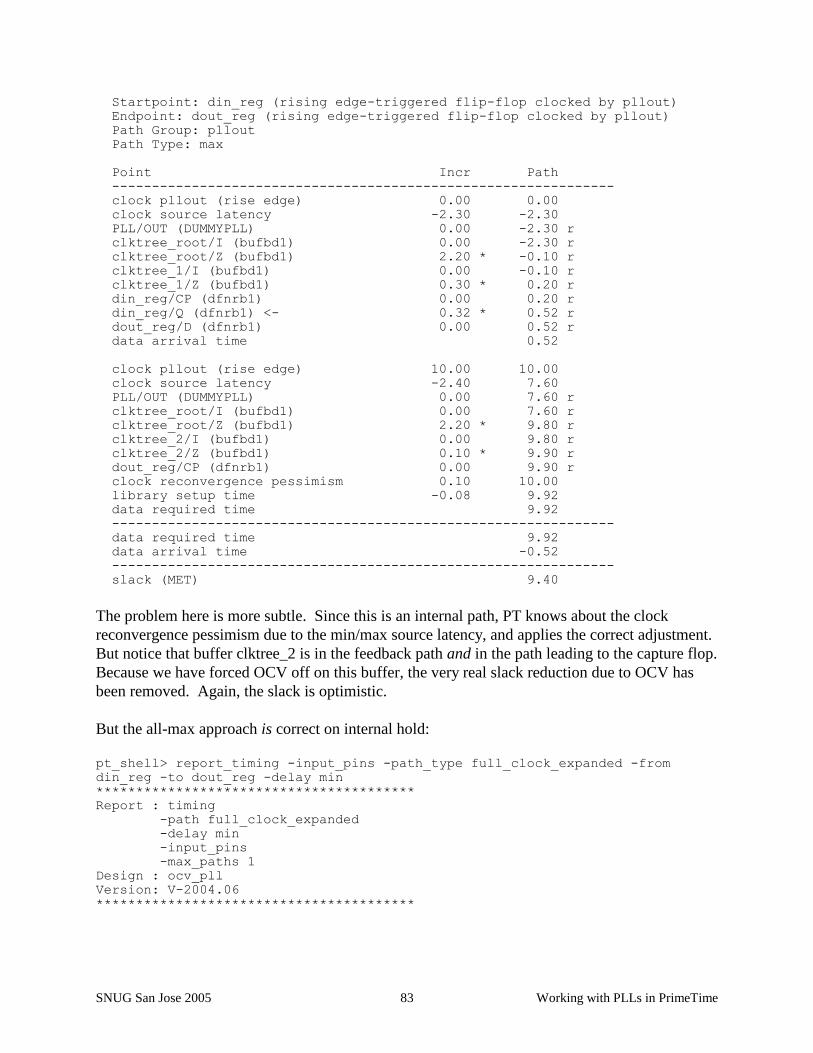
SNUG San Jose 2005 Working with PLLs in PrimeTime 83
Startpoint: din_reg (rising edge-triggered flip-flop clocked by pllout)
Endpoint: dout_reg (rising edge-triggered flip-flop clocked by pllout)
Path Group: pllout
Path Type: max
Point Incr Path
---------------------------------------------------------------
clock pllout (rise edge) 0.00 0.00
clock source latency -2.30 -2.30
PLL/OUT (DUMMYPLL) 0.00 -2.30 r
clktree_root/I (bufbd1) 0.00 -2.30 r
clktree_root/Z (bufbd1) 2.20 * -0.10 r
clktree_1/I (bufbd1) 0.00 -0.10 r
clktree_1/Z (bufbd1) 0.30 * 0.20 r
din_reg/CP (dfnrb1) 0.00 0.20 r
din_reg/Q (dfnrb1) <- 0.32 * 0.52 r
dout_reg/D (dfnrb1) 0.00 0.52 r
data arrival time 0.52
clock pllout (rise edge) 10.00 10.00
clock source latency -2.40 7.60
PLL/OUT (DUMMYPLL) 0.00 7.60 r
clktree_root/I (bufbd1) 0.00 7.60 r
clktree_root/Z (bufbd1) 2.20 * 9.80 r
clktree_2/I (bufbd1) 0.00 9.80 r
clktree_2/Z (bufbd1) 0.10 * 9.90 r
dout_reg/CP (dfnrb1) 0.00 9.90 r
clock reconvergence pessimism 0.10 10.00
library setup time -0.08 9.92
data required time 9.92
---------------------------------------------------------------
data required time 9.92
data arrival time -0.52
---------------------------------------------------------------
slack (MET) 9.40
The problem here is more subtle. Since this is an internal path, PT knows about the clock
reconvergence pessimism due to the min/max source latency, and applies the correct adjustment.
But notice that buffer clktree_2 is in the feedback path and in the path leading to the capture flop.
Because we have forced OCV off on this buffer, the very real slack reduction due to OCV has
been removed. Again, the slack is optimistic.
But the all-max approach is correct on internal hold:
pt_shell> report_timing -input_pins -path_type full_clock_expanded -from
din_reg -to dout_reg -delay min
****************************************
Report : timing
-path full_clock_expanded
-delay min
-input_pins
-max_paths 1
Design : ocv_pll
Version: V-2004.06
****************************************
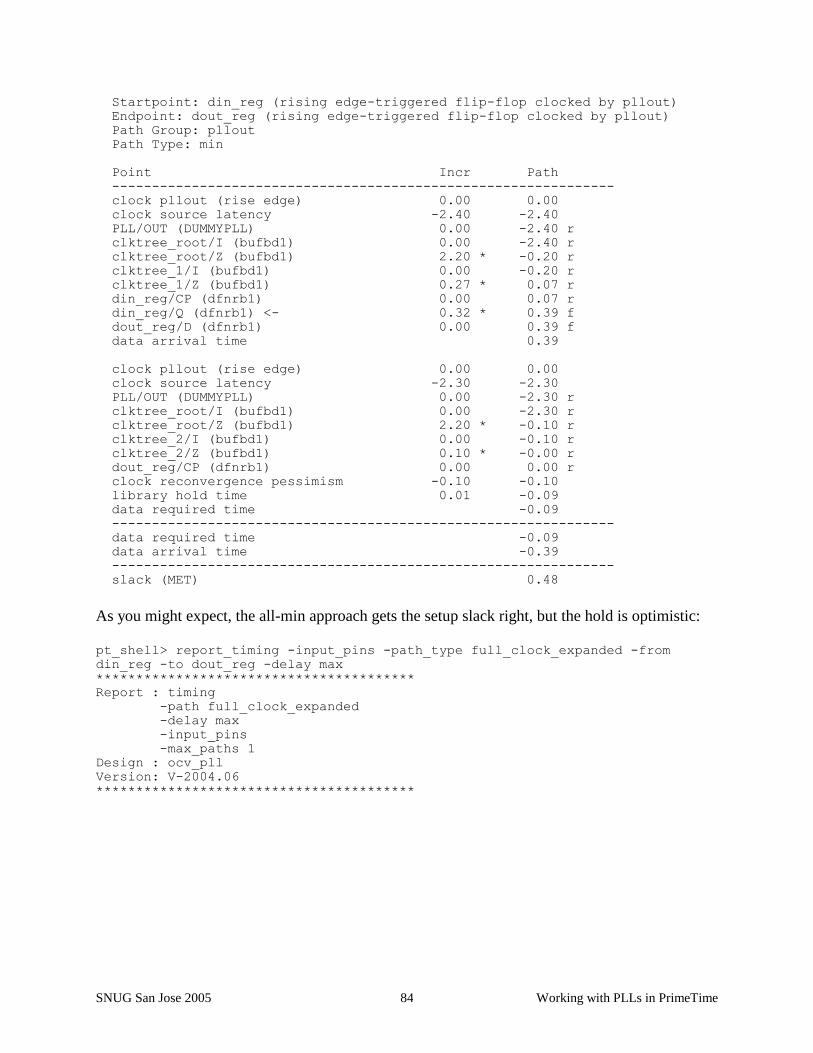
SNUG San Jose 2005 Working with PLLs in PrimeTime 84
Startpoint: din_reg (rising edge-triggered flip-flop clocked by pllout)
Endpoint: dout_reg (rising edge-triggered flip-flop clocked by pllout)
Path Group: pllout
Path Type: min
Point Incr Path
---------------------------------------------------------------
clock pllout (rise edge) 0.00 0.00
clock source latency -2.40 -2.40
PLL/OUT (DUMMYPLL) 0.00 -2.40 r
clktree_root/I (bufbd1) 0.00 -2.40 r
clktree_root/Z (bufbd1) 2.20 * -0.20 r
clktree_1/I (bufbd1) 0.00 -0.20 r
clktree_1/Z (bufbd1) 0.27 * 0.07 r
din_reg/CP (dfnrb1) 0.00 0.07 r
din_reg/Q (dfnrb1) <- 0.32 * 0.39 f
dout_reg/D (dfnrb1) 0.00 0.39 f
data arrival time 0.39
clock pllout (rise edge) 0.00 0.00
clock source latency -2.30 -2.30
PLL/OUT (DUMMYPLL) 0.00 -2.30 r
clktree_root/I (bufbd1) 0.00 -2.30 r
clktree_root/Z (bufbd1) 2.20 * -0.10 r
clktree_2/I (bufbd1) 0.00 -0.10 r
clktree_2/Z (bufbd1) 0.10 * -0.00 r
dout_reg/CP (dfnrb1) 0.00 0.00 r
clock reconvergence pessimism -0.10 -0.10
library hold time 0.01 -0.09
data required time -0.09
---------------------------------------------------------------
data required time -0.09
data arrival time -0.39
---------------------------------------------------------------
slack (MET) 0.48
As you might expect, the all-min approach gets the setup slack right, but the hold is optimistic:
pt_shell> report_timing -input_pins -path_type full_clock_expanded -from
din_reg -to dout_reg -delay max
****************************************
Report : timing
-path full_clock_expanded
-delay max
-input_pins
-max_paths 1
Design : ocv_pll
Version: V-2004.06
****************************************

SNUG San Jose 2005 Working with PLLs in PrimeTime 85
Startpoint: din_reg (rising edge-triggered flip-flop clocked by pllout)
Endpoint: dout_reg (rising edge-triggered flip-flop clocked by pllout)
Path Group: pllout
Path Type: max
Point Incr Path
---------------------------------------------------------------
clock pllout (rise edge) 0.00 0.00
clock source latency -1.98 -1.98
PLL/OUT (DUMMYPLL) 0.00 -1.98 r
clktree_root/I (bufbd1) 0.00 -1.98 r
clktree_root/Z (bufbd1) 2.00 * 0.02 r
clktree_1/I (bufbd1) 0.00 0.02 r
clktree_1/Z (bufbd1) 0.30 * 0.32 r
din_reg/CP (dfnrb1) 0.00 0.32 r
din_reg/Q (dfnrb1) <- 0.32 * 0.64 r
dout_reg/D (dfnrb1) 0.00 0.64 r
data arrival time 0.64
clock pllout (rise edge) 10.00 10.00
clock source latency -2.08 7.92
PLL/OUT (DUMMYPLL) 0.00 7.92 r
clktree_root/I (bufbd1) 0.00 7.92 r
clktree_root/Z (bufbd1) 2.00 * 9.92 r
clktree_2/I (bufbd1) 0.00 9.92 r
clktree_2/Z (bufbd1) 0.08 * 10.00 r
dout_reg/CP (dfnrb1) 0.00 10.00 r
clock reconvergence pessimism 0.10 10.10
library setup time -0.08 10.02
data required time 10.02
---------------------------------------------------------------
data required time 10.02
data arrival time -0.64
---------------------------------------------------------------
slack (MET) 9.38
pt_shell> report_timing -input_pins -path_type full_clock_expanded -from
din_reg -to dout_reg -delay min
****************************************
Report : timing
-path full_clock_expanded
-delay min
-input_pins
-max_paths 1
Design : ocv_pll
Version: V-2004.06
****************************************
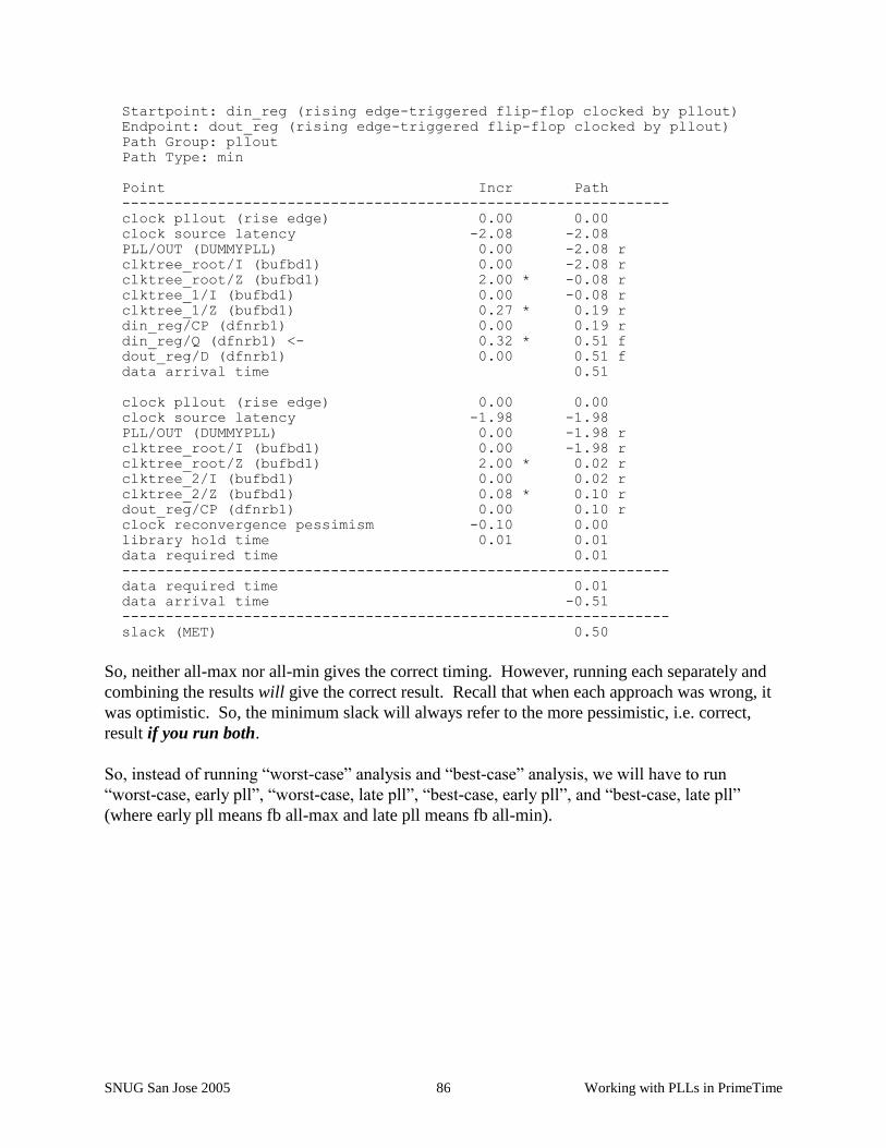
SNUG San Jose 2005 Working with PLLs in PrimeTime 86
Startpoint: din_reg (rising edge-triggered flip-flop clocked by pllout)
Endpoint: dout_reg (rising edge-triggered flip-flop clocked by pllout)
Path Group: pllout
Path Type: min
Point Incr Path
---------------------------------------------------------------
clock pllout (rise edge) 0.00 0.00
clock source latency -2.08 -2.08
PLL/OUT (DUMMYPLL) 0.00 -2.08 r
clktree_root/I (bufbd1) 0.00 -2.08 r
clktree_root/Z (bufbd1) 2.00 * -0.08 r
clktree_1/I (bufbd1) 0.00 -0.08 r
clktree_1/Z (bufbd1) 0.27 * 0.19 r
din_reg/CP (dfnrb1) 0.00 0.19 r
din_reg/Q (dfnrb1) <- 0.32 * 0.51 f
dout_reg/D (dfnrb1) 0.00 0.51 f
data arrival time 0.51
clock pllout (rise edge) 0.00 0.00
clock source latency -1.98 -1.98
PLL/OUT (DUMMYPLL) 0.00 -1.98 r
clktree_root/I (bufbd1) 0.00 -1.98 r
clktree_root/Z (bufbd1) 2.00 * 0.02 r
clktree_2/I (bufbd1) 0.00 0.02 r
clktree_2/Z (bufbd1) 0.08 * 0.10 r
dout_reg/CP (dfnrb1) 0.00 0.10 r
clock reconvergence pessimism -0.10 0.00
library hold time 0.01 0.01
data required time 0.01
---------------------------------------------------------------
data required time 0.01
data arrival time -0.51
---------------------------------------------------------------
slack (MET) 0.50
So, neither all-max nor all-min gives the correct timing. However, running each separately and
combining the results will give the correct result. Recall that when each approach was wrong, it
was optimistic. So, the minimum slack will always refer to the more pessimistic, i.e. correct,
result if you run both.
So, instead of running “worst-case” analysis and “best-case” analysis, we will have to run
“worst-case, early pll”, “worst-case, late pll”, “best-case, early pll”, and “best-case, late pll”
(where early pll means fb all-max and late pll means fb all-min).

SNUG San Jose 2005 Working with PLLs in PrimeTime 87
So, how do we force the all-min and all-max values onto the gates in the fb loop? To illustrate
this better, I’m going to change the example a little bit. Up to now, we have ignored net delays
to simplify the examples. Now I want to include at least one net delay. So that the expected
slack numbers don’t change, I’ll split the delay in the “fbdelay” buffer into 2 components – a cell
delay and a net delay, like this:
Figure 6-2
I’ve done this so that the net delay will be seen more explicitly.
There are a variety of ways to force the delay values along the feedback loop. You could use perl
to modify the SDF and create fb-max and fb-min (early_pll and late_pll) versions. You could
use the tricks shown in reference [4] to perl the output of report_timing to create
set_annotated_delay commands, or even a mini-SDF file. But I think the most straightforward
way is to use get_timing_paths to fetch the desired timing information after the OCV SDF has
been read in and then use set_annotated_delay to force the desired value for min and max.
The basic approach is to do a get_timing_paths on the feedback path, then extract a collection
called “points”, which is an attribute of the path. We can then foreach (foreach_in_collection)
our way through these points, and use the arrival attribute of each point to calculate the
appropriate value for set_annotated delay.
0.08/0.10
0.9/1.0 0.27/0.30 2.0/2.2
0.45/0.50
1.2
2.5
0.45/0.50

SNUG San Jose 2005 Working with PLLs in PrimeTime 88
So, here’s my proc for doing this - &build_cmd_to_fix_delays. It takes one argument – the path
returned from get_timing_paths. It returns a command for setting the annotated delays:
proc &build_cmd_to_fix_delays {_path} {
# init internal variables
set _cmd {}
set _prevpin {}
set _prevarrival 0
# Go through points in path
foreach_in_collection _point [get_attribute $_path points] {
set _object [get_attribute $_point object]
set _pinname [get_object_name $_object]
set _class [get_attribute $_object object_class]
set _arrival [get_attribute $_point arrival]
# If this isn't the first pin
if {$_prevpin != {} } {
# And it *is* a pin (not a port)
if {$_class == "pin"} {
set _pin_direction [get_attribute $_object pin_direction]
# If this is an input, then the path is a net
if {$_pin_direction == "in"} {
set _nextcmd "set_annotated_delay -net "
# If this is an output, then the path is a cell
} elseif {$_pin_direction == "out"} {
set _nextcmd "set_annotated_delay -cell "
} else {
echo "Err" "or - $_pinname not an in or out port - direction is
$_pin_direction"
}
# Calculate incremental delay
set _incr [expr $_arrival - $_prevarrival]
# Finish command
set _nextcmd "$_nextcmd -from $_prevpin -to $_pinname $_incr ;\n"
# Append to list of commands
set _cmd "$_cmd $_nextcmd"
}
}
# Prepare for next
set _prevpin $_pinname
set _prevarrival $_arrival
}
# Return list of commands
return $_cmd
}

SNUG San Jose 2005 Working with PLLs in PrimeTime 89
A few notes on this code:
1) The get_timing_paths command itself (using the –delay option) will determine whether
the min or max values are used in the set_annotated_delay commands.
2) The set_annotated_delay command needs to know whether the delay belongs to a net or a
gate. To determine this, we can look at the pin direction of the point under consideration.
If it is an input, then the previous point must have been an output, and the path is a net. If
it is an output, then the previous point must have been an input, and the path is a “cell”
(gate) path.
3) The check for “$_class == pin” is to handle the case where the timing path starts or ends
on a port. The “net” between the port and the pad pin is a Verilog anomaly –see reference
[1].
4) We don’t really want to do the set_annotated_delay commands as we go, because this
will cause many unnecessary timing updates. Instead, we will build a set of
set_annotated_delay commands in a variable for later processing.
Now we can use this proc in our script.
First, we turn on CRPR and create the clocks as usual:
set timing_remove_clock_reconvergence_pessimism true
create_clock -period 10.0 -name clkin [get_ports clkin]
set_propagated_clock clkin
create_clock -period 10.0 -name pllout [get_pins PLL/OUT]
set_propagated_clock pllout
Now we get the feedback path in the usual way. Notice, however, that the delay_type argument
is now based on a variable “_delay_type”. This would be set to “max_rise” for early_pll and
“min_rise” for late_pll.
set _path [get_timing_paths -delay $_delay_type \
-from [get_pins PLL/OUT] \
-to [get_pins PLL/FB] \
]
Since we specified the delay type with get_timing_paths, it is perfectly safe to use the arrival
value as the Tfb. We will be overriding the delays along this path, but the override values will be
the same as what was used on this path.
set _fb_delay [get_attribute $_path arrival]
Now we can create the set_annotated_delay commands.
set _sadcmds [&build_cmd_to_fix_delays $_path]

SNUG San Jose 2005 Working with PLLs in PrimeTime 90
We put the command string in a variable for later execution. We’ll execute it at the end before
generating reports to avoid an unnecessary timing updates.
Now we fetch the min and max refclk delays:
set _path [get_timing_paths -delay max_rise \
-from [get_ports clkin] \
-to [get_pins PLL/CKREF] \
]
set _ref_delay_max [get_attribute $_path arrival]
set _path [get_timing_paths -delay min_rise \
-from [get_ports clkin] \
-to [get_pins PLL/CKREF] \
]
set _ref_delay_min [get_attribute $_path arrival]
Now we can set the min and max source latencies. But now the min and max come only from
the min and max ref delays; there’s only one feedback delay value.
set_clock_latency -early -source \
[expr $_ref_delay_min - $_fb_delay] \
[get_clocks pllout]
set_clock_latency -late -source \
[expr $_ref_delay_max - $_fb_delay] \
[get_clocks pllout]
We set the i/o constraints as usual:
set_input_delay -max 8.0 -clock clkin [get_ports din]
set_input_delay -min 0.5 -clock clkin [get_ports din]
set_output_delay -max 2.0 -clock clkin [get_ports dout]
set_output_delay -min [expr -1.0 * 0.5] -clock clkin [get_ports dout]
And now we finally execute the set_annotated_delay command string:
eval $_sadcmds
If we run all this with $_delay_type set to “min_rise”, and generate summary reports, we get:
pt_shell> report_timing -path_type summary -max_paths 100 -nworst 1 -delay max
****************************************
Report : timing
-path summary
-delay max
-max_paths 100
Design : ocv_pll
Version: V-2004.06
****************************************

SNUG San Jose 2005 Working with PLLs in PrimeTime 91
Startpoint Endpoint Slack
------------------------------------------------------------------------
dout_reg/CP (dfnrb1) dout (out) 5.08
din (in) din_reg/D (dfnrb1) 0.91
din_reg/CP (dfnrb1) dout_reg/D (dfnrb1) 9.38
1
pt_shell> report_timing -path_type summary -max_paths 100 -nworst 1 -delay min
****************************************
Report : timing
-path summary
-delay min
-max_paths 100
Design : ocv_pll
Version: V-2004.06
****************************************
Startpoint Endpoint Slack
------------------------------------------------------------------------
dout_reg/CP (dfnrb1) dout (out) 2.32
din_reg/CP (dfnrb1) dout_reg/D (dfnrb1) 0.50
din (in) din_reg/D (dfnrb1) 1.37
If we run it with $_delay_type set to “max_rise”, the summary reports look like this:
pt_shell> report_timing -path_type summary -max_paths 100 -nworst 1 -delay max
****************************************
Report : timing
-path summary
-delay max
-max_paths 100
Design : ocv_pll
Version: V-2004.06
****************************************
Startpoint Endpoint Slack
------------------------------------------------------------------------
dout_reg/CP (dfnrb1) dout (out) 5.18
din (in) din_reg/D (dfnrb1) 0.79
din_reg/CP (dfnrb1) dout_reg/D (dfnrb1) 9.40
pt_shell> report_timing -path_type summary -max_paths 100 -nworst 1 -delay min
****************************************
Report : timing
-path summary
-delay min
-max_paths 100
Design : ocv_pll
Version: V-2004.06
****************************************
Startpoint Endpoint Slack
------------------------------------------------------------------------
dout_reg/CP (dfnrb1) dout (out) 2.22
din_reg/CP (dfnrb1) dout_reg/D (dfnrb1) 0.48
din (in) din_reg/D (dfnrb1) 1.49

SNUG San Jose 2005 Working with PLLs in PrimeTime 92
The slack values in red are the correct calculations. The corresponding path in the other run will
be more optimistic and so it will not matter.
Let’s take a look at that _sadcmds variable. With $_delay_type set to “min_rise”, it looks like
this:
pt_shell> echo $_sadcmds
set_annotated_delay -net -from PLL/OUT -to clktree_root/I 0.0 ;
set_annotated_delay -cell -from clktree_root/I -to clktree_root/Z 2.0 ;
set_annotated_delay -net -from clktree_root/Z -to clktree_2/I
4.29999999998e-05 ;
set_annotated_delay -cell -from clktree_2/I -to clktree_2/Z 0.08 ;
set_annotated_delay -net -from clktree_2/Z -to fbdelay/I 0.45 ;
set_annotated_delay -cell -from fbdelay/I -to fbdelay/Z 0.45 ;
set_annotated_delay -net -from fbdelay/Z -to PLL/FB 0.0 ;
You can see it is using min delays (2.0 for the clktree_root, for example). You can also see the
net delay I inserted (0.45) from clktree_2/Z to fbdelay/I.
With $_delay_type set to “max_rise”, it looks like this:
pt_shell> echo $_sadcmds
set_annotated_delay -net -from PLL/OUT -to clktree_root/I 0.0 ;
set_annotated_delay -cell -from clktree_root/I -to clktree_root/Z 2.2 ;
set_annotated_delay -net -from clktree_root/Z -to clktree_2/I
4.29999999998e-05 ;
set_annotated_delay -cell -from clktree_2/I -to clktree_2/Z 0.1 ;
set_annotated_delay -net -from clktree_2/Z -to fbdelay/I 0.5 ;
set_annotated_delay -cell -from fbdelay/I -to fbdelay/Z 0.5 ;
set_annotated_delay -net -from fbdelay/Z -to PLL/FB 0.0 ;
Now it’s using max delays.
So, we can use this code and run “late_pll” and “early_pll” modes to correct for the pll excess
pessimism problem.

SNUG San Jose 2005 Working with PLLs in PrimeTime 93
The code shown above only works for SDF analysis. Since the set_timing_derate command will
derate our set_annotated_delay values, we need to turn off timing derate for the cells and nets
that we are working on. This means adding “set_timing_derate 1.0 [get_cells <cellname>]” and
“set_timing_derate [get_nets <netname>]” to the set_annotated_delay commands. Without
going into detailed proofs, here’s the code that handles parasitics:
proc &build_cmd_to_fix_delays {_path} {
# init internal variables
set _cmd {}
set _prevpin {}
set _prevarrival 0
# Go through points in path
foreach_in_collection _point [get_attribute $_path points] {
set _object [get_attribute $_point object]
set _pinname [get_object_name $_object]
set _class [get_attribute $_object object_class]
set _arrival [get_attribute $_point arrival]
# If this isn't the first pin
if {$_prevpin != {} } {
# And it *is* a pin (not a port)
if {$_class == "pin"} {
set _pin_direction [get_attribute $_object pin_direction]
# If this is an input, then the path is a net
if {$_pin_direction == "in"} {
set _sadcmd "set_annotated_delay -net "
set _netname [get_object_name [all_connected $_object]]
set _deratecmd "set_timing_derate 1.0 \[get_nets $_netname\] ;\n"
# If this is an output, then the path is a cell
} elseif {$_pin_direction == "out"} {
set _sadcmd "set_annotated_delay -cell "
set _cellname [get_object_name [cell_of $_pinname]]
set _deratecmd "set_timing_derate 1.0 \[get_cells $_cellname\] ;\n"
} else {
echo "Err" "or - $_pinname not an in or out port - direction is
$_pin_direction"
}
# Calculate incremental delay
set _incr [expr $_arrival - $_prevarrival]
# Finish command
set _sadcmd "$_sadcmd -from $_prevpin -to $_pinname $_incr ;\n"
# Append to list of commands
set _cmd "$_cmd $_sadcmd $_deratecmd"
}
}
# Prepare for next
set _prevpin $_pinname
set _prevarrival $_arrival
}
# Return list of commands
return $_cmd
}

SNUG San Jose 2005 Working with PLLs in PrimeTime 94
With $_delay_type set to “min_rise”, $_sadcmds looks like this:
set_annotated_delay -net -from PLL/OUT -to clktree_root/I 0.0 ;
set_timing_derate 1.0 [get_nets pllout] ;
set_annotated_delay -cell -from clktree_root/I -to clktree_root/Z 0.076052 ;
set_timing_derate 1.0 [get_cells clktree_root] ;
set_annotated_delay -net -from clktree_root/Z -to clktree_2/I 3.9e-05 ;
set_timing_derate 1.0 [get_nets clktree] ;
set_annotated_delay -cell -from clktree_2/I -to clktree_2/Z 0.093738 ;
set_timing_derate 1.0 [get_cells clktree_2] ;
set_annotated_delay -net -from clktree_2/Z -to fbdelay/I 4e-05 ;
set_timing_derate 1.0 [get_nets clktree2] ;
set_annotated_delay -cell -from fbdelay/I -to fbdelay/Z 0.065468 ;
set_timing_derate 1.0 [get_cells fbdelay] ;
set_annotated_delay -net -from fbdelay/Z -to PLL/FB 0.0 ;
set_timing_derate 1.0 [get_nets pllfb] ;
The actual delays are different (since I didn’t load in my SDF), but the important thing to notice
is the new “set_timing_derate” commands.

SNUG San Jose 2005 Working with PLLs in PrimeTime 95
6.2 Referencing the i/os to the feedback clock
It sure would be nice to find a way to avoid the OCV/PLL excess pessimism problem without
having to double our PT runs for tapeout. After a lot of messing around, I have come up with a
least a partial workaround for this excess pessimism problem , but it is decidedly weird.
Recall that the problem comes in via source latency which contains path information that is
hidden from PT. So, we’re going to have to eliminate the source latency somehow. But if we do
that, how do we get the timing to match between the refclk and the clock tree?
My basic idea is to reference the i/os to the FB pin on the pll. Remember that this has the same
timing as the REF pin on the pll (that’s what all that source latency calculation did), so its timing
is “near” that of the refclk – it is offset by the refclk delay Tref.
Figure 6-3
So, if we adjust the i/o constraint values by Tref (min or max), we should be able to force the i/o
timing to be calculated correctly. But it will be calculated without reference to refclk. As we
shall see, PT will have the feedback loop timing in the calculation twice, just as with internal
paths. So, it will see the clock reconvergence pessimism and apply the correct adjustment!
There won’t be any effect on the internal paths, since the source latency, combined with the
CRPR adjustment, always cancels.
In detail, the steps are these:
1. Don’t apply any source latency to the pll output clock.
2. Create a divide-by 1 generated clock at the FB pin of the pll.
3. Reference input/output delays to this new generated clock, adjusting the value by
Tref_min or Tref_max as required.
The clock here is the same as the clock here, offset by Tref

SNUG San Jose 2005 Working with PLLs in PrimeTime 96
The code looks like this:
create_clock -period 10.0 -name clkin [get_ports clkin]
set_propagated_clock clkin
create_clock -period 10.0 -name pllout [get_pins PLL/OUT]
set_propagated_clock pllout
# Create the gen'd clock on the fb pin
create_generated_clock \
-source [get_pins PLL/OUT] \
-name pll_fb_clk \
-divide_by 1 \
[get_pins PLL/FB]
set_propagated_clock pll_fb_clk
set _path [get_timing_paths -delay max_rise \
-from [get_ports clkin] \
-to [get_pins PLL/CKREF] \
]
set _ref_delay_max [get_attribute $_path arrival]
set _path [get_timing_paths -delay min_rise \
-from [get_ports clkin] \
-to [get_pins PLL/CKREF] \
]
set _ref_delay_min [get_attribute $_path arrival]
Remember that we have to adjust the input/ouput delays using the ref clk delay, as follows:
# Now set input and output delays using pll_fb_clk
set_input_delay -max \
-clock pll_fb_clk \
[expr 8.0 - $_ref_delay_min] \
[get_ports din]
set_input_delay -min \
-clock pll_fb_clk \
[expr 0.5 - $_ref_delay_max] \
[get_ports din]
set_output_delay -max \
-clock pll_fb_clk \
[expr 2.0 + $_ref_delay_max] \
[get_ports dout]
set_output_delay -min \
-clock pll_fb_clk \
[expr (-1.0 * 0.5) + $_ref_delay_min] \
[get_ports dout]
First we’ll run this without any OCV to verify it reproduces the slack results when the pll/ocv
problem is not present.
Here’s what the summary timing reports look like for this circuit using the traditional technique,
without OCV:
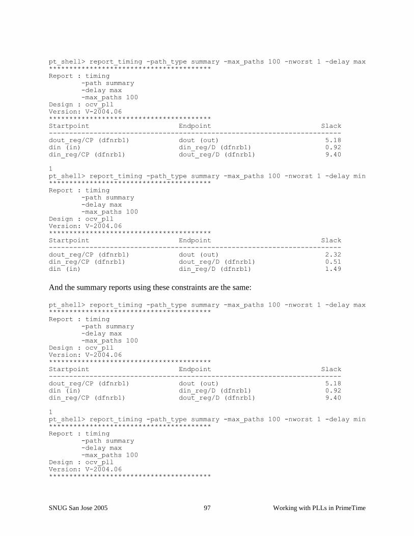
SNUG San Jose 2005 Working with PLLs in PrimeTime 97
pt_shell> report_timing -path_type summary -max_paths 100 -nworst 1 -delay max
****************************************
Report : timing
-path summary
-delay max
-max_paths 100
Design : ocv_pll
Version: V-2004.06
****************************************
Startpoint Endpoint Slack
------------------------------------------------------------------------
dout_reg/CP (dfnrb1) dout (out) 5.18
din (in) din_reg/D (dfnrb1) 0.92
din_reg/CP (dfnrb1) dout_reg/D (dfnrb1) 9.40
1
pt_shell> report_timing -path_type summary -max_paths 100 -nworst 1 -delay min
****************************************
Report : timing
-path summary
-delay max
-max_paths 100
Design : ocv_pll
Version: V-2004.06
****************************************
Startpoint Endpoint Slack
------------------------------------------------------------------------
dout_reg/CP (dfnrb1) dout (out) 2.32
din_reg/CP (dfnrb1) dout_reg/D (dfnrb1) 0.51
din (in) din_reg/D (dfnrb1) 1.49
And the summary reports using these constraints are the same:
pt_shell> report_timing -path_type summary -max_paths 100 -nworst 1 -delay max
****************************************
Report : timing
-path summary
-delay max
-max_paths 100
Design : ocv_pll
Version: V-2004.06
****************************************
Startpoint Endpoint Slack
------------------------------------------------------------------------
dout_reg/CP (dfnrb1) dout (out) 5.18
din (in) din_reg/D (dfnrb1) 0.92
din_reg/CP (dfnrb1) dout_reg/D (dfnrb1) 9.40
1
pt_shell> report_timing -path_type summary -max_paths 100 -nworst 1 -delay min
****************************************
Report : timing
-path summary
-delay max
-max_paths 100
Design : ocv_pll
Version: V-2004.06
****************************************

SNUG San Jose 2005 Working with PLLs in PrimeTime 98
Startpoint Endpoint Slack
------------------------------------------------------------------------
dout_reg/CP (dfnrb1) dout (out) 2.32
din_reg/CP (dfnrb1) dout_reg/D (dfnrb1) 0.51
din (in) din_reg/D (dfnrb1) 1.49
So we didn’t break anything.
Now let’s look at the din path with OCV turned on using the new constraints:
pt_shell> report_timing -input_pins -path_type full_clock_expanded -from din
****************************************
Report : timing
-path full_clock_expanded
-delay max
-input_pins
-max_paths 1
Design : ocv_pll
Version: V-2004.06
****************************************

SNUG San Jose 2005 Working with PLLs in PrimeTime 99
Startpoint: din (input port clocked by pll_fb_clk)
Endpoint: din_reg (rising edge-triggered flip-flop clocked by pllout)
Path Group: pllout
Path Type: max
Point Incr Path
---------------------------------------------------------------
clock pll_fb_clk (rise edge) 0.00 0.00
clock pllout (source latency) 0.00 0.00
PLL/OUT (DUMMYPLL) 0.00 0.00 r
clktree_root/I (bufbd1) 0.00 0.00 r
clktree_root/Z (bufbd1) 2.20 * 2.20 r
clktree_2/I (bufbd1) 0.00 2.20 r
clktree_2/Z (bufbd1) 0.10 * 2.30 r
fbdelay/I (bufbd1) 0.00 2.30 r
fbdelay/Z (bufbd1) 1.00 * 3.30 r
PLL/FB (DUMMYPLL) (gclock source) 0.00 3.30 r
input external delay 7.10 10.40 r
din (in) 0.00 10.40 r
dinpad/I (bufbd1) 0.00 10.40 r
dinpad/Z (bufbd1) 1.20 * 11.60 r
din_reg/D (dfnrb1) 0.00 11.60 r
data arrival time 11.60
clock pllout (rise edge) 10.00 10.00
clock source latency 0.00 10.00
PLL/OUT (DUMMYPLL) 0.00 10.00 r
clktree_root/I (bufbd1) 0.00 10.00 r
clktree_root/Z (bufbd1) 2.00 * 12.00 r
clktree_1/I (bufbd1) 0.00 12.00 r
clktree_1/Z (bufbd1) 0.27 * 12.27 r
din_reg/CP (dfnrb1) 0.00 12.27 r
clock reconvergence pessimism 0.20 12.47
library setup time -0.08 12.39
data required time 12.39
---------------------------------------------------------------
data required time 12.39
data arrival time -11.60
---------------------------------------------------------------
slack (MET) 0.79
Now we get the expected slack value of 0.79. Look carefully at the report. Both paths now go
through the clock tree, so PT recognizes that it used the min delay for clktree_root in one place
and max delay in another and gives us back the lost 0.20 as clock reconvergence pessimism.
How about hold on din?
pt_shell> report_timing -input_pins -path_type full_clock_expanded -from din -
delay min
****************************************
Report : timing
-path full_clock_expanded
-delay min
-input_pins
-max_paths 1
Design : ocv_pll
Version: V-2004.06
****************************************
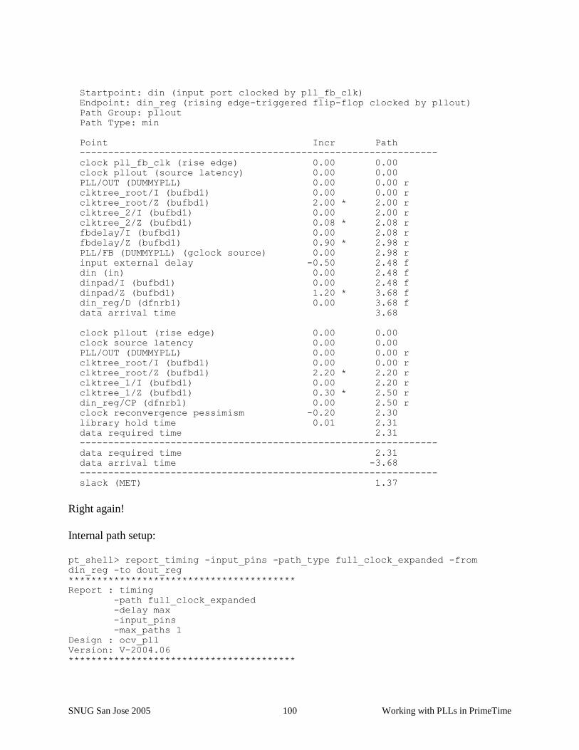
SNUG San Jose 2005 Working with PLLs in PrimeTime 100
Startpoint: din (input port clocked by pll_fb_clk)
Endpoint: din_reg (rising edge-triggered flip-flop clocked by pllout)
Path Group: pllout
Path Type: min
Point Incr Path
---------------------------------------------------------------
clock pll_fb_clk (rise edge) 0.00 0.00
clock pllout (source latency) 0.00 0.00
PLL/OUT (DUMMYPLL) 0.00 0.00 r
clktree_root/I (bufbd1) 0.00 0.00 r
clktree_root/Z (bufbd1) 2.00 * 2.00 r
clktree_2/I (bufbd1) 0.00 2.00 r
clktree_2/Z (bufbd1) 0.08 * 2.08 r
fbdelay/I (bufbd1) 0.00 2.08 r
fbdelay/Z (bufbd1) 0.90 * 2.98 r
PLL/FB (DUMMYPLL) (gclock source) 0.00 2.98 r
input external delay -0.50 2.48 f
din (in) 0.00 2.48 f
dinpad/I (bufbd1) 0.00 2.48 f
dinpad/Z (bufbd1) 1.20 * 3.68 f
din_reg/D (dfnrb1) 0.00 3.68 f
data arrival time 3.68
clock pllout (rise edge) 0.00 0.00
clock source latency 0.00 0.00
PLL/OUT (DUMMYPLL) 0.00 0.00 r
clktree_root/I (bufbd1) 0.00 0.00 r
clktree_root/Z (bufbd1) 2.20 * 2.20 r
clktree_1/I (bufbd1) 0.00 2.20 r
clktree_1/Z (bufbd1) 0.30 * 2.50 r
din_reg/CP (dfnrb1) 0.00 2.50 r
clock reconvergence pessimism -0.20 2.30
library hold time 0.01 2.31
data required time 2.31
---------------------------------------------------------------
data required time 2.31
data arrival time -3.68
---------------------------------------------------------------
slack (MET) 1.37
Right again!
Internal path setup:
pt_shell> report_timing -input_pins -path_type full_clock_expanded -from
din_reg -to dout_reg
****************************************
Report : timing
-path full_clock_expanded
-delay max
-input_pins
-max_paths 1
Design : ocv_pll
Version: V-2004.06
****************************************

SNUG San Jose 2005 Working with PLLs in PrimeTime 101
Startpoint: din_reg (rising edge-triggered flip-flop clocked by pllout)
Endpoint: dout_reg (rising edge-triggered flip-flop clocked by pllout)
Path Group: pllout
Path Type: max
Point Incr Path
---------------------------------------------------------------
clock pllout (rise edge) 0.00 0.00
clock source latency 0.00 0.00
PLL/OUT (DUMMYPLL) 0.00 0.00 r
clktree_root/I (bufbd1) 0.00 0.00 r
clktree_root/Z (bufbd1) 2.20 * 2.20 r
clktree_1/I (bufbd1) 0.00 2.20 r
clktree_1/Z (bufbd1) 0.30 * 2.50 r
din_reg/CP (dfnrb1) 0.00 2.50 r
din_reg/Q (dfnrb1) <- 0.32 * 2.82 r
dout_reg/D (dfnrb1) 0.00 2.82 r
data arrival time 2.82
clock pllout (rise edge) 10.00 10.00
clock source latency 0.00 10.00
PLL/OUT (DUMMYPLL) 0.00 10.00 r
clktree_root/I (bufbd1) 0.00 10.00 r
clktree_root/Z (bufbd1) 2.00 * 12.00 r
clktree_2/I (bufbd1) 0.00 12.00 r
clktree_2/Z (bufbd1) 0.08 * 12.08 r
dout_reg/CP (dfnrb1) 0.00 12.08 r
clock reconvergence pessimism 0.20 12.28
library setup time -0.08 12.20
data required time 12.20
---------------------------------------------------------------
data required time 12.20
data arrival time -2.82
---------------------------------------------------------------
slack (MET) 9.38
This is correct. Note that the slack has been reduced by 0.02 relative to the non-OCV case. This
is the effect of clktree_2 being faster that I pointed out earlier. PT has done it right.
Internal path hold:
pt_shell> report_timing -input_pins -path_type full_clock_expanded -from
din_reg -to dout_reg -delay min
****************************************
Report : timing
-path full_clock_expanded
-delay min
-input_pins
-max_paths 1
Design : ocv_pll
Version: V-2004.06
****************************************
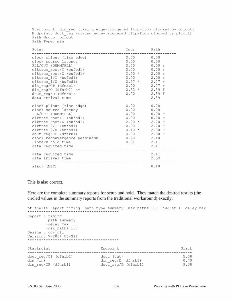
SNUG San Jose 2005 Working with PLLs in PrimeTime 102
Startpoint: din_reg (rising edge-triggered flip-flop clocked by pllout)
Endpoint: dout_reg (rising edge-triggered flip-flop clocked by pllout)
Path Group: pllout
Path Type: min
Point Incr Path
---------------------------------------------------------------
clock pllout (rise edge) 0.00 0.00
clock source latency 0.00 0.00
PLL/OUT (DUMMYPLL) 0.00 0.00 r
clktree_root/I (bufbd1) 0.00 0.00 r
clktree_root/Z (bufbd1) 2.00 * 2.00 r
clktree_1/I (bufbd1) 0.00 2.00 r
clktree_1/Z (bufbd1) 0.27 * 2.27 r
din_reg/CP (dfnrb1) 0.00 2.27 r
din_reg/Q (dfnrb1) <- 0.32 * 2.59 f
dout_reg/D (dfnrb1) 0.00 2.59 f
data arrival time 2.59
clock pllout (rise edge) 0.00 0.00
clock source latency 0.00 0.00
PLL/OUT (DUMMYPLL) 0.00 0.00 r
clktree_root/I (bufbd1) 0.00 0.00 r
clktree_root/Z (bufbd1) 2.20 * 2.20 r
clktree_2/I (bufbd1) 0.00 2.20 r
clktree_2/Z (bufbd1) 0.10 * 2.30 r
dout_reg/CP (dfnrb1) 0.00 2.30 r
clock reconvergence pessimism -0.20 2.10
library hold time 0.01 2.11
data required time 2.11
---------------------------------------------------------------
data required time 2.11
data arrival time -2.59
---------------------------------------------------------------
slack (MET) 0.48
This is also correct.
Here are the complete summary reports for setup and hold. They match the desired results (the
circled values in the summary reports from the traditional workaround) exactly:
pt_shell> report_timing -path_type summary -max_paths 100 -nworst 1 -delay max
****************************************
Report : timing
-path summary
-delay max
-max_paths 100
Design : ocv_pll
Version: V-2004.06-SP1
****************************************
Startpoint Endpoint Slack
------------------------------------------------------------------------
dout_reg/CP (dfnrb1) dout (out) 5.08
din (in) din_reg/D (dfnrb1) 0.79
din_reg/CP (dfnrb1) dout_reg/D (dfnrb1) 9.38
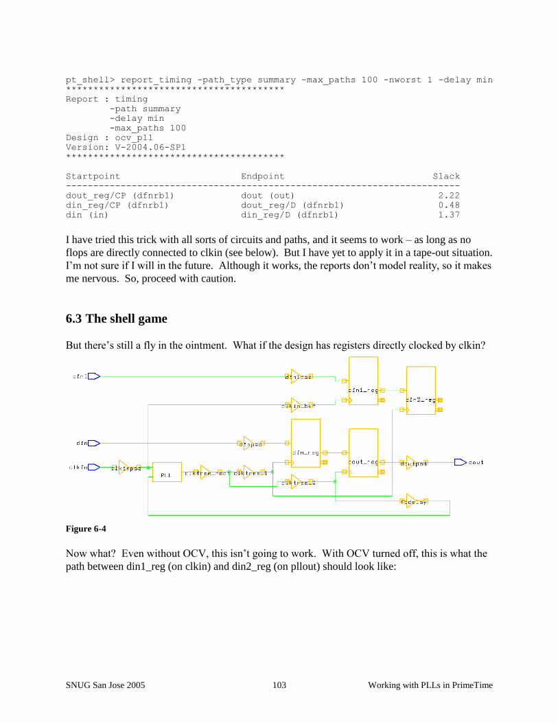
SNUG San Jose 2005 Working with PLLs in PrimeTime 103
pt_shell> report_timing -path_type summary -max_paths 100 -nworst 1 -delay min
****************************************
Report : timing
-path summary
-delay min
-max_paths 100
Design : ocv_pll
Version: V-2004.06-SP1
****************************************
Startpoint Endpoint Slack
------------------------------------------------------------------------
dout_reg/CP (dfnrb1) dout (out) 2.22
din_reg/CP (dfnrb1) dout_reg/D (dfnrb1) 0.48
din (in) din_reg/D (dfnrb1) 1.37
I have tried this trick with all sorts of circuits and paths, and it seems to work – as long as no
flops are directly connected to clkin (see below). But I have yet to apply it in a tape-out situation.
I’m not sure if I will in the future. Although it works, the reports don’t model reality, so it makes
me nervous. So, proceed with caution.
6.3 The shell game
But there’s still a fly in the ointment. What if the design has registers directly clocked by clkin?
Figure 6-4
Now what? Even without OCV, this isn’t going to work. With OCV turned off, this is what the
path between din1_reg (on clkin) and din2_reg (on pllout) should look like:

SNUG San Jose 2005 Working with PLLs in PrimeTime 104
pt_shell> report_timing -input_pins -path_type full_clock_expanded -from
din1_reg -to din2_reg
****************************************
Report : timing
-path full_clock_expanded
-delay max
-input_pins
-max_paths 1
Design : ocv_pll_wclkin
Version: V-2004.06
****************************************
Startpoint: din1_reg (rising edge-triggered flip-flop clocked by clkin)
Endpoint: din2_reg (rising edge-triggered flip-flop clocked by pllout)
Path Group: pllout
Path Type: max
Point Incr Path
---------------------------------------------------------------
clock clkin (rise edge) 0.00 0.00
clock source latency 0.00 0.00
clkin (in) 0.00 0.00 r
clkinpad/I (bufbd1) 0.00 0.00 r
clkinpad/Z (bufbd1) 1.00 * 1.00 r
clkin_buf/I (bufbd1) 0.00 1.00 r
clkin_buf/Z (bufbd1) 0.40 * 1.40 r
din1_reg/CP (dfnrb1) 0.00 1.40 r
din1_reg/Q (dfnrb1) <- 0.32 1.72 r
din2_reg/D (dfnrb1) 0.00 1.72 r
data arrival time 1.72
clock pllout (rise edge) 10.00 10.00
clock source latency -2.30 7.70
PLL/OUT (DUMMYPLL) 0.00 7.70 r
clktree_root/I (bufbd1) 0.00 7.70 r
clktree_root/Z (bufbd1) 2.20 * 9.90 r
clktree_1/I (bufbd1) 0.00 9.90 r
clktree_1/Z (bufbd1) 0.30 * 10.20 r
din2_reg/CP (dfnrb1) 0.00 10.20 r
clock reconvergence pessimism 0.00 10.20
library setup time -0.08 10.12
data required time 10.12
---------------------------------------------------------------
data required time 10.12
data arrival time -1.72
---------------------------------------------------------------
slack (MET) 8.40

SNUG San Jose 2005 Working with PLLs in PrimeTime 105
But this is what it looks like (again, with OCV turned off) using this new technique:
pt_shell> report_timing -input_pins -path_type full_clock_expanded -from
din1_reg -to din2_reg
****************************************
Report : timing
-path full_clock_expanded
-delay max
-input_pins
-max_paths 1
Design : ocv_pll_wclkin
Version: V-2004.06
****************************************
Startpoint: din1_reg (rising edge-triggered flip-flop clocked by clkin)
Endpoint: din2_reg (rising edge-triggered flip-flop clocked by pllout)
Path Group: pllout
Path Type: max
Point Incr Path
---------------------------------------------------------------
clock clkin (rise edge) 0.00 0.00
clock source latency 0.00 0.00
clkin (in) 0.00 0.00 r
clkinpad/I (bufbd1) 0.00 0.00 r
clkinpad/Z (bufbd1) 1.00 * 1.00 r
clkin_buf/I (bufbd1) 0.00 1.00 r
clkin_buf/Z (bufbd1) 0.40 * 1.40 r
din1_reg/CP (dfnrb1) 0.00 1.40 r
din1_reg/Q (dfnrb1) <- 0.32 1.72 r
din2_reg/D (dfnrb1) 0.00 1.72 r
data arrival time 1.72
clock pllout (rise edge) 10.00 10.00
clock source latency 0.00 10.00
PLL/OUT (DUMMYPLL) 0.00 10.00 r
clktree_root/I (bufbd1) 0.00 10.00 r
clktree_root/Z (bufbd1) 2.20 * 12.20 r
clktree_1/I (bufbd1) 0.00 12.20 r
clktree_1/Z (bufbd1) 0.30 * 12.50 r
din2_reg/CP (dfnrb1) 0.00 12.50 r
clock reconvergence pessimism 0.00 12.50
library setup time -0.08 12.42
data required time 12.42
---------------------------------------------------------------
data required time 12.42
data arrival time -1.72
---------------------------------------------------------------
slack (MET) 10.70
The problem is that we are no longer taking the PLL’s time shift into account. The trick of
referencing the i/os to the feedback clock basically moved the operation out in time. If we leave
clkin at time zero, the path from din1_reg to din2_reg (from clkin to the pll clock) will be all
messed up - it will fail to take into account the behavior of the pll.

SNUG San Jose 2005 Working with PLLs in PrimeTime 106
We can fix this by adding the appropriate amount of source latency to clkin:
set_clock_latency -source \
[expr $_fb_delay - $_ref_delay] \
[get_clocks clkin]
Now the path works (without OCV):
pt_shell> report_timing -input_pins -path_type full_clock_expanded -from
din1_reg -to din2_reg
****************************************
Report : timing
-path full_clock_expanded
-delay max
-input_pins
-max_paths 1
Design : ocv_pll_wclkin
Version: V-2004.06
****************************************
Startpoint: din1_reg (rising edge-triggered flip-flop clocked by clkin)
Endpoint: din2_reg (rising edge-triggered flip-flop clocked by pllout)
Path Group: pllout
Path Type: max
Point Incr Path
---------------------------------------------------------------
clock clkin (rise edge) 0.00 0.00
clock source latency 2.30 2.30
clkin (in) 0.00 2.30 r
clkinpad/I (bufbd1) 0.00 2.30 r
clkinpad/Z (bufbd1) 1.00 * 3.30 r
clkin_buf/I (bufbd1) 0.00 3.30 r
clkin_buf/Z (bufbd1) 0.40 * 3.70 r
din1_reg/CP (dfnrb1) 0.00 3.70 r
din1_reg/Q (dfnrb1) <- 0.32 4.02 r
din2_reg/D (dfnrb1) 0.00 4.02 r
data arrival time 4.02
clock pllout (rise edge) 10.00 10.00
clock source latency 0.00 10.00
PLL/OUT (DUMMYPLL) 0.00 10.00 r
clktree_root/I (bufbd1) 0.00 10.00 r
clktree_root/Z (bufbd1) 2.20 * 12.20 r
clktree_1/I (bufbd1) 0.00 12.20 r
clktree_1/Z (bufbd1) 0.30 * 12.50 r
din2_reg/CP (dfnrb1) 0.00 12.50 r
clock reconvergence pessimism 0.00 12.50
library setup time -0.08 12.42
data required time 12.42
---------------------------------------------------------------
data required time 12.42
data arrival time -4.02
---------------------------------------------------------------
slack (MET) 8.40
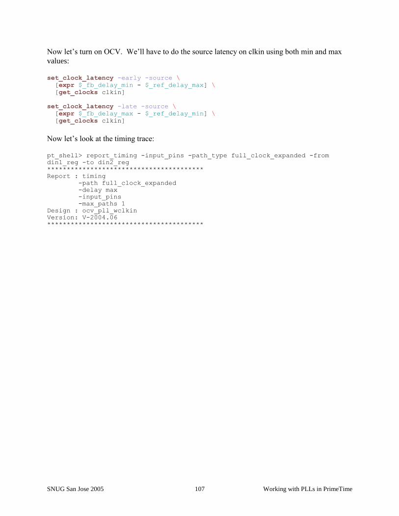
SNUG San Jose 2005 Working with PLLs in PrimeTime 107
Now let’s turn on OCV. We’ll have to do the source latency on clkin using both min and max
values:
set_clock_latency -early -source \
[expr $_fb_delay_min - $_ref_delay_max] \
[get_clocks clkin]
set_clock_latency -late -source \
[expr $_fb_delay_max - $_ref_delay_min] \
[get_clocks clkin]
Now let’s look at the timing trace:
pt_shell> report_timing -input_pins -path_type full_clock_expanded -from
din1_reg -to din2_reg
****************************************
Report : timing
-path full_clock_expanded
-delay max
-input_pins
-max_paths 1
Design : ocv_pll_wclkin
Version: V-2004.06
****************************************
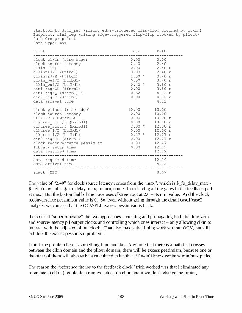
SNUG San Jose 2005 Working with PLLs in PrimeTime 108
Startpoint: din1_reg (rising edge-triggered flip-flop clocked by clkin)
Endpoint: din2_reg (rising edge-triggered flip-flop clocked by pllout)
Path Group: pllout
Path Type: max
Point Incr Path
---------------------------------------------------------------
clock clkin (rise edge) 0.00 0.00
clock source latency 2.40 2.40
clkin (in) 0.00 2.40 r
clkinpad/I (bufbd1) 0.00 2.40 r
clkinpad/Z (bufbd1) 1.00 * 3.40 r
clkin_buf/I (bufbd1) 0.00 3.40 r
clkin_buf/Z (bufbd1) 0.40 * 3.80 r
din1_reg/CP (dfnrb1) 0.00 3.80 r
din1_reg/Q (dfnrb1) <- 0.32 4.12 r
din2_reg/D (dfnrb1) 0.00 4.12 r
data arrival time 4.12
clock pllout (rise edge) 10.00 10.00
clock source latency 0.00 10.00
PLL/OUT (DUMMYPLL) 0.00 10.00 r
clktree_root/I (bufbd1) 0.00 10.00 r
clktree_root/Z (bufbd1) 2.00 * 12.00 r
clktree_1/I (bufbd1) 0.00 12.00 r
clktree_1/Z (bufbd1) 0.27 * 12.27 r
din2_reg/CP (dfnrb1) 0.00 12.27 r
clock reconvergence pessimism 0.00 12.27
library setup time -0.08 12.19
data required time 12.19
---------------------------------------------------------------
data required time 12.19
data arrival time -4.12
---------------------------------------------------------------
slack (MET) 8.07
The value of “2.40” for clock source latency comes from the “max”, which is $_fb_delay_max -
$_ref_delay_min. $_fb_delay_max, in turn, comes from having all the gates in the feedback path
at max. But the bottom half of the trace uses clktree_root at 2.0 – its min value. And the clock
reconvergence pessimism value is 0. So, even without going through the detail case1/case2
analysis, we can see that the OCV/PLL excess pessimism is back.
I also tried “superimposing” the two approaches – creating and propagating both the time-zero
and source-latency pll output clocks and controlling which ones interact – only allowing clkin to
interact with the adjusted pllout clock. That also makes the timing work without OCV, but still
exhibits the excess pessimism problem.
I think the problem here is something fundamental. Any time that there is a path that crosses
between the clkin domain and the pllout domain, there will be excess pessimism, because one or
the other of them will always be a calculated value that PT won’t know contains min/max paths.
The reason the “reference the ios to the feedback clock” trick worked was that I eliminated any
reference to clkin (I could do a remove_clock on clkin and it wouldn’t change the timing

SNUG San Jose 2005 Working with PLLs in PrimeTime 109
reports). Once there are flops directly tied to clkin, there is no way to avoid this domain
crossing.
You can, however, move the problem around. Originally, the excess pessimism appears on the
i/o paths. By referencing the i/os to the feedback clock, and either adding source latency to clkin
or propagating both sets of clocks, you can move the problem to the din1_reg/din2_reg interface
– an internal interface, where there might be more timing slack available.

SNUG San Jose 2005 Working with PLLs in PrimeTime 110
7 Conclusion
Complete and accurate modeling of PLLs is a surprisingly complex task, but a very important
one. There are a lot of issues and effects to consider. Hopefully this paper will provide the
reader with the tools necessary to tackle the project successfully.

SNUG San Jose 2005 Working with PLLs in PrimeTime 111
8 Acknowledgements
The author would like to acknowledge the following people for their assistance and review:
Karthik Rajan for doing a complete, thorough review of the entire paper.
Chris Papademetrious for doing a complete, thorough review of the entire paper.
Matt Weber for lending his expertise in OCV and his insights on jitter, as well as slogging his
way through the entire paper.
Steve Golson for his insights on the issues with PLL models in a parasitics environment, jitter
and for his help in reviewing the entire paper.

SNUG San Jose 2005 Working with PLLs in PrimeTime 112
9 References
(1) Complex Clocking Situations Using PrimeTime
Paul Zimmer
Synopsys Users Group 2000 San Jose
(available at www.zimmerdesignservices.com)
(2) Working with DDRs in PrimeTime
Paul Zimmer, Andrew Cheng
Synopsys Users Group 2001 San Jose
(available at www.zimmerdesignservices.com)
(3) My Favorite DC/PT Shell Tricks
Paul Zimmer
Synopsys Users Group 2002 San Jose
(available at www.zimmerdesignservices.com)
(4) Accounting for PLL Correction in Static Timing Analysis
Solvnet article 000096.html
(5) My Head Hurts, My Timing Stinks, and I Don’t Love On-Chip Variation
Matt Weber – Silicon Logic Engineering
Available from Solvnet
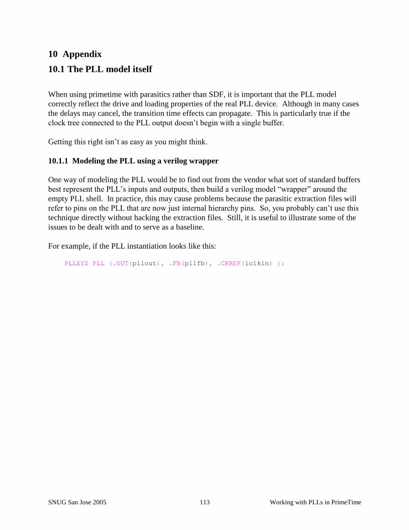
SNUG San Jose 2005 Working with PLLs in PrimeTime 113
10 Appendix
10.1 The PLL model itself
When using primetime with parasitics rather than SDF, it is important that the PLL model
correctly reflect the drive and loading properties of the real PLL device. Although in many cases
the delays may cancel, the transition time effects can propagate. This is particularly true if the
clock tree connected to the PLL output doesn’t begin with a single buffer.
Getting this right isn’t as easy as you might think.
10.1.1 Modeling the PLL using a verilog wrapper
One way of modeling the PLL would be to find out from the vendor what sort of standard buffers
best represent the PLL’s inputs and outputs, then build a verilog model “wrapper” around the
empty PLL shell. In practice, this may cause problems because the parasitic extraction files will
refer to pins on the PLL that are now just internal hierarchy pins. So, you probably can’t use this
technique directly without hacking the extraction files. Still, it is useful to illustrate some of the
issues to be dealt with and to serve as a baseline.
For example, if the PLL instantiation looks like this:
PLLXYZ PLL (.OUT(pllout), .FB(pllfb), .CKREF(iclkin) );

SNUG San Jose 2005 Working with PLLs in PrimeTime 114
I’ll build a 2-stage verilog model that looks like this:
module PLLXYZ (
OUT,
FB,
CKREF
);
output OUT;
input CKREF;
input FB;
DUMMYPLL DUMMYPLL (.DUMMYOUT(pllout), .DUMMYFB(pllfb),
.DUMMYCKREF(pllrefclk) );
bufbd1 fbinbuf(.I(FB), .Z(pllfb));
bufbd1 ckrefinbuf(.I(CKREF), .Z(pllrefclk));
bufbd1 outbuf(.I(pllout), .Z(OUT));
endmodule
module DUMMYPLL (
DUMMYOUT,
DUMMYFB,
DUMMYCKREF
);
output DUMMYOUT;
input DUMMYCKREF;
input DUMMYFB;
endmodule
In this case, I have modeled the PLL’s i/os as standard library buffers (bufbd1’s).
Now for the tricky bit. If I load up the data and report the timing before I have created any
clocks, I get something like this:
pt_shell> set timing_report_unconstrained_paths true
true
pt_shell> report_timing -input_pins -to [get_pins PLL/DUMMYPLL/DUMMYFB]
****************************************
Report : timing
-path full
-delay max
-input_pins
-max_paths 1
Design : idc_pll_example
Version: V-2004.06
****************************************
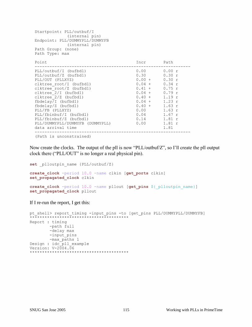
SNUG San Jose 2005 Working with PLLs in PrimeTime 115
Startpoint: PLL/outbuf/I
(internal pin)
Endpoint: PLL/DUMMYPLL/DUMMYFB
(internal pin)
Path Group: (none)
Path Type: max
Point Incr Path
---------------------------------------------------------------
PLL/outbuf/I (bufbd1) 0.00 0.00 r
PLL/outbuf/Z (bufbd1) 0.30 0.30 r
PLL/OUT (PLLXYZ) 0.00 + 0.30 r
clktree_root/I (bufbd1) 0.04 + 0.34 r
clktree_root/Z (bufbd1) 0.41 + 0.75 r
clktree_2/I (bufbd1) 0.04 + 0.79 r
clktree_2/Z (bufbd1) 0.40 + 1.19 r
fbdelay/I (bufbd1) 0.04 + 1.23 r
fbdelay/Z (bufbd1) 0.40 + 1.63 r
PLL/FB (PLLXYZ) 0.00 1.63 r
PLL/fbinbuf/I (bufbd1) 0.04 1.67 r
PLL/fbinbuf/Z (bufbd1) 0.14 1.81 r
PLL/DUMMYPLL/DUMMYFB (DUMMYPLL) 0.00 1.81 r
data arrival time 1.81
---------------------------------------------------------------
(Path is unconstrained)
Now create the clocks. The output of the pll is now “PLL/outbuf/Z”, so I’ll create the pll output
clock there (“PLL/OUT” is no longer a real physical pin).
set _plloutpin_name {PLL/outbuf/Z}
create_clock -period 10.0 -name clkin [get_ports clkin]
set_propagated_clock clkin
create_clock -period 10.0 -name pllout [get_pins ${_plloutpin_name}]
set_propagated_clock pllout
If I re-run the report, I get this:
pt_shell> report_timing -input_pins -to [get_pins PLL/DUMMYPLL/DUMMYFB]
****************************************
Report : timing
-path full
-delay max
-input_pins
-max_paths 1
Design : idc_pll_example
Version: V-2004.06
****************************************
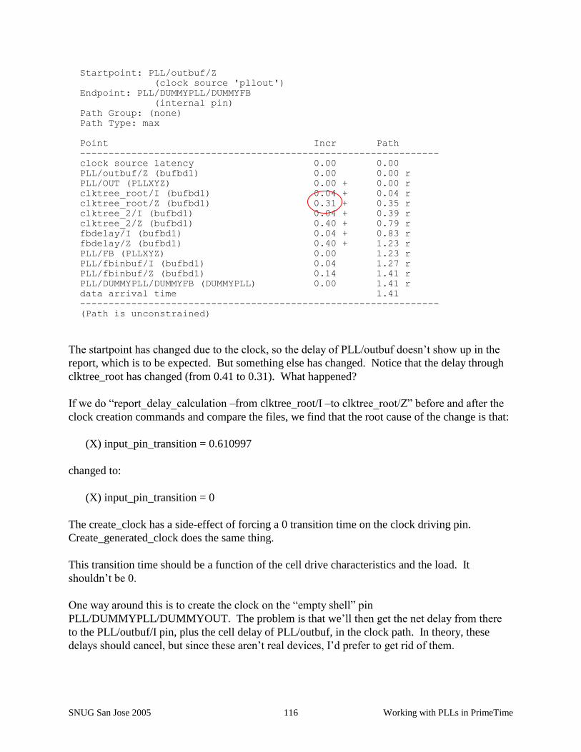
SNUG San Jose 2005 Working with PLLs in PrimeTime 116
Startpoint: PLL/outbuf/Z
(clock source 'pllout')
Endpoint: PLL/DUMMYPLL/DUMMYFB
(internal pin)
Path Group: (none)
Path Type: max
Point Incr Path
---------------------------------------------------------------
clock source latency 0.00 0.00
PLL/outbuf/Z (bufbd1) 0.00 0.00 r
PLL/OUT (PLLXYZ) 0.00 + 0.00 r
clktree_root/I (bufbd1) 0.04 + 0.04 r
clktree_root/Z (bufbd1) 0.31 + 0.35 r
clktree_2/I (bufbd1) 0.04 + 0.39 r
clktree_2/Z (bufbd1) 0.40 + 0.79 r
fbdelay/I (bufbd1) 0.04 + 0.83 r
fbdelay/Z (bufbd1) 0.40 + 1.23 r
PLL/FB (PLLXYZ) 0.00 1.23 r
PLL/fbinbuf/I (bufbd1) 0.04 1.27 r
PLL/fbinbuf/Z (bufbd1) 0.14 1.41 r
PLL/DUMMYPLL/DUMMYFB (DUMMYPLL) 0.00 1.41 r
data arrival time 1.41
---------------------------------------------------------------
(Path is unconstrained)
The startpoint has changed due to the clock, so the delay of PLL/outbuf doesn’t show up in the
report, which is to be expected. But something else has changed. Notice that the delay through
clktree_root has changed (from 0.41 to 0.31). What happened?
If we do “report_delay_calculation –from clktree_root/I –to clktree_root/Z” before and after the
clock creation commands and compare the files, we find that the root cause of the change is that:
(X) input_pin_transition = 0.610997
changed to:
(X) input_pin_transition = 0
The create_clock has a side-effect of forcing a 0 transition time on the clock driving pin.
Create_generated_clock does the same thing.
This transition time should be a function of the cell drive characteristics and the load. It
shouldn’t be 0.
One way around this is to create the clock on the “empty shell” pin
PLL/DUMMYPLL/DUMMYOUT. The problem is that we’ll then get the net delay from there
to the PLL/outbuf/I pin, plus the cell delay of PLL/outbuf, in the clock path. In theory, these
delays should cancel, but since these aren’t real devices, I’d prefer to get rid of them.

SNUG San Jose 2005 Working with PLLs in PrimeTime 117
So, I’ll create the clock on the PLL/outbuf/I pin (which will get rid of the net delay), and use
set_annotated_delay –cell to get rid of the delay through PLL/outbuf:
set _plloutpin_name {PLL/outbuf/I}
set_annotated_delay 0.0 -cell -from PLL/outbuf/I -to PLL/outbuf/Z
create_clock -period 10.0 -name clkin [get_ports clkin]
set_propagated_clock clkin
create_clock -period 10.0 -name pllout [get_pins ${_plloutpin_name}]
set_propagated_clock pllout
Now if we run the reports after the clocks are created, we get the same values as before the
clocks are created:
pt_shell> report_timing -input_pins -to [get_pins PLL/DUMMYPLL/DUMMYFB]
****************************************
Report : timing
-path full
-delay max
-input_pins
-max_paths 1
Design : idc_pll_example
Version: V-2004.06
****************************************
Startpoint: PLL/outbuf/I
(clock source 'pllout')
Endpoint: PLL/DUMMYPLL/DUMMYFB
(internal pin)
Path Group: (none)
Path Type: max
Point Incr Path
---------------------------------------------------------------
clock source latency 0.00 0.00
PLL/outbuf/I (bufbd1) 0.00 0.00 r
PLL/outbuf/Z (bufbd1) 0.00 * 0.00 r
PLL/OUT (PLLXYZ) 0.00 + 0.00 r
clktree_root/I (bufbd1) 0.04 + 0.04 r
clktree_root/Z (bufbd1) 0.41 + 0.45 r
clktree_2/I (bufbd1) 0.04 + 0.49 r
clktree_2/Z (bufbd1) 0.40 + 0.89 r
fbdelay/I (bufbd1) 0.04 + 0.93 r
fbdelay/Z (bufbd1) 0.40 + 1.33 r
PLL/FB (PLLXYZ) 0.00 1.33 r
PLL/fbinbuf/I (bufbd1) 0.04 1.36 r
PLL/fbinbuf/Z (bufbd1) 0.14 1.51 r
PLL/DUMMYPLL/DUMMYFB (DUMMYPLL) 0.00 1.51 r
data arrival time 1.51
---------------------------------------------------------------
(Path is unconstrained)

SNUG San Jose 2005 Working with PLLs in PrimeTime 118
By the way, if you look a the delay calculation on the PLL/outbuf itself, you find that PT used an
input transition time of 0:
pt_shell> report_delay_calculation -from PLL/outbuf/I -to PLL/outbuf/Z
****************************************
Report : delay_calculation
Design : idc_pll_example
Version: V-2004.06
****************************************
From pin: PLL/outbuf/I
To pin: PLL/outbuf/Z
Main Library Units: 1ns 1pF 1kOhm
Library: 'cb13fs120_tsmc_max'
Library Units: 1ns 1pF 1kOhm
Library Cell: 'bufbd1'
arc sense: positive_unate
arc type: cell
Units: 1ns 1pF 1kOhm
Rise Delay
cell delay = 0.301583
Table is indexed by
(X) input_pin_transition = 0
. . .
What we are telling PT is that the PLL output behaves like a bufbd1 with a zero input transition
time. This may or may not be accurate – only your PLL vendor can tell you for sure. But since
this transition time is NOT a function of the load, you can use set_annotated_transition to force
this to the desired value:
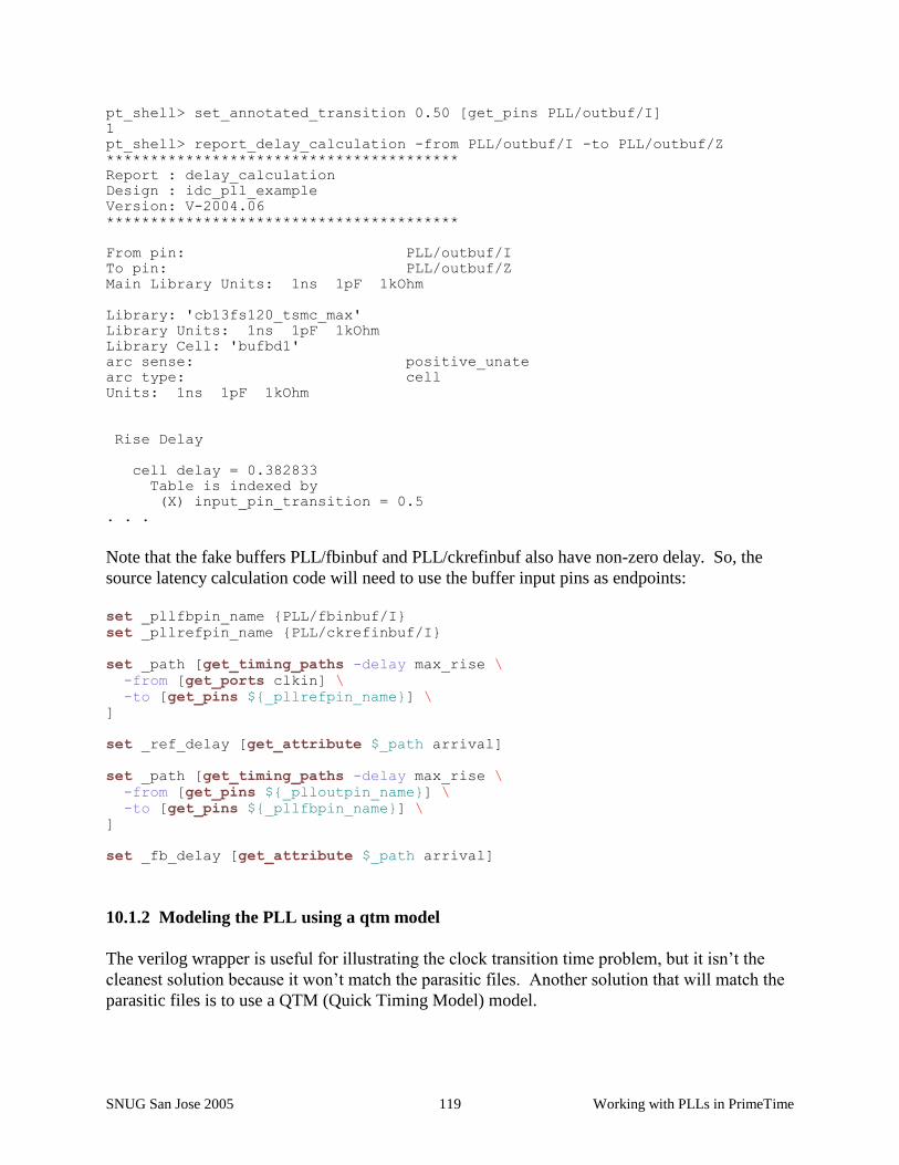
SNUG San Jose 2005 Working with PLLs in PrimeTime 119
pt_shell> set_annotated_transition 0.50 [get_pins PLL/outbuf/I]
1
pt_shell> report_delay_calculation -from PLL/outbuf/I -to PLL/outbuf/Z
****************************************
Report : delay_calculation
Design : idc_pll_example
Version: V-2004.06
****************************************
From pin: PLL/outbuf/I
To pin: PLL/outbuf/Z
Main Library Units: 1ns 1pF 1kOhm
Library: 'cb13fs120_tsmc_max'
Library Units: 1ns 1pF 1kOhm
Library Cell: 'bufbd1'
arc sense: positive_unate
arc type: cell
Units: 1ns 1pF 1kOhm
Rise Delay
cell delay = 0.382833
Table is indexed by
(X) input_pin_transition = 0.5
. . .
Note that the fake buffers PLL/fbinbuf and PLL/ckrefinbuf also have non-zero delay. So, the
source latency calculation code will need to use the buffer input pins as endpoints:
set _pllfbpin_name {PLL/fbinbuf/I}
set _pllrefpin_name {PLL/ckrefinbuf/I}
set _path [get_timing_paths -delay max_rise \
-from [get_ports clkin] \
-to [get_pins ${_pllrefpin_name}] \
]
set _ref_delay [get_attribute $_path arrival]
set _path [get_timing_paths -delay max_rise \
-from [get_pins ${_plloutpin_name}] \
-to [get_pins ${_pllfbpin_name}] \
]
set _fb_delay [get_attribute $_path arrival]
10.1.2 Modeling the PLL using a qtm model
The verilog wrapper is useful for illustrating the clock transition time problem, but it isn’t the
cleanest solution because it won’t match the parasitic files. Another solution that will match the
parasitic files is to use a QTM (Quick Timing Model) model.

SNUG San Jose 2005 Working with PLLs in PrimeTime 120
Using the code in reference [4] as an example, here is the code I used to create a QTM model for
my PLL:
# Make sure library has been read in
if {[sizeof_collection [get_libs -quiet *]] == 0} {
read_db $cell_lib_max
}
set pllname DUMMYPLL
create_qtm_model $pllname
set_qtm_technology -library cb13fs120_tsmc_max
create_qtm_drive_type -lib_cell bufbd1 plldrive
create_qtm_load_type -lib_cell bufbd1 pllckrefload
create_qtm_load_type -lib_cell bufbd1 pllfbload
create_qtm_port {CKREF FB} -type input
set_qtm_port_load -type pllckrefload -factor 1 CKREF
set_qtm_port_load -type pllfbload -factor 1 FB
create_qtm_port {OUT} -type output
set_qtm_port_drive -type plldrive OUT
#create_qtm_delay_arc -from CKREF -to OUT -value 0.0
report_qtm_model
save_qtm_model -library_cell -output ${pllname} -format {db lib}
Notice that I commented out the “create_qtm_delay_arc” line from the example in reference [4].
More on this in the next section. Also, I added code to create drive types and load types and tied
the i/os to these types. I modeled the PLL i/os to be bufbd1’s as in the verilog wrapper example.
When I run this in primetime, it creates two files:
DUMMYPLL_lib.db
DUMMYPLL.lib
The first one is the QTM model. The second one is a .lib description that can be used to create a
technology library model.
To link this in, we do something like this:
set link_path "$link_path DUMMYPLL_lib.db"
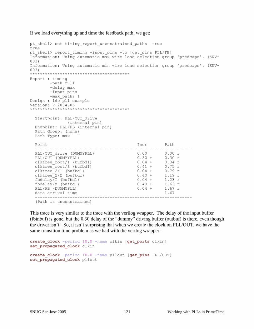
SNUG San Jose 2005 Working with PLLs in PrimeTime 121
If we load everything up and time the feedback path, we get:
pt_shell> set timing_report_unconstrained_paths true
true
pt_shell> report_timing -input_pins -to [get_pins PLL/FB]
Information: Using automatic max wire load selection group 'predcaps'. (ENV-
003)
Information: Using automatic min wire load selection group 'predcaps'. (ENV-
003)
****************************************
Report : timing
-path full
-delay max
-input_pins
-max_paths 1
Design : idc_pll_example
Version: V-2004.06
****************************************
Startpoint: PLL/OUT_drive
(internal pin)
Endpoint: PLL/FB (internal pin)
Path Group: (none)
Path Type: max
Point Incr Path
---------------------------------------------------------------
PLL/OUT_drive (DUMMYPLL) 0.00 0.00 r
PLL/OUT (DUMMYPLL) 0.30 + 0.30 r
clktree_root/I (bufbd1) 0.04 + 0.34 r
clktree_root/Z (bufbd1) 0.41 + 0.75 r
clktree_2/I (bufbd1) 0.04 + 0.79 r
clktree_2/Z (bufbd1) 0.40 + 1.19 r
fbdelay/I (bufbd1) 0.04 + 1.23 r
fbdelay/Z (bufbd1) 0.40 + 1.63 r
PLL/FB (DUMMYPLL) 0.04 + 1.67 r
data arrival time 1.67
---------------------------------------------------------------
(Path is unconstrained)
This trace is very similar to the trace with the verilog wrapper. The delay of the input buffer
(fbinbuf) is gone, but the 0.30 delay of the “dummy” driving buffer (outbuf) is there, even though
the driver isn’t! So, it isn’t surprising that when we create the clock on PLL/OUT, we have the
same transition time problem as we had with the verilog wrapper:
create_clock -period 10.0 -name clkin [get_ports clkin]
set_propagated_clock clkin
create_clock -period 10.0 -name pllout [get_pins PLL/OUT]
set_propagated_clock pllout

SNUG San Jose 2005 Working with PLLs in PrimeTime 122
pt_shell> report_timing -input_pins -to [get_pins PLL/FB]
****************************************
Report : timing
-path full
-delay max
-input_pins
-max_paths 1
Design : idc_pll_example
Version: V-2004.06
****************************************
Startpoint: PLL/OUT (clock source 'pllout')
Endpoint: PLL/FB (internal pin)
Path Group: (none)
Path Type: max
Point Incr Path
---------------------------------------------------------------
clock source latency 0.00 0.00
PLL/OUT (DUMMYPLL) 0.00 0.00 r
clktree_root/I (bufbd1) 0.04 + 0.04 r
clktree_root/Z (bufbd1) 0.31 + 0.35 r
clktree_2/I (bufbd1) 0.04 + 0.39 r
clktree_2/Z (bufbd1) 0.40 + 0.79 r
fbdelay/I (bufbd1) 0.04 + 0.83 r
fbdelay/Z (bufbd1) 0.40 + 1.23 r
PLL/FB (DUMMYPLL) 0.04 + 1.27 r
data arrival time 1.27
---------------------------------------------------------------
(Path is unconstrained)
But now there’s no “outbuf/I” on which to create the clock! Fortunately, there is a funny little
port on the QTM model called “OUT_drive” that is the equivalent of the outbuf/I. So, we’ll
create the clock there:
create_clock -period 10.0 -name clkin [get_ports clkin]
set_propagated_clock clkin
create_clock -period 10.0 -name pllout [get_pins PLL/OUT_drive]
set_propagated_clock pllout
pt_shell> report_timing -input_pins -to [get_pins PLL/FB]
****************************************
Report : timing
-path full
-delay max
-input_pins
-max_paths 1
Design : idc_pll_example
Version: V-2004.06
****************************************

SNUG San Jose 2005 Working with PLLs in PrimeTime 123
Startpoint: PLL/OUT_drive
(clock source 'pllout')
Endpoint: PLL/FB (internal pin)
Path Group: (none)
Path Type: max
Point Incr Path
---------------------------------------------------------------
clock source latency 0.00 0.00
PLL/OUT_drive (DUMMYPLL) 0.00 0.00 r
PLL/OUT (DUMMYPLL) 0.30 + 0.30 r
clktree_root/I (bufbd1) 0.04 + 0.34 r
clktree_root/Z (bufbd1) 0.41 + 0.75 r
clktree_2/I (bufbd1) 0.04 + 0.79 r
clktree_2/Z (bufbd1) 0.40 + 1.19 r
fbdelay/I (bufbd1) 0.04 + 1.23 r
fbdelay/Z (bufbd1) 0.40 + 1.63 r
PLL/FB (DUMMYPLL) 0.04 + 1.67 r
data arrival time 1.67
---------------------------------------------------------------
(Path is unconstrained)
This fixes the transition time problem, but we still have the dummy buffer delay. As before, we
can use set_annotated_delay to zero this value:
pt_shell> set_annotated_delay 0.0 -cell -from PLL/OUT_drive -to PLL/OUT
1
pt_shell> report_timing -input_pins -to [get_pins PLL/FB]
****************************************
Report : timing
-path full
-delay max
-input_pins
-max_paths 1
Design : idc_pll_example
Version: V-2004.06
****************************************
Startpoint: PLL/OUT_drive
(clock source 'pllout')
Endpoint: PLL/FB (internal pin)
Path Group: (none)
Path Type: max
Point Incr Path
---------------------------------------------------------------
clock source latency 0.00 0.00
PLL/OUT_drive (DUMMYPLL) 0.00 0.00 r
PLL/OUT (DUMMYPLL) 0.00 * 0.00 r
clktree_root/I (bufbd1) 0.04 + 0.04 r
clktree_root/Z (bufbd1) 0.41 + 0.45 r
clktree_2/I (bufbd1) 0.04 + 0.49 r
clktree_2/Z (bufbd1) 0.40 + 0.89 r
fbdelay/I (bufbd1) 0.04 + 0.93 r
fbdelay/Z (bufbd1) 0.40 + 1.33 r
PLL/FB (DUMMYPLL) 0.04 + 1.36 r
data arrival time 1.36
---------------------------------------------------------------
(Path is unconstrained)
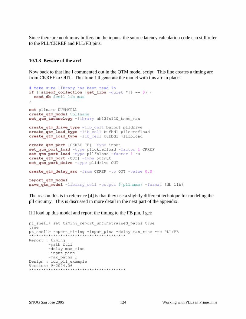
SNUG San Jose 2005 Working with PLLs in PrimeTime 124
Since there are no dummy buffers on the inputs, the source latency calculation code can still refer
to the PLL/CKREF and PLL/FB pins.
10.1.3 Beware of the arc!
Now back to that line I commented out in the QTM model script. This line creates a timing arc
from CKREF to OUT. This time I’ll generate the model with this arc in place:
# Make sure library has been read in
if {[sizeof_collection [get_libs -quiet *]] == 0} {
read_db $cell_lib_max
}
set pllname DUMMYPLL
create_qtm_model $pllname
set_qtm_technology -library cb13fs120_tsmc_max
create_qtm_drive_type -lib_cell bufbd1 plldrive
create_qtm_load_type -lib_cell bufbd1 pllckrefload
create_qtm_load_type -lib_cell bufbd1 pllfbload
create_qtm_port {CKREF FB} -type input
set_qtm_port_load -type pllckrefload -factor 1 CKREF
set_qtm_port_load -type pllfbload -factor 1 FB
create_qtm_port {OUT} -type output
set_qtm_port_drive -type plldrive OUT
create_qtm_delay_arc -from CKREF -to OUT -value 0.0
report_qtm_model
save_qtm_model -library_cell -output ${pllname} -format {db lib}
The reason this is in reference [4] is that they use a slightly different technique for modeling the
pll circuitry. This is discussed in more detail in the next part of the appendix.
If I load up this model and report the timing to the FB pin, I get:
pt_shell> set timing_report_unconstrained_paths true
true
pt_shell> report_timing -input_pins -delay max_rise -to PLL/FB
****************************************
Report : timing
-path full
-delay max_rise
-input_pins
-max_paths 1
Design : idc_pll_example
Version: V-2004.06
****************************************

SNUG San Jose 2005 Working with PLLs in PrimeTime 125
Startpoint: clkin (input port)
Endpoint: PLL/FB (internal pin)
Path Group: (none)
Path Type: max
Point Incr Path
---------------------------------------------------------------
input external delay 0.00 0.00 r
clkin (in) 0.26 + 0.26 r
clkinpad/I (bufbd1) 0.04 + 0.30 r
clkinpad/Z (bufbd1) 0.70 + 1.00 r
PLL/CKREF (DUMMYPLL) 0.10 + 1.10 r
PLL/OUT_drive (DUMMYPLL) 0.00 1.10 r
PLL/OUT (DUMMYPLL) 0.47 + 1.56 r
clktree_root/I (bufbd1) 0.04 + 1.60 r
clktree_root/Z (bufbd1) 0.41 + 2.01 r
clktree_2/I (bufbd1) 0.04 + 2.05 r
clktree_2/Z (bufbd1) 0.40 + 2.45 r
fbdelay/I (bufbd1) 0.04 + 2.49 r
fbdelay/Z (bufbd1) 0.40 + 2.89 r
PLL/FB (DUMMYPLL) 0.04 + 2.93 r
data arrival time 2.93
---------------------------------------------------------------
(Path is unconstrained)
Notice that the path now starts at the clkin input port and runs through the PLL. That’s fine, but
notice also that the delay on the “OUT_drive” to “OUT” path is now 0.47. Let’s look at the
delay calculation for this path:
pt_shell> report_delay_calculation -from PLL/OUT_drive -to PLL/OUT
****************************************
Report : delay_calculation
Design : idc_pll_example
Version: V-2004.06
****************************************
From pin: PLL/OUT_drive
To pin: PLL/OUT
Main Library Units: 1ns 1pF 1kOhm
Library: 'DUMMYPLL_lib'
Library Units: 1ns 1pF 1kOhm
Library Cell: 'DUMMYPLL'
arc sense: positive_unate
arc type: cell
Units: 1ns 1pF 1kOhm
Rise Delay
cell delay = 0.466338
Table is indexed by
(X) input_pin_transition = 1.4439
(Y) output_net_total_cap = 0.07875
. . .

SNUG San Jose 2005 Working with PLLs in PrimeTime 126
This transition time comes from the CKREF pin.
pt_shell> report_timing -input_pins -delay max_rise -to PLL/FB -
transition_time
****************************************
Report : timing
-path full
-delay max_rise
-input_pins
-max_paths 1
-transition_time
Design : idc_pll_example
Version: V-2004.06
****************************************
Startpoint: clkin (input port)
Endpoint: PLL/FB (internal pin)
Path Group: (none)
Path Type: max
Point Trans Incr Path
----------------------------------------------------------------------------
-
input external delay 0.00 0.00 r
clkin (in) 0.26 0.26 + 0.26 r
clkinpad/I (bufbd1) 0.26 0.04 + 0.30 r
clkinpad/Z (bufbd1) 1.44 0.70 + 1.00 r
PLL/CKREF (DUMMYPLL) 1.44 0.10 + 1.10 r
PLL/OUT_drive (DUMMYPLL) 1.44 0.00 1.10 r
PLL/OUT (DUMMYPLL) 0.62 0.47 + 1.56 r
clktree_root/I (bufbd1) 0.62 0.04 + 1.60 r
clktree_root/Z (bufbd1) 0.64 0.41 + 2.01 r
clktree_2/I (bufbd1) 0.64 0.04 + 2.05 r
clktree_2/Z (bufbd1) 0.61 0.40 + 2.45 r
fbdelay/I (bufbd1) 0.61 0.04 + 2.49 r
fbdelay/Z (bufbd1) 0.61 0.40 + 2.89 r
PLL/FB (DUMMYPLL) 0.61 0.04 + 2.93 r
data arrival time 2.93
----------------------------------------------------------------------------
-
(Path is unconstrained)
But this is not correct! The PLL output drive should be independent of the CKREF input
transition time.

SNUG San Jose 2005 Working with PLLs in PrimeTime 127
If we break this arc, we get back to the expected timing:
pt_shell> report_timing -input_pins -delay max_rise -to PLL/FB -
transition_time
****************************************
Report : timing
-path full
-delay max_rise
-input_pins
-max_paths 1
-transition_time
Design : idc_pll_example
Version: V-2004.06
****************************************
Startpoint: PLL/OUT_drive
(internal pin)
Endpoint: PLL/FB (internal pin)
Path Group: (none)
Path Type: max
Point Trans Incr Path
----------------------------------------------------------------------------
-
PLL/OUT_drive (DUMMYPLL) 0.00 0.00 0.00 r
PLL/OUT (DUMMYPLL) 0.61 0.30 + 0.30 r
clktree_root/I (bufbd1) 0.61 0.04 + 0.34 r
clktree_root/Z (bufbd1) 0.64 0.41 + 0.75 r
clktree_2/I (bufbd1) 0.64 0.04 + 0.79 r
clktree_2/Z (bufbd1) 0.61 0.40 + 1.19 r
fbdelay/I (bufbd1) 0.61 0.04 + 1.23 r
fbdelay/Z (bufbd1) 0.61 0.40 + 1.63 r
PLL/FB (DUMMYPLL) 0.61 0.04 + 1.67 r
data arrival time 1.67
----------------------------------------------------------------------------
-
(Path is unconstrained)
It might be possible to fix this by forcing transition times, but since I haven’t found any
advantage in timing through this arc, I’d rather just not have the arc (disable it using
set_disable_timing if the vendor-supplied model has it).
Note that there’s one case where the arc is desirable. If the PLL has a bypass mode for test, then
you need this arc to accurately time test mode. Ideally, the model will make this arc conditional
on the bypass mode pin(s). But if the vendor hasn’t done that, you will need to disable it using
set_disable_timing when you run functional mode STA.
SNUG San Jose 2005 Working with PLLs in PrimeTime 128
10.1.4 Vendor-supplied PLL models
It should be evident from the examples above that the details of the PLL model can be tricky to
get right. If your vendor provides a model of the PLL, make sure you know what’s inside. I got
one once that was like the verilog wrapper (instantiated buffers), but the buffers inputs were tied
low! This caused bizarre behavior in Primetime.
If you’re using parasitics, be sure to use “report_delay_calculation” and examine the output
carefully to make sure the model is doing the right thing. There should not be any edge-rate
dependency of the OUT pin on the REF or FB pins (unless the vendor is sure this is real).
Or get rid of the vendor model and use the QTM method shown above.
10.2 Why I do it my way
Many people use the approach described in the Synopsys App Note (Reference [4]). This paper
wouldn’t be complete if I didn’t explain why I do it differently.
Leaving aside the minor detail of how the source latency is extracted, the Synopsys App Note
uses a fundamentally different approach than the one I have described in this paper. They create
a dummy model with a timing arc from the REF pin to the pll OUT pin. They then apply the
source latency as an annotated delay on this arc. The result is that there is only one clock – the
reference clock, which propagates through the pll with negative delay.
I see several problems with this approach:
1. Duty cycle will be inherited from the ref clock instead of being independent.
2. I don’t see how you can model jitter correctly with only one clock.
3. The annotated delay will get scaled by OCV.
4. It creates a link between the input transition time at the ref pin of the PLL and the output
driver of the PLL, which isn’t correct.
Although there may be solutions to these problems (I’ve never used this approach, so I’ve never
tried to find any), I think they all stem from a fundamental problem – this approach doesn’t
model reality. A real pll does not simply forward the ref clock with a negative delay, it creates a
whole new clock on its output pin. The characteristics of this clock depend on phase and
frequency information from the REF and FB inputs, but the fact remains that it is a new clock.
That’s why my approach creates a new clock on the pll OUT pin.

SNUG San Jose 2005 Working with PLLs in PrimeTime 129
10.3 Modeling duty cycle using set_clock_latency early/late
The “set_clock_latency” command can be used to model clock duty cycle, but only by making
use of features intended for other uses.
Here is our example circuit again:
Notice that set_clock_latency has both –early/-late and –min/-max options:
pt_shell> help -v set_clock_latency
set_clock_latency # Capture actual or predicted clock latency
[-rise] (Specify clock rise latency)
[-fall] (Specify clock fall latency)
[-min] (Specify clock rise and fall min condition latency)
[-max] (Specify clock rise and fall max condition latency)
[-source] (Specify clock rise and fall source latency)
[-late] (Specify clock rise and fall late source latency)
[-early] (Specify clock rise and fall early source latency)
delay (Clock latency)
object_list (List of clocks, ports or pins)
The –early/-late set corresponds to early and late arrival. The –min/-max set corresponds to early
and late arrival in “min-max” analysis mode. Either can be tricked into doing the duty cycle
calculation.
We’ll start with –early/-late. If we just try this out-of-the-box, it doesn’t work.
set _period 10.0
set _duty_cycle_min 0.40
set _duty_cycle_max [expr 1.0 - $_duty_cycle_min]
create_clock -period $_period -name clk \
[get_ports clk]
set_propagated_clock clk
set_clock_latency -source -fall -early \
[expr ($_duty_cycle_min - 0.5) * $_period] \
[get_clocks clk]
set_clock_latency -source -fall -late \
[expr ($_duty_cycle_max - 0.5) * $_period] \
[get_clocks clk]
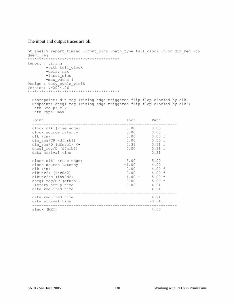
SNUG San Jose 2005 Working with PLLs in PrimeTime 130
The input and output traces are ok:
pt_shell> report_timing -input_pins -path_type full_clock -from din_reg -to
dneg1_reg
****************************************
Report : timing
-path full_clock
-delay max
-input_pins
-max_paths 1
Design : duty_cycle_piclk
Version: V-2004.06
****************************************
Startpoint: din_reg (rising edge-triggered flip-flop clocked by clk)
Endpoint: dneg1_reg (rising edge-triggered flip-flop clocked by clk')
Path Group: clk
Path Type: max
Point Incr Path
---------------------------------------------------------------
clock clk (rise edge) 0.00 0.00
clock source latency 0.00 0.00
clk (in) 0.00 0.00 r
din_reg/CP (dfnrb1) 0.00 0.00 r
din_reg/Q (dfnrb1) <- 0.31 0.31 r
dneg1_reg/D (dfnrb1) 0.00 0.31 r
data arrival time 0.31
clock clk' (rise edge) 5.00 5.00
clock source latency -1.00 4.00
clk (in) 0.00 4.00 f
clkinv/I (inv0d2) 0.00 4.00 f
clkinv/ZN (inv0d2) 1.00 * 5.00 r
dneg1_reg/CP (dfnrb1) 0.00 5.00 r
library setup time -0.09 4.91
data required time 4.91
---------------------------------------------------------------
data required time 4.91
data arrival time -0.31
---------------------------------------------------------------
slack (MET) 4.60

SNUG San Jose 2005 Working with PLLs in PrimeTime 131
pt_shell> report_timing -input_pins -path_type full_clock -from dneg2_reg -to
dout_reg
****************************************
Report : timing
-path full_clock
-delay max
-input_pins
-max_paths 1
Design : duty_cycle_piclk
Version: V-2004.06
****************************************
Startpoint: dneg2_reg (rising edge-triggered flip-flop clocked by clk')
Endpoint: dout_reg (rising edge-triggered flip-flop clocked by clk)
Path Group: clk
Path Type: max
Point Incr Path
---------------------------------------------------------------
clock clk' (rise edge) 5.00 5.00
clock source latency 1.00 6.00
clk (in) 0.00 6.00 f
clkinv/I (inv0d2) 0.00 6.00 f
clkinv/ZN (inv0d2) 1.00 * 7.00 r
dneg2_reg/CP (dfnrb1) 0.00 7.00 r
dneg2_reg/Q (dfnrb1) <- 0.32 7.32 r
dout_reg/D (dfnrb1) 0.00 7.32 r
data arrival time 7.32
clock clk (rise edge) 10.00 10.00
clock source latency 0.00 10.00
clk (in) 0.00 10.00 r
dout_reg/CP (dfnrb1) 0.00 10.00 r
library setup time -0.10 9.90
data required time 9.90
---------------------------------------------------------------
data required time 9.90
data arrival time -7.32
---------------------------------------------------------------
slack (MET) 2.59
But the falling-edge to falling-edge trace is not:
pt_shell> report_timing -input_pins -path_type full_clock -from dneg1_reg -to
dneg2_reg
****************************************
Report : timing
-path full_clock
-delay max
-input_pins
-max_paths 1
Design : duty_cycle_piclk
Version: V-2004.06
****************************************

SNUG San Jose 2005 Working with PLLs in PrimeTime 132
Startpoint: dneg1_reg (rising edge-triggered flip-flop clocked by clk')
Endpoint: dneg2_reg (rising edge-triggered flip-flop clocked by clk')
Path Group: clk
Path Type: max
Point Incr Path
---------------------------------------------------------------
clock clk' (rise edge) 5.00 5.00
clock source latency 1.00 6.00
clk (in) 0.00 6.00 f
clkinv/I (inv0d2) 0.00 6.00 f
clkinv/ZN (inv0d2) 1.00 * 7.00 r
dneg1_reg/CP (dfnrb1) 0.00 7.00 r
dneg1_reg/Q (dfnrb1) <- 0.32 7.32 r
dneg2_reg/D (dfnrb1) 0.00 7.32 r
data arrival time 7.32
clock clk' (rise edge) 15.00 15.00
clock source latency -1.00 14.00
clk (in) 0.00 14.00 f
clkinv/I (inv0d2) 0.00 14.00 f
clkinv/ZN (inv0d2) 1.00 * 15.00 r
dneg2_reg/CP (dfnrb1) 0.00 15.00 r
library setup time -0.09 14.91
data required time 14.91
---------------------------------------------------------------
data required time 14.91
data arrival time -7.32
---------------------------------------------------------------
slack (MET) 7.59
The problem here is that the launch clock has used 1.0 and the capture clock has used -1.0. This
is common path pessimism. So, if we turn on CRPR:
set timing_remove_clock_reconvergence_pessimism true
The path is now correct:
pt_shell> report_timing -input_pins -path_type full_clock -from dneg1_reg -to
dneg2_reg
****************************************
Report : timing
-path full_clock
-delay max
-input_pins
-max_paths 1
Design : duty_cycle_piclk
Version: V-2004.06
****************************************

SNUG San Jose 2005 Working with PLLs in PrimeTime 133
Startpoint: dneg1_reg (rising edge-triggered flip-flop clocked by clk')
Endpoint: dneg2_reg (rising edge-triggered flip-flop clocked by clk')
Path Group: clk
Path Type: max
Point Incr Path
---------------------------------------------------------------
clock clk' (rise edge) 5.00 5.00
clock source latency 1.00 6.00
clk (in) 0.00 6.00 f
clkinv/I (inv0d2) 0.00 6.00 f
clkinv/ZN (inv0d2) 1.00 * 7.00 r
dneg1_reg/CP (dfnrb1) 0.00 7.00 r
dneg1_reg/Q (dfnrb1) <- 0.32 7.32 r
dneg2_reg/D (dfnrb1) 0.00 7.32 r
data arrival time 7.32
clock clk' (rise edge) 15.00 15.00
clock source latency -1.00 14.00
clk (in) 0.00 14.00 f
clkinv/I (inv0d2) 0.00 14.00 f
clkinv/ZN (inv0d2) 1.00 * 15.00 r
dneg2_reg/CP (dfnrb1) 0.00 15.00 r
clock reconvergence pessimism 2.00 17.00
library setup time -0.09 16.91
data required time 16.91
---------------------------------------------------------------
data required time 16.91
data arrival time -7.32
---------------------------------------------------------------
slack (MET) 9.59
I’m uncomfortable with this approach, however, because it uses a feature intended for OCV
analaysis (CRPR) for something unrelated to OCV. And to use it in conjunction with OCV will
distort the numbers. I prefer the multiclock method.
10.4 Modeling duty cycle using set_clock_latency min/max
You can abuse the min-max version of set_clock_latency to do duty cycle analysis as well. The
commands look like this:
set_clock_latency -source -fall -min -early \
[expr ($_duty_cycle_min - 0.5) * $_period] \
[get_clocks clk]
set_clock_latency -source -fall -max -early \
[expr ($_duty_cycle_min - 0.5) * $_period] \
[get_clocks clk]
set_clock_latency -source -fall -min -late \
[expr ($_duty_cycle_max - 0.5) * $_period] \
[get_clocks clk]
set_clock_latency -source -fall -max -late \
[expr ($_duty_cycle_max - 0.5) * $_period] \
[get_clocks clk]
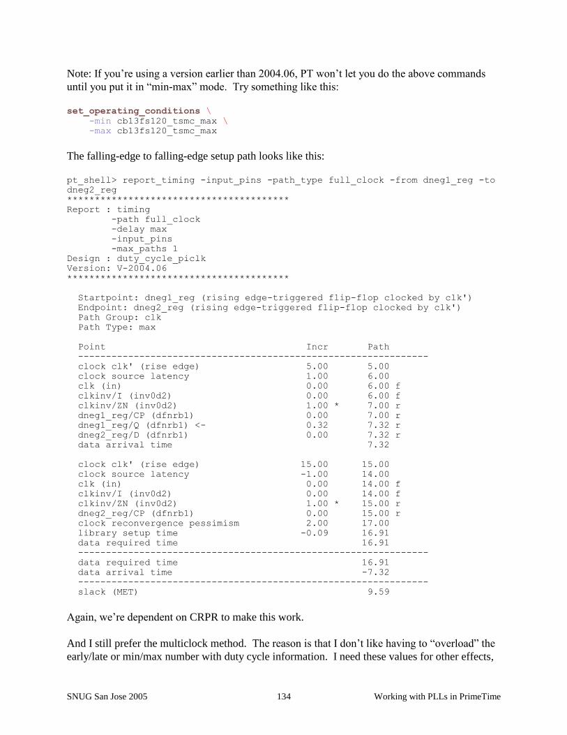
SNUG San Jose 2005 Working with PLLs in PrimeTime 134
Note: If you’re using a version earlier than 2004.06, PT won’t let you do the above commands
until you put it in “min-max” mode. Try something like this:
set_operating_conditions \
-min cb13fs120_tsmc_max \
-max cb13fs120_tsmc_max
The falling-edge to falling-edge setup path looks like this:
pt_shell> report_timing -input_pins -path_type full_clock -from dneg1_reg -to
dneg2_reg
****************************************
Report : timing
-path full_clock
-delay max
-input_pins
-max_paths 1
Design : duty_cycle_piclk
Version: V-2004.06
****************************************
Startpoint: dneg1_reg (rising edge-triggered flip-flop clocked by clk')
Endpoint: dneg2_reg (rising edge-triggered flip-flop clocked by clk')
Path Group: clk
Path Type: max
Point Incr Path
---------------------------------------------------------------
clock clk' (rise edge) 5.00 5.00
clock source latency 1.00 6.00
clk (in) 0.00 6.00 f
clkinv/I (inv0d2) 0.00 6.00 f
clkinv/ZN (inv0d2) 1.00 * 7.00 r
dneg1_reg/CP (dfnrb1) 0.00 7.00 r
dneg1_reg/Q (dfnrb1) <- 0.32 7.32 r
dneg2_reg/D (dfnrb1) 0.00 7.32 r
data arrival time 7.32
clock clk' (rise edge) 15.00 15.00
clock source latency -1.00 14.00
clk (in) 0.00 14.00 f
clkinv/I (inv0d2) 0.00 14.00 f
clkinv/ZN (inv0d2) 1.00 * 15.00 r
dneg2_reg/CP (dfnrb1) 0.00 15.00 r
clock reconvergence pessimism 2.00 17.00
library setup time -0.09 16.91
data required time 16.91
---------------------------------------------------------------
data required time 16.91
data arrival time -7.32
---------------------------------------------------------------
slack (MET) 9.59
Again, we’re dependent on CRPR to make this work.
And I still prefer the multiclock method. The reason is that I don’t like having to “overload” the
early/late or min/max number with duty cycle information. I need these values for other effects,

SNUG San Jose 2005 Working with PLLs in PrimeTime 135
and I hate to just add duty cycle into these numbers. By having separate duty cycle clocks, I can
be confident that I’m not somehow applying duty cycle variation in cases where it doesn’t belong
just because I rolled it into early/late or min/max latency.