
Wideband RF PLL fractional/integer frequency synthesizer ... · January 2016 DocID025943 Rev 7 1/58...
58
January 2016 DocID025943 Rev 7 1/58 STW81200 Wideband RF PLL fractional/integer frequency synthesizer with integrated VCOs and LDOs Datasheet - production data Features • Output frequency range: 46.875 to 6000 MHz • Very Low Noise – Normalized in band phase noise floor: -227 dBc/Hz – VCO phase noise: -135 dBc/Hz @ 1 MHz offset, 4.0 GHz carrier – Noise floor: -160 dBc/Hz • Dual architecture frequency synthesizer: Fractional-N and Integer-N • Integrated VCOs with automatic center frequency calibration • Programmable RF output dividers by 1/2/4/8/16/32/64 • Dual RF Output broadband matched with programmable power level and mute function • External VCO option with 5 V charge pump • Integrated low noise LDO voltage regulators • Maximum phase detector frequency: 100 MHz • Exact frequency mode • Fast lock and cycle slip reduction • Differential reference clock input (LVDS and LVECPL compliant) supporting up to 800 MHz • 13-bit programmable reference frequency divider • Programmable charge pump current • Digital lock detector • Integrated reference crystal oscillator core • R/W SPI interface • Logic compatibility/tolerance 1.8 V/3.3 V • Low Power Functional mode • Supply Voltage: 3.0 V to 5.4 V • Small size exposed pad VFQFPN36 package 6 x 6 x 1.0 mm • Process: BICMOS 0.25 μm SiGe Applications • Cellular/4G infrastructure equipment • Instrumentation and test equipment • Cable TV • Other wireless communication systems Description The STW81200 is a dual architecture frequency synthesizer (Fractional-N and Integer-N), that features three low phase-noise VCOs with a fundamental frequency range of 3.0 GHz to 6.0 GHz and a programmable dual RF output divider stage which allows coverage from 46.875 MHz to 6 GHz. The STW81200 optimizes size and cost of the final application thanks to the integration of low- noise LDO voltage regulators and internally- matched broadband RF outputs. The STW81200 is compatible with a wide range of supply voltages (from 3.0 V to 5.4 V) providing to the end user a very high level of flexibility which trades off excellent performance with power dissipation requirements. A low-power functional mode (software controlled) gives an extra power saving. Additional features include crystal oscillator core, external VCO mode and output-mute function. VFQFPN36 Table 1. Device summary Order Code Package Packing STW81200T VFQFPN36 Tray STW81200TR VFQFPN36 Tape and reel www.st.com
Transcript of Wideband RF PLL fractional/integer frequency synthesizer ... · January 2016 DocID025943 Rev 7 1/58...

January 2016 DocID025943 Rev 7 1/58
STW81200
Wideband RF PLL fractional/integer frequency synthesizer with integrated VCOs and LDOs
Datasheet - production data
Features
• Output frequency range: 46.875 to 6000 MHz
• Very Low Noise
– Normalized in band phase noise floor: -227 dBc/Hz
– VCO phase noise: -135 dBc/Hz @ 1 MHz offset, 4.0 GHz carrier
– Noise floor: -160 dBc/Hz
• Dual architecture frequency synthesizer: Fractional-N and Integer-N
• Integrated VCOs with automatic center frequency calibration
• Programmable RF output dividers by 1/2/4/8/16/32/64
• Dual RF Output broadband matched with programmable power level and mute function
• External VCO option with 5 V charge pump
• Integrated low noise LDO voltage regulators
• Maximum phase detector frequency: 100 MHz
• Exact frequency mode
• Fast lock and cycle slip reduction
• Differential reference clock input (LVDS and LVECPL compliant) supporting up to 800 MHz
• 13-bit programmable reference frequency divider
• Programmable charge pump current
• Digital lock detector
• Integrated reference crystal oscillator core
• R/W SPI interface
• Logic compatibility/tolerance 1.8 V/3.3 V
• Low Power Functional mode
• Supply Voltage: 3.0 V to 5.4 V
• Small size exposed pad VFQFPN36 package 6 x 6 x 1.0 mm
• Process: BICMOS 0.25 µm SiGe
Applications• Cellular/4G infrastructure equipment
• Instrumentation and test equipment
• Cable TV
• Other wireless communication systems
Description
The STW81200 is a dual architecture frequency synthesizer (Fractional-N and Integer-N), that features three low phase-noise VCOs with a fundamental frequency range of 3.0 GHz to 6.0 GHz and a programmable dual RF output divider stage which allows coverage from 46.875 MHz to 6 GHz.
The STW81200 optimizes size and cost of the final application thanks to the integration of low- noise LDO voltage regulators and internally-matched broadband RF outputs.
The STW81200 is compatible with a wide range of supply voltages (from 3.0 V to 5.4 V) providing to the end user a very high level of flexibility which trades off excellent performance with power dissipation requirements. A low-power functional mode (software controlled) gives an extra power saving.
Additional features include crystal oscillator core, external VCO mode and output-mute function.
VFQFPN36
Table 1. Device summary
Order Code Package Packing
STW81200T VFQFPN36 Tray
STW81200TR VFQFPN36 Tape and reel
www.st.com

Contents STW81200
2/58 DocID025943 Rev 7
Contents
1 Functional block diagram . . . . . . . . . . . . . . . . . . . . . . . . . . . . . . . . . . . . . 6
2 Pin definitions . . . . . . . . . . . . . . . . . . . . . . . . . . . . . . . . . . . . . . . . . . . . . . 7
3 Absolute maximum ratings . . . . . . . . . . . . . . . . . . . . . . . . . . . . . . . . . . 10
4 Operating conditions . . . . . . . . . . . . . . . . . . . . . . . . . . . . . . . . . . . . . . . 11
5 Electrical specifications . . . . . . . . . . . . . . . . . . . . . . . . . . . . . . . . . . . . . 13
6 Typical Performance Characteristics . . . . . . . . . . . . . . . . . . . . . . . . . . 19
7 Circuit description . . . . . . . . . . . . . . . . . . . . . . . . . . . . . . . . . . . . . . . . . . 24
7.1 Reference input stage . . . . . . . . . . . . . . . . . . . . . . . . . . . . . . . . . . . . . . . 24
7.2 Reference divider . . . . . . . . . . . . . . . . . . . . . . . . . . . . . . . . . . . . . . . . . . . 24
7.3 PLL N divider . . . . . . . . . . . . . . . . . . . . . . . . . . . . . . . . . . . . . . . . . . . . . . 25
7.3.1 Fractional spurs and compensation mechanism . . . . . . . . . . . . . . . . . . 26
7.4 Phase frequency detector (PFD) . . . . . . . . . . . . . . . . . . . . . . . . . . . . . . . 27
7.5 Lock detect . . . . . . . . . . . . . . . . . . . . . . . . . . . . . . . . . . . . . . . . . . . . . . . . 28
7.6 Charge pump . . . . . . . . . . . . . . . . . . . . . . . . . . . . . . . . . . . . . . . . . . . . . . 28
7.7 Fast lock mode . . . . . . . . . . . . . . . . . . . . . . . . . . . . . . . . . . . . . . . . . . . . . 29
7.8 Cycle slip reduction . . . . . . . . . . . . . . . . . . . . . . . . . . . . . . . . . . . . . . . . . 29
7.9 Voltage controlled oscillators (VCOs) . . . . . . . . . . . . . . . . . . . . . . . . . . . . 29
7.10 RF output divider stage . . . . . . . . . . . . . . . . . . . . . . . . . . . . . . . . . . . . . . 30
7.11 Low-power functional modes . . . . . . . . . . . . . . . . . . . . . . . . . . . . . . . . . . 31
7.12 LDO voltage regulators . . . . . . . . . . . . . . . . . . . . . . . . . . . . . . . . . . . . . . 31
7.13 STW81200 register programming . . . . . . . . . . . . . . . . . . . . . . . . . . . . . . 32
7.14 STW81200 register summary . . . . . . . . . . . . . . . . . . . . . . . . . . . . . . . . . . 34
7.15 STW81200 register descriptions . . . . . . . . . . . . . . . . . . . . . . . . . . . . . . . 35
7.16 Power ON sequence . . . . . . . . . . . . . . . . . . . . . . . . . . . . . . . . . . . . . . . . 50
7.17 Example of Register programming . . . . . . . . . . . . . . . . . . . . . . . . . . . . . . 50

DocID025943 Rev 7 3/58
STW81200 Contents
3
8 Application information . . . . . . . . . . . . . . . . . . . . . . . . . . . . . . . . . . . . . 51
8.1 Application diagrams . . . . . . . . . . . . . . . . . . . . . . . . . . . . . . . . . . . . . . . . 51
8.2 Thermal PCB design considerations . . . . . . . . . . . . . . . . . . . . . . . . . . . . 53
9 Evaluation Kit . . . . . . . . . . . . . . . . . . . . . . . . . . . . . . . . . . . . . . . . . . . . . 54
10 Package information . . . . . . . . . . . . . . . . . . . . . . . . . . . . . . . . . . . . . . . . 55
10.1 VFQFPN36 package information . . . . . . . . . . . . . . . . . . . . . . . . . . . . . . . 55
11 Revision history . . . . . . . . . . . . . . . . . . . . . . . . . . . . . . . . . . . . . . . . . . . 57

List of figures STW81200
4/58 DocID025943 Rev 7
List of figures
Figure 1. Functional block diagram . . . . . . . . . . . . . . . . . . . . . . . . . . . . . . . . . . . . . . . . . . . . . . . . . . . 6Figure 2. Top view . . . . . . . . . . . . . . . . . . . . . . . . . . . . . . . . . . . . . . . . . . . . . . . . . . . . . . . . . . . . . . . . 7Figure 3. VCO open-loop phase noise (5 V supply) . . . . . . . . . . . . . . . . . . . . . . . . . . . . . . . . . . . . . 19Figure 4. Closed-loop phase noise at 4.8 GHz, divided by 1 to 64 (5 V supply) . . . . . . . . . . . . . . . . 19Figure 5. VCO open-loop phase noise at 4.4 GHz vs. supply . . . . . . . . . . . . . . . . . . . . . . . . . . . . . . 19Figure 6. VCO open-loop phase noise over frequency vs. supply . . . . . . . . . . . . . . . . . . . . . . . . . . . 19Figure 7. Single sideband integrated phase noise vs. frequency and supply (FPFD= 50 MHz) . . . . . 20Figure 8. Figure of merit. . . . . . . . . . . . . . . . . . . . . . . . . . . . . . . . . . . . . . . . . . . . . . . . . . . . . . . . . . . 20Figure 9. Phase noise and fractional spurs at 2646.96 MHz vs. supply (FPFD = 61.44 MHz) . . . . . 20Figure 10. Phase noise and fractional spurs at 2118.24 MHz vs. supply (FPFD = 61.44 MHz) . . . . . 20Figure 11. Phase noise and fractional spurs at 2118.24 MHz at 5.0 V supply (FPFD = 61.44 MHz) . 20Figure 12. Phase noise and fractional spurs at 2118.24 MHz at 3.6 V supply (FPFD = 61.44 MHz) . 20Figure 13. Phase noise and fractional spurs at 2118.24 MHz at 3.0 V supply (FPFD = 61.44 MHz) . 21Figure 14. Phase noise at 5.625 GHz and 4.6 GHz (FPFD = 50 MHz) . . . . . . . . . . . . . . . . . . . . . . . . 21Figure 15. Typical VCO control voltage after VCO calibration (3.6 V supply) . . . . . . . . . . . . . . . . . . . 21Figure 16. Average KVCO over VCO frequency and supply. . . . . . . . . . . . . . . . . . . . . . . . . . . . . . . . . 21Figure 17. Output power level vs. temperature - single ended (RF_OUT_PWR=7) . . . . . . . . . . . . . . 21Figure 18. Output power level – single ended (3 dB more for differential). . . . . . . . . . . . . . . . . . . . . . 21Figure 19. Typical spur level at PFD offset over carrier frequency (5.0 V supply) . . . . . . . . . . . . . . . . 22Figure 20. Typical spur level vs. offset from 4.5 GHz (5.0 V supply, FPFD=50MHz) . . . . . . . . . . . . . . 22Figure 21. 10 kHz fractional spur (integer boundary) vs. temperature (5.0 V supply, FPFD = 50 MHz) . . . . . . . . . . . . . . . . . . . . . . . . . . . . . . . . . . . . . . . . . . . . . . . . . . . . . . . . 22Figure 22. 800 kHz fractional spur (integer boundary) vs. temperature (5.0 V supply, FPFD = 50 MHz) . . . . . . . . . . . . . . . . . . . . . . . . . . . . . . . . . . . . . . . . . . . . . . . . . . . . . . . . 22Figure 23. Frequency settling with VCO calibration – wideband view . . . . . . . . . . . . . . . . . . . . . . . . . 22Figure 24. Frequency settling with VCO calibration – narrowband view . . . . . . . . . . . . . . . . . . . . . . . 22Figure 25. Overall current consumption vs. temperature (5.0 V supply, FPFD = 50 MHz) . . . . . . . . . . 23Figure 26. Current consumption – standard vs. low power (5.0 V supply, FPFD = 50 MHz) . . . . . . . . 23Figure 27. Current consumption – standard vs. low power (3.6 V supply, FPFD = 50 MHz) . . . . . . . . 23Figure 28. Current consumption – standard vs. low power (3.0 V supply, FPFD = 50 MHz) . . . . . . . . 23Figure 29. Reference clock buffer configurations: single-ended (A), differential (B), crystal mode (C) 24Figure 30. PFD diagram. . . . . . . . . . . . . . . . . . . . . . . . . . . . . . . . . . . . . . . . . . . . . . . . . . . . . . . . . . . . 28Figure 31. SPI Protocol . . . . . . . . . . . . . . . . . . . . . . . . . . . . . . . . . . . . . . . . . . . . . . . . . . . . . . . . . . . . 32Figure 32. SPI timing diagram . . . . . . . . . . . . . . . . . . . . . . . . . . . . . . . . . . . . . . . . . . . . . . . . . . . . . . . 33Figure 33. Application diagram (internal VCO) . . . . . . . . . . . . . . . . . . . . . . . . . . . . . . . . . . . . . . . . . . 51Figure 34. Application diagram (external VCO) . . . . . . . . . . . . . . . . . . . . . . . . . . . . . . . . . . . . . . . . . . 52Figure 35. VFQFPN36 package outline . . . . . . . . . . . . . . . . . . . . . . . . . . . . . . . . . . . . . . . . . . . . . . . . 55
DocID025943 Rev 7 5/58
STW81200 List of tables
5
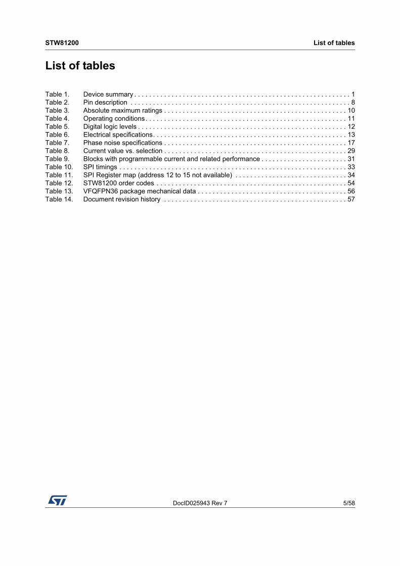
List of tables
Table 1. Device summary . . . . . . . . . . . . . . . . . . . . . . . . . . . . . . . . . . . . . . . . . . . . . . . . . . . . . . . . . . 1Table 2. Pin description . . . . . . . . . . . . . . . . . . . . . . . . . . . . . . . . . . . . . . . . . . . . . . . . . . . . . . . . . . . 8Table 3. Absolute maximum ratings . . . . . . . . . . . . . . . . . . . . . . . . . . . . . . . . . . . . . . . . . . . . . . . . . 10Table 4. Operating conditions. . . . . . . . . . . . . . . . . . . . . . . . . . . . . . . . . . . . . . . . . . . . . . . . . . . . . . 11Table 5. Digital logic levels . . . . . . . . . . . . . . . . . . . . . . . . . . . . . . . . . . . . . . . . . . . . . . . . . . . . . . . . 12Table 6. Electrical specifications. . . . . . . . . . . . . . . . . . . . . . . . . . . . . . . . . . . . . . . . . . . . . . . . . . . . 13Table 7. Phase noise specifications . . . . . . . . . . . . . . . . . . . . . . . . . . . . . . . . . . . . . . . . . . . . . . . . . 17Table 8. Current value vs. selection . . . . . . . . . . . . . . . . . . . . . . . . . . . . . . . . . . . . . . . . . . . . . . . . . 29Table 9. Blocks with programmable current and related performance . . . . . . . . . . . . . . . . . . . . . . . 31Table 10. SPI timings . . . . . . . . . . . . . . . . . . . . . . . . . . . . . . . . . . . . . . . . . . . . . . . . . . . . . . . . . . . . . 33Table 11. SPI Register map (address 12 to 15 not available) . . . . . . . . . . . . . . . . . . . . . . . . . . . . . . 34Table 12. STW81200 order codes . . . . . . . . . . . . . . . . . . . . . . . . . . . . . . . . . . . . . . . . . . . . . . . . . . . 54Table 13. VFQFPN36 package mechanical data . . . . . . . . . . . . . . . . . . . . . . . . . . . . . . . . . . . . . . . . 56Table 14. Document revision history . . . . . . . . . . . . . . . . . . . . . . . . . . . . . . . . . . . . . . . . . . . . . . . . . 57

Functional block diagram STW81200
6/58 DocID025943 Rev 7
1 Functional block diagram
Figure 1. Functional block diagram

DocID025943 Rev 7 7/58
STW81200 Pin definitions
57
2 Pin definitions
Figure 2. Top view
VIN
_LD
O_4
V5
CBYP_4V5 1
VREG_4V5 2
VCC_VCO_Core 3
HW_PD 4
PDRF1 5
PDRF2/FL_SW 6
CBYP 7
36
TE
ST
_SE
3
5
RF
2_O
UT
P
34
RF
2_O
UT
N
33
VC
C_R
FO
UT
3
2
RF
1_O
UT
P
31
RF
1_O
UT
N
30
27
26
25
24
23
22
21
10
11
12
13
14
15
16
VREG_DIG
VDD_DSM_NDIV
LE
SCK
SDI
LD_SDO
REF_CLKP
VR
VC
TR
L
EX
TV
CO
_IN
P
EX
TV
CO
_IN
N
VD
D_
CP
ICP
VC
C_
CP
OU
T
8
9
VREG_VCO
VIN_LDO_VCO
VR
EG
_RF
29
VIN
_LD
O_
RF
_DIG
28
17
18
VD
D_P
FD
VIN
_LD
O_
RE
F20
19
REF_CLKN
VREG_REF

Pin definitions STW81200
8/58 DocID025943 Rev 7
Table 2. Pin description
Pin No Name Description Observation
1 CBYP_4V5Connection for 4.5 V regulator
bypass capacitor-
2 VREG_4V5Regulated output voltage for 4.5V
regulatorAdjustable output voltage: 5.0 V, 4.5 V, 2.6 V, 3.3 V
3 VCC_VCO_Core Supply voltage for VCO CoreMust be connected to VREG_4V5 or VREG_VCO
4 HW_PD HW Power DownCMOS Schmitt Triggered Input, 1.8 V
compatible, 3.3 V tolerant
5 PD_RF1RF1 output stage Power Down
control
CMOS Schmitt Triggered Input, 1.8 V
compatible, 3.3 V tolerant
6 PD_RF2/FL_SWRF2 output stage Power Down
Control / Fast Lock switch
CMOS Schmitt Triggered Input, 1.8 V
compatible, 3.3V tolerant (with Fast lock feature disabled); High impedance/ GND shorted output (with Fast Lock feature enabled)
7 CBYPConnection for VCO circuitry
regulator bypass capacitor-
8 VREG_VCORegulated output voltage for VCO
circuitry regulator-
9 VIN_LDO_VCOSupply voltage for VCO circuitry
regulator-
10 VRConnection for reference voltage
filtering capacitor-
11 VCTRL VCO control voltage -
12 EXTVCO_INP External VCO positive inputThis pin must be connected to ground if external VCO is not used
13 EXTVCO_INN External VCO negative inputThis pin must be connected to ground if external VCO is not used
14 VDD_CPSupply voltage for Charge Pump bias
This pin must be connected to VREG_VCO
15 ICP PLL charge pump output -
16 VCC_CPOUTSupply voltage for Charge Pump output stage
This pin must be connected to VREG_4V5 or VREG_VCO
17 VDD_PFD Supply voltage for PFDThis pin must be connected to VREG_REF
18 VIN_LDO_REF Supply voltage for PLL regulator -
19 VREG_REFRegulated output voltage for Reference Clock regulator
-
20 REF_CLKN Reference clock negative input -
21 REF_CLKP Reference clock positive input -
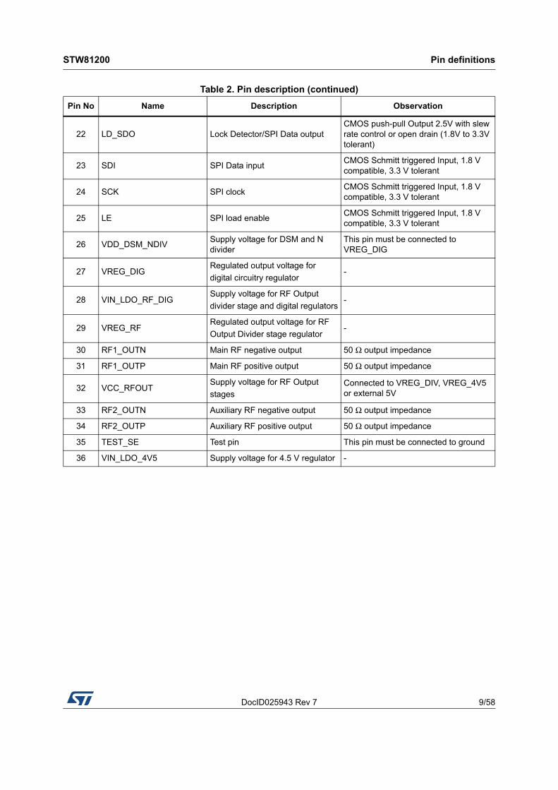
DocID025943 Rev 7 9/58
STW81200 Pin definitions
57
22 LD_SDO Lock Detector/SPI Data outputCMOS push-pull Output 2.5V with slew rate control or open drain (1.8V to 3.3V tolerant)
23 SDI SPI Data inputCMOS Schmitt triggered Input, 1.8 V compatible, 3.3 V tolerant
24 SCK SPI clockCMOS Schmitt triggered Input, 1.8 V compatible, 3.3 V tolerant
25 LE SPI load enableCMOS Schmitt triggered Input, 1.8 V compatible, 3.3 V tolerant
26 VDD_DSM_NDIVSupply voltage for DSM and N divider
This pin must be connected to VREG_DIG
27 VREG_DIGRegulated output voltage for
digital circuitry regulator -
28 VIN_LDO_RF_DIGSupply voltage for RF Output
divider stage and digital regulators-
29 VREG_RFRegulated output voltage for RF
Output Divider stage regulator -
30 RF1_OUTN Main RF negative output 50 Ω output impedance
31 RF1_OUTP Main RF positive output 50 Ω output impedance
32 VCC_RFOUTSupply voltage for RF Output
stagesConnected to VREG_DIV, VREG_4V5 or external 5V
33 RF2_OUTN Auxiliary RF negative output 50 Ω output impedance
34 RF2_OUTP Auxiliary RF positive output 50 Ω output impedance
35 TEST_SE Test pin This pin must be connected to ground
36 VIN_LDO_4V5 Supply voltage for 4.5 V regulator -
Table 2. Pin description (continued)
Pin No Name Description Observation

Absolute maximum ratings STW81200
10/58 DocID025943 Rev 7
3 Absolute maximum ratings
Table 3. Absolute maximum ratings
Symbol Parameter Value Unit
VCC
Supply voltage pins #14, #17, #26 -0.3 to 2.7 V
Supply voltage LDOs pins #9, #18, #28, #36 -0.3 to 5.4 V
Supply voltage pins #3 -0.3 to 5 V
Supply voltage pins #16, #32 -0.3 to 5.4 V
Tstg Storage temperature +150 °C
ESD
Electrical Static Discharge
HBM(1)
CDM-JEDEC Standard
MM
2
0.5
0.2
kV
1. The maximum rating of the ESD protection circuitry on pin 21 (REF_CLKP) is 1.5 kV.

DocID025943 Rev 7 11/58
STW81200 Operating conditions
57
4 Operating conditions
Table 4. Operating conditions
Symbol Parameter Test conditions Min Typ Max Unit
VCC
Supply voltage pins #14, #17, #26
- 2.5 - 2.7 V
Supply voltage (LDOs inputs) pins #9, #18, #28, #36
- 3.0 - 5.4 V
Supply voltage pin #3, #16, #32 - 2.5 - 5 V
ICC
Current Consumption Pin #3, #16 and #32 supplied at 4.5 V
DIV2 ON, Main Output only, 4 GHz VCO, max. performance
- 84 - mA
Current Consumption Pin #3, #16 and #32 supplied at 2.6 V
- 50 - mA
Current consumption other blocks an supplies at 2.6 V
- 110 - mA
TA Operating ambient temperature - -40 - 85 °C
TJ Maximum junction temperature - - - 125 °C
ΘJAJunction to ambient package thermal resistance(1) Multilayer JEDEC board - 33 - °C/W
ΘJBJunction to board package thermal resistance(1) Multilayer JEDEC board - 18 - °C/W
ΘJCJunction to case package thermal resistance(1) Multilayer JEDEC board - 3 - °C/W
ΨJBThermal characterization parameter junction to board(1) Multilayer JEDEC board - 17 - °C/W
ΨJTThermal characterization parameter junction to top case(1) Multilayer JEDEC board - 0.3 - °C/W
1. Refer to JEDEC standard JESD 51-12 for a detailed description of the thermal resistances and thermal parameters. Data here presented are referring to a Multilayer board according to JEDEC standard. TJ = TA + ΘJA * Pdiss (in order to estimate TJ if ambient temperature TA and dissipated power Pdiss are known) TJ = TB + ΨJB * Pdiss (in order to estimate TJ if ambient temperature TB and dissipated power Pdiss are known) TJ = TT + ΨJT * Pdiss (in order to estimate TJ if ambient temperature TT and dissipated power Pdiss are known)
Operating conditions STW81200
12/58 DocID025943 Rev 7
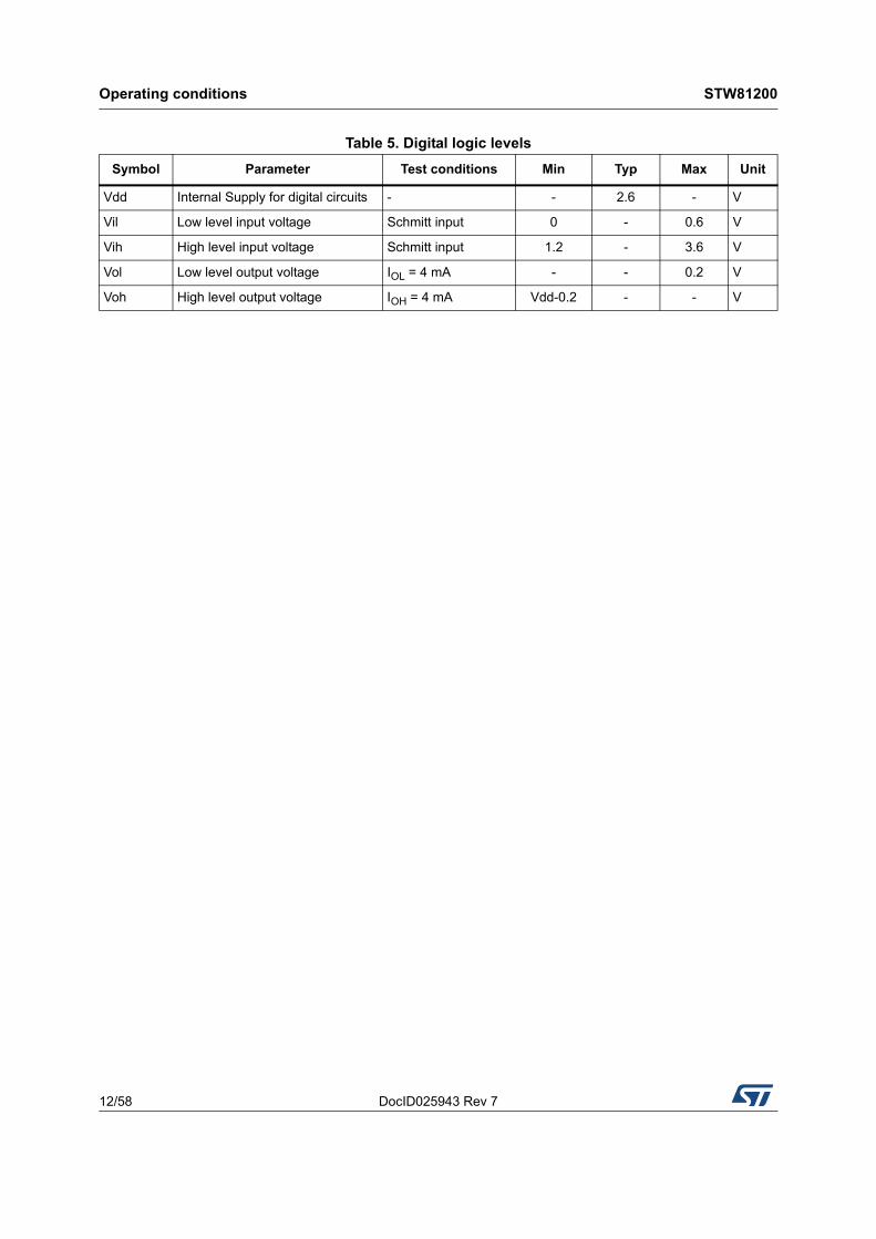
Table 5. Digital logic levels
Symbol Parameter Test conditions Min Typ Max Unit
Vdd Internal Supply for digital circuits - - 2.6 - V
Vil Low level input voltage Schmitt input 0 - 0.6 V
Vih High level input voltage Schmitt input 1.2 - 3.6 V
Vol Low level output voltage IOL = 4 mA - - 0.2 V
Voh High level output voltage IOH = 4 mA Vdd-0.2 - - V

DocID025943 Rev 7 13/58
STW81200 Electrical specifications
57
5 Electrical specifications
All electrical specifications are given at 25oC TAMB and in a full-current mode, unless otherwise stated.
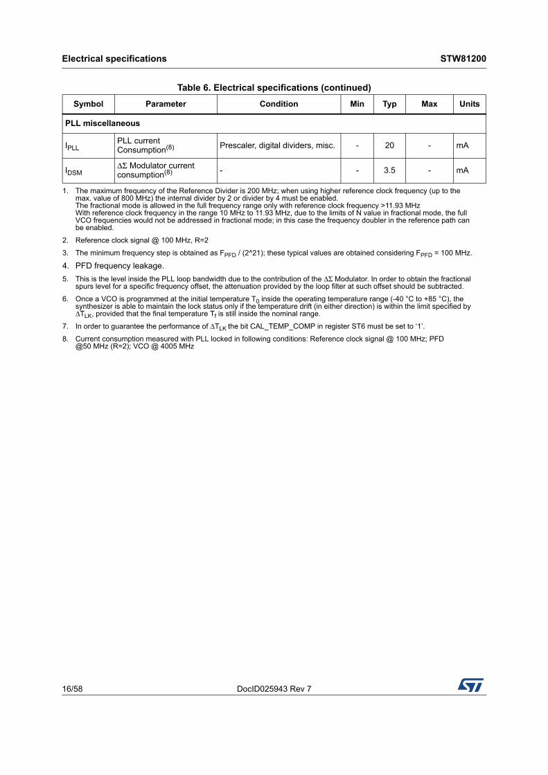
Table 6. Electrical specifications
Symbol Parameter Condition Min Typ Max Units
Output frequency range
FOUT Output Frequency
Direct output 3000 - 6000 MHz
Divider by 2 output 1500 - 3000 MHz
… … - … MHz
Divider by 64 output 46.875 - 93.75 MHz
VCO dividers
N VCO Divider Ratio
Integer Mode 24 - 131071 -
Fractional mode (DSM 1st Order)
24 - 510 -
Fractional mode (DSM 2nd Order)
25 - 509 -
Fractional mode (DSM 3rd Order)
27 - 507 -
Fractional mode (DSM 4st Order)
31 - 503 -
Xtal oscillator
FXTAL XTAL frequency range - 10 - 50 MHz
ESRXTAL XTAL ESR - - - 50 Ω
PXTAL XTAL Power Dissipation - - - 5 mW
CINXTALXTAL Oscillator Input capacitance
Single ended 0.6 - - pF
PNXTALXTAL Oscillator Phase Noise Floor
50 MHz XTAL - -162 - dBc/Hz
TOLXTAL XTAL Oscillator accuracy @12 MHz, 25 ºC - - 10 ppm
Reference clock and phase frequency detector
Fref
Reference input frequency(1) - 10 - 800 MHz
Reference input sensitivityDifferential Mode 0.2 1 1.25 Vp
Single Ended Mode 0.35 1 1.25 Vp
PNREFINReference Input Buffer Phase Noise Floor
Single Ended Mode @100 MHz, sinusoidal signal 1.25 Vp
- -163 - dBc/Hz
LVDS signal @100 MHz 400 mVp
- -159 - dBc/Hz
Electrical specifications STW81200
14/58 DocID025943 Rev 7
IREF Current consumption(2)
Differential Mode - 10 -
mASingle Ended Mode - 3 -
XTAL oscillator Mode - 5 -
R Reference Divider Ratio - 1 - 8191
FPFD PFD input frequency(3) - - - 100 MHz
FSTEP Frequency step(3)
LO direct output - 47.5 - Hz
LO with divider by 2 - 23.75 - Hz
… - … - Hz
LO with divider by 64 - 0.7422 - Hz
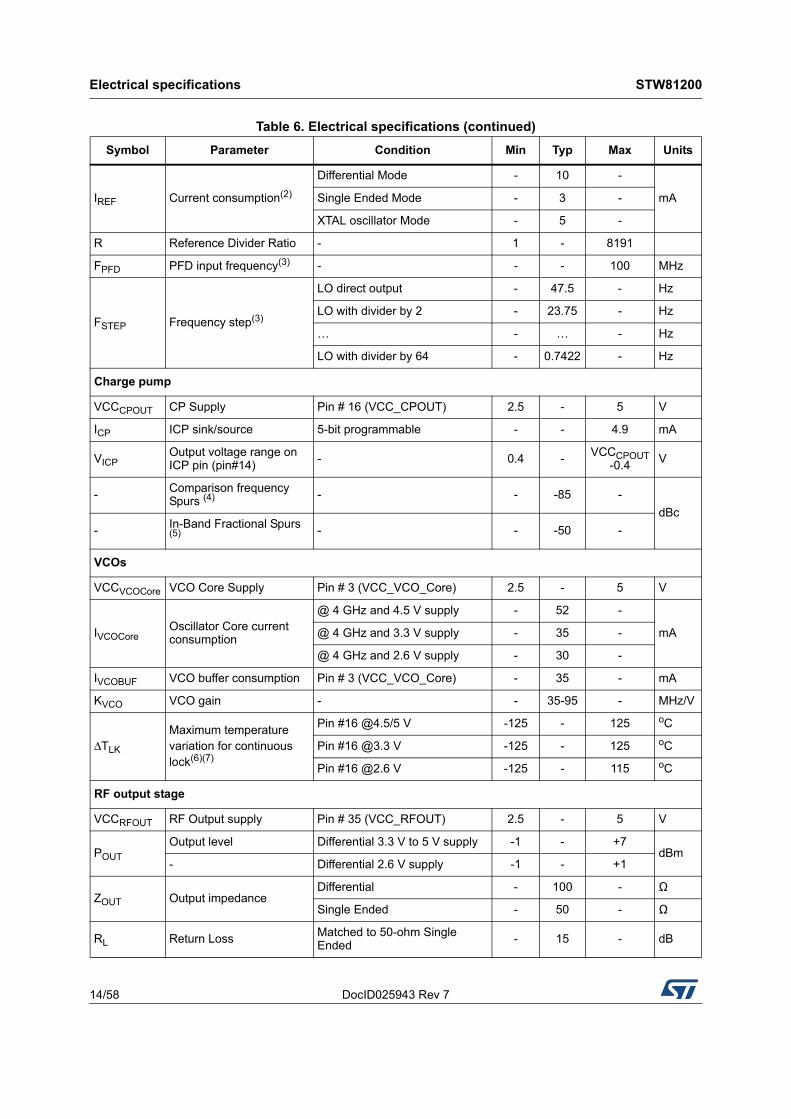
Charge pump
VCCCPOUT CP Supply Pin # 16 (VCC_CPOUT) 2.5 - 5 V
ICP ICP sink/source 5-bit programmable - - 4.9 mA
VICPOutput voltage range on ICP pin (pin#14) - 0.4 -
VCCCPOUT-0.4 V
-Comparison frequency Spurs (4) - - -85 -
dBc
-In-Band Fractional Spurs (5) - - -50 -
VCOs
VCCVCOCore VCO Core Supply Pin # 3 (VCC_VCO_Core) 2.5 - 5 V
IVCOCoreOscillator Core current consumption
@ 4 GHz and 4.5 V supply - 52 -
mA@ 4 GHz and 3.3 V supply - 35 -
@ 4 GHz and 2.6 V supply - 30 -
IVCOBUF VCO buffer consumption Pin # 3 (VCC_VCO_Core) - 35 - mA
KVCO VCO gain - - 35-95 - MHz/V
ΔTLK
Maximum temperaturevariation for continuouslock(6)(7)
Pin #16 @4.5/5 V -125 - 125 oC
Pin #16 @3.3 V -125 - 125 oC
Pin #16 @2.6 V -125 - 115 oC
RF output stage
VCCRFOUT RF Output supply Pin # 35 (VCC_RFOUT) 2.5 - 5 V
POUT
Output level Differential 3.3 V to 5 V supply -1 - +7dBm
- Differential 2.6 V supply -1 - +1
ZOUT Output impedanceDifferential - 100 - Ω
Single Ended - 50 - Ω
RL Return Loss Matched to 50-ohm Single Ended
- 15 - dB
Table 6. Electrical specifications (continued)
Symbol Parameter Condition Min Typ Max Units

DocID025943 Rev 7 15/58
STW81200 Electrical specifications
57
H2 LO 2nd Harmonic
Direct output (single/differential) - -30/-40 - dBc
Divided output (single/differential) - -30/-35 - dBc
H3 LO 3rd Harmonic
Direct output (single/differential) - -15/-15 - dBc
Divided output (single/differential)
- -15/-15 - dBc
PMUTELevel of Signal with RF Mute Enabled
Direct output @4 GHz (single/diff)
- -45/-60 - dBm
Divided output @2 GHz (single/diff)
- -45/-60 - dBm
PISO Main/aux port isolation
Direct output @4 GHz (single/diff)
- -35/-40 - dBc
Divided output @2 GHz (single/diff) - -40/-45 - dBc
IDIVRF Divider Current Consumption(8)
Direct output (1 differential output) - 28 -
mA
DIV2 buff (1 differential output) - 47 -
DIV4 buff (1 differential output) - 56 -
DIV8 buff (1 differential output) - 65 -
DIV16 buff (1 differential output) - 75 -
DIV32 buff (1 differential output) - 83
DIV64 buff (1 differential output) - 92 -
Auxiliary path enabled - 19 -
IRFOUTBUFRF Output Buffer Current Consumption(8)
3.3 V to 5 V supply (1 differential output; POUT = +7 dBm)
- 25 -
mA3.3 V to 5 V Auxiliary path enabled - 25 -
2.6 V supply (1 differential output; POUT = +1 dBm) - 12 -
2.6 V Auxiliary path enabled - 12 -
Table 6. Electrical specifications (continued)
Symbol Parameter Condition Min Typ Max Units
Electrical specifications STW81200
16/58 DocID025943 Rev 7
PLL miscellaneous
IPLLPLL current Consumption(8) Prescaler, digital dividers, misc. - 20 - mA
IDSMΔΣ Modulator current consumption(8) - - 3.5 - mA
1. The maximum frequency of the Reference Divider is 200 MHz; when using higher reference clock frequency (up to the max. value of 800 MHz) the internal divider by 2 or divider by 4 must be enabled. The fractional mode is allowed in the full frequency range only with reference clock frequency >11.93 MHz With reference clock frequency in the range 10 MHz to 11.93 MHz, due to the limits of N value in fractional mode, the full VCO frequencies would not be addressed in fractional mode; in this case the frequency doubler in the reference path can be enabled.
2. Reference clock signal @ 100 MHz, R=2
3. The minimum frequency step is obtained as FPFD / (2^21); these typical values are obtained considering FPFD = 100 MHz.
4. PFD frequency leakage.
5. This is the level inside the PLL loop bandwidth due to the contribution of the ΔΣ Modulator. In order to obtain the fractional spurs level for a specific frequency offset, the attenuation provided by the loop filter at such offset should be subtracted.
6. Once a VCO is programmed at the initial temperature T0 inside the operating temperature range (-40 °C to +85 °C), the synthesizer is able to maintain the lock status only if the temperature drift (in either direction) is within the limit specified by ΔTLK, provided that the final temperature Tf is still inside the nominal range.
7. In order to guarantee the performance of ΔTLK the bit CAL_TEMP_COMP in register ST6 must be set to ‘1’.
8. Current consumption measured with PLL locked in following conditions: Reference clock signal @ 100 MHz; PFD @50 MHz (R=2); VCO @ 4005 MHz
Table 6. Electrical specifications (continued)
Symbol Parameter Condition Min Typ Max Units
DocID025943 Rev 7 17/58
STW81200 Electrical specifications
57
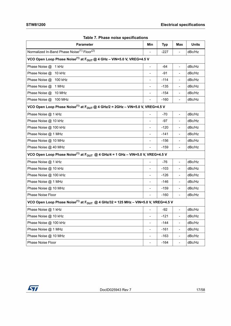
Table 7. Phase noise specifications
Parameter Min Typ Max Units
Normalized In-Band Phase Noise(1) Floor(2) - -227 - dBc/Hz
VCO Open Loop Phase Noise(1) at FOUT @ 4 GHz – VIN=5.0 V, VREG=4.5 V
Phase Noise @ 1 kHz - -64 - dBc/Hz
Phase Noise @ 10 kHz - -91 - dBc/Hz
Phase Noise @ 100 kHz - -114 - dBc/Hz
Phase Noise @ 1 MHz - -135 - dBc/Hz
Phase Noise @ 10 MHz - -154 - dBc/Hz
Phase Noise @ 100 MHz - -160 - dBc/Hz
VCO Open Loop Phase Noise(1) at FOUT @ 4 GHz/2 = 2GHz – VIN=5.0 V, VREG=4.5 V
Phase Noise @ 1 kHz - -70 - dBc/Hz
Phase Noise @ 10 kHz - -97 - dBc/Hz
Phase Noise @ 100 kHz - -120 - dBc/Hz
Phase Noise @ 1 MHz - -141 - dBc/Hz
Phase Noise @ 10 MHz - -156 - dBc/Hz
Phase Noise @ 40 MHz - -159 - dBc/Hz
VCO Open Loop Phase Noise(1) at FOUT @ 4 GHz/4 = 1 GHz – VIN=5.0 V, VREG=4.5 V
Phase Noise @ 1 kHz - -76 - dBc/Hz
Phase Noise @ 10 kHz - -103 - dBc/Hz
Phase Noise @ 100 kHz - -126 - dBc/Hz
Phase Noise @ 1 MHz - -146 - dBc/Hz
Phase Noise @ 10 MHz - -159 - dBc/Hz
Phase Noise Floor - -160 - dBc/Hz
VCO Open Loop Phase Noise(1) at FOUT @ 4 GHz/32 = 125 MHz – VIN=5.0 V, VREG=4.5 V
Phase Noise @ 1 kHz - -92 - dBc/Hz
Phase Noise @ 10 kHz - -121 - dBc/Hz
Phase Noise @ 100 kHz - -144 - dBc/Hz
Phase Noise @ 1 MHz - -161 - dBc/Hz
Phase Noise @ 10 MHz - -163 - dBc/Hz
Phase Noise Floor - -164 - dBc/Hz

Electrical specifications STW81200
18/58 DocID025943 Rev 7
VCO Open Loop Phase Noise(1) at FOUT @ 4 GHz – VIN=3.6V , VREG=3.3 V
Phase Noise @ 1 kHz - -62 - dBc/Hz
Phase Noise @ 10 kHz - -89 - dBc/Hz
Phase Noise @ 100 kHz - -113.2 - dBc/Hz
Phase Noise @ 1 MHz - -133.6 - dBc/Hz
Phase Noise @ 10 MHz - -152.4 - dBc/Hz
Phase Noise @ 100 MHz - -158.5 - dBc/Hz
VCO Open Loop Phase Noise(1) at FOUT @ 4 GHz – VIN=3.0 V, VREG=2.6 V
Phase Noise @ 1 kHz - -60.5 - dBc/Hz
Phase Noise @ 10 kHz - -88 - dBc/Hz
Phase Noise @ 100 kHz - -110.3 - dBc/Hz
Phase Noise @ 1 MHz - -131 - dBc/Hz
Phase Noise @ 10 MHz - -150 - dBc/Hz
Phase Noise @ 100 MHz - -157 - dBc/Hz
1. Phase Noise SSB unless otherwise specified. The VCO Open loop figures are specified at 4.5/5 V on VCC_VCO_Core (pin #3).
2. Normalized PN = Measured PN – 20log(N) – 10log(FPFD) where N is the VCO divider ratio and FPFD is the comparison frequency at the PFD input.
Table 7. Phase noise specifications
Parameter Min Typ Max Units

DocID025943 Rev 7 19/58
STW81200 Typical Performance Characteristics
57
6 Typical Performance Characteristics
Figure 3. VCO open-loop phase noise (5 V supply)
Figure 4. Closed-loop phase noise at 4.8 GHz, divided by 1 to 64 (5 V supply)
Figure 5. VCO open-loop phase noise at 4.4 GHz vs. supply
Figure 6. VCO open-loop phase noise over frequency vs. supply

Typical Performance Characteristics STW81200
20/58 DocID025943 Rev 7
Figure 7. Single sideband integrated phase noise vs. frequency and supply (FPFD= 50 MHz)
Figure 8. Figure of merit
Figure 9. Phase noise and fractional spurs at 2646.96 MHz vs. supply (FPFD = 61.44 MHz)
Figure 10. Phase noise and fractional spurs at 2118.24 MHz vs. supply (FPFD = 61.44 MHz)
Figure 11. Phase noise and fractional spurs at 2118.24 MHz at 5.0 V supply (FPFD = 61.44 MHz)
Figure 12. Phase noise and fractional spurs at 2118.24 MHz at 3.6 V supply (FPFD = 61.44 MHz)

DocID025943 Rev 7 21/58
STW81200 Typical Performance Characteristics
57
Figure 13. Phase noise and fractional spurs at 2118.24 MHz at 3.0 V supply (FPFD = 61.44 MHz)
Figure 14. Phase noise at 5.625 GHz and 4.6 GHz (FPFD = 50 MHz)
Figure 15. Typical VCO control voltage after VCO calibration (3.6 V supply)
Figure 16. Average KVCO over VCO frequency and supply
Figure 17. Output power level vs. temperature - single ended (RF_OUT_PWR=7)
Figure 18. Output power level – single ended (3 dB more for differential)

Typical Performance Characteristics STW81200
22/58 DocID025943 Rev 7
Figure 19. Typical spur level at PFD offset over carrier frequency (5.0 V supply)
Figure 20. Typical spur level vs. offset from 4.5 GHz (5.0 V supply, FPFD=50MHz)
Figure 21. 10 kHz fractional spur (integer boundary) vs. temperature
(5.0 V supply, FPFD = 50 MHz)
Figure 22. 800 kHz fractional spur (integer boundary) vs. temperature
(5.0 V supply, FPFD = 50 MHz)
Figure 23. Frequency settling with VCO calibration – wideband view
Figure 24. Frequency settling with VCO calibration – narrowband view

DocID025943 Rev 7 23/58
STW81200 Typical Performance Characteristics
57
Figure 25. Overall current consumption vs. temperature (5.0 V supply, FPFD = 50 MHz)
Figure 26. Current consumption – standard vs. low power (5.0 V supply, FPFD = 50 MHz)
Figure 27. Current consumption – standard vs. low power (3.6 V supply, FPFD = 50 MHz)
Figure 28. Current consumption – standard vs. low power (3.0 V supply, FPFD = 50 MHz)

Circuit description STW81200
24/58 DocID025943 Rev 7
7 Circuit description
7.1 Reference input stage
The reference input stage provides different modes for the reference clock signal.
Both single-ended and differential modes (LVDS, LVECPL) are supported; a crystal mode is also provided in order to build a Pierce type crystal oscillator. Figure 29 shows the connections required for the different configurations supported.
In single-ended and differential modes the inputs must be AC coupled as the REF_CLKP and REF_CLKN pins are internally biased to an optimal DC operating point. The input resistance is 100 ohms differential and the best performance for phase noise is obtained for signals with a higher slew rate, such as a square wave.
Figure 29. Reference clock buffer configurations: single-ended (A), differential (B), crystal mode (C)
7.2 Reference divider
The 13-bit programmable reference counter is used to divide the input reference frequency to the desired PFD frequency. The division ratio is programmable from 1 to 8191.
The maximum allowed input frequency of the R-Counter is 200 MHz.
The reference clock can be extended up to 400 MHz enabling the divide-by-2 stage or up to 800 MHz enabling the divide-by-4 stage.
A frequency doubler is provided in order to double low reference frequencies and increase the PFD operating frequency thus allowing an easier filtering of the out-of-band noise of the Delta-Sigma Modulator; the doubler is introducing a noise degradation in the in-band PLL noise thus this feature should be carefully used.
When the doubler is enabled, the maximum reference frequency is limited to 25 MHz.
REF_CLKP
REF_CLKN
REF_CLKP
REF_CLKN
REF_CLKP
REF_CLKN
100 Ω
A) B) C)

DocID025943 Rev 7 25/58
STW81200 Circuit description
57
7.3 PLL N divider
The N divider sets the division ratio in the PLL feedback path.
Both Integer-N and Fractional-N PLL architectures are implemented in order to ensure the best overall performance of the synthesizer.
The Fractional-N division is achieved combining the integer divider section with a Delta-Sigma modulator (DSM) which sets the fractional part of the overall division ratio.
The DSM is implemented as a MASH structure with programmable order (2 bit; 1st, 2nd, 3rd
and 4th order), programmable MODULUS (21 bit).
It includes also a DITHERING function (1 bit) which can be used to reduce fractional spur tones by spreading the DSM sequence and consequently the energy of the spurs over a wider bandwidth.
The overall division ratio N is given by:
The integer part NINT is 17-bit programmable and can range from 24 to 131071 in Integer Mode. For NINT ≥ 512 the fractional mode is not allowed and the setting used for DSM does not have any effect.
Based upon the selected order of the Delta-Sigma Modulator the allowed range of NINTvalues changes as follows:
• 24 to 510 - 1st Order DSM
• 25 to 509 - 2nd Order DSM
• 27 to 507 - 3rd Order DSM
• 31 to 503 - 4th Order DSM
The fractional part NFRAC of the division ratio is controlled by setting the values FRAC and MOD (21 bits each) and it depends also on the value of DITHERING (1 bit):
The MOD value can range from 2 to 2097151, while the range of FRAC is from 0 to MOD-1. If the DITHERING function is not used (DITHERING=0) the fractional part of N is simply achieved as ratio of FRAC over MOD.
N NINT NFRAC+=
NFRACFRACMOD-----------------
DITHERING2 MOD⋅
-----------------------------------+=
Circuit description STW81200
26/58 DocID025943 Rev 7
The resulting VCO frequency is:
where:
FVCO is the output frequency of VCO
Fref is the input reference frequency
R is the division ratio of reference chain
N is the overall division ratio of the PLL
The implementation with programmable modulus allows the user to select easily the desired fraction and the exact synthesized frequency without any approximation.
The MOD value can be set to very high values thus the frequency resolution of the synthesizer can reach very fine steps (down to a few hertz).
A ‘low spur mode’ could be configured by maximizing both FRAC and MOD values, keeping the same desired FRAC/MOD ratio, and setting the DITHERING bit to ‘1’. The drawback is a small frequency error, equal to FPFD/(2*MOD), on the synthesized frequency which is in the range of a few hertz, usually tolerated by most applications.
7.3.1 Fractional spurs and compensation mechanism
The fractional PLL operation generates unwanted fractional spurs around the synthesized frequency.
The integer boundary spurs occur when the carrier frequency is close to an integer multiple of the PFD frequency. If the frequency difference between the carrier and the N*FPFD falls inside the PLL loop bandwidth, the integer boundary spur is unfiltered and represents the worst case situation giving the highest spur level.
The channel spurs are generated by the delta-sigma modulator operations and depend on its settings (they are mainly related to the MOD value). The channel spurs appear at a frequency offset from the carrier, equal to FPFD/MOD and its harmonics, and they are not integer boundary. If the MOD value is extremely high (close to the maximum value of 221-1) the channel spur offset is of the order of a tenth of a Hertz and it appears as ‘granular noise’ shaped by the PLL around the carrier.
The STW81200 provides the user with three different mechanisms to compensate fractional spurs: PFD delay mode, charge pump leakage current and down-split current. These features should be adopted case-by-case as they give different results spur-level results depending on setup conditions (reference clock frequency, PFD frequency, DSM setup, VCO frequency, carrier frequency, charge pump current, VCO/charge pump supply voltage).
PFD delay mode
The STW81200 implements two programmable differentiated delay lines in the reset path of the main flip-flop of the PFD. This allow different delay reset values to be set for VCO divided path and reference-clock divided path, allowing an offset value to be forced on the PFD and charge-pump characteristics, far enough from the zero in order to guarantee that the whole circuit works in a more linear region.
FVCO
Fref
R---------- N⋅
Fref
R---------- NINT
FRACMOD-----------------
DITHERING2 MOD⋅
-----------------------------------+ + ⋅= =

DocID025943 Rev 7 27/58
STW81200 Circuit description
57
It is possible to set the sign of the delay through the PFD_DEL_MODE bit in the ST3 Register (no delay, VCO_DIV_delayed or REF_DIV_delayed). The delay value can be set through the PFD_DEL bit in the ST0 Register (2 bit; 0=1.2 ns, 1=1.9 ns, 2=2.5 ns, 3=3.0 ns). Even though the for spur-compensation settings are best optimized case-by-case, the setup ‘VCO_DIV_delayed + 1.2 ns delay’ is strongly recommended for most conditions.
Charge pump leakage current
A different way to force an offset value on the PFD+CP characteristics is provided within the STW81200 by sourcing or sinking a DC leakage current from the charge pump (settings available in the ST3 Register). The leakage current is 5-bit programmable starting from a base DC current of 10 µA (it can be doubled to 20 uA by setting bit CP_LEAK_x2 = 1b). The sign is set by CP_LEAK_DIR bit: 0b = down-leakage (sink), 1b = up-leakage (source).
The resulting delay offset can be calculated as follows:
Experimental results show that down-leakage currents are more effective than up-leakage. The user must be aware that the use of the leakage current mechanism might impact the overall phase noise performance by increasing the charge pump noise contribution.
Down-split current
This mechanism is enabled through the DNSPLIT_EN bit (ST3 Register), is the injection of a down-split current pulse from the charge pump circuit. The current pulse is 16 VCO cycles wide while the current level is set by the PFD_DEL bit (ST0 Register) among 4 different possible values: 0, 0.25*ICP, 0.5*ICP or 0.75*ICP.
7.4 Phase frequency detector (PFD)
The PFD takes inputs from the reference and the VCO dividers and produces an output proportional to the phase error. The PFD includes a delay gate that controls the width of the anti-backlash pulse (1.2 to 3 ns). This pulse ensures that there is no dead zone in the PFD transfer function.
Figure 30 shows a simplified schematic of the PFD.
delayILEAK
FPFD ICP⋅---------------------------=

Circuit description STW81200
28/58 DocID025943 Rev 7
Figure 30. PFD diagram
7.5 Lock detect
The lock detector indicates the lock state for the PLL. The lock condition is detected by comparing the UP and DOWN outputs of the digital Phase Frequency Detector
A CMOS logic output signal indicates the lock state; the polarity of the output signal can be inverted using the LD_ACTIVELOW bit.
The lock condition occurs when the delay between the edges of UP and DOWN signals is lower than a specific value (3-bit programmable from 2 ns to 16 ns) and this condition is stable for a specific number of consecutive PFD cycles (3-bit programmable counter from 4 to 4096 cycles).
This flexibility is needed by the lock detector circuitry to work properly with all the possible different PLL setups (Integer-N, Fractional-N, different PFD frequencies and so on).
7.6 Charge pump
This block drives two matched current sources, Iup and Idown, which are controlled respectively by the UP and DOWN PFD outputs. The nominal value of the output current (ICP) can be set by a 5-bit word.
The minimum value of the output current (ICP) is 158 µA.
The charge pump also includes a compensation circuit to take into account the KVCO variation versus VCO control voltage, which changes with temperature and process for a specified frequency. The KVCO compensation block adjusts the nominal ICP value, minimizing the variation of the product ICP x KVCO to keep the PLL bandwidth constant for the specified frequency.
In order to compensate the change of KVCO over frequency, the user should manually adjust the ICP value to keep the PLL bandwidth constant.
In addition, the charge-pump output stage can operate with a 2.5 V to 5.0 V supply voltage. The LDO_4V5 regulator, programmable at 2.6 V, 3.3 V and 4.5 V, can be used for this purpose. The CP_SUPPLY_MODE[1:0] field (ST4 Register) must be set according to the supply voltage.
Up
Down
ABL
Delay
DFF
R
R
DFF
VDD
Fref
Fref
VDD

DocID025943 Rev 7 29/58
STW81200 Circuit description
57
7.7 Fast lock mode
The fast-lock feature can be enabled to trade fast settling time with spurs rejection, performances which generally require different settings of PLL bandwidth (narrow for better spurs rejection and wide for fast settling time).
A narrow bandwidth for lower spurs can be designed for the lock state while a wider bandwidth can be designed for the PLL transients.
The wider bandwidth is achieved during the transient by increasing the charge pump current and reducing accordingly the dumping resistor value of the loop filter in order to keep the phase margin of the PLL constant. The duration of the PLL wide band mode, in terms of number of PFD cycles, is set by programming the fast lock 13 bit counter.
7.8 Cycle slip reduction
The use of high FPFD/PLL_BW ratios may lead to an increased settling time due to cycle slips.
A cycle slip compensation circuit is provided which automatically increases the charge pump current for high frequency errors and restores the programmed value at the end of the locking phase.
7.9 Voltage controlled oscillators (VCOs)
The STW81200 VCO section consists of three separate low-noise VCOs with different LC Tanks structures to cover a wide band from 3000 MHz to 6000 MHz.
Each VCO is implemented using a structure with multiple sub-bands to keep low the VCO sensitivity (Kvco), thus resulting in low phase noise and spurs performances.
The correct VCO and sub-band selection is automatically performed by dedicated digital circuitry (clocked by the PFD) at every new frequency programming. The VCO calibration starts when the ST0 Register is written.
During the selection procedure the VCTRL of the VCO is charged to a fixed reference voltage.
Table 8. Current value vs. selection
CPSEL4 CPSEL3 CPSEL2 CPSEL1 CPSEL0 Current Value
0 0 0 0 0 - 0
0 0 0 0 1 IMIN 158 µA
0 0 0 1 0 2*IMIN 316 µA
- - - - - - -
- - - - - - -
1 1 1 0 1 29*IMIN 4.58 mA
1 1 1 1 0 30*IMIN 4.74 mA
1 1 1 1 1 31*IMIN 4.9 mA

Circuit description STW81200
30/58 DocID025943 Rev 7
The procedure for the VCO and sub-band selection takes approximately 11 * CALDIV PFD cycles, where CALDIV is the division ratio of the programmable divider included in the path between the PFD and the selection circuitry. The maximum frequency allowed for the sub-band selection is 250 kHz and the CALDIV value must be set accordingly if the PFD frequency is higher.
Once the correct VCO and sub-band are selected the normal PLL operations are resumed.
The VCO core can be supplied from 2.5 to 5 V. The LDO_4V5 regulator (programmable to 4.5 V, 3.3 V and 2.6 V) is used for this purpose. Furthermore, the amplitude of oscillation, which trades current consumption for phase noise performance, is 4-bit programmable (ST4 Register, VCO_AMP bit). Section 7.15: STW81200 register descriptions shows the allowed ranges of oscillation amplitude for each available supply setting. In order to achieve the best phase noise performance, the maximum amplitude setting is recommended.
7.10 RF output divider stage
The signal coming from the VCOs is fed to a flexible RF divider stage.
The divider ratio is programmable among different values (1, 2, 4, 8,16, 32 and 64) and allows the selection of the desired output frequency band:
• 3.0 to 6.0 GHz (divider ratio = 1)
• 1.5 to 3.0 GHz (divider ratio = 2)
• 0.75 to 1.5 GHz (divider ratio = 4)
• 375 to 750 MHz (divider ratio = 8)
• 187.5 to 375 MHz (divider ratio = 16)
• 93.75 to 187.5 MHz (divider ratio = 32)
• 46.875 to 93.75 MHz (divider ratio = 64)
The final output stage buffer (pins RF1_OUTP, RF1_OUTN) is internally broadband matched to 100-ohm differential (50-ohm single-ended) and it delivers up to +7 dBm of output power on a 100-ohm differential load (+4 dBm on 50-ohm from each single-ended output).
The final output stage buffer has a 3-bit programmable output level and can be powered down by software and/or hardware (pin PD_RF1) while the internal PLL is locked. The related circuitry, together with VCO and charge pump, is compatible with supply voltages ranging from 2.5 V to 5 V. The regulator LDO_4V5, which supplies this block, can be set to 4.5 V, 3.3 V or 2.6 V. When supplied at 2.6 V, only the lowest 2 power levels are allowed (see ST4 Register settings, RF_OUT_PWR bit)
An auxiliary output stage buffer (pins RF2_OUTP and RF2_OUTN) is available with the same features of the main one.
The RF division ratio of this auxiliary output can be set independently from the main output in order to increase the flexibility. Furthermore it is possible to get, on the auxiliary output, a signal in phase or in quadrature with the main one, if the same frequency is selected on both outputs.
The auxiliary output stage can also be powered down by software and/or hardware (pin PD_RF2).
The output stage can be muted until the PLL achieves the lock status; this function can be activated by software.
DocID025943 Rev 7 31/58
STW81200 Circuit description
57
7.11 Low-power functional modes
All the performance characteristics defined in the electrical specifications are achieved in full current mode. The STW81200 is able to provide a set of low power functional modes which allows control of the current consumption of the different blocks.
This feature can be helpful for those applications requiring low power consumption. The power saving modes trade the current consumption with the phase noise performance, and/or output level.
The current of the blocks defined in Table 9 can be set by software, and the power saved on each block affect a specific performance as described in the same table.
7.12 LDO voltage regulators
Low drop-out (LDO) voltage regulators are integrated to provide the synthesizer with stable supply voltages against input voltage, load and temperature variations. Five regulators are included to ensure proper isolation among circuit blocks. These regulators are listed below along with the target specifications for the regulated output voltage and current capability:
• LDO_DIG (to supply the digital circuitry),
Vreg = 2.6 V, Imax = 50 mA, Vin Range: 3.0 to 5.4 V
• LDO_REF (to supply the PLL),
Vreg = 2.6 V, Imax = 50 mA, Vin Range: 3.0 to 5.4 V
• LDO_RF (to supply the rf blocks),
Vreg = 2.6 V, Imax = 100 mA, Vin Range: 3.0 to 5.4 V
• LDO_VCO (to supply the low-voltage VCO sub-blocks):
Vreg = 2.6 V, Imax = 100 mA, Vin Range: 3.0 to 5.4 V
• LDO_4V5 (to supply high-voltage sub-blocks):
Vreg = 4.5 V, 3.3 V and 2.6 V programmable, Imax = 150 mA
Vin Range: 3.0 to 5.4 V (when Vreg=2.6 V)
Vin Range: 3.6 to 5.4 V (when Vreg=3.3 V)
Vin Range: 5.0 to 5.4 V (when Vreg=4.5 V)
Proper stability and frequency response are achieved by adopting 10 µF load capacitors at the regulated output pins. The optimal configuration is achieved by connecting a small resistor in series with the capacitor in order to guarantee the controlled ESR required to ensure the proper phase margin, together with the best performance in terms of noise and PSRR. For a complete view of required connections and component values associated with the LDO output pins, see the related PCB schematics section available from the STW81200 product page on the ST website.
Table 9. Blocks with programmable current and related performance
Block Current Control bits Affected Performance
VCO Core ST4 Register bits[18:15] VCO phase noise (offset >PLL_BW)
VCO Buffers and mux ST5 Register bits[12:11] Phase Noise Floor (offset > ~10 MHz)
RF Dividers Core ST5 Register bits [10:4] Phase Noise Floor (offset > ~10 MHz)
RF output stage ST4 Register bits [25:23] RF output level

Circuit description STW81200
32/58 DocID025943 Rev 7
Very-low noise requirements have been assumed for the design of the VCO-related regulators (LDO_VCO and LDO_4V5). To comply with the noise specifications, these LDOs exploit an additional external bypass (feed forward) capacitor of 100 nF.
All LDOs include over-current protection to avoid short-circuit failures, as well as internal power ramping to minimize startup current peaks.
All LDOs operate from a reference voltage of 1.35 V, which is internally generated by an integrated band-gap circuit and noise-filtered through an external 10 µF capacitor.
7.13 STW81200 register programming
The STW81200 has 12 registers (10 R/W + 2 Read-Only) programmed through an SPI digital interface. The protocol uses 3 wires (SDI, SCK, LE) for write mode plus an additional pin (LD_SDO) for read operation. Each register has 32 bits, one for Read/Write mode selection, 4 address bits and 27 data bits.
Figure 31. SPI Protocol
1. Bit for double buffering used for some registers only

DocID025943 Rev 7 33/58
STW81200 Circuit description
57
The Data bits are stored in the internal shift register on the rising edge of SCK.
The first bit, CO is used for mode selection (0=Write Operation, 1=Read Operation). The bit A[3:0] represents the register address, and D[26:0] are the data bits.
In some registers, the first data bit D26 is used (when set to ‘1’) for double-buffering purposes. In this case the register content is stored in a temporary buffer and is transferred to the internal register once a write operation is done on the master register ST0.
Figure 32. SPI timing diagram
Table 10. SPI timings
Parameter Comments Min Typ Max Unit
Tsetup data to clock setup time 4 - - ns
Thold data to clock hold time 1 - - ns
Tck clock cycle period 20 - - ns
Tdi disable pulse width 4 - - ns
Tcd clock-to-disable time 1 - - ns
Tec enable-to-clock time 3 - - ns

Circuit description STW81200
34/58 DocID025943 Rev 7
7.14 STW81200 register summaryTable 11. SPI Register map (address 12 to 15 not available)
Address Register
NameType Description Page
0x00 ST0_Register Read/WriteMaster register. N divider, CP current. Writing to this register starts a VCO calibration
on page 35
0x01 ST1_RegisterRead/Write Double-Buffered
FRAC value, RF1 output control on page 36
0x02 ST2_RegisterRead/Write Double-Buffered
MOD value, RF2 output control on page 37
0x03 ST3_RegisterRead/Write Double-Buffered
R divider, CP leakage, CP down-split pulse, Ref. Path selection, Device power down
on page 38
0x04 ST4_Register Read/WriteLock det. control, Ref. Buffer, CP supply mode, VCO settings, Output power control
on page 40
0x05 ST5_Register Read/Write Low power mode control bit on page 42
0x06 ST6_Register Read/Write VCO Calibrator, Manual VCO control, DSM settings on page 43
0x07 ST7_Register Read/Write Fast Lock control, LD_SDO settings on page 45
0x08 ST8_Register Read/Write LDO Voltage Regulator settings on page 46
0x09 ST9_Register Read/Write Reserved (Test & Initialization bit) on page 47
0x0A ST10_Register Read Only VCO, Lock det. Status, LDO status on page 48
0x0B ST11_Register Read Only Device ID on page 49

DocID025943 Rev 7 35/58
STW81200 Circuit description
57
7.15 STW81200 register descriptions
ST0 Register
Address: STW81200BaseAddress + 0x00
Type: R/W
Description: Master register. N divider, CP current
26 25 24 23 22 21 20 19 18 17 16 15 14 13 12 11 10 9 8 7 6 5 4 3 2 1 0
RE
SE
RV
ED
CP
_S
EL
[4
:0
]
PF
D_
DE
L[1
:0
]
RE
SE
RV
ED
RE
SE
RV
ED
N[1
6:0
]
RW RW RW RW RW RW
[26] RESERVED: must be set to ‘0’
[25:21] CP_SEL: Set Charge Pump pulse current value (0 to 4.9 mA; step ~158 μA)
00000: (0) set ICP=0
00001: (1) set ICP=158 μA
00010: (2) set ICP=316 μA
…
11110: (30) set ICP=4.74 mA
11111: (31) set ICP=4.90 mA
[20:19] PFD_DEL: Set PFD anti-backlash delay / down-split current value
00: (0) 1.2 ns / 0 A (default)
01: (1) 1.9 ns / 0.25*ICP
10: (2) 2.5 ns / 0.5*ICP
11: (3) 3.0 ns / 0.75*ICP
[18] RESERVED: must be set to ‘0’
[17] RESERVED: must be set to ‘0’
[16:0] N: Set integer part of N divider ratio (NINT)
For NINT ≥ 512, fractional mode is not allowed (FRAC and MOD settings are ignored)

Circuit description STW81200
36/58 DocID025943 Rev 7
ST1 Register
Address: STW81200BaseAddress + 0x01
Type: R/W
Applicability: Double buffered (based upon DBR bit setting)
Description: FRAC value, RF1 output control
26 25 24 23 22 21 20 19 18 17 16 15 14 13 12 11 10 9 8 7 6 5 4 3 2 1 0
DB
R
RE
SE
RV
ED
RF
1_
OU
T_
PD
RF
1_D
IV
_S
EL[2
:0
]
FR
AC
[2
0:0
]
RW RW RW RW RW
[26] DBR: Double buffering bit enable; at ‘1’ the register is buffered and transferred only once the master register ST0 is written
[25] RESERVED: must be set to ‘0’
[24] RF1_OUT_PD: RF1 output power down
0 = RF1 output enabled
1 = RF1 output disabled
[23:21] RF1_DIV_SEL: RF1 output divider selection
000: (0) VCO direct
001: (1) VCO divided by 2
010: (2) VCO divided by 4
011: (3) VCO divided by 8
100: (4) VCO divided by 16
101: (5) VCO divided by 32
110: (6) VCO divided by 64
111: (7) Reserved
[20:0] FRAC: Fractional value bit; set the numerator value of the fractional part of the overall division ratio (N=NINT+FRAC/MOD)
Range: 0 to 2097151 (must be < MOD)

DocID025943 Rev 7 37/58
STW81200 Circuit description
57
ST2 Register
Address: STW81200BaseAddress + 0x02
Type: R/W
Applicability: Double buffered (based upon DBR bit setting)
Description: MOD value, RF2 output control
26 25 24 23 22 21 20 19 18 17 16 15 14 13 12 11 10 9 8 7 6 5 4 3 2 1 0
DB
R
RE
SE
RV
ED
RF
2_
OU
T_
PD
RF
2_D
IV
_S
EL[2
:0
]
MO
D[2
0:0
]
RW RW RW RW RW
[26] DBR: Double buffering bit enable; at ‘1’ the register is buffered and transferred only once the master register ST0 is written
[25] RESERVED: must be set to ‘0’
[24] RF2_OUT_PD: RF2 output power down
0 = RF2 output enabled
1 = RF2 output disabled
[23:21] RF2_DIV_SEL: RF2 output divider selection
000: (0) VCO direct
001: (1) VCO divided by 2
010: (2) VCO divided by 4
011: (3) VCO divided by 8
100: (4) VCO divided by 16
101: (5) VCO divided by 32
110: (6) VCO divided by 64
111: (7) same divided output of RF1 (not valid if RF1_DIV_SEL=0)
[20:0] MOD: Modulus value bit; set the denominator value of the fractional part of the overall division ratio (N=NINT+FRAC/MOD)
Range: 2 to 2097151

Circuit description STW81200
38/58 DocID025943 Rev 7
ST3 Register
Address: STW81200BaseAddress + 0x03
Type: R/W
Applicability: Double buffered (based upon DBR bit setting)
Description: R divider, CP leakage, CP down-split pulse, Ref. Path selection, Device power down
26 25 24 23 22 21 20 19 18 17 16 15 14 13 12 11 10 9 8 7 6 5 4 3 2 1 0
DB
R
PD
CP
_LE
AK
_x2
CP
_L
EA
K[4
:0
]
CP
_L
EA
K_D
IR
DN
SP
LIT
_E
N
PF
D_
DE
L_
MO
DE
[1
:0]
RE
F_P
AT
H_
SE
L[1
:0
]
R[1
2:0]
RW RW RW RW RW RW RW RW RW
[26] DBR: Double buffering bit enable; at ‘1’ the register is buffered and transferred only once the master register ST0 is written
[25] PD: device power down; at ‘1’ put OFF all blocks (except LDOs)
[24] CP_LEAK_x2: double Charge Pump leakage current bit
0 = set standard leakage current (10 µA step)
1 = set doubled leakage current (20 µA step)
[23:19] CP_LEAK: Set Charge Pump leakage current value (0 to 620 μA; step 10 μA or 20 μA base upon CP_LEAK_x2 setting)
00000: (0) set ILEAK = 0 (default)
00001: (1) set ILEAK = 10 μA (ILEAK = 20 μA if CP_LEAK_x2 = 1)
00010: (2) set ILEAK = 20 μA (ILEAK = 40 μA if CP_LEAK_x2 = 1)
…
11110: (30) set ILEAK = 300 μA (ILEAK = 600 μA if CP_LEAK_x2 = 1)
11111: (31) set ILEAK = 310 μA (ILEAK = 620 μA if CP_LEAK_x2 = 1)
[18] CP_LEAK_DIR: set direction of the leakage current
0: set down-leakage (current sink)
1: set up-leakage (current source)
[17] DNSPLIT_EN: at ‘1’ enables down-split pulse current; current level set by PFD_DEL[1:0] in register ST0

DocID025943 Rev 7 39/58
STW81200 Circuit description
57
[16:15] PFD_DEL_MODE: set PFD delay mode; delay values set by PFD_DEL[1:0] in register ST0
00: (0) no delay (default)
01: (1) VCO_DIV delayed
10: (2) REF_DIV delayed
11: (3) Reserved
[14:13] REF_PATH_SEL: reference clock path selection
00: (0) Direct
01: (1) Doubled in single mode; Not Applicable in differential mode
10: (2) Divided by 2
11: (3) Divided by 4
[13:0] R: set Reference clock divider ratio (1 to 8191)

Circuit description STW81200
40/58 DocID025943 Rev 7
ST4 Register
Address: STW81200BaseAddress + 0x04
Type: R/W
Description: Lock det. control, Ref. Buffer, CP supply mode, VCO settings, Output power control
26 25 24 23 22 21 20 19 18 17 16 15 14 13 12 11 10 9 8 7 6 5 4 3 2 1 0
RE
SE
RV
ED
RF
_O
UT
_P
WR
[2
:0
]
VC
O_
2V
5_
MO
DE
RE
SE
RV
ED
RE
SE
RV
ED
EX
T_
VC
O_
EN
VC
O_
AM
P[3:0
]
PLL
_M
UX
_D
IV
CP
_S
UP
PLY
_M
OD
E[1
:0
]
KV
CO
_C
OM
P_D
IS
PF
D_
PO
L
RE
F_
BU
FF
_M
OD
E[1
:0
]
MU
TE
_L
OC
K_E
N
LD
_A
CT
IV
EL
OW
LD
_P
RE
C[2
:0]
LD
_C
OU
NT
[2
:0
]
RW RW RW RW RW RW RW RW RW RW RW RW RW RW RW RW
[26] RESERVED: must be set to ‘0’
[25:23] RF_OUT_PWR: RF output power control bit; set output power level of differential signal (valid for both RF1 and RF2 outputs; measured @ 4 GHz). When VCC_RFOUT is supplied at 2.6 V ‘0’ and ‘1’ are the only values allowed.
000: (0) -1.0 dBm (-4.0 dBm on each single-ended signal)
001: (1) +1.0 dBm (-2.0 dBm on each single-ended signal)
010: (2) +2.5 dBm (-0.5 dBm on each single-ended signal)
011: (3) +3.5 dBm (+0.5 dBm on each single-ended signal)
100: (4) +4.5 dBm (+1.5 dBm on each single-ended signal)
101: (5) +5.5 dBm (+2.5 dBm on each single-ended signal)
110: (6) +6.5 dBm (+3.5 dBm on each single-ended signal)
111: (7) +7.0 dBm (+4.0 dBm on each single-ended signal)
[22] VCO_2V5_MODE: to be set to ‘1’ when VCO core (pin #3) is supplied at 2.6 V
[21] RESERVED: must be set to ‘0’
[20] RESERVED: must be set to ‘0’
[19] EXT_VCO_EN: external VCO Buffer enable
0: external VCO buffer disabled; integrated VCOs are used
1: external VCO buffer enabled; external VCO required (internal VCOs are powered down)
[18:15] VCO_AMP: set VCO signal amplitude at the internal oscillator circuit nodes; higher signal level gives best phase noise performance while lower signal level gives low current consumption.
Different ranges of value are available, based upon the supply voltage provided to pin VCC_VCO_core (pin #3).
Allowed settings:
0000 to 0110: (0-6) when VCO core is supplied at 2.6 V
0000 to 1010: (0-10) when VCO core is supplied at 3.3 V
0000 to 1111: (0-15) when VCO core is supplied at 4.5/5 V
DocID025943 Rev 7 41/58
STW81200 Circuit description
57
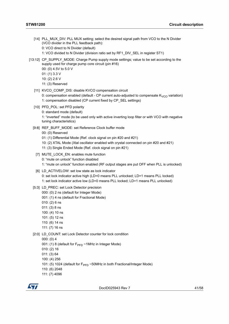
[14] PLL_MUX_DIV: PLL MUX setting; select the desired signal path from VCO to the N Divider (VCO divider in the PLL feedback path):
0: VCO direct to N Divider (default)
1: VCO divided to N Divider (division ratio set by RF1_DIV_SEL in register ST1)
[13:12] CP_SUPPLY_MODE: Charge Pump supply mode settings; value to be set according to the supply used for charge pump core circuit (pin #16)
00: (0) 4.5V to 5.0 V
01: (1) 3.3 V
10: (2) 2.6 V
11: (3) Reserved
[11] KVCO_COMP_DIS: disable KVCO compensation circuit
0: compensation enabled (default - CP current auto-adjusted to compensate KVCO variation)
1: compensation disabled (CP current fixed by CP_SEL settings)
[10] PFD_POL: set PFD polarity
0: standard mode (default)
1: “inverted” mode (to be used only with active inverting loop filter or with VCO with negative tuning characteristics)
[9:8] REF_BUFF_MODE: set Reference Clock buffer mode
00: (0) Reserved
01: (1) Differential Mode (Ref. clock signal on pin #20 and #21)
10: (2) XTAL Mode (Xtal oscillator enabled with crystal connected on pin #20 and #21)
11: (3) Single Ended Mode (Ref. clock signal on pin #21)
[7] MUTE_LOCK_EN: enables mute function
0: “mute on unlock” function disabled
1: “mute on unlock” function enabled (RF output stages are put OFF when PLL is unlocked)
[6] LD_ACTIVELOW: set low state as lock indicator
0: set lock indicator active high (LD=0 means PLL unlocked; LD=1 means PLL locked)
1: set lock indicator active low (LD=0 means PLL locked; LD=1 means PLL unlocked)
[5:3] LD_PREC: set Lock Detector precision
000: (0) 2 ns (default for Integer Mode)
001: (1) 4 ns (default for Fractional Mode)
010: (2) 6 ns
011: (3) 8 ns
100: (4) 10 ns
101: (5) 12 ns
110: (6) 14 ns
111: (7) 16 ns
[2:0] LD_COUNT: set Lock Detector counter for lock condition
000: (0) 4
001: (1) 8 (default for FPFD ~1MHz in Integer Mode)
010: (2) 16
011: (3) 64
100: (4) 256
101: (5) 1024 (default for FPFD ~50MHz in both Fractional/Integer Mode)
110: (6) 2048
111: (7) 4096
Circuit description STW81200
42/58 DocID025943 Rev 7
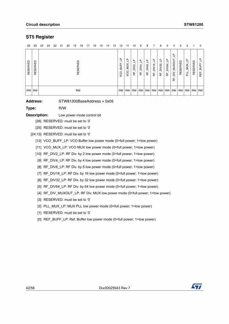
ST5 Register
Address: STW81200BaseAddress + 0x05
Type: R/W
Description: Low power mode control bit
26 25 24 23 22 21 20 19 18 17 16 15 14 13 12 11 10 9 8 7 6 5 4 3 2 1 0
RE
SE
RV
ED
RE
SE
RV
ED
RE
SE
RV
ED
VC
O_
BU
FF
_LP
VC
O_M
UX
_L
P
RF
_D
IV
2_L
P
RF
_D
IV
4_L
P
RF
_D
IV
8_L
P
RF
_D
IV
16
_L
P
RF
_D
IV
32
_L
P
RF
_D
IV
64
_L
P
RF
_D
IV
_M
UX
OU
T_
LP
RE
SE
RV
ED
PLL
_M
UX
_L
P
RE
SE
RV
ED
RE
F_
BU
FF
_L
P
RW RW RW RW RW RW RW RW RW RW RW RW RW RW RW RW
[26] RESERVED: must be set to ‘0’
[25] RESERVED: must be set to ‘0’
[24:13] RESERVED: must be set to ‘0’
[12] VCO_BUFF_LP: VCO Buffer low power mode (0=full power; 1=low power)
[11] VCO_MUX_LP: VCO MUX low power mode (0=full power; 1=low power)
[10] RF_DIV2_LP: RF Div. by 2 low power mode (0=full power; 1=low power)
[9] RF_DIV4_LP: RF Div. by 4 low power mode (0=full power; 1=low power)
[8] RF_DIV8_LP: RF Div. by 8 low power mode (0=full power; 1=low power)
[7] RF_DIV16_LP: RF Div. by 16 low power mode (0=full power; 1=low power)
[6] RF_DIV32_LP: RF Div. by 32 low power mode (0=full power; 1=low power)
[5] RF_DIV64_LP: RF Div. by 64 low power mode (0=full power; 1=low power)
[4] RF_DIV_MUXOUT_LP: RF Div. MUX low power mode (0=full power; 1=low power)
[3] RESERVED: must be set to ‘0’
[2] PLL_MUX_LP: MUX PLL low power mode (0=full power; 1=low power)
[1] RESERVED: must be set to ‘0’
[0] REF_BUFF_LP: Ref. Buffer low power mode (0=full power; 1=low power)
DocID025943 Rev 7 43/58
STW81200 Circuit description
57
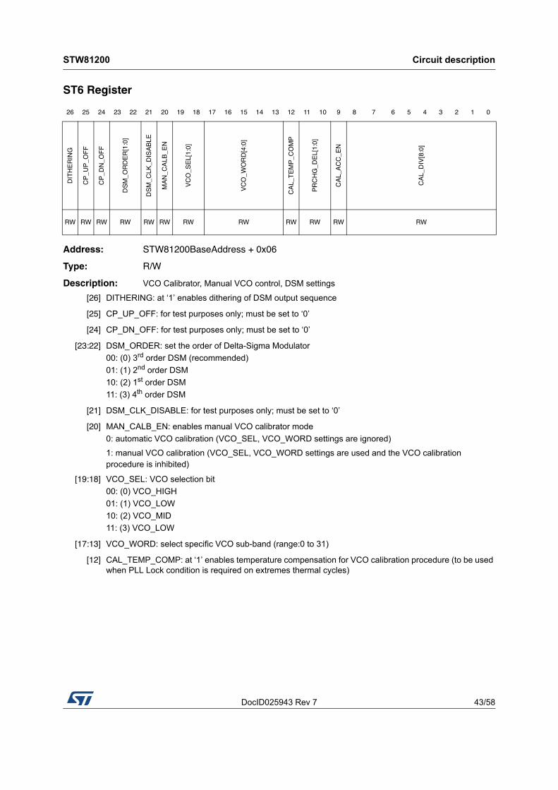
ST6 Register
Address: STW81200BaseAddress + 0x06
Type: R/W
Description: VCO Calibrator, Manual VCO control, DSM settings
26 25 24 23 22 21 20 19 18 17 16 15 14 13 12 11 10 9 8 7 6 5 4 3 2 1 0
DIT
HE
RIN
G
CP
_U
P_
OF
F
CP
_D
N_
OF
F
DS
M_
OR
DE
R[1
:0
]
DS
M_
CL
K_D
IS
AB
LE
MA
N_C
AL
B_E
N
VC
O_
SE
L[1:0
]
VC
O_
WO
RD
[4
:0
]
CA
L_
TE
MP
_C
OM
P
PR
CH
G_
DE
L[1
:0
]
CA
L_A
CC
_E
N
CA
L_
DIV
[8:0
]
RW RW RW RW RW RW RW RW RW RW RW RW
[26] DITHERING: at ‘1’ enables dithering of DSM output sequence
[25] CP_UP_OFF: for test purposes only; must be set to ‘0’
[24] CP_DN_OFF: for test purposes only; must be set to ‘0’
[23:22] DSM_ORDER: set the order of Delta-Sigma Modulator
00: (0) 3rd order DSM (recommended)
01: (1) 2nd order DSM
10: (2) 1st order DSM
11: (3) 4th order DSM
[21] DSM_CLK_DISABLE: for test purposes only; must be set to ‘0’
[20] MAN_CALB_EN: enables manual VCO calibrator mode
0: automatic VCO calibration (VCO_SEL, VCO_WORD settings are ignored)
1: manual VCO calibration (VCO_SEL, VCO_WORD settings are used and the VCO calibration procedure is inhibited)
[19:18] VCO_SEL: VCO selection bit
00: (0) VCO_HIGH
01: (1) VCO_LOW
10: (2) VCO_MID
11: (3) VCO_LOW
[17:13] VCO_WORD: select specific VCO sub-band (range:0 to 31)
[12] CAL_TEMP_COMP: at ‘1’ enables temperature compensation for VCO calibration procedure (to be used when PLL Lock condition is required on extremes thermal cycles)

Circuit description STW81200
44/58 DocID025943 Rev 7
[11:10] PRCHG_DEL: set the number of calibration slots for pre-charge of VCTRL node at the Voltage reference value used during VCO calibration procedure
00: (0) 1 slot (default)
01: (1) 2 slots
10: (2) 3 slots
11: (3) 4 slots
[9] CAL_ACC_EN: at ‘1’ increase calibrator accuracy by removing residual error taking 2 additional calibration slots (default = ‘0’)
[8:0] CAL_DIV: Set Calibrator Clock divider ratio (Range:1 to 511); ‘0’ set the maximum ratio (‘511’)

DocID025943 Rev 7 45/58
STW81200 Circuit description
57
ST7 Register
Address: STW81200BaseAddress + 0x07
Type: R/W
Description: Fast Lock control, LD_SDO settings
26 25 24 23 22 21 20 19 18 17 16 15 14 13 12 11 10 9 8 7 6 5 4 3 2 1 0
RE
SE
RV
ED
LD
_S
DO
_tris
ta
te
LD
_S
DO
_M
OD
E
SP
I_D
ATA
_O
UT
_D
IS
AB
LE
LD
_S
DO
_S
EL
[1
:0
]
RE
GD
IG
_O
CP
_D
IS
CY
CL
E_
SL
IP
_E
N
FS
TL
CK
_E
N
CP
_S
EL
_F
L[4
:0
]
FS
TLC
K_
CN
T[12
:0]
RW RW RW RW RW RW RW RW RW RW
[26] RESERVED: must be set to ‘0’
[25] LD_SDO_tristate: at ‘1’ put LD_SDO out pin in Tri-State mode
[24] LD_SDO_MODE: LD_SDO output interface mode selection
0: Open Drain mode (Level Range: 1.8V to 3.6V)
1: 2.5V CMOS output mode
[23] SPI_DATA_OUT_DISABLE: disable auto-switch of LD_SDO pin during SPI read mode
0: LD_SDO pin automatically switched to SPI data out line during SPI read mode
1: LD_SDO pin fixed to Lock detector indication (SPI read operation not possible)
[22:21] LD_SDO_SEL: LD_SDO Mux output selection bit
00: (0) Lock Detector (default)
01: (1) VCO Divider output (for test purposes only)
10: (2) Calibrator VCO Divider output (for test purposes only)
11: (3) Fast Lock clock output (for test purposes only)
[20] REGDIG_OCP_DIS: for test purposes only ; must be set to ‘0’ (at ‘1’ disable the over-current protection of Digital LDO Voltage Regulator)
[19] CYCLE_SLIP_EN: at ‘1’ enables Cycle Slip feature
[18] FSTLCK_EN: at ‘1’ enables Fast lock mode using pin #6 (PD_RF2/FL_SW)
[17:13] CP_SEL_FL: set the Charge Pump current during fast lock time slot (range:0 to 31)
[12:0] FSTLCK_CNT: Fast-Lock counter value (Range: 2 to 8191); set duration of fast-lock time slot as number of FPFD cycles

Circuit description STW81200
46/58 DocID025943 Rev 7
ST8 Register
Address: STW81200BaseAddress + 0x08
Type: R/W
Description: LDO Voltage Regulator settings
26 25 24 23 22 21 20 19 18 17 16 15 14 13 12 11 10 9 8 7 6 5 4 3 2 1 0
PD
_R
F2
_D
IS
AB
LE
RE
SE
RV
ED
RE
SE
RV
ED
RE
SE
RV
ED
RE
SE
RV
ED
RE
SE
RV
ED
RE
SE
RV
ED
RE
G_
OC
P_
DIS
RE
G_
DIG
_P
D
RE
G_D
IG
_V
OU
T[1
:0
]
RE
SE
RV
ED
RE
G_
RE
F_P
D
RE
G_R
EF
_V
OU
T[1
:0
]
RE
SE
RV
ED
RE
G_
RF
_P
D
RE
G_R
F_V
OU
T[1
:0
]
RE
SE
RV
ED
RE
G_
VC
O_
PD
RE
G_
VC
O_
VO
UT
[1
:0
]
RE
SE
RV
ED
RE
G_
VC
O_
4V
5_
PD
RE
G_
VC
O_
4V
5_
VO
UT
[1
:0
]
RW RW RW RW RW RW RW RW RW RW RW RW RW RW RW RW RW RW RW RW RW RW
[26] PD_RF2_DISABLE: at ‘1’ disable the hardware power down function of the pin PD_RF2 (pin #6) thus allowing the pin PD_RF1 (pin #5) to control the power down status of both RF Output stages
[25] RESERVED: must be set to ‘0’
[24] RESERVED: must be set to ‘0’
[23] RESERVED: must be set to ‘0’
[22] RESERVED: must be set to ‘0’
[21] RESERVED: must be set to ‘0’
[20] RESERVED: must be set to ‘0’
[19] REG_OCP_DIS: for test purposes only; must be set to ‘0’ (at ‘1’ disable the over-current protection of LDO Voltage Regulators except DIG regulator)
[18] REG_DIG_PD: DIGITAL Regulator power down; must be set to ‘0’
[17:16] REG_DIG_VOUT: DIGITAL Regulator output voltage set
00: (0) 2.6 V (Default)
01: (1) 2.3 V (for test purposes only)
10: (2) 2.4 V (for test purposes only)
11: (3) 2.5 V (for test purposes only)
[15] RESERVED: must be set to ‘0’
[14] REG_REF_PD: REFERENCE CLOCK Regulator power down; must be set to ‘0’
[13:12] REG_REF_VOUT: REFERENCE CLOCK Regulator output voltage set
00: (0) 2.6 V (default)
01: (1) 2.5 V (for test purposes only)
10: (2) 2.7 V (for test purposes only)
11: (3) 2.8 V (for test purposes only)
[11] RESERVED: must be set to ‘0’
[10] REG_RF_PD: RF Output section Regulator power down; must be set to ‘0’

DocID025943 Rev 7 47/58
STW81200 Circuit description
57
ST9 Register
Address: STW81200BaseAddress + 0x09
Type: R/W
Description: Reserved (Test & Initialization bit)
[9:8] REG_RF_VOUT: RF Output section Regulator output voltage set
00: (0) 2.6 V (default)
01: (1) 2.5 V (for test purposes only)
10: (2) 2.7 V (for test purposes only)
11: (3) 2.8 V (for test purposes only)
[7] RESERVED: must be set to ‘0’
[6] REG_VCO_PD: VCO bias-and-control regulator power down; must be set to ‘0’
[5:4] REG_VCO_VOUT: VCO bias-and-control regulator output voltage set
00: (0) 2.6 V (default)
01: (1) 2.5 V (for test purposes only)
10: (2) 2.7 V (for test purposes only)
11: (3) 2.8 V (for test purposes only)
[3] RESERVED: must be set to ‘0’
[2] REG_VCO_4V5_PD: High-voltage regulator power down (to be used to supply VCO core, RF output final stage and Charge Pump). Must be set to ‘0’
[1:0] REG_VCO_4V5_VOUT: High-voltage regulator output voltage set (to be used to supply VCO core, RF output final stage and charge-pump output)
00: (0) 5.0 V (Require 5.4 V unregulated voltage line on pin# 36 for test purposes only)
01: (1) 2.6 V (3.0-5.4 V unregulated voltage line Range allowed on pin#36)
10: (2) 3.3 V (3.6-5.4 V unregulated voltage line Range allowed on pin#36)
11: (3) 4.5 V (5.0-5.4 V unregulated voltage line Range allowed on pin#36)
26 25 24 23 22 21 20 19 18 17 16 15 14 13 12 11 10 9 8 7 6 5 4 3 2 1 0
RE
SE
RV
ED
RW
[26:0] RESERVED: Test & Initialization bit; must be set to ‘0’
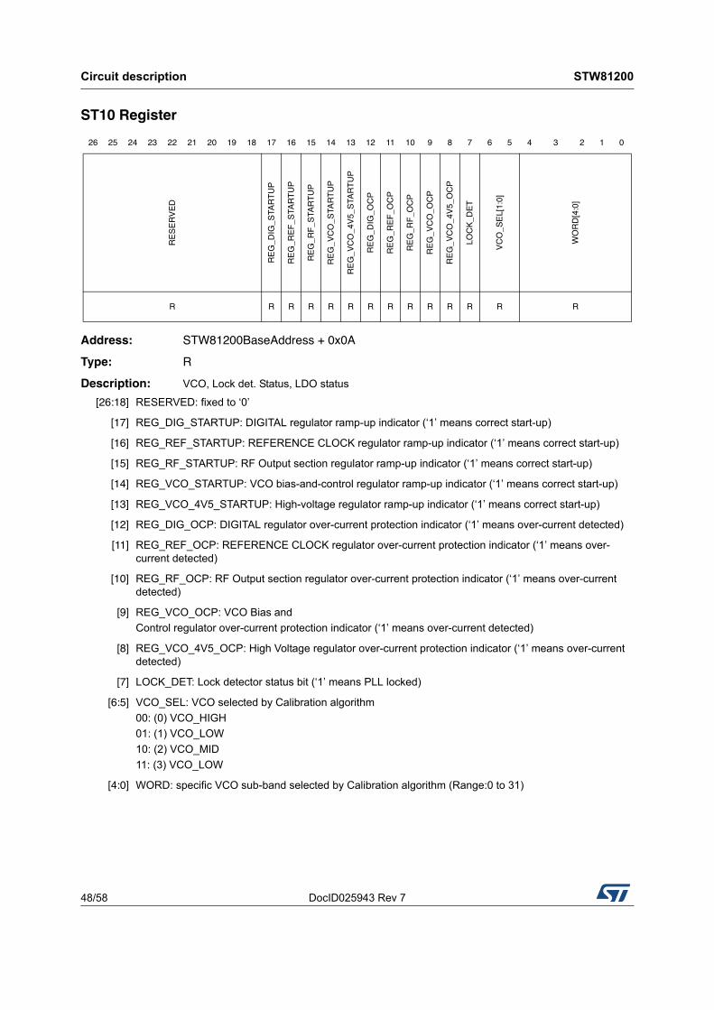
Circuit description STW81200
48/58 DocID025943 Rev 7
ST10 Register
Address: STW81200BaseAddress + 0x0A
Type: R
Description: VCO, Lock det. Status, LDO status
26 25 24 23 22 21 20 19 18 17 16 15 14 13 12 11 10 9 8 7 6 5 4 3 2 1 0
RE
SE
RV
ED
RE
G_
DIG
_S
TA
RT
UP
RE
G_R
EF
_S
TA
RT
UP
RE
G_
RF
_S
TA
RT
UP
RE
G_
VC
O_
STA
RT
UP
RE
G_
VC
O_
4V
5_
STA
RT
UP
RE
G_D
IG
_O
CP
RE
G_
RE
F_
OC
P
RE
G_R
F_O
CP
RE
G_
VC
O_
OC
P
RE
G_
VC
O_
4V
5_
OC
P
LO
CK
_D
ET
VC
O_
SE
L[1:0
]
WO
RD
[4
:0]
R R R R R R R R R R R R R R
[26:18] RESERVED: fixed to ‘0’
[17] REG_DIG_STARTUP: DIGITAL regulator ramp-up indicator (‘1’ means correct start-up)
[16] REG_REF_STARTUP: REFERENCE CLOCK regulator ramp-up indicator (‘1’ means correct start-up)
[15] REG_RF_STARTUP: RF Output section regulator ramp-up indicator (‘1’ means correct start-up)
[14] REG_VCO_STARTUP: VCO bias-and-control regulator ramp-up indicator (‘1’ means correct start-up)
[13] REG_VCO_4V5_STARTUP: High-voltage regulator ramp-up indicator (‘1’ means correct start-up)
[12] REG_DIG_OCP: DIGITAL regulator over-current protection indicator (‘1’ means over-current detected)
[11] REG_REF_OCP: REFERENCE CLOCK regulator over-current protection indicator (‘1’ means over-current detected)
[10] REG_RF_OCP: RF Output section regulator over-current protection indicator (‘1’ means over-current detected)
[9] REG_VCO_OCP: VCO Bias and
Control regulator over-current protection indicator (‘1’ means over-current detected)
[8] REG_VCO_4V5_OCP: High Voltage regulator over-current protection indicator (‘1’ means over-current detected)
[7] LOCK_DET: Lock detector status bit (‘1’ means PLL locked)
[6:5] VCO_SEL: VCO selected by Calibration algorithm
00: (0) VCO_HIGH
01: (1) VCO_LOW
10: (2) VCO_MID
11: (3) VCO_LOW
[4:0] WORD: specific VCO sub-band selected by Calibration algorithm (Range:0 to 31)

DocID025943 Rev 7 49/58
STW81200 Circuit description
57
ST11 Register
Address: STW81200BaseAddress + 0x0B
Type: R
Description: Device ID
26 25 24 23 22 21 20 19 18 17 16 15 14 13 12 11 10 9 8 7 6 5 4 3 2 1 0
Dev
ice
_ID
R
[26:0] Device_ID: Device Identifier (0x0008021)

Circuit description STW81200
50/58 DocID025943 Rev 7
7.16 Power ON sequence
In order to guarantee the correct start-up of the internal circuitry after the power on, the following steps must be followed:
1. Power up the device (LDO supply pins: pin#9 #18, #28 and #36)
2. Once the voltages applied on the LDO supply pins are stable, wait 50 ms. (After this transient time, the LDOs are powered on with the regulated voltages available at pins #2, #8, #19, #27 and #29, while all other circuits are in power down mode)
3. Provide the reference clock signal
4. Implement the first programming sequence as follows:
a) Program register ST9 (test and initialization) with all bit set to ‘0’
b) Program register ST0 according to the desired configuration
c) Program the following registers in the specified order according to the desired configuration: ST8, ST7, ST6, ST5, ST4, ST3, ST2, ST1, ST0
5. Check the PLL Lock status on pin LD_SDO (pin #26) and/or read all relevant information provided on registers ST10 and ST11.
7.17 Example of Register programming
Setup conditions and requirements:
• Unregulated Supply voltage: 5.0 V
• Reference Clock: 122.88 MHz, single-ended, sine wave
• LO Frequency: 2646.96 MHz – exact freq. mode (VCO Frequency=5293.92 MHz)
• Output Power: +7 dBm (differential)
• Phase Noise requirements: full performance VCO, full performance Noise floor.
Register configurations (Hex values including register address)
• ST9 = 0x48000000 (initialization; all bits set to ‘0’)
• ST8 = 0x40000003 (REG_4V5 = 4.5 V)
• ST7 = 0x39000000 (“fast lock” not used; LD_SDO pin configured as 2.5 V CMOS buffer)
• ST6 = 0x30001000 (DITHERING=0; DSM_ORDER=0 for 3rd order DSM; CAL_TEMP_COMP=1 to guarantee lock on extreme temperature drift)
• ST5 = 0x28000000 (low power modes not used)
• ST4 = 0x2387838D (lock detector setting for fractional mode and FPFD = 61.44 MHz; REF_BUF_MODE=3 for single-ended mode; VCO_AMP=15 for best VCO phase noise @4.5 V supply; RF_OUT_PWR=7 to have +7 dBm differential)
• ST3 = 0x18008002 (PFD_DEL_MODE = ‘VCO_DIV_delayed’, R=2 and REF_PATH_SEL = 0 ‘direct’ for FPFD= 61.44 MHz)
• ST2 = 0x13000080 (MOD=128; RF2_OUT_PD=1 for RF2 Output in power down)
• ST1 = 0x08200015 (FRAC=21; RF1_DIVSEL=1 set RF1 Output with VCO freq. Divided By 2)
• ST0 = 0x03E00056 (NINT=86; PFD_DEL = 1.2 ns; CPSEL = 31 for Icp = 4.9 mA)

DocID025943 Rev 7 51/58
STW81200 Application information
57
8 Application information
8.1 Application diagrams
Figure 33. Application diagram (internal VCO)
Note: This diagram shows a simplified schematic; the Evaluation Board schematic should be used as reference for connections and components values. Visit the STW81200 product page on the ST website www.st.com/stw81200ad to download the Evaluation Board Data Brief including PCB schematics.

Application information STW81200
52/58 DocID025943 Rev 7
Figure 34. Application diagram (external VCO)
Note: This diagram shows a simplified schematic; the Evaluation Board schematic should be used as reference for connections and components values. Visit the STW81200 product page on the ST website www.st.com/stw81200ad to download the evaluation board data brief including PCB schematics.

DocID025943 Rev 7 53/58
STW81200 Application information
57
8.2 Thermal PCB design considerations
The STW81200 QFN package offers a low thermal resistance (θJC ~3°C/W on a JEDEC Multi-Layer Board). Preferred thermal flow in QFN package is through the bottom central pad.
The central thermal pad provides a solderable surface on the top of the PCB (for soldering the package die paddle on the board). Thermal vias are needed to provide a thermal path to the inner and bottom layers of the PCB in order to remove/dissipate the heat. The size of the thermal pad can be matched with the exposed die paddle, or it may be smaller taking into consideration clearance for vias to route the inner row signals.
A PCB can be designed to achieve a thermal impedance of 2 to 4°C/W through a 1.6 mm (.063”) thick FR-4 type PCB (a reliable, low cost solution).
For example the ST EVAL KIT uses a 0.8 mm thick PCB with a thermal impedance of ~50°C/W for a single via filled with solder. 25 vias are used, giving a thermal impedance of ~2°C/W with solder-filled vias (50°C/W divided by 25 vias).
Using a plate on the underside of the PCB (a common solution in STW81200 applications, as the plate is typically the metal housing of the application assembly) brings the total thermal resistance (junction to housing in the customer application) below 10°C/W.
As the typical power dissipation of the STW81200 is approximately 1.5 W, at maximum specified ambient temperature (85°C) a junction temperature of less than 100°C is attainable. This is well below the maximum specified value (125°C) to ensure safe operation of the STW81200 in worst-temperature conditions.
The ST EVAL KIT is not provided with additional heatsinking, and the thermal resistance (θJA) measured in the EVAL BOARD is ~30°C/W.
Evaluation Kit STW81200
54/58 DocID025943 Rev 7
9 Evaluation Kit
An evaluation kit can be supplied upon request (Order Code: STW81200-EVB), including the following:
• Evaluation board
• GUI (graphical user interface) to configure the board and the STW81200 IC
• STWPLLSim software for PLL loop filter design and phase noise/transient simulation
• A comprehensive set of documentation (Evaluation board data brief including PCB
schematics and GUI help, STWPLLSim User Manual).
The evaluation kit and the related SW and documentation can be ordered/downloaded from the ST website at the followng address: www.st.com/stw81200ad.
Table 12. STW81200 order codes
Order Code Description
STW81200-EVB STW81200 Evaluation Kit (Evaluation Board, GUI and STWPLLSim tool)
STSW-RFSOL001 STWPLLSim simulation tool for STW81200
STSW-RFSOL002 GUI for configuring STW81200 evaluation board
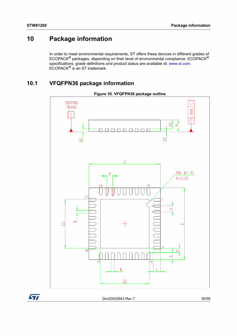
DocID025943 Rev 7 55/58
STW81200 Package information
57
10 Package information
In order to meet environmental requirements, ST offers these devices in different grades of ECOPACK® packages, depending on their level of environmental compliance. ECOPACK® specifications, grade definitions and product status are available at: www.st.com. ECOPACK® is an ST trademark.
10.1 VFQFPN36 package information
Figure 35. VFQFPN36 package outline
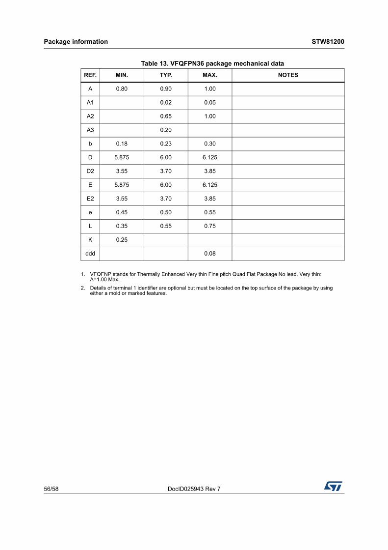
Package information STW81200
56/58 DocID025943 Rev 7
1. VFQFNP stands for Thermally Enhanced Very thin Fine pitch Quad Flat Package No lead. Very thin: A=1.00 Max.
2. Details of terminal 1 identifier are optional but must be located on the top surface of the package by using either a mold or marked features.
Table 13. VFQFPN36 package mechanical data
REF. MIN. TYP. MAX. NOTES
A 0.80 0.90 1.00
A1 0.02 0.05
A2 0.65 1.00
A3 0.20
b 0.18 0.23 0.30
D 5.875 6.00 6.125
D2 3.55 3.70 3.85
E 5.875 6.00 6.125
E2 3.55 3.70 3.85
e 0.45 0.50 0.55
L 0.35 0.55 0.75
K 0.25
ddd 0.08

DocID025943 Rev 7 57/58
STW81200 Revision history
57
11 Revision history
Table 14. Document revision history
Date Revision Changes
21-Feb-2014 1 Initial release.
07-Apr-2014 2 Removed confidential banner
04-Sep-2014 3
Added HBM footnote in Table 3: Absolute maximum ratings
Updated device ID in ST11 Register on page 49
Updated to use latest corporate template and legal disclaimer.
23-Sep-2014 4 Changed ‘Multi-band’ to ‘Wideband’ in document title.
12-Jun-2015 5
Renamed pin 14 to VDD_CP in Table 2: Pin description.
Added IOL and IOH values in Table 5: Digital logic levels
Updated parameter VICP in Table 6: Electrical specifications
Updated Figure 9 through Figure 28
Added Section 7.3.1: Fractional spurs and compensation mechanism.
Updated
– Section 7.6: Charge pump.
– Section 7.9: Voltage controlled oscillators (VCOs)
– Section 7.10: RF output divider stage
– Section 7.11: Low-power functional modes
– Section 7.12: LDO voltage regulators
Updated ST0 register description in Table 11: SPI Register map (address 12 to 15 not available)
Updated following register bitfield descriptions:
– STW81200 register descriptions bit PFD_DEL
– ST3 Register bits CP_LEAK and DNSPLIT_EN
– ST4 Register bit RF_OUT_PWR
– ST6 Register bit MAN_CALB_EN
– ST8 Register bit REG_VCO_4V5_VOUT
– ST10 Register bit REG_VCO_OCP
Updated Section 7.17: Example of Register programming
Added notes to Figure 33 and Figure 34
Added Section 9: Evaluation Kit
Re formatted Section 10: Package information to comply with latest corporate guidelines.
08-Jul-2015 6 Regenerated for XML generation.
04-Jan-2016 7
Updated parameter Kvco in Table 6: Electrical specifications
Updated:
– Section 7.6: Charge pump
– Section 7.16: Power ON sequence.
Re-named Section 8: Application information, and added Section 8.2: Thermal PCB design considerations.
In Table 6: Electrical specifications updated dimensions D2 and E2.

STW81200
58/58 DocID025943 Rev 7
IMPORTANT NOTICE – PLEASE READ CAREFULLY
STMicroelectronics NV and its subsidiaries (“ST”) reserve the right to make changes, corrections, enhancements, modifications, and improvements to ST products and/or to this document at any time without notice. Purchasers should obtain the latest relevant information on ST products before placing orders. ST products are sold pursuant to ST’s terms and conditions of sale in place at the time of order acknowledgement.
Purchasers are solely responsible for the choice, selection, and use of ST products and ST assumes no liability for application assistance or the design of Purchasers’ products.
No license, express or implied, to any intellectual property right is granted by ST herein.
Resale of ST products with provisions different from the information set forth herein shall void any warranty granted by ST for such product.
ST and the ST logo are trademarks of ST. All other product or service names are the property of their respective owners.
Information in this document supersedes and replaces information previously supplied in any prior versions of this document.
© 2016 STMicroelectronics – All rights reserved


