Week 8 The 8088 and 8086 Microprocessorsalkar/ELE336/ele336_2014_week8.pdf · 8086 and 8088...
48
Week 8 The 8088 and 8086 Microprocessors
Transcript of Week 8 The 8088 and 8086 Microprocessorsalkar/ELE336/ele336_2014_week8.pdf · 8086 and 8088...
Week 8
The 8088 and 8086 Microprocessors
2
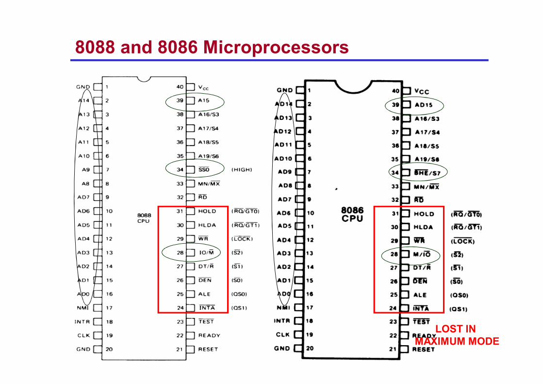
8086 and 8088 Microprocessors
• 8086 announced in 1978; 8086 is a 16 bit microprocessor with a 16 bit data bus
• 8088 announced in 1979; 8088 is a 16 bit microprocessor with an 8 bit data bus
• Both manufactured using High-performance Metal Oxide Semiconductor (HMOS) technology
• Both contain about 29000 transistors• Both are packaged in 40 pin dual-in-line package (DIP)• Address lines A0-A7 and Data lines D0-D7 are multiplexed in
8088. These lines are labelled as AD0-AD7.– By multiplexed we mean that the same pysical pin carries an address
bit at one time and the data bit another time• Address lines A0-A15 and Data lines D0-D15 are multiplexed in
8086. These lines are labelled as AD0-AD15.
3
8088 and 8086 Microprocessors
LOST IN MAXIMUM MODE
4
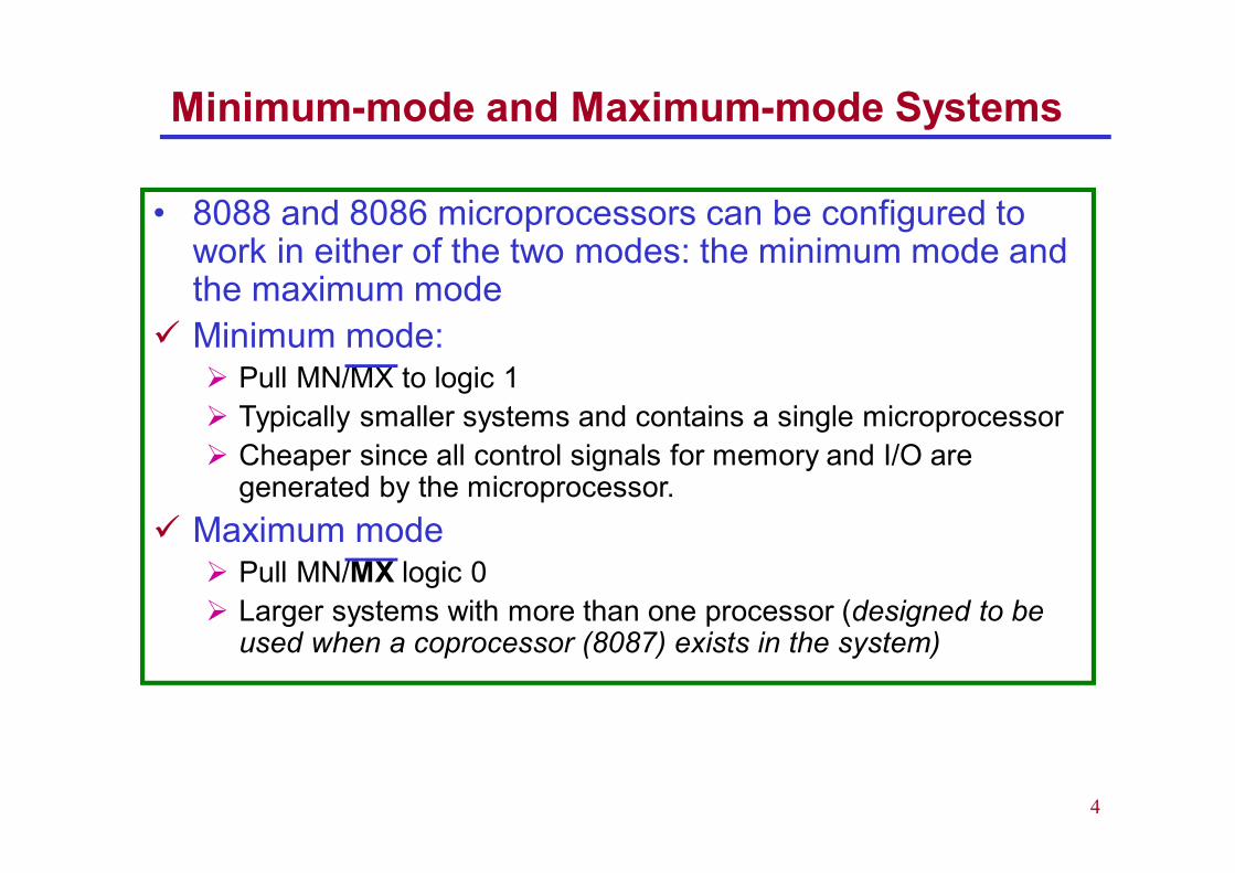
Minimum-mode and Maximum-mode Systems
• 8088 and 8086 microprocessors can be configured to work in either of the two modes: the minimum mode and the maximum mode
Minimum mode: Pull MN/MX to logic 1 Typically smaller systems and contains a single microprocessor Cheaper since all control signals for memory and I/O are
generated by the microprocessor. Maximum mode
Pull MN/MX logic 0 Larger systems with more than one processor (designed to be
used when a coprocessor (8087) exists in the system)

5
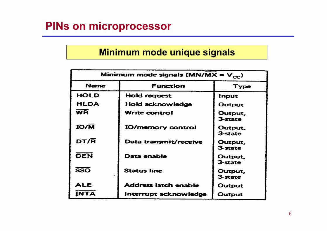
PINs on microprocessorSignals common to both minimum and maximum systems
6
PINs on microprocessor
Minimum mode unique signals
7
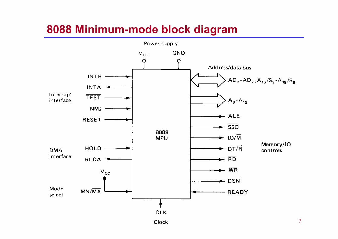
8088 Minimum-mode block diagram
8
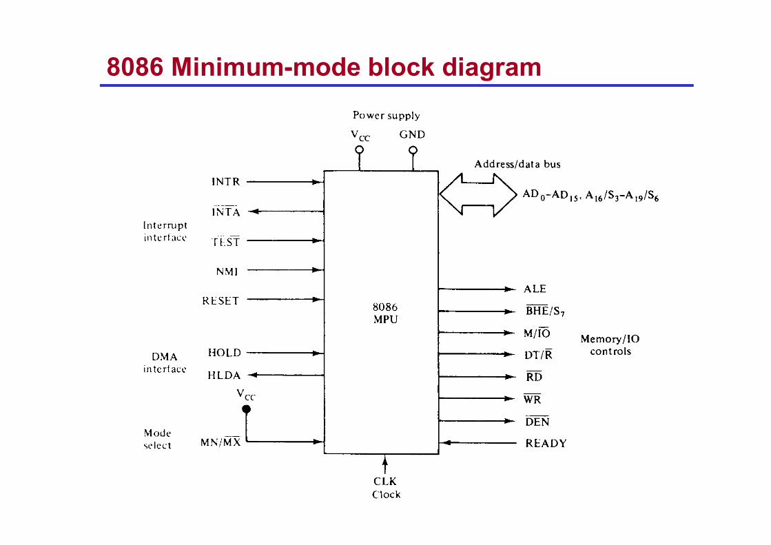
8086 Minimum-mode block diagram
9
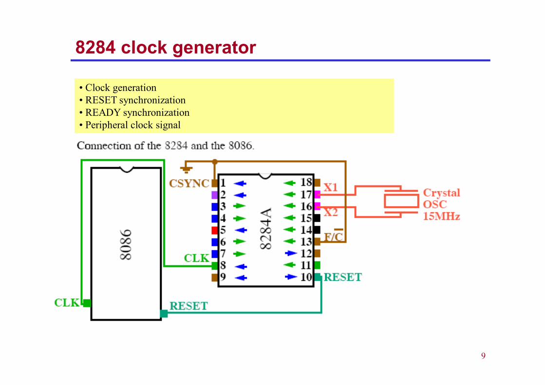
8284 clock generator
• Clock generation• RESET synchronization• READY synchronization• Peripheral clock signal
10
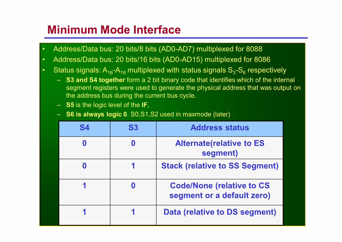
Minimum Mode Interface • Address/Data bus: 20 bits/8 bits (AD0-AD7) multiplexed for 8088• Address/Data bus: 20 bits/16 bits (AD0-AD15) multiplexed for 8086• Status signals: A16-A19 multiplexed with status signals S3-S6 respectively
– S3 and S4 together form a 2 bit binary code that identifies which of the internal segment registers were used to generate the physical address that was output on the address bus during the current bus cycle.
– S5 is the logic level of the IF, – S6 is always logic 0. S0,S1,S2 used in maxmode (later)
S4 S3 Address status
0 0 Alternate(relative to ES segment)
0 1 Stack (relative to SS Segment)
1 0 Code/None (relative to CS segment or a default zero)
1 1 Data (relative to DS segment)
11
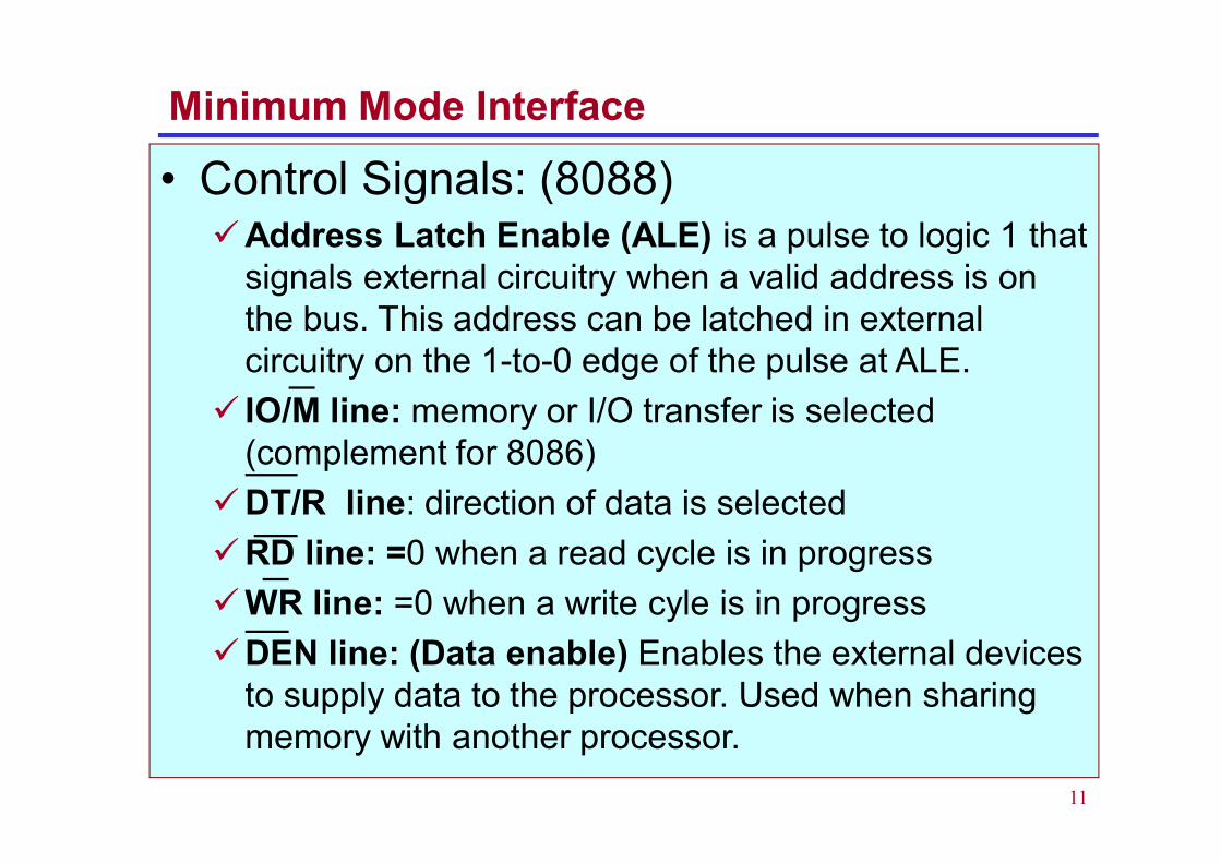
Minimum Mode Interface
• Control Signals: (8088) Address Latch Enable (ALE) is a pulse to logic 1 that
signals external circuitry when a valid address is on the bus. This address can be latched in external circuitry on the 1-to-0 edge of the pulse at ALE.
IO/M line: memory or I/O transfer is selected (complement for 8086)
DT/R line: direction of data is selectedRD line: =0 when a read cycle is in progressWR line: =0 when a write cyle is in progressDEN line: (Data enable) Enables the external devices
to supply data to the processor. Used when sharing memory with another processor.
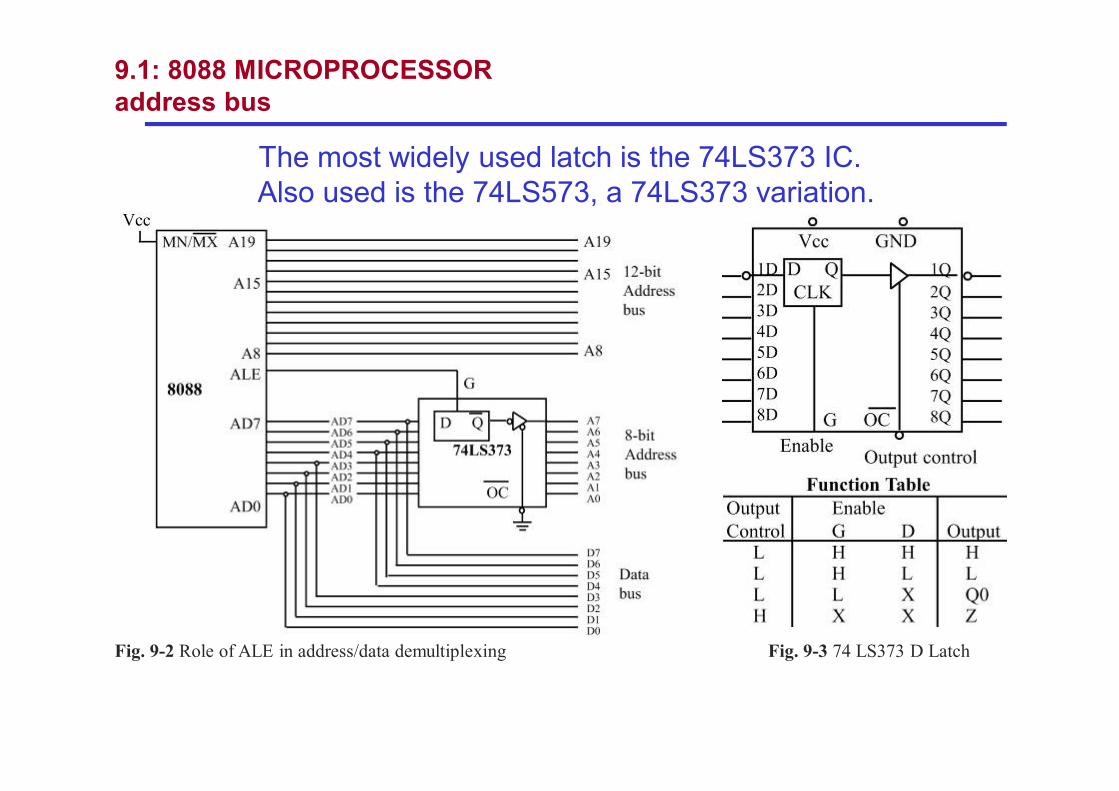
9.1: 8088 MICROPROCESSOR address bus
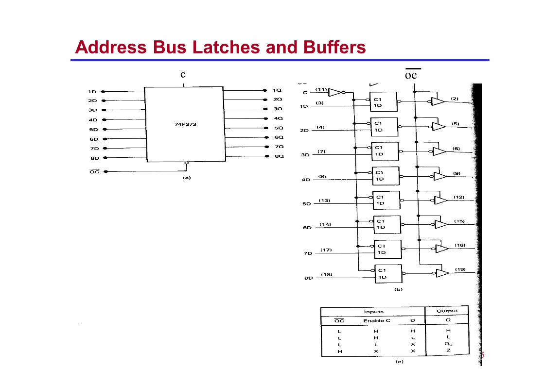
Fig. 9-2 Role of ALE in address/data demultiplexing Fig. 9-3 74 LS373 D Latch
The most widely used latch is the 74LS373 IC.Also used is the 74LS573, a 74LS373 variation.
13
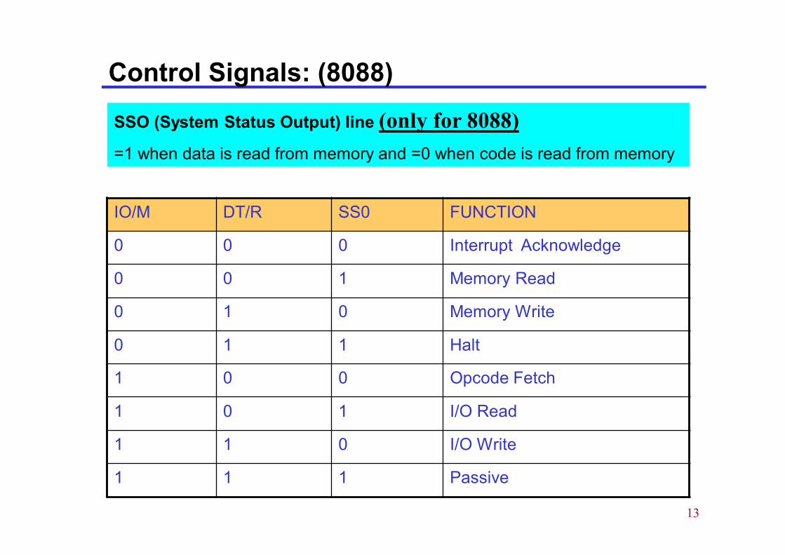
Control Signals: (8088)
SSO (System Status Output) line (only for 8088)=1 when data is read from memory and =0 when code is read from memory
IO/M DT/R SS0 FUNCTION
0 0 0 Interrupt Acknowledge
0 0 1 Memory Read
0 1 0 Memory Write
0 1 1 Halt
1 0 0 Opcode Fetch
1 0 1 I/O Read
1 1 0 I/O Write
1 1 1 Passive
14
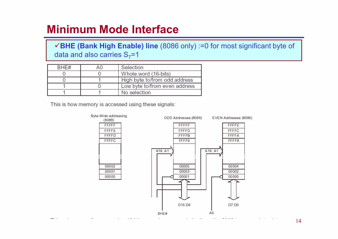
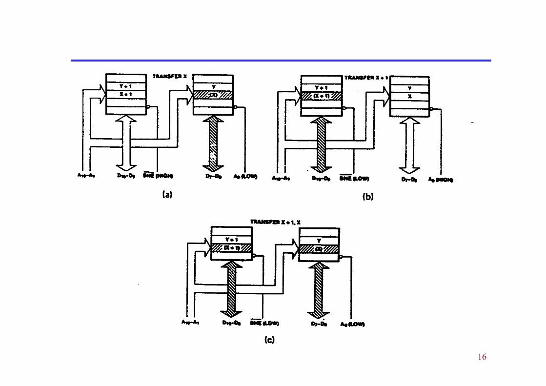
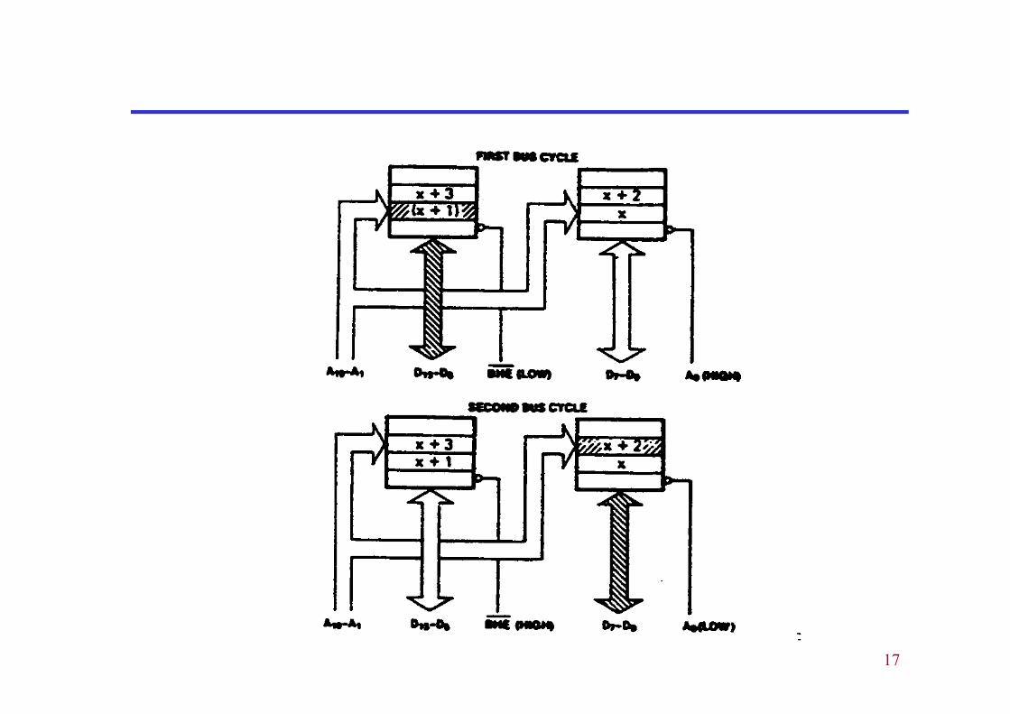
Minimum Mode InterfaceBHE (Bank High Enable) line (8086 only) :=0 for most significant byte of data and also carries S7=1

15
Data Transfer
16
17

18
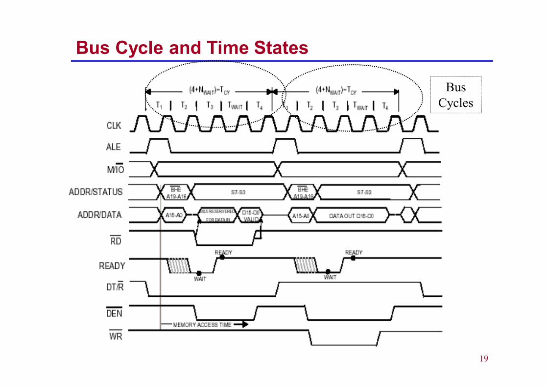
Bus Cycle and Time States
• A bus cycle (machine cycle) defines the basic operation that a microprocessor performs to communicate with external devices
• Examples of bus cycles are memory read, memory write, input/output read and input/output write.
• A bus cycle corresponds to a sequence of events that starts with an address being output on the system bus followed by a read or write data transfer
• During these operations, a series of control signals are also produced by the MPU to control the direction and timing of the bus.
• Each bus cycle consists of at least four clock periods: T1, T2, T3, and T4.
• These clock periods are also called the T-States
19
Bus Cycle and Time States
BusCycles

20
Bus Cycle and Time States
T1 - start of bus cycle. Actions include setting control signals (or S0-S2 status lines) to give the required values for ALE, DTR IO/M putting a valid address onto the address bus.
T2 - the RD or WR control signals are issued, DEN is asserted and in the case of a write, data is put onto the data bus. The DEN turns on the data bus buffers to connect the CPU to the external data bus. The READY input to the CPU is sampled at the end of T2 and if READY is low, a wait state TW (one or more) is inserted before T3 begins.
T3 - this clock period is provided to allow memory to access the data. If the bus cycle is a read cycle, the data bus is sampled at the end of T3.
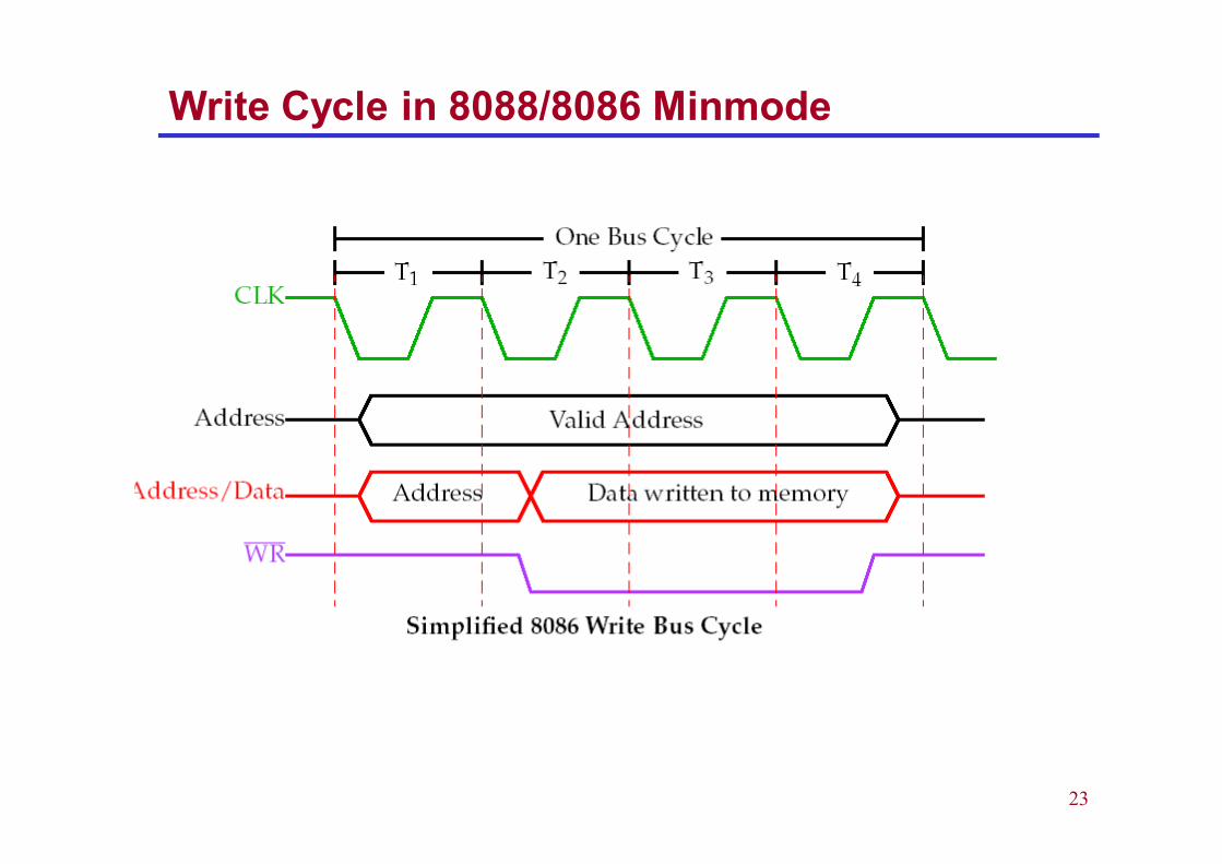
T4 - all bus signals are deactivated in preparation for the next clock cycle. The 8088 also finishes sampling the data (in a read cycle) in this period. For the write cycle, the trailing edge of the WR signal transfers data to the memory or I/O, which activates and write when WR returns to logic 1 level.
21
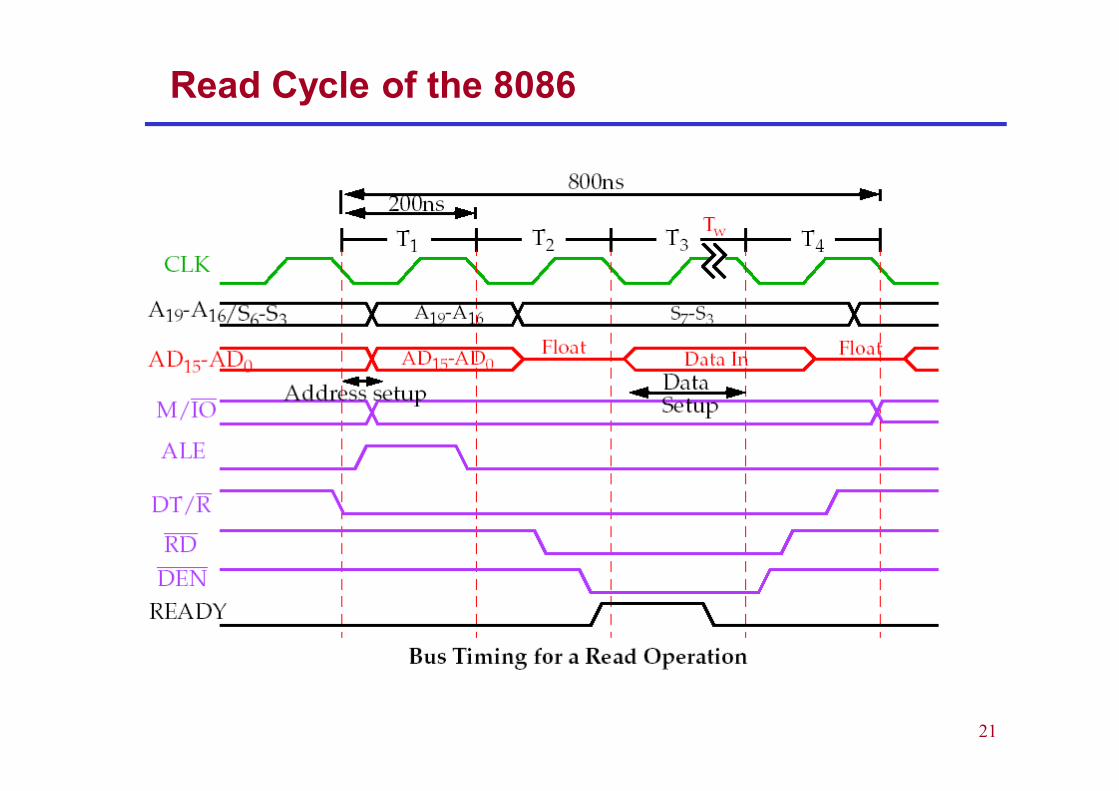
Read Cycle of the 8086
22
Read Cycle
• Each BUS CYCLE (machine cycle) on the 8086 equals four system clocking periods (T states).
• The clock rate is 5MHz, therefore one Bus Cycle is 800ns.• Memory specs (memory access time) must match constraints of
system timing.• For example, bus timing for a read operation shows almost 600ns
are needed to read data.• However, memory must access faster due to setup times, e.g.• Address setup and data setup.• This subtracts off about 150ns.• Therefore, memory must access in at least 450ns minus another 30-
40ns guard band for buffers and decoders.• 420ns DRAM required for the 8086.
23
Write Cycle in 8088/8086 Minmode
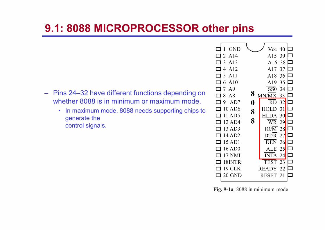
9.1: 8088 MICROPROCESSOR other pins
– Pins 24–32 have different functions depending on whether 8088 is in minimum or maximum mode.
• In maximum mode, 8088 needs supporting chips to generate thecontrol signals.
Fig. 9-1a 8088 in minimum mode
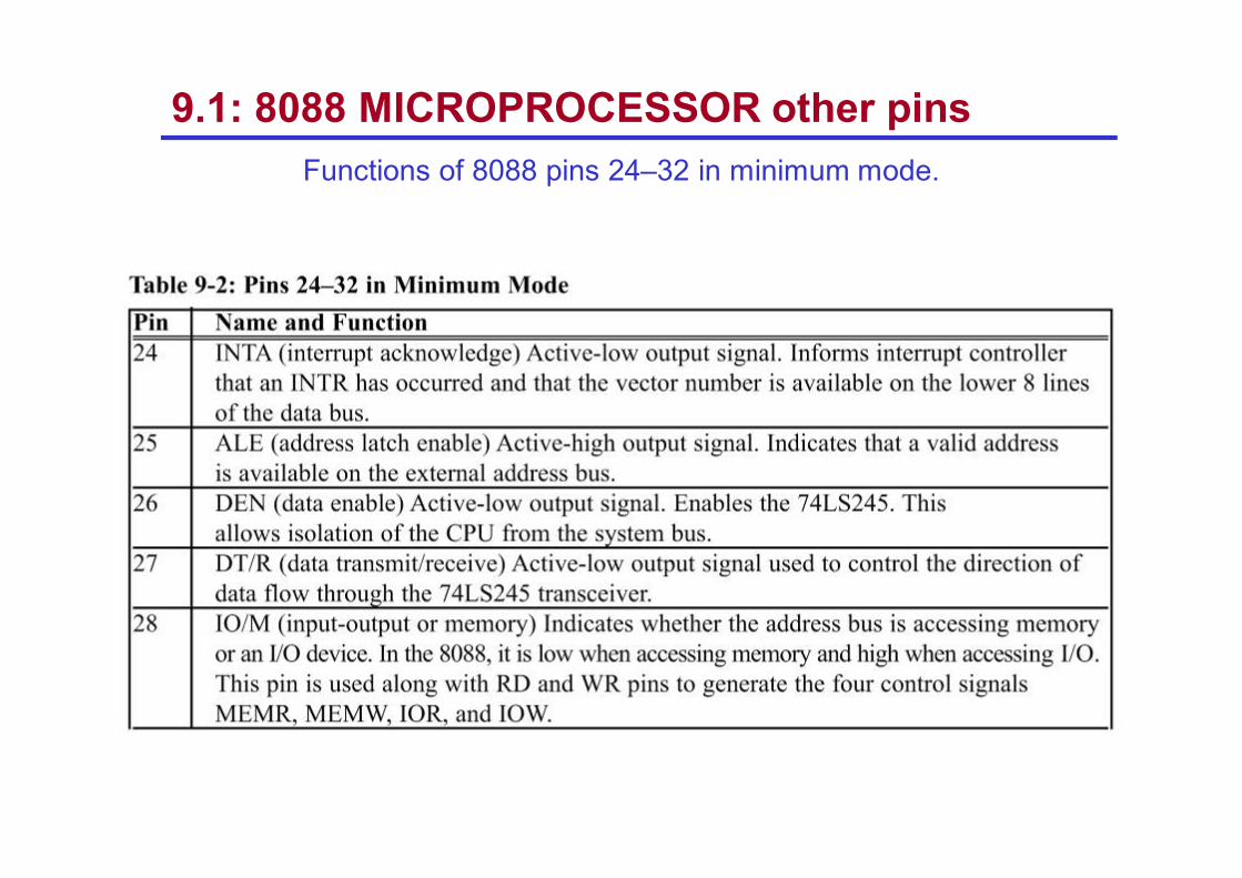
9.1: 8088 MICROPROCESSOR other pinsFunctions of 8088 pins 24–32 in minimum mode.
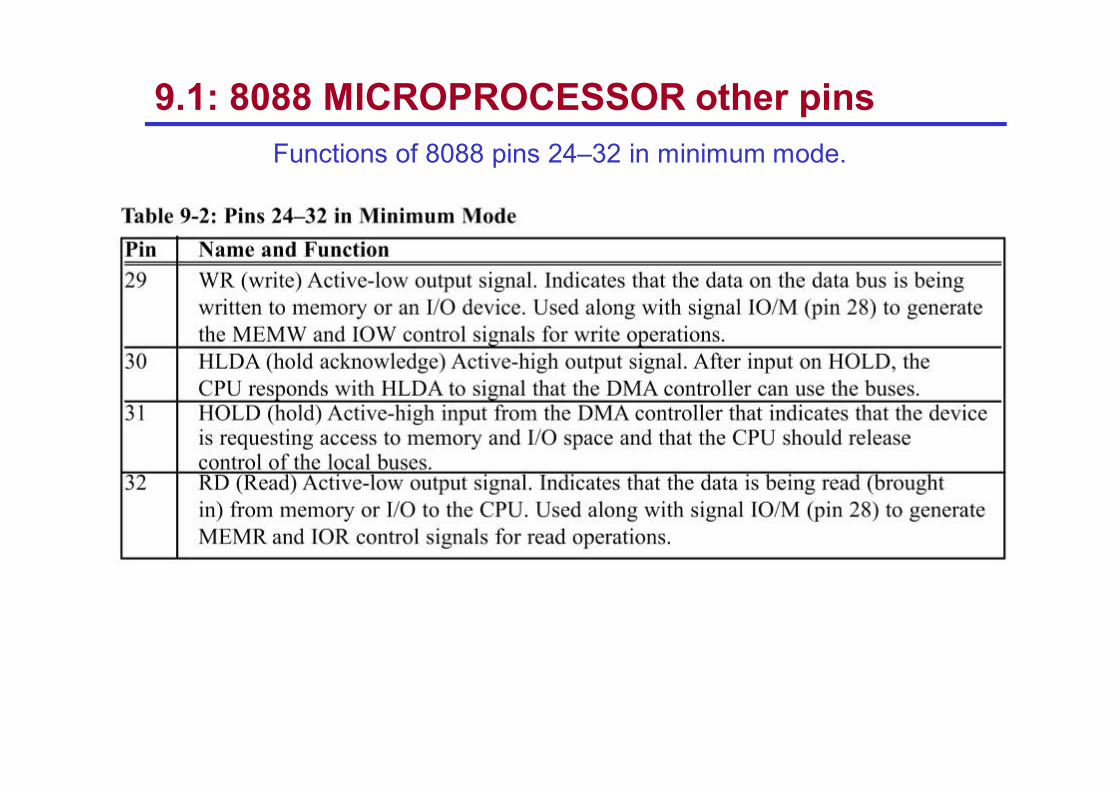
9.1: 8088 MICROPROCESSOR other pinsFunctions of 8088 pins 24–32 in minimum mode.
27
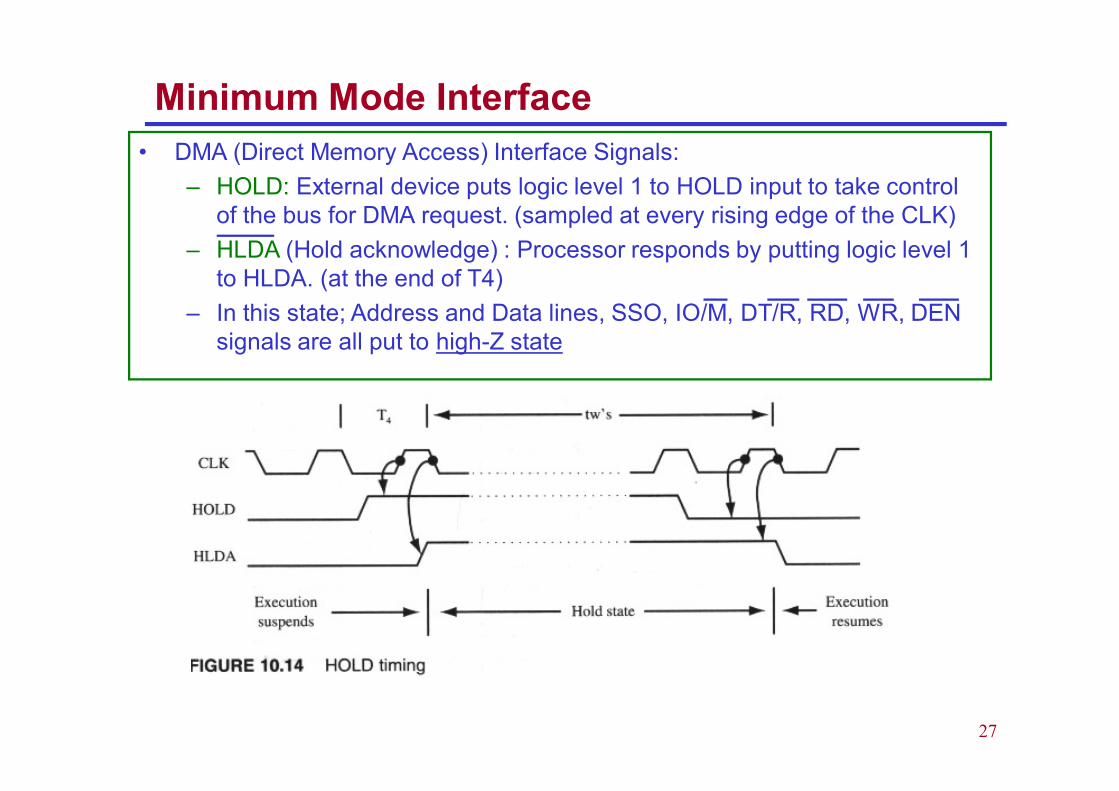
Minimum Mode Interface• DMA (Direct Memory Access) Interface Signals:
– HOLD: External device puts logic level 1 to HOLD input to take control of the bus for DMA request. (sampled at every rising edge of the CLK)
– HLDA (Hold acknowledge) : Processor responds by putting logic level 1 to HLDA. (at the end of T4)
– In this state; Address and Data lines, SSO, IO/M, DT/R, RD, WR, DENsignals are all put to high-Z state
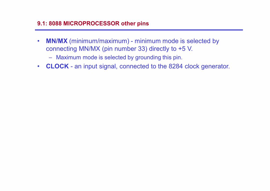
9.1: 8088 MICROPROCESSOR other pins
• MN/MX (minimum/maximum) - minimum mode is selected by connecting MN/MX (pin number 33) directly to +5 V.– Maximum mode is selected by grounding this pin.
• CLOCK - an input signal, connected to the 8284 clock generator.
29
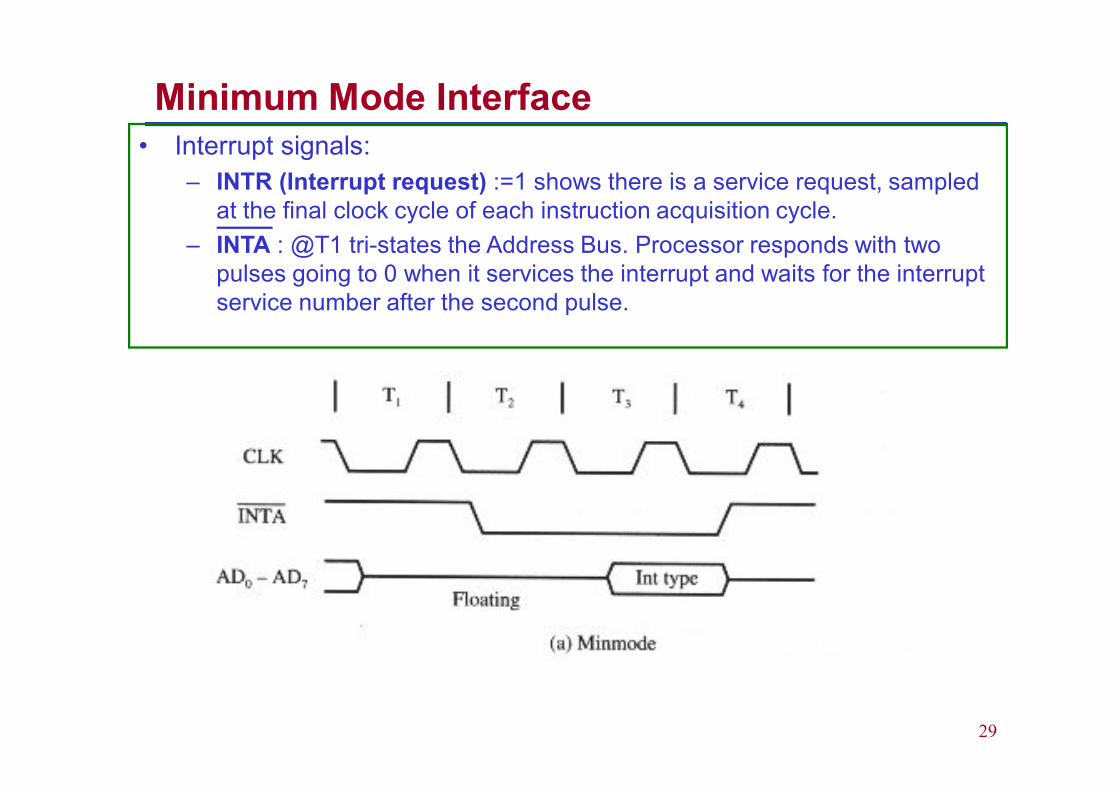
Minimum Mode Interface• Interrupt signals:
– INTR (Interrupt request) :=1 shows there is a service request, sampled at the final clock cycle of each instruction acquisition cycle.
– INTA : @T1 tri-states the Address Bus. Processor responds with two pulses going to 0 when it services the interrupt and waits for the interrupt service number after the second pulse.
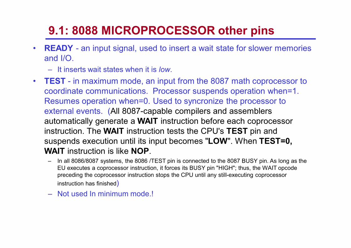
9.1: 8088 MICROPROCESSOR other pins• READY - an input signal, used to insert a wait state for slower memories
and I/O. – It inserts wait states when it is low.
• TEST - in maximum mode, an input from the 8087 math coprocessor to coordinate communications. Processor suspends operation when=1. Resumes operation when=0. Used to syncronize the processor toexternal events. (All 8087-capable compilers and assemblers automatically generate a WAIT instruction before each coprocessor instruction. The WAIT instruction tests the CPU's TEST pin and suspends execution until its input becomes "LOW". When TEST=0, WAIT instruction is like NOP.
– In all 8086/8087 systems, the 8086 /TEST pin is connected to the 8087 BUSY pin. As long as the EU executes a coprocessor instruction, it forces its BUSY pin "HIGH"; thus, the WAIT opcodepreceding the coprocessor instruction stops the CPU until any still-executing coprocessor instruction has finished)
– Not used In minimum mode.!
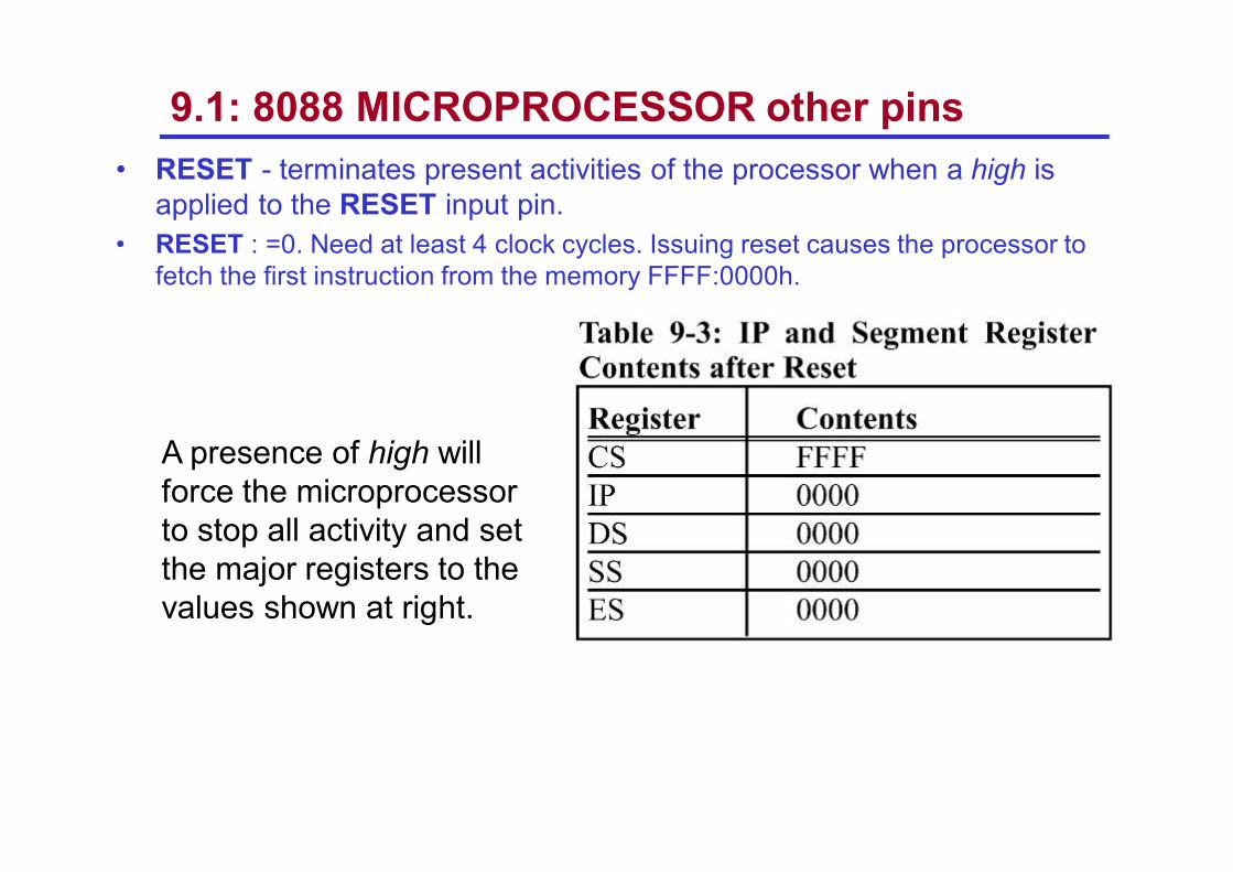
9.1: 8088 MICROPROCESSOR other pins• RESET - terminates present activities of the processor when a high is
applied to the RESET input pin. • RESET : =0. Need at least 4 clock cycles. Issuing reset causes the processor to
fetch the first instruction from the memory FFFF:0000h.
A presence of high will force the microprocessor to stop all activity and set the major registers to the values shown at right.
32
Interrupt Signals cont’d
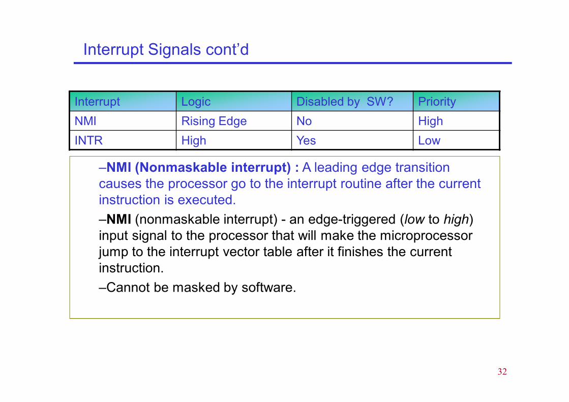
–NMI (Nonmaskable interrupt) : A leading edge transitioncauses the processor go to the interrupt routine after the currentinstruction is executed.–NMI (nonmaskable interrupt) - an edge-triggered (low to high) input signal to the processor that will make the microprocessor jump to the interrupt vector table after it finishes the current instruction. –Cannot be masked by software.
Interrupt Logic Disabled by SW? PriorityNMI Rising Edge No HighINTR High Yes Low
33
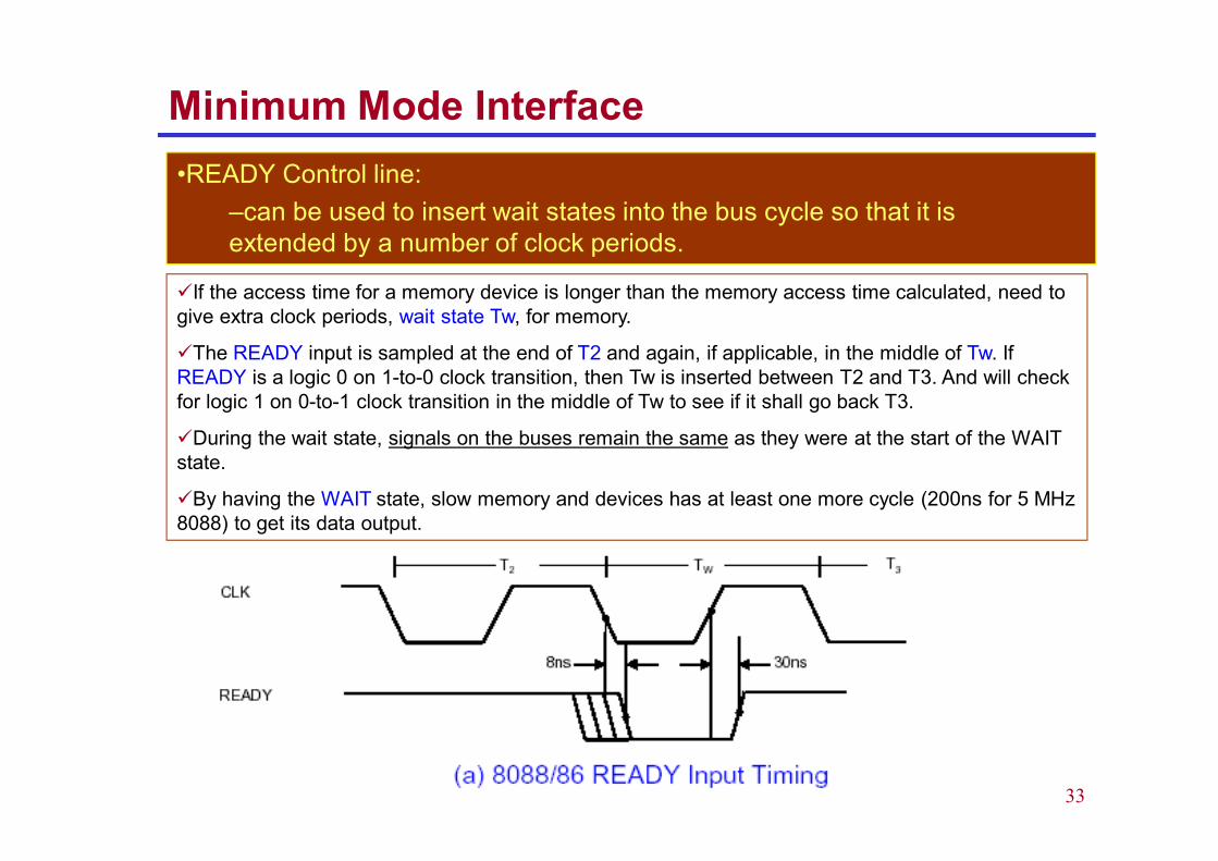
Minimum Mode Interface•READY Control line:
–can be used to insert wait states into the bus cycle so that it is extended by a number of clock periods.
If the access time for a memory device is longer than the memory access time calculated, need to give extra clock periods, wait state Tw, for memory.
The READY input is sampled at the end of T2 and again, if applicable, in the middle of Tw. If READY is a logic 0 on 1-to-0 clock transition, then Tw is inserted between T2 and T3. And will check for logic 1 on 0-to-1 clock transition in the middle of Tw to see if it shall go back T3.
During the wait state, signals on the buses remain the same as they were at the start of the WAIT state.
By having the WAIT state, slow memory and devices has at least one more cycle (200ns for 5 MHz 8088) to get its data output.
34
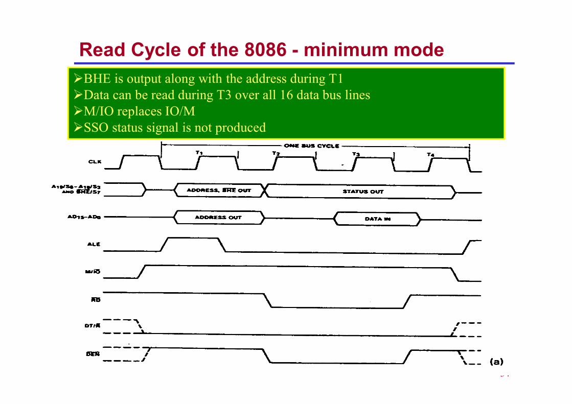
Read Cycle of the 8086 - minimum modeBHE is output along with the address during T1Data can be read during T3 over all 16 data bus linesM/IO replaces IO/M SSO status signal is not produced
35
Address Bus Latches and Buffersc oc
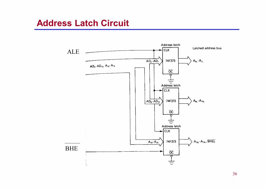
36
Address Latch Circuit
ALE
BHE
37
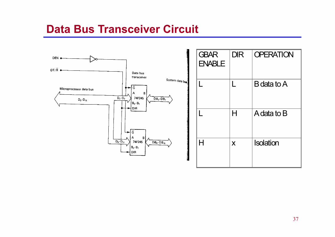
Data Bus Transceiver Circuit
GBARENABLE
DIR OPERATION
L L B data to A
L H A data to B
H x Isolation
38
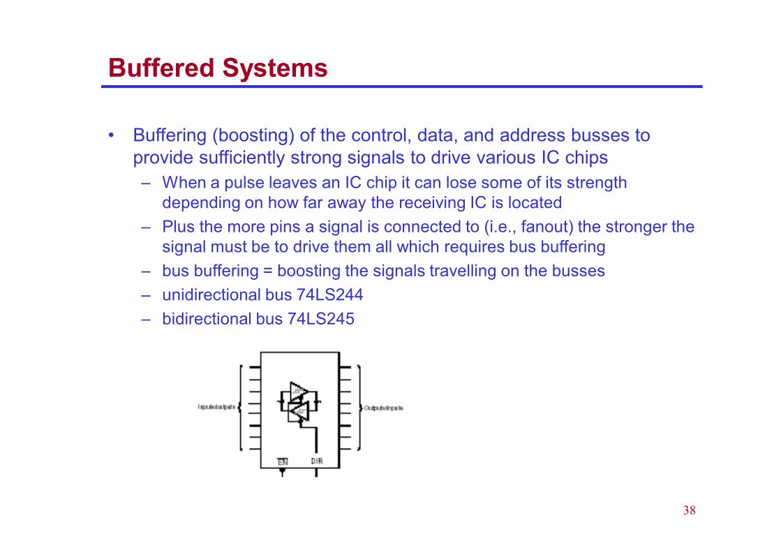
Buffered Systems
• Buffering (boosting) of the control, data, and address busses to provide sufficiently strong signals to drive various IC chips– When a pulse leaves an IC chip it can lose some of its strength
depending on how far away the receiving IC is located– Plus the more pins a signal is connected to (i.e., fanout) the stronger the
signal must be to drive them all which requires bus buffering– bus buffering = boosting the signals travelling on the busses– unidirectional bus 74LS244– bidirectional bus 74LS245
39
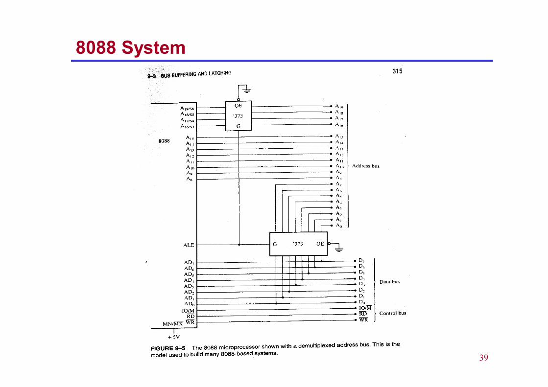
8088 System
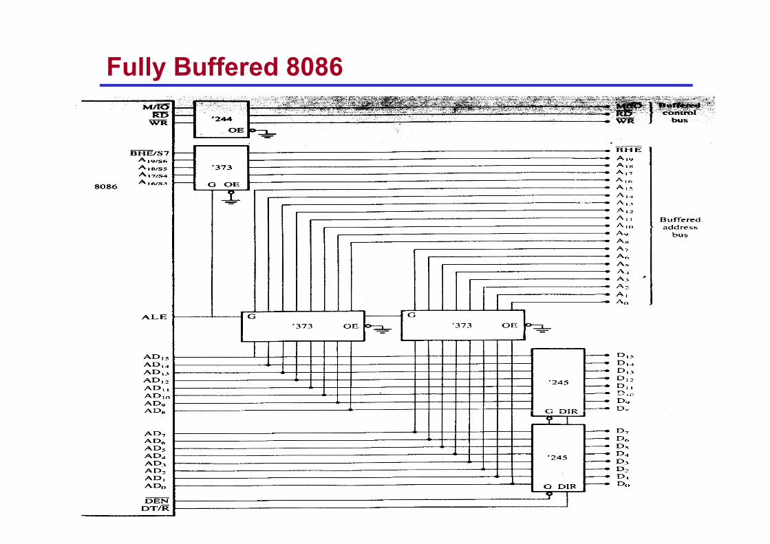
40
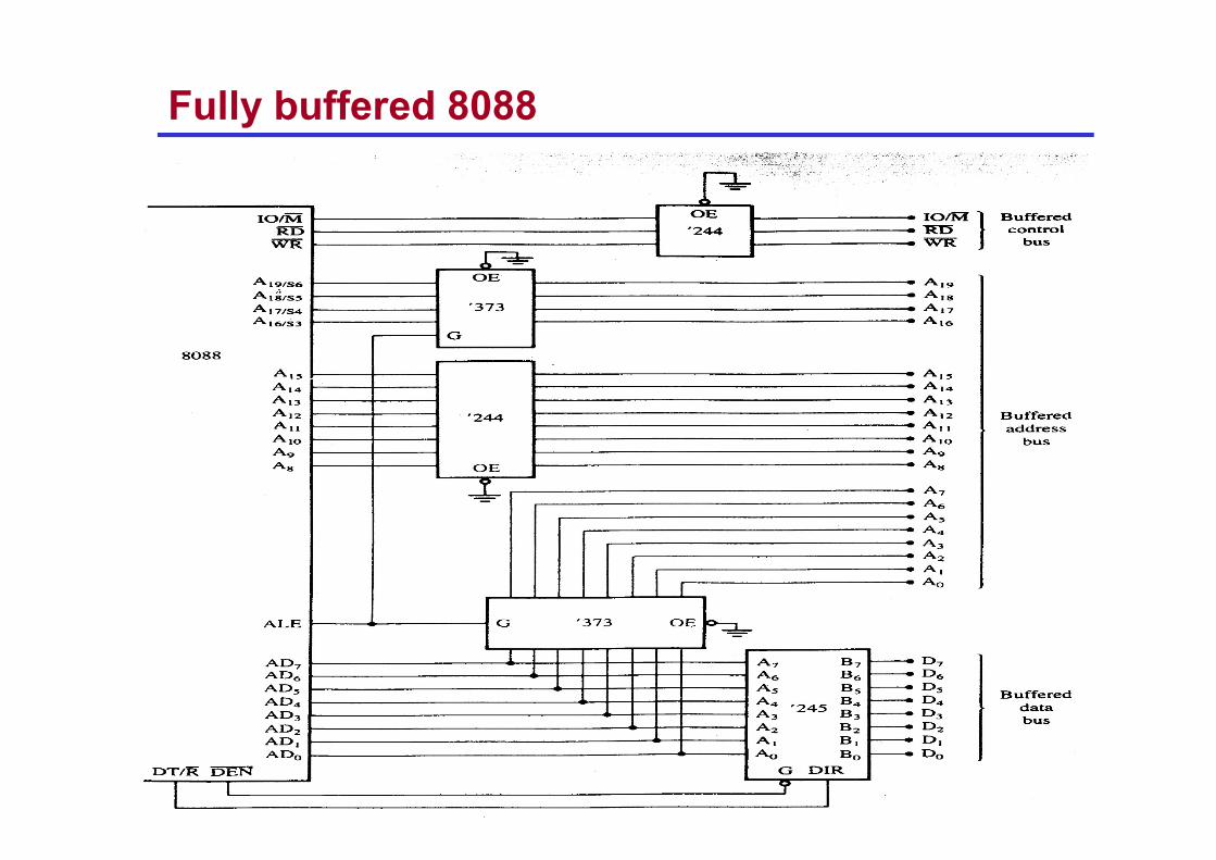
Fully buffered 8088
41
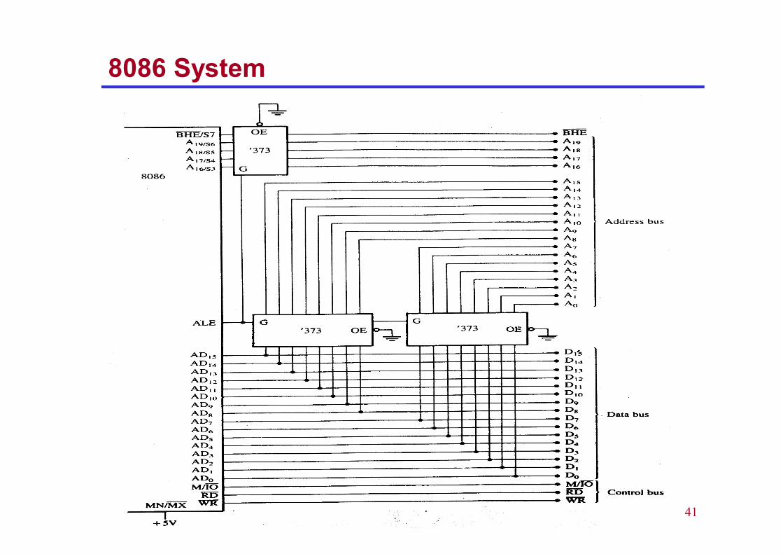
8086 System
42
Fully Buffered 8086
43
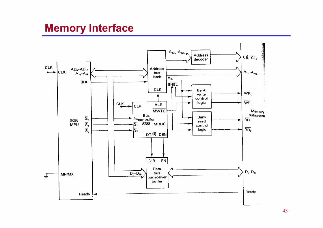
Memory Interface

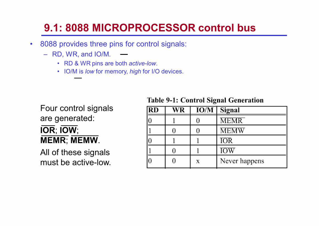
9.1: 8088 MICROPROCESSOR control bus• 8088 provides three pins for control signals:
– RD, WR, and IO/M. • RD & WR pins are both active-low. • IO/M is low for memory, high for I/O devices.
Fig. 9-4 Control signal generation
9.1: 8088 MICROPROCESSOR control bus• 8088 provides three pins for control signals:
– RD, WR, and IO/M. • RD & WR pins are both active-low. • IO/M is low for memory, high for I/O devices.
Four control signalsare generated:IOR; IOW; MEMR; MEMW. All of these signalsmust be active-low.
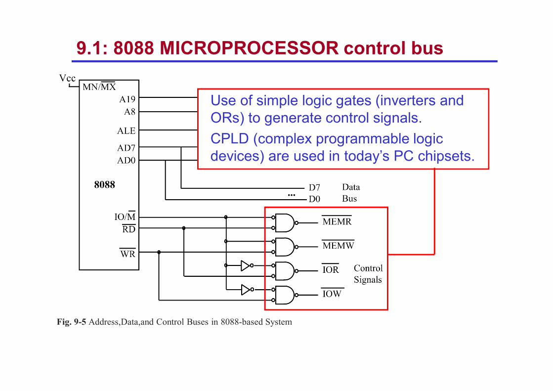
9.1: 8088 MICROPROCESSOR control bus
Use of simple logic gates (inverters and ORs) to generate control signals. CPLD (complex programmable logic devices) are used in today’s PC chipsets.
Fig. 9-5 Address,Data,and Control Buses in 8088-based System
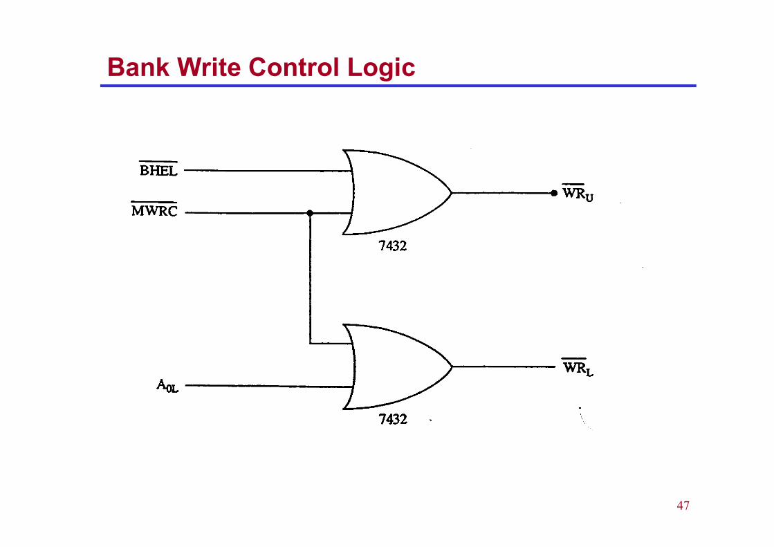
47
Bank Write Control Logic
48
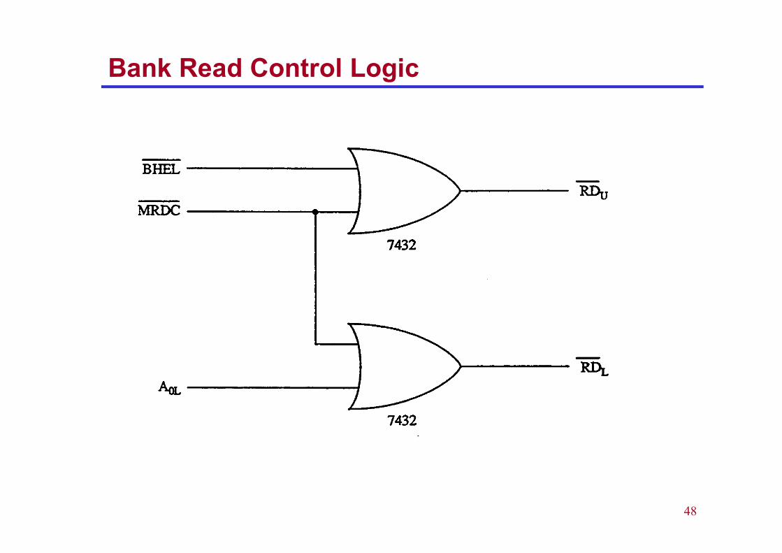
Bank Read Control Logic