Week 14 - organic-electronics.engin.umich.edu
30
Organic Electronics Stephen R. Forrest Week 14 Thin Film Transistors 2 Ambipolar and Other Transistor Architectures Morphology Reliability Applications Chapter 8.3.2-8.4, 8.6-8.9 1
Transcript of Week 14 - organic-electronics.engin.umich.edu

Organic ElectronicsStephen R. Forrest
Week 14
Thin Film Transistors 2
Ambipolar and Other Transistor ArchitecturesMorphology
ReliabilityApplications
Chapter 8.3.2-8.4, 8.6-8.91

Organic ElectronicsStephen R. Forrest
Ambipolar OTFTs• Channel capable of supporting both electron and hole transport
• Advantage: Complementary logic possible with a single structure
VGS VDS
Channel
InsulatorS D
G
x0
np Accumulation region
Strategies for achieving bipolar action:• Use material with both high µFEn and µFEp with contacts in the middle of the
energy gap (i.e. use ambipolar conducting organics)• Use a bilayer, one with higher electron vs. hole mobility and vice versa• Use a blend of electron and hole transporting materials
2

Organic ElectronicsStephen R. Forrest
Ambipolar transfer characteristics
ID =WCi
LµFEn VGS −VTn −
VDS
2⎛⎝⎜
⎞⎠⎟
VDS 0 ≤VDS ≤VDSsat
VGS >VT
⎛
⎝⎜⎜
⎞
⎠⎟⎟
ID =WCi
LµFEn VGS −VTn( )2
VDS ≥VGS −VTn
VDS ≤VGS −VTp
⎛
⎝⎜⎜
⎞
⎠⎟⎟
ID =WCi
LµFEn VGS −VTn( )2 + µFEp VDS −VGS +VTp( )2 { } VDS ≥VGS −VTp ≥VGS −VTn
Example: VTp < VTn
Linear regime
Saturation regime
Ambipolar (quadratic) regime
ID =WCi2L
µFEn VGS −VTn( )2
ID =WCi
2LµFEn VGS −VTn( )2 + µFEp VDS −VGS +VTp( )2 { }
ID =WCi
LµFEn VGS −VTn −
VDS
2⎛⎝⎜
⎞⎠⎟
VDS 0 ≤VDS ≤VDSsat
VGS >VT
⎛
⎝⎜⎜
⎞
⎠⎟⎟n
VT = 0
3

Organic ElectronicsStephen R. Forrest
Bilayer ambipolar OTFT
Disadvantage of the ambipolar OTFT: Ion/Ioff is small since no condition where one carrier type is completely absent.
4Wang et al., Appl. Phys. Lett. 88, 133508 (2006)
Common source amplifier response
•
•
VDD
VIN
•VOUT

Organic ElectronicsStephen R. Forrest
OTFT Bandwidth
5
vDSvGS gmVGS gD!"#$
iD DG
SS
RL
!"%$Small signal equivalent circuit
CGS’=total gate-source capacitance (including parasitics)CGD’=total gate-drain capacitanceRL = external load resistance
iGS =WLCG∂vGS∂t
VDS
= jω WLCG( )vGS = j2π f WLCG( )vGSSmall signal input (gate) current:
iD ! gmvGSSmall signal output (drain) current:
The maximum transistor bandwidth is reached when the current gain 1 iDiG
=
From these expressions, we get the cutoff, or transfer frequency:
CM = Miller capacitance fT =
gm
2πWLCG
=gm
2πWL CGS + CM( )⇒

Organic ElectronicsStephen R. Forrest
Contact Resistance Limits OTFT PerformanceSources of Parasitic Resistance and Capacitance
′gm =
gm
1+ rS gm ′gD =
gD
1+ rS + rD( )gD
This leads to corrected transconductance and output conductance...
... and frequency response
fT =µFE0 VGS −VT( )2πL L + ΔL( )
11+WµFE0CG VGS −VT( )RC L⎡
⎣⎢
⎤
⎦⎥
Hoppe, et al., Organic Electron., 11, 626 (2010)
𝑅! = 𝑟" + 𝑟#
Organic ElectronicsStephen R. Forrest
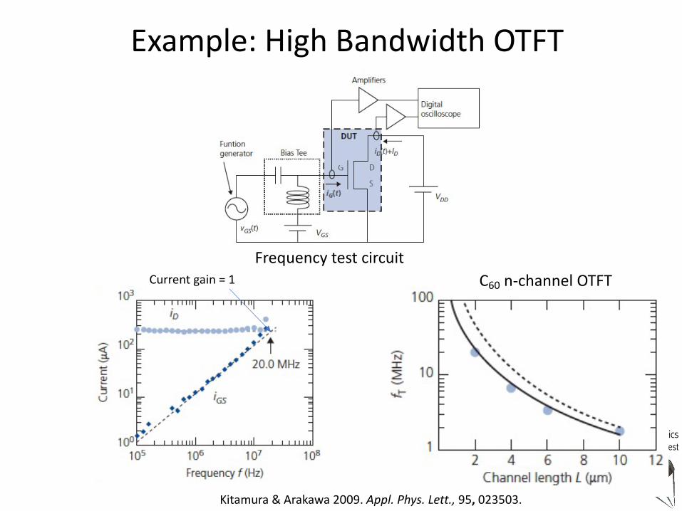
Example: High Bandwidth OTFT
Frequency test circuitCurrent gain = 1
Kitamura & Arakawa 2009. Appl. Phys. Lett., 95, 023503.
C60 n-channel OTFT

Organic ElectronicsStephen R. Forrest
Performance has come a long way
VDD
p-channel
n-channel
Zschieschang, et al., 2017. Organic Electronics, 49, 179.
7 stage ring oscillator
2 fosc = 1 Nτ delayfdelay = 2τ delay( )−1 < fT
8
Smith et al., Appl. Phys. Lett., 93, 253301 (2008) Zschieschang, et al., 2013. Organic Electronics, 14, 1516.
Oscillation frequency a function of the delay per gate

Organic ElectronicsStephen R. Forrest
Dual gate transistors• Useful for adjusting VT due to extra bias control of the second (bottom) gate
• In conventional CMOS technology, this is the “body potential”
• Important for controlling large ICs
ΔVTT =CBCTVGB
9Spijkman et al. Appl. Phys. Lett., 92 143304 (2008)
Shift in top gate threshold related to bottom gate voltage:

Organic ElectronicsStephen R. Forrest
Dual gate control
Improved noise marginControl of circuit gain
Photograph of a 64-bit RFID transponder operating at 4.3 kb/s using dual gate inverter logic.
10
Spijkman et al. Appl. Phys. Lett., 92 143304 (2008)
Myny et al. IEEE J. Sol. State Circuits, 46, 1223 (2011)

Organic ElectronicsStephen R. Forrest
Other Device TypesV-gate transistor
Knife edge cuts through contact layers
Vertical geometries reduce channel transit times ⇒ higher bandwidthCan be more compact than lateral OTFTsCan run in vertical mode (S=E1, D=E2) or horizontal mode (S=E1, D=E3)
Channel and gate insulator deposited
Stutzman, et al., Science, 299, 1881 (2003)

Organic ElectronicsStephen R. Forrest
12
Other Device TypesPermeable gate transistor
Gate (removed from S bygate dielectric) controls S-D current by attraction or repulsion of charge
Permeable source V-FET
Patterned Au S grid
Ben-Sasson et al., (2009). Appl. Phys. Lett., 95, 302.
Permeable Base transistor
Klinger et al. (2017). Scientific Reports, 7, 44713.
Organic ElectronicsStephen R. Forrest
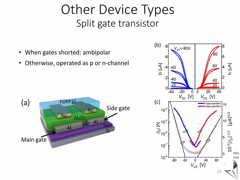
Other Device TypesSplit gate transistor
• When gates shorted: ambipolar
• Otherwise, operated as p or n-channel
Sidegate
Maingate
(a)
(b)
(c)VDS[V]VDS[V]
VGS[V]
10-3|I
D|1/2 [µA
]1/2
-20-40
-60
VGS=-80V
40
60
80
20
Sidegate
Maingate
(a)
(b)
(c)VDS[V]VDS[V]
VGS[V]
10-3|I
D|1
/2[µ
A]1/2
-20-40
-60
VGS=-80V
40
60
80
20
13

Organic ElectronicsStephen R. Forrest
Highest mobilities when π-stacking is in the transistor plane
14
Different, common organic stacking motifs(see Chapter 2)
best in-planeconduction
best verticalconduction

Organic ElectronicsStephen R. Forrest
15
Methods for Orienting the Channel Semiconductorsolution shearing
1 mm1 mm
shear dir.
Liu, et al., Z. (2009) Adv. Materials, 21, 1217
dip coating TIPS-pentacenechannel strips
Jang et al., (2012) Adv. Functional Materials, 22, 1005
zone casting
Miskiewicz, et al. (2006). Chem. Materials, 18, 4724.
S D

Organic ElectronicsStephen R. Forrest
16
Achieving Optimal Morphologies• Method 1: Control during growth by VTE, OVPD, solution • Method 2: Use Self Assembled Monolayer (SAM)
functionalization to initiate growth of desired structures by vapor or solution deposition
Example: Octyltrichlorosilane (OTS)
0PO O
O
_ _
PO O
O
_ _
PO O
O
_ _
PO O
O
_ _
PO O
O
_ _
PO O
O
_ _
GateInsulator

Organic ElectronicsStephen R. Forrest
Contact Printing Initiated by SAM
Pentacene (p)F16CuPc (n)
17Zschieschang, et al., 2008. Langmuir, 24 1665.

Organic ElectronicsStephen R. Forrest
Reliability• Threshold voltage drift the primary source of circuit failure
• Decreasing noise margin• Increasing leakage
VGS (V) VGS (V)
I D(nA)
(b)(a)
Drift RecoveryVDS = -3VVGS = -20V
18Sharma, et al. Phys. Rev. B, 82 075322 (2010).
Original transfer characteristics (and VT) partially recovered following stress

Organic ElectronicsStephen R. Forrest
Threshold voltage drift over time• Drift due to charges migrating in insulator or channel toward the
interface• Surface traps at the channel• Traps within the semiconductor bulk• Charge (ions) drifting within the insulator
ΔVT t( ) = ΔVT ∞( ) 1− exp − t
τ⎛⎝⎜
⎞⎠⎟
m⎛
⎝⎜
⎞
⎠⎟
τ = 2πν( )−1exp ET kBT( )
m = T/T0 for exponential trap distribution given by:
⇒ Time constant for drift
htr E( ) = htr0 exp − E ET( )
Drift occurs over an extended time, and is thermally activated19
Empirical voltage drift expression:Stretched exponential
(see Ch. 6.7 & 7.8)

Organic ElectronicsStephen R. Forrest
Example: Poly(triarylamine)
m
Stretchedexponential
(a)
(b)
(a) (b)
P
IDID
S
VGT(V)
-20V
+20V0V
ΔVTB
(V)
VGT
VGB(V)
|I D| (A)
2H2O ↔ 4H + + O2 + 4e−
Water is the main problem: Proton generation
20Bobbert et al, Adv. Mater. 24, 1146 (2012) Mathijessen et al., Adv. Mater. 22, 5105 (2010)

Organic ElectronicsStephen R. Forrest
Hysteresis: Another failure mode
VDS (V)
VDS (V)
I D/C i
(µA-cm
2 /nF)
I D/C i
(µA-cm
2 /nF)
BG/TC
BG/BC
p-channel F8T2 transistors
Drain contact trapping
21Richards & Sirringhaus Appl. Phys. Lett., 92, 023512 (2008)
Contact only via edge of the electrodes increases the current density, resulting in defect formation and charge trapping. This induces changes in VT and IDS, depending on sweep direction (arrows)
BG/TC: Large contact area to channelCurrent drawn from contact surface (arrow)
S D
G
channel
S D
G
BG/BC: Small (edge) contact to channelCurrent drawn from contact edge (arrow)

Organic ElectronicsStephen R. Forrest
Comparison of TFT Reliabilities
Caveats (and there are many):• Devices from different labs may be based on different standards and conditions• Device selection not necessarily based on same characteristics • Performance can vary over a wide range in any technology
Jia, et al. Science Adv. 4, eaao1705, (2018)

Organic ElectronicsStephen R. Forrest
Applications must exploit advantages, and cannot be vulnerable to disadvantages
• PROsØ Flexible, conformable, ultralightØCan be made over very large areasØSuitable for large scale R2R manufacture
• CONsØCannot source large currentsØCharacteristics drift over long periods in operationØLimited bandwidth (≤ 1 MHz in many cases)
To review….
23
Organic ElectronicsStephen R. Forrest
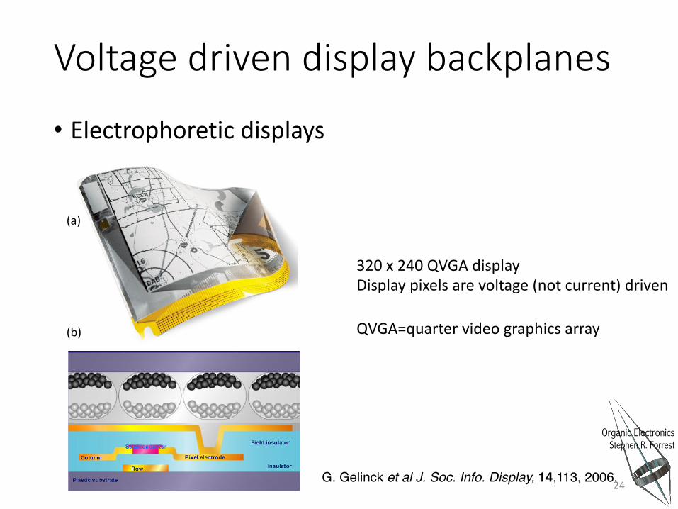
Voltage driven display backplanes
• Electrophoretic displays
(a)
(b)
320 x 240 QVGA displayDisplay pixels are voltage (not current) driven
QVGA=quarter video graphics array
G. Gelinck et al J. Soc. Info. Display, 14,113, 2006.24

Organic ElectronicsStephen R. Forrest
Thermal Position Sensing
Ren, et al., Adv. Mater. 28, 4832 (2016)
Sensing element: channel resistance with a Ag NP layer
Array used for detecting position of thermal source

Organic ElectronicsStephen R. Forrest
Chemical sensing• OTFTs have demonstrated voltage drifts due to water. • Are there other analytes that can be sensed?• Sensor attributes
• Fast• Sensitive to small doses• Reversible• Specific
a-6T transistor
B. Crone et al., 78, 2229, (2001)
DID
Analyte: 1-hexanolExposure: 5 sRecovery: 1 min
16 analytes11 transistor channel mater.
DID
26

Organic ElectronicsStephen R. Forrest
Bendable Electronics
Encapsulation
Substrate
Activeelectronics
dsub
de
=Ye
Ysub
Neutral strain:
(a)
2mm
(b)
1cm
12x12 array of tactile pixels
Y = Young’s modulus (measure of material stiffness)
𝑌 =𝐹𝐿!𝐴∆𝐿
F = force to extend solidL0 = original lengthDL = length changeA = cross sectional area perpendicular to F
27
Placing active electronics at the neutral strain point⇒ minimal stress to circuits on bending even over sharp angles
Kaltenbrunner et al. Nat. Commun.3, 770 (2012); Nature 499, 458 (2013)

Organic ElectronicsStephen R. Forrest
“Imperceptible” Electronics
Kaltenbrunner, et al., Nature, 499, 458 (2013).
Substrates are 1 µm thick!
28

Organic ElectronicsStephen R. Forrest
In Vivo Cardiac Monitoring
Sekitani, et al. Nat. Comm. DOI: 10.1038/ncomms11425 (2016)29

Organic ElectronicsStephen R. Forrest
What we learned• OTFTs have made extraordinary progress since their
first demonstration in 1986• Their properties can be modified through chemical
design• Morphology is key to high performance• Very small gate transistors are common in BG/TC
configurations• Very large circuits demonstrated (100’s of transistors)• Reliability depends on exposure to contaminants• Most promising applications in sensing and medicine• But….there is no “killer app” yet identified that can
drive this technology to a commercial success30