Week 2-12 - Organic Electronics: Foundations to Applications

Organic ElectronicsStephen R. Forrest
Week 10Light emitters 3
Outcoupling StrategiesReliability
Chapter 6.6.2-6.7
1

Organic ElectronicsStephen R. Forrest
Substrate Mode Outcoupling: ~2X Improvement
ηext~40%
Microlens arrays: Polymer hemispheres much smaller than pixel
Möller, S. & Forrest, S. R. 2001. J. Appl. Phys., 91, 3324.
Fabrication sequence Spectrum angle independent
⇐ Scattering and surface roughness also can reduce substrate modes
Reidel, et al., Opt. Express 18 A631 (2010) Chang, et al., J. Appl. Phys., 113 204502 (2013) 2

Organic ElectronicsStephen R. Forrest
3
Metal electrode pixel
Organics
Low-index grid
ITO
Glass substrate
Ray BRay A
Ray
C
Side view
wLIG
worg
Waveguide Mode Outcoupling:Embedded Low Index Grid
ηext~60% (incl. substrate modes)
Sun, Y. & Forrest, S. R. 2008. Nature Photon., 2, 483.

Organic ElectronicsStephen R. Forrest
4
2µm
Low Index Grid Images
• OLED >> Grid size >> Wavelength• Embedded into OLED structure• May partially decouple waveguide mode from SPPs

Organic ElectronicsStephen R. Forrest
5
400 600 8000.0
0.5
1.0
Nor
m. E
L (a
.u.)
Wavelength (nm)
Dev. 1 Dev. 4
10-6 1x10⁻⁵ 1x10⁻⁴ 10-3 10-2 10-1
0
10
20
30
Pow
er E
ffici
ency
(lm
/W)
Exte
rnal
Qua
ntum
Effi
cien
cy (%
)
Current Density (mA/cm2)
Dev. 4 Dev. 3 Dev. 2 Dev. 1
0
10
20
30
40
50
60
70
80
Dev. 1 x 1.32
Dev.1x1.68
Dev. 1 x 2.3
10-3 10-2 10-1 100 101 10210-3 10-2 10-1 100 101 102
Hybrid WOLED Performance Using Embedded Grids + Microlens Arrays
Device 1: ConventionalDevice 2: LIG onlyDevice 3: Microlenses onlyDevice 4: LIG + Microlenses
Method is WavelengthIndependent
Sun, Y. & Forrest, S. R. 2008. Nature Photon., 2, 483.
Organic ElectronicsStephen R. Forrest
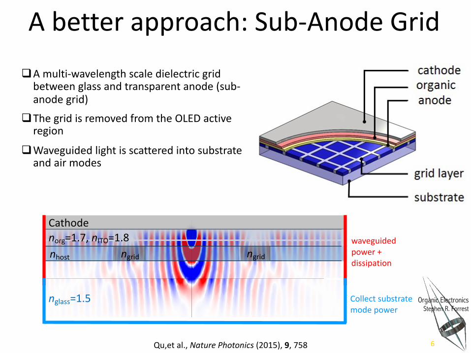
A better approach: Sub-Anode Grid
qA multi-wavelength scale dielectric grid between glass and transparent anode (sub-anode grid)
qThe grid is removed from the OLED active region
qWaveguided light is scattered into substrate and air modes
6
Cathode
nglass=1.5
nhost
norg=1.7, nITO=1.8ngridngrid
waveguided power + dissipation
Collect substrate mode power
Qu,et al., Nature Photonics (2015), 9, 758

Organic ElectronicsStephen R. Forrest
Emission field calculations
7
WITH GRID
WITHOUT GRID
VERTICAL DIPOLE
HORIZONTAL DIPOLE
Mostly in-plane(Waveguided)
Mostly out-of-plane(Glass + air)
Qu,et al., Nature Photonics (2015), 9, 758

Organic ElectronicsStephen R. Forrest
Optical Power Distribution
Thick-ETL organic structure:
340nm grid/70nm ITO/2nm MoO3/40nm TcTa/15nm CBP: Ir(ppy)3/10nm TPBi/230nm Bphen:Li/Al
2nm MoO3/40nm CBP/15nm CBP:Ir(ppy)3/xnm TPBi/1nm LiF/Al
Qu,et al., Nature Photonics (2015), 9, 758 8

Organic ElectronicsStephen R. Forrest
Al OrganicITO
SEMLA
High IndexSpacer layer
Getting All the Light Out: Sub-Electrode Microlens Array (SEMLA)
Qu, Y., et al. 2018. ACS Photonics, 5, 2453. 9

Organic ElectronicsStephen R. Forrest
0 20 40 60 80 100 120 1400
20
40
60
80
100
Frac
tion
of P
ower
(%)
ETL thickness (nm)
SPPLoss
WV
SEMLA
0 20 40 60 80 100 120 1400
20
40
60
80
100
Frac
tion
of P
ower
(%)
ETL thickness (nm)
SPP
WV
SubAir
Loss
SEMLAs Change the Outcoupling Landscape
Qu, Y., et al. 2018. ACS Photonics, 5, 2453.10

Organic ElectronicsStephen R. Forrest
0 5 1010-7
10-3
101
Con SEM LA
J (
mA
/cm2 )
Vo ltage (V )
102 103 1040
20
40
60
80 Con_air Con_IMF SEMLA_air SEMLA_MLA SEMLA_IMF Sap_IMF
h EQE (%
)
Brightness (cd/m2)
-90
-60
-300
30
60
90 L am b. C on S E M L A M LA S E M LA H S
SEMLA
SEMLA
+MLA
SEMLA
+IMF
Sap1.0
1.5
2.0
2.5
3.0
3.541±3 %45 ±4%
2 7±3 %2 0±2 % 60 ±4%
65 ±5%
47 ±4%
E F
30±3 %
SEMLA Performance
Qu, Y., et al. 2018. ACS Photonics, 5, 2453. 11

Organic ElectronicsStephen R. Forrest
Diffuse Reflectors: Low Cost & Simple
Teflon is the best diffuse dielectric reflector
Diffuse (Green) Mirror (Green) Diffuse (White) Mirror (White)
0.01 0.1 1 100
10
20
30
40
50
h EQE
(%)
Current Density (mA/cm2)
PHOLED Active Area
Kim, J., et al. (2018), ACS Photonics, 5, 3315. 12

Organic ElectronicsStephen R. Forrest
Pt(dbq)(acac)
Isotropic Orientation
HorizontalOrientation
Outcoupling Enhancements by Molecular Orientation
Ir(ppy)3
Prevents coupling to SPPs and waveguide modes
Planar molecules (e.g. Pt-complexes) more likely to align than octahedral (tris-Ir complexes)13

Organic ElectronicsStephen R. Forrest
Example results
0 10 20 30 40 50 60 70 80 900.0
0.5
1.0
1.5
2.0
2.5
Detector Angle [Degree]N
orm
aliz
ed In
tens
ity
Isotropic (qhor= 66.7%) Horizontal (qhor= 100%) Fit (qhor= 45.9%) CBP:Pt(dbq)(dpm) 8wt%
Pt(dbq)(dpm)
0 10 20 30 40 50 60 70 80 900.0
0.5
1.0
1.5
2.0
Detector Angle [Degree]
Nor
mal
ized
Inte
nsity
Isotropic (qhor= 66.7%) Horizontal (qhor= 100%) Fit (qhor= 65.9%) CBP:Irppy3 8wt%
Ir(ppy)3
Approach challenges• Added constraints on molecular design• Added constraints on process (growth) conditions: may not align as expected• Added constraints on device architecture• Alignment is never “perfect”: only modest improvements
Θ =
TM!
TE⊥ +TM⊥ +TM!
Ratio of light emitting by vertical to horizontal dipoles:
14

Organic ElectronicsStephen R. Forrest
• Waveguide thickness varies due to the corrugation.
• As the thickness changes, the mode distribution changes.
• When the waveguided power travels from thin to thick areas, the k vector needs to change direction to keep “being trapped”. Otherwise, the light is extracted.
0.8 0.85 0.9 0.95 10
0.5
1
1.5
2
2.5
3
3.5 x 10⁻³
k||/k
powe
r int
ensit
y
10nm30nm50nm70nm90nm
TM0
TE0
ETL thickness
Waveguide
nsub/norg=0.88
W. H. Koo, et al, Nat. Photonics 2010, 4, 222.
A possible approach: Surface buckling?FFT
Al on resin
Substrate Corrugations Can Outcouple Waveguide Modes
15

Organic ElectronicsStephen R. Forrest
Reliability Testing Methodologies• Need to set clear metrics for failure
ØExample: Operating time for initial luminance (L0) to decrease 10% from its initial value (called T90, or LT90)
ØEmploy a population of equivalent devices and monitor their performance parameter (e.g. luminance) under normal operating conditions
ØIf degradation slow, then an empirical degradation relationship is determined to extrapolate time to failure• Example: Stretched exponential function:
• If degradation too slow, need to accelerate via increased T or L0.• Accelerated conditions must not introduce new failure modes• Need empirical relations to normalize lifetime to standard operating
conditions (called acceleration factors)
𝐿 𝑡 = 𝐿!𝑒𝑥𝑝 −𝑡/𝜏 b t, b = empirical constants
LTx L0( ) = LTx L0tst( ) i L0tst
L0
⎡
⎣⎢
⎤
⎦⎥
n
n = empirical acceleration factor16

Organic ElectronicsStephen R. Forrest1/kBTEL
1/(τ
2 jα )
T
Yoshioka, et al.. 2014,SID Digest Tech. Papers, 45, 642.
Meas
1τ 2
= ′′K jα exp −ΔEA0 kBT( )
Accelerated Degradation Methodologies
Sum of lifetimes alternative empirical relation):
DEA0=thermal activation of degradationa = current acceleration factor
Measuring populations of identical devices
L t( ) L0 = λ exp −t / τ1( ) + 1− λ( )exp −t / τ 2( )Burn-in Long term decay
Example data: Green PHOLED
17

Organic ElectronicsStephen R. Forrest
18
Intrinsic Lifetime Limits of OLEDs
Giebink, et al., J. Appl. Phys., 103, 044509 (2008).
HTL ETLEML[mCP/ 9wt% FIr6]
drec
x2x3 xx1
FnE
FvE
HOMOhost
LUMOhost
tE
Guest
DefectJq
Jq
holes electrons
Energy ScaleRed light: ~ 2 eV
Green light: ~2.3 eVBlue light: ~ 2.9 eV

Organic ElectronicsStephen R. ForrestExciton-Polaron Annihilation
1 1/S T
0S
* */n nS T
energytransfer
Exciton-Exciton Annihilation
12
R
1 1/S T
0S
E
q
0D
*nD
energytransfer
2
0S
1 1/S TR
Degradation Routes
• Energetically Driven- Lifetime: R>G>B
• Two particle interactions lead toluminance loss
-Exciton on phosphor, polaronon host
- Exciton-exciton also possible
Triplet energy (~2.8 eV) + polaron (~3.3 eV) = hot polaron (≥ 6 eV)Bond cleavage
Broken bonds? à Defects!
Bond BE(eV) Bond BE(eV)
C-C 3.64 N-N 1.69
C-H 4.28 N-O 2.08
C-O 3.71 N-H 4.05
C-N 3.04 O-O 1.51
C-F 5.03 H-H 4.52
19

Organic ElectronicsStephen R. Forrest
0.0
0.2
0.4
0.6
0.8
1.0
Lum
inan
ce (n
orm
)
2010-1 100 101 102 103
0.0
0.2
0.4
0.6
0.8
1.0
t' (hrs)
Lum
inan
ce (n
orm
)
0.0
0.2
0.4
0.6
0.8
1.0
Lum
inan
ce (n
orm
)L0 = 1000cd/m2
drec = 12nm
L0 = 4000cd/m2
drec = 5nm
L0 = 1000cd/m2
L0 = 4000cd/m2
L0 = 1000cd/m2
L0 = 4000cd/m2
ExcitonLocalization
Exciton-ExcitonAnnihilation
Exciton-PolaronAnnihilation
Luminance Decay vs Time
Defect Generation Rates
•Blue PHOLED•Prepared and packaged using industry std.

Organic ElectronicsStephen R. Forrest
21
8
9
10
11
12
13
14
Volta
ge
10-1 100 101 102 1038
9
10
11
12
13
14
Volta
ge
t' (hrs)
8
9
10
11
12
13
14
Volta
ge
L0 = 4000cd/m2
drec = 5nm
L0 = 1000cd/m2
L0 = 4000cd/m2
L0 = 1000cd/m2, drec = 12nm
L0 = 1000cd/m2
ExcitonLocalization
Exciton-ExcitonAnnihilation
Exciton-PolaronAnnihilation
L0 = 4000cd/m2
Drive Voltage Drift with Aging
•Q~1018 cm-3 50% increase in quenching•At 1000 cd/m2, formation rate = 1012cm-2s-1
-1 in 5 x10⁸ E-P encounters leads to defect-Increasing recombination zone width extends lifetime
- Guest triplets/host polarons most active
Conclusions
Giebink, et al., J. Appl. Phys., 103, 044509 (2008).

Organic ElectronicsStephen R. Forrest200 400 600 800 10001200
0.00.20.4
1.40.00.20.4
1.4
In
tens
ity (a
.u.)
m/z
Unaged
T40
H1-3Alq3
mCBP Ir(dmp)3
E4 D4-7
E3
Ir(dmp)3m/z = 1198
H1m/z = 155
mCBPm/z = 484
H2m/z = 168
H4m/z = 319
D2m/z = 526
H3m/z = 243
D1m/z = 334
D4m/z = 862
D3m/z = 668
Evidence for Defect Formation: Molecular Fragmentation
Jeong, et al. Org. Electron., 64, 15 2019
Laser Desorption Ionization-Time of Flight Mass Spectroscopy(LDI-TOF-MS)
-Molecular species identification
22

Organic ElectronicsStephen R. Forrest
D12.1
0.6
D2-11.6
-12.5
D4-5.6
-8.2
CationAnion Radical Neutral
D6
-3.2
-4.8-4.5 (HOMOIr(dmp) )
-1.15 (LUMOmCBP)
D7
-0.9
-4.6
H1
-0.7
-6.1
H1-3.9
-4.8
H1-12.7
H14.3
H2
-0.7
-5.5
H2
-0.9
-5.4H2-7.9
-9.6
H2
3.6
-0.4
H3
-0.7
-5.3
H3
-2.3
-5.4
H4
-1.0
-5.3H3-7.9
-9.6
H32.1
0.7
H4
-2.2
-5.4H4-7.9
-8.4
H41.3
0.7
Non-trappingElectron traps(electrically active)
Triplet Energy (ET)
0 eV
2.8 eV (ET, Ir(dmp) )
D6<0.6
H1<1.4
H3<2.4
H4<2.8
H13.0
H23.2
H33.2
H43.1
D72.1
3
3
2.9 eV (ET, mCBP )
Identification of Defect Energies
Jeong, et al. Org. Electron., 64, 15 2019
Non-trapping
23

Organic ElectronicsStephen R. Forrest
dopant
host
Con
cent
ratio
n
Position
Conventional Graded
Exciton density
LUMO
HOMO
Emission+
-
+
-
Y. Zhang, et al., Nature Comm. 5 5008 (2014)
Reducing Exciton Density to Increase Lifetime
ETL
HTL

Organic ElectronicsStephen R. Forrest
mCBP mCBP mCBP mCBP
Alq3 Alq3 Alq3 Alq3
Li:Alq3
mCBP
Alq3
HATCN HATCN HATCN
HATCN
HATCN
NPD
mCBPAlq3
Li:Alq3
mCBP
Alq3
HATCN
HATCN
NPD
NPD
Host: mCBP Dopant: Ir(dmp)3
13 vol% uniform 8 to 18% vol% graded
D1 D2 D3 D1S D3S
Spreading the recombination zone: Dopant/Host Grading3 Different test device structures
25

Organic ElectronicsStephen R. Forrest
5.0eV
6.0eVh
eIr (dmp)3
mCBP
e
h
0 10 20 30 40 50 600.00
0.01
0.02
0.03
0.04
0.05 EML of D1
Exci
ton
dens
ity (a
rb. u
nits
)
Distance to anode (nm)
D1 D2 D3 D1S D3S
EMLs of D2, D3 and D4
Excitons in the EML
Exciton Sensing• Red Phosphor (PQIr)• 1.5 nm thick• Placed at 5 nm
intervals in EML• Measure red
emission intensity
Dopant conducts holes
Host conducts electrons
Y. Zhang, et al., Nature Comm. 5 5008 (2014)ETL
HTL
sensing layer positions
26

Organic ElectronicsStephen R. Forrest
10 X Lifetime Improvement Over Conventional
Y. Zhang, et al., Nature Comm. 5 5008 (2014)
0.5
0.6
0.7
0.8
0.9
1.0
0.5
0.6
0.7
0.8
0.9
1.0
0 150 300 450 6000.0
0.5
1.0
1.5
2.0
0 150 300 450 6000.0
0.3
0.6
0.9
1.2
,D 1,D 2,D 3,D 1S,D 3S,T P A ,model,E X P ,model
,
,
Luminan
ce,(no
rm.)
,
,
Luminan
ce,(no
rm.)
,
,
ΔV,(V)
T ime ,(hrs )
,
,
ΔV,(V)
T ime ,(hrs )
10X$
1000 cd/m2
Stacked/Graded
Graded
Conventional
0.5
0.6
0.7
0.8
0.9
1.0
0.5
0.6
0.7
0.8
0.9
1.0
0 150 300 450 6000.0
0.5
1.0
1.5
2.0
0 150 300 450 6000.0
0.3
0.6
0.9
1.2
,D 1,D 2,D 3,D 1S,D 3S,T P A ,model,E X P ,model
,
,
Luminan
ce,(no
rm.)
,
,
Luminan
ce,(no
rm.)
,
,
ΔV,(V)
T ime ,(hrs ),
,
ΔV,(V)
T ime ,(hrs )
10X$
P.Levermore et al, SID Digest, 2011.
Stacking is essential!
Panel15 cm x 15 cm 82% fill factor
2 Unit WSOLED
Luminance [cd/m2] 3,000
Efficacy [lm/W] 48
CRI 86
Luminous Emittance
[lm/m2]7,740
1931 CIE (0.454, 0.426)
LT70 [hrs] 13,000
27

Organic ElectronicsStephen R. Forrest
• Luminance to achieve sRGB color gamut for G is 10X that for B
• ⇒B sub-pixel L0=100 cd/m2 (c.f. G with L0>1,000 cd/m2)
• ⇒B lifetime to T50=70,000 hr.
• Adopting Degradation acceleration factor: n =1.55 with
• ⇒B PHOLED lifetime to T50 = 1.3×10⁵ hr.
• Commercial G PHOLED lifetime = 106 hours at L0 = 1000 cd/m2.
T50(100cd/m2 ) = T50(1000cd/m2 )× 1000cd/m2
100cd/m2
⎡
⎣⎢
⎤
⎦⎥
n
Not blue enough, T95 is required
Dopant Grading: Is it Good Enough?using acceleration factors to predict lifetime
28

Organic ElectronicsStephen R. Forrest
Dopant Grading for Lighting: Is it OK?• Current state of stacked WOLED: T70=13,000 hrs
• Mostly limited by blue lifetime
• Only light blue required
• Estimated increase in lifetime for stacked blue at lighting brightness: ~4X
• Lifetime of blue lighting using grading: 50,000 hr
This is almost good enough
29

Organic ElectronicsStephen R. Forrest
30
Photo illustrating good color rendering of the SWOLEDs in this report. The luminaire comprises 36 pixels (2 mm2) operated at 50-100k nits
Putting Grading Excited State Management to Work: Long lived all phosphor stacked WOLEDs
• Max Luminance > 200,000 nits • 50 lm/W max• CCT = 2780K• CRI=89
Coburn et al., ACS Photonics 5, 630 (2017)

Organic ElectronicsStephen R. Forrest
All Phosphor SWOLED Performance
T70 SWOLED
ΔCCT -360 K
ΔCRI -0.8
ΔCIE (0.03,0)
400 500 600 7000
1
2
3
4 Stack example spectral shift after aging
Inte
nsity
(a.u
.)Wavelength (nm)
Spectralshi-sa-eraging
0
10
20
3040
5060
708090
3 Stack 4 Stack 5 Stack Cos(θ)
Lambertian
SWOLEDs
With outcoupling
T70 1000 nit(x103 hr)
T70 3000 nit (x103 hr)
ΔV/V0 (T70)(%)
SWOLED 80±40 14±5 ~+10%
Lifetime primarily limited by R/G sections
10-1 100 101 1020
20
40
60
LPE
(lm/W
)
Current Density (mA/cm2)
w. outcoupling
w/o outcouplingSWOLED
ArchitectureBlue
degradation @ WOLED T70:
Conv T28
Grad-Managed T48
Coburn et al., ACS Photonics 5, 630 (2017) 31

Organic ElectronicsStephen R. Forrest
What we learned about OLEDs• Chromaticity and the perception of color is quantified based
on eye response (photometic quantities)• OLEDs reach highest efficiency when both singlets and triplets
are harvested (heavy metal complexes and TADF molecules)• Optimized OLEDs have many layers serving purposes ranging
from charge conduction, contacting to electrodes, to light emission• Outcoupling methods essential to view substrate and
waveguide modes while limiting surface plasmons• Degradation of OLEDs particularly severe for blue due to
bimolecular annihilation• Lighting requires broad spectral emission using multilayer
devices or excimer emission• OLEDs provide uniform, area lighting vs. specular LED lighting 32