Webinar: Challenges and Solutions for Integration of ... · SEMI-MSIG Connects. SEMI-MSIG Connects...
48
© Fraunhofer IPMS Matthias Schulze I October 24, 2017 I slide 1 Webinar: Challenges and Solutions for Integration of Surface- micromachined MEMS on Foundry-fabricated CMOS Backplanes Moderator: Mike Ciesinski, Vice President, SEMI’s Technology Communities
Transcript of Webinar: Challenges and Solutions for Integration of ... · SEMI-MSIG Connects. SEMI-MSIG Connects...

© Fraunhofer IPMS Matthias Schulze I October 24, 2017 I slide 1
Webinar: Challenges and Solutions for Integration of Surface-micromachined MEMS on Foundry-fabricated CMOS BackplanesModerator: Mike Ciesinski, Vice President, SEMI’s Technology Communities

MSIG as a SEMI Strategic Association Partner
970+ SEMI Standards
5,000+ Standards Volunteers
11 Annual Industry Expositions
SEMI & MSIG integrated operations in January 2017 to leverage strengths & expand scope to growth areas.
For more than 45 years, SEMI, and now SEMI-MSIG has connected its members worldwide to achieve together what each cannot accomplish alone.
SEMI provides the platforms for the electronics manufacturing industry to connect, synchronize technology, discover new business opportunities, and change the world.
500,000+SEMI Member
Individuals
250,000+Global Attendees atSEMICON Shows
2,000+SEMI Member
Companies Worldwide
SEMI is the global not-for-profit trade association connecting and representing the worldwide electronics manufacturing supply chain.
2

SEMI-MSIG & SEMI-FlexTech Annual Events
Jan 9-12, 2018 • Las Vegas NV
March 2018 • Shanghai
February 9-12 • Monterey CA
Nov 1-2, 2017 • San Jose CA
Sept 13, 2017 • TaipeiJuly 10-12, 2018 • San Francisco CA
Sept 19-21, 2018 • Grenoble France
10-11 April • Tokyo
1 June • Seoul
41%
28%
12%
11% 8%
Americas
Europe
Japan
ChinaAsia-Pac
Regional Breakout of MEMS & Sensor Companies
Semico Research Corp (2016)
www.semi.org/events
Feb 9-12, 2018 • Monterey CA
88
8
April 10-12, 2018 • Detroit, MI
3

MEMS & Sensors Executive Congress (MSEC)
• November 1-2 – Welcome reception on Oct. 31
• Hayes Mansion – San Jose, CA• Strong Program
– Keynotes on Technology Forecast & Market Forecast & Automotive – Technology Showcase & Competition– Investment & Funding Roundtable– Sessions focused on Bio-Med, Agriculture, Voice Sensing, R&D &
Manufacturing, Ambient Sensing– TechTalks: Creating Sixth Sense from NXP & TDK/Invsense
• Press – 15+ attending – Dedicated Press Room– Plenty of opportunities to put your company in the news
Visit www.MSIG.org for more info
4

SEMI-MSIG Connects
SEMI-MSIG Connects for Member Growth and Prosperity
Connect Collaborate Innovate
Standards Interoperability, specifications, safety
Market Intelligence Manufacturing data, forecasts, insight
Advocacy Issues, public policy, collective action
Communities Market segments, special interests
Programs Technology, business, issues
Expositions Business development, market access
Connected together, we achieve what cannot be accomplished alone
Visit us at MSIG.org and SEMI.org

SEMI-MSIG Webinars
• Interested in delivering a SEMI-MSIG webinar?– Send your proposed topic to Heidi Hoffman – [email protected]
• Webinar Presentations are a Member Benefit• Recordings available at SEMI.org of previous webinars
• Next Webinar is Dec. 6 – Coventor“Design Flow and MEMS PDK”

Today’s Speaker – Matthias Schulze
• PhD in 2001 • Experience at Von Ardenne Anlagentechnik & Applied Materials• Joined Fraunhofer in 2007• Head of the Engineering Department for Fraunhofer IPMS• Supervises 40 engineers, physicists and chemists

© Fraunhofer IPMS
CHALLENGES AND SOLUTIONS FOR INTEGRATION OF SURFACE-MICROMACHINED MEMS ON FOUNDRY-FABRICATED CMOS BACKPLANES
MSIG/ SEMI Webinar
October 24, 2017
Matthias Schulze, Head of Engineering
Fraunhofer Institute for Photonic Microsystems

© Fraunhofer IPMS Matthias Schulze I October 24, 2017 I slide 9
Outline
Short Intro Fraunhofer IPMS
MEMS-on-CMOS
MEMS Micro- Machining Technologies - Bulk and Surface
Basics
Examples for Applications on CMOS Backplanes
Challenges and Solutions for MEMS-on-CMOS
Interaction with CMOS Fab
Integration of MEMS on CMOS Backplanes in MEMS Fab
Cu- wafer as a Special Case
Forschungsfabrik Mikroelektronik Deutschland – One-Stop-Shop
Summary

© Fraunhofer IPMS Matthias Schulze I October 24, 2017 I slide 10
Outline
Short Intro Fraunhofer IPMS
MEMS-on-CMOS
MEMS Micro- Machining Technologies - Bulk and Surface
Basics
Examples for Applications on CMOS Backplanes
Challenges and Solutions for MEMS-on-CMOS
Interaction with CMOS Fab
Integration of MEMS on CMOS Backplanes in MEMS Fab
Cu- wafer as a Special Case
Forschungsfabrik Mikroelektronik Deutschland – One Stop Shop
Summary

© Fraunhofer IPMS Matthias Schulze I October 24, 2017 I slide 11
Fraunhofer IPMS at a Glance
Micro-Mirror-Arrays asSpatial Light Modulators
Resonant and quasi-staticMEMS scanning mirrors
Miniaturized MEMS-based Spectroscopy Systems
Environmental Sensing based on chemical sensors
Micromachined Ultra-sonic Transducers
Cutting-Edge LiFi and RFID Technologies
Nano-e-Drive for Micro-fluidics and new actuators
Smart Micro-Optics(e.g. liquid crystal wave guides)
200mm MEMS Technologies Clean Room Facility
300mm Center Nanoelectronic Technologies Clean Room Facility

© Fraunhofer IPMS Matthias Schulze I October 24, 2017 I slide 12
Bulk Micromachining
Surface Micromachining
Full Value Chain from R&D to Pilot Fabrication
MEMS Services @ IPMS
Active Silicon/Sensors
MEMS-on-CMOS
Research and feasibility studies for MEMS/ MOEMS Design and Process Development From Demonstrators to Prototypes Pilot Fabrication Transfer to fab for HVM

© Fraunhofer IPMS Matthias Schulze I October 24, 2017 I slide 13
300 mm clean room (BeoL, CNT)
800 m² clean room, class 1000 &200 m² laboratory area
40 Tools for Wafer Processing, Patterning, Metrology & Analytics
Qualification of processes & materials on 300 mm industrial standard equipment
Sub-nm characterization and verification
Full integration into customer process flow in 28 nm technology and beyond
200mm capability for selected tools
200 mm MOEMS/MEMS clean room
1500 m², class 10 (ISO 4) 200mm/8“ wafer size
(150mm line will be closed soon)
3 shift operation (24/5) for R&D and pilot fabrication
Technological parameter supervising system
PPS based planning and documentation ISO 9001 certification
IPMS Clean Room Facilities
© Fraunhofer IPMS Matthias Schulze I October 24, 2017 I slide 14
Outline
Short Intro Fraunhofer IPMS
MEMS-on-CMOS
MEMS Micro- Machining Technologies - Bulk and Surface
Basics
Examples for Applications on CMOS Backplanes
Challenges and Solutions for MEMS-on-CMOS
Interaction with CMOS Fab
Integration of MEMS on CMOS Backplanes in MEMS Fab
Cu- wafer as a Special Case
FMD – One Stop Shop
Summary

© Fraunhofer IPMS Matthias Schulze I October 24, 2017 I slide 15
Why MEMS-on-CMOS?
MEMS – Micro- Electro- Mechanical Systemtransducer systems to sense or control
physicalquantities
chemicalquantities
opticalquantities
MEMS
CMOS
CMUT Arrays
Micro-Mirror Array
Microfluidic Chips*
Micro-Bolometers
*Presentation SITRI, European MEMS Summit
ASIC/ CMOS – electrical interface for MEMS to outside world for
Communication
Amplification
Driving actuators
Signal conversion
Analog-to-digital conversion
Temperature compensation
Storage
biologicalquantities
Thermopile Arrays
© Fraunhofer IPMS Matthias Schulze I October 24, 2017 I slide 16
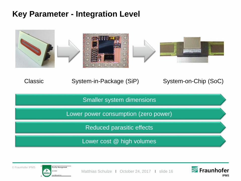
Key Parameter - Integration Level
Classic System-in-Package (SiP) System-on-Chip (SoC)
Smaller system dimensions
Lower power consumption (zero power)
Reduced parasitic effects
Lower cost @ high volumes

© Fraunhofer IPMS Matthias Schulze I October 24, 2017 I slide 17
MEMS-on-CMOS – Multi- Chip Heterogeneous Integration
Multi-chip solutions
Key features Parallel fabrication of CMOS/ ASICs and MEMS MEMS and CMOS designed, manufactured and tested independently MEMS manufacturing allow non-CMOS compatible processes (gold, copper, PZT) MEMS and CMOS connected via interposer using TSV technologies, ball grid arrays,
flip-chip or wire bonding
Combination of specific MEMS with commercially available standard ASIC simple, rapid and cost-efficient implementation Limited integration density
MEMS Chip
MEMS Chip

© Fraunhofer IPMS Matthias Schulze I October 24, 2017 I slide 18
MEMS-on-CMOS – Multi- Wafer Heterogeneous Integration
Merging MEMS and CMOS via wafer bonding – multi-wafer approach
Key features MEMS and CMOS/ASIC will be pre-fabricated on separate substrates Via formation during layer transfer (via-first) or after layer transfer (via-last) for establishing mechanical and/ or electrical contacts Via-first approach using metallic bond between two metal layers on separate wafers
(e.g. Al/Ge eutectic bond or Cu thermo-compressive bond) Via-last approach integrates contacts after bonding
Advantage:Integration of high performance materials (c-Si) and high temperature processes for MEMS wafers
Drawback:High alignment accuracy necessary, integration density limited and bond yield is still a critical issue
CMOS
MEMS

© Fraunhofer IPMS Matthias Schulze I October 24, 2017 I slide 19
MEMS-on-CMOS – Monolithic Integration
Can be performed as MEMS-first, interleaved and MEMS-last integration focus on MEMS-last integration
Applying bulk or surface micromachining after completion of CMOS/ IC Interconnection are realized using standard CMOS processes very high and reliable integration density
Substrate temperature during MEMS processing is limited to 450°C Integration in existing CMOS line possible, or MEMS will be integrated in specialized MEMS fab MEMS area shall fit to CMOS area
CMOS
MEMSAdvantage:Realization of rather complex MEMS MEMS/ MOEMS arrays
Drawback:450°C max. process temperatureMaterial limitation

© Fraunhofer IPMS Matthias Schulze I October 24, 2017 I slide 20
Outline
Short Intro Fraunhofer IPMS
MEMS-on-CMOS
MEMS Micro- Machining Technologies - Bulk and Surface Basics
Examples for Applications on CMOS Backplanes
Challenges and Solutions for MEMS-on-CMOS
Interaction with CMOS Fab
Integration of MEMS on CMOS Backplanes in MEMS Fab
Cu- wafer as a Special Case
Forschungsfabrik Mikroelektronik Deutschland – One Stop Shop
Summary

© Fraunhofer IPMS Matthias Schulze I October 24, 2017 I slide 21
Fabrication of sensors & actors out of the wafer’s material (bulk) itself
Bulk MEMS technologies for: MEMS scanning mirrors Pressure sensor Precision Silicon Components
2D- MEMS Scanner: rotational, resonant Pressure sensor Silicon component for spectrometer
Bulk MEMS Technology

© Fraunhofer IPMS Matthias Schulze I October 24, 2017 I slide 22
Fabrication of sensors & actors on wafer surface by using sacrificial layers
Surface MEMS technologies for: SLM: Spatial Light Modulator Micro- Bolometers CMUT: Capacitive Micro-machined Ultrasound Transducer
Surface MEMS Technology
Micro-Mirror-Arrays (SLM) Capacitive Micro-machined UT Micro-Bolometers

© Fraunhofer IPMS Matthias Schulze I October 24, 2017 I slide 23
Basic technology for resonant MEMS scanner Rotation: 1 & 2-dimensional Translation Quasi- static movement
Electrostatic driving principle In-Plane Comb-drive Resonant operation High deflection at low voltage Quasi-static through angular
pre-deflection (2nd wafer bonded)
Bulk MEMS Technology - MEMS Scanning Mirrors

© Fraunhofer IPMS Matthias Schulze I October 24, 2017 I slide 24
2nd Generation Spatial Light Modulator Multi- level architecture with separation of
mechanical parts from mirrors Actuator/ hinges: amorphous materials Mirror: Al- Alloy
Inorganic sacrificial layers
Hinge
Mirror
Surface MEMS Technology - Spatial Light Modulator
Characteristics of spatial light modulators Analogue deflection UV/DUV application (193/ 248nm) Planarity/ bow < 5nm @ 16µm mirror pitch
Integration of high reflectance mirrors Multilayer design for UV-VIS-NIR Using hybrid multilayer stacks
to reach sophisticated reflection
Electrode

© Fraunhofer IPMS Matthias Schulze I October 24, 2017 I slide 25
Surface MEMS Technology - CMUT
Principle of Capacitive Micro-machined Ultrasonic Transducer Cavity between two electrodes (wafer, top plate) Actuator plate deflected by electrostatic force and produce ultrasonic sound Sensor plate deflected by US wave change of capacity = measured signal
Technology Surface micromachining with sacrificial layer technology Closed or open CMUT, combined with PMUT MEMS-on-CMOS integration for arrays
CMUT
CMOS

© Fraunhofer IPMS Matthias Schulze I October 24, 2017 I slide 26
Fields of Application for CMUTs
Miniaturized & Scalable
Highly sensitive
Cost-efficient
Combination with ASIC
Material Analysis Gesture Control Fingerprint Medical Therapy Medical Imaging
[1] https://developer.apple.com/wwdc/ (19.05.17)[1] http://www.ndt.net/ndtaz/content.php?id=66 (08.06.2016)[2] https://phys.org/tags/hand%2Bgestures/sort/date/all/ (08.06.2016)[3] http://www.iphone-news.org/2014/01/28/apple-hat-viel-vor-mit-touch-id-52990/ (17.05.2017)[4] http://www2.isikun.edu.tr/personel/MustafaKaraman/mk_projects_files/image005.jpg[5] http://mhlhealth.com/images/Dermal_structure.png (17.05.17)
Infrasound Acoustic Ultrasound
animals and
chemistry
medical and non-
destructiveDiagnostics
20Hz 20kHz 2MHz 200MHz
Air Liquid Solid
1MHz 40MHz
Top plateopenings
Bottom plate Liquid-coupled CMUTAir-coupled CMUT
IPMS CMUT Range

© Fraunhofer IPMS Matthias Schulze I October 24, 2017 I slide 27
Combination of Bulk MEMS and Surface MEMS
Bulk MEMS for Mechanical structures Beam paths TSV / etc.
By intermediate filling and polishing enables further Surface MEMS
processing creating movable structures
Using aSi as sacrificial layer filled trenches can be released using XeF2
MEMS-on-CMOS too !
Alternative to backside processing

© Fraunhofer IPMS Matthias Schulze I October 24, 2017 I slide 28
Outline
Short Intro Fraunhofer IPMS
MEMS-on-CMOS
MEMS Micro- Machining Technologies - Bulk and Surface
Basics
Examples for Applications on CMOS Backplanes
Challenges and Solutions for MEMS-on-CMOS Interaction with CMOS Fab
Integration of MEMS on CMOS Backplanes in MEMS Fab
Cu- wafer as a Special Case
Forschungsfabrik Mikroelektronik Deutschland – One Stop Shop
Summary

© Fraunhofer IPMS Matthias Schulze I October 24, 2017 I slide 29
Why Using Foundry Processes for MEMS-on-CMOS?
Main Driver: Application specific functionalities Large variety in design features
(e.g. cell size, number of cells, voltage range, speed) Smaller feature size (e.g. micro-mirrors, bolometers …)
Use of Foundry CMOS processes allows High flexibility regarding CMOS nodes and PDKs Shorten time-to-market by: Separating MEMS from CMOS development and processing Final implementation of MEMS on external CMOS wafers
Interface between MEMS and CMOS Backplanebecomes the critical part

© Fraunhofer IPMS Matthias Schulze I October 24, 2017 I slide 30
How-to Start?
Design Comparison of PDK of different fabs (after NDA only) Discussion of interface between CMOS and MEMS Focus on one fab is maybe useful (especially for low volumes)
First wafers Costs for mask set + first wafer lot pretty high e.g. 150 k€/k$ for 180nm node
Recommended:Multi-project-wafer (MPW) runs for testing your design features several customers share costs for one mask set and lot MPW run contains basically 10mm² chip area, costs in the range
of 10 k€ and customer gets up to 50 diced samples Complete characterization of CMOS functionality in early project state
(speed, leakage currents, influences if you are close to fab’s design rules)

© Fraunhofer IPMS Matthias Schulze I October 24, 2017 I slide 31
Challenges Modifications of last interconnect/ ILD layers to realize an appropriate
interface for following MEMS processes Clarification of PCM test environment, depth of test structures and
possible arising contamination issues (typically done in BEoL) Tuning mix-and-match lithography to achieve high overlay accuracies Determine necessary actions to reach required in-chip surface topology,
especially for optical applications Additional chip design features when using sacrificial layer technology,
especially SiO2
Challenges for the Integration and Discussion with Fab
Discussion with fab about process adaptions Top layer SiO2 only (secure transport, further vias) PCM test only on few wafers (no further processing for tested) No additional frames between chips (all test structures inside chip layout) Bond pads shall not be opened

© Fraunhofer IPMS Matthias Schulze I October 24, 2017 I slide 32
Chip Topology – Initial Values after Foundry High surface inhomogeneity after CMOS processing due to interconnection
pattern/ fill factors are visible High difference between areas can be leveled-out using CMP Results are not satisfying with CMP only eventually it will lead to problems when applying homogeneous sacrificial layers
nm
+200nm SiO2CMP only
+400nm SiO2CMP only
nm nm
Initial stateafter fab

© Fraunhofer IPMS Matthias Schulze I October 24, 2017 I slide 33
Chip Topology – CMP + Inverse Mask
+200nm SiO2no inverse etch
+700nm SiO2-500nm inverse etching
Topology can be calculated from WLI (white light interferometry) This data was used to generate an inverse mask for height compensation height levels were transformed into different fill factors
Additional etch with inverse mask (+etch/CMP) can reduce surface inhomogeneity from ± 300nm to values less than ± 100nm
Necessary starting point for further (optical) MEMS processing with via opening
nm nm

© Fraunhofer IPMS Matthias Schulze I October 24, 2017 I slide 34
Chip Topology Chip topology is especially for optical MEMS a critical issue ! Large height differences between different chip areas inhomogeneous performance of subsequent CMP process steps (dishing) eventually to large spread in performance due to inhomogeneous sacrificial layer
Planarization of 1st sacrificial layer of wafers after different CMP/ inverse etch sequences

© Fraunhofer IPMS Matthias Schulze I October 24, 2017 I slide 35
Mix & Match Lithography
- Calculation ofcorrection-factors
- Rework- Illumination with
applied correct. factors
Property Unit Min. Mean. Max.OVL (X) nm -90,6 -22,0 56,1OVL (Y) nm 6,8 93,1 182,2
Property Unit Min. Mean. Max.OVL (X) nm -40,0 -4,0 24,0OVL (Y) nm -31,1 -0,1 28,5
Essential point to apply MEMS on CMOS wafers is to perform an accurate Mix & Match lithography with an overlay accuracy
Using i-line lithography an overlay measurement in combination with rework accuracy of approx. 50nm (stepper specs)
initial overlay corrected overlay

© Fraunhofer IPMS Matthias Schulze I October 24, 2017 I slide 36
Realizing Large MEMS Chips
MEMS feature may exceed maximum litho exposure field e.g. IPMS fabricates chips larger than 50mmx30mm
Need for complex litho stitching / partitioning
72 shots / chip ≈ 1600 shots / 200mm wafer ≈ 40min/wafer
Balance exposure time versus exposure accuracy to avoid drift effects andto achieve very good CD/OVL values
Adapt and control design features to minimize stitching effects
reticle layoutstitching chip

© Fraunhofer IPMS Matthias Schulze I October 24, 2017 I slide 37
Achieving Reliable Process Uniformity
Criticial litho features need tight process control (e.g. via CD-SEM)… e.g. mirror slits, hinges, holes, mass …
Example: hinge width with a target of 500nm
Hinge
Mirror
Electrode
500 ± 20nm
© Fraunhofer IPMS Matthias Schulze I October 24, 2017 I slide 38
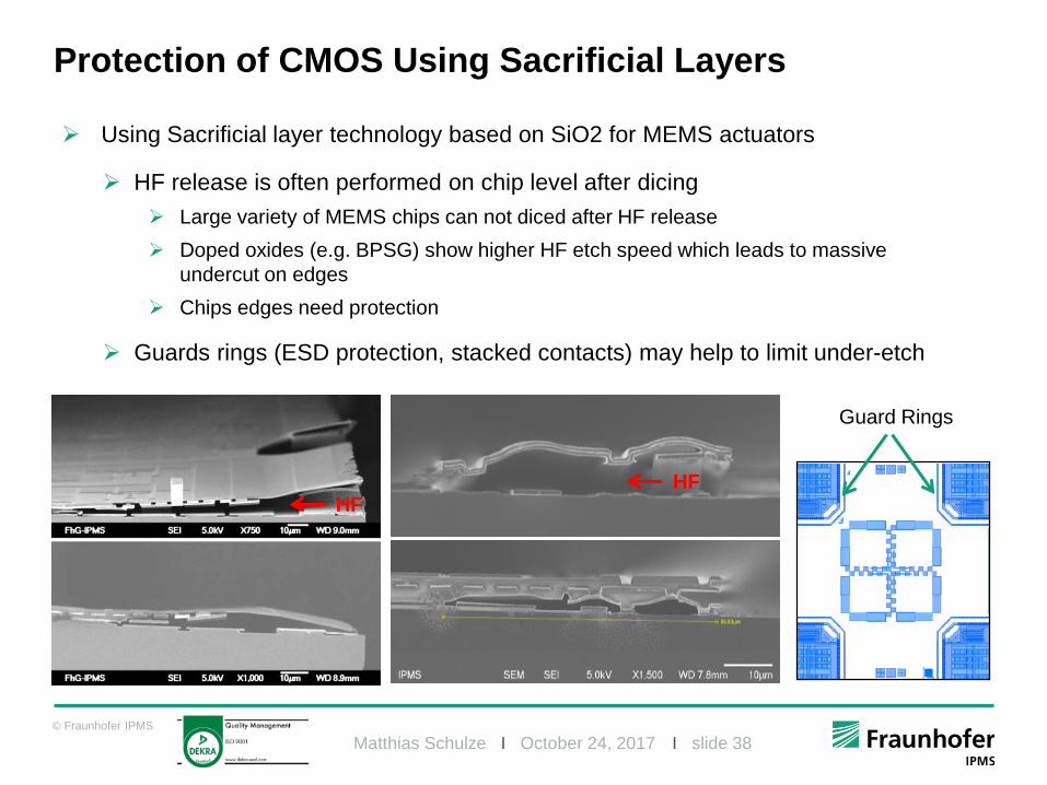
Protection of CMOS Using Sacrificial Layers
Guard Rings
Using Sacrificial layer technology based on SiO2 for MEMS actuators
HF release is often performed on chip level after dicing Large variety of MEMS chips can not diced after HF release Doped oxides (e.g. BPSG) show higher HF etch speed which leads to massive
undercut on edges Chips edges need protection
Guards rings (ESD protection, stacked contacts) may help to limit under-etch
HFHF

© Fraunhofer IPMS Matthias Schulze I October 24, 2017 I slide 39
Protection Ring after CMOS Processing
Define metal-free area (oxides only) Open trench close to chip frame Fill trench with aSi or other HF-inert material (e.g. Al2O3
from ALD + aSi) with good filling performance Pattern protection ring and planarize Continue with BEoL preparation Release sacrificial layers in MEMS part
Chip
Ring
30-50µm wide metal free ring
HF

© Fraunhofer IPMS Matthias Schulze I October 24, 2017 I slide 40
Preparing Copper Backplanes in a CMOS Cleanroom
Avoid mechanical damage:“open” copper due to mechanical damage of the wafer edge or arcing effects Wafers can not be processed further
SOI Wafer
Top Electrode
Leg
Last metalAlCuVery copper-rich AlCu
Nitride/ Al2O3-Sealing200nm Al2O3
Last metal copper free (AlCu)Diffusion of copper from layers below into the AlCu Additional risk for Cu-
contamination of the CMOS/ MEMS line
Look at diffusion of Copper:

© Fraunhofer IPMS Matthias Schulze I October 24, 2017 I slide 41
Outline
Short Intro Fraunhofer IPMS
MEMS-on-CMOS
MEMS Micro- Machining Technologies - Bulk and Surface
Basics
Examples for Applications on CMOS Backplanes
Challenges and Solutions for MEMS-on-CMOS
Interaction with CMOS Fab
Integration of MEMS on CMOS Backplanes in MEMS Fab
Cu- wafer as a Special Case
Forschungsfabrik Mikroelektronik Deutschland – One Stop Shop
Summary

© Fraunhofer IPMS Matthias Schulze I October 24, 2017 I slide 42
Freiburg
DresdenDuisburg
Erlangen
Itzehoe
Berlin
Chemnitz
München
2
71
946
10
118 12
Fürth/Nürnberg
4 5
Wachtberg3
13
12
3
5
6
9
78
1011
4
12
13
4
Ilmenau4
Angewandte Festkörperphysik IAFElektronische Nanosysteme ENASHochfrequenzphysik und Radartechnik FHRIntegrierte Schaltungen IISIntegrierte Systeme und Bauelementetechnologie IISBMikroelektronische Schaltungen und Systeme IMSModulare Festkörper-Technologien EMFTNachrichtentechnik, Heinrich-Hertz-Institut HHIPhotonische Mikrosysteme IPMSSiliziumtechnologie ISITZuverlässigkeit und Mikrointegration IZMFerdinand-Braun Institut - Leibniz-Institut für Höchstfrequenztechnik FBHLeibniz-Institut für Innovative Mikroelektronik IHP
13 Fraunhofer and 2 Leibniz Institutes Joining Their Forces
Investment of 350 Mill. Euro in infrastructure One-stop-shop for our customers

© Fraunhofer IPMS Matthias Schulze I October 24, 2017 I slide 43
Technology Key Area 1Investment: 141 Mill. Euro
Cutting- Edge silicon based technologies forsensors, actuators and information technology
Technology Key Area 2Investment: 73 Mill. Euro
Compound semiconductors with new materials for energy saving and communications
Technology Key Area 3 Investments: 43 Mill. Euro
Hetero-Integration – novel combinations of silicon with other semiconductors
Technology Key Area 4Investment: 84 Mill. Euro
Design, test and reliability
FMD – Setup – Four Technology Key Areas

© Fraunhofer IPMS Matthias Schulze I October 24, 2017 I slide 44
What does it mean for IPMS (200mm MEMS)?
IPMS will strengthen its MEMS-on-CMOS capabilities and competence in mirror technologies with key investments in: PVD tools for high performance mirrors
(hybrid layer stacks containing dielectrics and metals) Etch tools for patterning of hybrid multilayers In-line high precision reflectometer Anti- stiction tool to improve performance of digital actuators 200/300mm DUV lithography with 130nm L/S
(scanner, tracks, overlay) PVD tool for development of new sensor materials (co-sputtering)
Tailored solutions in co-operation with all FMD members Monolithic and heterogeneous MEMS-on-CMOS integration with smaller
feature sizes New assembly solutions (e.g. TSV, interposer, hermetic sealing) Push in development of new MEMS materials and driving concepts
© Fraunhofer IPMS Matthias Schulze I October 24, 2017 I slide 45
Outline
Short Intro Fraunhofer IPMS
MEMS-on-CMOS
MEMS Micro- Machining Technologies - Bulk and Surface
Basics
Examples for Applications on CMOS Backplanes
Challenges and Solutions for MEMS-on-CMOS
Interaction with CMOS Fab
Integration of MEMS on CMOS Backplanes in MEMS Fab
Cu- wafer as a Special Case
FMD – One Stop Shop
Summary
© Fraunhofer IPMS Matthias Schulze I October 24, 2017 I slide 46
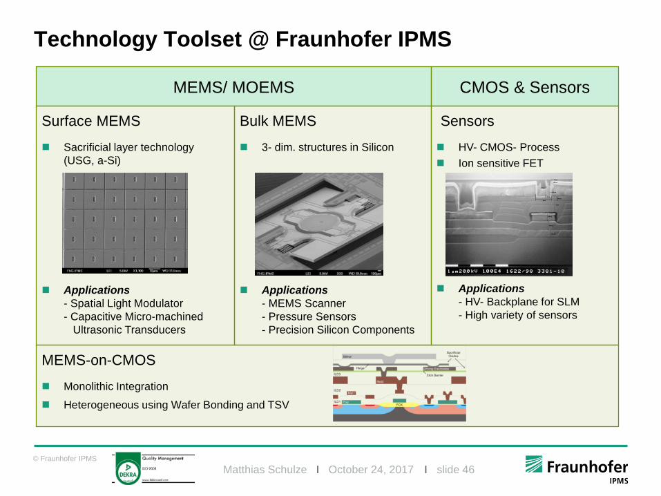
Technology Toolset @ Fraunhofer IPMS
Surface MEMS
Sacrificial layer technology (USG, a-Si)
Applications- Spatial Light Modulator- Capacitive Micro-machined
Ultrasonic Transducers
Bulk MEMS
3- dim. structures in Silicon
Applications- MEMS Scanner- Pressure Sensors- Precision Silicon Components
Sensors
HV- CMOS- Process Ion sensitive FET
Applications- HV- Backplane for SLM- High variety of sensors
CMOS & SensorsMEMS/ MOEMS
MEMS-on-CMOS
Monolithic Integration Heterogeneous using Wafer Bonding and TSV

© Fraunhofer IPMS Matthias Schulze I October 24, 2017 I slide 47
IPMS – CMOS compatible 200mm MEMS Line
Specific MEMS Equipment
i-line Stepper, Mask Alignerwith Spin and Spray Coaters
HT Furnace and Annealing
LP- and PE-CVD (USG, BPSG, SA-USG, HDP-oxide, a-Si, nitride)
Multiple Sputtering Tools (interconnects, mirrors, dielectrics)
ALD of Al2O3/ SiO2/ HfO2
TMAH wet etch
Dry etch tools for deep Si, dielectrics and metals
CMP process (5-zone)
Release Etch for SiO2 and Si sacrificial layers
High and low temperature fusion bonding
Large variety of testing equipment
Deep Si etch comb drives
Isolated tenchesUpper edge of a groove in Si (etched with TMAH)
Spray coated resist, 4 µm
10 µm
Lithography in deep structures
Deep Si Etch for membranes
a-Si on metal line after CMP Inorganic Release (USG with vHF)

© Fraunhofer IPMS Matthias Schulze I October 24, 2017 I slide 48
THANK YOU FOR YOUR KIND ATTENTION!
Matthias Schulze – Head of Engineering Departmentphone: +49-351-8823-335 email: [email protected]://www.ipms.fraunhofer.de/en/mems-foundry