
Wearable, 16-phase multi-sensor SpO2 and HRM ref design ...
61
CC2640R2F AFE4420 (Integrated AFE for PPG) VDDS2/3 RF VDDS TX_SUP RX_SUP IO_SUP TPS61099 (Boost) TPS63036 (Buck-Boost) LC Filter 4.2 V 2.1 V* 2.1 V 1.8 V to 3 V (from Coin-cell Battery) 1.8 V to 3 V (Directly from the Battery) Data Log Memory RESET LEDs: BLE Status Low-Battery Indication TIDA-010029 LED_TX PD_RX Sensor Board (PPG) *Internal LDO for AFE4420 is enabled JTAG Connection MCU SPI / I2C 2.1 V TPD1E10B06 x 7 TPD1E10B06 x 5 1 TIDUEG6A – October 2018 – Revised March 2019 Submit Documentation Feedback Copyright © 2018–2019, Texas Instruments Incorporated Wearable, 16-phase multi-sensor SpO2 and heart rate monitor (HRM) reference design with Bluetooth ® 5 Design Guide: TIDA-010029 Wearable, 16-phase multi-sensor SpO2 and heart rate monitor (HRM) reference design with Bluetooth ® 5 Description This reference design enables a wearable, optimized saturation of peripheral capillary oxygen (SpO2) and multi-sensor, multi-wavelength optical heart rate monitor (HRM). It uses the AFE4420 device, which is a single-chip, bio-sensing front end for photoplethysmography (PPG) measurements. It supports up to four switching light-emitting diodes (LEDs) and up to four photodiodes to enable signal acquisition of up to 16 phases. The CC2640R2F device (supporting Bluetooth ® low energy 4.2 and 5) transfers the measured data to a remote location. This patient-monitoring design uses a single CR3032 battery with a 30-day life cycle. Raw data is available to calculate heart rate, SpO2, and other related parameters. 2 onboard light-emitting diodes (LEDs) identify low-battery detection and a Bluetooth connection. Resources TIDA-010029 Design Folder AFE4420 Product Folder CC2640R2F Product Folder TPS61099 Product Folder TPS63036 Product Folder TPD1E10B06 Product Folder ASK Our E2E™ Experts Features • Provides raw data to calculate heart rate, SpO2, and other related parameters • Uses single-chip, bio-sensing, front-end AFE4420 device for PPG measurement – Supports up to 4 LEDs and 4 photodiodes with ambient subtraction to improve signal-to-noise ratio (SNR) – Enables signal acquisition of up to 16 phases and multi-wavelength measurements with the flexible allocation of LEDs and photodiodes in each phase • Integrated Arm ® Cortex ® -M3 and 2.4-GHz RF transceiver (CC2640R2F) supports wireless data transfer through Bluetooth ® low energy 4.2 and 5.0 • Operates from CR3032 (3-V, 500-mA coin cell battery) with a battery life of 30 days using highly efficient DC/DC converters • Small form factor helps in easy adaptation to wearable applications Applications • Pulse oximeter • Wearable fitness and activity monitor • Multiparameter patient monitor • Medical sensor patches An IMPORTANT NOTICE at the end of this TI reference design addresses authorized use, intellectual property matters and other important disclaimers and information.
Transcript of Wearable, 16-phase multi-sensor SpO2 and HRM ref design ...

CC2640R2FAFE4420(Integrated AFE for PPG)
VDDS2/3
RF
VDDSTX_SUP RX_SUP
IO_SUP
TPS61099(Boost)
TPS63036(Buck-Boost)
LC Filter
4.2 V 2.1 V* 2.1 V
1.8 V to 3 V(from Coin-cell Battery)
1.8 V to 3 V (Directly from the Battery)
Data Log Memory
RESET
LEDs:BLE StatusLow-Battery Indication
TIDA-010029
LED_TX
PD_RX
Sensor Board (PPG)
*Internal LDO for AFE4420 is enabled
JTAG Connection
MCU
SPI / I2C
2.1 V
TP
D1E
10B
06 x
7
TP
D1E
10B
06 x
5
1TIDUEG6A–October 2018–Revised March 2019Submit Documentation Feedback
Copyright © 2018–2019, Texas Instruments Incorporated
Wearable, 16-phase multi-sensor SpO2 and heart rate monitor (HRM)reference design with Bluetooth® 5
Design Guide: TIDA-010029Wearable, 16-phase multi-sensor SpO2 and heart ratemonitor (HRM) reference design with Bluetooth® 5
DescriptionThis reference design enables a wearable, optimizedsaturation of peripheral capillary oxygen (SpO2) andmulti-sensor, multi-wavelength optical heart ratemonitor (HRM). It uses the AFE4420 device, which is asingle-chip, bio-sensing front end forphotoplethysmography (PPG) measurements. Itsupports up to four switching light-emitting diodes(LEDs) and up to four photodiodes to enable signalacquisition of up to 16 phases. The CC2640R2Fdevice (supporting Bluetooth® low energy 4.2 and 5)transfers the measured data to a remote location. Thispatient-monitoring design uses a single CR3032battery with a 30-day life cycle. Raw data is availableto calculate heart rate, SpO2, and other relatedparameters. 2 onboard light-emitting diodes (LEDs)identify low-battery detection and a Bluetoothconnection.
Resources
TIDA-010029 Design FolderAFE4420 Product FolderCC2640R2F Product FolderTPS61099 Product FolderTPS63036 Product FolderTPD1E10B06 Product Folder
ASK Our E2E™ Experts
Features• Provides raw data to calculate heart rate, SpO2,
and other related parameters• Uses single-chip, bio-sensing, front-end AFE4420
device for PPG measurement– Supports up to 4 LEDs and 4 photodiodes with
ambient subtraction to improve signal-to-noiseratio (SNR)
– Enables signal acquisition of up to 16 phasesand multi-wavelength measurements with theflexible allocation of LEDs and photodiodes ineach phase
• Integrated Arm® Cortex®-M3 and 2.4-GHz RFtransceiver (CC2640R2F) supports wireless datatransfer through Bluetooth® low energy 4.2 and 5.0
• Operates from CR3032 (3-V, 500-mA coin cellbattery) with a battery life of 30 days using highlyefficient DC/DC converters
• Small form factor helps in easy adaptation towearable applications
Applications• Pulse oximeter• Wearable fitness and activity monitor• Multiparameter patient monitor• Medical sensor patches
An IMPORTANT NOTICE at the end of this TI reference design addresses authorized use, intellectual property matters and otherimportant disclaimers and information.
� �%Sp02 110 25 R � u
ACrms of RedDC of Red
RACrms of IR
DC of IR
System Description www.ti.com
2 TIDUEG6A–October 2018–Revised March 2019Submit Documentation Feedback
Copyright © 2018–2019, Texas Instruments Incorporated
Wearable, 16-phase multi-sensor SpO2 and heart rate monitor (HRM)reference design with Bluetooth® 5
1 System Description
1.1 Introduction to Parameters Measured Using TIDA-010029The TIDA-010029 device can be used to measure the following parameters: photoplethysmography(PPG), heart-rate monitoring (HRM), and peripheral capillary oxygen saturation (SpO2).
PPG is an optical measurement of the volume of an organ. In principle, PPG illuminates the skin andsubcutaneous tissue with light of a specific wavelength from a light-emitting diode (LED) to measure organvolume. This light is absorbed, passed through, or reflected back. A photodiode sensor measures the lightthat is either transmitted or reflected, depending on where it is placed relative to the LED. The light is thenconverted to an electrical signal. The information can be used to determine the heart rate of a person.PPG also provides more information about blood flow and blood pressure. This measurement can beconducted at various locations on the body to examine the blood flow to different regions. When measuredclosest to the aorta of the heart (for example, the left arm), some additional information can be gainedregarding the cardiac output and heart valve function. One advantage that PPG has is the number of skincontacts which are required to measure it. Because PPG can be determined from reflected or transmittedlight, only a single point of contact is necessary to measure it. This feature allows for easy, continuoustime measurements, which is the most attractive advantage to wearable electronics such as fitnesstrackers.
Mostly green LEDs are used for measuring heart rates. A green LED has often been used in the reflectivesensor to extract the PPG signal. Due to its wavelength, green light is known to penetrate the tissue lessthan higher wavelength LEDs. Hence, more unabsorbed, or reflected, light comes out of the tissue withgreen than with other colors. Sensing the green light from more than one powered device (PD) oreliminating from more than one LED surrounding the PD helps.
Red and infrared (IR) lights are used for pulse oximetry to estimate the true hemoglobin oxygen saturationof arterial blood. Oxyhemoglobin (HbO2) absorbs visible and infrared light differently thandeoxyhemoglobin (Hb) and appears bright red as opposed to the darker brown of Hb. Absorption in thearterial blood is represented by an AC signal that is superimposed on a DC signal, representingabsorptions in other substances like pigmentation in tissue, venous, capillary, bone, and so forth. Thecardiac-synchronized AC signal is approximately 1% of the DC level. This value is referred to as theperfusion index percentage. Equation 1 approximates the ratio of ratios, R, and percent SpO2 as follows:
(1)
Equation 2 gives the standard model of computing SpO2. This model is often used in this literature in thecontext of medical devices. However, accurate percentage of SpO2 is computed based on the empiricalcalibration of the ratio of ratios for the specific device.
(2)

wavelength (nm)
G (
mm
)
400 500 600 700 800 900 10000.5
1
1.5
2
2.5
3
D001
infraredorangegreenblue
www.ti.com System Description
3TIDUEG6A–October 2018–Revised March 2019Submit Documentation Feedback
Copyright © 2018–2019, Texas Instruments Incorporated
Wearable, 16-phase multi-sensor SpO2 and heart rate monitor (HRM)reference design with Bluetooth® 5
The reliability of PPG signals measured during normal daily life can be reduced by motion artifacts. Thus,various techniques for the robust measurement of PPG signals during motion have been researched. Oneapproach, based on the optical characteristics of tissue, can be the choice of light wavelength. The lightsources used with PPG have been chosen at various wavelengths including the near-infrared (NIR) (forexample, 810 or 940 nm), red, green, and blue. NIR and red wavelengths are generally used in PPGresearch and for routine clinical applications. However, among the possible light colors, green light PPGhas been shown to have the least influence from motion artifacts when compared with the NIR light PPG.In fact, green light PPG is now often used in smartphone heart rate (HR) measurement, which is availablenot only in the laboratory but also during normal daily life. Naturally, the influences of artifacts on the PPGsignal are related to the wavelength of the light source simply because of the wavelength dependence ofthe light absorption (for example, water, melanin, oxy- and deoxyhemoglobin) and therefore thepenetration depth into the tissue. The additional wavelengths can also be used to distinguish theabsorption of deoxyhemoglobin (RHb) and oxyhemoglobin (HbO2). More details are available in Section 6(Reference 6) and Figure 1.
Figure 1. Optical Penetration Depth δ Shown for a Range of Light Sources of Different Wavelengths

System Description www.ti.com
4 TIDUEG6A–October 2018–Revised March 2019Submit Documentation Feedback
Copyright © 2018–2019, Texas Instruments Incorporated
Wearable, 16-phase multi-sensor SpO2 and heart rate monitor (HRM)reference design with Bluetooth® 5
1.2 Typical Applications• Wireless Patient Monitor: Wireless patient monitors measure vital signs and send data across to a
remote location through wireless technology (Bluetooth®, Bluetooth® low energy, Wi-Fi®, Sub 1-GHz orNFC/RFID). These monitors are typically battery-powered and have low operating currents to work forlonger battery life. The solutions are notably compact, unlike multiparameter bedside monitors.
• Medical Sensor Patches: Medical sensor patches are wearable, battery-operated patient monitorswhich can be stuck on the human body for measurement of different parameters like ECG,temperature, blood pressure, and so forth.
• Pulse Oximeter: The pulse oximeter measures blood oxygenation by sensing the IR and red-lightabsorption properties of deoxygenated and oxygenated hemoglobin. The oximeter is comprised of asensing probe that attaches to the ear lobe, toe, or finger of a patient and is connected to a dataacquisition system for calculation and display of the oxygen saturation level, heart rate, and blood flow.Light sources, typically LEDs, shine visible red and IR light. Deoxygenated hemoglobin allows moreinfrared light to pass through and absorb more red light. Highly oxygenated hemoglobin allows morered light to pass through and absorbs more IR light. The oximeter senses and calculates the amount oflight at those wavelengths proportional to the oxygen saturation (or desaturation) of the hemoglobin.The use of light in the absorbency measurement requires the designer to have a true light-to-voltageconversion using current as the input signal.
• Wearable Fitness and Activity Monitor: Fitness monitors measure both the amount and rate of exerciseof a person (for example, miles and pace run) as well as effort expended (for example, throughmonitoring heart rate). Typically, a wristwatch or wrist-worn display is used for control and providingfeedback. Stored data can be downloaded to a computer through a USB or wireless USB dongle. Allparts of the system require ultra-low power, embedded controllers and low-power RF forcommunication. Heart-rate monitoring and exercise-output monitoring (for example, a running pacesensor or power sensor) require additional signal conditioning.
• Multiparameter Patient Monitor: Multiparameter patient monitors measure vital signs and send acrossto a remote location through wired or wireless technology (Bluetooth®, Bluetooth® low energy, Wi-Fi®,Sub 1-GHz or NFC/RFID) or to a local storage. These monitors have different modules to measuredifferent vital signs.
• Other adjacent applications which can use multi-wavelength optical measurement are food analyzers,air particle analyzers, and air purifiers.

www.ti.com System Description
5TIDUEG6A–October 2018–Revised March 2019Submit Documentation Feedback
Copyright © 2018–2019, Texas Instruments Incorporated
Wearable, 16-phase multi-sensor SpO2 and heart rate monitor (HRM)reference design with Bluetooth® 5
1.3 System Specifications and Design FeaturesThe TIDA-010029 reference design is a wearable patient monitor and has the following features:• Simple, wearable, PPG measurement design that provides raw data to calculate heart rate, SpO2, and
other related parameters• Single-chip, bio-sensing, front end for high-resolution PPG measurements (AFE4420 device)
– Only device on the market with this level of integration, low power, size, and flexibility– Supports 4 LEDs and 4 PDs with digital ambient subtraction to improve the signal-to-noise ratio
(SNR)– Flexibility of ultra-low-power modes and integrated FIFO can keep the MCU in sleep mode to
increase the battery operation time– Signal acquisition of up to 16 phases and flexible allocation of LEDs and PDs in each phase enable
multi-wavelength measurements• Wireless data transfer supporting Bluetooth low energy 4.2 and 5.0
– Integrated Arm Cortex-M3 and 2.4-GHz RF transceiver (CC2640R2F device)– Internal DC/DC converter helps improve the overall efficiency– Built-in, low-battery detection algorithm helps reduce the external components– Better routing in small form factor (all digital peripheral pins can be routed to any general-purpose
input/output (GPIO)• Operated from CR3032 (3-V, 500-mA coin-cell battery), which offers 100 hours of continuous operation• Low-power (battery life of 30 days for 1 second/minute transmission)• Can also be operated using CR2032 (3-V, 225-mA coin cell battery) with reduced operating time• Plug-in board approach enables easy adaptation to custom PPG sensors
1.4 Key System SpecificationsTable 1 lists the different characteristics and specifications of the TIDA-010029 board.
Table 1. Key System Specifications and Capabilities
CHARACTERISTICS SPECIFICATIONSInput voltage (VIN) 1.8 V to 3 V (coin-cell CR3032 battery)
TX_SUP 4.2 VRX_SUP 2.1 VIO_SUP 2.1 V
Number of LEDs for PPG measurement Three (green, red, and IR)Number of photodiodes for PPG measurement Two (for SFH7072)
External memory Supported, but not populated onboard
LED indicationsLow-battery flag
Bluetooth low energy (BLE) statusCommunication SPI
Interface to controller 8-pin connector (100 mil, part number PRPC008SADN-RC)Board dimension (main board) 75 mm x 50 mm
Board dimension (sensor board) 28 mm x 28 mm

CC2640R2FAFE4420(Integrated AFE for PPG)
VDDS2/3
RF
VDDSTX_SUP RX_SUP
IO_SUP
TPS61099(Boost)
TPS63036(Buck-Boost)
LC Filter
4.2 V 2.1 V* 2.1 V
1.8 V to 3 V(from Coin-cell Battery)
1.8 V to 3 V (Directly from the Battery)
Data Log Memory
RESET
LEDs:BLE StatusLow-Battery Indication
TIDA-010029
LED_TX
PD_RX
Sensor Board (PPG)
*Internal LDO for AFE4420 is enabled
JTAG Connection
MCU
SPI / I2C
2.1 V
TP
D1E
10B
06 x
7
TP
D1E
10B
06 x
5
System Overview www.ti.com
6 TIDUEG6A–October 2018–Revised March 2019Submit Documentation Feedback
Copyright © 2018–2019, Texas Instruments Incorporated
Wearable, 16-phase multi-sensor SpO2 and heart rate monitor (HRM)reference design with Bluetooth® 5
2 System Overview
2.1 Block DiagramFigure 2 shows the high-level block diagram for the TIDA-010029 device, which is a simple, wearable,optical heart-rate and SpO2 monitor. The AFE4420 is a single-chip, bio-sensing, front end for PPGmeasurements. The AFE4420 device can drive up to 4 LEDs and support receive signal chains for up to 4photodiodes. The flexible allocation of LEDs and PDs in each phase can enable multi-wavelengthmeasurements. The AFE4420 device communicates with the CC2640R2F device over serial peripheralinterface (SPI), or I2C. The CC2640R2F is a microcontroller with an integrated Arm® Cortex®-M3 and 2.4-GHz RF transceiver. The design supports wired data capture using a JTAG connection, as well aswireless data capture by sending it over Bluetooth® low enegery (BLE) through the antenna.
The board is powered using a 3-V, 500-mA coin-cell battery, CR3032. A boost converter (TPS61099)powers TX_SUP for the AFE4420 device, which supports the internal LED drivers for PPG measurement.A buck-boost converter (TPS63036) powers RX_SUP and IO_SUP for the AFE4420 device and VDDS2and VDDS3 for the CC2640R2F device. VDDS for the CC2640R2F device is directly powered by thebattery.
The board supports connections to external data-log memory, but it is currently not populated. The boardindicates battery power source availability, low-battery detection, Bluetooth low energy connection status,and lead-off detection through onboard LEDs.
All the connections from the main to the external world are protected by electrostatic discharge (ESD)diodes (TPD1E10B06). The design contains a main board and a sensor board.
Figure 2. TIDA-010029 Block Diagram

www.ti.com System Overview
7TIDUEG6A–October 2018–Revised March 2019Submit Documentation Feedback
Copyright © 2018–2019, Texas Instruments Incorporated
Wearable, 16-phase multi-sensor SpO2 and heart rate monitor (HRM)reference design with Bluetooth® 5
2.2 Highlighted ProductsKey features of the highlighted devices are mentioned in the following sections.
2.2.1 AFE4420The AFE4420 device is an analog front-end (AFE) for PPG signal acquisition. The device can also beused for optical bio-sensing applications, such as heart-rate monitoring (HRM) and SpO2. The PPG signalchain supports up to 4 switching LEDs and up to 4 PDs. The LEDs can be switched on using a fully-integrated LED driver. The current from the PD is converted into voltage by the trans-impedance amplifier(TIA) and digitized using an analog-to-digital converter (ADC). The ADC codes from the PPG phases canbe stored in a 128-sample first in, first out (FIFO) block and read out using either an I2C or SPI.
2.2.2 CC2640R2FThe CC2640R2F device is a wireless MCU targeting Bluetooth® low energy 4.2 and 5 applications. Thedevice is a member of the SimpleLink™ ultra-low-power CC26xx family of cost-effective, 2.4-GHz RFdevices. Low active RF and MCU current and low-power mode current consumption provide excellentbattery lifetime and allow for operation on small coin-cell batteries and in energy-harvesting applications.The SimpleLink Bluetooth low energy CC2640R2F device contains a 32-bit Arm Cortex-M3 core, whichruns at 48 MHz as the main processor and a rich peripheral feature set, which includes a unique ultra-lowpower sensor controller. This sensor controller is ideal for interfacing external sensors and for collectinganalog and digital data autonomously while the rest of the system is in sleep mode. Thus, the CC2640R2Fdevice is great for a wide range of applications where long battery lifetime, small form factor, and ease ofuse are important. The power and clock management and radio systems of the CC2640R2F wirelessMCU require specific configuration and handling by software, which has been implemented in the TI-RTOS, to operate correctly.
2.2.3 TPS61099The TPS61099 boost converter uses a hysteretic control topology to obtain maximum efficiency at minimalquiescent current. The TPS61099 device only consumes 1-μA quiescent current under a light loadcondition and can achieve up to 75% efficiency at a 10-μA load with a fixed output voltage version. TheTPS61099 device can also support up to 300-mA output current from 3.3 V to 5 V conversion and achieveup to 93% at a 200-mA load. The TPS61099 device also offers both Down Mode and Pass-Throughoperations for different applications. In Down Mode, the output voltage can still be regulated at a targetvalue even when the input voltage is higher than the output voltage. In Pass-Through Mode, the outputvoltage follows the input voltage. The TPS61099x device exits Down Mode and enters into Pass-ThroughMode when VIN > VOUT + 0.3 V. The TPS61099x device supports true shutdown function when it isdisabled, which disconnects the load from the input supply to reduce the current consumption. TheTPS61099x device offers both an adjustable output voltage version and fixed output voltage version. TheTPS61099x device is available in a 6-ball, 1.23-mm × 0.88-mm, WCSP package.
2.2.4 TPS63036The TPS63036 is a noninverting, buck-boost converter capable of providing a regulated output voltagefrom an input supply that can be higher or lower than the output voltage. The buck-boost converter isbased on a fixed-frequency, pulse width modulation (PWM) controller, which uses synchronousrectification to obtain maximum efficiency. At low-load currents, the converter enters a power-save modeto maintain high efficiency over a wide-load current range. The power save mode can be disabled, forcingthe converter to operate at a fixed switching frequency. The maximum average current in the switches islimited to a typical value of 1000 mA. The output voltage is programmable using an external resistordivider. The converter can be disabled to minimize battery drain.
2.2.5 TPD1E10B06The TPD1E10B06 device is a single-channel, electrostatic discharge (ESD), transient voltage suppression(TVS) diode in a small 0402 package. This TVS protection product offers ±30-kV contact ESD, ±30-kVIEC air-gap protection, and an ESD clamp circuit, with a back-to-back TVS diode for bipolar orbidirectional signal support. The 0402 package is an industry standard and is convenient for componentplacement in space-saving applications.

System Overview www.ti.com
8 TIDUEG6A–October 2018–Revised March 2019Submit Documentation Feedback
Copyright © 2018–2019, Texas Instruments Incorporated
Wearable, 16-phase multi-sensor SpO2 and heart rate monitor (HRM)reference design with Bluetooth® 5
NOTE: The CC2642R device is a new and small wireless MCU device targeting Bluetooth® 4 and 5low energy applications. The CC2642R1FRGZ device is pin-compatible with theCC2640R2FRGZR device.

www.ti.com System Overview
9TIDUEG6A–October 2018–Revised March 2019Submit Documentation Feedback
Copyright © 2018–2019, Texas Instruments Incorporated
Wearable, 16-phase multi-sensor SpO2 and heart rate monitor (HRM)reference design with Bluetooth® 5
2.3 System Design Theory and Design ConsiderationsThis section explains the design theory for each of the devices used in the design.
2.3.1 AFE4420 and Power SupplyFigure 3 shows different connections for the AFE4420 device.
The AFE4420 device needs three power supplies: TX_SUP, RX_SUP, and IO_SUP. TX_SUP (4.2 V) isgenerated using the TPS61099 device. RX_SUP (2.1 V) is generated using the TPS63036 device.IO_SUP is the same as RX_SUP.
For PPG measurement, the LEDs are driven using the TX2, TX3, and TX4 pins (TX1 is not connected inthe design). The reflected signals are detected using PDs connected to the INP-INM and INP2-INM2 pins(INP3-INM3 and INP4-INM4 pins are not connected in the design).
The BG pin is connected to the internal bandgap voltage. The BG pin is decoupled using a 0.1-µFcapacitor (C11) on the board.
Figure 3. AFE4420 Connections Schematic
For the AFE4420 device, RX_SUP is filtered using an LC filter consisting of the ferrite bead L1 andcapacitors C6 and C7.

System Overview www.ti.com
10 TIDUEG6A–October 2018–Revised March 2019Submit Documentation Feedback
Copyright © 2018–2019, Texas Instruments Incorporated
Wearable, 16-phase multi-sensor SpO2 and heart rate monitor (HRM)reference design with Bluetooth® 5
Table 2 lists the connections between the AFE4420 and CC2640R2F devices.
Table 2. Connections Between AFE4420 and CC2640R2F
AFE4420 PINNUMBER FUNCTION CC2640R2F PIN
NUMBER FUNCTION COMMENTS
E1 /RESET 6 DIO_1 Reset for the AFE
A4 I2C_SPI_SEL N/A N/A
Selection between SPI and I2C. Forthis design, SPI is selected, so thispin is connected to RX_SUP througha 0-Ω resistor (R2).
F3 I2C_CLK 16 DIO_10 SPI_CLKF2 I2C_DAT 14 DIO_8 SPI_INE2 SDOUT 15 DIO_9 SPI_OUTE3 SEN 5 DIO_0 AFE_SPI_END3 GPIO1 21 DIO_15 Extra GPIOF4 ADC_RDY 28 DIO_18 ADC ready signalF1 CLK 29 DIO_19 AFE clock
B4 CONTROL1 N/A N/A
Enables or disables the internal LDO.For this design, the internal LDO isenabled, so this pin is connected toGND through a 0-Ω resistor (R4).
2.3.2 CC2640R2F MicrocontrollerFigure 4 shows the schematic for configuring the CC2640R2F MCU.
Figure 4. CC2640R2F MCU Schematic
The VDSS power supply for the MCU, 2.1 V, is derived using the TPS63036 device. The VDDR powersupply is generated using the internal DC/DC of the CC2640R2F MCU, and L8, C20, C25, and C27 formthe filter components for the same. Y1 is the 24-MHz, high-frequency external clock, and Y2 is the 32-kHz,low-frequency external clock. The GPIO pins of the CC2640R2F MCU (DIO_0 to DIO_30) interface withdifferent functions such as memory interface lines, AFE4420 interface lines, SPI communication, LEDdrives, and so forth.
The RF front end is used in differential-ended configurations with internal biasing. A balunLFB182G45BG5D920 device is used for the RF front end and tuned for application. J7 is a connector forconducted RF measurements, if required. The antenna is a PCB antenna.
www.ti.com System Overview
11TIDUEG6A–October 2018–Revised March 2019Submit Documentation Feedback
Copyright © 2018–2019, Texas Instruments Incorporated
Wearable, 16-phase multi-sensor SpO2 and heart rate monitor (HRM)reference design with Bluetooth® 5
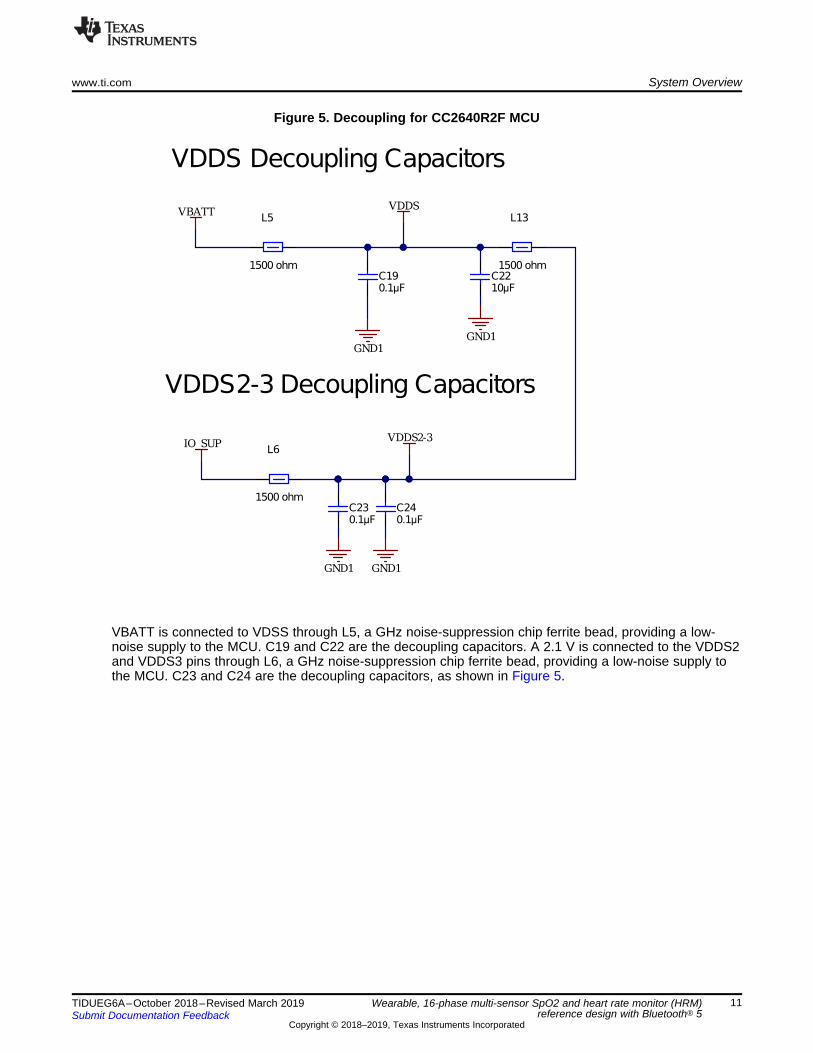
Figure 5. Decoupling for CC2640R2F MCU
VBATT is connected to VDSS through L5, a GHz noise-suppression chip ferrite bead, providing a low-noise supply to the MCU. C19 and C22 are the decoupling capacitors. A 2.1 V is connected to the VDDS2and VDDS3 pins through L6, a GHz noise-suppression chip ferrite bead, providing a low-noise supply tothe MCU. C23 and C24 are the decoupling capacitors, as shown in Figure 5.

System Overview www.ti.com
12 TIDUEG6A–October 2018–Revised March 2019Submit Documentation Feedback
Copyright © 2018–2019, Texas Instruments Incorporated
Wearable, 16-phase multi-sensor SpO2 and heart rate monitor (HRM) referencedesign with Bluetooth® 5
Figure 6. MCU Programming Connector
The MCU is programmed using a JTAG connection, as shown in Figure 6. The connector inputs areprotected by ESD diodes (TPD1E10B06DPYR) from Texas Instruments. The TPD1E10B06 device is asingle-channel, ESD, TVS diode in a small 0402 package. This TVS protection product offers ±30-kVcontact ESD, ±30-kV IEC air-gap protection, and an ESD clamp circuit with a back-to-back TVS diode forbipolar or bidirectional signal support.
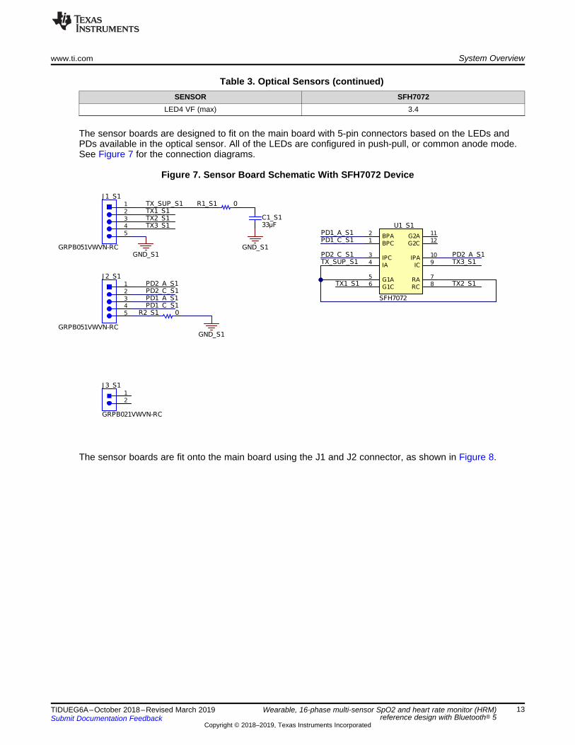
2.3.3 PPG MeasurementFor PPG measurement, three LEDs and two PDs are used in a single package. Table 3 lists details aboutthe SFH7072 from OSRAM®.
Table 3. Optical Sensors
SENSOR SFH7072Number of LEDs 4Number of PDs 2
LED1 color GreenLED1 wavelength 526 nm
LED2 color GreenLED2 wavelength 526 nm
LED3 color RedLED3 wavelength 660 nm
LED4 color IRLED3 wavelength 950 nm
LED1 VF (typ) 1.3LED1 VF (max) 1.8LED2 VF (typ) 2.1LED2 VF (max) 2.8LED3 VF (typ) 3LED3 VF (max) 3.4LED4 VF (typ) 3
www.ti.com System Overview
13TIDUEG6A–October 2018–Revised March 2019Submit Documentation Feedback
Copyright © 2018–2019, Texas Instruments Incorporated
Wearable, 16-phase multi-sensor SpO2 and heart rate monitor (HRM)reference design with Bluetooth® 5
Table 3. Optical Sensors (continued)SENSOR SFH7072
LED4 VF (max) 3.4
The sensor boards are designed to fit on the main board with 5-pin connectors based on the LEDs andPDs available in the optical sensor. All of the LEDs are configured in push-pull, or common anode mode.See Figure 7 for the connection diagrams.
Figure 7. Sensor Board Schematic With SFH7072 Device
The sensor boards are fit onto the main board using the J1 and J2 connector, as shown in Figure 8.

System Overview www.ti.com
14 TIDUEG6A–October 2018–Revised March 2019Submit Documentation Feedback
Copyright © 2018–2019, Texas Instruments Incorporated
Wearable, 16-phase multi-sensor SpO2 and heart rate monitor (HRM) referencedesign with Bluetooth® 5
Figure 8. PPG Connection From Sensor Board to AFE4420 Device on Main Board
The J1 connector has 5 connections: TX_SUP, TX drive pins, and GND. The J2 connector has 5connections: PD1 Anode and Cathode, PD2 Anode and Cathode, and GND. The connector inputs areprotected using ESD diodes (TPD1E10B06DPYR) from Texas Instruments. The TPD1E10B06 device is asingle-channel, ESD, TVS diode in a small 0402 package. This TVS protection product offers ±30-kVcontact ESD, ±30-kV IEC air-gap protection, and an ESD clamp circuit with a back-to-back TVS diode forbipolar or bidirectional signal support. The TX_SUP pin is decoupled using a 33-µF capacitor.
The PD signals are filtered using SMD Common Mode Chokes (having specifications as 90 Ω at 100 MHz,370-mA DCR 300 mΩ). The chokes help in improving the immunity to external common mode noisesignals and improve overall SNR of the system.
2.3.4 Selecting TX Supply (TX_SUP) Value for Driving LEDsTable 4 shows the recommended TX_SUP voltage range, taken from the AFE4420 device data sheet.
Table 4. Recommended TX_SUP Value
MINIMUM NOM MAXIMUM UNIT
RX_SUPReceiver supply: LDO Bypass mode 1.7 1.9 V
Receiver supply: LDO Enabled mode 1.9 Min (3.6,TX_SUP) V
IO_SUP I/O supply 1.7 RX_SUP VTX_SUP Transmitter supply 3 5.5 V
Digital inputs (Except CONTROL1, I2C_SPI_SEL) 0 IO_SUP V

� �
LHIN LIM
OUT maxOUT
IV I
2I
V
§ ·u � u K¨ ¸© ¹
OUT REFR35 R36
V VR36�
u
www.ti.com System Overview
15TIDUEG6A–October 2018–Revised March 2019Submit Documentation Feedback
Copyright © 2018–2019, Texas Instruments Incorporated
Wearable, 16-phase multi-sensor SpO2 and heart rate monitor (HRM)reference design with Bluetooth® 5
Table 4. Recommended TX_SUP Value (continued)MINIMUM NOM MAXIMUM UNIT
Analog inputs (And CONTROL1, I2C_SPI_SEL) 0 RX_SUP VTA Operating temperature range -40 85 °C
Table 5 shows the headroom voltage, VHR.
Table 5. Headroom Voltages
ILED_FSREGISTER TEX_REF VOLTAGE
1 LED DRIVER ON 2 LED DRIVERS ONTHROUGH SAME LED
2 LED DRIVERS ONTHROUGH 2 LEDS
MAXIMUMCURRENT VHR
MAXIMUMCURRENT VHR
MAXIMUMCURRENT VHR
00 150 mV 50 mA 320 mV 100 mA 370 mV 50 mA 345 mV01 300 mV 100 mA 600 mV 200 mA 650 mV 100 mA 625 mV11 375 mV 100 mA 700 mV 200 mA 750 mV 100 mA 725 mV
TX_SUP = VLED + VHR + 0.3 = 3.2 + 0.625 + 0.3 = 4.125 V (3)
Select TX_SUP = 4.2 V.
2.3.5 Generating TX Supply for Driving LEDs
Table 6. Specifications for TX_SUP
PARAMETER VALUEInput voltage 1.8 V to 3.0 V
Output voltage 4.2 VOutput current 50 mA
Output voltage ripple ±50 mV
2.3.5.1 Programming Output VoltageThe output voltage is programmed to 4.2 V using Equation 4, where VREF = 1.0 V. For best accuracy, thecurrent following through R36 should be 100 times larger than the FB pin leakage current.
(4)
Because VOUT = 4.2 V and R36 = 100 kΩ, R35 = 320 kΩ. TI recommends high-accuracy resistors forbetter output voltage accuracy. The TIDA-010029 device uses both resistors with 0.5% tolerance.
2.3.5.2 Maximum Output CurrentThe maximum output capability of the TPS61099 device is determined by the input-to-output ratio and thecurrent limit of the boost converter.
Equation 5 shows IOUT(max) = 300 mA ( VIN = 1.8 V, ILIM = 1 A, ILH = 350 mA, η = 85%, and VOUT = 4.2 V).
(5)

� � � �IN OUT IN
LH OUT
V V V 1.8 4.2 1.8 0.85f 1.48 MHz
L I V 2.2 0.35 4.2
u � u K u � u
u u P u u
System Overview www.ti.com
16 TIDUEG6A–October 2018–Revised March 2019Submit Documentation Feedback
Copyright © 2018–2019, Texas Instruments Incorporated
Wearable, 16-phase multi-sensor SpO2 and heart rate monitor (HRM)reference design with Bluetooth® 5
2.3.5.3 Input and Output Capacitor SelectionFor the best output and input voltage filtering, TI recommends low-ESR X5R or X7R ceramic capacitors.The input capacitor minimizes input voltage ripple, suppresses input voltage spikes, and provides a stablesystem rail for the device. An input capacitor value of 10 μF (C47) is used to improve transient behavior ofthe regulator and EMI behavior of the total power supply circuit. TI recommends placing a ceramiccapacitor as close as possible to the VIN and GND pins of the IC.
For the output capacitor of the VOUT pin, ceramic capacitors (C49 and C53) are placed as close aspossible to the VOUT and GND pins of the IC. This capacitor must be placed as close as possible to theVOUT and GND pins of the IC. From the power-stage point of view, the output capacitor sets the cornerfrequency of the converter, while the inductor creates a Right-Half-Plane-Zero. Consequently, with a largerinductor, a larger output capacitor must be used. The TPS61099x device is optimized to work with theinductor from 1 μH to 2.2 μH, so the minimal output capacitor value is 20 μF (nominal value). Increasingthe output capacitor makes the output ripple smaller in PWM mode.
2.3.5.4 Switching FrequencyThe switching frequency is calculated as Equation 6.
(6)
Figure 9 shows the schematic for the boost converter, TPS61099.
Figure 9. TPS61099 Boost Converter (VOUT = 4.2 V)
www.ti.com System Overview
17TIDUEG6A–October 2018–Revised March 2019Submit Documentation Feedback
Copyright © 2018–2019, Texas Instruments Incorporated
Wearable, 16-phase multi-sensor SpO2 and heart rate monitor (HRM)reference design with Bluetooth® 5
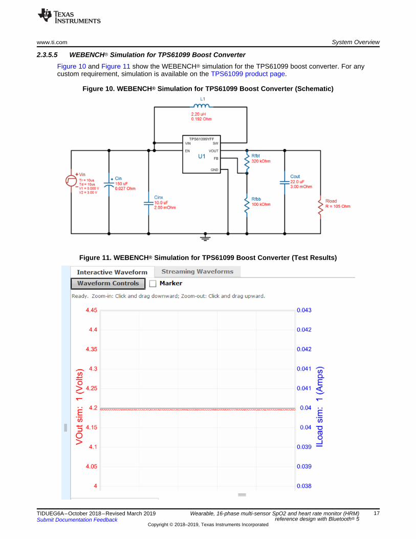
2.3.5.5 WEBENCH® Simulation for TPS61099 Boost ConverterFigure 10 and Figure 11 show the WEBENCH® simulation for the TPS61099 boost converter. For anycustom requirement, simulation is available on the TPS61099 product page.
Figure 10. WEBENCH® Simulation for TPS61099 Boost Converter (Schematic)
Figure 11. WEBENCH® Simulation for TPS61099 Boost Converter (Test Results)
� �
� �
OUT SW
OUT
OUT
I I 1 D
I 0.85 1 1 0.143
I 0.72845 A
Ku u �
u u �
SWOUT
I 0.85 1I 1.21A
D 0.7Ku u
OUT IN
OUT
V V 2.1 1.8D 0.143
V 2.1� �
OUT
IN
V 2.1D 0.7
V 3
OUT
FB
V 2.1R31 R32 1 51.1k 1 163 k
V 0.5
§ · § · u � u � :¨ ¸ ¨ ¸
© ¹© ¹
System Overview www.ti.com
18 TIDUEG6A–October 2018–Revised March 2019Submit Documentation Feedback
Copyright © 2018–2019, Texas Instruments Incorporated
Wearable, 16-phase multi-sensor SpO2 and heart rate monitor (HRM)reference design with Bluetooth® 5
2.3.6 Generating RX Supply for AFE4420
Table 7. Specifications for RX_SUP
PARAMETER VALUEInput voltage 1.8 V to 3.0 V
Output voltage 2.1 VOutput current 10 mA
Output voltage ripple ±50 mV
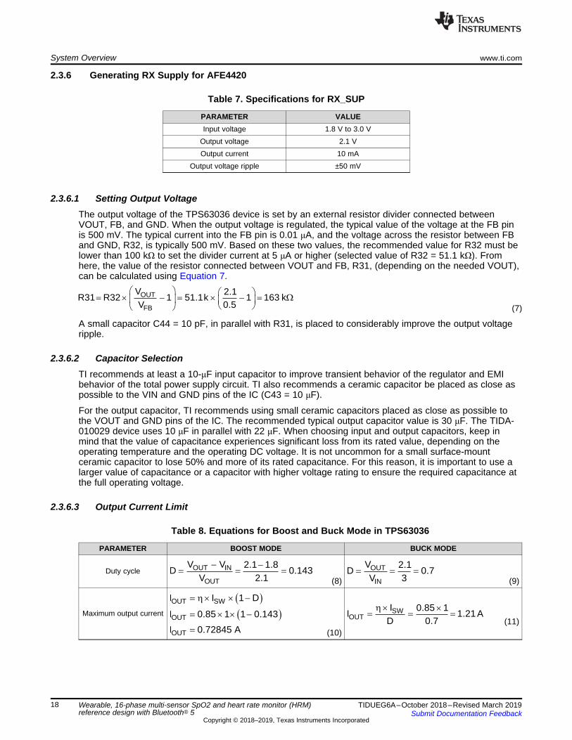
2.3.6.1 Setting Output VoltageThe output voltage of the TPS63036 device is set by an external resistor divider connected betweenVOUT, FB, and GND. When the output voltage is regulated, the typical value of the voltage at the FB pinis 500 mV. The typical current into the FB pin is 0.01 μA, and the voltage across the resistor between FBand GND, R32, is typically 500 mV. Based on these two values, the recommended value for R32 must belower than 100 kΩ to set the divider current at 5 μA or higher (selected value of R32 = 51.1 kΩ). Fromhere, the value of the resistor connected between VOUT and FB, R31, (depending on the needed VOUT),can be calculated using Equation 7.
(7)
A small capacitor C44 = 10 pF, in parallel with R31, is placed to considerably improve the output voltageripple.
2.3.6.2 Capacitor SelectionTI recommends at least a 10-μF input capacitor to improve transient behavior of the regulator and EMIbehavior of the total power supply circuit. TI also recommends a ceramic capacitor be placed as close aspossible to the VIN and GND pins of the IC (C43 = 10 μF).
For the output capacitor, TI recommends using small ceramic capacitors placed as close as possible tothe VOUT and GND pins of the IC. The recommended typical output capacitor value is 30 μF. The TIDA-010029 device uses 10 μF in parallel with 22 μF. When choosing input and output capacitors, keep inmind that the value of capacitance experiences significant loss from its rated value, depending on theoperating temperature and the operating DC voltage. It is not uncommon for a small surface-mountceramic capacitor to lose 50% and more of its rated capacitance. For this reason, it is important to use alarger value of capacitance or a capacitor with higher voltage rating to ensure the required capacitance atthe full operating voltage.
2.3.6.3 Output Current Limit
Table 8. Equations for Boost and Buck Mode in TPS63036
PARAMETER BOOST MODE BUCK MODE
Duty cycle(8) (9)
Maximum output current
(10)(11)
lNPEAK SW _MAX
V D 1.8 0.143I I 1 1.06435 A
2 f L 2 2 M 1u u
� � u u u u P
www.ti.com System Overview
19TIDUEG6A–October 2018–Revised March 2019Submit Documentation Feedback
Copyright © 2018–2019, Texas Instruments Incorporated
Wearable, 16-phase multi-sensor SpO2 and heart rate monitor (HRM)reference design with Bluetooth® 5
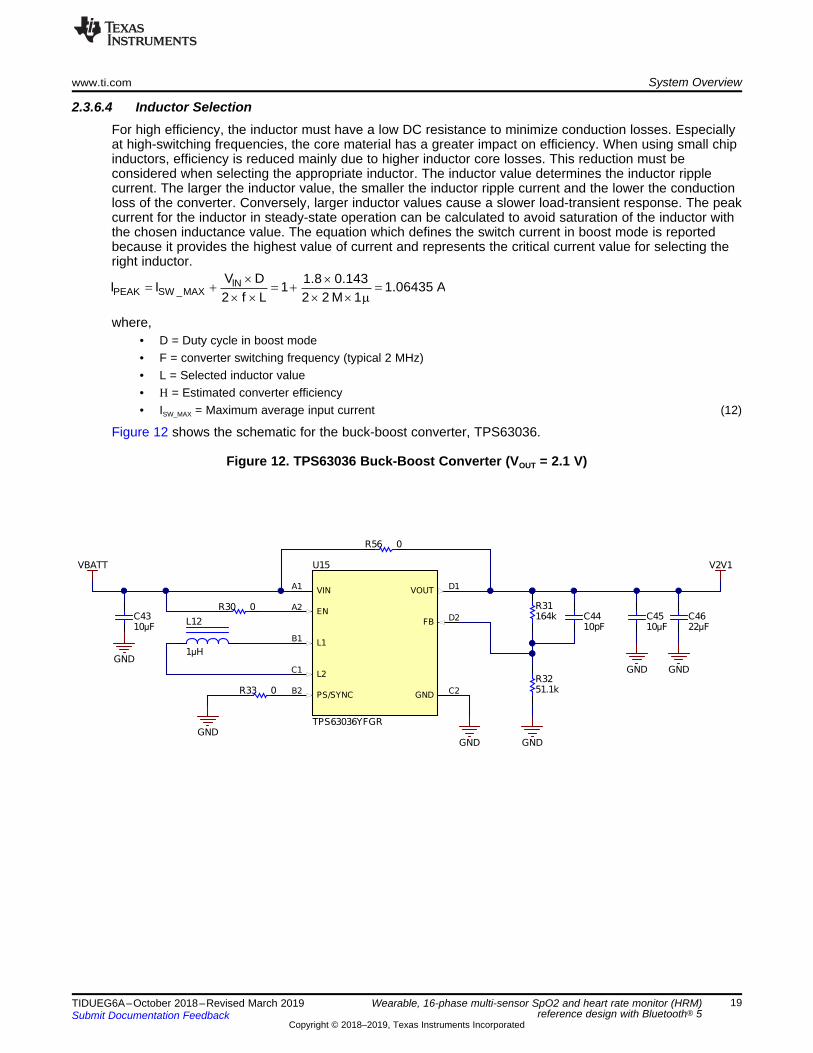
2.3.6.4 Inductor SelectionFor high efficiency, the inductor must have a low DC resistance to minimize conduction losses. Especiallyat high-switching frequencies, the core material has a greater impact on efficiency. When using small chipinductors, efficiency is reduced mainly due to higher inductor core losses. This reduction must beconsidered when selecting the appropriate inductor. The inductor value determines the inductor ripplecurrent. The larger the inductor value, the smaller the inductor ripple current and the lower the conductionloss of the converter. Conversely, larger inductor values cause a slower load-transient response. The peakcurrent for the inductor in steady-state operation can be calculated to avoid saturation of the inductor withthe chosen inductance value. The equation which defines the switch current in boost mode is reportedbecause it provides the highest value of current and represents the critical current value for selecting theright inductor.
where,• D = Duty cycle in boost mode• F = converter switching frequency (typical 2 MHz)• L = Selected inductor value• Η = Estimated converter efficiency• ISW_MAX = Maximum average input current (12)
Figure 12 shows the schematic for the buck-boost converter, TPS63036.
Figure 12. TPS63036 Buck-Boost Converter (VOUT = 2.1 V)

System Overview www.ti.com
20 TIDUEG6A–October 2018–Revised March 2019Submit Documentation Feedback
Copyright © 2018–2019, Texas Instruments Incorporated
Wearable, 16-phase multi-sensor SpO2 and heart rate monitor (HRM)reference design with Bluetooth® 5
2.3.6.5 TINA-TI ™ Simulation for TPS63036Figure 13 and Figure 14 show the TINA-TI™ simulation for the TPS63036 buck-boost converter. TheTINA simulation file for any custom requirement can be downloaded from the TPS63036 product page.
Figure 13. TINA-TI™ Simulation for TPS61099 Boost Converter (Schematic)
Figure 14. TINA-TI™ Simulation for TPS61099 Boost Converter (Test Results)

www.ti.com System Overview
21TIDUEG6A–October 2018–Revised March 2019Submit Documentation Feedback
Copyright © 2018–2019, Texas Instruments Incorporated
Wearable, 16-phase multi-sensor SpO2 and heart rate monitor (HRM)reference design with Bluetooth® 5
2.3.7 Generating I/O SupplyThe I/O supply selected is the same as RX-SUP (2.1 V) through R28 (0 Ω). Another option is to mount anLDO at position U18.
Figure 15. IO_SUP Same as RX_SUP
NOTE: U18 is currently not mounted on the TIDA-010029 board. U18 can be mounted if IO_SUPmust be different than 2.1 V. LDOs with low drop-out voltages (for example, < 300 mV) havehigher quiescent currents which may affect the battery operating time.
2.3.8 Battery Input and Reservoir CapacitorsThe power source for this TIDA-010029 device is the CR3032, a lithium-ion coin cell. Selection of theCR2032 coin-cell battery as the power source is due to the ubiquity of the battery type, particularly insmall form factor systems. The voltage characteristics of the CR3032 lithium-ion coin cell battery are alsoideal. The output voltage remains relatively flat throughout the discharge life until the cell is nearlydepleted. When the remaining charge in the coin-cell battery is nearly depleted, the output voltage dropsoff relatively quickly. The temperature characteristics of lithium-ion batteries are also superior to that ofalkaline cells, particularly at lower temperatures. This superiority is due to lithium-ion cells having a non-aqueous electrolyte that performs better than the aqueous electrolytes commonly found in alkalinebatteries.
Figure 16. Battery Connector and Reservoir

System Overview www.ti.com
22 TIDUEG6A–October 2018–Revised March 2019Submit Documentation Feedback
Copyright © 2018–2019, Texas Instruments Incorporated
Wearable, 16-phase multi-sensor SpO2 and heart rate monitor (HRM)reference design with Bluetooth® 5
Given an appropriate weather-proof enclosure, this TI reference design system is suited for both indoorand outdoor use. Immediately following the battery is a bulk capacitor. This TI reference design uses acoin-cell battery tray that prevents an end-user from inserting the battery backwards, which may eliminatethe need for the reverse Schottky diode. The bulk capacitor is sized to prevent too much voltage sag,particularly during the initial transition into the on state, as shown in Figure 16.
2.3.9 Battery Life CalculationsThis section explains the calculations for battery life of the CR3032 coin-cell battery. The possible currentpaths in this design are:• Battery to AFE4420, through the Boost (TPS61099) to the TX_SUP pin• Battery to AFE4420, through the Buck-Boost (TPS63036) to the RX_SUP/IO_SUP pin• Battery to CC2640R2F, through the Buck-Boost (TPS63036) to the VDDS2/3 pin• Battery to CC2640R2F, directly to the VDDS pin
2.3.9.1 AFE4420 Current ConsumptionThe current consumption of the AFE4420 device depends on the sampling rate (for example, PTT modeat 1-kHz sampling rate for both ECG and PPG).
Typical specifications are at TA = 25°C; TX_SUP = 5 V, RX_SUP = 1.8 V (with CONTROL1 = 1.8 V tobypass internal LDOs), IO_SUP = 1.8 V, external clock mode with 32-kHz clock on CLK pin (period = tTE =31.25 µs), the AFE operates with ULP mode enabled (ENABLE_ULP = 1); PPG: 1-kHz sampling rate,SAMP width of 3 × tTE, LED ON width of 4 × tTE, CF chosen such that there are 7-8 TIA time constantswithin the SAMP width, NUMAV = 1 (2 ADC averages), noise-reduction filter bandwidth set to 2.5 kHz, CIN= 100 pF (capacitor across the input pins to model the zero bias differential capacitance of the PD); ECG:1-kHz sampling rate, INA gain of 12, chopper mode enabled (unless otherwise noted).
(1) Normal operation refers to operation at 25 Hz PRF in external clock mode with a 128 kHz clock, with the device in an activestate for 3.5% of the PRF cycle, In Light sleep state for 1% of the PRF cycle and in deep sleep state for 95.5% of the PRF cycle.
(2) External clock switched off.(3) In LDO Bypass mode: with PDN_BG_IN_DEEP_SLEEP bit set to 1 along with the PDNAFE bit set to 1. When operation in the
LDO Enable mode, the software power-down current on RX_SUP is about 8 µA.(4) This current depends on the percentage of time for which the I2C_CLK is low; and scales with PRF and the number of FIFO
samples generated in each cycle. This extra component of current is negligible when operating in the SPI interface mode.(5) LED currents are set to 0 mA.
Table 9. Current Consumption for AFE4420 in Different Modes
PARAMETER TEST CONDITIONS MIN TYP MAX UNITCURRENT CONSUMPTION
RX_SUP current excluding switching currentfrom I2C or SPI readout
Normal operation (1) 21
µAHardware power-down (PWDN)mode (2) <1
Software power-down (PDNAFE)mode (2) (3) 1
RX_SUP current resulting from switchingcurrent at I2C readout
While reading out 100 samples of theFIFO every second. (4) 3
µAPower-down mode 0
IO_SUP current
Normal operation (1) 1
µAHardware power-down (PWDN)mode (2) <1
Software power-down (PDNAFE)mode (2) (3) 1
TX_SUP current
Normal operation (1) (5) 1.5
µAHardware power-down (PWDN)mode (2) (5) <1
Software power-down (PDNAFE)mode (2) (5) 1

PRF (Hz)
RX
_SU
P C
urre
nt fo
r F
IFO
Rea
dout
(P
A)
5 15 25 35 45 55 65 75 85 951000
1
2
3
4
5
6
7
8
D016
I2C ModeSPI Mode
PRF (Hz)
Ave
rage
Rec
eive
r C
urre
nt (P
A)
10 20 30 40 50 60 70 80 90 1000
10
20
30
40
50
60
70
80
90
100
110
120
D015
LDO Enable Mode INT OSCLDO Enable Mode EXT CLKLDO Bypass Mode INT OSCLDO Bypass Mode EXT CLK
www.ti.com System Overview
23TIDUEG6A–October 2018–Revised March 2019Submit Documentation Feedback
Copyright © 2018–2019, Texas Instruments Incorporated
Wearable, 16-phase multi-sensor SpO2 and heart rate monitor (HRM)reference design with Bluetooth® 5
Figure 17. RX_SUP Current vs PRF (Excluding FIFO ReadoutCurrent) Figure 18. RX_SUP Current for FIFO Readout
The TX_SUP current is taken to be 3 mA at normal operating conditions (10% duty cycle for 100 mA) inthe worst case.
Over-operating free-air temperature range unless otherwise noted.
Table 10. LED Drive Currents With Duty Cycles
PARAMETER MIN MAX UNIT
Supply voltage range
RX_SUP to GND; LDObypassed –0.3 2.1
VRX_SUP to GND; LDOenabled –0.3 4
IO_SUP to GND –0.3 Min [4,(RX_SUP+0.3)]TX_SUP to GND –0.3 6
Voltage applied to analog inputs and topins CONTROL1, I2C_SPI_SEL
Max [–0.3, (GND –0.3)]
Min [4.0, (RX_SUP +0.3)] V
Voltage applied to digital inputs Max [–0.3, (GND –0.3)]
Min [4.0, (IO_SUP +0.3)] V
Duty cycle (cumulative): sum of all LEDphase durations as a function of the totalperiod
50-mA LED current 10%100-mA LED current 5%200-mA LED current 2.8%
Tstg Storage temperature –60 150 °C
The RX_SUP and IO_SUP current are taken to be 700 µA (600 µA + 10 µA (I/O) + 50 µA (LDO enabled)+ 40 µA (buffer)).

System Overview www.ti.com
24 TIDUEG6A–October 2018–Revised March 2019Submit Documentation Feedback
Copyright © 2018–2019, Texas Instruments Incorporated
Wearable, 16-phase multi-sensor SpO2 and heart rate monitor (HRM)reference design with Bluetooth® 5
2.3.9.2 CC2640R2F Current ConsumptionThe net total of the current supplied to the CC2640R2F device is taken as 10 mA, including peripheralsand TX only. A 50-µA average current is chosen at VDDS2/3.
Measured on the TI CC2650EM-5XD reference design with Tc = 25°C, VDDS = 3.0 V with an internalDC/DC converter, unless otherwise noted.
(1) Single-ended RF mode is optimized for size and power consumption. Measured on CC2650EM-4XS.(2) Differential RF mode is optimized for RF performance. Measured on CC2650EM-5XD.(3) Iperi is not supported in Standby or Shutdown.
Table 11. Power Consumption for CC2640R2F
PARAMETER TEST CONDITIONS MIN TYP MAX UNIT
Icore Core current consumption
Reset. RESET_N pin asserted or VDDS belowPower-on-Reset threshold 100
nAShutdown. No clocks running, no retention 150Standby. With RTC, CPU, RAM and (partial)register retention. RCOSC_LF 1.1
µA
Standby. With RTC, CPU, RAM and (partial)register retention. XOSC_LF 1.3
Standby. With Cache, RTC, CPU, RAM and(partial) register retention. RCOSC_LF 2.8
Standby. With Cache, RTC, CPU, RAM and(partial) register retention. XOSC_LF 3.0
Idle. Supply Systems and RAM powered. 550
Active. Core running CoreMark 1.45 mA +31 µA/MHz
Radio RX (1) 5.9
mARadio RX (2) 6.1Radio TX, 0-dBm output power (1) 6.1Radio TX, 5-dBm output power (2) 9.1
Peripheral Current Consumption (Adds to core current Icore for each peripheral unit activated) (3)
Iperi
Peripheral power domain Delta current with domain enabled 20 µASerial power domain Delta current with domain enabled 13 µA
RF Core Delta current with power domain enabled,clock enabled, RF core idle 237 µA
µDMA Delta current with clock enabled, module idle 130 µATimers Delta current with clock enabled, module idle 113 µAI2C Delta current with clock enabled, module idle 12 µAI2S Delta current with clock enabled, module idle 36 µASSI Delta current with clock enabled, module idle 93 µAUART Delta current with clock enabled, module idle 164 µA

� �net idleI 5.62 A 22 A 600 A 627.62 A P � P � P P
� �net standbyI 5.62 A 22 A 5 A 32.62 A P � P � P P
� �net shutdownI 5.62 A 22 A 0.2 A 27.82 A P � P � P P
O OTPS63036
imin
V I 2.1 2 AI 22 A
V 1.8 0.5
u u P P
u K u
O OTPS61099
imin
V I 4.2 2 AI 5.62 A
V 1.8 0.85
u u P P
u K u
� �mAh
Life hrs 500 0.85 16.255 hrs26.145 mA
u
netI 13.725 mA 0.42 mA 12 mA 26.145 mA � �
O OTPS63036
imin
V I 2.1 180 AI 420 A
V 1.8 0.5
u u P P
u K u
O OTPS61099
imim
V I 4.2 5 mAI 13.725 mA
V 1.8 0.85
u u
u K u
www.ti.com System Overview
25TIDUEG6A–October 2018–Revised March 2019Submit Documentation Feedback
Copyright © 2018–2019, Texas Instruments Incorporated
Wearable, 16-phase multi-sensor SpO2 and heart rate monitor (HRM)reference design with Bluetooth® 5
2.3.9.3 On-State Current CalculationsThe reflected current on the input side of the TPS61099 device is given in Equation 13.
(13)
Where efficiency is taken to be 85% (maximum 88% at low load of 10 µA), see Equation 14.
(14)
Where efficiency is taken to be 50%. Therefore, the net total current from all the branch is given inEquation 15.
(15)
Therefore, the calculated battery life of the coin cell is given in Equation 16.
For CR3032, rating = 500 mAh
(16)
The measured currents on the TIDA-010029 device are much less than these calculated values becausethe calculations are for worst-case performance. The measured values are as follows.
Inet = 4.09 mA at Vin = 3 V
Inet = 6.05 mA at Vin = 1.8 V
So Iavg = 5.06 mA, which gives battery life of 98.7 hours.
2.3.9.4 Off-State Current Calculations (Considering Battery Voltage = 3 V)The RX_SUP current at low-power operation (15 µA at software power-down mode and 1 µA at hardwarepower-down mode) = 16 µA (worst case). The TX_SUP current at low-power operation (1 µA at softwarepower-down mode, 1 µA at hardware power-down mode) = 2 µA (worst case). The net total currentsupplied to the CC2640R2F device is taken as 200 nA (shutdown), 5 µA (standby), and 550 µA (idle).
Reflected current on the input side of TPS61099 is:
(17)
(18)
(19)
(20)
(21)
Table 12 lists the battery lifetime for the cases shown.
Table 12. Battery Life Calculations
MODE ON-STATECURRENT (mA)
OFF-STATECURRENT (µA)
BATTERY LIFEFOR
1 s/MIN DUTYCYCLE (DAYS)
BATTERY LIFEFOR
5 s/MIN DUTYCYCLE (DAYS)
BATTERY LIFEFOR
20 s/MIN DUTYCYCLE (DAYS)
Shutdown 4.09 27 220 57 15Standby 4.09 32 209 56 15
Idle 4.09 627 30 22.7 11.7

System Overview www.ti.com
26 TIDUEG6A–October 2018–Revised March 2019Submit Documentation Feedback
Copyright © 2018–2019, Texas Instruments Incorporated
Wearable, 16-phase multi-sensor SpO2 and heart rate monitor (HRM)reference design with Bluetooth® 5
2.3.10 External Memory
NOTE: U16 is currently not mounted on the TIDA-010029 board. It can be mounted if an external-data log memory is required. When selecting the memory,check the IO_SUP value andoperating VCC for the memory.
The TIDA-010029 board has a provision for external memory connection over SPI, as shown in Figure 19.
Figure 19. External Memory
Table 13 lists the connections between the memory chip and the CC2640R2F device.
Table 13. Connections Between Memory and CC2640R2F
MEMORY PINNUMBER FUNCTION CC2640R2F PIN
NUMBER FUNCTION COMMENTS
1 /CS 18 DIO_12 Memory SPI enable2 D0 (IO1) 15 DIO_9 SPI OUT for memory3 /WP (IO2) 19 DIO_13 Memory write protect5 D1 (IO0) 14 DIO_8 SPI IN for memory6 CLK 16 DIO_10 SPI CLK for memory7 /HOLD or /RESET 20 DIO_14 Memory hold

www.ti.com System Overview
27TIDUEG6A–October 2018–Revised March 2019Submit Documentation Feedback
Copyright © 2018–2019, Texas Instruments Incorporated
Wearable, 16-phase multi-sensor SpO2 and heart rate monitor (HRM)reference design with Bluetooth® 5
2.3.11 LED IndicationsThe board has three LEDs for indication, see Figure 20 and Figure 16.
Figure 20. LED Indications
Table 14 lists the functions of each LED.
Table 14. LED Indications
LED NUMBER COLOR FUNCTIOND1 Green Incoming power supply or battery indicatorD3 Red Low-battery indicationD4 Red BLE connection status

PCB Antenna
CC2640R2F
Connectors for Optical Sensor
Battery Input Circuit
TPS63036
Memory
CM Chokes for PD signals
AFE4420
TPS61099
Programming Connector
LED Indications
Hardware, Software, Testing Requirements, and Test Results www.ti.com
28 TIDUEG6A–October 2018–Revised March 2019Submit Documentation Feedback
Copyright © 2018–2019, Texas Instruments Incorporated
Wearable, 16-phase multi-sensor SpO2 and heart rate monitor (HRM)reference design with Bluetooth® 5
3 Hardware, Software, Testing Requirements, and Test Results
3.1 Required Hardware and Software
3.1.1 HardwareFigure 21 and Figure 22 show top and bottom views of the TIDA-010029 PCB, respectively. The importantsections are highlighted with yellow boxes and captions.
Figure 21. TIDA-010029 PCB - Top ViewBattery Holder (BT1) Not Mounted
Figure 22. TIDA-010029 PCB - Bottom View

www.ti.com Hardware, Software, Testing Requirements, and Test Results
29TIDUEG6A–October 2018–Revised March 2019Submit Documentation Feedback
Copyright © 2018–2019, Texas Instruments Incorporated
Wearable, 16-phase multi-sensor SpO2 and heart rate monitor (HRM)reference design with Bluetooth® 5
3.1.1.1 Connecting Optical Sensor Boards to Main BoardFigure 23 shows the PPG board mounted on the main board.
Figure 23. PPG Sensor Board Mounted on Main Board (Top View)

Hardware, Software, Testing Requirements, and Test Results www.ti.com
30 TIDUEG6A–October 2018–Revised March 2019Submit Documentation Feedback
Copyright © 2018–2019, Texas Instruments Incorporated
Wearable, 16-phase multi-sensor SpO2 and heart rate monitor (HRM)reference design with Bluetooth® 5
Figure 24 shows PPG sensor boards.
Figure 24. PPG Sensor Boards
Figure 25. PPG Sensor Board Mounted on Main Board (Side View)

www.ti.com Hardware, Software, Testing Requirements, and Test Results
31TIDUEG6A–October 2018–Revised March 2019Submit Documentation Feedback
Copyright © 2018–2019, Texas Instruments Incorporated
Wearable, 16-phase multi-sensor SpO2 and heart rate monitor (HRM)reference design with Bluetooth® 5
3.1.1.2 Configuration of PPG Sensor BoardsThe PPG sensor board uses the SFH 7072 device from OSRAM. The default configuration for the PPGsensor board is as follows:• LED1 (green1) of the SFH7072 = connected to TX4 of the AFE4420 device• LED2 (green2) of the SFH7072 = not connected to the AFE4420 device• LED3 (red) of the SFH7072 = connected to TX2 of the AFE4420 device• LED4 (IR) of the SFH7072 = connected to TX3 of the AFE4420 device• The Dual_PD_Enable bit is set in the 0x4E register in the AFE4420 device (see Figure 26).• PD1 of the AFE4420 device is connected to Broadband PD, and PD2 of the AFE4420 device is
connected to Infrared-Cut PD.
Figure 26. Timing and Settings for SFH 7072 PPG Sensor
NOTE: Figure 26 is a screen shot from the AFE4420EVM GUI (available at AFE4420EVM).

TIDA-010029 Board
LAUNCHXL_CC2640R2
Micro-USB cable to connect LAUNCHXL-CC2640R2 with PC
CCS 7.0 (or higher version) installed on
PC
Hardware, Software, Testing Requirements, and Test Results www.ti.com
32 TIDUEG6A–October 2018–Revised March 2019Submit Documentation Feedback
Copyright © 2018–2019, Texas Instruments Incorporated
Wearable, 16-phase multi-sensor SpO2 and heart rate monitor (HRM)reference design with Bluetooth® 5
3.1.2 SoftwareThe following software tools were used to test and obtain the results for this TI reference design:• Code Composer Studio™ (CCS), version 7 or higher (This software should be installed with CC26xx
support. Run installer again if CC26xx support is not already installed.)• SIMPLELINK-CC2640R2-SDK Software• LAUNCHXL-CC2640R2• LabVIEW™ 2016 Development Engine or Runtime Engine (32-bit)• JAVA Runtime Engine (32-bit)
The following instructions are for PCs that CCS, SIMPLELINK-CC2640R2-SDK, LabVIEW and JAVA arealready installed. Download the LabVIEW application setup (zip file) from the TIDA-010029 product page.This setup installs the firmware containing four project folders (two for the transmit section and two for thereceive section) and the LabView application folder containing executable file and source files.
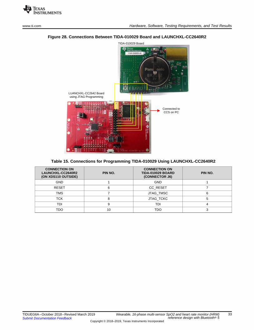
3.1.2.1 Software Loading for TIDA-010029 Board (Transmit Side of BLE)1. Plug in the LAUNCHXL-CC2640R2 board on the USB port of the PC. See the setup in Figure 27 and
Figure 28. Table 15 lists the connections between the TIDA-010029 board and the LAUNCHXL-CC2640R2 board.
Figure 27. Programming TIDA-010029 Board Using LAUNCHXL-CC2640R2
2. Insert one CR3032 battery into the BT1 connector on the TIDA-010029 board, and power it on byusing the S2 switch, and ensure J8 is shorted on the TIDA-010029 board.
3. Open CCS as administrator by right-clicking on the CCS icon and run as administrator.4. Click on the Project option in the main toolbar and then click Import CCS projects.5. Browse to select the installed firmware (Default: C:\Program Files (x86)\Texas Instruments\TIDA-
010029\TIDA-010029_firmware) and import all projects. Click the OK button.6. Click View, Project Explorer and select TIDA-010029_firmware_tx.7. Click on the Run and Debug buttons. This action programs the board with the selected project file.8. Disconnect the TIDA-010029 board from the LAUNCHXL-CC2640R2 device.
Connected to CCS on PC
LUANCHXL-CC2642 Board using JTAG Programming
TIDA-010029 Board
www.ti.com Hardware, Software, Testing Requirements, and Test Results
33TIDUEG6A–October 2018–Revised March 2019Submit Documentation Feedback
Copyright © 2018–2019, Texas Instruments Incorporated
Wearable, 16-phase multi-sensor SpO2 and heart rate monitor (HRM)reference design with Bluetooth® 5
Figure 28. Connections Between TIDA-010029 Board and LAUNCHXL-CC2640R2
Table 15. Connections for Programming TIDA-010029 Using LAUNCHXL-CC2640R2
CONNECTION ONLAUNCHXL-CC2640R2(ON XDS110 OUTSIDE)
PIN NO.CONNECTION ON
TIDA-010029 BOARD(CONNECTOR J6)
PIN NO.
GND 1 GND 1RESET 6 CC_RESET 7
TMS 7 JTAG_TMSC 6TCK 8 JTAG_TCKC 5TDI 9 TDI 4TDO 10 TDO 3

Hardware, Software, Testing Requirements, and Test Results www.ti.com
34 TIDUEG6A–October 2018–Revised March 2019Submit Documentation Feedback
Copyright © 2018–2019, Texas Instruments Incorporated
Wearable, 16-phase multi-sensor SpO2 and heart rate monitor (HRM)reference design with Bluetooth® 5
3.1.2.2 LabVIEW™ File Execution for Checking Measurement Data (Receive Side of BLE)
NOTE: Only one device, the LAUNCHXL-CC2640R2 or XDS110, can be connected to the PC whilerunning the executable file.
1. Insert one CR3032 battery into the BT1 connector on the TIDA-010029 board and power it on by usingthe S2 switch. Ensure J8 is shorted on the TIDA-010029 board. Ignore this step if it was already doneduring programming of the TIDA-010029 board.
2. Revert back to the original LaunchPAD jumper settings.3. Plug in the LAUNCHXL-CC2640R2 device on the USB port of the PC.4. Open the Setup_TIDA-010029.exe file and go through the installation process, explained as follows.
1. Click Next on the Setup Welcome screen shown in Figure 29.
Figure 29. Setup Welcome Screen

www.ti.com Hardware, Software, Testing Requirements, and Test Results
35TIDUEG6A–October 2018–Revised March 2019Submit Documentation Feedback
Copyright © 2018–2019, Texas Instruments Incorporated
Wearable, 16-phase multi-sensor SpO2 and heart rate monitor (HRM)reference design with Bluetooth® 5
2. Accept the agreement and click Next on the License Agreement screen shown in Figure 30.
Figure 30. License Agreement Screen
3. Click Next on the Installation Directory screen shown in Figure 31.
Figure 31. Installation Directory Screen

Hardware, Software, Testing Requirements, and Test Results www.ti.com
36 TIDUEG6A–October 2018–Revised March 2019Submit Documentation Feedback
Copyright © 2018–2019, Texas Instruments Incorporated
Wearable, 16-phase multi-sensor SpO2 and heart rate monitor (HRM)reference design with Bluetooth® 5
4. Click Next on the Select Components screen shown in Figure 32.
Figure 32. Select Components Screen
5. Click Next on the Ready to Install screen as shown in Figure 33.
Figure 33. Ready to Install Screen

www.ti.com Hardware, Software, Testing Requirements, and Test Results
37TIDUEG6A–October 2018–Revised March 2019Submit Documentation Feedback
Copyright © 2018–2019, Texas Instruments Incorporated
Wearable, 16-phase multi-sensor SpO2 and heart rate monitor (HRM)reference design with Bluetooth® 5
The setup starts installing and the progress screen is displayed as shown in Figure 34.
Figure 34. Installing GUI
6. When installed, click Finish. Look for the TIDA-010029 Application.exe at the installed location(default location: C:\Program Files (x86)\Texas Instruments\TIDA-010029\TIDA-010029Application).

Hardware, Software, Testing Requirements, and Test Results www.ti.com
38 TIDUEG6A–October 2018–Revised March 2019Submit Documentation Feedback
Copyright © 2018–2019, Texas Instruments Incorporated
Wearable, 16-phase multi-sensor SpO2 and heart rate monitor (HRM)reference design with Bluetooth® 5
Figure 35. Completing TIDA-010029 Setup Wizard

www.ti.com Hardware, Software, Testing Requirements, and Test Results
39TIDUEG6A–October 2018–Revised March 2019Submit Documentation Feedback
Copyright © 2018–2019, Texas Instruments Incorporated
Wearable, 16-phase multi-sensor SpO2 and heart rate monitor (HRM)reference design with Bluetooth® 5
While launching the GUI, a splash screen appears, as shown in Figure 36.
Figure 36. Splash Screen on Launching TIDA-010029 GUI
The Instructions tab provides instructions and safety precautions as shown in Figure 37.
Figure 37. TIDA-010029 GUI Instructions Tab

Hardware, Software, Testing Requirements, and Test Results www.ti.com
40 TIDUEG6A–October 2018–Revised March 2019Submit Documentation Feedback
Copyright © 2018–2019, Texas Instruments Incorporated
Wearable, 16-phase multi-sensor SpO2 and heart rate monitor (HRM)reference design with Bluetooth® 5
The Configurations tab shown in Figure 38 provides information about the software paths.1. Ensure that the CCS base-folder path is set to <CCS installation path>\ccsv7\ccs_base.2. Ensure that the project .OUT file path is set to <installation folder>\TIDA-010029_firmware\TIDA-
010029_firmware_rx\FlashROM_StackLibrary\TIDA-010029_firmware_rx.out.3. The START/STOP button can connect and program the LAUNCHXL-CC2640R2 device to capture the
data. After clicking the START/STOP button, the TIDA-010029 board must immediately be powercycled using the S2 switch. The START/STOP button can also disconnect the link.
4. The Pulse Repetition Frequency (PRF) can be changed.
Figure 38. TIDA-010029 GUI Configurations Tab
www.ti.com Hardware, Software, Testing Requirements, and Test Results
41TIDUEG6A–October 2018–Revised March 2019Submit Documentation Feedback
Copyright © 2018–2019, Texas Instruments Incorporated
Wearable, 16-phase multi-sensor SpO2 and heart rate monitor (HRM)reference design with Bluetooth® 5
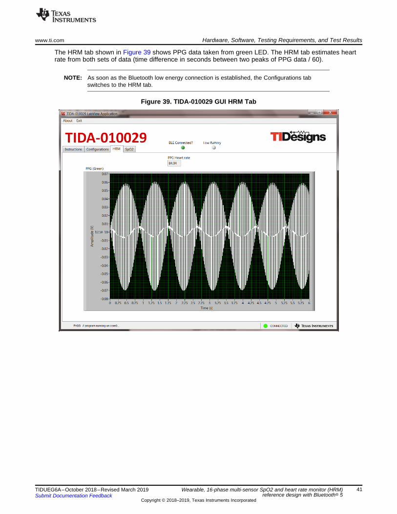
The HRM tab shown in Figure 39 shows PPG data taken from green LED. The HRM tab estimates heartrate from both sets of data (time difference in seconds between two peaks of PPG data / 60).
NOTE: As soon as the Bluetooth low energy connection is established, the Configurations tabswitches to the HRM tab.
Figure 39. TIDA-010029 GUI HRM Tab
Hardware, Software, Testing Requirements, and Test Results www.ti.com
42 TIDUEG6A–October 2018–Revised March 2019Submit Documentation Feedback
Copyright © 2018–2019, Texas Instruments Incorporated
Wearable, 16-phase multi-sensor SpO2 and heart rate monitor (HRM)reference design with Bluetooth® 5
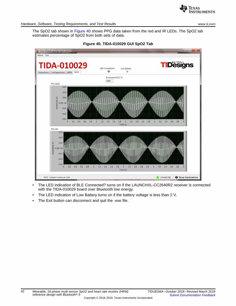
The SpO2 tab shown in Figure 40 shows PPG data taken from the red and IR LEDs. The SpO2 tabestimates percentage of SpO2 from both sets of data.
Figure 40. TIDA-010029 GUI SpO2 Tab
• The LED indication of BLE Connected? turns on if the LAUNCHXL-CC2640R2 receiver is connectedwith the TIDA-010029 board over Bluetooth low energy.
• The LED indication of Low Battery turns on if the battery voltage is less than 2 V.• The Exit button can disconnect and quit the .exe file.

www.ti.com Hardware, Software, Testing Requirements, and Test Results
43TIDUEG6A–October 2018–Revised March 2019Submit Documentation Feedback
Copyright © 2018–2019, Texas Instruments Incorporated
Wearable, 16-phase multi-sensor SpO2 and heart rate monitor (HRM)reference design with Bluetooth® 5
3.2 Testing and ResultsThis section describes the test setup and test results for the TIDA-010029 board. Figure 41 shows the testsetup for capturing data.
Figure 41. Test Setup for Capturing Data
3.2.1 Test Setup1. Plug in the LAUNCHXL-CC2640R2 device on the USB port of the PC.2. Open the TIDA-010029 Application.exe file.3. Connect the human body (fingers or wrist) to the TIDA-010029 board for the measurement. Ensure
that the PPG sensor on the bottom side of the board is covered by a finger.4. Ensure that the paths are correct for the CCS Base Folder and Project .out file on the Configurations
tab.5. Click on the START/STOP button in the Configurations tab on the TIDA-010029 GUI.6. Power-cycle the TIDA-010029 board by toggling the S2 switch.7. The Configurations Tab shows the following message:
Welcome...Advanced filtering is disabled in the Run Time EnginePASS // core0 connected as Cortex_M3_0...PASS // program file loaded on core0...PASS // program running on core0...
Hardware, Software, Testing Requirements, and Test Results www.ti.com
44 TIDUEG6A–October 2018–Revised March 2019Submit Documentation Feedback
Copyright © 2018–2019, Texas Instruments Incorporated
Wearable, 16-phase multi-sensor SpO2 and heart rate monitor (HRM)reference design with Bluetooth® 5
As soon as the TIDA-010029 board connects to the receiving LAUNCHXL-CC2640R2 board, the BLEConnected? LED turns on, and the HRM tab should be open showing PPG (green LED). The SpO2tab can be used for measuring PPG data from the red and IR LEDs.
8. Once evaluation is over, click on the START/STOP button in the Configurations tab. The tab shows thefollowing message:PASS // closing tcp session on port 1444..
9. Click on the Exit button to quit the .exe file.
3.2.2 Test Results
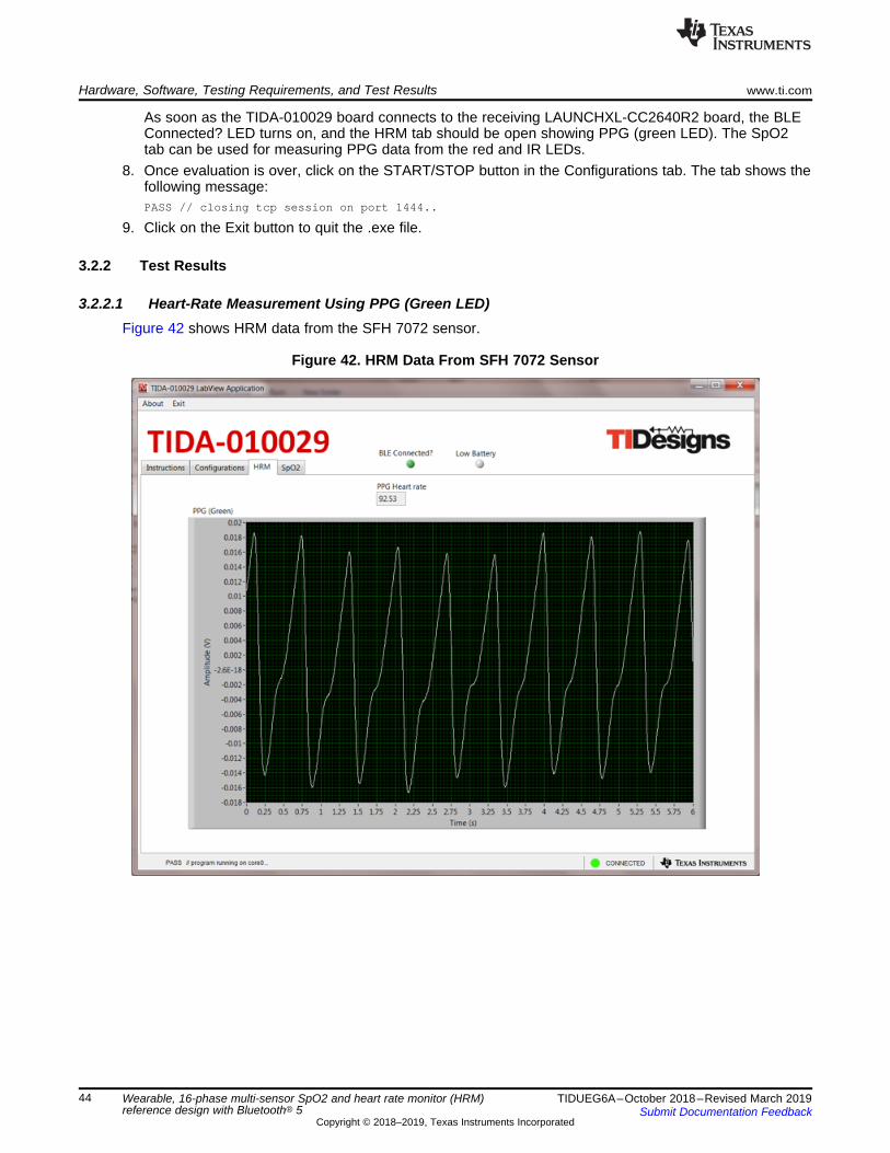
3.2.2.1 Heart-Rate Measurement Using PPG (Green LED)Figure 42 shows HRM data from the SFH 7072 sensor.
Figure 42. HRM Data From SFH 7072 Sensor

www.ti.com Hardware, Software, Testing Requirements, and Test Results
45TIDUEG6A–October 2018–Revised March 2019Submit Documentation Feedback
Copyright © 2018–2019, Texas Instruments Incorporated
Wearable, 16-phase multi-sensor SpO2 and heart rate monitor (HRM)reference design with Bluetooth® 5
3.2.2.2 SpO2 Measurement Using Red and IR LEDsFigure 43 shows SpO2 data from the SFH 7072 sensor.
Figure 43. SpO2 Data From SFH 7072 Sensor

Hardware, Software, Testing Requirements, and Test Results www.ti.com
46 TIDUEG6A–October 2018–Revised March 2019Submit Documentation Feedback
Copyright © 2018–2019, Texas Instruments Incorporated
Wearable, 16-phase multi-sensor SpO2 and heart rate monitor (HRM)reference design with Bluetooth® 5
3.2.2.3
NOTE: During testing, it was observed that the power line noise and other motion artifacts gettingcoupled to the PPG signals drastically reduced the SNR. For HRM applications, it isimperative to remove the noise and baseline drift. Heart-rate estimation usually requires analgorithm that filters the noise and detects the beat-to-beat heart rate and average heart rate.Even under rest conditions, extraction of heart rate data can get complicated, due to suddenchanges in the DC level of the signal, due to respiration and motion artifacts. The heart ratecan be calculated by measuring the separation between the successive peaks of the signalafter eliminating the effect of the sudden DC-level shifts. In the presence of artifacts such asmotion, the PPG signal can be buried. This occurrence requires motion cancellationalgorithms, usually aided by data from accelerometers, to be able to remove the motionartifact and extract the heart rate.
3.2.2.4 Low-Battery IndicationLow-battery indication is implemented on the TIDA-010029 board. The onboard LED D3 indicates thesame. Low-battery is also highlighted on the TIDA-010029 GUI by turning on the LED. The low-batterydetection threshold is set at 1.9 V.
3.2.2.5 Waveforms for DC/DC ConvertersFigure 44 through Figure 48 show waveforms for DC/DC converters.
Figure 44. Waveform Showing Ibattery (Pink), RX_SUP (Yellow), TX_SUP (Green), and Vbattery (Purple)
www.ti.com Hardware, Software, Testing Requirements, and Test Results
47TIDUEG6A–October 2018–Revised March 2019Submit Documentation Feedback
Copyright © 2018–2019, Texas Instruments Incorporated
Wearable, 16-phase multi-sensor SpO2 and heart rate monitor (HRM)reference design with Bluetooth® 5
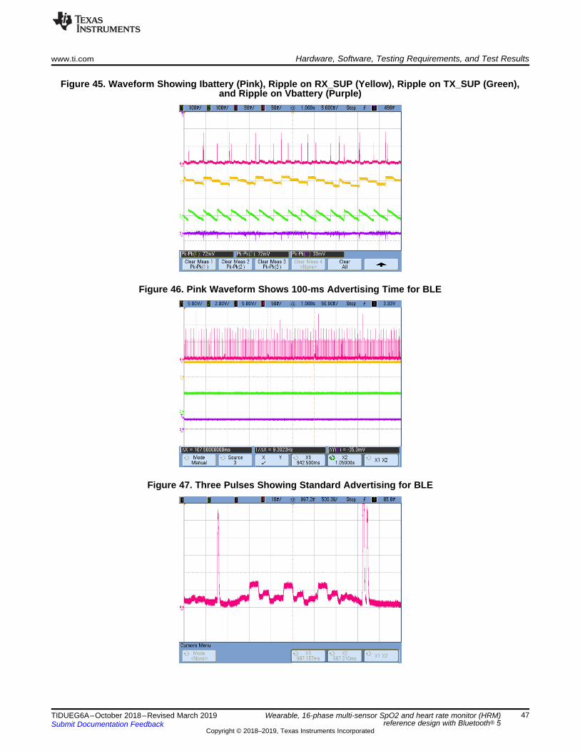
Figure 45. Waveform Showing Ibattery (Pink), Ripple on RX_SUP (Yellow), Ripple on TX_SUP (Green),and Ripple on Vbattery (Purple)
Figure 46. Pink Waveform Shows 100-ms Advertising Time for BLE
Figure 47. Three Pulses Showing Standard Advertising for BLE

Hardware, Software, Testing Requirements, and Test Results www.ti.com
48 TIDUEG6A–October 2018–Revised March 2019Submit Documentation Feedback
Copyright © 2018–2019, Texas Instruments Incorporated
Wearable, 16-phase multi-sensor SpO2 and heart rate monitor (HRM)reference design with Bluetooth® 5
Figure 48. Pulse Showing Standard BLE Once Connected
3.2.2.6 Battery Life TestThe battery life test is done by keeping the TIDA-010029 board on for continuous transmission of the data.The CR3032 battery works continuously for 100 hours.

www.ti.com Design Files
49TIDUEG6A–October 2018–Revised March 2019Submit Documentation Feedback
Copyright © 2018–2019, Texas Instruments Incorporated
Wearable, 16-phase multi-sensor SpO2 and heart rate monitor (HRM)reference design with Bluetooth® 5
4 Design Files
4.1 SchematicsTo download the schematics, see the design files at TIDA-010029.
4.2 Bill of MaterialsTo download the bill of materials (BOM), see the design files at TIDA-010029.
4.3 PCB Layout RecommendationsDevice-specific layout guidelines for each TI part used in this design can be found in the correspondingdata sheets. Figure 49 and Figure 50 show top and bottom views of the TIDA-010029 PCB, respectively.
4.3.1 Layout for Main Board
Figure 49. Top Layer for TIDA-010029 Board

VBATT
VDDR
VBATT
VDDS2/3
TX_SUP
IO_SUP
Design Files www.ti.com
50 TIDUEG6A–October 2018–Revised March 2019Submit Documentation Feedback
Copyright © 2018–2019, Texas Instruments Incorporated
Wearable, 16-phase multi-sensor SpO2 and heart rate monitor (HRM)reference design with Bluetooth® 5
Figure 50. Bottom Layer for TIDA-010029 Board
Figure 51. Power Layer for TIDA-010029 Board

STAR GND point for the
board
GND for CC2640R2F
(Note the vias below IC)
Vias for Antenna Routing
GND plane for AFE4420 and Power
Circuitry
www.ti.com Design Files
51TIDUEG6A–October 2018–Revised March 2019Submit Documentation Feedback
Copyright © 2018–2019, Texas Instruments Incorporated
Wearable, 16-phase multi-sensor SpO2 and heart rate monitor (HRM)reference design with Bluetooth® 5
Figure 52. Ground Layer for TIDA-010029 Board
4.3.2 Connection From PDs to AFE
Figure 53. Traces From PDs to AFE
Design Files www.ti.com
52 TIDUEG6A–October 2018–Revised March 2019Submit Documentation Feedback
Copyright © 2018–2019, Texas Instruments Incorporated
Wearable, 16-phase multi-sensor SpO2 and heart rate monitor (HRM)reference design with Bluetooth® 5
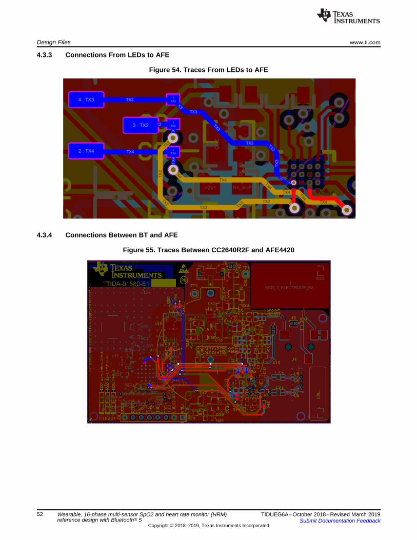
4.3.3 Connections From LEDs to AFE
Figure 54. Traces From LEDs to AFE
4.3.4 Connections Between BT and AFE
Figure 55. Traces Between CC2640R2F and AFE4420

www.ti.com Design Files
53TIDUEG6A–October 2018–Revised March 2019Submit Documentation Feedback
Copyright © 2018–2019, Texas Instruments Incorporated
Wearable, 16-phase multi-sensor SpO2 and heart rate monitor (HRM)reference design with Bluetooth® 5
4.3.5 Connections Between BT Antenna and Chip
Figure 56. Traces Between CC2640R2F and Antenna

Design Files www.ti.com
54 TIDUEG6A–October 2018–Revised March 2019Submit Documentation Feedback
Copyright © 2018–2019, Texas Instruments Incorporated
Wearable, 16-phase multi-sensor SpO2 and heart rate monitor (HRM)reference design with Bluetooth® 5
4.3.6 Boost Converter
Figure 57. Layout and Traces for Boost Converter, TPS61099

www.ti.com Design Files
55TIDUEG6A–October 2018–Revised March 2019Submit Documentation Feedback
Copyright © 2018–2019, Texas Instruments Incorporated
Wearable, 16-phase multi-sensor SpO2 and heart rate monitor (HRM)reference design with Bluetooth® 5
4.3.7 Buck-Boost Converter
Figure 58. Layout and Traces for Buck-Boost Converter, TPS63036

Design Files www.ti.com
56 TIDUEG6A–October 2018–Revised March 2019Submit Documentation Feedback
Copyright © 2018–2019, Texas Instruments Incorporated
Wearable, 16-phase multi-sensor SpO2 and heart rate monitor (HRM)reference design with Bluetooth® 5
4.3.8 Layouts for PPG Sensor Boards
Figure 59. Layout for SFH 7072 Board (Top Layer)

www.ti.com Design Files
57TIDUEG6A–October 2018–Revised March 2019Submit Documentation Feedback
Copyright © 2018–2019, Texas Instruments Incorporated
Wearable, 16-phase multi-sensor SpO2 and heart rate monitor (HRM)reference design with Bluetooth® 5
Figure 60. Layout for SFH 7072 Board (Bottom Layer)

Design Files www.ti.com
58 TIDUEG6A–October 2018–Revised March 2019Submit Documentation Feedback
Copyright © 2018–2019, Texas Instruments Incorporated
Wearable, 16-phase multi-sensor SpO2 and heart rate monitor (HRM)reference design with Bluetooth® 5
4.3.9 Layout PrintsTo download the layer plots, see the design files at TIDA-010029.
4.4 Altium ProjectTo download the Altium project files, see the design files at TIDA-010029 .
4.5 Gerber FilesTo download the Gerber files, see the design files at TIDA-010029.
4.6 Assembly DrawingsTo download the assembly drawings, see the design files at TIDA-010029.
5 Software FilesTo download the software files, see the design files at TIDA-010029.
6 Related Documentation1. Texas Instruments, TINA-TI Simulation Software2. Texas Instruments, Miniaturized Pulse Oximeter Reference Design Getting Started Guide3. Texas Instruments, How to Design Peripheral Oxygen Saturation (SpO2) and Optical Heart Rate
Monitoring (OHRM) Systems Using the AFE4403, application report4. Texas Instruments, Measuring Bluetooth® Low Energy Power Consumption, application report5. Texas Instruments, Measuring Bluetooth Low Energy Power Consumption, application report6. Samah Alharbi, Sijung Hu, David Mulvaney, and Panagiotis Blanos, (February 19, 2018). An applicable
approach for extracting human heart rate and oxygen saturation during physical movements using amulti-wavelength illumination optoelectronic sensor system. Proc. SPIE 10486, Design and Quality forBiomedical Technologies XI, 104860S; doi: 10.1117/12.2287854.
6.1 TrademarksE2E, SimpleLink, TINA-TI, Code Composer Studio are trademarks of Texas Instruments.WEBENCH is a registered trademark of Texas Instruments.Arm, Cortex are registered trademarks of Arm Limited.Bluetooth is a registered trademark of Bluetooth SIG, Inc.LabVIEW is a trademark of National Instruments.OSRAM is a registered trademark of OSRAM Opto Semiconductors GmbH.Wi-Fi is a registered trademark of Wi-Fi Alliance.
6.2 Third-Party Products DisclaimerTI'S PUBLICATION OF INFORMATION REGARDING THIRD-PARTY PRODUCTS OR SERVICES DOESNOT CONSTITUTE AN ENDORSEMENT REGARDING THE SUITABILITY OF SUCH PRODUCTS ORSERVICES OR A WARRANTY, REPRESENTATION OR ENDORSEMENT OF SUCH PRODUCTS ORSERVICES, EITHER ALONE OR IN COMBINATION WITH ANY TI PRODUCT OR SERVICE.

www.ti.com About the Authors
59TIDUEG6A–October 2018–Revised March 2019Submit Documentation Feedback
Copyright © 2018–2019, Texas Instruments Incorporated
Wearable, 16-phase multi-sensor SpO2 and heart rate monitor (HRM)reference design with Bluetooth® 5
7 About the AuthorsSANJAY PITHADIA is a systems designer at Texas Instruments, where he is responsible for developingsubsystem design solutions for the Medical Healthcare and Fitness sector. Sanjay has been with TI since2008 and has been involved in designing reference designs related to energy, smart grid, industrial motordrives, and medical imaging. Sanjay brings to this role his experience in analog design, mixed signaldesign, industrial interfaces, and power supplies. Sanjay earned his bachelor of technology in electronicsengineering at the Veermata Jijabai Technological Institute, Mumbai.
KIRAN RAJMOHAN is a test engineer at Texas Instruments, where he is responsible for testing andcharacterization of high-performance analog IPs like ADC, DAC, PGA, PLL, and RF-signal chains in TImicrocontrollers. Kiran has been with TI since 2015. Kiran earned his bachelor of technology in electronicsand communication engineering at the College of Engineering, Trivandrum, Kerala.

Revision History www.ti.com
60 TIDUEG6A–October 2018–Revised March 2019Submit Documentation Feedback
Copyright © 2018–2019, Texas Instruments Incorporated
Revision History
Revision HistoryNOTE: Page numbers for previous revisions may differ from page numbers in the current version.
Changes from Original (October 2018) to A Revision .................................................................................................... Page
• Changed title of document ............................................................................................................... 1• Changed Description...................................................................................................................... 1

IMPORTANT NOTICE AND DISCLAIMER
TI PROVIDES TECHNICAL AND RELIABILITY DATA (INCLUDING DATASHEETS), DESIGN RESOURCES (INCLUDING REFERENCEDESIGNS), APPLICATION OR OTHER DESIGN ADVICE, WEB TOOLS, SAFETY INFORMATION, AND OTHER RESOURCES “AS IS”AND WITH ALL FAULTS, AND DISCLAIMS ALL WARRANTIES, EXPRESS AND IMPLIED, INCLUDING WITHOUT LIMITATION ANYIMPLIED WARRANTIES OF MERCHANTABILITY, FITNESS FOR A PARTICULAR PURPOSE OR NON-INFRINGEMENT OF THIRDPARTY INTELLECTUAL PROPERTY RIGHTS.These resources are intended for skilled developers designing with TI products. You are solely responsible for (1) selecting the appropriateTI products for your application, (2) designing, validating and testing your application, and (3) ensuring your application meets applicablestandards, and any other safety, security, or other requirements. These resources are subject to change without notice. TI grants youpermission to use these resources only for development of an application that uses the TI products described in the resource. Otherreproduction and display of these resources is prohibited. No license is granted to any other TI intellectual property right or to any thirdparty intellectual property right. TI disclaims responsibility for, and you will fully indemnify TI and its representatives against, any claims,damages, costs, losses, and liabilities arising out of your use of these resources.TI’s products are provided subject to TI’s Terms of Sale (www.ti.com/legal/termsofsale.html) or other applicable terms available either onti.com or provided in conjunction with such TI products. TI’s provision of these resources does not expand or otherwise alter TI’s applicablewarranties or warranty disclaimers for TI products.
Mailing Address: Texas Instruments, Post Office Box 655303, Dallas, Texas 75265Copyright © 2019, Texas Instruments Incorporated


![In-Ear SpO2: A Tool for Wearable, Unobtrusive Monitoring of … · 2020. 6. 8. · SpO 2 readings are a sign of hypoxia without breathlessness in COVID-19 patients [4] [5] where the](https://static.fdocuments.net/doc/165x107/60d734c91438265ecd1571c7/in-ear-spo2-a-tool-for-wearable-unobtrusive-monitoring-of-2020-6-8-spo-2.jpg)


