
000 TEL 0476 (22) 2111 · 000 TEL 0476 (22) 2111 . 60 ffÐ0 1 99 . Created Date: 5/15/2019 4:58:43 PM
Upload
phungkhanhCategory
view
214download
0
Final Technical Report
Contract AFOSR F4962096-1-0476 9/30/96-9/30/98
Monitored by Dr. Alan Craig
"WDM Laser Sources for the Defense University (Testbed) Research Internet Program (DUTRIP)"
TTU Account No. 1303-44-4608
Texas Tech University Department of Electrical Engineering
Lubbock, Texas 79409
PI: Henryk Temkin Office: (806) 742-1264
Email: [email protected]
January 31, 1999
©TIC QUALITY INSPECTED 8 20000509 040

REPORT DOCUMENTATION PAGE AFRL-SR-BL-TR-OO-
tato««taO|>»roti«oriJF«*orM215JoHori«iDM» 222024302. aid to *• Met of MMQM«
rBEFinsnMOTnsmsTswrar i. A6E^VUiEÖNL^l««to7*y LKPöRTDATE
Final30Sep96to30Sep98 4. TITLE AND SUBTITLE WDM Laser sources for the defense university (Testbed) Research internet program
(Bmdo-Durip)
6. AUTHORISI
Professor Temkin
7. PERFORMING ORGANIZATION NAME(S) AND ADDRESS(ES)
Texas Tech University 203 Holden Hall LubbockTX 79409-1035
9. SPONSORING/MONITORING AGENCY NAME(S)AND ADDRESSIES)
AFOSR/NE 801 N Randolph Street Rm 732 Arlington, VA 22203-1977
5. FUNDING NUMBERS
61103D 3484/US
8. PERFORMING ORGANIZATION REPORT NUMBER
10. SPONSORING/MONITORING AGENCY REPORT NUMBER
F49620-96-1-0476
il. SUPPLEMENTARY NOTES
12«. DISTRIBUTION AVAILABIUTY STATEMENT
APPROVAL FOR PUBLIC RELEASE, DISTRIBUTION UNLIMITED
13. ABSTRACT (Uumtm 200 wards/
12b. DISTRIBUTION CODE
These specification were discussed with a number of vendors. Ortel Corporation was identified as a low cost supplier capable of satisfying all of the above specifications. Ortel Corporation fabricated and delivered 52 arrays of WDM lasers, each operating at four wavelengths, as specified above. We have established a testing metholdology for these WDM arrys and conducted extensive test. The results are summarizec in an attached paper, presented at the 1999 SPIE Photonics West in San Jose.
14. SUBJECT TERMS
17. SECURITY CLASSIFICATION OF REPORT
UNCLASSIFIED
18. SECURITY CLASSIFICATION OF THIS PAGE
UNCLASSIFIED
19. SECURITY CLASSIFICATION OF ABSTRACT
UNCLASSIFIED
15. NUMBER OF PAGES
18. PRICE CODE
{
lib. LIMITATION ÖF At&TAAöTl
UL
Mpmd uw« Porfon Pro, WHS/BOP, Oet 04

Final Technical Report
Contract AFOSR F4962096-1 -0476 9/30/96-9/30/98
"WDM Laser Sources for the Defense University (Testbed) Research Internet Program (DUTRIP)"
I. Research
The objective of this project was to define specifications of a hybrid integrated
wavelength division multiplexed laser source, to identify the appropriate vendor, and to
negotiate an acceptable price structure.
II. Design Specifications
In consultation with a number of user groups and the DUTRIP program at University of
Maryland (PI: Prof. Mario Dagenais) we have determined the following set of
specifications for the four wavelength WDM array:
1) Emission wavelengths of DFB lasers:
channel 1: 1549.32 nm
channel 2: 1552.52 nm (the reference of 193.1 THz.)
channel 3: 1555.75 nm
channel 4: 1558.99 nm
All channel wavelengths to be accurate to ± 0.3 nm*
2) SMSR > 30 dB under 40 mA peak-to-peak modulation and 8.2 dB extinction
ratio (SONET OC-48 spec.)
3) Threshold current < 30 mA
4) External efficiency >0.2 mW/raA
5) Fundamental transverse mode operation up to IDC =100 mA
6) Power coupled into >+6.0dBm
single mode fiber @100 mA
7) Modulation bandwidth 2.5 Gb/s **

8) Four ECL inputs to drivers: ECL, 50 Q
9) Four single mode outputs, optical isolator in each laser package.
10) Back facet monitor in each laser package
11) Front panel setting of laser bias current and temperature for each laser.
12) Front panel indicator lights to indicate operation of each laser
* All wavelengths and spectral properties measured at a chip power output of 5 mW. The
wavelength may be trimmed with a TC cooler, as long as other specs are maintained
** modulation bandwidth is limited by the driver chip.
Additional Considerations The vendor will (a) provide available test and reliability data, and (b) establish the device code and make it available to other customers at a fixed price
III. Results These specifications were discussed with a number of vendors. Ortel Corporation was
identified as a low cost supplier capable of satisfying all of the above specifications. Ortel
Corporation fabricated and delivered 52 arrays of WDM lasers, each operating at four
wavelengths, as specified above. We have established a testing methodology for these
WDM arrays and conducted extensive test. The results are summarized in an attached
paper, presented at the 1999 SPIE Photonics West in San Jose.
We have investigated wavelength accuracy and stability of WDM transmitters
delivered to us by Ortel Corporation. Transmitter performance was tested under DC bias
and modulation at data rates as high as 2.5Gbps. The wavelength accuracy of hybrid
devices was found to be considerably better than +0.1nm. A considerable fraction of
devices tested showed small wavelength, less than 0.02 nm, and power, less than 0.1 dB,
excursions due to digitization noise of control circuitry. Transmission experiments
through 100 km of standard single mode fiber show low chirp penalties and, in case of
monolithic arrays, the absence of cross-talk. Long term transmission experiments, up to
1000 hrs, through wavelength-selective elements simulating WDM systems do not show

any penalties due to the wavelength or power instabilities. All the devices tested in our
experiments are suitable for WDM systems research. This work has allowed us to,
conclude that the transmitters delivered by Ortel met or exceeded our specifications.
In order to facilitate testing we have constructed a number of test-beds, some of
which included passive devices such as multiplexers and demultiplexers. These passive
devices had to be independently characterized. In the process we realized that the current
modeling of passive devices could be considerably improved.
The design of waveguide components and optical circuits, requires detailed
knowledge of light-guiding parameters, field distributions, transfer -efficiencies, etc., in
complex device structures and devices coupled into systems. Much of the previous work
done in this field concentrated on two aspects of this problem. First, several powerful
methods have been developed to evaluate eigenvalues and eigenfunctions for specific
waveguide structures. These are the finite-difference or multi-grain method, the finite-
element or variational method, the effective index methods, the boundary element or
integral-equation method and the specific matrix implementation of it known as the
Galerkin method, the WKB method, numerous numerical methods, etc.
Second, after the eigenvalues and eigenfunctions are calculated, their propagation
through an optical circuit must be accounted for. The propagation aspects makes the
calculation of field distributions a complicated and time-consuming task. Much of the
past effort has been devoted to the computation of field distributions and propagation
characteristics of waveguide devices in which optical energy couples between the input
and output ports. The best known examples are the work of Dragone, and Henry and
coworkers, who used finite Fourier transform propagation method. Very little attention
has been given in the past to coupling between waveguides and free space optics.
The previous work usually considered field distributions in optical waveguide
structures in terms of scalar electrodynamics. However, the pioneering work on radar,

antennas and microwave waveguides, has demonstrated the general usefulness of
describing electromagnetic fields in terms of vector electrodynamics. The significance of
this comes from the fact that the optical waveguide systems are described not only by the
wave equation for the fields, but also by the boundary conditions which are vectorial in
nature. Moreover, in optoelectronic devices the distribution of polarization, a vector-like
quantity, must also be considered. Consequently, a vectorial formulation might be
expected to have an advantage in computation and design of optical waveguide systems
and in modeling of the interface between waveguides and free space.
We have developed a new transfer-amplitude method to describe field
distributions and efficiencies of optical waveguide systems based on vector
electrodynamics. The starting point of the analysis is Huygens' picture of propagation of
time-harmonic electromagnetic fields in complex waveguide structures as expressed by
Love's formulation ( A. E. H. Love, Phil Trans. Royal Soc. London A, v. 197, pp. 1-45,
1901) of the vectorial Green's theorem. This approach allows us to divide a complex
optical waveguide structure into a set of primitive blocks and calculate a transfer
amplitude and a transfer function for each block separately. We demonstrate that Love's
expressions for equivalent surface current densities lead to correct results for the field
distributions in primitive blocks. It is then possible to calculate partial and total transfer
functions and corresponding device efficiency with high accuracy.
The representation of a complex waveguide structure by a set of principal surfaces
separating primitive blocks with known equivalent surface currents and propagation
functions was shown to be a very useful method. This method provides a possibility of
constructing the total system response as a convolution of responses of its primitive
blocks. It is a very close analogue of the method of geometrical optics with its principal
surfaces and primitive blocks. The distinction is that an exact propagation function,
including diffraction effects, is used here to describe each primitive block, instead of the
simple ray approximation. These ideas were already applied to the evaluation of
Dragone's router, a waveguide problem of considerable complexity. These ideas can be

also applied to modeling of 3D problems which include both waveguide and free space
propagation, eg. coupling of lasers, with an arbitrary far field distribution, to fibers
through lenses and lens systems. The model will include arbitrary source polarization and
will allow for calculating the sensitivity of coupling efficiency to component
misalignment.
Two papers describing these ideas in detail are attached to this report.
IV. Personnel
Henryk Temkin, Professor, Principal Investigator
D. V. Kuksenkov, Senior Research Associate, now with Corning Inc, irreorning NY.

Hybrid and Monolithic Wavelength Division Multiplexed Transmitter Arrays: Performance of Commercially Available Devices
G. Guidice and H. Temkin, Department of Electrical Engineering, Texas Tech University, Lubbock, TX 79409
Hongbo Wang, Guoxi Sun, Zhencan Frank Fan and M. Dagenais Department of Electrical Engineering, University of Maryland, College Park, MD 20742
Yung Jui Chen Department of Computer and Electrical Engineering, University of Maryland
Baltimore County, Ellicott City, MD 21042
M. Fallahi, D.L. Mathine and N. Peyghambarian Optical Sciences Center, University of Arizona, Tucson, AZ 85721
Abstract
This paper reviews performance of hybrid and monolithically integrated WDM transmitter arrays based on directly modulated 2.5Gbps lasers, with a focus on the wavelength accuracy and stability under normal operating conditions. We also consider power stability, chromatic dispersion penalties, and the channel cross-talk. Large numbers of four-wavelength devices were obtained and evaluated under a program designed to provide university-based system researchers with advanced WDM components We show that multi-wavelength laser arrays capable of high-performance out-of-the-box operation can be now produced for research-type WDM systems.
Introduction
Multiple-wavelength laser sources are the fundamental component of WDM systems and considerable research and development effort has been devoted to their design and fabrication. The research effort, in particular, has focused on monolithically integrated multiple-wavelength laser arrays, widely believed to be a superior source, particularly in applications involving many wavelengths. However, while practically all of current commercial WDM systems rely on discrete lasers with pre-selected wavelengths, properties of such hybrid-integrated sources remain poorly documented. This divergence of research and industrial practice underscores the difficulty of producing stable, monolithic, multiple-wavelength arrays capable of meeting WDM system requirements. However, with WDM systems moving towards higher channel density and higher bit rates the virtues of the hybrid vs the monolithic approach need to be reassessed.
In the design of multiple wavelength laser arrays, either hybrid or monolithic, one has to consider a range of issues:
• Gain material: a typical WDM system has a 20 to 30 nm operating range in the 1.55 micron region which is defined by the Er-doped fiber amplifier (EDFA) gain window. Lasers based on quantum well structures that exhibit continuously tunable gain region of more than 200 nm might be the structures of choice [1]. More recently, there has

been also increasing interest in the use of fiber lasers in WDM applications, as their gain matches that of the EDFA [2]. Wavelength tuning/locking: High quality laser sources can be readily produced using a distributed feedback grating (DFB) or a distributed Bragg reflector structure [3]. Currently most semiconductor laser arrays utilize DFB structures. With increasing number of WDM channels, the channel spacing becomes smaller and the wavelength registration accuracy requirements become more stringent. Current dense-WDM systems call for channel spacing of 50 GHz, with a GHz wavelength accuracy. In order to operate such laser arrays under different environmental and operating conditions, careful control of the temperature [4] and power are required. A number of laser designs incorporating additional build-in electrodes for wavelength tuning have been proposed [5]. In a sampled grating configuration [5a], more than 60 nm tuning was demonstrated. Wavelength stabilization through external frequency-selective feedback, provided through an external bulk grating, fiber grating, or a WDM demultiplexer, is also being investigated [6]. In addition, active frequency locking using solid state etalons, or other types of wavelength lockers, is under study for the long term wavelength stabilization of single and multiple-frequency laser sources [6a]' Power combining: The use of simple 3 dB couplers to combine to combine 2 laser sources results in the power loss, for each laser, of Nx 3 dB\ With the use of a star coupler the loss is still 10 x logN. In a 40 channel WDM system, this amounts to a loss of 16 dB! As the channel number increases, it becomes desirable to use wavelength multiplexers to combine the outputs of a multiple wavelength source. The typical interference filter or fiber grating WDM multiplexer for 8 to 16 channels has a fiber to fiber loss of 2-3 dB. As the channel count increases, both the insertion loss and the cost of multiplexers increase rapidly. For large channel count applications integrated WDM multiplexers, such as arrayed waveguide grating (AWG), become a viable choice [7]. The 16-channel AWG typically have a fiber-to-fiber insertion loss of 4-6 dB and the loss increases only slightly for larger channel counts. However, impressive research results to the contrary, such devices cannot be readily incorporated into a monolithic array. The optical feedback is another serious issue related to power combining. While dealing with discrete lasers, one can use isolators to eliminate the optical feedback. However, isolators suitable for integrated laser arrays, in particular high channel- count laser arrays, simply do not exist and the optical feedback remains a very difficult problem. Data modulation: Current WDM systems operate at 2.5 Gbps and the data rate is
moving toward 10 Gbps. To provide high quality optical signal at 2.5 Gbps and higher rates, the data should be encoded through external modulation. For individual lasers, and hybrid WDM sources, this can be readily accomplished via external EO modulators. To modulate integrated laser arrays, a monolithically integrated on-chip modulator is desirable. There has been considerable progress on integrating electroabsorption modulators with DFB lasers [9, 9a]. Electronic laser driver arrays have also been demonstrated at data rate of 2.5 Gbps and beyond [10,10a]. In hybrid integration of electronic driver chips to a laser array, via wire bonding, electrical cross-talk can be an issue.

The early integrated multiple-wavelength arrays were based on DFB and DBR two- section lasers allowing for electrical tuning [11-12]. Large laser arrays were made based on bulk [13] and strained quantum well [14-16] active layer structures. The strained structures produce lower threshold lasers with narrow linewidth and lower thermal crosstalk. These devices required either high resolution lithography to produce the proper DFB grating pitch or needed repeated holographic exposures [12]. Introduction of the phase mask was a major advancement in the lithographic mask definition [19]. E-beam lithography was also used to prepare highly accurate gratings with fine pitch shifts. To further adjust the wavelength, individual on-chip heaters were introduced [17-18].
Early WDM experiments combined the output of laser arrays into a single fiber with the use of elaborate bulk multiplexers [20]. Miniature diffraction gratings and hybrid micro-optics were introduced to simplify this process [21]. An on-chip power combining element for a three-laser array was first reported by Koren et al. [12]. An integrated optical amplifier was also provided to compensate for the combiner loss. An NxM star coupler was later used to combine the output power of a 20-wavelength laser array [22]. In a separate effort, electroabsorption modulators were inserted between the lasers and the star coupler to permit high data-rate modulation of individual lasers [23]. In both cases, an optical amplifier at the output was used to compensate for the power loss.
Although WDM multiplexer is a more efficient power combiner for a large channel- count laser array, it is quite difficult to match the MUX passband to the laser wavelength in a monolithic chip. However, the MUX can be used as a wavelength locker to generate multiple wavelength outputs. The MAGIC (multistripe array grating integrated cavity) laser [24] was the first demonstration of this concept utilizing a curved mirror grating as the wavelength selective element. The MAGIC laser not only produces multiple wavelength output, it also combines them into a single output channel [25]. The wavelength locking idea was also implemented with the arrayed waveguide grating (AWG) WDM multiplexer [26-29]. The multi-wavelength router laser can be also used as a tunable laser source. A digitally tunable laser source with build-in electroabsorption modulator has also been reported [31-32].
Finally we note the wavelength selectable fiber ring lasers using Er-doped fiber amplifier as the gain medium and an AWG for wavelength selection [2, 33]. Since the laser cavity is long, there are typically 103 to 104 axial modes within the 3 dB passband of the AWG. The laser can potentially operate multimode and thus introduce excess intermodal optical beat noise. A recent paper reported the use of a semiconductor Fabry- Perot optical amplifier as an intracavity narrow band filter to stabilize laser oscillation in a single axial mode [34].
Experimental Results
The hybrid integrated laser sources used in this work were provided by the Ortel Corp (transmitter model 10348A). The design goal was to produce two four-wavelength sources, each on an ITU grid of 3.2 nm (400 GHz), with the shortest reference wavelength of 1549.32 nm and 1550.92 nm respectively for each WDM source. Two such sources can be easily combined into an eight wavelength source or a source operating on a 200 GHz grid with wavelengths varying from 1549.32 to 1560.61 nm. Each transmitter module consisted of four independent plug-in units, each containing an

ECL compatible laser driver, a distributed feedback laser, an optical isolator, and an FC/PC fiber optic connector. Individual lasers were independently temperature and power controlled. LED indicators were provided to indicate the status of control circuitry. At the operating point, the fiber-coupled power output from each lasers was set to be greater than 2 mW. Four separate plug-ins were inserted into a rack mountable chassis to provide a DC power supply for the necessary bias voltages to each transmitter. Over one hundred such transmitters were delivered and tested.
The monolithically integrated laser arrays were obtained from Nortel Corp. Each source consisted of a monolithic four-wavelength laser array fiber-pigtailed to an array of 4 single-mode fiber. The light from the 4-laser array was simultaneously imaged through an optical system composed of 3 successive lenses and a single optical isolator. An ECL compatible laser driver was used to drive the laser at 2.5 Gbps. The laser array was mounted on a single temperature controller, with a single control circuit for the four laser array.. The fiber-pigtailed power in each fiber is more than 1 mW. The wavelength of the laser array varied between 1552.52 to 1557.36 nm in steps of 200 GHz. The DC bias current for each laser could be controlled individually.
E CO ■o
CO c CD c
0-
-10
<=- -20
-30
-40
-50
-60 1540 1545 1550 1555 1560
Wavelength (nm)
1565
Fig. 1A set often spectra obtained from hybrid four-laser WDM sources provided by the Ortel Corporation.
WDM laser transmitter modules were tested for wavelength and power stability. For the initial DC testing of hybrid arrays, light output from individual lasers was combined using a commercial 1 x 4 combiner, displayed on an optical spectrum analyzer with a resolution of 0.8 A, and stored in a computer. A spectrum from each array was obtained after a five minutes warm-up time, to allow the power and temperature control circuits to stabilize. All the arrays were tested directly after shipment from the manufacturer,
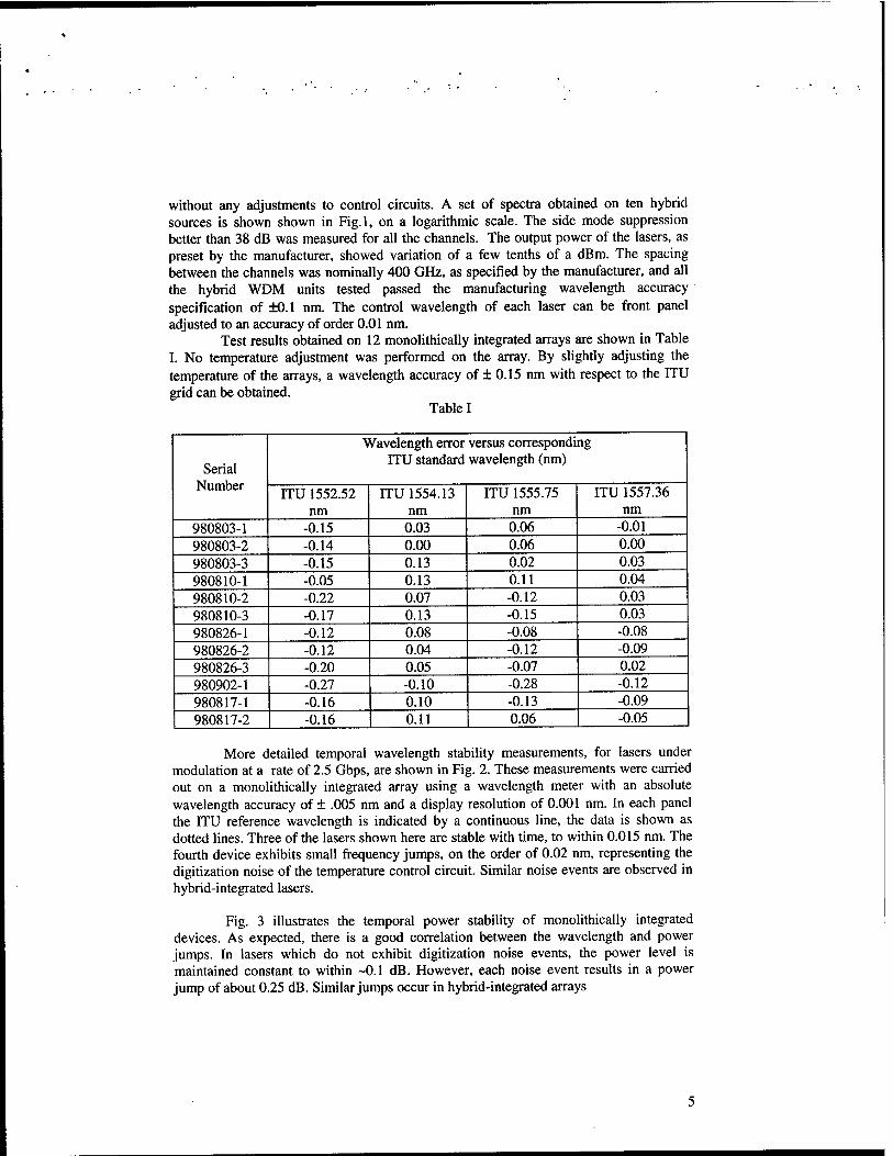
without any adjustments to control circuits. A set of spectra obtained on ten hybrid sources is shown shown in Fig.l, on a logarithmic scale. The side mode suppression better than 38 dB was measured for all the channels. The output power of the lasers, as preset by the manufacturer, showed variation of a few tenths of a dBm. The spacing between the channels was nominally 400 GHz, as specified by the manufacturer, and all the hybrid WDM units tested passed the manufacturing wavelength accuracy specification of ±0.1 nm. The control wavelength of each laser can be front panel adjusted to an accuracy of order 0.01 nm.
Test results obtained on 12 monolithically integrated arrays are shown in Table I. No temperature adjustment was performed on the array. By slightly adjusting the temperature of the arrays, a wavelength accuracy of ± 0.15 nm with respect to the ITU grid can be obtained.
Table I
Serial Number
Wavelength error versus corresponding ITU standard wavelength (nm)
ITU 1552.52 nm
ITU 1554.13 nm
ITU 1555.75 nm
ITU 1557.36 nm
980803-1 -0.15 0.03 0.06 -0.01 980803-2 -0.14 0.00 0.06 0.00 980803-3 -0.15 0.13 0.02 0.03 980810-1 -0.05 0.13 0.11 0.04 980810-2 -0.22 0.07 -0.12 0.03 980810-3 -0.17 0.13 -0.15 0.03 980826-1 -0.12 0.08 -0.08 -0.08 980826-2 -0.12 0.04 -0.12 -0.09 980826-3 -0.20 0.05 -0.07 0.02 980902-1 -0.27 -0.10 -0.28 -0.12 980817-1 -0.16 0.10 -0.13 -0.09 980817-2 -0.16 0.11 0.06 -0.05
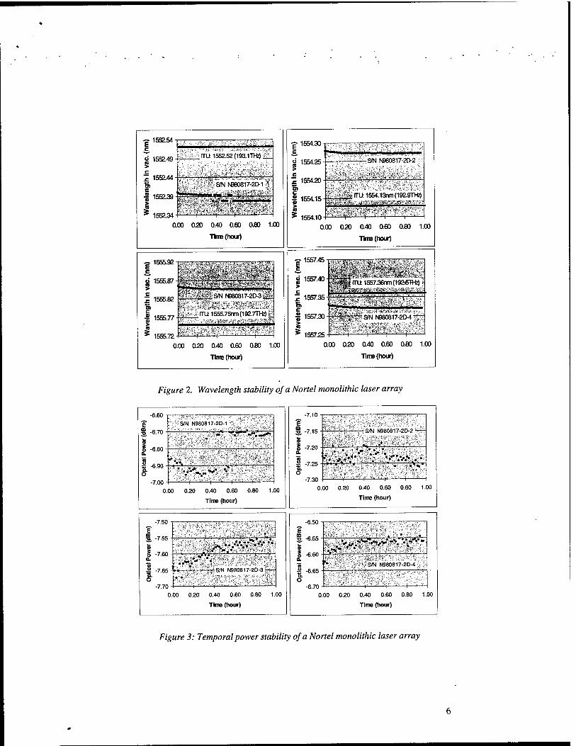
More detailed temporal wavelength stability measurements, for lasers under modulation at a rate of 2.5 Gbps, are shown in Fig. 2. These measurements were carried out on a monolithically integrated array using a wavelength meter with an absolute wavelength accuracy of ± .005 nm and a display resolution of 0.001 nm. In each panel the ITU reference wavelength is indicated by a continuous line, the data is shown as dotted lines. Three of the lasers shown here are stable with time, to within 0.015 nm. The fourth device exhibits small frequency jumps, on the order of 0.02 nm, representing the digitization noise of the temperature control circuit. Similar noise events are observed in hybrid-integrated lasers.
Fig. 3 illustrates the temporal power stability of monolithically integrated devices. As expected, there is a good correlation between the wavelength and power jumps. In lasers which do not exhibit digitization noise events, the power level is maintained constant to within -0.1 dB. However, each noise event results in a power jump of about 0.25 dB. Similar jumps occur in hybrid-integrated arrays
0.00 050 0.40 0.60 0.80 1.00
Time (hour)
.=. 1555.92 c
155587" s^i^^a^feliBii 1555.82
O) c a % 5
S 1555.77
1555.72
1M&NN980817-2D-3I
j IRJt 1555.75nm (192.7THz) jig
-H -H^
0.00 050 0.40 0.60 0.80 1.00
Time (hour)
1554.30
1554.25
1554.20
1554.15
1554.10
iSN N980817-2D-2 ~
Wm ITU 1554.13nm(192.9THz)
^ 0.00 050 0.40 0.60 0.80 1.00
Time (hour)
1557.45
1557.40
1557.35
1557.30
1557.25
§P£§i ITU 1557.36nm (192«THz)
gSWM N980817-2O4J
0.00 0.20 0.40 0.60 0.80 1.00
Time (hour)
Figure 2. Wavelength stability of a Nortel monolithic laser array
B
s. -6-70 ■ a o -6.80 - o- n = -6.90 - £L O
iS/N N980817-2D-1 %^
m '•J-.'m*^
'• '*. . ••/■%,•.■*■ -V i;?:i*Si&:
0. 00 0.20 0.40 0.60
Time (hour)
0.80 1. 00
E S -7.55
I -7.65 o. O
-7.70
, , . ..
7m
SS/N N980817-2D-3"
0.00 0.20 0.40 0.60 0.80 1.00
Time (hour)
-7.10 ? GQ S. -7.15
I -7.25
JS/N N980817-2D-2 «
m
0.00 0.20 0.40 0.60 0.80 1.00
Time (hour)
-6.50 ? S -6.55
I -6.60 a.
I -6.65 »S/N N980817-2D-4 *
0.00 0.20 0.40 0.60 0.80 1.00
Time (hour)
Figure 3: Temporal power stability of a Nortel monolithic laser array
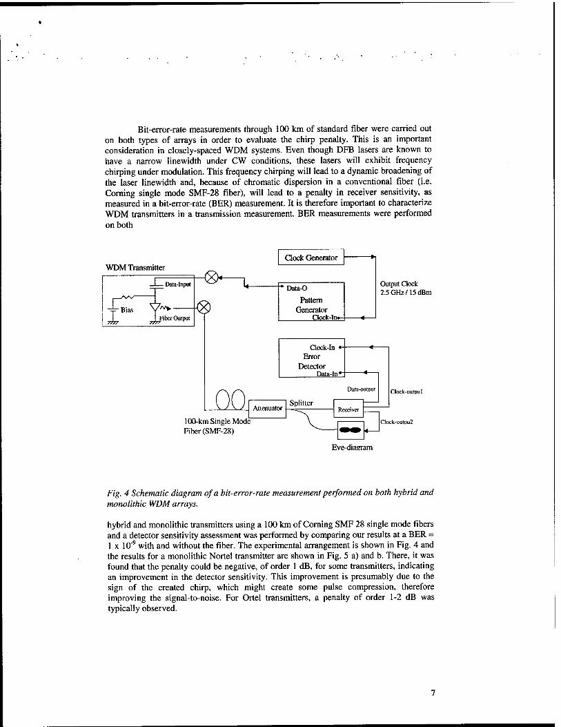
Bit-error-rate measurements through 100 km of standard fiber were carried out on both types of arrays in order to evaluate the chirp penalty. This is an important consideration in closely-spaced WDM systems. Even though DFB lasers are known to have a narrow linewidth under CW conditions, these lasers will exhibit frequency chirping under modulation. This frequency chirping will lead to a dynamic broadening of the laser linewidth and, because of chromatic dispersion in a conventional fiber (i.e. Corning single mode SMF-28 fiber), will lead to a penalty in receiver sensitivity, as measured in a bit-error-rate (BER) measurement. It is therefore important to characterize WDM transmitters in a transmission measurement. BER measurements were performed on both
WDM Transmitter Clock Generator
■ Data-Input
1 Bias V//vy.
j Fiber Output
■<gx- * Data-O
Pattern Generator Clock-In»
Output Clock 2.5GHz/15dBm
Clock-In •■ Error
Detector Data-in *"
Data-outDut
Attenuator
100-km Single Mode Fiber (SMF-28)
Splitter Receiver
Clock-outpul
Clock-outou2
Eve-diagram
Fig. 4 Schematic diagram of a bit-error-rate measurement performed on both hybrid and monolithic WDM arrays.
hybrid and monolithic transmitters using a 100 km of Corning SMF 28 single mode fibers and a detector sensitivity assessment was performed by comparing our results at a BER = 1 x 10"9 with and without the fiber. The experimental arrangement is shown in Fig. 4 and the results for a monolithic Nortel transmitter are shown in Fig. 5 a) and b. There, it was found that the penalty could be negative, of order 1 dB, for some transmitters, indicating an improvement in the detector sensitivity. This improvement is presumably due to the sign of the created chirp, which might create some pulse compression, therefore improving the signal-to-noise. For Ortel transmitters, a penalty of order 1-2 dB was typically observed.

BER Property of Nortel Transmitter 980817-1-1 (No Fiber vs 100km Fiber)
1.0E-02
1.0E-03
1.0E-04
1.0E-05
1.0E-06
1.0E-07
1.0E-08
1.0E-09
1.0E-10 1.0E-11 1.0E-12
-38 -37 -36 -35 -34 -33 -32 -31 -30
Fig. 5 Transmission experiment evaluating the chirp penalty of a monolithic WDM transmitter array
Crosstalk Property of Nortel Transmitter 980817-1 (100km Fiber) 1.0E-02
1.0E-03
« 1.0E-04
W 1.0E-05
00 1.0E-06
1.0E-07
1.0E-08
1.0E-09
1.0E-10 1.0E-11 1.0E-12
,
< > jk. Läse
n riN-a A. nee
-40 -39 -38 -37 -36 -35 -34
Received Power (dBm)
-33 -32
Figure 6. Crosstalk measurement on a Nortel monolithic laser array

The possibility of laser-to-laser interactions, cross-talk, might be of some concern in monolithically integrated devices. Fig. 6 shows the results of a transmission experiment designed to evaluate the degree of cross talk. The transmission experiment measured the bit error rate as a function of received power, through 100 km of fiber. The experiment was first carried out with the modulation applied only to one of the lasers, laser #1, and then repeated with both lasers #1 and #2 under modulation. The presence of cross talk would normally result in a bit-error-rate-penalty, i.e. it would produce a shift between the two lines. The experiment illustrated in Fig. 6 shows that such a penalty is indeed very small in the monolithic array and is less than 0.1 dB, of no consequence in most transmission experiments of interest. This degradation mode is absent in hybrid- integrated devices.
Fiber Spool Waveguide Router
BER Measurement
Fig. 7 Long term, 1000 hrs, transmission experiment through a waveguide router. There were no errors attributable to wavelength or power instabilities.
The final experiment, Fig. 7, illustrates performance of our lasers in a test WDM system. In this experiment the laser output from a hybrid array was first combined into a single fiber and connected to 100 km spool. The fiber was then attached to a 5 x 5 waveguide grating router used as a de-multiplexer. The router is capable of wavelength discrimination greater than 30 dB and a offers a bandpass of -0.5.nm. Any variation in the laser output outside the bandpass of the router would result in catastrophic error rates. A receiver was then connected to the center output waveguide and the received power was adjusted to produce a bit-error-rate of 1E-9. The laser was modulated at a rate of 2.5
Gbps. The setup was allowed to run for 1000 hours and a log of BER measurements was accumulated under computer control. The highest BER recorded in that period was 6E-9.
Summary
We have investigated wavelength accuracy and stability of commercially available WDM transmitters. Large numbers of hybrid and monolithically integrated sources were tested as-delivered from manufacturers. Transmitter performance was tested under DC bias and modulation at data rates as high as 2.5Gbps. The wavelength accuracy of hybrid devices was found to be considerably better than ±0.1 nm. A considerable fraction of devices tested showed small wavelength, less than 0.02 nm, and power, less than 0.1 dB, excursions due to digitization noise of control circuitry. Transmission experiments through 100 km of standard single mode fiber show low chirp penalties and, in case of monolithic arrays, the absence of cross-talk. Long term transmission experiments, up to 1000 hrs, through wavelength-selective elements simulating WDM systems do not show any penalties due to the wavelength or power instabilities. The commercial devices tested in our experiments are suitable for WDM systems research.
Acknowledgements This project was made possible by the vision and enthusiastic support of Lou Lome of BMDO and Alan Craig of AFOSR. They were also instrumental in guiding the project to a successful conclusion. Many thanks are also due to Deborah Crawford at NSF for her support and advice. Finally, we would like to thank Siamak Forouhar of JPL for his patience and many useful conversations.
References
1. M. Bagley, R. Wyatt, D. J. Elton, H. J. Wickes, P. C. Spurdens, C. P. Seltzer, D. M. Cooper, W. J. Devlin, "242nm continuous tuning from a GRIN-SC-MQW- BH InGaAsP laser in an external cavity", Electron. Lett. 26, pp. 267-269, 1990
2. H. Takahashi, H. Toba and Y. Inoue, "Multiple wavelength ring laser composed of EDFA's and an arrayed-waveguide wavelength multiplexer", Electron. Lett. 30, pp. 44-45, 1994
3. H. Kogelnik and C. V. Shank, "Coupled-wave theory of distributed feedback lasers", J. Appl. Phys. Vol. 43, pp. 2327-2334, 1972
4. L. A. Wang, Y. H. Lo, A.S. Gozdz, P. S. D. Lin, M. Z. Iqbal, and R. Bhat, "Integrated four-wavelength DFB laser array with 10 Gb/s speed and 5 nm continuous tuning range", IEEE Photon. Technol. Lett. 4, 318-320, 1992
5. U. Koren, T. L. Koch, B I. Miller, G. Eisenstein, and B. H. Bosworth, "Wavelength division multiplexing light source with integrated quantum well tunable lasers and optical amplifiers", Appl. Phys. Lett., 54, 2056-2058, 1989
5a. "Diode Lasers and Photonics Integrated Circuits", L.A. Coldren and S.W. Corzine, (Wiley, New York, 1995) pp. 350-353.
6. I. H. White, K. O. Nyairo, P. A. Kirkby, and C. J. Armistead, "Demonstration of a 1 x 2 multichannel grating cavity laser for wavelength division multiplexing (WDM) applications," Electron. Lett., vol. 26, pp. 832-834, 1990.
6a. Y.C. Chung and L.W. Stulz, "Synchronized etalon filters for standardizating WDM transmitter laser wavelengths", IEEE Photon. Tech. Lett. 5, 186-189 (1993)
10

7. M. K. Smit and C. Van Dam, "PHASAR-based WDM-devices: principles, design and applications," IEEE J. on Selected Topics in Quantum Electronics, Vol. 2, pp. 236-250, 1996
9. T. Tanbun-Ek, R. People, T. Fullowan, C. Bethea, A. M. Sergent, P. W. Wisk, P.F. Sciortino, Jr., S. N. G. Chu, and W. T. Tsang, IEEE Photonics Tech. Lett., vol 7, no. 7, pp697-699, July 1995
9a. D. M. Adams, C. Rolland, J. Yu, D. Melville, S. Bradshaw, H.B. Kim, F. Shephard, N. Puetz, and B. Richardson, "Gain Coupled DFB Integrated with a Mach-Zehnder modulator for 10 Gbit/s transmission at 1.55 urn over NDSF", in SPffi, vol. 3038, p.45 (1997).
10. K. D. Pedrotti, F. Zucca, P. Zampardi, K. Nary, S. Beccue, K. Liunge, D. Meeker, J. Penny and K. C. Wang, "HBT transmitter and data regenerator arrays for WDM optical communication applications", Proc. GaAs IC Sympos. Philadelphia, PA, pp.197-200, Oct. 1994
10a. David J. Copeland, S. Ahmad Tabatabaei, Scott A. Merritt, Mario Dagenais, Stephen Didde, Ray Y.J. Chen, Dennis Stone, Anthony J. Springthorpe, "Development and Performance of a 40 Gbs WDM Laser Module", SPJE Vol. 3234, pp54-63 (1997).
11. H. Yasaka, J. Nakano, M. Fukuda, Y. Nakano, and Y. ltaya, "Optical frequency spacing tunable four-channel integrated 1.55 urn multielectrode distributed- feedback laser array," IEEE Photon. Technol. Lett., vol.1, pp.75-76, Apr. 1989.
12. U. Koren, T. L. Koch, B. I. Miller, G. Eisenstein, and K. H. Bosworth, "wavelength division multiplexing light source with integrated quantum well tunable lasers and optical amplifiers." Appl. Phys. Lett., vol.54, pp.2056-2058, May, 1989
13. M. Nakao, K. sato, T. Nashida, and T. Tamamura, "Distributed feedback laser arrays fabricated by synchrotron orbital radiation lithography", IEEE J. Sei. Area Commun,. SAC-8, ppl 178-1182, 1990
14. C. E. Zah, P. S. D. Lin, F. Favire, B. Pathak, R. Bhat, C. Caneau, N. C. Andreadakis, M. A. Koza, and T. P. Lee, "1.5 urn compressive-strained multiquantum-well 20-wavelength distributed-feedback laser arrays", Eletron. Lett. 28, pp. 824-826, 1992.
15. C. E. Zah, B. Pathak, F. Favire, R. Bhat, C. Caneau, P. S. D. Lin, N. C. Andreadakis, M. A. Koza, and T. P. Lee, "1.5 urn tensile-strained single quantum well 20-wavelength distributed-feedback laser arrays", Eletron. Lett. 28, pp. 1585-1587, 1992.
16. K. Sato, S. Sekine, Y. Kondo, M. Yamamoto, "Simultaneous operation of ten- channel tunable DFB laser arrays using strained-InGaAsP multiple quantum wells", J. of Quantum Electron., vol.29, 1993, 1805-1809
17. LA. Wang, Y.H. Lo, A.S. Gozdz, P.S.D. Lin, M.Z. Iqbal, R. Bhat, "Integrated four-wavelength DFB laser array with 10 Gb/s speed and 5 nm continuous tuning range", Photon. Tech. Lett., vol.4, 1992, 318-320
18. Y.H. Lo, LA. Wang, A.S. Gozdz, P.S.D. Lin, M.Z. Iqbal, R. Bhat, T.P. Lee, J., "Four channle integrated DFB laser array with tunable wavelength spacing and 40 Gb/s signal transmission capacity", J. of Lightwave Tech., vol. 11, 1993, 619- 623
19. J. M. Verdiell, T.L. Koch, D.M. Tennant, K. Feder, R.P. Onall, M.G. Young, B.l. Miller, U. Koren, MA. Newkirk, B. Tell, Photon. Tech. Lett., vol.5, 1993, 619-621
11

20. G.M. Foster, R. Cush, T.3. Reid, A.C. Carter, "Four channel multiple wavelength source with individually addressable elements", Electron. Lett., vol.29, 1993,930-931
21. DJ. Pratt, K.R. Preston, D.R. Wisely, R.A. Harmon, "Four channel multiple wavelength laser transmitter module for 1550 nm WDM systems", Electron. Lett, vol.28, 1992, 1066-1067.
22. C. E. Zah, F. J. Favire, B. Pathak, R. Bhat, C. Caneau, P. S. D. Lin, A. S. Gozdz, N. C. Andreakakis, M. A. Koza, and T. P. Lee, "Monolithic integration of multiwavelength compressive-strained multiquantum-well distributed-feedback laser array with star coupler and optical amplifiers," Electron. Lett, vol. 28, no. 25, pp. 2361 - 2362, Dec. 1992
23. M. G. Young, U. Koren, B. I. Miller, MA. Newkirk, M. Chien, M. Zirngibl, C. Dragone, B. Tell, H. M. Presby, G. Raybon, Photon. Tech. Lett., vol.5, 1993, 908-910
24. J. B. Soole, K. Poguntke, A. Scherer, H. P. LeBlanc, C. Chang-Hasriain, J. R. Hayes, C. Caneau, R. Bhat and M. A. Koza, " Multistripe array grating integrated cavity (MAGIC) laser: a new semiconductor laser for WDM applications", Electron. Lett, vol.28, 1992, 1805-1807.
25. K.R. Poguntke, J.B.D. Soole, A. Scherer, H.P. LeBlanc, C. Caneau, R. Bhat, MA. Koza, Applied Phys. Len., Vol. 62, 1993, 2024-2026
26. M. Zirngibl and C. H. Joyner, "12 frequency WDM laser based on a transmissive waveguide grating router," Electron. Lett., vol. 30, no. 9, pp. 701- 702, Apr. 1994
27. M. Zirngibl, C. H. Joyner, and B. Glance, "Digitally tunable channel dropping filter/ equalizer based on waveguide grating router and optical amplifier integration," IEEEPhoton. Technol. Lett, vol. 6, pp. 513 - 515, Apr. 1994
28. M. Zirngibl, C. H. Joyner, L. W. Stulz, U. Koren, M.-D. Chien, M. G. Young, and B. I. Miller, "Digitally tunable laser based on a waveguide grating multiplexer and an optical amplifier," IEEE Photon. Technol. Lett, vol. 6, pp. 516-518, Apr. 1994
29. M. Zirngibl, B. Glance, L. W. Stulz, C. H. Joyner, G. Raybon, and I. P. Kaminow, "Characterization of a multiwavelength waveguide grating router laser," IEEEPhoton. Technol. Lett, vol. 6, pp. 1082-1084, Sept. 1994
30. M. Zirngibl, C. H. Joyner, C. D. Doerr, L. W. Stulz, and H. M. Presby, "A 18 channel multifrequency laser," Proceedings of Integrated Photonics research (IPR '96), Boston, MA, pp. 128-131, 1996
31. C. H. Joyner, M. Zirngibl, and J. C. Centanni, "An 8-channel digitally tunable transmitter with electroabsorption modulated output by selective-area epitaxy," IEEE Photon. Technol. Lett, vol. 7, pp. 1013 - 1015, Sept. 1995
32. C. D. Doerr, C. H. Joyner, L. W. Stulz, and J. C. Centanni, "Wavelength selectable laser with inherent wavelength and single-mode stability", IEEE Photon. Technol. Lett, vol. 9, pp. 1430-1432,. 1997
33. T. Miyazaki, N. Edagawa, S. Yamamodo, and S. Akiba, "A multi-wavelength fiber ring-laser employing a pair of silica-based arrayedwaveguide-gratings," IEEEPhoton. Technol. Lett., vol.9, pp.910-912, 1997
34. K.-Y. Liou, U. Koren, C. Chen, E. C. Burrows, K. Dreyer, and J. W. Sulhoff, "A 24-channel wavelength-selectable Er-fiber ring laser with intracavity waveguide-grating-router and semiconductor Fabry-Perot Filter", IEEE Photon. Technol. Lett, vol.10, pp.1787-1789, 1998
12
SPiF
Propagation of eigenmodes and transfer functions in waveguide WDM structures
V. A. Mashkov, S. Prancoeur, U. Geuss, K. Neiser, and H. Temkin Department of Electrical Engineering, Texas Tech University, Lubbock, TX 79409
October 1, 1997
ABSTRACT
A method of propagation functions and transfer amplitudes suitable for the design of integrated optical circuits is presented. The method is based on vectorial formulation of electrodynamics: the distributions and propagation of electromagnetic fields in optical circuits is described by equivalent surface sources. This approach permits a division of complex optical waveguide structures into sets of primitive blocks and to separately calculate the transfer function and the transfer amplitude for each block The transfer amplitude of the entire optical system is represented by a convolution of transfer
' amplitudes of its primitive blocks. The eigenvalues and eigenfunctions of arbitrary waveguide structure 8$**; are obtained in the WKB approximation and compared with other methods. The general approach is
illustrated with the transfer amplitude calculations for Dragone's star coupler and router.
Keywords: integrated optical circuits, waveguides, star couplers, routers, eigenmodes, transfer
amplitudes, transfer functions
1 Introduction
The design of passive waveguide components for wavelength division multiplexing and integrated optical circuits requires detailed knowledge of light-guiding parameters, field distributions, transfer efficiencies in complex device structures. Much of the previous work done in this field concentrated on evaluation of eigenvalues and eigenfunctions for specific waveguide structures. The finite-difference and finite-element methods, the effective index methods, the boundary element method, the WKB method, numerous numerical methods, etc., have been proposed.1"9 After the eigenvalues and eigenfunctions are calculated, their propagation through an optical circuit must be accounted for. Much of the past effort has been devoted to the computation of field distributions and propagation characteristics for devices in which optical energy couples between the input and output ports. The best known examples are the work of Dragone,10-11 and Henry and «workers8-9 which used the finite Fourier transform propagation method. Transform techniques, more typical of electrical engineering, are also beginning
to be applied to this field.12
The previous work usually considered field distributions in optical waveguide structures in terms of scalar electrodynamics. In this work we develop a new transfer-amplitude method, based on Love's
/

formulation13 of vector electrodynamics, to describe field distributions and transfer functions in optical waveguide systems. This approach allows us to divide complex optical waveguide structures into sets of primitive blocks and calculate transfer amplitudes and transfer functions for each block separately. The representation of a complex waveguide structure by a set of principal surfaces separating primitive blocks with known equivalent surface currents and propagation functions is shown to be a powerful method. It provides a possibility of constructing the total system response as a convolution of responses of its primitive blocks. The exact propagation function, including diffraction effects, is used here to describe each primitive block, instead of the simple ray approximation. We apply these ideas to the evaluation of Dragone's star coupler and router.
2 Field distributions generated by equivalent surface sources
Electromagnetic field solutions of Maxwell's equations can be formulated in two different, but equiv- alent ways. First, the time-harmonic electromagnetic fields can be expressed as volume integrals over real sources which are vectors of real current densities. On the other hand, the solution of the scalar Heimholte equation can be represented by a surface integral over an arbitrary surface outside the real source region, with an equivalent surface current density. The latter is determined by the field gener- ated by the real source. This formulation, called Green's integral theorem, can be generalized to the case of vector electrodynamics and the result is known as Love's principle.1 In this Section, we present
expressions related to Love's principle in a form suitable to applications in optical waveguides. some i
Let S' (r) = 0 be the equation of some initial, or input, surface with an outer normal vector n'. The electric field of the TE component in the source-free region, i.e., outside the surface 5"(r), is determined by the Helmholtz equation with the right hand side expressing the boundary condition,
(V2 + kin2 (r)) E (r) = -iwy^J' (r) 8 (S' (r)) (1)
where the equivalent surface current density is given by Love's formula,
Js(r) = 2n'xiJ'(r) (2)
Here H' (r) is the magnetic field on S' produced by a real source; w, /x0, fco and n (r) are the angular frequency, the permeability of vacuum, the wavenumber of light in vacuum, and the refractive index, respectively; r is a radius vector. The Dirac delta-function in Eq. (1) allows one to express the electric field in terms of Green's function, G{r,r'). As a result, the volume integration reduces to integration over the surface where the equivalent surface current density, Eq. (2), is known,
E (r) = 2iw/z0 f dS'G (r, r') n' x H' (r') (3)
S'
A similar expression can be generated for the TM component. The general expression for the field generated by an equivalent surface source can be then simplified in cases of planar waveguide geometry when a standard set of eigenfunctions V„C0 of the vertical quantization and the bare propagation
constant ßQ are given.
Then, the Green's function can be reduced to a two-dimensional form,
G (r, r') = £ G„ (p, (/) *u (*) VC (*'), * = 0, 1, 2, ... (4)
where p and p1 axe the two-dimensional radius vectors in the horizontal plane, and v is the mode number. After separating the longitudinal and vertical coordinates, the electric and magnetic fields on the input surface are determined by the eigenmodes of the input waveguide:
E> (r) |s- = e'E0<ps, (I) i>(z), e'^z'xn' (5)
iJ'(r)|s, « A^ (I) [ft'Ä& + i'A*<») W/JQ l az
(6)
where the function <ps,(l) describes the field distribution on the principal surface 5' (where I is a transverse coordinate); the mode numbers are omitted for brevity; z is a unit vector along the vertical direction and e' is the direction of the electric field vector; the field amplitude EQ is an arbitrary constant. To calculate the fields outside the surface S' according to Eq. (3), one needs the explicit form of the equivalent surface current density, J" (r) = -e'^Eo(ps,(l)ip(z). Thus, the general surface-integral representation (3) can be reduced to a linear integral over the transverse coordinate on
the surface S':
E (r) = -2iß0Eo1> (z) J dl'e'G (pt p') <ps, (0 (7)
S'
where V is the arc length along the input boundary in the x-l plane. This equation describes diffraction in a slab region between the input and output principal surfaces in a given primitive block. It should be emphasized that the unit vector e' appears under the surface integral as the consequence of the vectorial aspect of the problem.
3 Transfer functions
In this Section, we present the derivation of a general expression for the amplitude transfer function (or, in brief, the transfer amplitude) based on Eq. (7). The field E(r) is generated in a slab region by an effective surface source on 5'. It propagates from an input surface S' to an output surface S according to Huygens' principle and enters the system of output waveguides. Let's suppose the total eigenfunction of the output waveguide system contains a product of a new unit vector e and an eigenfunction describing vertical quantization i>{z). This representation separates the vector properties and the vertical coordinate dependence. The remaining spatial dependence, related to the transverse direction, is partly described by an eigenfunction (ps{l). Besides, the electric field at the output surface as given by a product of the vertical and transverse eigenfunctions is reduced by one additional factor, i.e., the transfer amplitude, describing diffraction in the primitive block.
A natural way to define a dimensionless transfer amplitude for a primitive block consisting of surfaces S and S' and a slab region, is to consider the functional and vectorial projections of the electric field E{r), as defined by Eq. (7), onto the product of eigenfunctions of the output waveguides, divided by
a field amplitude JEQ:
t (s, s') = Y0f dS v*s {l) r {z) *'E {r) (8)

= -2iß0 fdlfdl'e- eVs(l)G(p, p')<ps- (0 (9) S S'
To get the second line in this equation, we used the orthonormality properties of the eigenfunctions ip and <p. With the definition (8), the electric and magnetic fields related to the output surface S can be represented as follows,
E (r)\s = eE»t (S, S') <ps (I) V (*) (10)
H (r)|s = ^-t (S,S') <ps (0 [ni^ + *W (*)] (")
These expressions for outgoing fields on the surface S are very similar to expressions for the incoming fields on the surface S', Eqs. (5) and (6), except for the presence of the amplitude transfer factor.
The normalization condition which is necessary for the construction of a transfer function requires the knowledge of the input Poynting vector on the surface S', f£,ta,. The Poynting vector of the outgoing field can be easily obtained on the basis of Eqs. (10) and (11). After integration over the surface S, we get
Ptotai = ä/5- \EO\
2 \t (S, S')f = Plotal \t (S, S')f (12)
Thus, the quantity \t (S, S')\2, where t is defined by Eq. (8), represents a power (or intensity) transfer function for a given primitive block,
T(S,S') = \t{S,S')\2 (13)
The total transfer amplitude for the entire optical system is represented by a convolution of multiple transfer amplitudes of primitive blocks, with summation over all intermediate principal surfaces (Fig.
1):
t(SouUSin)= Y, t(Sout,Sn)...t(S2,S1)t{S1,Sin) (14)
The corresponding transfer function for the entire optical system is defined as:
T {Souu Sin) = \t {Souu Sin)\2 (15)
At this point, it is convenient to introduce a normalized transverse eigenfunction of the diirracted field, according to Eq. (9):
<p{l) = -2iß0 f dl'e- e'G{p, p')<Ps>(1') (i6) S'
The concept of a normalized transverse eigenfunction of the diffracted field is very useful because (i) the function <p{l) is defined uniquely by Eq. (16) everywhere, (ii) it can be easily generalized to the case

of several primitive blocks, and (iii) the transfer amplitude, Eq. (9), can be represented as a complex overlap integral of two normalized eigenfunctions <p(l) and <ps(l) on the principal surface S, i.e.,
t(S,S')=Jdl<p*s{l)<pV) (17) s
These two eigenfunctions describe the incoming and outgoing fields on the principal surface 5.
In calculating the properties of integrated optical devices, it is easy to see that the eigenfunctions <ps(l) and <p{l) should closely match each other on every principal or output surface S in order to maximize efficiency or the transfer function, Eq. (13) or (15), of a particular design. In other words, each pair of these two functions (for a given S) has to be chosen commensurable.
4 WKB approximation for optical waveguides
The spatial dependence in the transverse direction, described above by an eigenfunction <ps(l), is generally not known. This function is a solution of a second order differential equation and it can be, in principle, calculated exactly. It can be also modeled for specific waveguide designs by assuming a cosine or more complex periodic refractive index or aperture profiles.10 This Section describes a method of calculating the transverse eigenfunction tps(l) which is based on WKB approximation (see, for example,2'14). It is assumed that the vertical quantization is performed first and that the index profile in the transverse direction is a smooth function. We are thus able to use the known vertical eigenfunctions and obtain ips(l) from the standard WKB approximation. The electromagnetic field dependence on the longitudinal coordinate (x) is determined by an effective propagation constant ß,
j&fo» to be determined below.
The WKB approach developed here can be formulated in the following manner. For a waveguide system of arbitrary geometry in the x-l plane (the local Cartesian coordinates are x, I, z) and a rectangular index step in the z direction, a general eigenmode can be described as
E(r)=eE0eißx<p(l)Tp(z) (18)
where ß and ß0 (ß0 > ß) are the effective and bare propagation constants, respectively, e is a unit vector, and E0 is a constant initial amplitude. We look for a transverse eigenfunction as given by the usual WKB expression, <p (I) = Re (eik°"W). This eigenfunction describes the waveguide region between the principal surfaces, so that the surface index (S or 5') is inappropriate here. After separation of the longitudinal coordinate, the product of ip and <p in Eq. (18) should satisfy
{w + S + (fc°v {l'z) ~ß2)){tp (0 *{z))=° (19)
In addition ip must satisfy the condition of vertical quantization:
(J^+klnHz)-ߣ)l>{z)=G (20)
We assume a general form of the refractive index profile in the transverse direction as given by

«*M={1f !*!>! (21)
where ntr(l) represents a single-well (or single-waveguide) or multiple-well structure in the transverse direction I. After substituting the general form of a solution into the system of equations (19) and (20), the basic WKB equation for the eigenfunction (p(l) is obtained:
(^+*oP2(0)v(0 = 0 (22)
where p(l) is the analogue of the classical momentum of a particle in the quantum mechanical WKB approximation,
p(l)=[^£-(nl-nUD)f (23)
The difference between the formulation of the WKB approximation presented here for optical waveguides and the standard formulation, as described for example in,2 is that the condition of vertical quantization is included explicitly, Eq. (20). This results in the appearance of a difference between propagation constants in p(l). After series expansion in the characteristic parameter fc0 , the WKB eigenfunction can be expressed as
e «i J, h<l<h (24)
where h and h are the adjacent classical turning points determined by the roots of the function p(/); C is a normalization constant. In classically forbidden regions, the momentum becomes imaginary and the osculating exponential in (24) reduces to the decaying exponential. As usual, the WKB solution (24) is valid only far away from the turning points. If this solution is formally applied to the regions near the turning points, artificial singularities appear due to the fact that the classical momentum p(l) equals zero at each turning point. These singularities are integrable and do not affect the eigenfunction.
Lets consider a case in which the function ntr (I) in Eq. (21) describes the index profile of a symmetric two-waveguide structure with two classically allowed and three forbidden regions. The turning points, lu are the boundaries between these regions. The comparison of solutions in the allowed and forbidden regions gives rise to quantization conditions for symmetric and asymmetric eigenfunctions, respectively:
h k0 Jp(l) dl = im + arctan(2e°I) (symmetric case) (25)
fc0/p(Z)di = (// + l)7r-arctan(2ea) (asymmetric case) (26) ii
h where /* is zero or a positive integer and the parameter a = fco / |p(J)| dl. Eqs. (25) and (26) represent
a generalization of the Bohr-Sommerfeld quantization condition to the case of a double-well structure. It is instructive to see how this more general solution reduces to the proper Bohr-Sommerfeld condition in the case when the separation between two quantum wells tends to infinity. In this case, a tends

to infinity (the limit of an infinitely long potential barrier), arctan(2ea) approximately equals f, and both equations (25) and (26) reduce to a single equation of the following form
kojp(l)dl=(^ + \y (27)
with double degeneracy for each eigenvalue for a given fi. If we neglect this degeneracy, Eq. (27) becomes the standard Bohr Sommerfeld condition. Consequently, Eqs. (25), (26)), and (27) provide the basis for numerical calculations of the effective propagation constant ß for optical single-well and double-well waveguide structures.
The effective index method is based on successive application of quantization in the vertical and transverse directions. This method can be applied to the refractive index profile with abrupt boundaries in both of these directions. The method of this paper is more general because it is applicable, with good accuracy, to any index profile in the transverse direction including the case of a smooth profile. The procedure of vertical quantization within the present approach is exactly the same as in the effective index method. The effective propagation constant of a single-waveguide structure is presented in Fig. 2 as a function of the half-width of the waveguide, a, and compared with that obtained using the effective index method. The results of numerical calculations of the effective refractive index for the cases of hyperbolic cosine profile and the almost rectangular waveguide profile are also presented in Fig. 2. Figure 2 shows very good agreement between the WKB approximation for the hyperbolic cosine index profile (curve 1) and the result of the effective index method for a rectangular profile (curve 3). The difference between the two calculations is only about 10~3. To extend this comparison further we also show the exact numerical calculation (curve 2) for the profile used in the WKB approximation. It is easy to see that curves 1 and 2 are very close for a > 1 /xm. In addition, we present results of two calculations for an almost rectangular profile done by the WKB method and the numerical calculation (curves 4 and 5, respectively), to be compared with the effective index method results (curve 3). The effective index method is in good agreement with the numerical calculations (curve 5), as expected, and the difference between curves 3 and 5 is almost negligible for o > 2 /an. The WKB approximation for the rectangular profile (curve 4) also works well for a > 2 pm, where it differs by about 0.01% from the exact numerical calculation. However, for this abrupt index profile the WKB approximation cannot be used for a < 2 /zm. The advantage of the WKB method is the possibility of calculating eigenfunctions corresponding not only to single waveguides with the effective propagation constant ß (which can be obtained from Fig. 2 with ß = fco"e//), but of extending such calculations to more general transverse waveguide structures. This is in contrast with the effective index method.
In Figure 3 we illustrate a procedure for eliminating singularities at the classical turning points of a single-waveguide structure and compare the WKB-eigenfunctions with the eigenfunctions calculated numerically. Figure 4 shows the modified WKB eigenfunction (curve 1) and the corresponding exax;t eigenfunction (curve 2) for the case of a double-well waveguide structure, where 2d is the distance between individual waveguide centers (d = 3 /am).
5 Applications to star couplers and routers
In this Section we consider propagation of eigenmodes and transverse eigenfunctions using the transfer amplitude defined in Eq. (17). It is well-known that diffraction of guided waves in a star coupler with circular (cylindrical) principal surfaces and the ratio d/R < 1 (where d is the distance between waveguides in a periodic structure in the transverse direction, and R is the characteristic radius of principal surfaces bounding the slab region) can be described with high accuracy within the

Fourier-optics approximation.10-15 The calculations of the transverse eigenfunction <p{l) of the diffracted field and the transfer amplitude t(S, S') for Dragone's star coupler and router, i.e., two star couplers connected through a multi-waveguide grating structure, are considered below in this approximation.
In the case of a star coupler, the basic Eqs. (16) and (17) can be reformulated as:
t(S,S') = /"<to^(«)^<*) <28)
s
fltt)=s (Z1M\1/2 e'ßo* J da'e-Wo'ts'i*') (29)
^ 5'
where the integral in Eq. (29) is a typical Fourier-optics integral. Here we use angular variables a and ol (a ol <C 1, e • e' « 1) instead of a pair of two-dimensional radius-vectors p and p , and the eigenfunctions are normalized by the angle a instead of the arc length. If the input into the slab region is introduced by a single waveguide with the ordinal number m on S', the transverse eigenfunction (29) of the diffracted field on S can be represented in general by a Bloch function of the order m: <b (a) = e-
imßoda <j>0{a). The angular period of these Bloch oscillations equals 2n/(\m\ß0d) and is much smaller, for |m| > 1, than the characteristic spread of the diffracted field described by the function </>0(a) (this spread is of the order 4ir/(ß0d)). On the other hand, this period is much greater than the natural angular period of the waveguiding system, djR.
When the eigenfunctions <j>0(a) and 4>8(a) are known, the integral in Eq. (28) can be easily eval- uated. The calculated transfer functions T = \tf are presented in Fig. 5 for different values of N Transfer functions are sensitive to the size, the total number, and the periodicity of the input and output waveguides. This allows for easy optimization of the device. The calculated values for the star coupler's efficiency are realistic and relatively high, reaching a maximum of ~ 80%. That is much higher than the values estimated previously.10
In the case of Dragone's router, from the purely geometrical consideration, one can establish that the transmission through a multi-waveguide system, from Sx to Si can be described by a special type of the transfer amplitude, called here W^ca), which is related to the grating geometry and the detailed shape of the waveguide openings at the two surfaces. When both star couplers are of the same shape and size, the transfer amplitude W is proportional to the delta function of its arguments and we get the following symmetric form:
W(a[, ai) = w(ai) 6{a[ - <*i) (30)
where the single-parameter phase factor to(ai) describes phase shifts between adjacent waveguides arising from their relative displacements and different optical paths between Si and SJ. Using Eq. (30) the general formulas describing double diffraction in two star couplers can be represented as:
* (Sovt, Sin) = Jda <&<- (<*) ^(a) (31)
"out
4>{a)=j da'K(a,a')<j>Sin(a') (32)

K{a,a') = (-2iß0R)2 f dax G(a,ati) w(o=i) G(aua')
Si
(33)
The remaining double integral in Eqs. (32) and (33) is quite simple in the Fourier-optics approximation. The grating produces a periodic signal on the output surface Sout- In this case, the characteristic function w can be represented by a sum of discrete contributions from each waveguide in the grating:
w(ai) = £ eisßA «(en - sad) (34) »
where A is the length difference between adjacent waveguides, the product of /JA is the optical path difference between waveguides, and s = 0,±1,±2,.... Integrating over the angular variables and using the well-known formula related to Floquet's theorem we get:
The grating thus generates a periodic delta function in the transfer amplitude.
Eqs. (32) and (35) have important applications to wavelength multiplexing and demultiplexing in integrated optical circuits. Suppose the input to the router consists of four closely spaced and equidis- tant wavelengths in a single-waveguide, with four corresponding values of the propagation constant ß. This set of wavelengths can be represented by A„ = A0(l + ne) where n = 0,1,2,3, and Ao and ß0 are the initial values for the (de)multiplexing problem. To resolve any two adjacent wavelengths, the condition p0 = &&%■ on the last term in the argument of the delta function in Eq. (35) must be satisfied, where p0 is the order of the diffraction maximum. Then the a' in the delta function in Eq.
4iti$$r (35) takes the following values:
o/ = -a-nad + (|4--) (36) PQ a e
where n = 0,1,2,3. The light of any wavelength can be thus send to any output waveguide, depending only on the input waveguide used and the parameter A. The phase shift s* in the argument of (36) can be partly or entirely compensated for by choosing the value of the characteristic path difference A. For example, complete compensation is achieved for A = fy^d. In this situation, the light of wavelength A0 entering the central input waveguide is directed to the central output waveguide. The same light entering the waveguide m is directed to the output waveguide -m. Light of the wavelength Ai is displaced by one angular period of the grating, etc.
The different wavelength contributions are totally separated (demultiplexed) in space (angular)
variable and
3
n=0
where c„ is the amplitude coefficient of a contribution with An in the input signal. We conclude that the input signal is totally demultiplexed on the output surface of Dragone's router, i.e. each wavelength enters its own output waveguide. When the phase shift in Eq. (36) is not completely compensated for, an additional phase shift should be entered into Eq. (37). This might be useful when it is desirable to send any wavelength to any particular output waveguide. The typical values A0 = 1.5500 /xm and AA = 0.0032 /xm correspond to the diffraction maximum of the order p0 = 106 in Eq. (37).

An example of wavelength demultiplexing is shown in Fig. 6 which plots the diffracted intensities for two wavelengths as a function of the output angle. The resolving capability of the device depends on the total number of waveguides in the grating section. Figure 6 shows the response of the router with 19 waveguides in the grating.
6 Summary
In conclusion, the method of modeling complex optical systems developed in this work provides a qualitative explanation for the propagation of eigenmodes in integrated optics devices and also a very powerful and flexible method for numerical calculations of diffracted field distributions, efficiencies, etc., needed for complete characterization of such devices. The proposed design technique consists of the following steps: (a) dividing a complex optical waveguide system into a set of primitive blocks separated by principal optical surfaces, and the determination of boundary values of electromagnetic fields and their polarization, (b) expressing the diffracted fields through surface integrals, generated according to Love's field equivalence principle, by the equivalent surface current densities, (c) computing the transfer amplitude and transfer function for each block separately, (d) calculating the transfer amplitude of the entire optical system as a convolution integral of the transfer amplitudes of its primitive blocks, (e) evaluating the efficiency of an optical device, i.e., its total transfer function, as a function of the size and shape of apertures on principal surfaces or the number of waveguides in the grating.
Acknowledgments: This work was made possible through generous support from DARPA, BMDO, and the J. F. Maddox Foundation.
7 REFERENCES
[1] R. E. Collin, Field Theory of Guided Waves, 2nd ed. New York: IEEE Press, 1991.
[2] C. R. Pollock, Fundamentals of Optoelectronics. Chicago: Irwin, 1995.
[3] H. Kogelnik, "Theory of optical waveguides," in Guided - Wave Optoelectronics, 2nd ed., T. Tamir, Ed. Berlin: Springer-Verlag, 1990, pp. 7-88.
[4] E. A. J. Marcatilli, "Dielectric rectangular waveguide and directional coupler for integrated optics," Bell Syst. Tech. J., vol. 48, pp. 2071-2102, 1969.
[5] J. E. Goell, "A circular harmonic computer analysis of rectangular dielectric waveguides," Bell Syst. Tech. J., vol. 48, pp. 2133-2160, 1969.
[6] S. M. Saad, "Review of numerical methods for the analysis of arbitrarily shaped microwave and optical dielectric waveguides," IEEE Trans. Microwave Theory Tech., vol. MTT-33, pp. 894- 899, 1985.
[7] G. B. Hocker and W. K. Burns, "Mode dispersion in diffused channel waveguides by the effective index method," Appl. Opt., vol. 16, pp. 113-118, 1977.
[8] C. H. Henry and B. H. Verbeek, "Solution of the scalar wave equation for arbitrarily shaped dielectric waveguides by two-dimensional Fourier analysis," J. Lightwave Technol., vol. 7, pp.
308-313, 1989.
[9] C. H. Henry and Y. Shard, "Analysis of mode propagation in optical waveguide devices by Fourier expansion," IEEE J. Quantum Electron., vol. 27, pp. 523-530, 1991.

[10] C. Dragone, "Efficient N x N star couplers using Fourier optics," J. Lightwave Technol, vol. 7, pp. 479-489, 1989.
[11] C. Dragone, "An N x N optical multiplexer using a planar arrangement of two star couplers," IEEE Photon. Technol. Lett, vol. 3, pp. 812-815, 1991.
[12] X. J. M. Leijtens, P. Le Lourec, and M. K. Smit, "S-matrbc oriented CAD-tool for simulating complex integrated optical circuits," IEEE J. Select. Topics Quant. Electron., vol. 2, pp. 257- 262, 1996.
[13] A. E. H. Love, "The integration of the equations of propagation of electric waves," Phil. Trans. Roy. Soc. London A, vol. 197, pp. 1-45, 1901.
[14] L. D. Landau and E. M. Lifshitz, Quantum Mechanics: Non-RelativisticTheory, 3rd ed. Oxford: Pergamon Press, 1977.
[15] C. Dragone, C. H. Henry, I. P. Kaminow, and R. C. Kistler, "Efficient multichannel integrated optics star coupler on silicon," IEEE Photon. Technol. Lett., vol. 1, pp. 241-243, 1989.
[16] C. Dragone, C. A. Edwards, and R. C. Kistler, "Integrated optics N x N multiplexer on silicon," IEEE Photon. Technol. Lett., vol. 3, pp. 896-899, 1991.
Figure Captions
Figure 1: Schematic representation of an integrated optical structure with its input, output and intermediate principal surfaces separating the primitive blocks, representative, for instance, of a Drag- one's router. The JVV, stands for a number of waveguides between the ith and jth principal surfaces.
Figure 2: The effective refractive index (ne// = ß/ko) of a single-well waveguide plotted as a function of its half-width a, as calculated using the WKB approximation, the effective index method, and the exact numerical calculations: 1 - the case of hyperbolic cosine profile calculated by the WKB approximation (solid line) and 2 - the numerical calculation (A); 3 - the case of a rectangular profile with abrupt boundaries calculated by the effective index method (dashed fine); 4 - the case of an almost rectangular profile calculated by the WKB approximation (D) and 5 - the numerical calculations (■). The horizontal asymptotic line represents the value of the effective index in the slab region (/30/fc0). All the calculations use parameters characteristic of semiconductor waveguides.
Figure 3: The TE eigenmodes of a single waveguide with the hyperbolic cosine profile calculated by (1) direct application of the WKB approximation, (2) after elimination of singularities at classical turning points, and (3) by numerical calculations .
Figure 4: The TE eigenmodes for coupled waveguides, (1) after elimination of singularities at the four classical turning points , and (2) by numerical calculations .
Figure 5: The efficiency, T (5, S'), of Dragone's star coupler plotted as a function of the number N of output waveguides in the case of a single-waveguide input: 1 and 2 - the case of a merging waveguide system on S with a = d/2 and a = d/4, respectively; 3 - the case of a periodic cos2(^) aperture
profile on S.
Figure 6: The resolving capability of two Dragone's couplers with 19 waveguides in the grating, in the case of a single-waveguide input: the diffracted intensities for two wavelengths as a function of the output angle according to Eqs. (35) and (37).


"<fr CM 00 CO CO CO
xapui eAßoejjaj eAipejjg
s


in
o
in
in
12 *3
g
o
X> S
00
o o o
CM
O
veti?
Ö CD
c
o o Ü
3
2036 IEEE JOURNAL OF QUANTUM ELECTRONICS, VOL. 34. NO. 10. OCTOBER 1998
Propagation of Eigenmodes and Transfer Amplitudes in Optical Waveguide Structures
V. A. Mashkov and H. Temkin, Fellow, IEEE
Abstract—A method of transfer amplitudes suitable for mod- eling and simulation in integrated optical circuits is presented. The method is based on vectorial formulation of electrodynamics: distributions and propagation of electromagnetic fields in optical circuits are described by equivalent surface sources. This ap- proach permits a division of complex optical waveguide structures into sets of primitive blocks and to separately calculate the transfer amplitude for each block. The transfer amplitude of the entire optical system is represented by a convolution of transfer amplitudes of its primitive blocks. Diffraction in slab regions is taken into account using known propagation functions. It is shown that the concept of a normalized transverse eigcnfunction of the diffracted field is very useful in calculations of transfer amplitudes. The crucial role of transverse Bloch modes in prop- agation through multiwaveguide structures is emphasized. With this method, the eigenvalues and cigenfunctions of an arbitrary waveguide structure can be obtained with high accuracy. The general approach is illustrated with the transfer amplitude and efficiency calculations for a star coupler and a waveguide grating router.
Index Terms—Eigenmodes, integrated optical circuits, star cou- plers, transfer amplitudes, waveguide grating routers, waveg- uides, wavelength division multiplexing and demultiplexing.
I. INTRODUCTION
THE DESIGN OF passive waveguide components for wavelength division multiplexing and integrated optical
circuits requires detailed knowledge of light-guiding parame- ters, field distributions, transfer efficiencies, etc., in complex device structures. Much of the previous work done in this field concentrated on two aspects of this problem. First, several powerful methods have been developed to evaluate eigenvalues and eigenfunctions for specific waveguide struc- tures. These are the finite-difference or multigrain method, the finite-element or variational method, the effective index methods, the boundary element or integral-equation method, and a specific matrix implementation of it known as the Galerkin method, the WKB method, numerous numerical methods, etc. (see [1|-|13) and references therein). Second, after calculating the eigenvalues and eigenfunctions, their propagation through an optical circuit must be accounted for. The propagation aspect makes the calculation of field distributions a complicated and time-consuming task. Much of the past effort has been devoted to the computation of field distributions and propagation characteristics for optoelectronic devices in which optical energy couples between the input
Manuscript received January 12, 1998; revised June 22, 1998. This work was supported by DARPA, by BMDO, and by the J. F. Maddox Foundation.
The authors are with the Departments of Electrical Engineering and Physics, Texas Tech University, Lubbock. TX 79409 USA.
Publisher Item Identifier S 0018-9197(98)07180-2.
and output ports. The best known examples are the work of Dragone [14], 115] and Henry et al. [11], [12], which used Fourier transform propagation methods. In multiwaveguide structures with gradual transitions, such as waveguide merging or tapering, propagation characteristics of optical fields can be described using Bloch modes [16]. Transform techniques, more typical of microwave engineering, are also beginning to be applied to this field [17].
The previous work usually considered field distributions in optical waveguide structures-in terms of scalar electrody- namics. However, the pioneering work on radar, antennas, and microwave waveguides has demonstrated the general usefulness of describing electromagnetic fields in terms of vector electrodynamics [2|. The significance of this comes from the fact that optical waveguide systems are described not only by the wave equation for the fields, but also by the boundary conditions which are vectorial in nature.
In this paper, we develop a transfer-amplitude method to describe field distributions and transfer functions in optical waveguide systems based on vector electrodynamics. The starting point of the analysis is Huygens' picture of prop- agation of time-harmonic electromagnetic fields in complex waveguide structures as expressed by Love's formulation 118| of the vectorial Green's theorem. This approach allows us to divide a complex optical waveguide structure into a set of primitive blocks and to calculate the transfer amplitude for each biock separately. We demonstrate that Love's expressions for equivalent surface current densities lead to correct results for the field distributions in primitive blocks. It is then possible to calculate partial and total transfer amplitudes and corresponding device efficiencies with high accuracy.
Section II describes field distributions generated by equiva- lent surface sources based on Love's principle. We show how to extract the dependence of the electromagnetic field on the vertical coordinate, the confinement direction, and to obtain two-dimensional (2-D) field distributions.
General expressions for transfer amplitudes of primitive blocks and of the entire optical system are presented in Section III. A waveguide structure is represented by a set of principal surfaces separating primitive blocks, each with known equivalent surface currents and propagation functions. The total system response is then constructed as a convolution of responses of its primitive blocks.
The effects of lateral confinement and transverse eigenfunc- tions for single and multiple waveguides are considered in Section IV, where simulations of single, double, and periodic waveguide structures are presented.
0018-9197/98$ 10.00 © 1998 IEEE
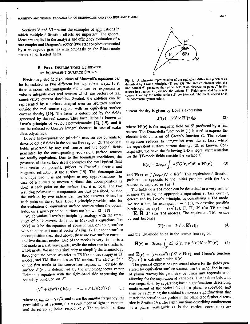
MASHKOV AND TEMK1N: PROPAGATION OF E1GENMODES ANÖ TRANSFER AMPUTUDES 2037
Sections V and VI present the examples of applications in which multiple diffraction effects are important. The general ideas are applied to the analysis and efficiency evaluation of a star coupler and Dragone's router (two star couplers connected by a waveguide grating) with emphasis on the Bloch-mode nature of diffracted fields.
II. FIELD DISTRIBUTIONS GENERATED
BY EQUIVALENT SURFACE SOURCES
Electromagnetic field solutions of Maxwell's equations can be formulated in two different but equivalent ways. First, time-harmonic electromagnetic fields can be expressed as volume integrals over real sources which are vectors of real conservative current densities. Second, the solution can be represented by a surface integral over an arbitrary surface outside the real source region, with an equivalent surface current density [19]. The latter is determined by the fields generated by the real source. This formulation is known as Love's principle of vector electrodynamics [2], [19], and it can be reduced to Green's integral theorem in case of scalar electrodynamics.
Love's field-equivalence principle uses surface currents to describe optical fields in the source-free region [21. The optical fields generated by any real source and the optical fields generated by the corresponding equivalent surface sources are totally equivalent. Due to the boundary conditions, the presence of the surface itself decouples the total optical field into vector components, subject to Fresnel's electric and magnetic refraction at the surface [19]. This decomposition is unique and it is not subject to any approximations. In case of a curved or uneven surface, this decomposition is done at each point on the surface, i.e., it is local. The two resulting polarization components are thus described, outside the surface, by two independent surface currents defined at each point on the surface. Love's principle provides rules for the evaluation of equivalent surface sources when the optical fields on a given principal surface are known [2], 118].
We formulate Love's principle by analogy with the treat- ment of bulk current densities in Maxwell's equations. Let 5'(r) = 0 be the equation of some initial, or input, surface with an outer unit normal vector n' (Fig. 1). Due to the surface decomposition described above, there are two surface currents and two distinct modes. One of the modes is very similar to a TE mode in a slab waveguide, while the other one is similar to a TM mode. We use this similarity to simplify the terminology throughout the paper: we refer to TE-like modes simply as TE modes, and TM-like modes as TM modes. The electric field of the first mode in the source-free region, i.e., outside the surface S'(r), is determined by the imhomogeneous vector Helmholtz equation with the right-hand side expressing the boundary condition on 5"
(V2 + fc2n2(r))E(r) = -iu,i03°(T)6{S'{r)) (1)
where u, /x0, fco - 2TT/A, and n are the angular frequency, the permeability of vacuum, the wavenumber of light in vacuum, and the refractive index, respectively. The equivalent surface
Fig 1 A schematic representation of the equivalent diffraction problem as described by Love's principle, (2) and (3). The surface element with the unit normal n' generates the optical field at an observation point P in the source-free region, i.e., outside the volume V. Fields generated by a real source J and by the entire surface S' are identical. The point labeled O is the coordinate system origin.
current density is given by Love's expression
Js(r) = 2n' x H'(r)|s< (2)
where H'(r) is the magnetic field on S' produced by a real source. The Dirac-delta function in (1) is used to express the electric field in terms of Green's function G. The volume integration reduces to integration over the surface, where the equivalent surface current density, (2), is known. Con- sequently, we have the following 2-D integral representation for the TE-mode fields outside the surface S'
E(r) = 2mio [ dS'G(r, r')rY x H'(i') Js"
(3)
and H(r) = (l/io>/z0)V x E(r). This equivalent diffraction problem, as opposite to the initial problem with the bulk source, is depicted in Fig. 1.
The fields of a TM mode can be described in a very similar manner by using the appropriate equivalent surface current, determined by Love's principle. In considering a TM mode, we use a bar, for example, n -> n(r), to describe possible birefringence; c(r) = 50n2(r), E, H, J" (for TE modes) —> E, H, Js (for TM modes). The equivalent TM surface current becomes
Js(r) = -2rY x E'(r)|.s< (4)
and the TM-mode fields in the source-free region
H(r) = -2iwe0 f dS'G(r, r')n2(r')n' x E'(r') (5) . JS'
and E(r) = (i/we0n2(r))V x H(r), and Green's function
G(r, r') is calculated with n(r). The general expressions presented above for the fields gen-
erated by equivalent surface sources can be simplified in case of planar waveguide geometry by using any approximation allowing for the separation of variables. This is done below in two steps: first, by separating basic eigenfunctions describing confinement of the optical field in a planar waveguide, and then by calculating the residual transverse eigenfunctions that match the actual index profile in the plane (see further discus- sion in Section IV). The eigenfunctions describing confinement in a planar waveguide (z is the vertical coordinate) are
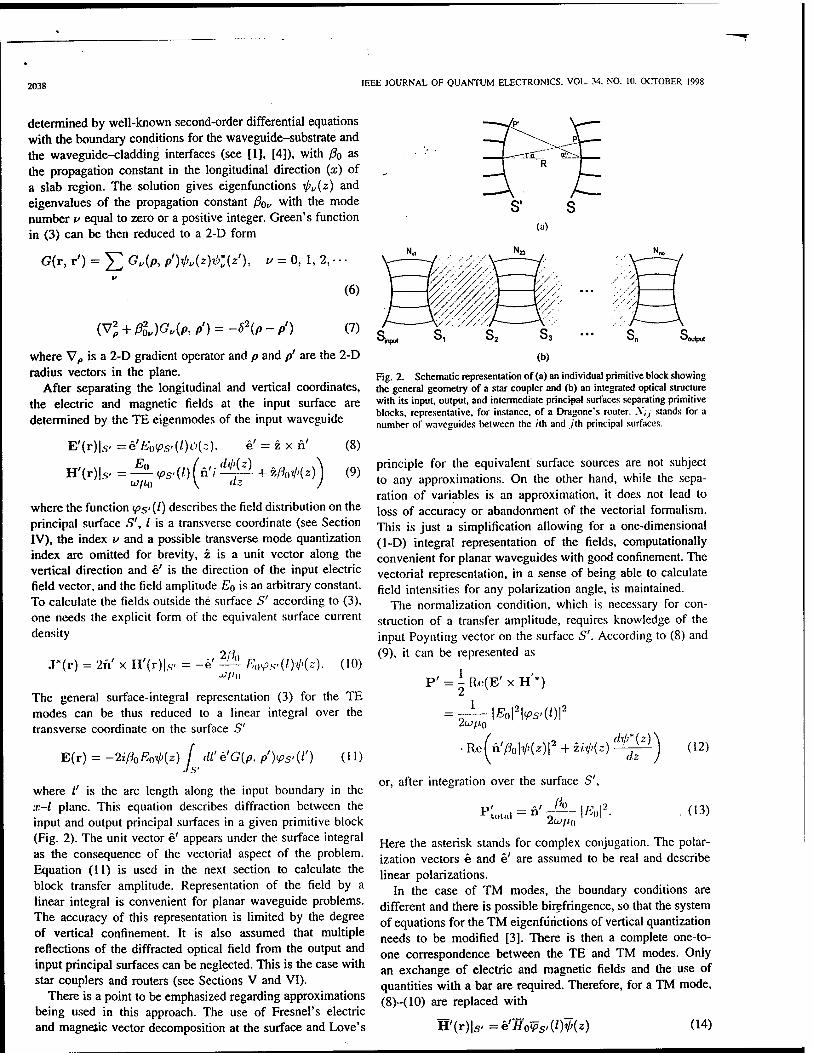
2038 IEEE JOURNAL OF QUANTUM ELECTRONICS. VOL. 34. NO. 10. OCTOBER 1998
determined by well-known second-order differential equations with the boundary conditions for the waveguide-substrate and the waveguide-cladding interfaces (see [1], [4]), with ß0 as the propagation constant in the longitudinal direction (x) of a slab region. The solution gives eigenfunctions ^v(z) and eigenvalues of the propagation constant ßo„ with the mode number v equal to zero or a positive integer. Green's function in (3) can be then reduced to a 2-D form
G(r, r') = Y, G»fa /*>,(*)#(*'). * = 0, 1, 2, ■ • ■
(v?+ /&)<?.,(* P') = -*2(P-/0
(6)
(7)
where V^ is a 2-D gradient operator and p and p' are the 2-D radius vectors in the plane.
After separating the longitudinal and vertical coordinates, the electric and magnetic fields at the input surface are determined by the TE eigenmodes of the input waveguide
E'(T)\s,=e'E0cps.(l)v(.: z x n (8)
H'(r)|.v = ^ <M0 U'i yP- + zM'iz)) (9)
where the function ips> (/) describes the field distribution on the principal surface S', I is a transverse coordinate (see Section IV), the index v and a possible transverse mode quantization index are omitted for brevity, z is a unit vector along the vertical direction and e' is the direction of the input electric field vector, and the field amplitude E0 is an arbitrary constant. To calculate the fields outside the surface S' according to (3), one needs the explicit form of the equivalent surface current density
J*(r) = 2rV x H'(r)|.s- = -e' ^i I^s-VYHz)- ■^V'o
(10)
The general surface-integral representation (3) for the TE modes can be thus reduced to a linear integral over the transverse coordinate on the surface S"
E(r) = -2iß0E„i>{z) f M'e'G{p,p')ips'{l') 0 0 ■IS'
where /' is the arc length along the input boundary in the x-l plane. This equation describes diffraction between the input and output principal surfaces in a given primitive block (Fig. 2). The unit vector e' appears under the surface integral as the consequence of the vectorial aspect of the problem. Equation (11) is used in the next section to calculate the block transfer amplitude. Representation of the field by a linear integral is convenient for planar waveguide problems. The accuracy of this representation is limited by the degree of vertical confinement. It is also assumed that multiple reflections of the diffracted optical field from the output and input principal surfaces can be neglected. This is the case with star couplers and routers (see Sections V and VI).
There is a point to be emphasized regarding approximations being used in this approach. The use of Fresnel's electric and magnetic vector decomposition at the surface and Love's
(a)
,y/////A mm. ■'input 'output
Fig. 2. Schematic representation of (a) an individual primitive block showing the general geometry of a star coupler and (b) an integrated optical structure with its input, output, and intermediate principal surfaces separating primitive blocks, representative, for instance, of a Dragone's router. .Y;j stands for a number of waveguides between the ;'th and ./'th principal surfaces.
principle for the equivalent surface sources are not subject to any approximations. On the other hand, while the sepa- ration of variables is an approximation, it does not lead to loss of accuracy or abandonment of the vectorial formalism. This is just a simplification allowing for a one-dimensional (1-D) integral representation of the fields, computationally convenient for planar waveguides with good confinement. The vectorial representation, in a sense of being able to calculate field intensities for any polarization angle, is maintained.
The normalization condition, which is necessary for con- struction of a transfer amplitude, requires knowledge of the input Poynting vector on the surface S". According to (8) and (9), it can be represented as
P' = -Ro(E'xH'*)
2tJfLQ \Eo\2\<Ps>(l)\2
■Rc(n7k|#0l2+™V'(z)
or, after integration over the surface 5',
p' - n' ^" IF I2
dij>*{z) dz
(12)
03)
Here the asterisk stands for complex conjugation. The polar- ization vectors e and e' are assumed to be real and describe linear polarizations.
In the case of TM modes, the boundary conditions are different and there is possible birefringence, so that the system of equations for the TM eigenfunctions of vertical quantization needs to be modified [3]. There is then a complete one-to- one correspondence between the TE and TM modes. Only an exchange of electric and magnetic fields and the use of quantities with a bar are required. Therefore, for a TM mode, (8)-(10) are replaced with
H'(r)|s< =S'ffo?s'(lM*) 04)

MASHKOV AND TEMKIN: PROPAGATION OF EIGENMODES AND TRANSFER AMPLITUDES 2039
E'(r)|< Ha =o7 <fS'(l) we0n
z(r)
dj,{z) „-g -r
dz
J-(r)=-2n'xE'(r)|s
2ß0
+ ZßolKz)j (15)
: —e we0n
2(r) H0Tps,m{z) (16)
These expressions for outgoing fields on the surface S are very similar to expressions for the incoming fields on the surface S' [see (8) and (9)], except for the presence of the amplitude transfer factor. Multiple reflections of the diffracted optical field from the output and input principal surfaces are neglected in (18) and (19).
The Poynting vector of the outgoing field can be easily obtained on the basis of (20) and (21)
where JiQ is the TM mode propagation constant, and the gen- eral surface-integral representation (5) for the TM modes can be reduced to a linear integral over the transverse coordinate on the surface S"
H(r) = 2iTi0H0J>(z) f dl' e'G(p, p')^>'(0- 0?) Js'
The magnetic field_amplitude ~H0 is an arbitrary constant, and Green's function G{p, p') is defined with equations similar to (6) and (7) for the case of TM modes.
There is an obvious symmetry (up to the general sign) between the propagation properties of the TE and TM modes as described by (II) and (17) for diffracted fields. In the remainder, unless otherwise indicated, we will discuss only the TE modes.
III. TRANSFER AMPLITUDES
In this section, we derive a general expression for the transfer amplitude based on (11). The field E(r) is generated in a slab region by an effective surface source on S'. It propagates from an input surface S' to an output surface 5 according to Huygens' principle and enters the system of output waveguides [see Fig. 2(a)]. Let us suppose the total eigenfunction of the output waveguide system contains a product of a new unit vector e and an eigenfunction describing vertical quantization ij){z). This representation separates the vector properties and the vertical coordinate dependence. The remaining spatial dependence, related to the transverse direction, is described by an eigenfunction tps{l) (Section IV). The electric field at the output surface is given by a product of the vertical and transverse eigenfunctions with the transfer amplitude that describes propagation and diffraction in the primitive block.
A natural way to define a dimensionless transfer amplitude for a primitive block bound by surfaces S and S" is to consider the functional and vectorial projections of the electric field E(r), as defined by (11), onto the product of eigenfunctions of the output waveguides, divided by a field amplitude EQ
t(S, S')=Y0J dS<p*s(lW(z)e • E(r) (18)
= -2ißo ! dl I dZ'e-eVs(OG(p,P>s<(0-(19) Js JS'
Orthonormality properties of the eigenfunctions tp and >p were used to get the second line in this equation. With (18), the electric and magnetic fields related to the output surface S can be represented as follows:
E(r)|s =et{S.. S')Eo<Ps(l)1>{*) (20)
P = -Rc(ExH*)
e e'\|2 2u>//.()
|£o| W)|2|'-(S, S')\
• ftc(n#> |V>(z)|2 + zii>(z[ dxl>*(z
I
dz 0 or, after integration over the surface S,
ßo , r, i2u/c c"\\2
H(r)|s=t(5,5')^^(0 (..Wz)
+ ZM(z))- (2D
Ptotal = n 2w//.o
\EQ\2\t(S, S')|J
(22)
(23)
Thus, the quantity \t(S. S')|2, where /. is defined by (18), represents a power (or intensity) transfer function for a given primitive block [Fig. 1(a)]
T(S. s') =,", ^';"al = i'(^ s')\2 iv • P:
(24) »tat
The total transfer amplitude for the entire optical system [see Fig. 2(b)] is represented by a convolution of multiple transfer amplitudes of primitive blocks, with summation over all intermediate principal surfaces
'■(■Joiit i i'in)
= Y, /('s'"" •5») • • • '-^2'5i ws>'Si»)-(25)
S^Si.-.S,,
The meaning of the sum is specified below (Section VI). The corresponding transfer function for the entire optical system is defined as
T(S0uti ^iii) — IH-Joul; Si„)| (26)
At this point, it is convenient to introduce a normalized transverse eigenfunction of the TE diffracted field, according to (19)
<p{l) = -2t/3b / dl'e - e'G(p, p')<pS'(l')- 0-1) ■IS'
It is easy to see that if the surfaces S and 5" are smooth and have low curvatures, which is the case of real integrated optical circuits, the normalization condition for the function ip{l) can be written as
[ dl\<p{l)\2 = J dl'\<ps-{l')\' 1. (28)
The concept of a normalized transverse eigenfunction of the diffracted field is very useful because: 1) the function (p(l) is defined uniquely by (27) and (28) everywhere; 2) it can be easily generalized to the case of several primitive blocks (Section VI); and 3) the transfer amplitude (19) can be
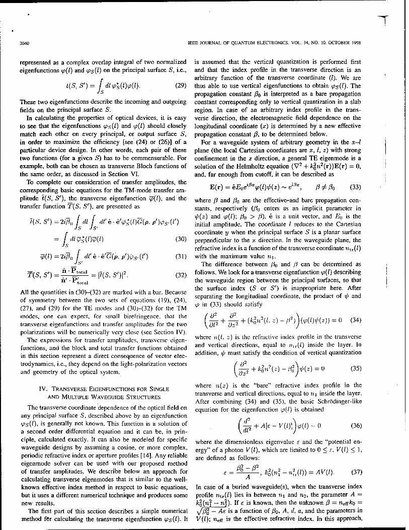
T
2040 IEEE JOURNAL OF QUANTUM ELECTRONICS. VOL. 34, NO. 10. OCTOBER 1998
represented as a complex overlap integral of two normalized eigenfunctions tp(l) and ips(l) on the principal surface S, i.e.,
t(S:S') = J dl<p*s(l)<p(l). (29)
These two eigenfunctions describe the incoming and outgoing fields on the principal surface S.
In calculating the properties of optical devices, it is easy to see that the eigenfunctions ips(l) and <p(l) should closely match each other on every principal, or output surface S, in order to maximize the efficiency [see (24) or (26)] of a particular device design. In other words, each pair of these two functions (for a given S) has to be commensurable. For example, both can be chosen as transverse Bloch functions of the same order, as discussed in Section VI.
To complete our consideration of transfer amplitudes, the corresponding basic equations for the TM-mode transfer am- plitude l.(S, S'), the transverse eigenfunction y>(l), and the transfer function T(S. S'), are presented as
7(.S\ 5') = 2ißu j d.i. j d.i.' e • eVs(0GV. p')Jps.(l'
= j' di^*(i.)W)
W) l)=2ift0 I d.i.' ee'G(p, p')ips,(l')
n • Ptotiii
n' • P: T(S, s') = ., .j;™ = \i.(s, s')f
" ' total
(30)
(31)
(32)
All the quantities in (30)-(32) are marked with a bar. Because of symmetry between the two sets of equations (19), (24), (27), and (29) for the TE modes and (30)-(32) for the TM modes, one can expect, for small birefringence, that the transverse eigenfunctions and transfer amplitudes for the two polarizations will be numerically very close (see Section IV).
The expressions for transfer amplitudes, transverse eigen- functions, and the block and total transfer functions obtained in this section represent a direct consequence of vector elec- trodynamics, i.e., they depend on the light-polarization vectors and geometry of the optical system.
IV. TRANSVERSE EIGENFUNCTIONS FOR SINGLE
AND MULTIPLE WAVEGUIDE STRUCTURES
The transverse coordinate dependence of the optical field on any principal surface S, described above by an eigenfunction ips{l), is generally not known. This function is a solution of a second order differential equation and it can be, in prin- ciple, calculated exactly. It can also be modeled for specific waveguide designs by assuming a cosine, or more complex, periodic refractive index or aperture profiles [14]. Any reliable eigenmode solver can be used with our proposed method of transfer amplitudes. We describe below an approach for calculating transverse eigenmodes that is similar to the well- known effective index method in respect to basic equations, but it uses a different numerical technique and produces some new results.
The first part of this section describes a simple numerical method for calculating the transverse eigenfunction <ps(0- I*
is assumed that the vertical quantization is performed first and that the index profile in the transverse direction is an arbitrary function of the transverse coordinate (/). We are thus able to use vertical eigenfunctions to obtain y>s(0- The propagation constant ßo is interpreted as a bare propagation constant corresponding only to vertical quantization in a slab region. In case of an arbitrary index profile in the trans- verse direction, the electromagnetic field dependence on the longitudinal coordinate (x) is determined by a new effective propagation constant ß, to be determined below.
For a waveguide system of arbitrary geometry in the x-l plane (the local Cartesian coordinates are x, I, z) with strong confinement in the z direction, a general TE eigenmode is a solution of the Helmholtz equation (V2 + £gn2(r))E(r) = 0, and, far enough from cutoff, it can be described as
E(r) = e£0e£/?X/)V'(z)
i!ix ft * flo (33)
where ß and ßo are the effective-and bare propagation con- stants, respectively (ßo enters as an implicit parameter in V'(z) and <p{!); ßo > ft)< e is a unit vector, and lia is the initial amplitude. The coordinate / reduces to the Cartesian coordinate y when the principal surface S is a planar surface perpendicular to the .-;: direction. In the waveguide plane, the refractive index is a function of the transverse coordinate ii.,r(l) with the maximum value n\.
The difference between ßa and ß can be determined as follows. We look for a transverse eigenfunction ip{l) describing the waveguide region between the principal surfaces, so that the surface index (5 or S') is inappropriate here. After separating the longitudinal coordinate, the product of rj> and ip in (33) should satisfy
W? + ipi + ^o"'2^- *) - 02))(V(OV'(2)) = 0 (34)
where ;;.(/, z) is the refractive index profile in the transverse and vertical directions, equal to »ir(') inside the layer. In addition, </> must satisfy the condition of vertical quantization
d- - + ^r(z)-ßf)U(z)=ü (35)
where n{z) is the "bare" refractive index profile in the transverse and vertical directions, equal to n.\ inside the layer. After combining (34) and (35), the basic Schrodinger-like equation for the eigenfunction tp(l) is obtained
+ A[e-V{l)\)v{l)=() (36)
where the dimensionless eigenvalue s and the "potential en- ergy" of a photon V(l), which are limited to 0 < s, V(l) < 1, are defined as follows:
£ = ßl-ß2
, *o2("i - <•(<)) = AV{1). (37)
In case of a buried waveguide(s), when the transverse index profile ntT{l) lies in between v.\ and Tt2, the parameter A = ^o(ni — n!)- If e *s known, then the unknown ß = neffk0 = \/ßo - Ae is a function of ß0, A, d, a, and the parameters in V(l)', neff is the effective refractive index. In this approach,

MASHKOV AND TEMKIN: PROPAGATION OF EIGENMODES AND TRANSFER AMPLITUDES 2041
•g- 0.20 a.
£• 0.15 «n c S c
E c o
Ul
0.10
0.05
0.00 -15
-I ■ 1 ■ 1 ■ r —■—,—,—,— -c !- . | ■
TE
" '" / \ TM .
' 1 / \ ' l
1 ' i Bloch q = n/d
' * r •J * * \ •' v./ '
y r-v// \\ «■' ,\ Bloch </ = 0
• •'' \ / v / \/ ■
I . i —^—<4_—. 1 . J=> i i ■ . i .
-10 -5 0 5 10 15
Transverse Coordinate (um)
20 25
Fig. 3. Intensities of the TE and TM eigenmodes of a single waveguide with a rectangular index profile, and two normalized Bloch functions in the periodic waveguide profile, calculated for the values of the transverse quasi-momentum q = 0 and jr/rf.
the condition of vertical quantization is included explicitly through (35).
The numerical technique based on (35) and (36) is ap- plicable with good accuracy to any index profile in the transverse direction, including profiles with abrupt boundaries in both directions and a smooth profile only in the transverse direction. The procedure of vertical quantization within the present approach is exactly the same as in the effective index method. Some examples of simultaneous evaluation of the eigenfunction tp{l) and the eigenvalue e are given below.
In the case of a symmetric slab waveguide, we start with the known transcendental equation for ß() expressed through a dimensionless variable X
tan(X) = X = ±y/(k07i1)*-(% (38)
0.5
0.4
0.3 a> 2 °-2
|- 0.1
i °° *o o -0.1 E §■ o> Li -0.3
-0.4
-0.5
• ' ! ' , x 1 -— i , i i
—- — even - . ' " :" 1 /V/V odd r j / "i"V ; ; .
:"""!/ T v \ ■
• J-. 1 ■
-.::<! 1 \ i
-
\ : i -
-- VL: 1 izi • 1 1
-15 -10 -5 0 5 10
Transverse Coordinate (urn) 15
Fig. 4. The even and odd TE eigenmodes of a symmetric double waveguide structure with strong coupling.
the consequence of tunneling through the central barrier. The tunneling is important in the analysis of optical devices such as 3-dB couplers [1].
To demonstrate the capability of our numerical method, we use (36) to evaluate the transverse eigenfunction of a periodic waveguide structure with the index profile given by V(l) = cos2(7r//r/), where d is the period. In this case, the function ip(l) is represented by a periodic Bloch function which can be expressed through standard Mathieu functions (see [20, ch. 20])
I' -ul Ad?\ qd v,(/)-,^(Z) = ce7|7..^-J, r=H- (39)
where q is the quasi-momentum in the transverse direction and v is the dimensionless index of the Mathieu function. The corresponding eigenvalue in (36) and the value of the propagation constant are determined as
' Ad2\ 1 where U = {hk0/2)>/?/.* - n\ is a characteristic parameter. This equation determines fia as a function of A, n\, n2, the layer thickness, and a quantum number of the verti- cal quantization ;/ = 0. 1. 2, •••. In the case of a single waveguide, we use (36) and (37) with the known ß0 to determine eigenvalues of the effective propagation constant ß and the corresponding eigenfunctions ip(l). The examples of the resulting eigenfunctions <p{l) for a single waveguide within a periodic structure with the refractive index difference An = 0.0085 and birefringence 0.0125 are plotted in Fig. 3. A rectangular index profile is assumed. Both the TE and TM modes are shown. The Bloch functions, also shown in Fig. 3, will be discussed below. There is a strong similarity between different eigenfunctions in Fig. 3, especially in the core wave- guide region. For example, the TE and TM eigenmodes almost coincide. Our numerical calculations have also shown that for any refractive index profile and almost everywhere in I the transverse eigenfunction is very close to a Gaussian (see also
[11])- The even and odd TE eigenmodes of a symmetric double
waveguide structure in the case of a strong coupling are plotted in Fig. 4. The presence of two eigenfunctions with different parities, and having slightly different eigenvalues, is
AiP a,. +
ß - ft, = \Jftl - Ae„ (40)
where ar(Q) is the characteristic value of the Mathieu equa- tion ce';(z, Q) + (or - 2Q cost») cer{z, Q) = 0. For the first Brillouin zone, we have 0 < |o| < n/d (0 < |r| < 1).
The normalizable part uq(l) of the Bloch function, which according to Floquet's theorem is defined by the equation <pq(l) = eiqluq(l), represents an element of the orthonormal set of functions j\i\<d/2 dluq(l)uq.(I) = V- ™s normalizable part is plotted in Fig. 3 for two values of q (0 and ir/d). Within the waveguide, all solutions are very close to each other. For q = n/d, the Bloch function behaves differently. The periodic Bloch eigenmodes obtained above cannot be, in general, excited. However, they can be excited with specific envelope functions and specific values of the quasi-momentum q (see Section V).
V. FOURIER OPTICS APPROXIMATION AND STAR COUPLERS
In this section, we consider propagation of eigenmodes and transverse eigenfunctions based on the idea of the transfer amplitude defined in (29). The general formulation discussed

2042 IEEE JOURNAL OF QUANTUM ELECTRONICS. VOL. 34. NO. 10. OCTOBER 1998
in Section III is applied here to efficiency calculations of: 1) Dragone's star coupler and 2) waveguide grating router (see Section VI).
It is well known that diffraction of guided waves in a star coupler with circular (cylindrical) principal surfaces, periodic input, and output waveguide structures, and the ratio if/ßCl (where d is the distance between waveguides in the transverse direction and R is the characteristic radius of principal surfaces bounding a slab region) can be described with high accuracy within the Fourier optics approximation [14], [21), [22]. Cal- culations of transverse eigenfunction <p(l) of the diffracted field and the transfer amplitude t.(S, S') for a star coupler in the Fourier optics approximation are considered below for different types of input and output apertures. Numerical results for the transfer function are presented as a function of the total number of waveguides and the characteristic aperture size. However, it is interesting to point out that the general method described here is applicable to non-Fourier optics situations as well.
The explicit form of the 2-D Green's function, defined by (7), for a slab region of a star coupler [see Fig. 2(a)] is given by the Hankel function of the first kind and zeroth-order (the quantization index in the propagation constant is omitted here for simplicity)
a[p,P') = -iCuk\p-p'\)
2\2irß()\p-p'\
1/2 jMp-P'\ (41)
where //,, (x) = ./(>(.'•) + /Tn(:r), and the approximation cor- responds to the asymptotic expansion of the Hankel function at H()\p — p'\ 3> 1 [2()|. The distance between points /' and /". with the angular coordinates a and M' on the arcs S and S'. respectively, is determined as \p - p'\ = //((cos n + cos iy' - I)'-' + (sin fv - sin <Y')-)
]/-', where the characteristic
values of the input and output aperture angles |M|. |n'| <C 1 [Fig. 2(a)]. Thus, in the standard diffraction approximation [191, we substitute \p - p'\ — R in the denominator and \p - p'\ — R(1 - mv') in the exponent of (41). This gives rise to the propagation function
«("■«') = 5 Ur Tfalt
1/2 ..i\V„/?(l-f»»') (42)
where we explicitly use the angular variables o and a' instead of a pair of 2-D radius vectors p and p'. It is also convenient to normalize the eigenfunctions by the angle <y instead of the arc length I = aR. [see (28)]
j dl\^>(l)\2 = J dn\<K«)\2 = 1. <p{l) = -~ 0(O).
(43) For a TE-polarized eigenmode, the product of the initial and final polarization vectors reduces to unity for |o|, |o'| <S 1 [see (19) and (27)]: e • e' = cos a cos a' - sin a sin <v' « 1. The basic equations (27) and (29) can be reformulated as
t(S,S')= [ da<Ps(a)4>(a) (44) Js
</•>(<*) = ■iftoli-
1/2
>U"n I da' .IS' 2TT
■(riß°nan'<l>s-(<y') (45)
where the integral in (45) is a typical Fourier optics integral. For diffraction problems under consideration, numerical cal- culations show that the difference between the results obtained with the approximate propagation function (42) and the exact
expression (si/4)//(, [l\s\p - p'\) is negligible. The oscillating nature of the diffracted field on the output
surface S is important. If the input into the slab region of the coupler is introduced through a single waveguide with the ordinal number in on S', the transverse eigenfunction (45) of the diffracted field on S can be represented in general by the Bloch function of the order in (in — 0, ±1. ±2. • • •):
<!>,,,((*) = <'■-'"'*"'" <M"). (46)
The exponent in (46) can be written-in the real coordinate form as ini.fi()d(y = />//, where / = <\R and // = iir^ud/R is the transverse Bloch momentum. Similar Bloch-mode excitations have been discussed by Dragone in the case of merging or tapering multiwaveguide structures 116]. The angular period of
Bloch oscillations equals 27r/(|/;/|//U'0 and is much smaller, for |m| > 1, than the characteristic spread of the diffracted field described by the function <!>»{<*). This spread, also called
the diffraction angle «V.UH-, is of the order !/r/(/V/), as determined below. On the other hand, this period is much greater than the natural angular period of the waveguiding system djR. Consequently, we obtain the following sequence
of inequalities (|;;/.| > I):
d 2 T:
".litr ,, , ~ ,-,■ H7) l»/l.»ll'' -'ll''
Diffracted waves generated by a side-waveguide input in a circular star-coupler geometry can be approximated by Bloch modes described by periodic boundary conditions. In this case, we have [see (39) and (40) and discussion of the Bloch functions in Section IV): q = 2niu/.X,d = ni.^d./R =
(ir/d.)r, N, = 2-nR/iyP ^ I», '' = mj^dn,,/- = 2m./.\, ~ 0.2m, and |?»| < 5 for the first Brillouin zone. The periodic
boundary is applied at a distance N,d. It should be emphasized that in the overlap integral in /.
[see (44)], Bloch oscillations in </>(n) cannot be compensated by a choice of the appropriate value of d/R because in is a variable (■;//. = 0. ± I. ±2. • • •). For the central waveguide input, the Bloch factor equals I (m = 0). The field produced on the output surface 5 by each side-waveguide input (in £ 0) is harmonic [see (46)]. This field enters the output waveguide structure and propagates through it, conserving the specific phase relationship (for the transverse Bloch functions) between different waveguides (see Section VI). Consequently, to pro- vide the highest overlap of the transfer amplitude [see (44)], the eigenfunction at the output </>s(«). determined on 5, should contain a Bloch function factor (e-''»"V<>) as well, with the
same value of rn as in <j>(a) [see (45) and (46)]. For a single-waveguide input with a transverse rectangular
aperture 2a, the nonperiodic part <f>0 of the eigenfunction is

MASHKOV AND TEMKIN: PROPAGATION OF EIGENMODES AND TRANSFER AMPLITUDES 2043
10 "c S S 8
<0
5 2
0 -0.4
I ■ I I '— 1 1 1
rectangular - cosine Gaussian • A
/i\....:— / I I
//1M
. h\ ■
' 1 \ i V ■ 1)
1 -Vjl-- -' i- — _. —
1.0
-0.2 0.0 0.2
Angular Coordinate (radian)
0.4
Rg. 5. Intensities of the nonperiodic parts <M") of transverse eigenfunc- tions as determined from (48) (2« = G /rai) and (49) (d = 10 /im). The output intensity generated by a Gaussian input eigenmode, as an approximation to the TE and TM eigenmodes in Fig. 3, is also shown.
given by (45) as 1/2
eißRsmc(ßaa) (48)
where sinc(:r) = sin(a;)/a:. There are two special cases of a = d/2, which corresponds to the case of waveguides merging at S', and a = d,/4, which corresponds to a periodic step-index waveguide structure on S'.
For a single waveguide input with a periodic cos2(wRa/d) aperture profile, the nonperiodic part 4>Q of the eigenfunction is given by
1/2 ™-m eiftR 1
m sine
1 - m
0.8 -
0.0
-i 1 ■ 1 ■ r
■a = oV2, merging • a = d/4, merging
—cosine
5 10 15 20
Number of output waveguides
25
Fig. 6. Efficiency T(S, S') of a star coupler plotted as a function of the number N of output waveguides in the case of a single-waveguide input. We show two cases of a waveguide system merging on 5 with a = d/2 and a = d/4 [(48), solid and dashed lines, respectively], and a case of a periodic cos2(*Ra/d) aperture profile on 5 [(49), dashed-dotted line].
(49) The first zero of this function occurs at a = «,*;// = 4ir/ßod. The resulting angular distributions of </->o(oO along with the distribution generated by a Gaussian input eigenmode are depicted in Fig. 5.
When the eigenfunctions <j>a{n) and </>s(«) are known, the integral in (44) can be easily evaluated. The calculated transfer functions T = \t\2 are presented in Fig. 6 for different values of N. Transfer functions are sensitive to the size, the total number, and the periodicity of the input and output waveguides. This allows for easy optimization of the device. The calculated values for the star coupler's efficiency are realistic and relatively high, reaching a maximum of ~80%. This efficiency is obtained with the condition of zero aperture outside the waveguide, as used previously by Dragone [14].
VI. SIMULATION OF A WAVEGUIDE GRATING ROUTER
Having calculated the diffracted field distribution in a star coupler, we now turn to a more complicated optical system of two star couplers connected by a multiwaveguide struc- ture, a version of Dragone's router [15], [23] (Fig. 7). The discussion of a waveguide grating router consists of three parts. We first discuss a connection between the convolution of transfer amplitudes and Bloch modes. A zero waveguide-width approximation is then used to obtain relationships between
Fig. 7. An optical system consisting of two star couplers connected by the multiwaveguide structure, known as the Dragone's router.
various waveguide parameters of the router. In the third part, we calculate the optical response function of the router and present results of numerical simulations.
In the router illustrated in Fig. 7, there are four principal surfaces: the input surface 5in with the angular variable a', the two intermediate surfaces Si and S[ (variables «i and a[, respectively), and the output surface 5out with the variable a. For this system of surfaces, the direct application of (25) results in the following specific form:
t(So„t, Sin) = £ *(Sout, S[)t(S[, SMSu Sin) (50)
where t{Su S-m) and t(Sout, Si) are the transfer amplitudes for the two star couplers, i.e., the two slab regions; and t(S[, Si) is the transfer amplitude for the waveguide grating. However, as written, this is only a formal relation and the meaning of summations over principal surfaces is not defined.
It is convenient to use equations similar to (27) and (29) [or (44) and (45) for the angular variables] to express the total transfer amplitude t(SouU S\n) in terms of diffracted fields in Dragone's router. From the purely geometrical consideration, one can establish that the transmission through the multi-

204-4 IEEE JOURNAL OF QUANTUM ELECTRONICS. VOL. 34. NO. 10. OCTOBER 1998
waveguide grating, from Si to S[ [represented formally by /.(SJ, Si) in (50)], can be described by a specific transfer amplitude, called here W(a\, «i), which is related to the grating geometry and the detailed shape of the waveguide openings at the two surfaces. When both star couplers are of the same shape and size, the transfer amplitude W is proportional to the delta function of its arguments, and we
get the following symmetric form:
W(«i, «i) = «;(«,)«(*>'i -"i) <5')
where the single-parameter phase factor ir(<\ i) describes phase shifts between adjacent waveguides arising from their relative
displacements and different optical paths between Si and S[. Since the radiation and absorption losses are assumed to be negligible, the absolute value of the phase factor is taken as 1. For the two star couplers of different sizes, a scaling factor
should be introduced in (51). The Dirac-delta function in (51) is very important since it
can be easily expanded into complex Fourier series |24|
*K -«I)=AI'W(/V(«'I -'h)) = fad A (_
•l-K ^
,./!'. -< (52)
where it is easy to recognize the Bloch exponentials similar to that defined in (46). The product fa <l is simply a normalization factor. As a result, the waveguide transfer amplitude can be decomposed in terms of a complete orthogonal set of basic
Bloch modes. Consequently, if we interpret the summation in (50) as
integration over the angular coordinates on each principal
surface, that equation can be reformulated as
/(S,„„. Sin)= Y, '■».(■s'.."-)/.»('S'i») (53)
or, after introducing the integral kernel A',
(f>{a) = / dn'K(a, a')4>Siu(n') (56) •/Si,,
K(a,a')=(-2iß0R)2 f daiG(a, m)w{al)G[n1. «')• Js,
(57)
The remaining double integral in (56) and (57) is quite simple in the Fourier optics approximation. Let's consider a zero-width approximation in which the grating produces a periodic signal on the output surface S,„„. The charac- teristic function to in (55) can be represented by a sum of discrete contributions from each waveguide in the grating; each contribution is included with a phase factor describing
the corresponding optical path
which means that the Bloch function with a specific number •;;/ propagates through the waveguide «rating without distortion.
Partial transfer amplitudes, for each Bloch index in, are determined by substituting the formal summation over St or S[ with integration over cv L or «',. This representation, with partial transfer amplitudes for each index m, (53), contains only double diffraction in the two star couplers. The Bloch- mode transmission through the grating is only implied. While in this shortened description there is no explicit summation over surfaces S, and S[, this picture is still equivalent to the
initial (50). Once the summation procedure over principal surfaces is
specified, (50) can be reduced to the integral form (44). Using (51), the general formulas describing double diffraction in two
star couplers can be represented as
/(S,,,,,., S:,,) = / A«<As.„»0(«) <54> ■Is
<fr{a)=-2iß0R [ da[G(a,a\) dai«.'(<vi) ■Is] h,
x S{n\ - «,) (-2iß{)R) / da' G(au a') ■I s,„
•&*„(«') (55)
w(cti) = a,i ]P v.""iS}i((Y\ - .so,/) (58)
where A is the length difference between adjacent waveguides connecting Si and S\, the product of (iA is the corre- sponding optical path difference between waveguides, and .s- = 0. ±1. ±2, •••. The factor n,; was chosen here for convenience. By using (42) for G'(o. o') and performing the integration over infinite limits, we get an analytical expression
K{n, n) = -ifaRi •>m„n (X'i ,x<l Y^ r/-s(riA-;t,./(-.+.i +1« ))
2TT (59)
The complex Fourier series can be expressed in terms of a periodic delta function using the well-known formula related
to Floquet's theorem
52 r.-''"« = 2n Y, 'M£ + 2*/') (60)
Equation where £ is a variable and .s, /> = 0. ± 1. ±'2. (59) is then represented as
*(„„■) =-.,«« £ s(„+,.-|^ + g). />= — DO V
(61)
The grating thus generates a periodic delta function in the transfer amplitude. The argument of the delta function means that the output field in (56) is a set of shifted and inverted images of the input field. In practice, the integration is per- formed over a finite region and a smooth bell-shaped function substitutes for each delta function in (61).
Equations (56) and (61) have important applications to wavelength multiplexing and demultiplexing in integrated op- tical circuits. Suppose the input to the router consists of four closely spaced and equidistant wavelengths in a single waveguide, with four corresponding values of propagation constants ß and ß0. This set of wavelengths can be represented
by
(62)
(63)
A„ =A0(1 + ne)
ft„ =0(1-ne), ßo„ =ßa(l-ne)
where n - 0, 1,2, 3, and A0, ß, and ß0 are the initial values for the (de)multiplexing problem. These expressions for ß and

MASHKOV AND TEMKIN: PROPAGATION OF EIGENMODES AND TRANSFER AMPLITUDES 2(M5
ßo are valid for e < 1. To resolve two adjacent wavelengths, the following condition on the last term in the argument of the delta function in (61) must be satisfied:
2-KJH) 2TTJ)O 2-KVtt ^
l\).„+id (h„d Pod £ = rtrf (64)
where ;>o is the order of the diffraction maximum. This condition includes contributions from propagation constants of different wavelengths. Higher order maxima are present, with the same intensity, due to the periodicity of the delta function in (61). Thus, if the parameter p0 is chosen in such a way as to make (64) equal to the angular period atl of the waveguide structure, then the «' in the delta function in (61) takes the following values:
a = —a iuy.,1 + n,i (65)
where n = 0. 1. 2. 3. The light of any wavelength can be thus directed to any output waveguide, depending only on the input waveguide used and the parameter A. The phase shift a,i/e in the argument of (65) can be partly or entirely compensated for by choosing the value of the characteristic path difference A. For example, complete compensation is achieved for
A = — — d. /I c
(66)
The light of wavelength A0 entering the central input wave- guide is thus directed to the central output waveguide. The same light entering the waveguide m is directed to the output waveguide -/;/.. The light of wavelength Ai is displaced by one angular period of the grating, etc.
The different wavelength contributions are totally separated (demultiplexed) in space (angular) variable and
O(n) y^ ^,,'A.s-,,, (-'>: - na,i (67)
the efficiency of a router: the efficiency calculated in this way is always underestimated. However, (64) and (66) represent a general relationship between waveguide parameters and are in fact approximation-independent.
To simulate a real router with a finite waveguide width, we use the idea of universality of diffracted eigenmodes in star couplers. For identical star couplers, the nonperiodic parts of diffracted eigenmodes, (/)()(n), generated by single opening apertures are exactly the same, see (46). This has two direct consequences. First, the diffracted wave in the first star coupler gives rise to the interception factor fK in the optical response function of a router. The factor /„. is defined for each input wavelength and each waveguide in the grating as
/ ;= / |0o(«)|2'^ \./Ml ,,—»1(1
(68)
where a„ = a/H and « = 0. ±1, ±2, • • •. The factor fs is a smooth function of s because the angular width of each waveguide r>,/ is much smaller than the diffraction angle <*,nir in (47). The interception factor is a measure of the efficiency of a single star coupler
where <•.,, is the amplitude coefficient of a contribution with A„ in the input signal. We conclude that the input signal is totally demultiplexed on the output surface of Dragone's router, i.e., each wavelength enters its own output waveguide. When the phase shift in (65) is not completely compensated for, an additional phase shift should be entered into (67). This might be useful when it is desirable to send any wavelength to any particular output waveguide.
It is easy to estimate the angular dimension of the grating by using real values for the initial wavelengths and the channel separation: for instance, A() = 1.552 52 //in and AA = 0.0032 //m. respectively. In this case, e = AA/A() = 2.06 x H)-3. This corresponds to the diffraction maximum of the order /,„ = A) d.n,,/2irc = 10G in (67). By making the optical path differences A equal to tpdi, where di is the spatial period of waveguides in the grating, and compensating for the phase difference of (66), we obtain <p = ndd/edi. For <7, = 100 //m. ten times larger than the waveguide period d at the principal surface, we calculate ip = 27.75°.
Equations (64) and (66) were obtained in the zero-width approximation. This approximation cannot be used to calculate
(69)
(see also the last paragraph of Section V). By varying the waveguide width (2«) and the total number of the output waveguides (Ar) of the star coupler, the efficiency can be optimized (see Fig. 6).
Second, according to (46), the nonperiodic diffracted ampli- tudes </>„(<■ i) produced by each input opening in the second star coupler are also identical. Thus the router response function itself is proportional to </>()(a). Collecting these ideas together, we can construct the following expression for the normalized amplitude response function of a router with a finite waveguide width:
O('t) = Oii(n) £'. ..,.s(,iJi- ..*„,/(,. +1,1.1.,)) (70)
where the summation over .s is carried out for all waveguides in the grating and in is the ordinal number of the input waveguide of the router. According to (64) and (66), the combination f1A in the exponent equals 2np0 where the order of the diffraction maximum ]>o is integer.
An example of wavelength demultiplexing based on (70) is shown in Fig. 8 which plots the diffracted intensities for four wavelengths as a function of the output angle. Numerical results for wavelength multiplexing produced in the central channel by the two adjacent waveguide inputs with two different wavelengths are illustrated in Fig. 9 for the total number of waveguides in the grating TV .:= 29 and 2a = 6 //.m.
A simple estimate can be given to show the kind of effi- ciencies expected from this description of a router. Assuming a rectangular shape of the input eigenmode (fis-,,, («')> we make use of the sine-function representation [see (48)] and approxi- mate the interception factor by using the mean-value theorem for the integral |see (68)] /„ ~ y/nd\^)n(.iaa)\. A rough estimate of (70) can be obtained by changing the summation

2046 IEEE JOURNAL OF QUANTUM ELECTRONICS, VOL. 34, NO. 10. OCTOBER 1998
160
140
£ 120 •o co *100
f80
| 60
& 40
O 20
0 -0
1 1 1 r
X0=1.55252 urn f
■ x
—i 1 1 1 1
X =1.55572 um
—, , ,
1.55892 um
: M I ." -31=1.56212 um.
: U \\/ -
Ü, I , I
■•" i
■
02 -0.01 0.00 0.01 0.02 0.03 0.04 0.05
Angular Coordinate (radian)
Fig. 8. The output intensity of a router as a function of the angular coordinate; wavelength demultiplexing produced by a multiwavelength input at the central waveguide.
CO
g-20
= -30
Xa- 1.55252 urn 0.0032 urn
-40 1.546 1.548 1.550 1.552 1.554 1.556 1.558 1.560 1.562
Wavelength (urn)
Fig. 9. An example of wavelength multiplexing: inputs into two adjacent waveguides result in the output at the central waveguide. The output intensity (on a decibel scale) is plotted as a function of wavelength. The input wavelengths are An into the central waveguide and A» + AA into the first adjacent side waveguide.
to integration over ,s and using the Fourier transform of a sine function (ff^ e^sinoO-i;) da = TT 6(1 -/r), where 0(.r) is the step function). The result can be represented as
<p{a) ~ <M«) Aira
Ihd2
1/2
^Si„(-«-maj). (71)
In this approximation, the output signal is also rectangular with the width equal to 2a. Because of the strong inequality fv,j -C «.uff. the peak height is proportional to <l>0(—m(\>,i), i.e., it slowly decreases with |m|. The maximum intercept is provided in the case of waveguides merging on the output surface of the first star coupler [a = d/2, see (69)]. Using the normalization condition for the eigenmode <£sin, the estimated integrated peak intensity of the output signal (71) is given by
/ \4>{a)\2da —-\<j)o(-mad)\2.
Pod (72)
According to (48), |0o(O)|2 is proportional to a. In the case of a central input and output (ra = 0), we get the following numerical values of the router efficiency: 60% for a = 3 fim and 80% for a = 4 /xmi, both for d = 10 jtm.
In reality, the shape of the input eigenmode <j)S]u {a') and the router amplitude response function </>(a) are not rectangular and there are no analytical expressions for <f>(a). Numerical calculations show, however, that we can still use an expression for the response function similar to that given by (71). In general, the effect of demultiplexing is described by
3
<f>(a) ~ 4>0{-mad)Q ^ cnt/>(W(-a - (m + n)ad) (73) n=0
with the obvious features of (67) and (71). Here Q is the numerical factor which reduces to the square-root factor in (71) in the rectangular approximation, and <j>dd{a) is the exact double-diffracted transverse eigenmode on the output surface of the router. The router efficiency can be obtained by integration of \4>dd\2 over the angular aperture of a given output waveguide. In this way, we can get the following numerical values of the router efficiency: 54% for a = 3 //.m and 72% for « = 4 /im which are in reasonable agreement with the results of the rectangular approximation (2a here is the waveguide width).
The resolving capability of the device depends on the total number of waveguides in the grating section. On the other hand, the total efficiency is determined by the waveguide width. Fig. 10(a) and (b) shows two examples of optimization of a waveguide grating router, one for 'la = 6 //m and the efficiency 54% and another for 2« = 8 /tm and the efficiency 72%, as a function of N. The principal maxima in both figures change only slightly while the first sidelobes decrease dramatically with increasing N. In the case of Ar = 29 and 2« = 8 //.m [Fig. 10(b)l, the difference between the principal maximum and the first sidelobe exceeding 30 dB is demonstrated in this simulation.
VII. SUMMARY
We present a method of modeling and simulating inte- grated optical circuits. It is based on the vector-electrodynamic formulation of field distributions and transfer amplitudes in optical waveguides, and it is equivalent to Huygens' picture of propagation and diffraction of time-harmonic electromagnetic fields. Thus, it has a clear physical background. The method consists of the following steps:
1) dividing a waveguide system into a set of primitive blocks separated by principal optical surfaces, and de- termining boundary values of electromagnetic fields and their polarization;
2) expressing the diffracted fields through surface inte- grals, generated according to Love's field equivalence principle, by the equivalent surface current densities;
3) computing the transfer amplitude for each block sepa- rately, and accounting accurately for effects of diffrac- tion;
4) calculating the transfer amplitude of the entire optical system as a convolution integral of transfer amplitudes of its primitive blocks;
5) evaluating the total transfer amplitude, as a function of physical characteristics of a device, such as the size and
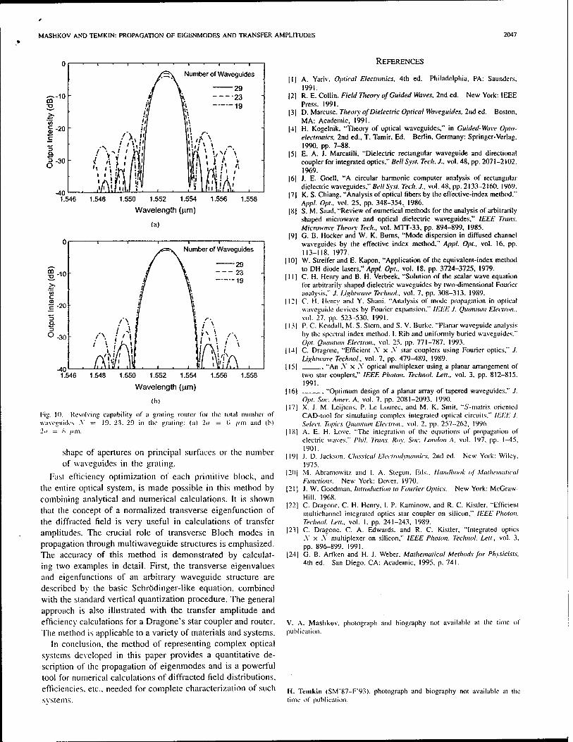
MASHKOV AND TEMKIN: PROPAGATION OF EIGENMODES AND TRANSFER AMPLITUDES 2047
1.546 1.548 1.550 1.552 1.554 1.556 1.558
Wavelength (urn)
(a)
1.546 1.548 1.550 1.552 1.554 1.556 1.558
Wavelength (p.m)
(b)
Fig. I0. Resolving capability of a grating router for the total number of waveguides .V = 19. 23. 20 in the grating: (a) 'la = G pm and (b) J.i — S /i m.
shape of apertures on principal surfaces or the number of waveguides in the grating.
Fast efficiency optimization of each primitive block, and the entire optical system, is made possible in this method by combining analytical and numerical calculations. It is shown that the concept of a normalized transverse eigenfunction of the diffracted field is very useful in calculations of transfer amplitudes. The crucial role of transverse Bloch modes in propagation through multiwaveguide structures is emphasized. The accuracy of this method is demonstrated by calculat- ing two examples in detail. First, the transverse eigenvalues and eigenfunctions of an arbitrary waveguide structure are described by the basic Schrödinger-like equation, combined with the standard vertical quantization procedure. The general approach is also illustrated with the transfer amplitude and efficiency calculations for a Dragone's star coupler and router. The method is applicable to a variety of materials and systems.
In conclusion, the method of representing complex optical systems developed in this paper provides a quantitative de- scription of the propagation of eigenmodes and is a powerful tool for numerical calculations of diffracted field distributions, efficiencies, etc.. needed for complete characterization of such systems.
REFERENCES
[1] A. Yariv. Optical Electronics, 4th ed. Philadelphia, PA: Saunders, 1991.
|2) R. E. Collin. Field Theory of Guided Waves, 2nd ed. New York: IEEE Press, 1991.
|3] D. Marcuse. Theory of Dielectric Optical Waveguides, 2nd ed. Boston, MA: Academic, 1991.
14] H. Kogelnik. "Theory of optical waveguides," in Guided-Wuve Opto- electronics. 2nd ed., T. Tamir. Ed. Berlin, Germany: Springer-Verlag. 1990. pp. 7-88.
|5| E. A. J. Marcatili, "Dielectric rectangular waveguide and directional coupler for integrated optics," Bell Syst. Tech. J., vol. 48, pp. 2071-2102. 1969.
|6| J. E. Goell. "A circular harmonic computer analysis of rectangular dielectric waveguides," Bell Syst. Tech. J.. vol. 48, pp. 2133-2160, 1969.
|7| K. S. Chiang, "Analysis of optical libers by the effective-index method." Appl. Opt., vol. 25. pp. 348-354, 1986.
(8] S. M. Saad. "Review of numerical methods for the analysis of arbitrarily shaped microwave and optical dielectric waveguides," IEEE Trans. Microwave Theory Tech., vol. MTT-33, pp. 894-899, 1985.
|9] G. B. Hocker and W. K. Burns, "Mode dispersion in diffused channel waveguides by the effective index method." Appl. Opt., vol. 16, pp. 113-118. 1977.
110] W. Streifer and E. Kapon, "Application of the equivalent-index method to DH diode lasers," Appl. Opt., vol. 18. pp. 3724-3725, 1979.
1111 C. H. Henry and B. H. Verbeek, "Solution of the scalar wave equation for arbitrarily shaped dielectric waveguides by two-dimensional Fourier analysis." J~Lightwave Teclmol. vol. 7. pp. 308-313. 1989.
|12| C. H. Henry and Y. Shani. "Analysis of mode propagation in optical waveguide devices by Fourier expansion." IEEE J. Quantum Electron.. vol. 27. pp. 523-530. 1991.
113| P. C. Kendall. M. S. Stem, and S. V. Burke. "Planar waveguide analysis by the spectral index method. I. Rib and uniformly buried waveguides." Opt. Quantum Electron., vol. 25. pp. 771-787, 1993.
|I4| C. Dragone, "Efficient .Y x .Y star couplers using Fourier optics." J. Lightwave Techno!., vol. 7, pp. 479^*89, 1989.
[151 . "An -^ x -^ optical multiplexer using a planar arrangement of two star couplers," IEEE Photon. Teclmol. Lett., vol. 3, pp. 812-815. 1991.
116] "Optimum design of a planar array of tapered waveguides." / Opt. Soc. Amer. A. vol. 7. pp. 2081-2093! 1990.
|I7| X. J. M. Leijlens. P. Lc Lourec, and M. K. Sniit. "S'-niatiix oriented CAD-tool for simulating complex integrated optical circuits." IEEE J. Select. Topics Quantum Electron., vol. 2. pp. 257-262, 1996.
| IS] A. E. H. Love. "The integration of the equations of propagation of electric waves." Phil. 7'ra/i.v. Row Soc. London A. vol. 197. pp. 1-45. 1901.
119| J. D. Jackson. Classical Electrodynamics. 2nd cd. New York: Wiley. 1975.
|20] M. Abramowitz and 1. A. Stegun. Eds.. Handbook of Mathematical Functions. New York: Dover. 1970.
|2I ] J. W. Goodman. Introduction to Fourier Optics. New York: McGraw- Hill. 1968.
|22| C. Dragone. C. H. Henry. 1. P. Kaminow. and R. C. Kisller. "Efficient multichannel integrated optics star coupler on silicon," IEEE Photon. Teclmol. Lett., vol. I, pp. 241-243, 1989.
|23] C. Dragone. C. A. Edwards, and R. C. Kisller, "Integrated optics .Y x -Y multiplexer on silicon," IEEE Photon. Teclmol. Lett., vol. 3, pp. 896-899. 1991.
|24] G. B. Arfken and H. J. Weber, Mathematical Methods for Physicists, 4th ed. San Diego. CA: Academic, 1995, p. 741.
V. A. Mashkov. photograph and biography not available at the time of publication.
H. Temkin (SM'87-F*93). photograph and biography not available at the time of publication.

JOURNAL OF APPLIED PHYSICS VOLUME 83, NUMBER 4 15 FEBRUARY 1998
Low-frequency noise and performance of GaN p-n junction photodetectors D. V. Kuksenkov^ and H. Temkin Electrical Engineering Department, Texas Tech University, Lubbock, Texas 79409
A. Osinsky, R. Gaska, and M. A. Khanb)
APA Optics, Inc., 2950 N.E. 84th Lane, Blaine, Minnesota 55449
(Received 8 September 1997; accepted for publication 6 November 1997)
We report on low-frequency noise characteristics of visible-blind GaN p-n junction photodetectors. Carrier hopping through defect states in the space charge region, believed to be associated with dislocations, is identified as the main mechanism responsible for the dark conductivity of the photodiodes. Under reverse bias, the dark current noise has the 1// character and obeys the Hooge relation with a~3. Under forward bias, we observe generation-recombination noise related to a trap level with the activation energy of 0.49 eV. Under illumination, detectivity is found to be shot noise limited. The noise equivalent power of a 200X200/tm2 photodetector is estimated at 6.6 X10"l5 W/Hz1/2 at a bias of - 3 V. © 1998 American Institute of Physics. [S0021-8979(98)05504-2]
ajasai'
I. INTRODUCTION
Ultraviolet-sensitive photodetectors with a sharp cutoff for the visible spectral range have a number of applications in spectroscopy, flame sensing, etc. Due to the large direct band gap, gallium nitride is ideally suitable for the prepara- tion of such photodetectors. Significant progress has already been achieved in the development of Schottky barrier GaN- based detectors,1,2 resulting in responsivities as high as 0.18 AAV and a bandwidth in excess of 10 MHz. However, the performance of Schottky diodes is typically limited by rela- tively large leakage currents. The reverse bias leakage cur- rent in a p-n junction diode is expected to be significantly lower than in a Schottky barrier diode due to the larger bar- rier height This promises a corresponding performance advantage.3,4 Indeed, p-n junction based GaN photodiodes with dark currents as low as a few pA have been demon- strated recently.5
Characterization of low-frequency noise is needed to as- certain performance of photodetectors. Noise measurements provide a valuable diagnostic tool for the evaluation of elec- tronic and optoelectronic devices and their long term performance.6 In the case of photodetectors, the detectivity is limited by the level of internal noise, usually expressed as the noise equivalent power (NEP). In this work, we use low- frequency noise measurements of GaN-based p-n junction detectors to analyze mechanisms of dark conductivity and device performance.
II. SAMPLE PREPARATION
Devices investigated here are grown on sapphire sub- strates by metalorganic chemical vapor deposition (MOCVD). The details of device design and fabrication pro- cedures are given elsewhere.5 The photodiode structure con-
"'Electronic mail: [email protected] b)Current address: Department of Electrical and Computer Engineering, Uni-
versity of South Carolina, Columbia, SC 29208.
sists of a thin A1N buffer layer, followed by a 0.8 fim thick n-type layer of GaN (doped n—1018 cm-3) and a 2.2 yum thick p-type layer of GaN doped with Mg. The p-doping level varies along the growth direction from ~ 1016 cm" at the p-n junction interface to «7X 1017 cm-3 at the contact surface. This results in a.p-ir-n structure, where ^stands for a lightly doped compensated p-type layer sandwiched be- tween more heavily doped p and n layers. The doping levels are determined from capacitance-voltage (C-V) and Hall measurements. Reactive ion etching is used to define rectan- gular mesas of individual diodes prior to Ohmic contacts deposition.
The photodiodes responsivity reaches 0.14 AAV at 363 nm, and it drops by more than three orders of magnitude above the cutoff wavelength. From -2 to -20 V the pho- tocurrent is almost independent of the reverse bias. The pho- todiode bandwidth of «32 MHz is determined from the mea- sured detector response to ~ 1 ns long laser pulse.
III. DARK CURRENT MEASUREMENTS
Reverse bias current-voltage (/-V) characteristics of GaN photodiodes are measured in the temperature range from 290 to 570 K. Figure 1 presents five of the curves, taken on a 200X200 /im2 device. All of the curves show an exponential increase in the dark current with bias voltage. An increase in the dark current with the device temperature, for a given value of the reverse bias, is also approximately exponential.
The exponential dependence of the dark current on both the voltage and temperature is difficult to explain by conven- tional models for reverse-bias conductivity.7 Measurements of devices with different sizes show that the current scales with the device area, rather than the perimeter of the active region, thus ruling out any significant contribution of leakage currents at the device mesa sidewalls. Due to the large band gap of GaN and extremely small thermal excitation rate, dif- fusion currents in the neutral region and generation-
0021 -8979/98/83(4)/2142/5/$15.00 2142 6 1998 American Institute of Physics

J. Appl. Phys., Vol. 83, No. 4, 15 February 1998 Kuksenkov et al. 2143
nifm
1 ■ ■ ■ ■ 1
■
•n1' ' ■
*^V"\ \ S48K
\ \ \ 488K
\ \ 418K •
f ' / f1/ \ 353 K 1
'■ I / / 298 K ■
/ • '■■■■ l-...^-
-
10"
10-«
io-7
^10"* <
I io- 10"
1Ö*
10" 0 5 10 15 20 25 30 35
Reverse bias (V)
FIG. 1. Reverse bias branch of the current-voltage characteristics for a 200X200/im2 photodiode at five different temperatures. Fitting results are shown by dashed lines for the low-bias data and by dotted lines for the high-bias data.
recombination (g-r) currents in the depletion region should be negligibly small. Even though the room temperature dark current for low reverse bias is less than 1 pA, that is still 106
times higher than the saturation current of ~2X 10"l8 A ex- pected from the thermal excitation of carriers. The onset of impact ionization in the photodiodes under test is observed only at a bias of approximately -42 V, and therefore it is not expected to contribute significantly to the measured low voltage /- V characteristics. Finally, direct band-to-band or trap assisted tunneling currents have exponential voltage de- pendence, but should be only weakly temperature dependent
The conductivity of GaN diodes can be modeled by as- suming that the current is due to hopping of charged carriers via localized defect-related states (traps) in the depletion re- gion. Hopping was studied extensively in amorphous semi- conductors, where it was found to be the dominant mecha- nism of current flow, especially at low temperatures.8 Hill9
and Pollak and Riess10 concluded, using different arguments, that for moderate electric fields, the current-field dependence is described by:
y=y(0)exp eFa IT0
2kT\ T
1/4
(1)
where j is the current density, j(Q) is the low-field current density, T0 is a characteristic temperature parameter, T is the temperature, it is the Boltzmann constant, F is the electric field, e is the electron charge, C is a constant of the order of unity, and a is the localization radius of the electron wave function. At very low fields hopping conductivity cr(F) =j{F)IF is expected to follow Mott's law for variable-range hopping:"
1/41
<T(0)<X exp (2)
where T0 is the same parameter as in Eq. (1). The validity of Eq. (2) was experimentally demonstrated for many amor- phous solids.12,13
We use Eq. (1) to fit the experimental 1-V data for reverse bias ranging from — 1 to —6 V. We assume that, for this bias range, the total current through the p-n junction is equal to the saturation current originating in the depletion region and its density is given by Eq. (1). The depletion region width w was extracted from the measured capacitance-voltage (C-V) characteristics. The average electric field dependence on the reverse bias V was then found from F=(V+ V,)/w, where V, is the built-in junction voltage (estimated at ~ 1 V). Using this relation, we convert the measured current-voltage data into a current-field depen- dence, at each temperature, which can be fit directly with
Eq. (1). The best fit to the experimental data for all temperatures
is shown in Fig. 1 by dashed lines. At each temperature, two fitting parameters are used: zero-field current density j(0), and r=Ca(T0/T)m, which has a physical meaning of the characteristic jump length. The temperature dependence of y(0), fitted with Eq. (2), is used to extract the parameter T0
of 1.16X10,0K. This value of T0 is approximately three orders of magnitude higher than the JT0««10
7 usually ob-
served in amorphous semiconductors such as germanium, silicon, or heavily implanted GaAs.14 The high value of T0
explains the strong temperature dependence of the reverse- bias current in our photodiodes. Assuming a localization ra- dius of a -10 A,,s for a known T0, we obtain C=0.4 from the temperature dependence of the parameter r, a median value between C=0.8 obtained by Hill9 and C=0.17 ob- tained by Pollak and Riess.10 Finally, the density of states, per unit energy, taking part in hopping conduction is esti- mated from Af~18/(Moa3),16 as - 1.8X 1016 cm-3 eV_1.
It is surprising to find in a crystalline semiconductor the type of conductivity previously observed in amorphous sol- ids or at very low temperatures. We believe that the reason for this is high dislocation density in epitaxial GaN. For a typical dislocation density of 108 cm-2, there are on average 40 000 dislocations in a 200X 200 /im2 device. The dangling bonds at dislocation boundaries are likely candidates for the equivalent of localized states taking part in hopping conduction.17
Equation (1) is expected to be valid only for fields F <€(2kT/ea)°°*5Xltf V/cm, at room temperature. It is evi- dent from Fig. 1 that the slope of measured l-V character- istics changes noticeably for reverse bias voltages higher than ~7 V, which corresponds to the electric field of —2.2 X10⁵ V/cm We believe that at higher bias the diode con- ductivity behavior can be explained by a combination of hopping and Poole-Frenkel effect, or field-assisted thermal ionization of carriers from traps in the depletion region. Similar behavior was previously observed in amorphous germanium.8 For sufficiently high electric fields, a single hop can take a charge carrier into the conduction band, instead of taking it to the neighboring localized state. Poole-Frenkel conduction was observed in thin films of various wide band- gap materials, including A1N and diamond.18,19 It was shown previously that the field dependence of the current density is
given by:20
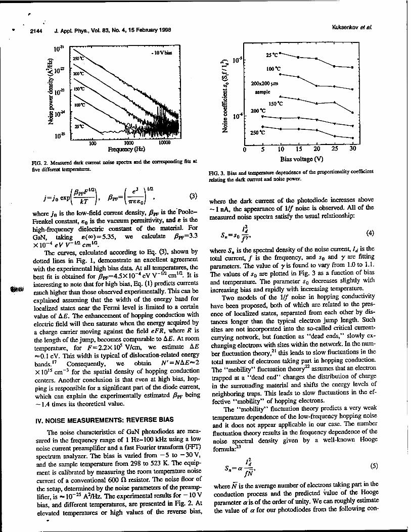
2144 J. Appl. Phys., Vol. 83, No. 4,15 February 1998 Kuksenkov et a/.
100 1000 10000 Frequency (lb)
FIG. 2. Measured dark current noise spectra and the corresponding fits at five different temperatures.
J-J.4*£\. M^P (3)
where jo is the low-field current density, ßw is the Poole- Frenkel constant, c0 is the vacuum permittivity, and e is the high-frequency dielectric constant of die material. For GaN, taking e(°o)=5.35, we calculate ySpF=3.3 X10~* eV V~m cmin.
The curves, calculated according to Eq. (3), shown by dotted lines in Fig. 1, demonstrate an excellent agreement with the experimental high bias data. At all temperatures, the best fit is obtained for y3PF=4.5XlO~4eV V_,/2cm,/2. It is interesting to note that for high bias, Eq. (1) predicts currents much higher than those observed experimentally. This can be explained assuming that the width of the energy band for localized states near the Fermi level is limited to a certain value of A£. The enhancement of hopping conduction with electric field will then saturate when the energy acquired by a charge carrier moving against the field eFR, where R is the length of the jump, becomes comparable to A£. At room temperature, for F=2.2X10S V/cm, we estimate A£ «0.1 eV. This width is typical of dislocation-related energy bands.17 Consequendy, we obtain N'=NAE"*2 X 101S cm-3 for the spatial density of hopping conduction centers. Another conclusion is that even at high bias, hop- ping is responsible for a significant part of the diode current, which can explain the experimentally estimated ySPF being ~ 1.4 times its theoretical value.
IV. NOISE MEASUREMENTS: REVERSE BIAS
The noise characteristics of GaN photodiodes are mea- sured in the frequency range of 1 Hz-100 kHz using a low noise current preamplifier and a fast Fourier transform (FFT) spectrum analyzer. The bias is varied from -5 to -30 V, and the sample temperature from 298 to 523 K. The equip- ment is calibrated by measuring the room temperature noise current of a conventional 600 ft resistor. The noise floor of the setup, determined by the noise parameters of the preamp- lifier, is ~ 10"25 A2/Hz. The experimental results for -10 V bias, and different temperatures, are presented in Fig. 2. At elevated temperatures or high values of the reverse bias,
J~L lO"5
1 8
2 i<f
250*C
0 5 10 15 20 25
Bias voltage (V)
FIG. 3. Bias and temperature dependence of the proportionality coefficient relating the dark current and noise power.
where the dark current of the photodiode increases above ~ 1 nA, the appearance of 1// noise is observed. All of the measured noise spectra satisfy the usual relationship:
Sn=s0
/2
r (4)
where S„ is the spectral density of the noise current, Id is the total current, / is the frequency, and s0 and y are fitting parameters. The value of y is found to vary from 1.0 to 1.1. The values of sQ are plotted in Fig. 3 as a function of bias and temperature. The parameter s0 decreases slightly with increasing bias and rapidly with increasing temperature.
Two models of the 1// noise in hopping conductivity have been proposed, both of which are related to the pres- ence of localized states, separated from each other by dis- tances longer than the typical electron jump length. Such sites are not incorporated into the so-called critical current- carrying network, but function as "dead ends," slowly ex- changing electrons with sites within the network. In the num- ber fluctuation theory,21 this leads to slow fluctuations in the total number of electrons taking part in hopping conduction. The "mobility" fluctuation theory22 assumes that an electron trapped at a "dead end" changes the distribution of charge in the surrounding material and shifts the energy levels of neighboring traps. This leads to slow fluctuations in the ef- fective "mobility" of hopping electrons.
The "mobility" fluctuation theory predicts a very weak temperature dependence of the low-frequency hopping noise and it does not appear applicable in our case. The number fluctuation theory results in the frequency dependence of the noise spectral density given by a well-known Hooge formula:23
S„=ar—, fN
(5)
where N is the average number of electrons taking part in the conduction process and the predicted value of the Hooge parameter a is of the order of unity. We can roughly estimate the value of a for our photodiodes from the following con-

* J. Appl. Phys., Vol. 83. No. 4,15 February 1998 Kuksenkov et al. 2145
co
S.OxlO-5
4.5xl0-'
£ 4.0x10*
«a
1 8 '1
3.5x1 ff5
3.0xW'
Z5xlffJ
"8 ZOxlO"5
1 o
35
Uxlff4
1.0x10* 100 1000 10000
Frequency (Hz)
FIG. 4. Normalized noise spectra at 2 V forward bias and different temperatures.
%
2.6 2.8 3.0 IOOO/T(I/K)
FIG. 5. Arrhenius plot for the trap center lifetime obtained from the mea- sured noise spectra.
sideration. From Eqs. (4) and (5) we have ce=SoN. At room temperature and —10 V reverse bias, the measured value of the parameter sQ is ~1.3X10"S. At the same temperature and bias the dark current of the photodiode is ~ 1 nA, or, equivalently, the sample resistance is J?~lX10l0ft. The number of electrons N can be found from R=L2/(e/iN), where the length L is taken to be equal to the depletion layer width w, obtained from C-V measurements. The effective mobility fi is estimated from the theory of hopping conduction9 using parameters obtained from the fit to the I-V data at room temperature. We obtain fi~5 X10"6 cm2 V"1 s~\ JV~2.3X 10s, and finally, a~3, con- sistent with the predictions of the number fluctuation theory. Both the bias and temperature dependence of the parameter s0 can be explained by the change in the number of hopping electrons N. With increasing bias, N goes up due to increas- ing width of the depletion layer, and with temperature, due to decreasing length of a typical jump.
V. NOISE MEASUREMENTS: FORWARD BIAS
Under a forward bias, the built-in electric field de- creases, and hopping is no longer a dominant conductivity mechanism. The photodiode current is dominated by diffu- sion currents in the neutral region. As a consequence, we do not observe the l/f current noise. Instead, most devices show a very clear g-r noise component with a Lorentzian spec- trum of the form:
*.(«)-A 1+(Uro)». (6)
where A is a constant and r0 is the characteristic time of the generation-recombination process. For the accurate determi- nation of r0 from experimental data, it is convenient to mul- tiply the measured noise density S„ll\ by to-lirf and plot it on a linear scale as a function of frequency /. The Lorentzian then appears as a symmetric peak at/0, and r0 is found from r0=l/2irfo-
In Fig. 4, we plot the frequency dependence of the nor- malized noise density at three different temperatures, mea-
sured on a 200X200 /tm2 device at a forward bias of +2 V. It is clear from Fig. 4 that/0 is increasing and, therefore, T0
is decreasing with temperature. For a thermally activated g-r process the characteristic time r0 is expected to follow an Arrhenius equation:
T0=7ooexp \wf (7)
where Too »s a constant and e is the activation energy. The value of e can be estimated from the slope of logi^f1) plot- ted against the inverse temperature.25 The Arrhenius plot for our device is presented in Fig. 5. We obtain e~0.49 eV, in agreement with the expected activation energy for centers associated with Ga antisite defects in GaN.26
VI. NOISE MEASUREMENTS UNDER ILLUMINATION
We have also performed noise measurements on GaN photodiodes illuminated with a Xe arc lamp. The photodiode bias was kept at —5 V, and the light intensity was adjusted by changing the lamp current. Unfortunately, at low frequen- cies the measured noise was dominated by the noise of the lamp itself, so we do not have experimental evidence for the presence or absence of the l/f noise in the photocurrenL Above —10 kHz, the measured noise spectrum was com- pletely flat The corresponding noise current density is plot- ted in Fig. 6 as a function of photocurrent /,,. Figure 6 shows that the experimental points lie very close to the line of ■Jlelp, expected from the shot noise theory.27 We conclude that, at least at these frequencies, no other significant noise sources are present in photoconduction.
VII. DEVICE PERFORMANCE
At room temperature and for reverse bias values lower than 10 V, the dark current noise spectra disappear below the noise floor of our measurement setup. However, the device performance can be estimated by extrapolating noise data taken at higher biases. The dark current at -3 V is 2.7 pA, resulting in 5n (at 1 Hz) =7.3X 10~29 A2/Hz. At this bias the magnitude of the l/f noise for frequencies above
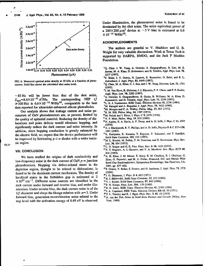
• 2146 J. Appl. Phys., Vol. 83, No. 4,15 February 1998 Kuksenkov et al.
$&;&■'
"23
c u
c
I
FIG. 6. current.
2 25xlff
2.0x10" 0 14 0<i6 o.ig o^O 0.22 054 056 058 030 0.32
Pbotocuirent (uA)
Measured spectral noise density at 20 kHz as a function of photo- Solid line shows the calculated shot noise level.
~85Hz will be lower than that of the shot noise, 5diot~8.6XlO_31 A2/Hz. The corresponding NEP (/ s* 100 Hz) is 6.6X10"'5 W/Hz,/2, comparable to the best data reported for ultraviolet-enhanced silicon photodiodes.
Our analysis shows that leakage current and noise pa- rameters of GaN photodetectors are, at present, limited by the quality of epitaxial material. Reducing the density of dis- locations and point defects would eliminate hopping, and significantly reduce the dark current and noise intensity. In addition, since hopping conduction is greatly enhanced by the electric field, we expect that the device performance will be improved by fabricating p-i-n diodes with a wider intrin- sic region.
VIII. CONCLUSION
We have studied the origins of dark conductivity and low-frequency noise in the dark current of GaN p-n junction photodetectors. Hopping via defect-related states in the depletion region, thought to be related to dislocations, is found to be the dominant current mechanism. The density of localized states in the forbidden gap is estimated at 2 X 1015 cm-3. Different noise sources are identified in the dark current under forward and reverse bias, and under illu- mination. Under reverse bias, the dark current noise is of the \lf character and obeys the Hooge relation with a«* 3. Under forward bias, generation-recombination noise related to the trap level with the activation energy of 0.49 eV is observed.
Under illumination, the photocurrent noise is found to be dominated by the shot noise. The noise equivalent power of a 200X200/tm2 device at -3 V bias is estimated at 6.6 X10_,5W/Hzl/2.
ACKNOWLEDGMENTS
The authors are grateful to V. Mashkov and G. B. Wright for very valuable discussions. Work at Texas Tech is supported by DARPA, BMDO, and the Jack F Maddox Foundation.
'Q. Chen, J. W. Yang, A. Osinsky, S. Gangopadhyay, B. Lim, M. Z. Anwar, M. A. Khan, D. Kuksenkov, and H. Temkin, Appl. Phys. Lett. 70, 2277 (1997).
2F. Binet, J. Y. Duboz, N. Laurent, E. Rosencher, O. Briot, and R. L. Aulombard, J. Appl. Phys. 81, 6449 (1997).
3Q. Chen, M. A. Khan, C. J. Sun, and J. W. Yang, Electron. Leu. 31, 1781 (1995).
4J. M. Van Hove, R. Hickman. J. J. Klaassen, P. P. Chow, and P. P. Ruden, Appl. Phys. Lett. 70, 2282 (1997).
5 A. Osinsky, S. Gangopadhyay, R. Gaska, B. Williams, M. A. Khan, D. Kuksenkov, and H. Temkin, Appl. j»hys. Lett. 71, 2334 (1997).
6L. K. J. Vandamme, IEEE Trans. Electron Devices 41, 2176 (1994). 7M. Razeghi and A. Rogalski. J. Appl. Phys. 79, 7433 (1996). *M. Morgan and P. A. Walley, Philos. Mag. 23, 661 (1971). »R. M. Hill, Philos. Mag. 24, 1307 (1971).
I0M. Pollak and I. Riess, J. Phys. C 9, 2339 (1976). "N. F. Mott, Philos. Mag. 19, 835 (1969). ,2N. Aspley, E. A. Davis, A. P. Troup, and A. D. Ioffe, J. Phys. C 11.4983
(1978). 13 A. J. Mackintosh, R. T. Phillips, and A. D. Ioffe. Physica B & C 117-118,
1001 (1983). 14 K. Kuriyama, K. Kazama, T. Koyama, T. Takamori. and T. Kamijoh,
Solid State Commun. 103, 145 (1997). 15M. L. Knotek. M. Pollak, T. M. Donovan, and H. Kurtzmann, Phys. Rev.
Lett. 30, 854 (1973). I6C. H. Seager and G. E. Pike, Phys. Rev. B 10, 1435 (1974). 17 N. T. Bagraev, A. I. Gusarov, and V. A. Mashkov, Sov. Phys. JETP 68,
816 (1989). 18 A. H. Khan, J. M. Meese, T. Stacy, E. M. Charlson, E. J. Charlson, G.
Zhao, G. Popovici. and M. A. Prelas, Diamond, SiC, and Nitride Wide Band Gap Semiconductors, Symposium Proceedings, San Francisco, CA, 1994, pp. 637-642.
"P. Gonon, Y. Boiko, S. Prawer, and D. Jamieson, J. Appl. Phys. 79, 3778 (1996).
^J. G. Simmons, J. Phys. D 4, 613 (1971). 21B. I. Shklovskii, Solid State Commun. 33, 273 (1980). 22 V. I. Kozub, Solid State Commun. 97, 843 (1996). ^F. N. Hooge, Phys. Lett. 29A, 139 (1969). 24 B. K. Jones, IEEE Trans. Electron Devices 41, 2188 (1994). "J. A. Copeland, IEEE Trans. Electron Devices ED-18. 50 (1971). *T. L. Tansley and R. J. Egan, Phys. Rev. B 45, 10 (1993). "A. van der Ziel, Noüe in Solid State Devices and Circuits (Wiley, New
York, 1986).


![[123doc.vn] Bai Tap Trac Nghiem Tieng Anh 12 Tu Bai de Bai 7 0476](https://static.fdocuments.net/doc/165x107/55cf8f51550346703b9b23a1/123docvn-bai-tap-trac-nghiem-tieng-anh-12-tu-bai-de-bai-7-0476.jpg)
