WAVEGUIDES; RESONATORS, LINES, OR OTHER DEVICES OF THE ... · transmission of energy. Waveguide...
84
CPC - H01P - 2020.01 H01P WAVEGUIDES; RESONATORS, LINES, OR OTHER DEVICES OF THE WAVEGUIDE TYPE (operating at optical frequencies G02B ; aerials H01Q ; {modulating electromagnetic waves in transmission line, waveguide, cavity resonator or radiation field of aerial H03C 7/02 }; networks comprising lumped impedance elements H03H ) Definition statement This place covers: Passive devices which have electrical dimensions comparable with the working wavelength, and which operate at frequencies up to but not including optical frequencies, e.g. microwave, and their manufacture. Auxiliary devices of waveguide type such as filters, phase shifters, non-reciprocal devices, polarisation rotators. Tubular waveguides and transmission lines such as strip lines, microstrips, coaxial lines, dielectric waveguides. Devices for coupling between waveguides, transmission lines or waveguide type devices. Resonators of the waveguide type. Delay lines of the waveguide type. Apparatus or processes specially adapted for manufacturing waveguides, transmission lines, or waveguide type devices. Relationships with other classification places Waveguides and waveguide type devices are commonly associated with antennas and aerials, these are classified in H01Q . H01P is concerned with individual circuit components, or basic combinations of them. More complicated networks with lumped impedance elements are classified in H03H . References Limiting references This place does not cover: Devices operating at optical frequencies G02B Informative references Attention is drawn to the following places, which may be of interest for search: Coaxial cables H01B 11/18 Transit-time tubes H01J 23/00 Aerials H01Q Quasi-optical devices H01Q 15/00 Line connectors H01R Cable fittings H02G 15/00 Networks comprising lumped impedance elements H03H 1
Transcript of WAVEGUIDES; RESONATORS, LINES, OR OTHER DEVICES OF THE ... · transmission of energy. Waveguide...

CPC - H01P - 2020.01
H01P
WAVEGUIDES; RESONATORS, LINES, OR OTHER DEVICES OF THEWAVEGUIDE TYPE (operating at optical frequencies G02B; aerials H01Q;{modulating electromagnetic waves in transmission line, waveguide, cavityresonator or radiation field of aerial H03C 7/02}; networks comprising lumpedimpedance elements H03H)
Definition statement
This place covers:
Passive devices which have electrical dimensions comparable with the working wavelength, andwhich operate at frequencies up to but not including optical frequencies, e.g. microwave, and theirmanufacture.
Auxiliary devices of waveguide type such as filters, phase shifters, non-reciprocal devices, polarisationrotators.
Tubular waveguides and transmission lines such as strip lines, microstrips, coaxial lines, dielectricwaveguides.
Devices for coupling between waveguides, transmission lines or waveguide type devices.
Resonators of the waveguide type.
Delay lines of the waveguide type.
Apparatus or processes specially adapted for manufacturing waveguides, transmission lines, orwaveguide type devices.
Relationships with other classification places
Waveguides and waveguide type devices are commonly associated with antennas and aerials, theseare classified in H01Q.
H01P is concerned with individual circuit components, or basic combinations of them. Morecomplicated networks with lumped impedance elements are classified in H03H.
References
Limiting references
This place does not cover:
Devices operating at optical frequencies G02B
Informative references
Attention is drawn to the following places, which may be of interest for search:
Coaxial cables H01B 11/18
Transit-time tubes H01J 23/00
Aerials H01Q
Quasi-optical devices H01Q 15/00
Line connectors H01R
Cable fittings H02G 15/00
Networks comprising lumped impedance elements H03H
1
H01P (continued) CPC - H01P - 2020.01
Glossary of terms
In this place, the following terms or expressions are used with the meaning indicated:
Auxiliary devices Devices which perform an operation other than the mere simpletransmission of energy.
Waveguide type As applied to transmission lines, this term includes only high-frequency coaxial cables or Lecher lines, and as applied toresonators, delay lines, or other devices, this term includes alldevices having distributed inductance and capacitance.
Synonyms and Keywords
In patent documents, the following abbreviations are often used:
Non-reciprocal devices Components such as circulators or isolators, using the propagationproperties of ferrites.
H01P 1/00
Auxiliary devices (coupling devices of the waveguide type H01P 5/00)
Definition statement
This place covers:
Devices which perform an operation other than the mere simple transmission of energy.
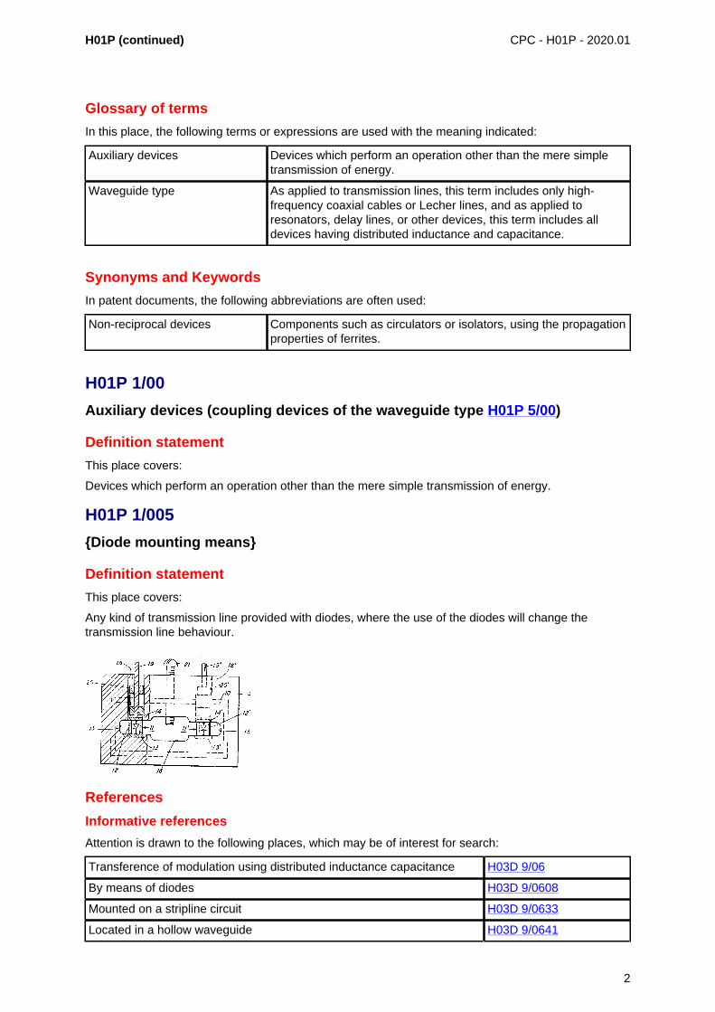
H01P 1/005
{Diode mounting means}
Definition statement
This place covers:
Any kind of transmission line provided with diodes, where the use of the diodes will change thetransmission line behaviour.
References
Informative references
Attention is drawn to the following places, which may be of interest for search:
Transference of modulation using distributed inductance capacitance H03D 9/06
By means of diodes H03D 9/0608
Mounted on a stripline circuit H03D 9/0633
Located in a hollow waveguide H03D 9/0641
2
CPC - H01P - 2020.01
H01P 1/02
Bends; Corners; Twists
Definition statement
This place covers:
Illustrative example of subject matter classified in H01P 1/02:
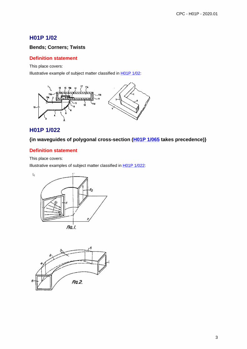
H01P 1/022
{in waveguides of polygonal cross-section (H01P 1/065 takes precedence)}
Definition statement
This place covers:
Illustrative examples of subject matter classified in H01P 1/022:
3
CPC - H01P - 2020.01
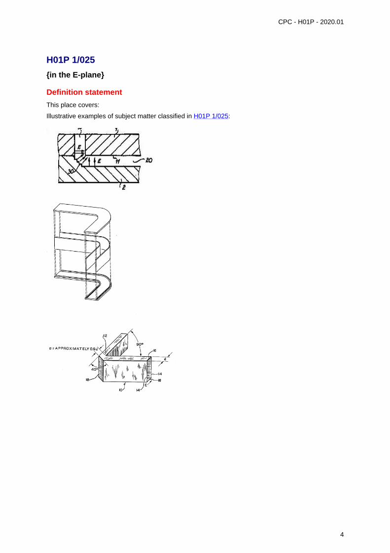
H01P 1/025
{in the E-plane}
Definition statement
This place covers:
Illustrative examples of subject matter classified in H01P 1/025:
4
CPC - H01P - 2020.01
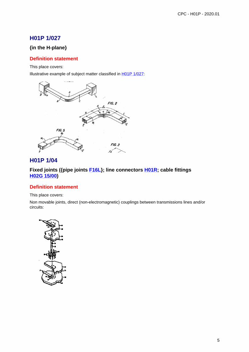
H01P 1/027
{in the H-plane}
Definition statement
This place covers:
Illustrative example of subject matter classified in H01P 1/027:
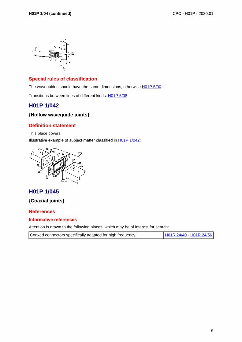
H01P 1/04
Fixed joints ({pipe joints F16L}; line connectors H01R; cable fittingsH02G 15/00)
Definition statement
This place covers:
Non movable joints, direct (non-electromagnetic) couplings between transmissions lines and/orcircuits:
5
H01P 1/04 (continued) CPC - H01P - 2020.01
Special rules of classification
The waveguides should have the same dimensions, otherwise H01P 5/00.
Transitions between lines of different kinds: H01P 5/08
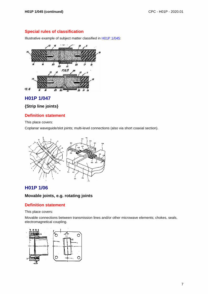
H01P 1/042
{Hollow waveguide joints}
Definition statement
This place covers:
Illustrative example of subject matter classified in H01P 1/042:
H01P 1/045
{Coaxial joints}
References
Informative references
Attention is drawn to the following places, which may be of interest for search:
Coaxed connectors specifically adapted for high frequency H01R 24/40 - H01R 24/56
6
H01P 1/045 (continued) CPC - H01P - 2020.01
Special rules of classification
Illustrative example of subject matter classified in H01P 1/045:
H01P 1/047
{Strip line joints}
Definition statement
This place covers:
Coplanar waveguide/slot joints; multi-level connections (also via short coaxial section).
H01P 1/06
Movable joints, e.g. rotating joints
Definition statement
This place covers:
Movable connections between transmission lines and/or other microwave elements; chokes, seals,electromagnetical coupling.
7
H01P 1/06 (continued) CPC - H01P - 2020.01
Special rules of classification
Variable degree of coupling between transmission lines: H01P 5/04; Flexible waveguides: H01P 3/14.
H01P 1/061
{the relative movement being a translation along an axis common to at leasttwo rectilinear parts, e.g. expansion joints}
Definition statement
This place covers:
Illustrative example of subject matter classified in H01P 1/061:
H01P 1/062
{the relative movement being a rotation}
Definition statement
This place covers:
Illustrative example of subject matter classified in H01P 1/062:
Special rules of classification
Using mechanical rotation for polarisation rotation: H01P 1/165.
8
CPC - H01P - 2020.01
H01P 1/064
{the axis of rotation being perpendicular to the transmission path, e.g. hingejoint}
Definition statement
This place covers:
Illustrative example of subject matter classified in H01P 1/064 :
H01P 1/065
{the axis of rotation being parallel to the transmission path, e.g. stepped twist}
Definition statement
This place covers:
Illustrative examples of subject matter classified in H01P 1/065:
9
CPC - H01P - 2020.01
H01P 1/066
{with an unlimited angle of rotation}
Definition statement
This place covers:
Illustrative examples of subject matter classified in H01P 1/062:
H01P 1/067
{the energy being transmitted in only one line located on the axis of rotation}
Definition statement
This place covers:
Illustrative example of subject matter classified in H01P 1/067:
10
CPC - H01P - 2020.01
H01P 1/068
{the energy being transmitted in at least one ring-shaped transmissionline located around the axis of rotation, e.g. "around the mast" rotary joint(H01P 1/069 takes precedence; coaxial line with solid inner conductorH01P 1/067)}
Definition statement
This place covers:
Illustrative example of subject matter classified in H01P 1/068:
H01P 1/069
{the energy being transmitted in at least one ring-shaped transmission linelocated around an axial transmission line; Concentric coaxial systems}
Definition statement
This place covers:
Illustrative examples of subject matter classified in H01P 1/069 :
H01P 1/08
Dielectric windows (coupling devices for transit time tubes H01J 23/36)
Definition statement
This place covers:
Aperture in a waveguide to insulate microwave circuits from differential pressures, but they enable thepropagation of microwaves without introducing reflection or internal resonance.
Windows of the kind which serve to isolate the environment without a section of electromagnetictransmission line from another environment of different pressures and/or other environmental
11
H01P 1/08 (continued) CPC - H01P - 2020.01
conditions, and which allow electromagnetic energy travelling along the transmission line to passthrough the window with little or no loss of power.
H01P 1/10
for switching or interrupting {(in systems using reflection or reradiation ofradio, acoustic or other waves G01S 7/034)}
Relationships with other classification places
• H01H (related to switches);
• H01H 59/00 (MEM's).
Glossary of terms
In this place, the following terms or expressions are used with the meaning indicated:
MEM Microelectromechanical (switches)
BAW Bulk Acoustic Wave
H01P 1/11
by ferromagnetic devices
Definition statement
This place covers:
Anisotropic media: Media where the vectors E and D are nonparallel and/or nonparallel H and Bvectors, which means that the media has different electrical properties in different directions, and thusthe permittivity and/or permeability has a matrix form.
Ferrites are ferromagnetic ceramic materials, compounds of iron, boron and barium or strontiumor molybdenum. Ferrites have a high magnetic permeability, which allows them to store strongermagnetic fields than iron, and are known as ceramic magnets.
12
H01P 1/11 (continued) CPC - H01P - 2020.01
Applying a DC magnetic bias field to a ferrite will produce that a microwave signal will propagatedifferently in different directions, this effect can be utilized to fabricate directional devices as isolators,circulators and gyrators. The interaction with an applied microwave signal can be controlled byadjusting the strength of the bias field, which leads to a variety of control devices such as phaseshifters, switches and tunable resonators and filters.
H01P 1/12
by mechanical chopper
Definition statement
This place covers:
Mechanical switches (can be electrically or magnetically controlled); redundancy switches; distributionof signals; channel selection; also mechanical aspects of switchable attenuators, filters, etc.; chokingaspects.
Relationships with other classification places
MEMS in H01H 1/0036, H01H 59/0009.
13
CPC - H01P - 2020.01
H01P 1/122
{Waveguide switches}
Definition statement
This place covers:
Illustrative examples of subject matter classified in H01P 1/122:
H01P 1/125
{Coaxial switches}
Definition statement
This place covers:
Illustrative examples of subject matter classified in H01P 1/125:
14

CPC - H01P - 2020.01
H01P 1/127
{Strip line switches}
Definition statement
This place covers:
Illustrative example of subject matter classified in H01P 1/127:
Relationships with other classification places
MEMS in H03H 9/2405 and H03H 3/0072.
H01P 1/14
by electric discharge devices (discharge devices H01J 17/64)
Definition statement
This place covers:
Triggering plasma; multipactor switch; generating electron beams; use as receiver protector.
15

CPC - H01P - 2020.01
H01P 1/15
by semiconductor devices
Definition statement
This place covers:
(varactor) diodes; optically controlled semiconductors; use as transmit/receive switch.
References
Limiting references
This place does not cover:
Optically controlled G02B 6/00
Electronic switching or gating...in bipolar transistor switches; H03K 17/04126
Electronic switching or gating....switching arrangements with severalinput- or output-terminals.
H03K 17/04126
Switches using semiconductor devices H03K 17/56
Using Fets, Field effect transistors H03K 17/687
Using Diodes H03K 17/74
16
CPC - H01P - 2020.01
H01P 1/16
for mode selection, e.g. mode suppression or mode promotion; for modeconversion (linking dissimilar lines or devices H01P 5/08)
Definition statement
This place covers:
Illustrative example of subject matter classified in H01P 1/16:
H01P 1/161
sustaining two independent orthogonal modes, e.g. orthomode transducer{(combining or separating polarisations and frequencies H01P 1/2131)}
Definition statement
This place covers:
Orthomode transducer: a three port waveguide device which supports signals having two orthogonalmodes.
References
Limiting references
This place does not cover:
Orthomode horns H01Q 13/0258
17

CPC - H01P - 2020.01
H01P 1/162
absorbing spurious or unwanted modes of propagation
Definition statement
This place covers:
Illustrative examples of subject matter classified in H01P 1/162:
H01P 1/165
for rotating the plane of polarisation
Definition statement
This place covers:
Illustrative example of subject matter classified in H01P 1/16:
References
Limiting references
This place does not cover:
Rotation in free space H01Q 15/246,H01Q 21/245
18
CPC - H01P - 2020.01
H01P 1/17
for producing a continuously rotating polarisation, e.g. circular polarisation
Definition statement
This place covers:
linear <--> circular polarisation; (gradual) change of waveguide inner surface; meandering conductorsin a waveguide.
Relationships with other classification places
See also H01Q 15/244.
H01P 1/171
{using a corrugated or ridged waveguide section}
Definition statement
This place covers:
Illustrative examples of subject matter classified in H01P 1/171:
H01P 1/172
{using a dielectric element}
Definition statement
This place covers:
Illustrative examples of subject matter classified in H01P 1/172:
19
CPC - H01P - 2020.01
H01P 1/173
{using a conductive element}
Definition statement
This place covers:
Illustrative example of subject matter classified in H01P 1/173:
H01P 1/174
{using a magnetic element (H01P 1/175 takes precedence)}
Definition statement
This place covers:
Illustrative examples of subject matter classified in H01P 1/174:
H01P 1/175
using Faraday rotators
Definition statement
This place covers:
Faraday rotation is the rotation of the plane of polarization of microwave energy exhibited when theenergy is transmitted through ferrite material in the direction of a magnetic field.
A ferrite rod is included within the waveguide and is usually surrounded by an electrical coil to providea magnetic field. By adjusting the plane of polarisation of the microwave radiation, its propagationalong the waveguide may be controlled.
20

CPC - H01P - 2020.01
H01P 1/18
Phase-shifters (H01P 1/165 takes precedence; coupling devices with variablecoupling factor H01P 5/04)
Definition statement
This place covers:
Illustrative example of subject matter classified in H01P 1/18:
Relationships with other classification places
see also H01Q 3/36, H01Q 3/38.
Phase-inverters used in push-pull amplifiers: H03F 3/26, H03F 3/30.
H01P 1/181
{using ferroelectric devices}
Definition statement
This place covers:
Illustrative example of subject matter classified in H01P 1/181.
21

CPC - H01P - 2020.01
H01P 1/182
{Waveguide phase-shifters (H01P 1/181, H01P 1/185, H01P 1/19 takeprecedence)}
Definition statement
This place covers:
Illustrative examples of subject matter classified in H01P 1/182.
H01P 1/183
{Coaxial phase-shifters (H01P 1/181, H01P 1/185, H01P 1/19 take precedence)}
Definition statement
This place covers:
Illustrative examples of subject matter classified in H01P 1/18.
H01P 1/184
{Strip line phase-shifters (H01P 1/181, H01P 1/185, H01P 1/19 take precedence)}
Definition statement
This place covers:
22
H01P 1/184 (continued) CPC - H01P - 2020.01
Microstrip, slotlines, coplanar lines phase shifters are included in this group.
H01P 1/185
using a diode or a gas filled discharge tube
Definition statement
This place covers:
Illustrative examples of subject matter classified in H01P 1/185:
References
Informative references
Attention is drawn to the following places, which may be of interest for search:
Modulating electromagnetic waves using semiconductor devices H03C 7/027
H01P 1/19
using a ferromagnetic device
Definition statement
This place covers:
Non-reciprocal devices; ferrites.
23
H01P 1/19 (continued) CPC - H01P - 2020.01
References
Informative references
Attention is drawn to the following places, which may be of interest for search:
Continuous tuning without displacement of reactive element H03J 3/16
By discharge tube or semiconductor devices simulating variablereactance
H03J 3/18
H01P 1/195
having a toroidal shape
Definition statement
This place covers:
Illustrative examples of subject matter classified in H01P 1/195:
H01P 1/20
Frequency-selective devices, e.g. filters ({variable impedance transformers,e.g. slug tuners or stub tuners H01P 5/04}; resonators H01P 7/00)
Definition statement
This place covers:
This classification is very general, only related to filters that can not be clearly included in any ofthe following classifications or to theoretic articles/application where no specific filter arrangement(microstrip, stripline, waveguide, coaxial, coplanar, etc...) has been specified.
24
H01P 1/20 (continued) CPC - H01P - 2020.01
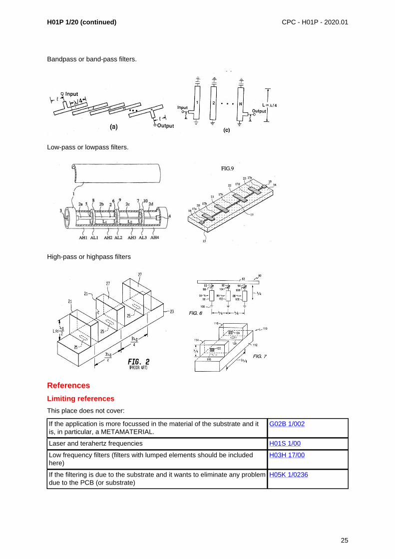
Bandpass or band-pass filters.
Low-pass or lowpass filters.
High-pass or highpass filters
References
Limiting references
This place does not cover:
If the application is more focussed in the material of the substrate and itis, in particular, a METAMATERIAL.
G02B 1/002
Laser and terahertz frequencies H01S 1/00
Low frequency filters (filters with lumped elements should be includedhere)
H03H 17/00
If the filtering is due to the substrate and it wants to eliminate any problemdue to the PCB (or substrate)
H05K 1/0236
25
H01P 1/20 (continued) CPC - H01P - 2020.01
Synonyms and Keywords
In patent documents, the following words/expressions are often used as synonyms:
• "Bandpass" and "band-pass"
• "Low-pass" and "lowpass"
• "Band-stop or bandstop", "band reject","notch filter" and "band elimination"
• "High-pass" and "highpass filter"
H01P 1/2002
{Dielectric waveguide filters (H01P 1/212, H01P 1/213, H01P 1/215, H01P 1/219take precedence)}
Definition statement
This place covers:
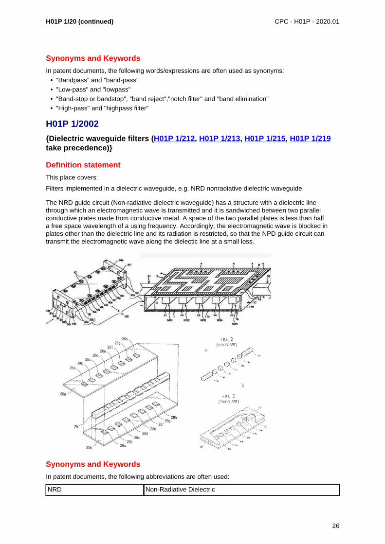
Filters implemented in a dielectric waveguide, e.g. NRD nonradiative dielectric waveguide.
The NRD guide circuit (Non-radiative dielectric waveguide) has a structure with a dielectric linethrough which an electromagnetic wave is transmitted and it is sandwiched between two parallelconductive plates made from conductive metal. A space of the two parallel plates is less than halfa free space wavelength of a using frequency. Accordingly, the electromagnetic wave is blocked inplates other than the dielectric line and its radiation is restricted, so that the NPD guide circuit cantransmit the electromagnetic wave along the dielectic line at a small loss.
Synonyms and Keywords
In patent documents, the following abbreviations are often used:
NRD Non-Radiative Dielectric
26

CPC - H01P - 2020.01
H01P 1/2005
{Electromagnetic photonic bandgaps [EPB], or photonic bandgaps [PBG]}
Definition statement
This place covers:
A structure that possesses a dispersion relation having a bandgap in which propagation ofelectromagnetic waves is prohibited in a specified frequency band is called an electromagneticbandgap structure.
A photonic bandgap structure is a periodic arrangement of "defects" (e.g., pits or holes formed in layerof a device) that prevents the propagation of all electromagnetic waves within a particular frequencyband. The defects introduce electrical frequency stop-bands much like a Bragg grating or crystallattice structure introduces stop-bands in an optical transmission system. The spacing of the photonicbandgap structure's periodic defects determines the stop-band frequencies.
An electromagnetic bandgap* structure (EBG) is recently receiving attention as a scheme to solvesome noise problems in microwave applications. This is for the purpose of blocking a signal ranging acertain frequency band by arranging the EBG having a certain structure in a printed circuit board, andthe typical EBG has roughly two, namely a Mushroom type EBG(MT-EBG) and a Planar type EBG(PT-EBG).
* To have a better explanation of the electromagnetic bandgaps, see XP11037787, XP1034579
Relationships with other classification places
H01Q 15/00:
This EBG structure functions as a magnetic wall that reflects incident electromagnetic waves in phasein the vicinity of the band gap frequency band. For this reason, by installing the EBG structure on theback surface of an antenna, it is possible to achieve a lower profile of the antenna while maintaining itsradiation efficiency.
(Internal Note: reference is made to KW: 1500C5E included in H01Q)
H05K 1/0236: Frequency selective surfaces to shield the noise coming from inside the PCB.
When meta materials are included in the PCB see H05K 1/024.
The metamaterial is an artificial substance having an electromagnetic or optical characteristic whichis not provided in substances existing in the natural world. Representative characteristics of such ametamaterial include negative magnetic permeability ([mu]<0), negative dielectric constant ([elementof]<0), or negative refractive index (in a case where both of the magnetic permeability and thedielectric constant are negative).
Glossary of terms
In this place, the following terms or expressions are used with the meaning indicated:
EBG Electromagnetic Bandgap
PBG Photonic Bandgaps
27
CPC - H01P - 2020.01
H01P 1/2007
{Filtering devices for biasing networks or DC returns}
Definition statement
This place covers:
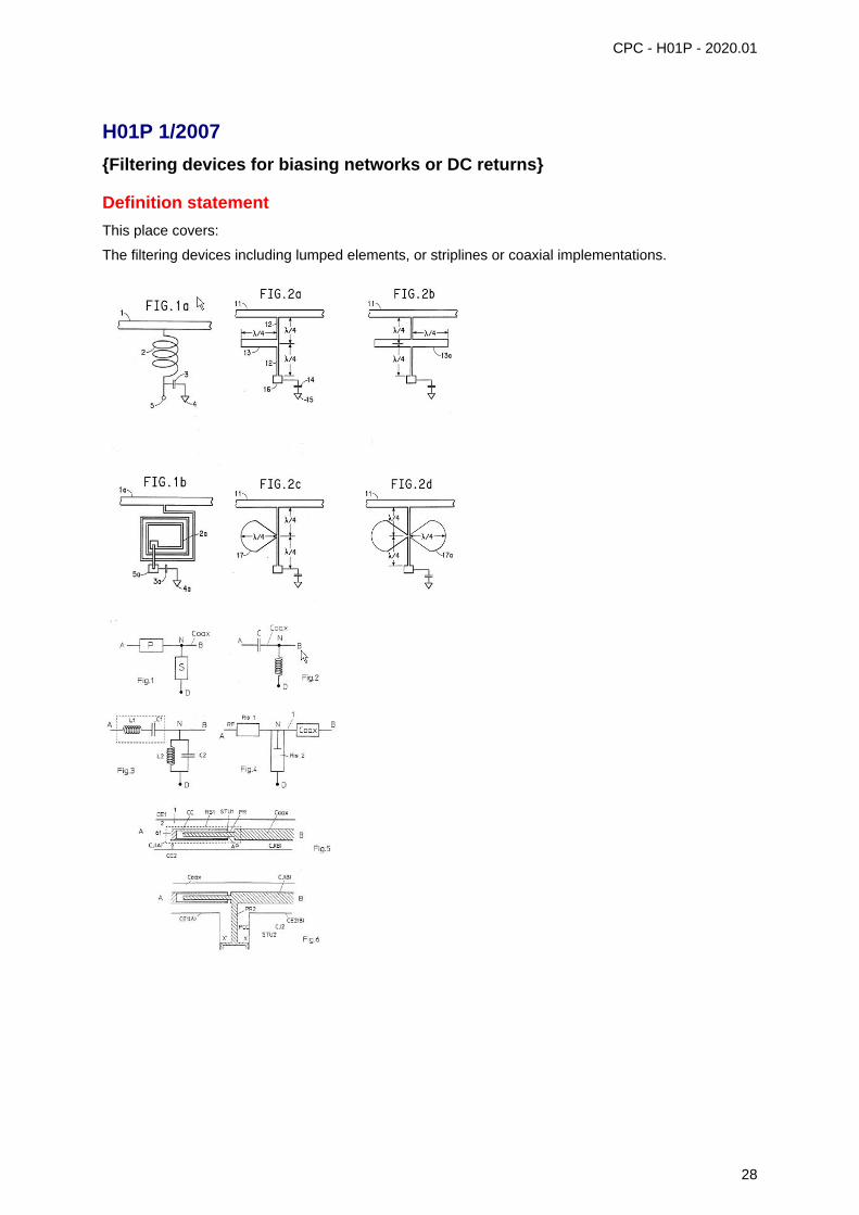
The filtering devices including lumped elements, or striplines or coaxial implementations.
28
CPC - H01P - 2020.01
H01P 1/201
Filters for transverse electromagnetic waves (H01P 1/212, H01P 1/213,H01P 1/215, H01P 1/219 take precedence)
Definition statement
This place covers:
One input and one output frequency (filtered).
The basic transverse electromagnetic wave involves both a varying electric field and a varyingmagnetic field, appearing at right angles to each other and to the direction of travel of the wave.
H01P 1/2013
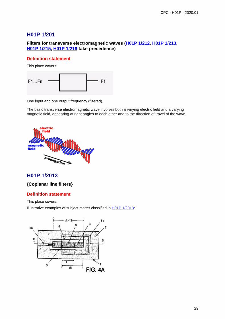
{Coplanar line filters}
Definition statement
This place covers:
Illustrative examples of subject matter classified in H01P 1/2013:
29
H01P 1/2013 (continued) CPC - H01P - 2020.01
H01P 1/2016
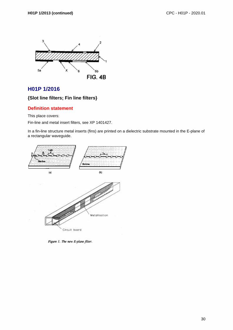
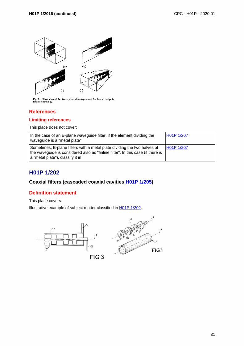
{Slot line filters; Fin line filters}
Definition statement
This place covers:
Fin-line and metal insert filters, see XP 1401427.
In a fin-line structure metal inserts (fins) are printed on a dielectric substrate mounted in the E-plane ofa rectangular waveguide.
30
H01P 1/2016 (continued) CPC - H01P - 2020.01
References
Limiting references
This place does not cover:
In the case of an E-plane waveguide filter, if the element dividing thewaveguide is a "metal plate"
H01P 1/207
Sometimes, E-plane filters with a metal plate dividing the two halves ofthe waveguide is considered also as "finline filter". In this case (if there isa "metal plate"), classify it in
H01P 1/207
H01P 1/202
Coaxial filters (cascaded coaxial cavities H01P 1/205)
Definition statement
This place covers:
Illustrative example of subject matter classified in H01P 1/202.
31

CPC - H01P - 2020.01
H01P 1/203
Strip line filters
Definition statement
This place covers:
Illustrative examples of subject matter classified in H01P 1/203.
References
Limiting references
This place does not cover:
SAW (Surface Acoustic Wave) filters H03H 9/64
32

CPC - H01P - 2020.01
H01P 1/20309
{with dielectric resonator}
Definition statement
This place covers:
Illustrative example of subject matter classified in H01P 1/20309.
H01P 1/20318
{with dielectric resonators as non-metallised opposite openings in themetallised surfaces of a substrate}
Definition statement
This place covers:
Illustrative example of subject matter classified in H01P 1/20318:
33
CPC - H01P - 2020.01
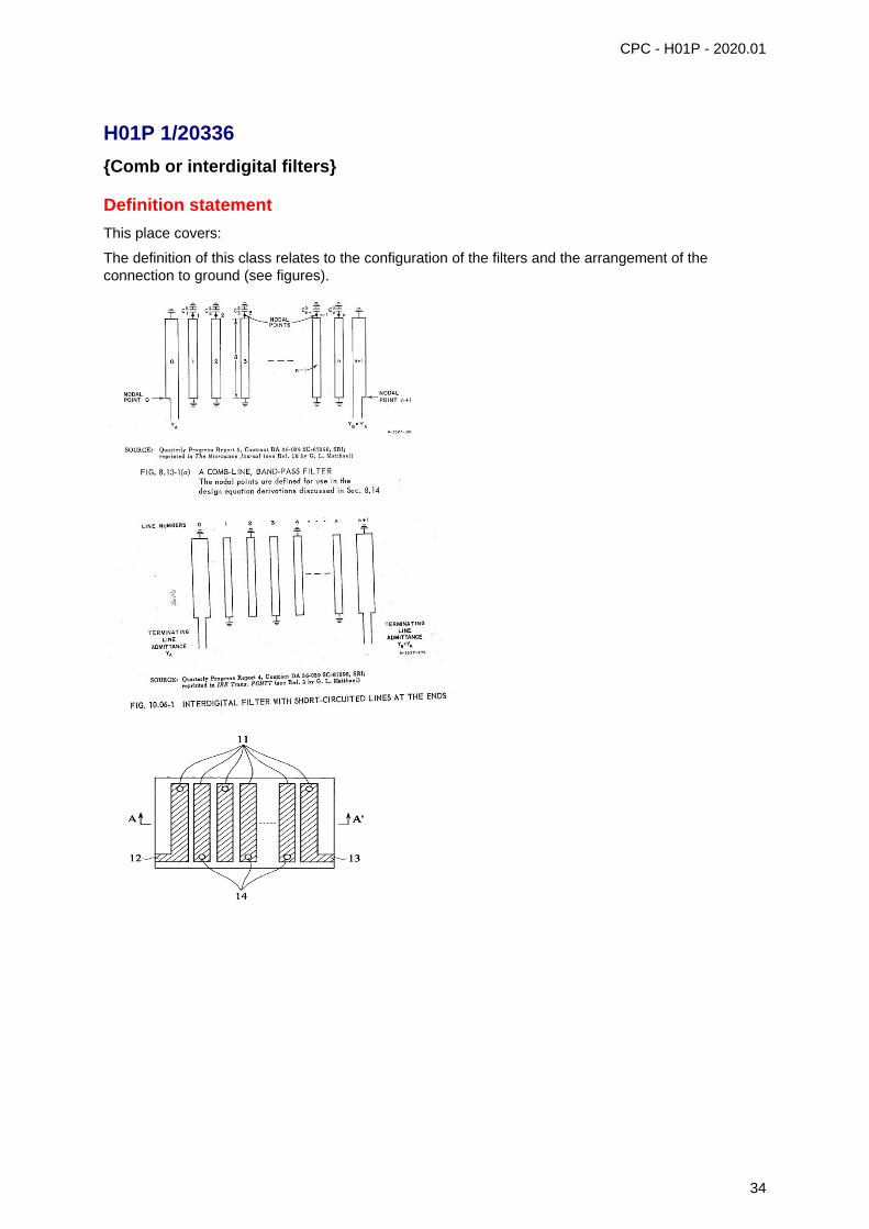
H01P 1/20336
{Comb or interdigital filters}
Definition statement
This place covers:
The definition of this class relates to the configuration of the filters and the arrangement of theconnection to ground (see figures).
34

H01P 1/20336 (continued) CPC - H01P - 2020.01
H01P 1/20345
{Multilayer filters}
Definition statement
This place covers:
The filters are arranged in a plurality of stacked layers, where "usually" the ground planes are theexternal (bottom/top layers) ones.
35
CPC - H01P - 2020.01
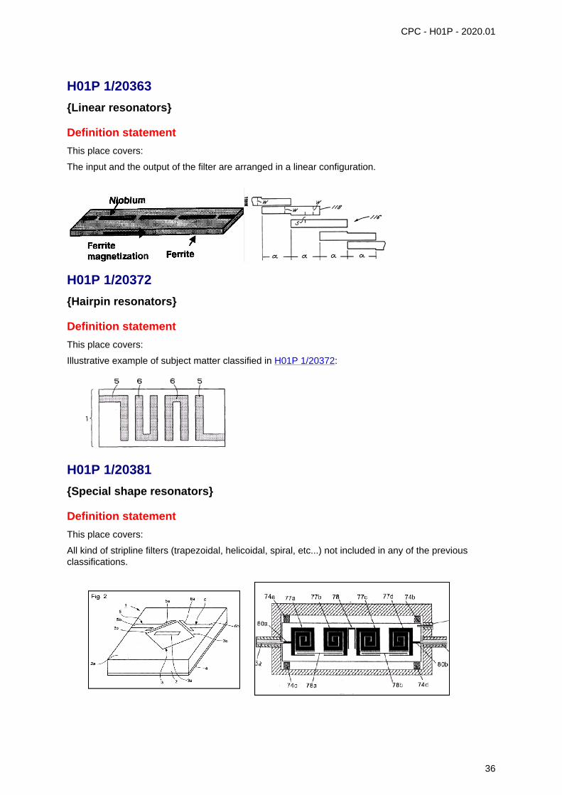
H01P 1/20363
{Linear resonators}
Definition statement
This place covers:
The input and the output of the filter are arranged in a linear configuration.
H01P 1/20372
{Hairpin resonators}
Definition statement
This place covers:
Illustrative example of subject matter classified in H01P 1/20372:
H01P 1/20381
{Special shape resonators}
Definition statement
This place covers:
All kind of stripline filters (trapezoidal, helicoidal, spiral, etc...) not included in any of the previousclassifications.
36

CPC - H01P - 2020.01
H01P 1/2039
{Galvanic coupling between Input/Output}
Definition statement
This place covers:
Low pass filter.
notch, bandstop filter
Bandpass filters using ring resonators with different notch frequencies connected in parallel (seeUS2007/0063794).
37
H01P 1/2039 (continued) CPC - H01P - 2020.01
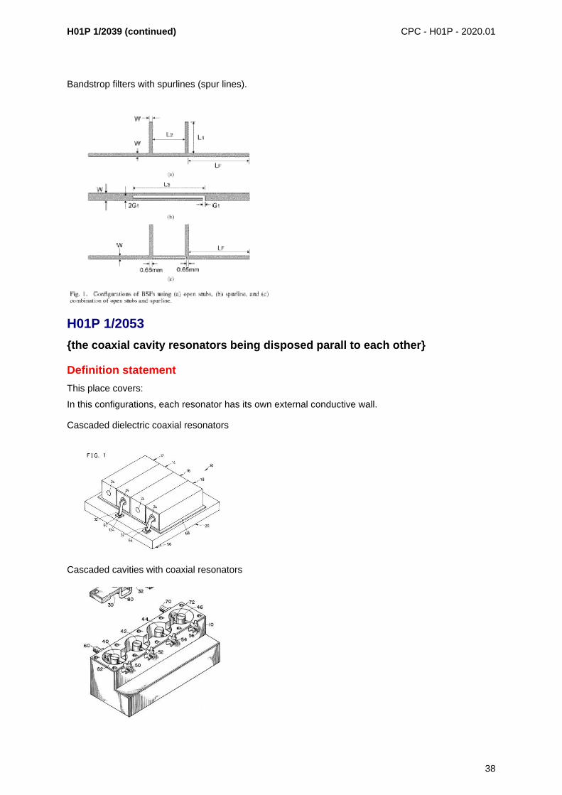
Bandstrop filters with spurlines (spur lines).
H01P 1/2053
{the coaxial cavity resonators being disposed parall to each other}
Definition statement
This place covers:
In this configurations, each resonator has its own external conductive wall.
Cascaded dielectric coaxial resonators
Cascaded cavities with coaxial resonators
38
CPC - H01P - 2020.01
H01P 1/2056
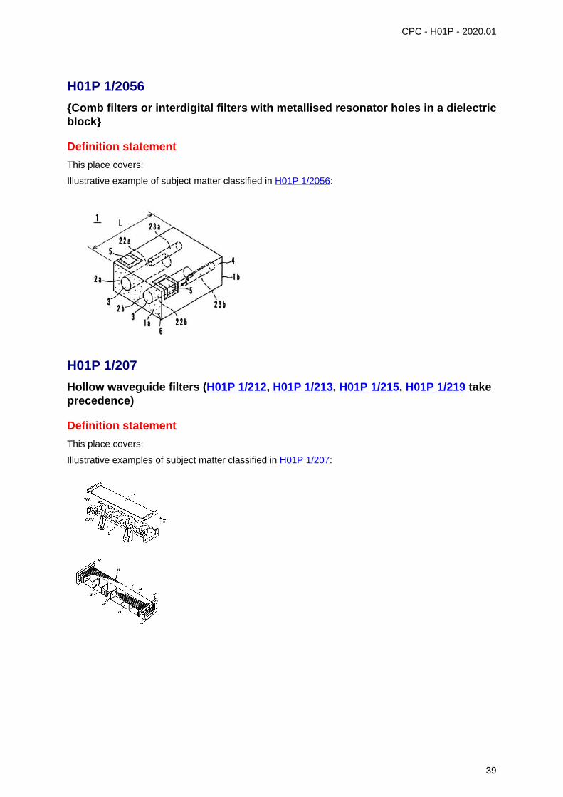
{Comb filters or interdigital filters with metallised resonator holes in a dielectricblock}
Definition statement
This place covers:
Illustrative example of subject matter classified in H01P 1/2056:
H01P 1/207
Hollow waveguide filters (H01P 1/212, H01P 1/213, H01P 1/215, H01P 1/219 takeprecedence)
Definition statement
This place covers:
Illustrative examples of subject matter classified in H01P 1/207:
39
CPC - H01P - 2020.01
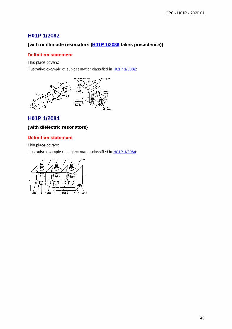
H01P 1/2082
{with multimode resonators (H01P 1/2086 takes precedence)}
Definition statement
This place covers:
Illustrative example of subject matter classified in H01P 1/2082:
H01P 1/2084
{with dielectric resonators}
Definition statement
This place covers:
Illustrative example of subject matter classified in H01P 1/2084:
40
CPC - H01P - 2020.01
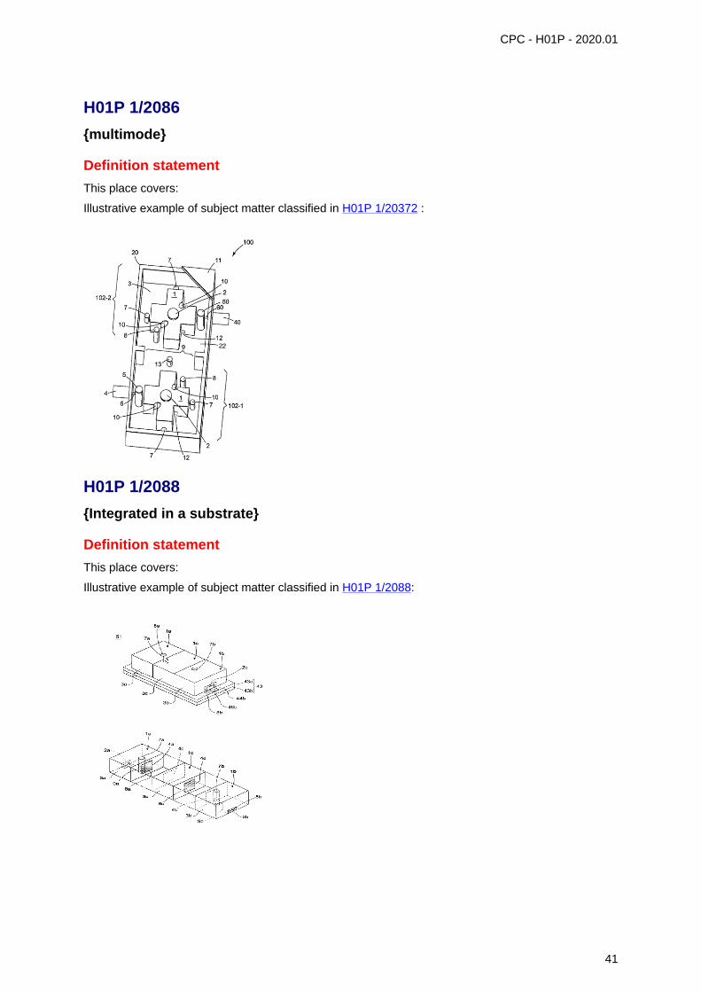
H01P 1/2086
{multimode}
Definition statement
This place covers:
Illustrative example of subject matter classified in H01P 1/20372 :
H01P 1/2088
{Integrated in a substrate}
Definition statement
This place covers:
Illustrative example of subject matter classified in H01P 1/2088:
41

H01P 1/2088 (continued) CPC - H01P - 2020.01
H01P 1/209
comprising one or more branching arms or cavities wholly outside the mainwaveguide
Definition statement
This place covers:
Illustrative example of subject matter classified in H01P 1/209:
H01P 1/211
Waffle-iron filters; Corrugated structures
Definition statement
This place covers:
Illustrative example of subject matter classified in H01P 1/211:
42
H01P 1/211 (continued) CPC - H01P - 2020.01
H01P 1/213
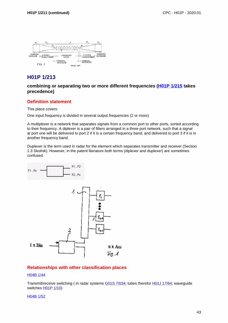
combining or separating two or more different frequencies (H01P 1/215 takesprecedence)
Definition statement
This place covers:
One input frequency is divided in several output frequencies (2 or more)
A multiplexer is a network that separates signals from a common port to other ports, sorted accordingto their frequency. A diplexer is a pair of filters arranged in a three port network, such that a signalat port one will be delivered to port 2 if it is a certain frequency band, and delivered to port 3 if it is inanother frequency band.
Duplexer is the term used in radar for the element which separates transmitter and receiver (Section1.3 Skolnik). However, in the patent literature both terms (diplexer and duplexer) are sometimesconfused.
Relationships with other classification places
H04B 1/44
Transmit/receive switching ( in radar systems G01S 7/034; tubes therefor H01J 17/64; waveguideswitches H01P 1/10)
H04B 1/52
43

H01P 1/213 (continued) CPC - H01P - 2020.01
Hybrid arrangements, i.e. for transition from single-path two-way transmission to single transmissionon each of two path, or vice-versa (multiport networks H03H 7/46; microwave multiplexersH01P 1/213)
H03H 7/46
Networks for connecting several sources or loads, working on different frequencies or frequencybands, to a common load or source (for use in multiplex transmission systems H04J 1/00)
H01P 1/2133
{using coaxial filters (H01P 1/2131, H01P 1/2136 take precedence)}
Definition statement
This place covers:
Illustrative example of subject matter classified in H01P 1/2133:
44
CPC - H01P - 2020.01
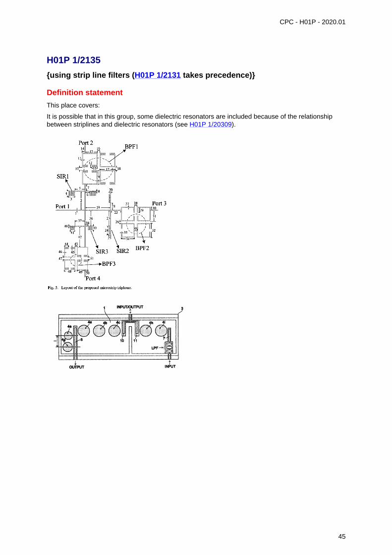
H01P 1/2135
{using strip line filters (H01P 1/2131 takes precedence)}
Definition statement
This place covers:
It is possible that in this group, some dielectric resonators are included because of the relationshipbetween striplines and dielectric resonators (see H01P 1/20309).
45
CPC - H01P - 2020.01
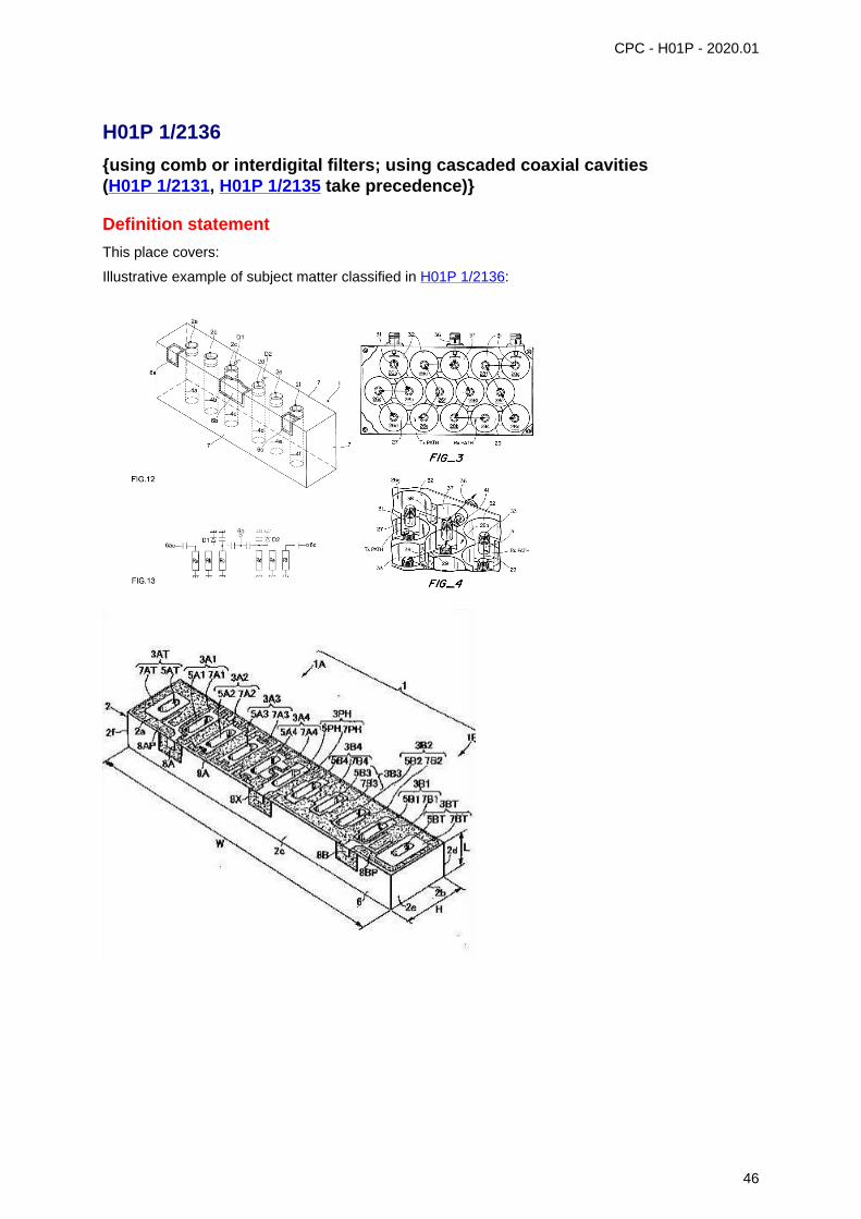
H01P 1/2136
{using comb or interdigital filters; using cascaded coaxial cavities(H01P 1/2131, H01P 1/2135 take precedence)}
Definition statement
This place covers:
Illustrative example of subject matter classified in H01P 1/2136:
46
CPC - H01P - 2020.01
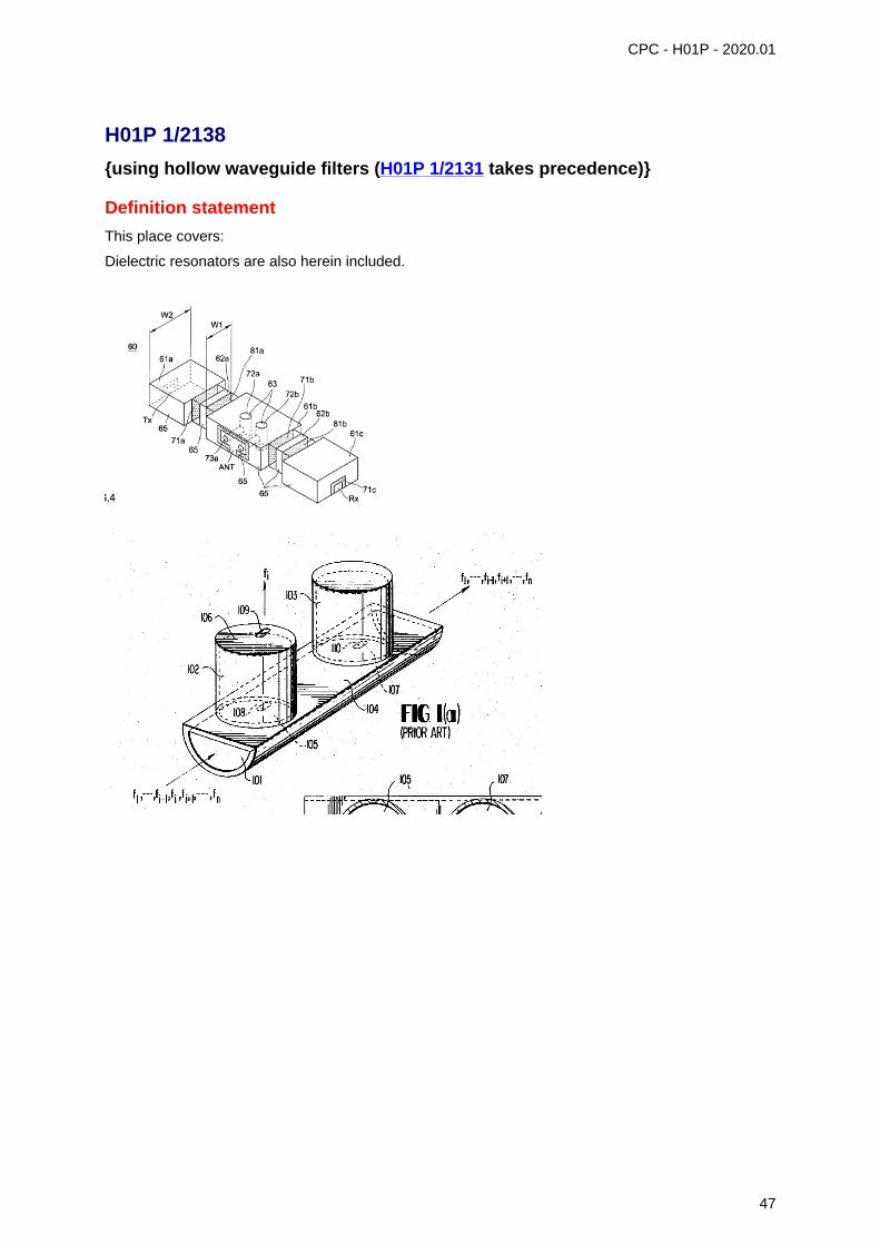
H01P 1/2138
{using hollow waveguide filters (H01P 1/2131 takes precedence)}
Definition statement
This place covers:
Dielectric resonators are also herein included.
47
CPC - H01P - 2020.01
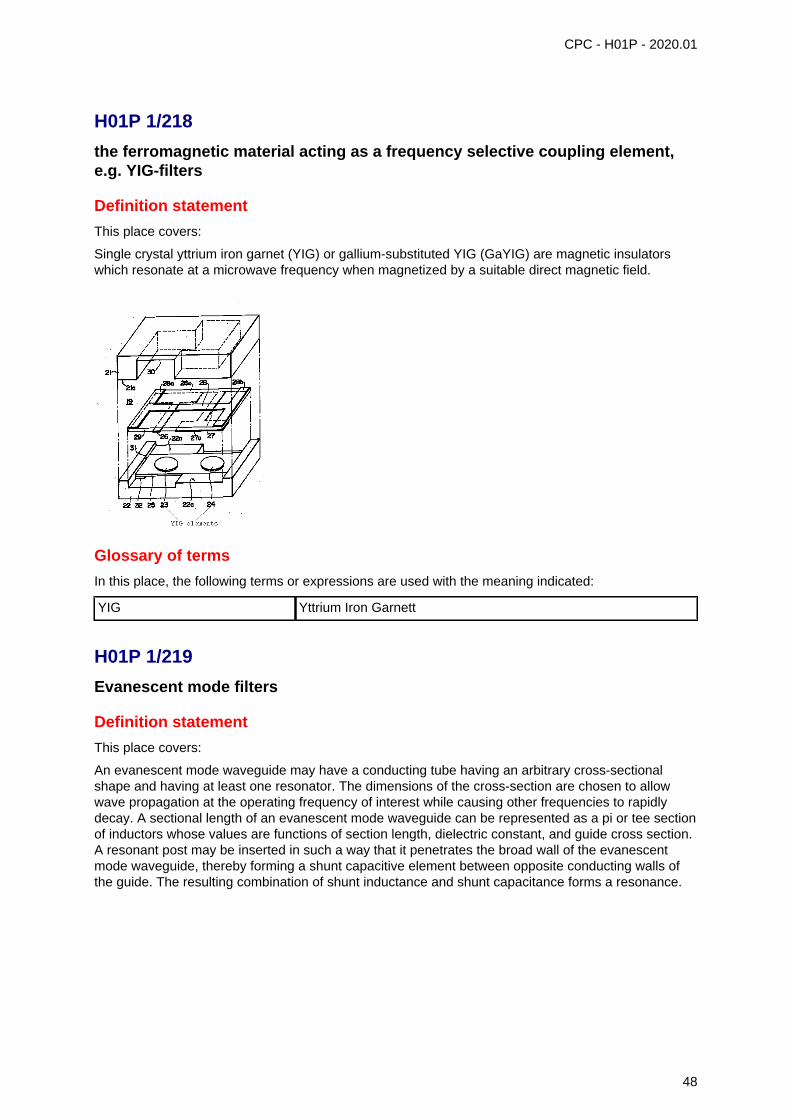
H01P 1/218
the ferromagnetic material acting as a frequency selective coupling element,e.g. YIG-filters
Definition statement
This place covers:
Single crystal yttrium iron garnet (YIG) or gallium-substituted YIG (GaYIG) are magnetic insulatorswhich resonate at a microwave frequency when magnetized by a suitable direct magnetic field.
Glossary of terms
In this place, the following terms or expressions are used with the meaning indicated:
YIG Yttrium Iron Garnett
H01P 1/219
Evanescent mode filters
Definition statement
This place covers:
An evanescent mode waveguide may have a conducting tube having an arbitrary cross-sectionalshape and having at least one resonator. The dimensions of the cross-section are chosen to allowwave propagation at the operating frequency of interest while causing other frequencies to rapidlydecay. A sectional length of an evanescent mode waveguide can be represented as a pi or tee sectionof inductors whose values are functions of section length, dielectric constant, and guide cross section.A resonant post may be inserted in such a way that it penetrates the broad wall of the evanescentmode waveguide, thereby forming a shunt capacitive element between opposite conducting walls ofthe guide. The resulting combination of shunt inductance and shunt capacitance forms a resonance.
48
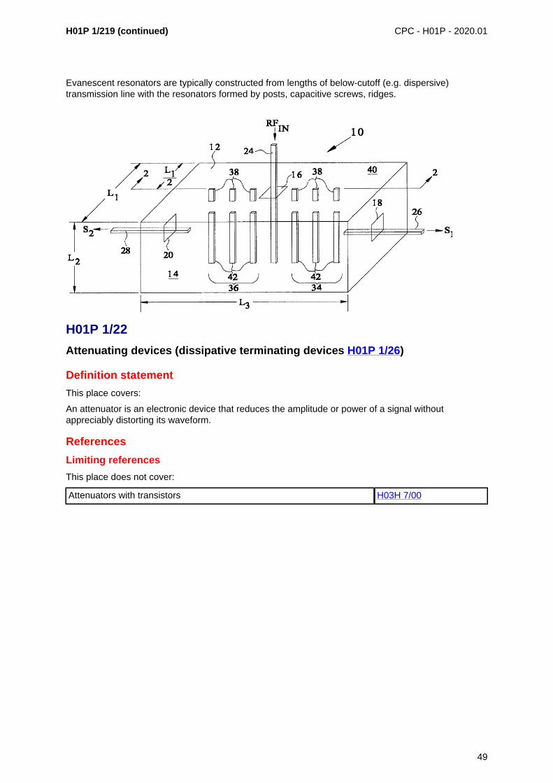
H01P 1/219 (continued) CPC - H01P - 2020.01
Evanescent resonators are typically constructed from lengths of below-cutoff (e.g. dispersive)transmission line with the resonators formed by posts, capacitive screws, ridges.
H01P 1/22
Attenuating devices (dissipative terminating devices H01P 1/26)
Definition statement
This place covers:
An attenuator is an electronic device that reduces the amplitude or power of a signal withoutappreciably distorting its waveform.
References
Limiting references
This place does not cover:
Attenuators with transistors H03H 7/00
49

CPC - H01P - 2020.01
H01P 1/222
{Waveguide attenuators (H01P 1/23 takes precedence)}
Definition statement
This place covers:
Illustrative example of subject matter classified in H01P 1/222:
H01P 1/225
{Coaxial attenuators (H01P 1/23 takes precedence)}
Definition statement
This place covers:
Illustrative example of subject matter classified in H01P 1/225:
50
CPC - H01P - 2020.01
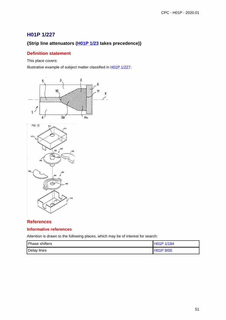
H01P 1/227
{Strip line attenuators (H01P 1/23 takes precedence)}
Definition statement
This place covers:
Illustrative example of subject matter classified in H01P 1/227:
References
Informative references
Attention is drawn to the following places, which may be of interest for search:
Phase shifters H01P 1/184
Delay lines H01P 9/00
51

CPC - H01P - 2020.01
H01P 1/24
Terminating devices
Definition statement
This place covers:
Not only loads
H01P 1/264
{Waveguide terminations (H01P 1/262 takes precedence)}
Definition statement
This place covers:
Illustrative example of subject matter classified in H01P 1/264:
H01P 1/28
Short-circuiting plungers (coupling devices with variable coupling factorH01P 5/04)
Definition statement
This place covers:
Illustrative example of subject matter classified in H01P 1/28:
52
CPC - H01P - 2020.01
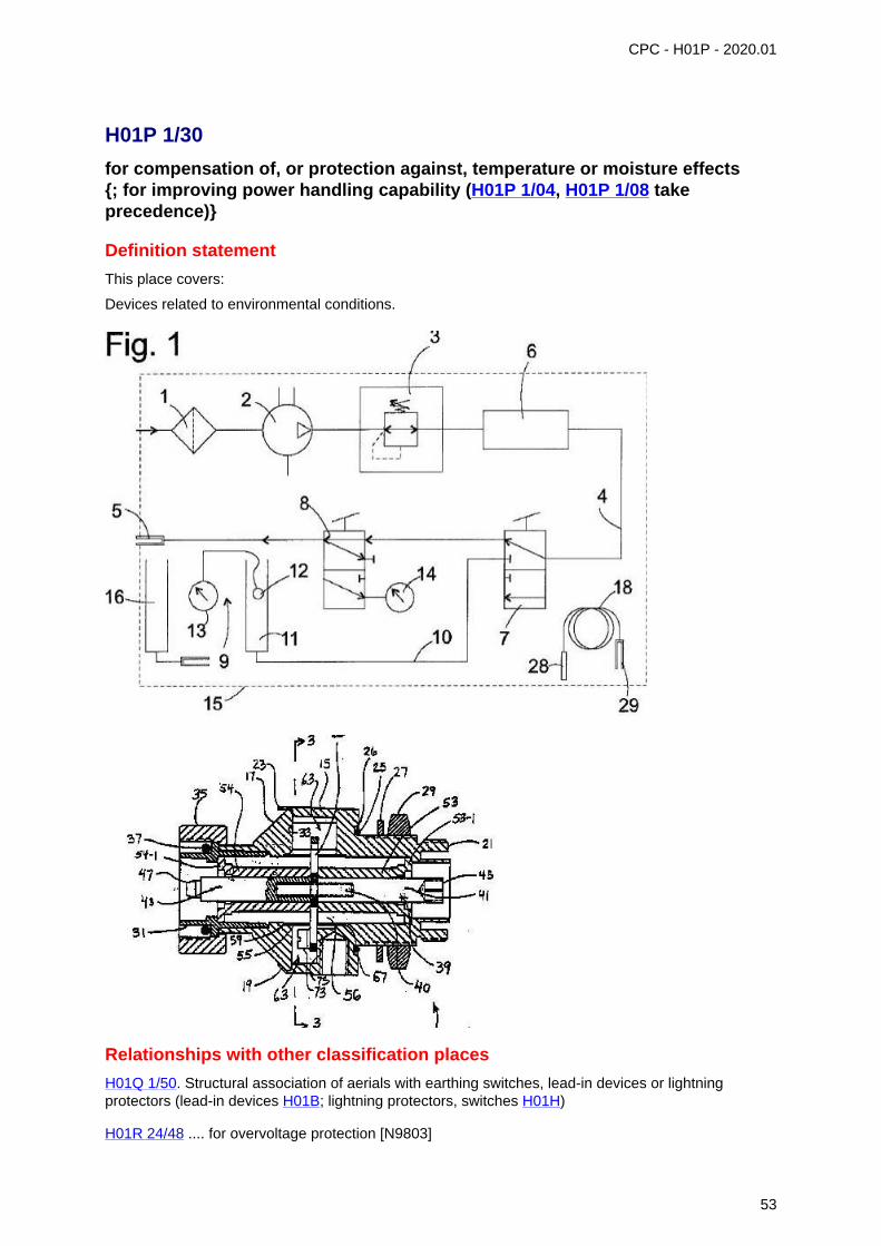
H01P 1/30
for compensation of, or protection against, temperature or moisture effects{; for improving power handling capability (H01P 1/04, H01P 1/08 takeprecedence)}
Definition statement
This place covers:
Devices related to environmental conditions.
Relationships with other classification places
H01Q 1/50. Structural association of aerials with earthing switches, lead-in devices or lightningprotectors (lead-in devices H01B; lightning protectors, switches H01H)
H01R 24/48 .... for overvoltage protection [N9803]
53

H01P 1/30 (continued) CPC - H01P - 2020.01
H01P 1/202... Coaxial filters (cascaded coaxial cavities H01P 1/205)
H01P 1/36
Isolators
Definition statement
This place covers:
An RF isolator is a two-port passive device made of magnets and ferrite material which is used toprotect other RF components from excessive signal reflection.
Usually, one of the ports of the isolator is grounded.
H01P 1/362
{Edge-guided mode devices}
Definition statement
This place covers:
An edge-guided mode device is provided with a dominant mode that resembles TEM energypropagation except that there is a strong transverse field displacement causing the wave energyto be concentrated along the edges of a metal stripline conductor formed on the surface of a ferritesubstrate located on a metal ground plane and having a magnetic field applied thereto perpendicularto the ground plane. The edges are designed to be free of abrupt changes in order that there be
54
H01P 1/362 (continued) CPC - H01P - 2020.01
no abrupt impedance change of the circuit. Non-reciprocal behaviour is obtained by asymmetricallyloading the edges.
See documents US3,617,951 and US3,555,459
H01P 1/365
Resonance absorption isolators
Definition statement
This place covers:
In this class of isolator, an absorption element (dummy load, dielectric member, ferrite slab, etc...)could be coupled to the isolator in order to absorb the energy of a microwave propagating backwardly.
H01P 1/37
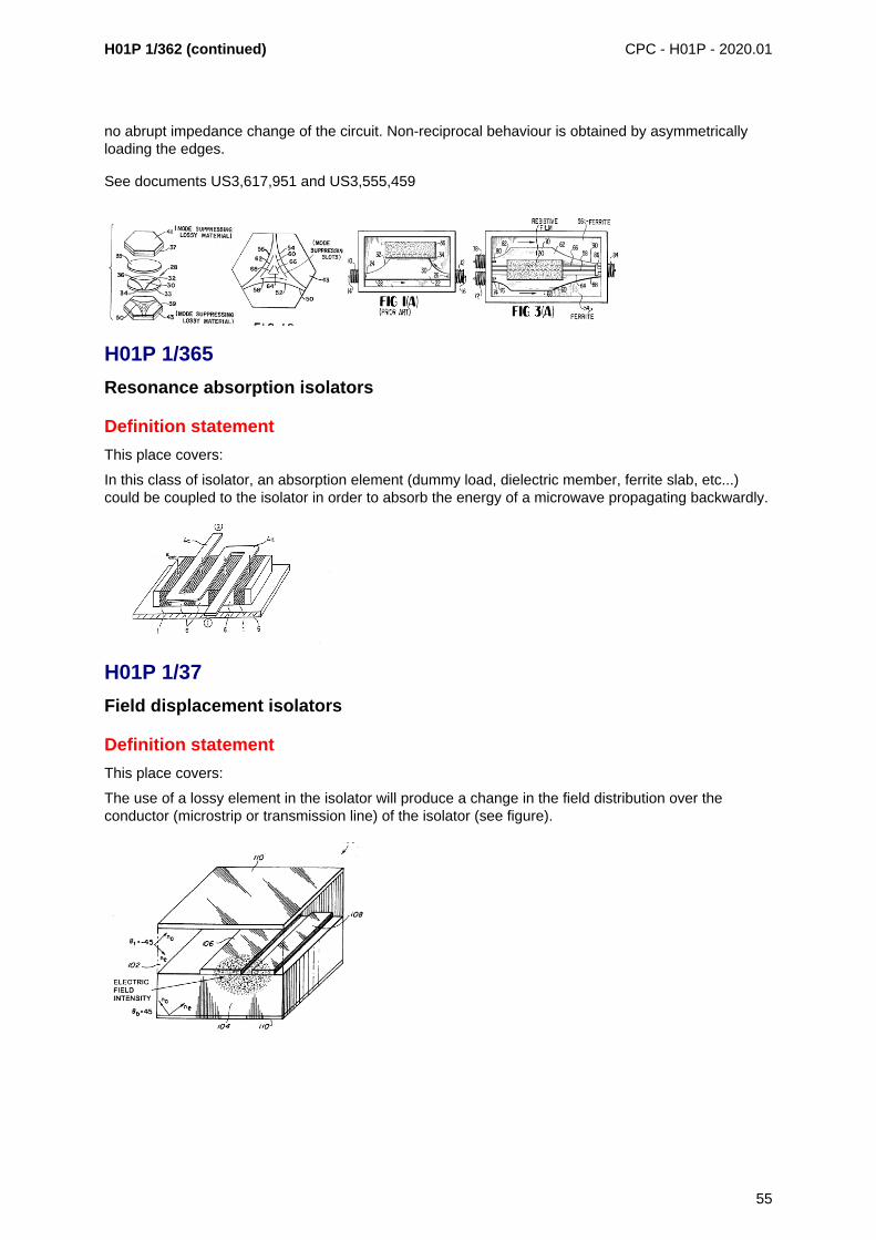
Field displacement isolators
Definition statement
This place covers:
The use of a lossy element in the isolator will produce a change in the field distribution over theconductor (microstrip or transmission line) of the isolator (see figure).
55
CPC - H01P - 2020.01
H01P 1/38
Circulators
Definition statement
This place covers:
Ferrite circulators are typically configured as multi-port (e.g., three-port) passive RF or microwavedevices having within a housing magnets and ferrite material that may be used to control the directionof signal flow in, for example, an RF circuit or a microwave circuit. For example, ferrite circulators maybe used to control signal flow in wireless base station or power amplifier applications. Ferrite isolators(see H01P 1/36) also may be constructed by terminating one port of a ferrite circulator. Terminatingone port results in signal or energy flow in only one direction, which may be used, for example, forisolating components in a chain of interconnected components.
For more general information about circulators/isolators: http://www.tscm.com/circulat.pdf
H01P 1/383
Junction circulators, e.g. Y-circulators
Definition statement
This place covers:
Usually, a 3-port circulator is generally called a Y-junction circulator. In case of specification of thecirculator, see H01P 1/387 (stripline circulators) or H01P 1/39 (waveguide circulators).
H01P 1/387
Strip line circulators
Definition statement
This place covers:
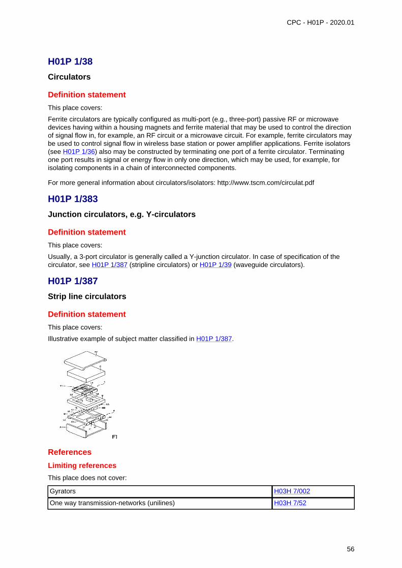
Illustrative example of subject matter classified in H01P 1/387.
References
Limiting references
This place does not cover:
Gyrators H03H 7/002
One way transmission-networks (unilines) H03H 7/52
56
CPC - H01P - 2020.01
H01P 1/39
Hollow waveguide circulators
Definition statement
This place covers:
Illustrative example of subject matter classified in H01P 1/39:
H01P 1/393
using Faraday rotators
Definition statement
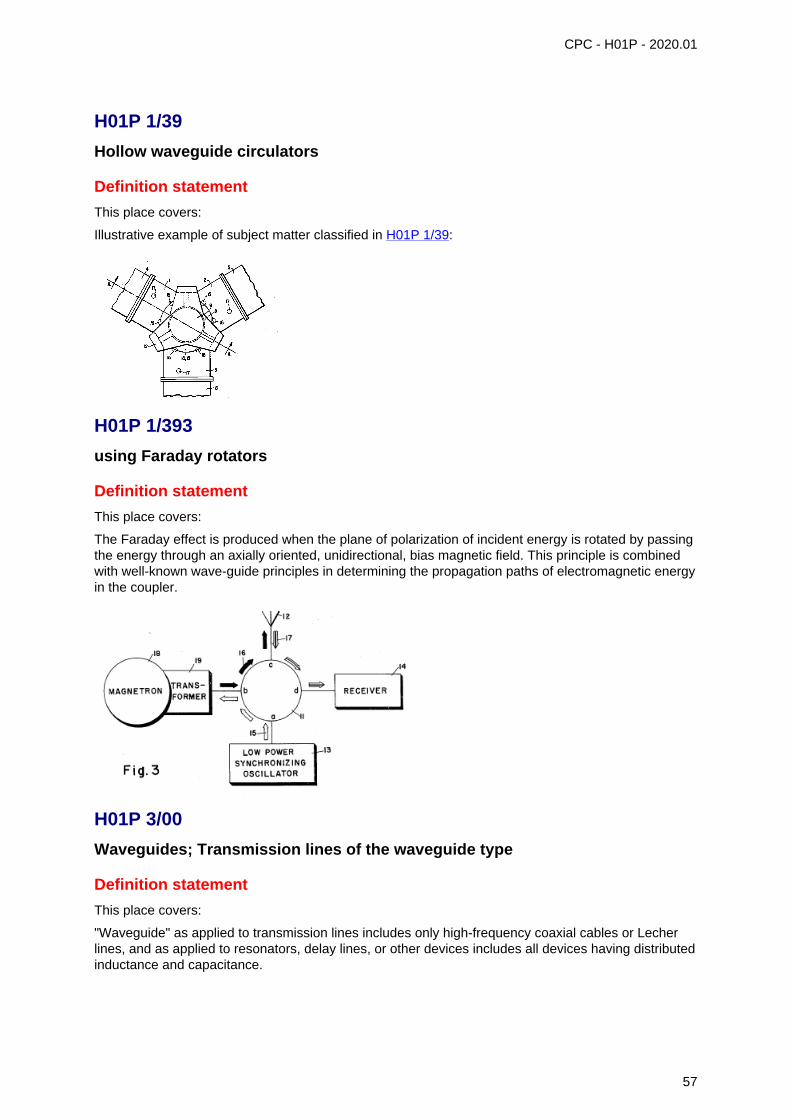
This place covers:
The Faraday effect is produced when the plane of polarization of incident energy is rotated by passingthe energy through an axially oriented, unidirectional, bias magnetic field. This principle is combinedwith well-known wave-guide principles in determining the propagation paths of electromagnetic energyin the coupler.
H01P 3/00
Waveguides; Transmission lines of the waveguide type
Definition statement
This place covers:
"Waveguide" as applied to transmission lines includes only high-frequency coaxial cables or Lecherlines, and as applied to resonators, delay lines, or other devices includes all devices having distributedinductance and capacitance.
57
CPC - H01P - 2020.01
H01P 3/003
{Coplanar lines}
Definition statement
This place covers:
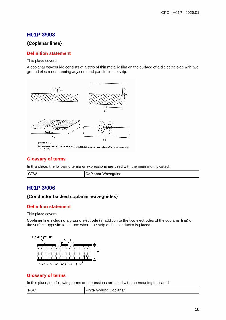
A coplanar waveguide consists of a strip of thin metallic film on the surface of a dielectric slab with twoground electrodes running adjacent and parallel to the strip.
Glossary of terms
In this place, the following terms or expressions are used with the meaning indicated:
CPW CoPlanar Waveguide
H01P 3/006
{Conductor backed coplanar waveguides}
Definition statement
This place covers:
Coplanar line including a ground electrode (in addition to the two electrodes of the coplanar line) onthe surface opposite to the one where the strip of thin conductor is placed.
Glossary of terms
In this place, the following terms or expressions are used with the meaning indicated:
FGC Finite Ground Coplanar
58

H01P 3/006 (continued) CPC - H01P - 2020.01
CBCPW Conductor Backed Coplanar Waveguide
H01P 3/023
{Fin lines; Slot lines}
Definition statement
This place covers:
A fin-line is a shielded slot line.
Slot line
Fin-line
59
CPC - H01P - 2020.01
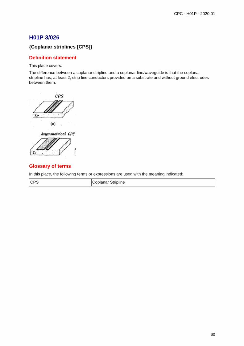
H01P 3/026
{Coplanar striplines [CPS]}
Definition statement
This place covers:
The difference between a coplanar stripline and a coplanar line/waveguide is that the coplanarstripline has, at least 2, strip line conductors provided on a substrate and without ground electrodesbetween them.
Glossary of terms
In this place, the following terms or expressions are used with the meaning indicated:
CPS Coplanar Stripline
60
CPC - H01P - 2020.01
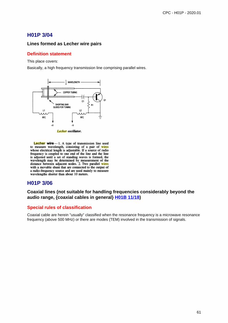
H01P 3/04
Lines formed as Lecher wire pairs
Definition statement
This place covers:
Basically, a high frequency transmission line comprising parallel wires.
H01P 3/06
Coaxial lines (not suitable for handling frequencies considerably beyond theaudio range, {coaxial cables in general} H01B 11/18)
Special rules of classification
Coaxial cable are herein "usually" classified when the resonance frequency is a microwave resonancefrequency (above 500 MHz) or there are modes (TEM) involved in the transmission of signals.
61
CPC - H01P - 2020.01
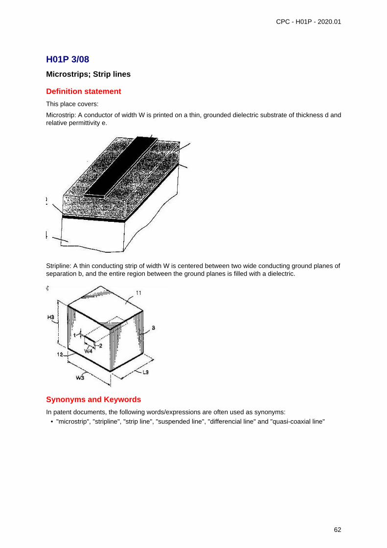
H01P 3/08
Microstrips; Strip lines
Definition statement
This place covers:
Microstrip: A conductor of width W is printed on a thin, grounded dielectric substrate of thickness d andrelative permittivity e.
Stripline: A thin conducting strip of width W is centered between two wide conducting ground planes ofseparation b, and the entire region between the ground planes is filled with a dielectric.
Synonyms and Keywords
In patent documents, the following words/expressions are often used as synonyms:
• "microstrip", "stripline", "strip line", "suspended line", "differencial line" and "quasi-coaxial line"
62
CPC - H01P - 2020.01
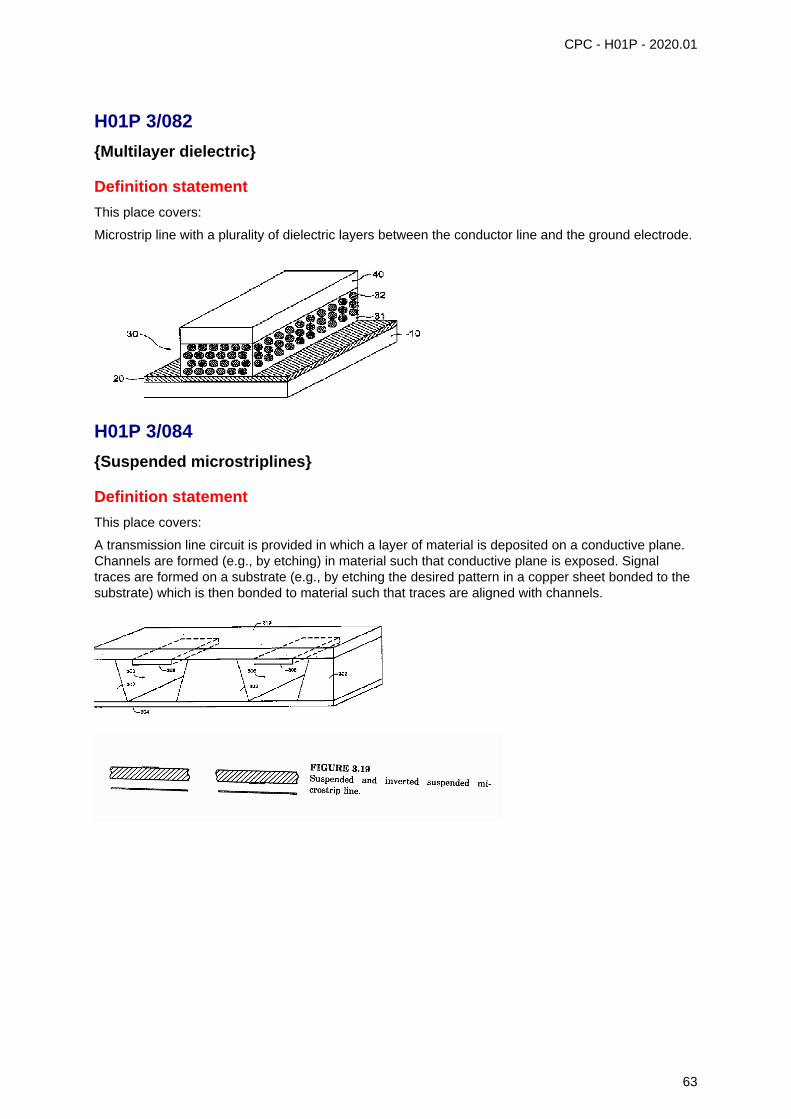
H01P 3/082
{Multilayer dielectric}
Definition statement
This place covers:
Microstrip line with a plurality of dielectric layers between the conductor line and the ground electrode.
H01P 3/084
{Suspended microstriplines}
Definition statement
This place covers:
A transmission line circuit is provided in which a layer of material is deposited on a conductive plane.Channels are formed (e.g., by etching) in material such that conductive plane is exposed. Signaltraces are formed on a substrate (e.g., by etching the desired pattern in a copper sheet bonded to thesubstrate) which is then bonded to material such that traces are aligned with channels.
63
CPC - H01P - 2020.01
H01P 3/085
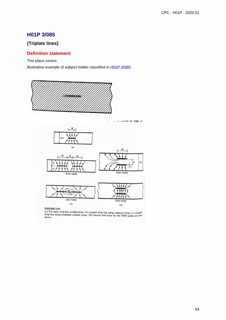
{Triplate lines}
Definition statement
This place covers:
Illustrative example of subject matter classified in H01P 3/085:
64
CPC - H01P - 2020.01
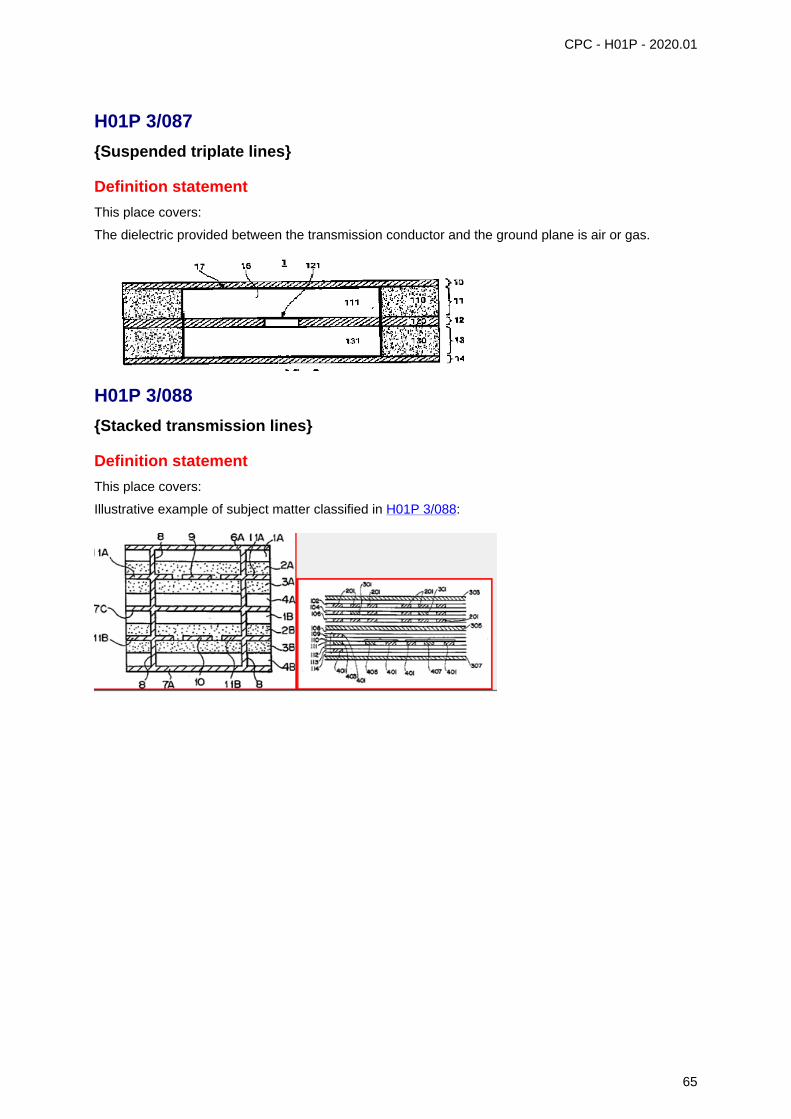
H01P 3/087
{Suspended triplate lines}
Definition statement
This place covers:
The dielectric provided between the transmission conductor and the ground plane is air or gas.
H01P 3/088
{Stacked transmission lines}
Definition statement
This place covers:
Illustrative example of subject matter classified in H01P 3/088:
65
CPC - H01P - 2020.01
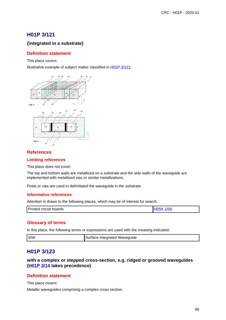
H01P 3/121
{integrated in a substrate}
Definition statement
This place covers:
Illustrative example of subject matter classified in H01P 3/121:
References
Limiting references
This place does not cover:
The top and bottom walls are metallized on a substrate and the side walls of the waveguide areimplemented with metallized vias or similar metallizations.
Posts or vias are used to delimitated the waveguide in the substrate.
Informative references
Attention is drawn to the following places, which may be of interest for search:
Printed circuit boards H05K 1/00
Glossary of terms
In this place, the following terms or expressions are used with the meaning indicated:
SIW Surface Integrated Waveguide
H01P 3/123
with a complex or stepped cross-section, e.g. ridged or grooved waveguides(H01P 3/14 takes precedence)
Definition statement
This place covers:
Metallic waveguides comprising a complex cross section.
66
H01P 3/123 (continued) CPC - H01P - 2020.01
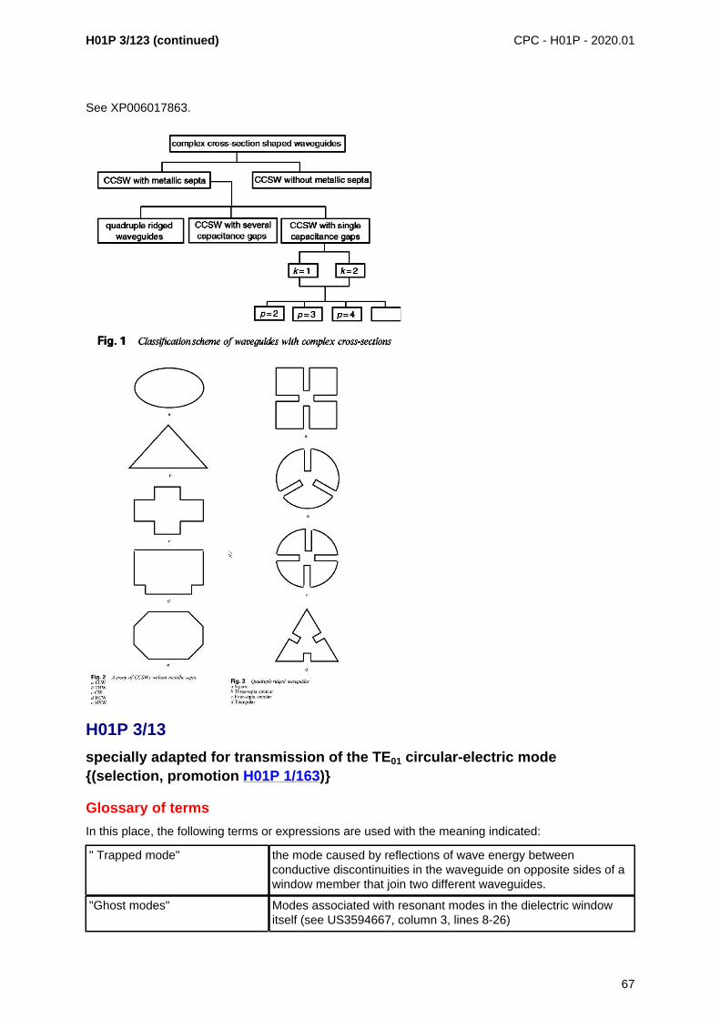
See XP006017863.
H01P 3/13
specially adapted for transmission of the TE01 circular-electric mode{(selection, promotion H01P 1/163)}
Glossary of terms
In this place, the following terms or expressions are used with the meaning indicated:
" Trapped mode" the mode caused by reflections of wave energy betweenconductive discontinuities in the waveguide on opposite sides of awindow member that join two different waveguides.
"Ghost modes" Modes associated with resonant modes in the dielectric windowitself (see US3594667, column 3, lines 8-26)
67
CPC - H01P - 2020.01
H01P 3/16
Dielectric waveguides, i.e. without a longitudinal conductor
Definition statement
This place covers:
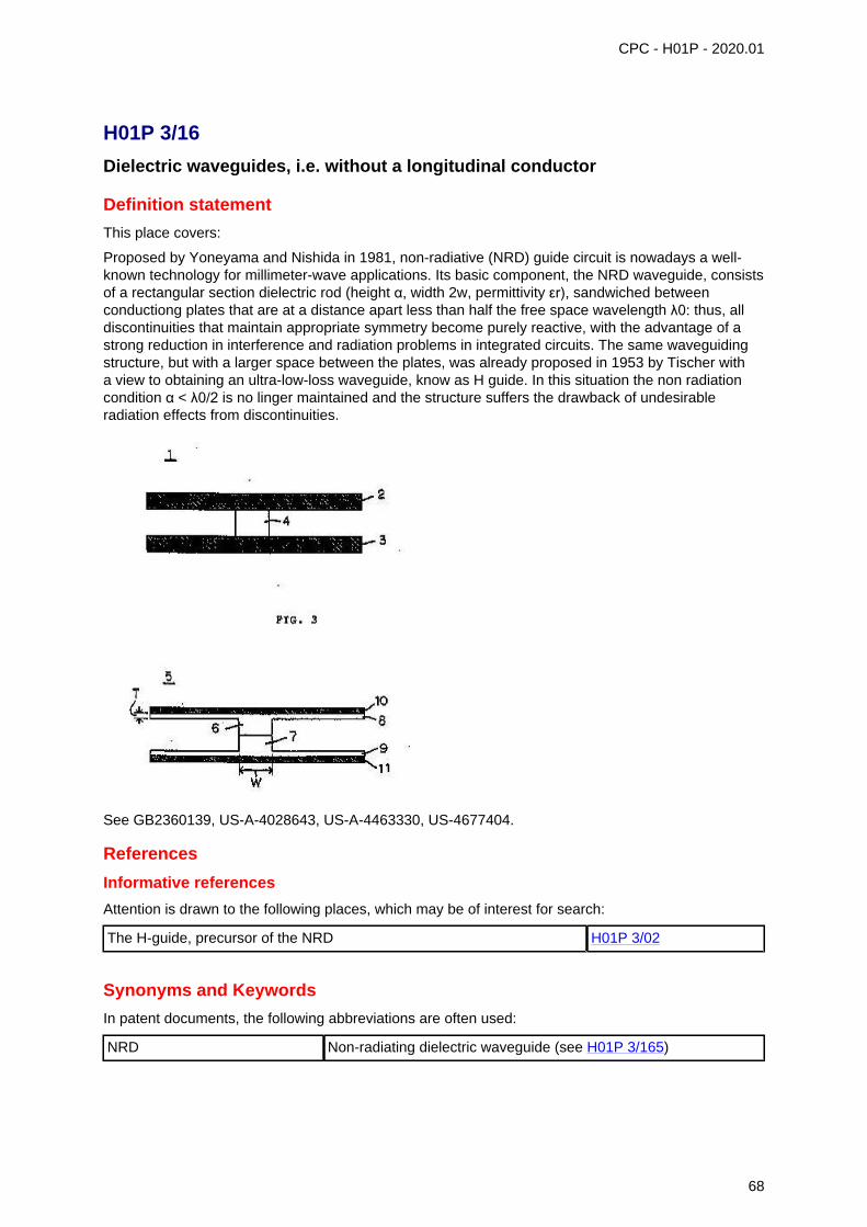
Proposed by Yoneyama and Nishida in 1981, non-radiative (NRD) guide circuit is nowadays a well-known technology for millimeter-wave applications. Its basic component, the NRD waveguide, consistsof a rectangular section dielectric rod (height α, width 2w, permittivity εr), sandwiched betweenconductiong plates that are at a distance apart less than half the free space wavelength λ0: thus, alldiscontinuities that maintain appropriate symmetry become purely reactive, with the advantage of astrong reduction in interference and radiation problems in integrated circuits. The same waveguidingstructure, but with a larger space between the plates, was already proposed in 1953 by Tischer witha view to obtaining an ultra-low-loss waveguide, know as H guide. In this situation the non radiationcondition α < λ0/2 is no linger maintained and the structure suffers the drawback of undesirableradiation effects from discontinuities.
See GB2360139, US-A-4028643, US-A-4463330, US-4677404.
References
Informative references
Attention is drawn to the following places, which may be of interest for search:
The H-guide, precursor of the NRD H01P 3/02
Synonyms and Keywords
In patent documents, the following abbreviations are often used:
NRD Non-radiating dielectric waveguide (see H01P 3/165)
68
CPC - H01P - 2020.01
H01P 3/165
{Non-radiating dielectric waveguides}
Definition statement
This place covers:
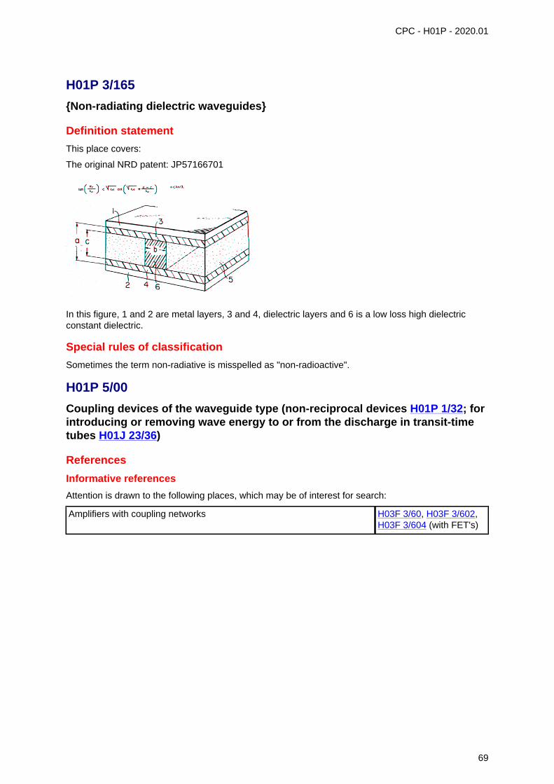
The original NRD patent: JP57166701
In this figure, 1 and 2 are metal layers, 3 and 4, dielectric layers and 6 is a low loss high dielectricconstant dielectric.
Special rules of classification
Sometimes the term non-radiative is misspelled as "non-radioactive".
H01P 5/00
Coupling devices of the waveguide type (non-reciprocal devices H01P 1/32; forintroducing or removing wave energy to or from the discharge in transit-timetubes H01J 23/36)
References
Informative references
Attention is drawn to the following places, which may be of interest for search:
Amplifiers with coupling networks H03F 3/60, H03F 3/602,H03F 3/604 (with FET's)
69
CPC - H01P - 2020.01
H01P 5/04
with variable factor of coupling
Definition statement
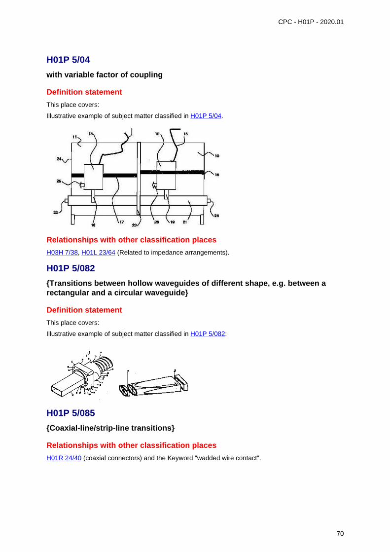
This place covers:
Illustrative example of subject matter classified in H01P 5/04.
Relationships with other classification places
H03H 7/38, H01L 23/64 (Related to impedance arrangements).
H01P 5/082
{Transitions between hollow waveguides of different shape, e.g. between arectangular and a circular waveguide}
Definition statement
This place covers:
Illustrative example of subject matter classified in H01P 5/082:
H01P 5/085
{Coaxial-line/strip-line transitions}
Relationships with other classification places
H01R 24/40 (coaxial connectors) and the Keyword "wadded wire contact".
70
CPC - H01P - 2020.01
H01P 5/10
for coupling balanced with unbalanced lines or devices
Definition statement
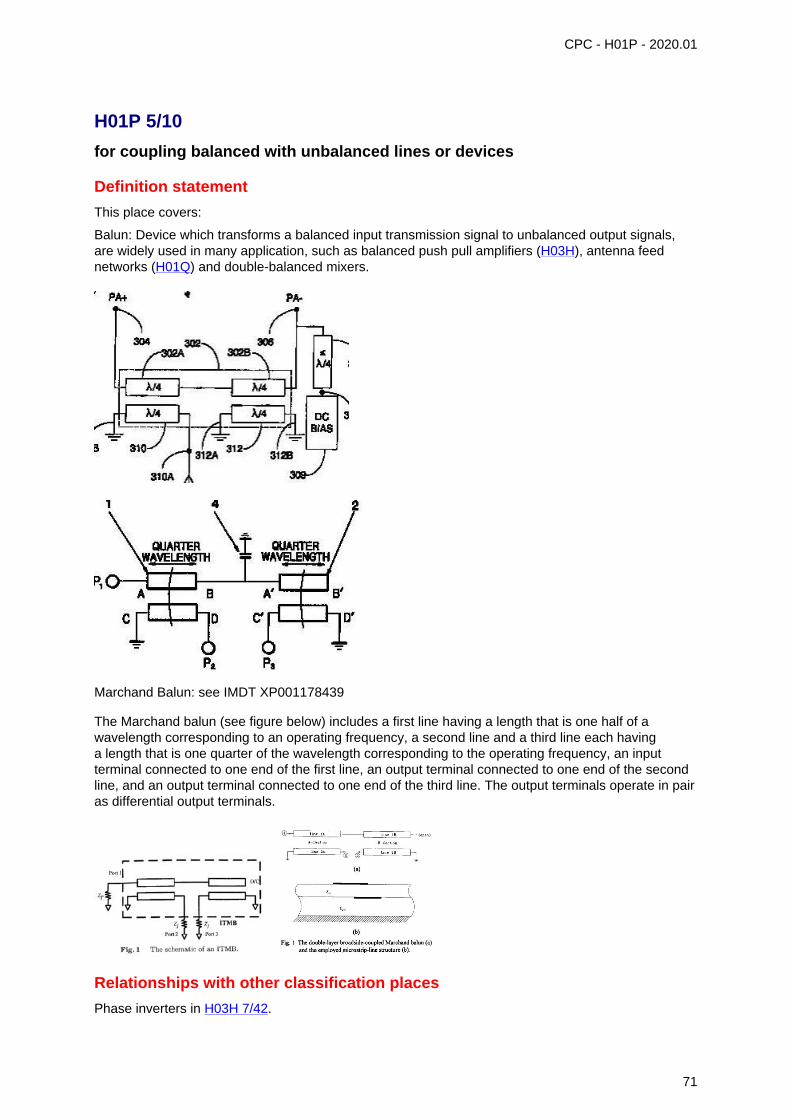
This place covers:
Balun: Device which transforms a balanced input transmission signal to unbalanced output signals,are widely used in many application, such as balanced push pull amplifiers (H03H), antenna feednetworks (H01Q) and double-balanced mixers.
Marchand Balun: see IMDT XP001178439
The Marchand balun (see figure below) includes a first line having a length that is one half of awavelength corresponding to an operating frequency, a second line and a third line each havinga length that is one quarter of the wavelength corresponding to the operating frequency, an inputterminal connected to one end of the first line, an output terminal connected to one end of the secondline, and an output terminal connected to one end of the third line. The output terminals operate in pairas differential output terminals.
Relationships with other classification places
Phase inverters in H03H 7/42.
71

H01P 5/10 (continued) CPC - H01P - 2020.01
Glossary of terms
In this place, the following terms or expressions are used with the meaning indicated:
Balun, symetriseur Balance-Unbalanced coupling device
H01P 5/107
Hollow-waveguide/strip-line transitions
Definition statement
This place covers:
SMT (surface mount technology)
Relationships with other classification places
H01P 7/065: when it is referring to a waveguide cavity in the PCB.
Look also in:
H01P 1/161: sustaining two independent orthogonal modes, e.g. orthomode transducer (combining orseparating polarisations and frequencies H01P 1/2131)
H01P 1/17: for producing a continuously rotating polarisation, e.g. circular polarisation
72

CPC - H01P - 2020.01
H01P 5/16
Conjugate devices, i.e. devices having at least one port decoupled from oneother port
Definition statement
This place covers:
Reference document: E. Wilkinson: "An N-way Hybrid Power divider", IEEE Trans., vol. MTT-8, pp116-118
Relationships with other classification places
H03H 7/185 Multiple networks...comprising distributed impedance elements together with lumpedimpedance elements.
Glossary of terms
In this place, the following terms or expressions are used with the meaning indicated:
Wilkinson power divider N-way power divider that splits the input power into output powerat N ports and that also provides isolationbetween the outputpowers.
H01P 5/18
consisting of two coupled guides, e.g. directional couplers
Definition statement
This place covers:
Directional couplers are four-port circuits where one port is isolated from the input port. All four portsare (ideally) matched, and the circuit is (ideally) lossless.
What do we mean by "directional"? A directional coupler has four ports, where one is regarded as theinput, one is regarded as the "through" port (where most of the incident signal exits), one is regardedas the coupled port (where a fixed fraction of the input signal appears, usually expressed in dB), andan isolated port, which is usually terminated. If the signal is reversed so that it enter the "though" port,most of it exits the "input" port, but the coupled port is now the port that was previously regarded asthe "isolated port". The coupled port is a function of which port is the incident port.
73
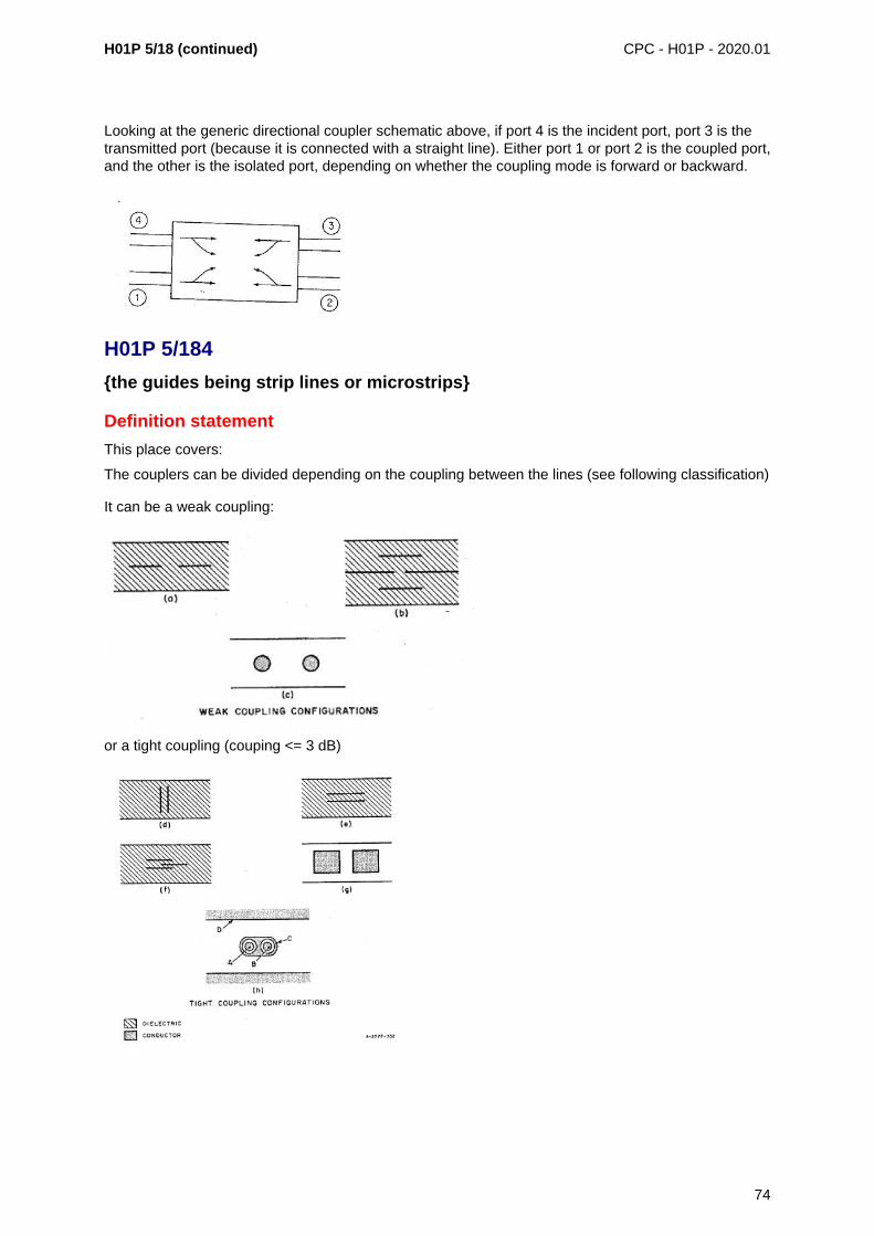
H01P 5/18 (continued) CPC - H01P - 2020.01
Looking at the generic directional coupler schematic above, if port 4 is the incident port, port 3 is thetransmitted port (because it is connected with a straight line). Either port 1 or port 2 is the coupled port,and the other is the isolated port, depending on whether the coupling mode is forward or backward.
H01P 5/184
{the guides being strip lines or microstrips}
Definition statement
This place covers:
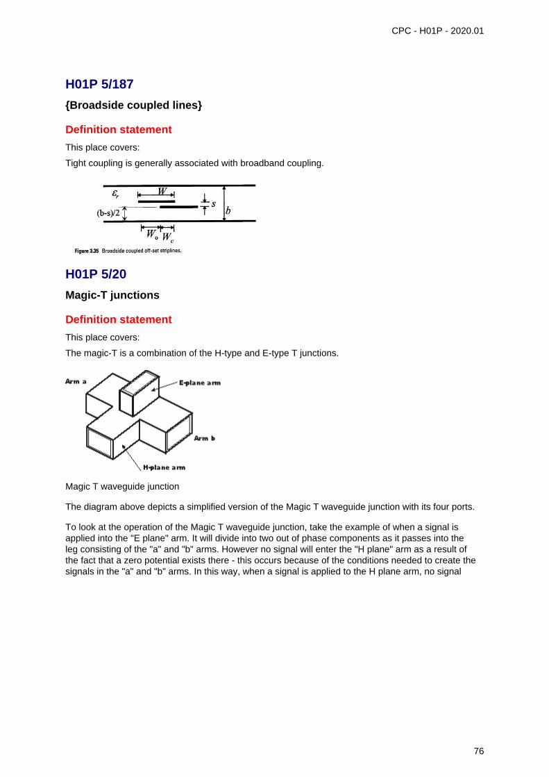
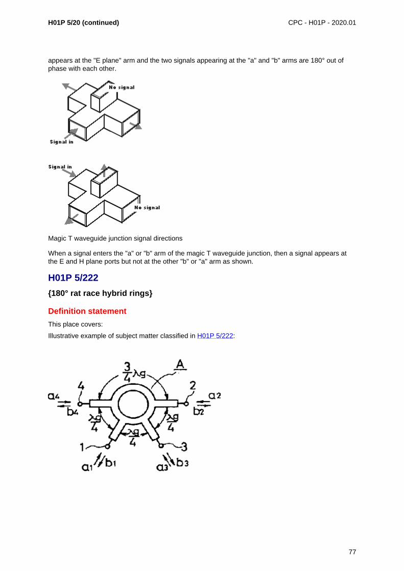
The couplers can be divided depending on the coupling between the lines (see following classification)
It can be a weak coupling:
or a tight coupling (couping <= 3 dB)
74

CPC - H01P - 2020.01
H01P 5/185
{Edge coupled lines}
Definition statement
This place covers:
Weak coupling is associated with edge coupling (except Lange couplers (see H01P 5/186)).
H01P 5/186
{Lange couplers}
Definition statement
This place covers:
Lange couplers are generally used to couple electromagnetic energy between transmission lines. In afour port hybrid, there is an input port and a direct port, these two ports being directly and conductivelyconnected to each other, as well as a coupled port, the latter being connected to transmission linescoupled electromagnetically (inductively and capacitively) to the conductors extending between theinput and direct ports.
In a Lange type coupler, each strip conductor is divided into mutually parallel sections, and theconductor sections from the two different strip conductors are interdigitated, so that each strip sectionis located between two sections from the other conductor. In a planar arrangement, it is necessary tohave cross-over connectors in order to establish a direct conductive connection between the varioussections extending in parallel.
75
CPC - H01P - 2020.01
H01P 5/187
{Broadside coupled lines}
Definition statement
This place covers:
Tight coupling is generally associated with broadband coupling.
H01P 5/20
Magic-T junctions
Definition statement
This place covers:
The magic-T is a combination of the H-type and E-type T junctions.
Magic T waveguide junction
The diagram above depicts a simplified version of the Magic T waveguide junction with its four ports.
To look at the operation of the Magic T waveguide junction, take the example of when a signal isapplied into the "E plane" arm. It will divide into two out of phase components as it passes into theleg consisting of the "a" and "b" arms. However no signal will enter the "H plane" arm as a result ofthe fact that a zero potential exists there - this occurs because of the conditions needed to create thesignals in the "a" and "b" arms. In this way, when a signal is applied to the H plane arm, no signal
76
H01P 5/20 (continued) CPC - H01P - 2020.01
appears at the "E plane" arm and the two signals appearing at the "a" and "b" arms are 180° out ofphase with each other.
Magic T waveguide junction signal directions
When a signal enters the "a" or "b" arm of the magic T waveguide junction, then a signal appears atthe E and H plane ports but not at the other "b" or "a" arm as shown.
H01P 5/222
{180° rat race hybrid rings}
Definition statement
This place covers:
Illustrative example of subject matter classified in H01P 5/222:
77
CPC - H01P - 2020.01
H01P 5/225
{180° reversed phase hybrid rings}
Definition statement
This place covers:
See US4023123.
H01P 5/227
{90° branch line couplers}
Definition statement
This place covers:
Illustrative example of subject matter classified in H01P 5/227:
78
CPC - H01P - 2020.01
H01P 7/00
Resonators of the waveguide type ({variable impedance transformersH01P 5/04}; structurally associated with transit-time tubes and interactingwith the discharge therein H01J 23/18; {generators of electronic oscillationsusing resonators of this type H03B 5/18, H03B 7/14, H03B 9/14; electronicamplifiers using resonators of this type H03F 3/54}; microwave heating devicesH05B 6/64)
References
Informative references
Attention is drawn to the following places, which may be of interest for search:
Construction of impedance networks... H03H 1/00
One port networks comprising passive electrical elements... H03H 5/00
Multiple port networks with passive electrical elements... H03H 7/00
H01P 7/06
Cavity resonators
References
Informative references
Attention is drawn to the following places, which may be of interest for search:
Cavity resonators H01J 23/20
H01P 7/065
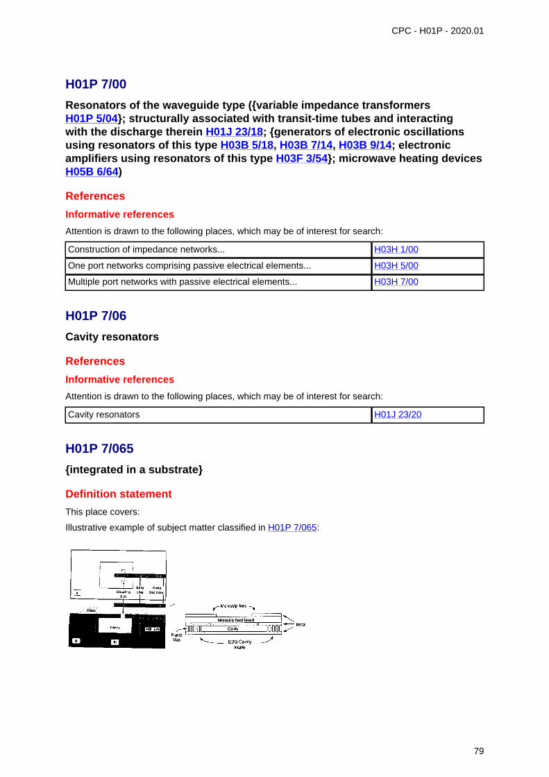
{integrated in a substrate}
Definition statement
This place covers:
Illustrative example of subject matter classified in H01P 7/065:
79
CPC - H01P - 2020.01
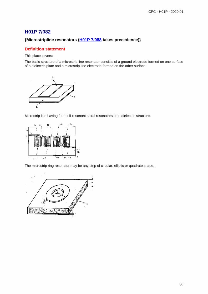
H01P 7/082
{Microstripline resonators (H01P 7/088 takes precedence)}
Definition statement
This place covers:
The basic structure of a microstrip line resonator consists of a ground electrode formed on one surfaceof a dielectric plate and a microstrip line electrode formed on the other surface.
Microstrip line having four self-resonant spiral resonators on a dielectric structure.
The microstrip ring resonator may be any strip of circular, elliptic or quadrate shape.
80
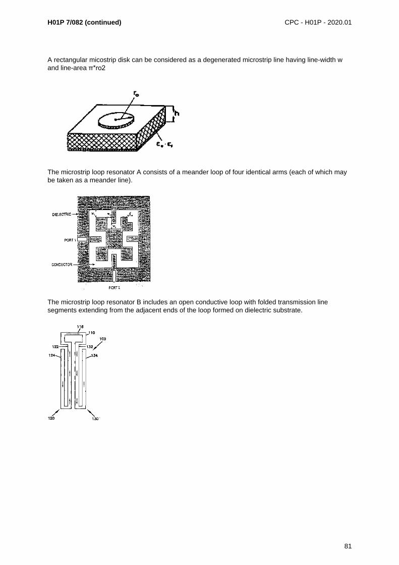
H01P 7/082 (continued) CPC - H01P - 2020.01
A rectangular micostrip disk can be considered as a degenerated microstrip line having line-width wand line-area π*ro2
The microstrip loop resonator A consists of a meander loop of four identical arms (each of which maybe taken as a meander line).
The microstrip loop resonator B includes an open conductive loop with folded transmission linesegments extending from the adjacent ends of the loop formed on dielectric substrate.
81
H01P 7/082 (continued) CPC - H01P - 2020.01
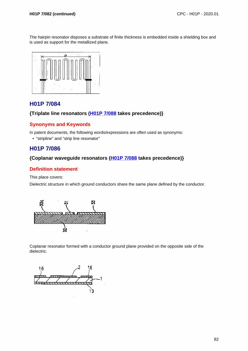
The hairpin resonator disposes a substrate of finite thickness is embedded inside a shielding box andis used as support for the metallized plane.
H01P 7/084
{Triplate line resonators (H01P 7/088 takes precedence)}
Synonyms and Keywords
In patent documents, the following words/expressions are often used as synonyms:
• "stripline" and "strip line resonator"
H01P 7/086
{Coplanar waveguide resonators (H01P 7/088 takes precedence)}
Definition statement
This place covers:
Dielectric structure in which ground conductors share the same plane defined by the conductor.
Coplanar resonator formed with a conductor ground plane provided on the opposite side of thedielectric.
82
CPC - H01P - 2020.01
H01P 7/088
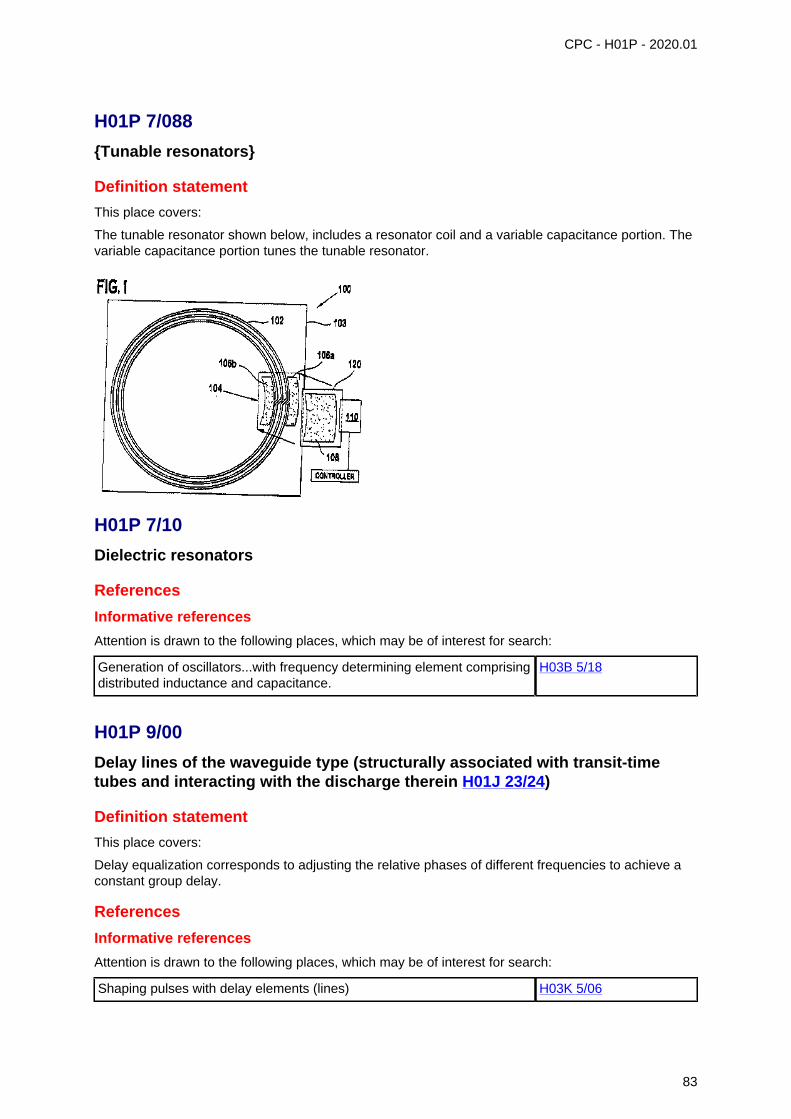
{Tunable resonators}
Definition statement
This place covers:
The tunable resonator shown below, includes a resonator coil and a variable capacitance portion. Thevariable capacitance portion tunes the tunable resonator.
H01P 7/10
Dielectric resonators
References
Informative references
Attention is drawn to the following places, which may be of interest for search:
Generation of oscillators...with frequency determining element comprisingdistributed inductance and capacitance.
H03B 5/18
H01P 9/00
Delay lines of the waveguide type (structurally associated with transit-timetubes and interacting with the discharge therein H01J 23/24)
Definition statement
This place covers:
Delay equalization corresponds to adjusting the relative phases of different frequencies to achieve aconstant group delay.
References
Informative references
Attention is drawn to the following places, which may be of interest for search:
Shaping pulses with delay elements (lines) H03K 5/06
83
CPC - H01P - 2020.01
H01P 11/00
Apparatus or processes specially adapted for manufacturing waveguidesor resonators, lines, or other devices of the waveguide type (manufacture ofcoaxial cables H01B 13/00)
References
Informative references
Attention is drawn to the following places, which may be of interest for search:
Manufacture of coaxial cable H01B 13/00
Manufacturing of antennas H01Q 15/141and subgroups,H01Q 13/0283,H01Q 21/0087
H01P 11/001
{Manufacturing waveguides or transmission lines of the waveguide type}
References
Informative references
Attention is drawn to the following places, which may be of interest for search:
Optical waveguides G02B 6/10
H01P 11/002
{Manufacturing hollow waveguides}
References
Informative references
Attention is drawn to the following places, which may be of interest for search:
Manufacturing tubes B21C 37/15 andsubgroups
H01P 11/003
{Manufacturing lines with conductors on a substrate, e.g. strip lines, slot lines}
Synonyms and Keywords
In patent documents, the following words/expressions are often used as synonyms:
• "etching", "manufacturing", " deposition" and "sputtering"
84