Waveform Generator Module - xDevs.com · The WAVl Waveform Generator Module provides one channel of...
33
WAVI Waveform Generator Module Introduction The WAVl Waveform Generator Module provides one channel of sine, square or triangle waveform output. The module is comparable to a standard function generator in which the adjustment knobs and switches have been re- placed by programmable D/A converters and software switches. The main WAVl functions of frequency, duty cycle <symmetry), amplitude and DC offset are program- mable to 1 part in 4096 ( 12-bit resolution). Output voltage range is switch-selectable at 1V or 1OV. The WAVl’s output waveform is available on a standard BNC connector. The main output as well as T&level trigger outputs are also available from an on-board screw terminal block. Available frequencies cover O.lHz to 2OOKHz in six dec- ade-weighted ranges. Accuracy is typically 5% of setting (10% on Wz and 20Hz ranges). For optimum accuracy, the WAVl should be operated in the upper 90% of any given frequency range. Amplitude accuracy is 5% (to 20V P-I? into 500 ohms). Peak output current is 2OmA. The WAVl duty cycle is programmable from 5% to 95%. Sine wave distortion is typically less than 3%. The WAVl includes a selectable synchronous stop feature. Synchronous stop allows the waveform output to com- plete the current output cycle, even though the WAVl output may have been disabled before this point. Alter- nately, the WAVl output can be set up to return to 0 immediately when the output is disabled. A waveform always starts at the lowest amplitude point of the triangle and sine waves. DC output and offset function may be used to bias output waveforms. Alternately, the WAVl may be used as a general-purpose bipolar bias source of flOV at 2OmA.The WAVl can also be used to pace the conversion rate of the AMMlA or AMM.2 modules at rates other than those provided by the AMM module crystal oscillator. Hardware Compatibility TheWAVlcanbeoperatedinslots2through10ofthe500A or 5OOP mainframe, or in the option slot of the Model 570 or 575. If the WAVl will be used to control an AMM module via its trigger input, the AMM module must have PAL revision D or later. If an AMMlA or AMM2 is not resident in the system, resistor R53 must be installed on the WAVl to supply a system reference voltage. Software Compatibility All WAVl functions can be accessed by writing control information directly to the WAVl’s slot-dependent Com- mand A (CMDA) and Command B (CMDB) registers. These functions include frequency, duty cycle, range, function, amplitude, offset, synchronous stop enable/dis- able, and global strobe enable/disable. Control can also be exercised through any high- or low- level language which permits writes to memory addresses (e.g. BASIC POKES). The WAVl registers are write-only. See the WAVl register map information later in this manual. If you are using third-party software, be certain that the software is compatible with the WAVl. Document Number: 501-921-01 Rev. A / 7-90 CopyrightQ 1990 KeithIey Instruments, Inc. Cleveland, OH 44139 (216)248-0400 WAVI-1
Transcript of Waveform Generator Module - xDevs.com · The WAVl Waveform Generator Module provides one channel of...
WAVI Waveform Generator Module
Introduction
The WAVl Waveform Generator Module provides one channel of sine, square or triangle waveform output. The module is comparable to a standard function generator in which the adjustment knobs and switches have been re- placed by programmable D/A converters and software switches. The main WAVl functions of frequency, duty cycle <symmetry), amplitude and DC offset are program- mable to 1 part in 4096 ( 12-bit resolution). Output voltage range is switch-selectable at 1V or 1OV.
The WAVl’s output waveform is available on a standard BNC connector. The main output as well as T&level trigger outputs are also available from an on-board screw terminal block.
Available frequencies cover O.lHz to 2OOKHz in six dec- ade-weighted ranges. Accuracy is typically 5% of setting (10% on Wz and 20Hz ranges). For optimum accuracy, the WAVl should be operated in the upper 90% of any given frequency range. Amplitude accuracy is 5% (to 20V P-I? into 500 ohms). Peak output current is 2OmA. The WAVl duty cycle is programmable from 5% to 95%. Sine wave distortion is typically less than 3%.
The WAVl includes a selectable synchronous stop feature. Synchronous stop allows the waveform output to com- plete the current output cycle, even though the WAVl output may have been disabled before this point. Alter- nately, the WAVl output can be set up to return to 0 immediately when the output is disabled. A waveform always starts at the lowest amplitude point of the triangle and sine waves.
DC output and offset function may be used to bias output waveforms. Alternately, the WAVl may be used as a general-purpose bipolar bias source of flOV at 2OmA. The WAVl can also be used to pace the conversion rate of the AMMlA or AMM.2 modules at rates other than those provided by the AMM module crystal oscillator.
Hardware Compatibility
TheWAVlcanbeoperatedinslots2through10ofthe500A or 5OOP mainframe, or in the option slot of the Model 570 or 575. If the WAVl will be used to control an AMM module via its trigger input, the AMM module must have PAL revision D or later. If an AMMlA or AMM2 is not resident in the system, resistor R53 must be installed on the WAVl to supply a system reference voltage.
Software Compatibility
All WAVl functions can be accessed by writing control information directly to the WAVl’s slot-dependent Com- mand A (CMDA) and Command B (CMDB) registers. These functions include frequency, duty cycle, range, function, amplitude, offset, synchronous stop enable/dis- able, and global strobe enable/disable.
Control can also be exercised through any high- or low- level language which permits writes to memory addresses (e.g. BASIC POKES). The WAVl registers are write-only. See the WAVl register map information later in this manual.
If you are using third-party software, be certain that the software is compatible with the WAVl.
Document Number: 501-921-01 Rev. A / 7-90 CopyrightQ 1990 KeithIey Instruments, Inc. Cleveland, OH 44139 (216)248-0400 WAVI-1

WAVl Waveform Generator Module
Jumper Wl
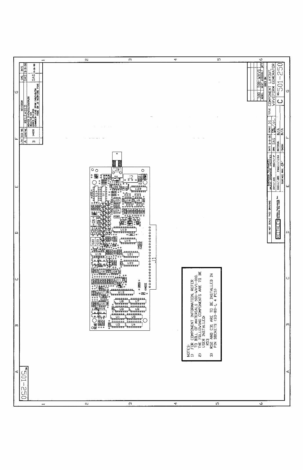
Figure 1. WAVI Module Optional Resistor R53
Mounting Bracket
Specifications
Programmable Features:
Functions: waveform, frequency, amplitude, duty cycle, DC offset, haver waveforms.
Waveforms: sine, square, triangle, pulse, or DC output.
Frequency: O.lHz to 2OOkHz in six overlapping ranges.
Frequency ranges: 2,20,200,2k, 2Ok, 200k Hz
Frequency resolution: 12 bits (1 part in 4096)
Frequency accuracy: (upper 90% of range) f5% of setting, except +lO% on 2kHz and 2OkHz ranges.
Amplitude ranges: IV, IOV peak, switch selectable
Amplitude resolution: 12 bits (1 part in 4096)
WAVl-2
,
Amplitude accuracy: rt5% of setting to 5OkHz’
Offset ranges: +lV, +lOV (tied to amplitude ranges)
Offset resolution: 13 bits (12 data + 1 polarity)
Offset accuracy: .(5% of setting + 1OmV)’
Maximum output: rtlOV (2OV p-p) into 5OOQ 2OmA
Waveform symmetry: 5% to 95% (duty cycle) to 1OOkHz
Sine wave distortion: 1st harmonic down 35dB
Square wave rise time: lp
Triangle linearity: ~3% error
* Total error is the sum of amplitude and offset errors. For DC-only operation, set waveform amplitude to 0 and use offset error, only.

WAVl Waveform Generator Module
Sync output: high and low true, TTL level, ps pulse width. Sync pulse occurs at minima of sine and triangle waves, or at falling edge of square wave.
General:
Operating temperature: 0°C to 7O”C, 80% RH non-con- densing down to 35°C
Storage temperature: -25°C to 80°C
Power-up condition: OV output
--- -. _--_ Rower consumption: 65mA for 5V dig&d, 85rd for +15V analog
Signal connections: BNC for main output, quick-discon- nect screw terminals for main and sync output.
Accessories: 2 ft. BNC to BNC cable, Model 7051-2,3 ft. BNC to BNC cable, Model 7054-3
Installation
The WAVl can be placed in any slot in the system. If the trigger output is to be used to control the operation of an ATiBaI,,TDPI --2--l- L~^T*fA~fl----rL--l---=-=~ ----. I I+IVLIVL ~1 I AU I ~~uuure, ule vv n v 1 muss ue placea aajacenr to that module, in the next higher-numbered slot.
CAUTION Turn off power to the data acquisition system before you insert or remove any module. To minimize the possibility of EM1 radiation, always operate the data acquisition system with the cover in place and properly secured.
CAUTION Make sure you have discharged any static charges on your body before handling the module. You can do this most easily by simply touching the chassis of a computer or data acquisition mainframe which is plugged into a grounded, 3-wire outlet. Avoid touching components or the card edge connector of the module.
For a compatible multi-slot data acquisition system (Model 5OOA, 5OOl?), remove the top cover of the system by loosen-
ing the cover retaining screws located in the upper corners of the rear panel. Slide the cover back about one inch and then lift it off. Insert the module in the desired slot with the component side facing the system power supply. Replace the system cover.
For a Model 570, install the module in the option slot with the component side of the board facing upward. Close and secure the cover.
For a Model 575, first attach the supplied right-angle bracket to the module (see Figure 2). Plug the module into the option dot with the components facing upward, and secure the bracket to the rear panel of the system. Close and secure the cover.
Connections
The output waveform is available on a standard BNC connector or from outputs on a screw terminal block.
A quick-disconnect terminal block can be removed from the module to facilitate making connections. PuB the block straight off the board with a firm, even pressure. Do not pry the terminals with a screwdriver or sharp object, or you -_- --- J-.-- - - .I- -? ~~ . . 1~ 1 may aamage me cucun ooara.
Each individual terminal consists of a small metal block with a wire receptacle containing a metal compression tab. To make connections to a terminal block, first strip 3/16 of insulation from the end of the wire which you want to attach. Loosen the desired terminal screw on the block and insert the bare end of the wire into the corresponding receptacle. Tighten the screw securely to compress the tab against the wire.
After you have attached all the desired signal wires to a terminal block, replace the block by lining it up with the mating pins on the module and pressing it back into place.
Table 1. WAVl User-Configured Components
Cl
WAVI-3
WAVl Waveform Generator Module
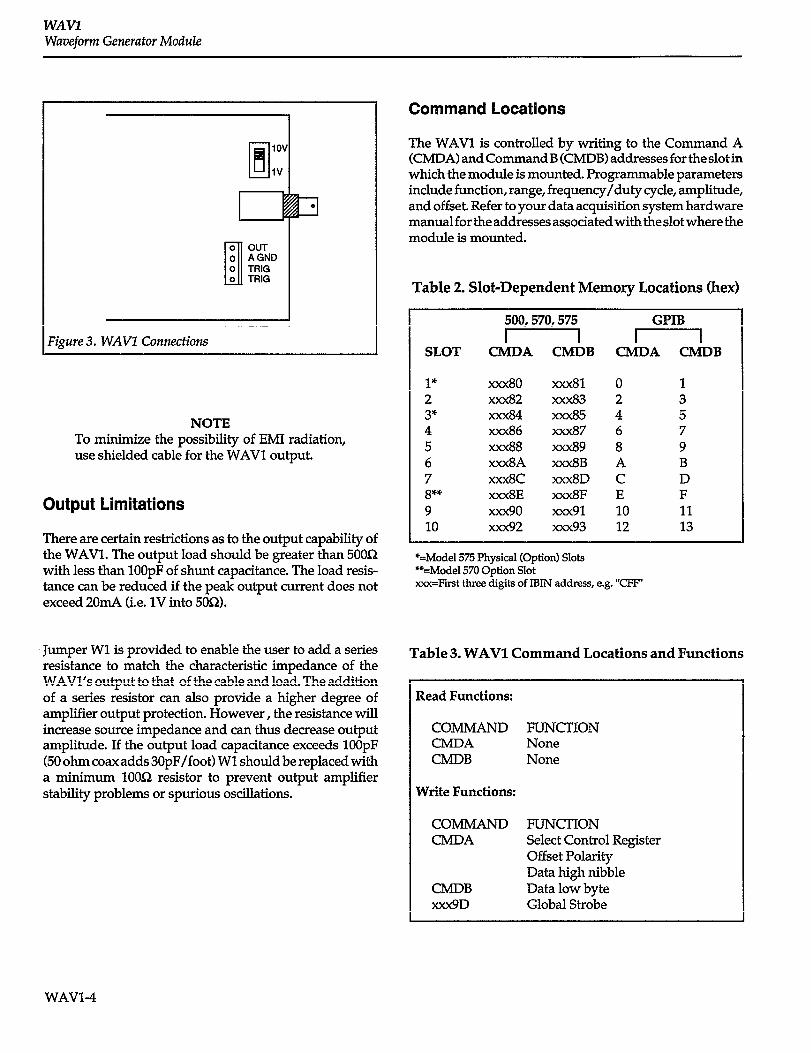
1 rigure 3. WAVI Connecfions
NOTE To minimize the possibility of EMI radiation, use shielded cable for the WAVl output.
Output Limitations
There are certain restrictions as to the output capability of the WAVL The output load should be greater than 5OOQ with less than 100pF of shunt capacitance. The load resis- tance can be reduced if the peak output current does not exceed 2OmA (i.e. 1V into 5052).
Jumper WI is provided to enable the user to add a series resistance to match the characteristic impedance of the WAVl’s output to that of the cable and load. The addition of a series resistor can also provide a higher degree of amplifier output protection. However, the resistance will increase source impedance and can thus decrease output amplitude. If the output load capacitance exceeds 1OOpF (50 ohm coax adds BOpF/foot) Wl should be replaced with a minimum 1OOQ resistor to prevent output amplifier stability problems or spurious oscillations.
Command Locations
The WAVl is controlled by writing to the Command A (CMDA) and Command B (CMDB) addresses for the slot in which the module is mounted. Programmable parameters include function, range, frequency/duty cycle, amplitude, and offset. Refer to your data acquisition system hardware manual for the addresses associated with the slot where the module is mounted.
Table 2. Slot-Dependent Memory Locations (hex)
SLOT
1* xxx80 xxx81 2 xxx82 xxx83 3” xxx84 xxx85 4 xxx86 xxx87 5 xxx88 xxx89 6 xxx8A xxx8B 7 xxx8C xxx8D 8”* xxx8E xxx8F 9 xxx90 xxx91 10 xxx92 xxx93
500,570,575 I I
CMDA CMDB
GPIB I I
CMDA CMDB
0 1 2 3 4 5 6 7 8 9 A B C D E F 10 11 12 13
*=Model575 Physical (Option) Slots **=Model570 Option Slot xxx=First three digits of IBIN address, e.g. “CFF’
Table 3. WAVl Command Locations and Functions
Read Functions:
COMMAND CMDA CMDB
Write Functions:
COMMAND CMDA
CMDB xxx9D
FUNCTION None None
FUNCTION Select Control Register Offset Polarity Data high nibble Data low byte Global Strobe
WAVl-4

WAVI Waveform Generator Module
CMDNCMDB (WRITE)
8038 -_I___ Waveform
I----
2/
Generator AU-L
Waveform Select
L
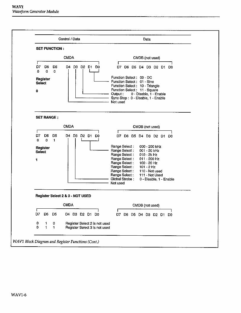
‘igure 4. WAVI Block Diagram and Register Funcfions
To ND ‘Module
e Data Bus
- Control Line
Analog Pathway
WAVl-5
WAVl Waveform Generator Module
Control I Data Data
SET FUNCTION :
I
CMDA
I
CMDB (not used)
I I D7 D6 D5 C 0 0 0
Register Select
0
14
I
D3 D2 Dl DO D7 D6 D5 D4 D3 D2 Dl Do
I I LI-’
L Function Select : 00 - DC Function Select : 01 - Sine Function Select : 10 - Triangle Function Select : 11 - Square output : 0 - Disable, 1 - Enable Sync Stop : 0 - Disable, 1 - Enable Not used
SET RANGE :
I
CMDA
I
CMDB (not used)
I I D7 D6 D5 I 0 0 1
Register Select
1
I D2 Di DO D7 D6 I x
-c F2:: E:i Range Select Range Select Range Select
i D4 D3 D2 Dl DO
000 - 200 kHz 001 - 20 kHz 010 - 2k Hz 011 -200 Hz 100 -20 Hz
Range Select : 101 -2Hz Range Select : 110-Notused Range Select : 111 -NotUsed Global Strobe : 0 - Disable, 1 - Enable Not used
Register Select 2 & 3 - NOT USED
CMDA CMDB (not used)
I I I I D7 D6 D5 D4 D3 D2 Di DO D7 D6 D5 D4 D3 D2 Dl DO
0 1 0 Register Select 2 is not used 0 1 1 Register Select 3 is not used
WAVZ Block Diagram and Register Funcfions (Cont.)
WAV1-6
WAVI Waveform Generafor Module
Control / Data Data
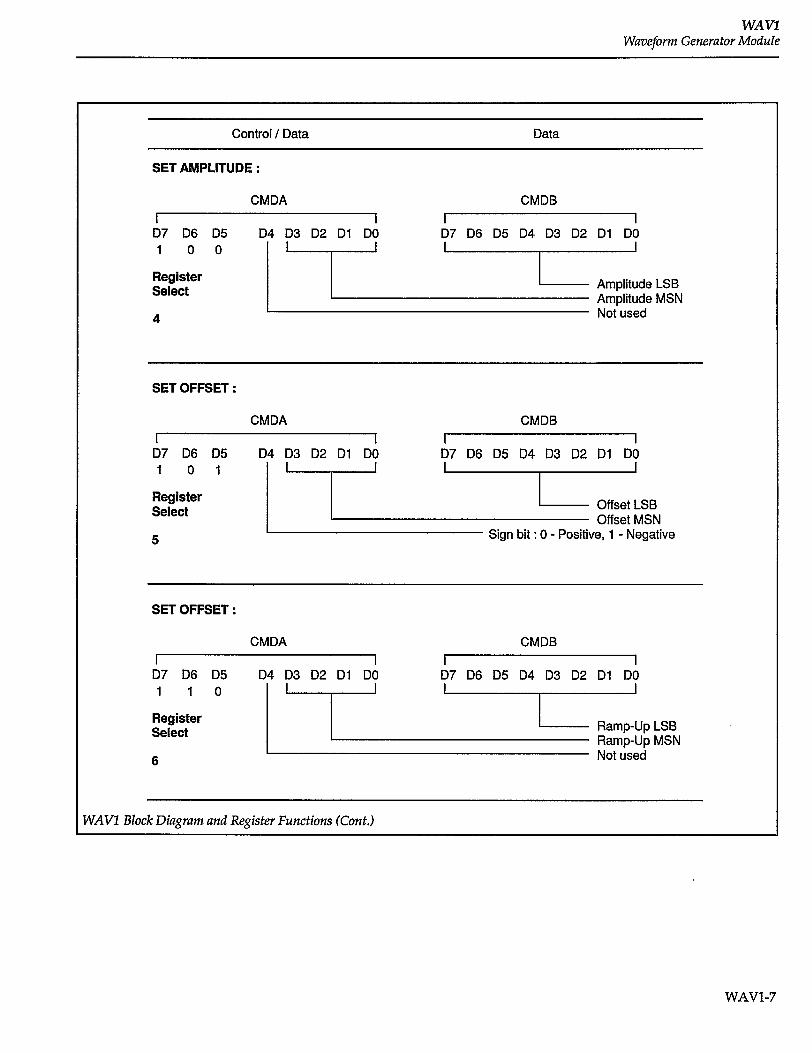
SET AMPLITUDE :
CMDA CMDB
I I I I 07 D6 D5 D4 D3 D2 Dl DO D7 D6 D5 D4 D3 D2 Di DO
’ O O
Register Select
4
SET OFFSET :
CMDA CMDB
I I I I D7 D6 D5 D4 D3 D2 Dl DO D7 D6 D5 D4 D3 D2 Di DO
SET OFFSET :
CMDA CMDB
I I I I D7 D6 D5 D4 D3 D2 Di DO D7 D6 D5 D4 D3 02 Dl DO
’ -’ O
Regmter Select
6
WAVZ Block Diagram and Register Functions (Cont.)
WAVI-7
WAVl Waveform Generator Module
1 NAVl Block Diaqam and Register Functions (Cont.)
Control / Data Data
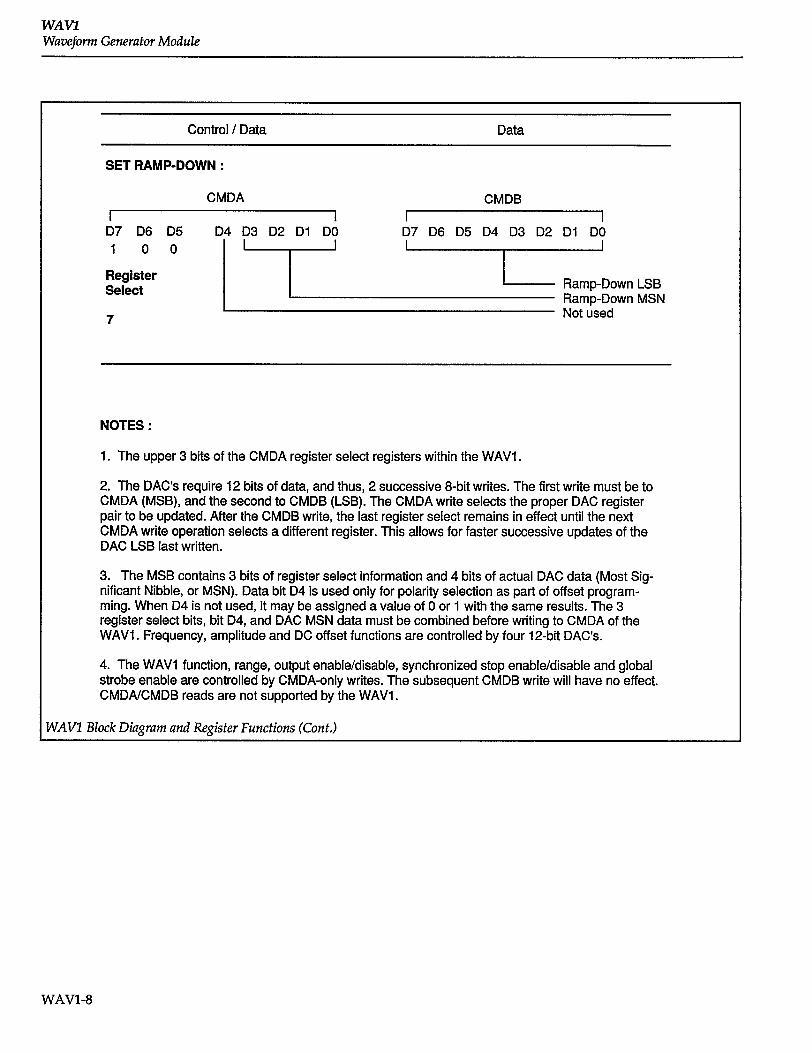
SET RAMP-DOWN :
CMDA CMDB I I I I D7 D6 D5 D4 D3 D2 Dl DO D7 D6 D5 D4 D3 D2 Dl DO 1 0 0 IV I
Register Select
7
Ramp-Down LSB Ramp-Down MSN Not used
NOTES :
1. The upper 3 bits of the CMDA register select registers within the WAVI .
2. The DAC’s require 12 bits of data, and thus, 2 successive 8-bit writes. The first write must be to CMDA (MSB), and the second to CMDB (LSB). The CMDA write selects the proper DAC register pair to be updated. After the CMDB write, the last register select remains in effect until the next CMDA write operation selects a different register. This allows for faster successive updates of the DAC LSB last written.
3. The MSB contains 3 bits of register select information and 4 bits of actual DAC data (Most Sig- nificant Nibble, or MSN). Data bit D4 is used only for polarity selection as part of offset program- ming. When D4 is not used, it may be assigned a value of 0 or 1 with the same results. The 3 register select bits, bit D4, and DAC MSN data must be combined before writing to CMDA of the WAVl . Frequency, amplitude and DC offset functions are controlled by four 1 e-bit DAC’s.
4. The WAVI function, range, output enable/disable, synchronized stop enable/disable and global strobe enable are controlled by CMDA-only writes. The subsequent CMDB write will have no effect. CMDAICMDB reads are not supported by the WAVl .
WAVI-8
WAVI Wavefom Generafor Module
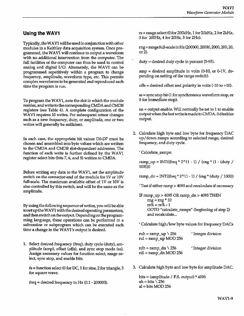
Using the WAVI
Typically, the WAVl will be used in conjunction with other modules in a Keithley data acquisition system. Once pro- grammed, the WAVl will continue to output a waveform with no additional intervention from the computer. The full facilities of the computer can thus be used to control analog and digital I/O. Alternately, the WAVl can be programmed repetitively within a program to change frequency, amplitude, waveform type, etc. This permits complex waveforms to be generated and reproduced each time the program is run.
To program the WAVI, note the slot in which the module resides, and write to the corresponding CMDA and CMDB registers (see Table 4). A complete configuration of the WAVl requires 10 writes. For subsequent minor changes such as a new frequency, duty, or amplitude, one or two writes will generally be sufficient.
In each case, the appropriate bit values DO-D7 must be chosen and assembled into byte values which are written to the CMDA and CMDB slot-dependent addresses. The function of each write is further defined by the WAVl register select bits (bits 7,6, and 5) written to CMDA.
Before writing any data to the WAVl, set the amplitude switch on the connector-end of the module for 1V or 1OV full-scale. The maximum available offset of 1V or 1OV is also controlled by this switch, and will be the same as the amplitude.
By using the following sequence of writes, you will be able to set up the WAVl with the desired operating parameters, and then switch on the output. Depending on the program- ming language, these operations can be performed in a subroutine or subprogram which can be executed each time a change in the WAVl’s output is desired.
1. Select desired frequency (freq), duty cycle (duty), am- plitude (amp), offset (offs), and sync stop mode (ss). Assign necessary values for function select, range se- lect, sync stop, and enable bits.
fs = function select (0 for DC, 1 for sine, 2 for triangle, 3 for square wave.
freq = desired frequency in Hz (0.1 - 200000).
rs = range select (0 for 2OOkHz,l for 2OkHz,2 for 2kHz, 3 for 2OOHz, 4 for 2OHz,5 for 2H.z).
mg = range full-scale in Hz (200000,20000,2000,200,20, or 2).
duty = desired duty cycle in percent (5-95).
amp = desired amplitude in volts (O-10, or 0-lV, de- pending on setting of the range switch).
offs = desired offset and polarity in volts (-10 to +lO).
ss = sync stop bit (1 for synchronous waveform stop, or 0 for immediate stop).
en = output enable. Will normally be set to 1 to enable output when the last write is made to CMDA. 0 disables output.
2. Calculate high byte and low byte for frequency DAC up/down ramps according to selected range, desired frequency, and duty cycle.
’ Calculate-ramps:
ramp-up = INT((freq * 2*11- 1) / (rng * (1 - (duty / 1om
ramp-dn = lNT((freq * 2*11- 1) / (mg * (duty / 100)))
’ Test if either ramp > 4095 and recalculate if necessary
IF ramp-up > 4095 OR ramp-dn > 4095 THEN rng=rng”lO 13% = rs% - 1 GOT0 “calculate_ramps” (beginning of step 2) and recalculate...
’ Calculate high/low byte values for frequency DACs
ruh = ramp-up \ 256 ml= ramp-up MOD 256
’ Integer division
rdh = ramp-dn \ 256 rdl = ramp-dn MOD 256
‘ Integer division
3. Calculate high byte and low byte for amplitude DAC.
bits = (amplitude / F.S. output) * 4095 ah = bits \ 256 al = bits MOD 256
WAVl-9
WAVl Waveform Generator Module
(F.S. output = 1 or 10, depending on range switch position.)
4. Calculate high byte and low byte for offset DAC .
bits = tabs. value (offs / F.S. offset)) * 4095 oh=bits\256 01 = bits MOD 256 op = offset polarity (0 for pos, 1 for neg)
(F.S. offset = 1 or 10, depending on range switch posi- tion.)
5. Do the POKES
’ POKE high and low bytes to the ramp-down DACs. ’ Register select = 7
POKE cmda, (7 * 32) + rdh POKE cmdb, rdl
’ POKE high and low bytes to the ramp-up DACs ’ Register select = 6
POKE cmda, (6 * 32) + rub POKE cmdb, rul
’ POKE high and low bytes to the offset DACs ’ Register select = 5
POKE cmda, (5 * 32) + (op * 16) + oh POKE cmdb, 01
’ POKE high and low bytes to the amplitude DACs ’ Register select = 4
POKE cmda, (4 * 32) + ah POKE cmdb, al
’ POKE range and global strobe values ’ Register select = 1
l?OKEcmda,(1*32)+gs*8+rs
’ POKE sync stop, output enable, and function ’ Register select = 0
POKE cmda, (0 * 32) + (ss * 8) + (en * 4) + fs
The following discussions cover a few of the operating parameters where necessary details are not immediately obvious.
WAVl-10
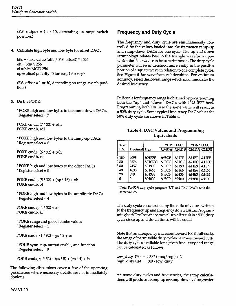
Frequency and Duty Cycle
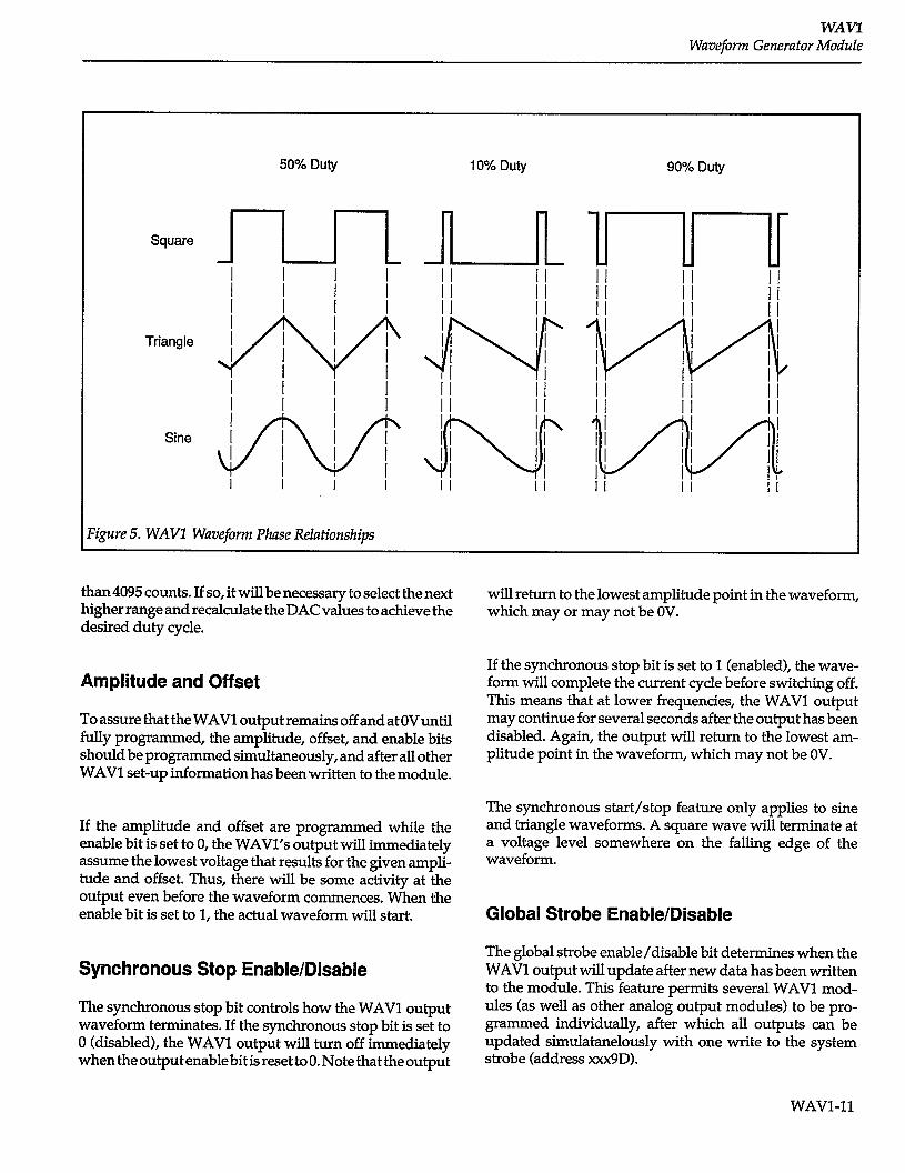
The frequency and duty cycle are simultaneously con- trolled by the values loaded into the frequency ramp-up and ramp-down DACs for one cycle. The up and down terminology relates best to the triangle waveform upon which the sine wave can be superimposed. The duty cycle parameter can be understood more easily as the positive portion of a square wave in relation to one complete cycle. See Figure 5 for waveform relationships. For optimum accuracy, select the lowest range which accommodates the desired frequency.
Full-scale for frequency range is obtained by programming both the “up” and “down” DAC’s with 4095 (FFF hex). Programming both DACs to the same value will result in a 50% duty cycle. Some typical frequency DAC values for 50% duty cycle are shown in Table 4.
Table 4. DAC Values and Programming Equivalents
% of F.S. Decimal Hex
100 4095 &HFFF 80 3276 &HCCC 60 2457 c&H999 40 1638 &H666 20 819 &H333
0 0 &HO00
&HCF &HCC &HC9 &HC6 &HC3
&HCO
&HFF M-ICC &H99 @I66 c&H33
&HO0
&HEF &HEC &HE9 &HE6 &HE3
&HE0
DAC CMDB
&HFF &HCC &H99 &H66 &H33
&HO0
Note: For 50% duty cycle, program “w” and “DN” DAC’r same values.
1
The duty cycle is controlled by the ratio of values written to the frequency up and frequency down DACs. kogram- ming both DACs to the same value will result in a 50% duty cycle since up and down times will be equal.
Note that as a frequency increases toward 100% full-scale, the range of permissible duty cycles narrows toward 50%. The duty cycles available for a given frequency and range can be calculated as follows:
low-duty (%) = 100 * ( freq/rng > / 2 high-duty (%) = 100 - low-duty
At some duty cycles and frequencies, the ramp calcula- tions will produce a ramp-up or ramp-down value greater
WAvl Wavefom Generator Module
50% Duty 10% Duty 90% Duty
Square
Triangle
Sine
3gure 5. WAVl Wavefom? Phase Relationships
than 4095 counts. If so, it will be necessary to select the next higher range and recalculate the DAC values to achieve the desired duty cycle.
Amplitude and Offset
To assure that the WAVl output remains off and at OVuntil fully programmed, the amplitude, offset, and enable bits should be programmed simultaneously, and after all other WAVl set-up information has been written to the module.
If the amplitude and offset are programmed while the enable bit is set to 0, the WAVl’s output will immediately assume the lowest voltage that results for the given ampli- tude and offset. Thus, there will be some activity at the output even before the waveform commences. When the enable bit is set to 1, the actual waveform will start.
Synchronous Stop Enable/Disable
The synchronous stop bit controls how the WAVl output waveform terminates. If the synchronous stop bit is set to 0 (disabled), the WAVl output will turn off immediately when the output enable bit is reset to 0. Note that the output
will return to the lowest amplitude point in the waveform, which may or may not be OV.
If the synchronous stop bit is set to 1 (enabled), the wave- form will complete the current cycle before switching off. This means that at lower frequencies, the WAVl output may continue for several seconds after the output has been disabled. Again, the output will return to the lowest am- plitude point in the waveform, which may not be OV.
The synchronous start/stop feature only applies to sine and triangle waveforms. A square wave will terminate at a voltage level somewhere on the falling edge of the waveform.
Global Strobe Enable/Disable
The global strobe enable/disable bit determines when the WAVl output will update after new data has been written to the module. This feature permits several WAVl mod- ules (as well as other analog output modules) to be pro- grammed individually, after which all outputs can be updated simulatanelously with one write to the system strobe (address xxx9D).
WAVl-11
WAVI Waveform Generator Module
The WAVl functions associated with the global strobe are those functions controlled by D/A converters: amplitude, frequency, and offset. If the global strobe feature is en- abled, the WAVl DAC-related functions will not update until a global strobe pulse has been issued by the data acquisition system. If the WAVl global strobe feature is disabled, any new information will take effect immedi- ately when is written to the WAVl module.
Haversine Pulse
A haversine is a single sine output pulse, e.g. a pulse with sinusoidal shape which rises from the minimum ampli- tude point, reaches the maximum amplitude, and decays back to the minimum. WAVl haver pulses should be programmed for sine and triangle waves. Programming a haver square wave can result in the output pulse terminat- ing at any point along the trailing edge of the pulse, rather than at minimum amplitude.
Haver pulses can be performed by first doing the usual set- up writes to WAVl registers 7,6,5,4, and 1 as shown above. Next, a write must be made to register 0 to simultaneously set the desired amplitude and turn on the sync stop and output enable bits. This write should be followed immedi- ately by another write to register 0 which turns off the output enable bit. Since the sync stop feature is enabled, one complete pulse should result at the output.
The speeds which can be achieved for haver pulses depend on the speed of the computer and the speed at which the output enable and disable writes can be executed. In this respect, performance improves dramatically under a compiler language. A 1OMHz 286 computer executing a compiled (.EXE) file can fire a single haversine pulse at 2ookJsz.
An oscilloscope can be used to examine the ouput of the WAVl at higher frequencies. If the speed of the language or computer is insufficient for haver pulses at a given frequency, multiple pulses will be generated and observed on the scope.
Using the WAVI as a DC Bias Source.
The WAVl can be used as a DC bias source with up to 2OmA of output current capability. The DC output func- tion must be selected, and the desired DC level must be programmed as offset (refer back to programming the
WAVl-12
offset DAC high and low bytes and polarity). The DC level will appear at the WAVl output when the output enable bit is turned on. The frequency and amplitude DACs have no effect in this mode of operation, and should beset to 0 when the WAVl is used for DC output.
Notes:
1.
2.
The WAVl specifications are valid only with an AMM installed in slot 1. If the WAVl is intended for use in a system that does not contain an AMM, an optional resistor 5K ohm 0.1% 0X53, included) must be installed. See the component layout for the location of R53. The WAVl output signal will contain some spurious noise. Some of the noise is generated by the mainframe into which the WAVl is installed, some by the WAVl itself. a.
b.
C.
The WAVl generated noise will be at a maximum with the output amplitude set to a minimum (~1% of ES.), and the square wave function or synchro- nous stop functions selected. This noise is caused by capacitive coupling through the amplitude attenu- ator DAC. Since it is capacitively coupled, the noise will be more pronounced at higher programmed frequencies. Selecting sine, triangle or DC wave- forms will reduce the noise. System-induced noise may be reduced by using a shielded BNC cable from the WAVl. Any unsh- ielded wires connected to the WAVl can also couple additional noise onto the output. A low-pass filter may be added to the input of the driven device to further reduce the amplitude of any noise present.
Calibration
This section contains general field calibration information for the WAVl. The procedures given are not necessarily as accurate as factory calibration. Also, the procedures given assume a certain amount of expertise on the part of the user. If you are not familiar with calibrating equipment, do not attempt calibration. The procedures in this section assume that you are familiar with general module opera- tion. Refer to the appropriate manual for details on cali- brating each module.
The WAVl has four calibration adjustments; ramp-up zero, ramp-up gain, ramp-down zero and ramp-down gain. The adjustments are somewhat interactive and there- fore must be performed in the proper order for calibration to be achieved.
WAvl Waveform Generator Module
The ramp zero and gain interact with one another in addition to the ramp-up zero and gain affecting the ramp- down zero and/or gain. The ramp-down adjustments do not, however, affect the ramp up adjustments.
Required equipment:
4-l/2 digit DVM, accuracy better than 0.1%. Frequency Counter with pulse period capability.
Environment: 23°C zEPC, less than 35% R.H., non-con- densing
NOTE The WAVl specifications are valid only with a calibrated AMhI installed in slot 1 providing a VRRF of +lO volts to the WAVl.
Procedure (refer to the component layout Figure 1 for location of test points and calibration controls).
1. Adjust ramp zero voltage for OV f5mV on TP4 and Tl?5 using Rl?l and RP2.
2. Program the WAVl to output a500Hz square wave, full scale amplitude, zero DC bias.
3. Connect the frequency counter to the BNC output and set to measure pulse low width. The square wave is low during the ramp-up portion of the sine and triangle waveforms.
4. Adjust ramp-up zero (RPl) for l.OOms kO2ms reading on the frequency counter.
5. Program the WAVl to output a 2000Hz square wave. 6. Adjust ramp-up gain (Rl?3) for 250~ E$s. 7. Repeat steps 2 through 6 until the readings remain
within specified limits. 8. Program the WAVl to output a5OOHz square wave, fuh
scale amplitude, zero DC bias. 9. Set counter to measure pulse high width. 10. Adjust ramp-down zero (RP2) for l.OOms k02ms read-
ing on the frequency counter. 11. Program the WAVl to output a 2OOOHz square wave. 12. Adjust ramp-down gain (RP4) for 250~ k5~. 13. Repeat steps 8 through 12 until the reading remains
within specified limits.
14. Verify all four calibration points remain within specifi- cations. Repeat entire procedure if necessary to obtain convergence.
Performance Verification
Required equipment:
4-l/2 digit DIM, accuracy better than 0.1% Oscilloscope with 2OMHz bandwidth. MHz frequency counter. AMMIA or AMM2 in slot 1 supplying reference
Procedure (Global strobe disabled for all tests, 1OV range)
1. Program the WAVl for DC function, output disabled, 2OOKHz range, OHz frequency, OV amplitude and OV offset. Set the range DC function switch to 10Vposition.
2. Connect DVM and Scope (counter optionally) to main output.
3. Observe DVM, reading should be less than flOmV. 4. Observe scope, output should be DC with no signifi-
cant oscillations present. 5. Program +lV offset. 6. Observe DVM, reading should be 1V +_15mV. 7. l?rogram -lV offset. 8. Observe DVM, reading should be -IV fl5mV. 9. Repeat steps 5 through 8 for programmed and ob-
served values of k2, k5, +lOV. Substitute appropriate errors based on amplitude.
10. Program the WAVl for Triangle function, output en- abled, 2OOKHz range, 2OORHz frequency, 1V ampli- tude and OV offset.
11. Observe scope, output should be a IV peak, 200 KHz triangle wave. Use the counter to determine whether the output is within specified limits.
12. Repeat steps 10 and 11 for all full scale frequencies on the five remaining ranges.
13. Repeat steps 10 through 12 for 2V, 5V and 1OV ampli- tudes.
14. Repeat steps 10 through 12 for sine and square wave functions. Random sampling of 10% and 50% of fuh scale frequencies and amplitudes can be performed to the testers satisfaction.
15. Program the output for DC function, IV offset. 16. Set range switch to 1V range position. 17. Observe DVM reading .lV rtllmV.
WAVl-I.3
WAVl Waveform Generator Module
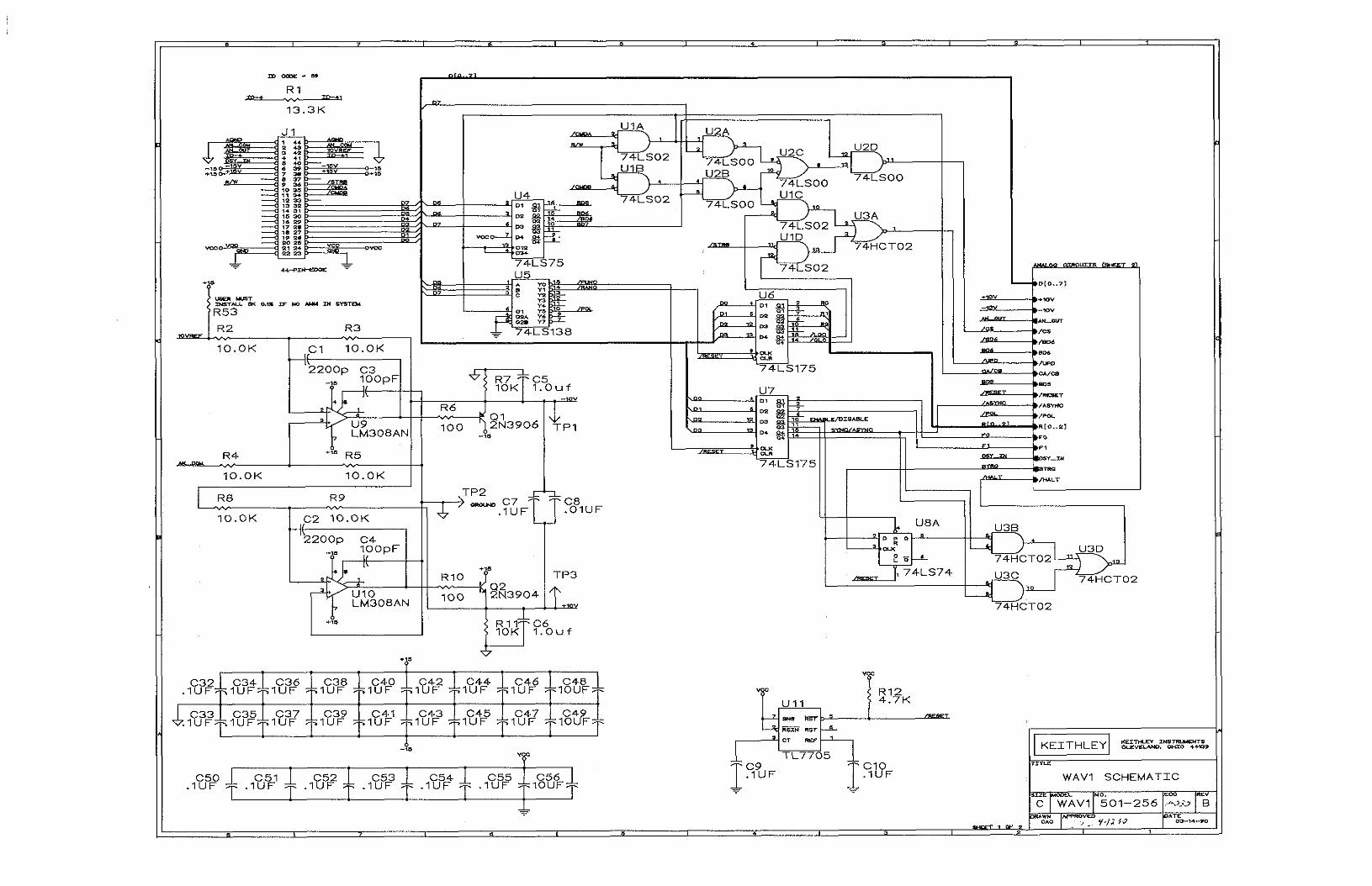
Theory of Operation
WAVl operation involves analog as well as digital cir- cuitry.
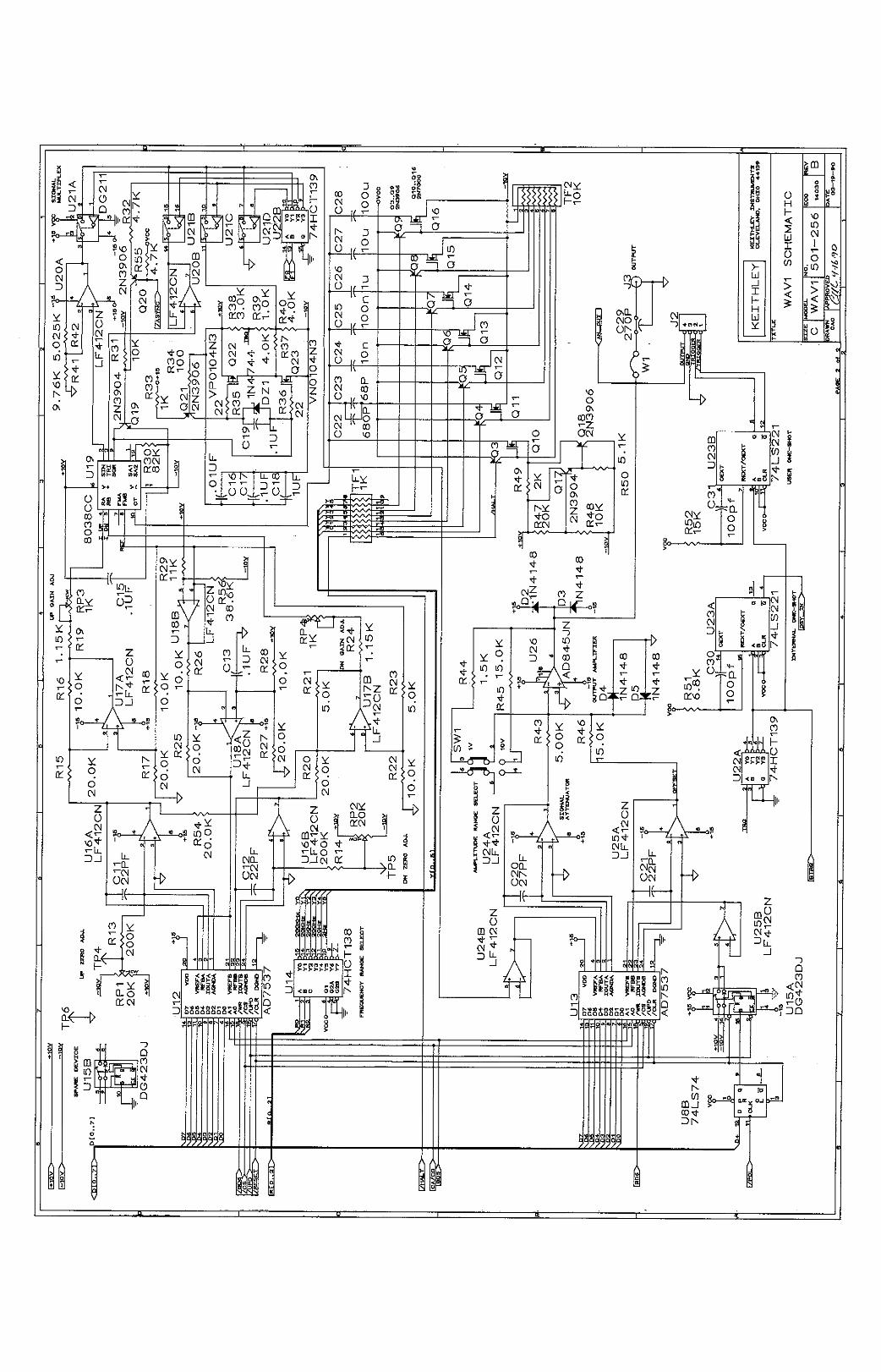
Analog
TheWAVlisbasedonafunctiongeneratorIC,theICL8038. The IC provides the following facilities necessary for the operation of the WAVl:
2 switchable current sources 2 comparators for control of current sources Triangle wave to sine wave conversion Square wave output
The current sources are varied to control the magnitudes of their charge and discharge currents. The ramp-up and ramp-down times, and thus the frequency and duty cycle, are varied in this way. The ratio of the values of the two current sources determine the output duty cycle. The cur- rent sources are controlled by dual D/A converter U12. These are two 12-bit DAC’s with their reference inputs supplied by U19, the 8038. This reference is buffered by U18B and level shifted referenced to analog ground by differential amplifier U18A. The reference voltage is essen- tially divided by the value programmed into each of the two DAC’s to produce an output current which is subse- quently converted back into a voltage by amplifiers Ul6A and U16B. The scaled DAC output voltages are fed to differential amplifiers U17A and U17B which level shift, relative to the 8038’s reference output, and feed the current source control inputs of the 8038.
The 8038 switches the appropriate current source onto the timing capacitor connected to pin 10. The value of the capacitor determines the range of available frequencies. The available values of range capacitors are -1OOOpF to 1OOpF. These values correspond to frequency ranges from 2OOKHz to 2Hz respectively. The group of analog switches comprised of transistors Q3 through Q16 switch the se- lected capacitor onto 8038 pin 10.
The three outputs of the ICL8038 are normalized to 3.333 volts peak, buffered and fed to a four line multiplex switch comprised of U21 and U22B. The triangle output, essen- tially the capacitor voltage, is impedance buffered by am- plifier U20B. The sine wave output, having a slightly
reduced amplitude compared to the triangle wave, is buff- ered and amplified slightly by U20A. The square wave output is buffered by a complimentary MOSFET amplifier composed of transistors 421 through 423. A resistor di- vider composed of R37 through R40 scales the square wave to 3.333 volts peak.
The mux output is buffered byU24B and fed to DAC U13A. The output of U13A and I-V conversion amplifier U24A is proportional to the digital code programmed into U13A given a 3.333V peak input. The main signal is fed to the WAVl’s output amplifier U26, which has a gain of 3 or .3 depending on range switch setting, resulting in a maxi- mum output of 1OV or IV peak respectively. DAC Ul3B, reference selector switch U15A, buffer U25B, and I-V am- plifier U25A provide a 10 volt bipolar signal which is summed into the main signal path with an effective gain of 1 or 0.1, depending on range switch setting, thus biasing theoutputsignalonaDCvoltageoflOVorlVrespectively.
US, UlO and associated circuitry provide plus and minus 10 volt reference supplies. The output transistors Ql and Q2 provide additional current driving capability.
Ull and associated circuitry provide a low-true reset pulse on power-up and down transitions.
U23A one-shot provides a 500ns low-true pulse on every negative transition of the main square wave output. This signal is fed exclusively to the system baseboard daisy chain bus in the direction of slot 1 @MM). U23B one-shot provides lo& complimentary pulses to the user connector J2. The PC board is designed to accept a potentiometer and resistor to allow the user to vary the output pulse width.
Digital
Logic gates Ul, U2 and U3 decode the baseboard control signals for interfacing with the DAC’s, function and range select registers. U4 is a transparent latch that holds the three most significant data bits last selected by a CMDA write. U5 decodes chip selects from the 3 MSB’s and feeds them to U6, range register, U7 function register and U8B offset polarity register. Register U7 contains output en- able/disable and synchronous stop enable/disable bits in addition to function select bits. The remainder of the de- coding is done by the DAC internal gating circuitry.
WAVI-14

WAVl Waveform Generator Module
Troubleshooting
Any observed or suspected problem with a system or module may be the result of malfunctions in any part of the system. A hierarchy of possible problem areas is listed below. The list should help you apply an organized ap- proach to troubleshooting, starting with software and working toward a specific module. It assumes that your system and software have both worked properly in the past. If you have spares, you can most quickly verify a system component through simple substitution. Check your data acquisition system manual or computer docu- mentation -they may contain additional instructions on troubleshooting.
1. Faulty software or applications programs - If you have completed a new program which does not work as anticipated, review the program design and be certain that it actually functions as you assume. If a program which had been running properly begins to behave erratically, either the supporting software package or the application program may have been corrupted. This may occur through disk media failures, power supply problems, hardware failures, or operator error.
Verify your software package against a back-up copy or the original diskettes. If the software is questionable, you should reinstall the software from the original diskettes or known-good copies. Likewise, your appli- cations program should be restored from backups if a problem develops. Note that it is crucial to back up important software and programs. Ideally, you should make at least two copies, and store one in a location away from your work site. Application programs should be backed up regularly as they are being developed. Printouts of program listings may also be desirable.
2. Faulty computer system - A malfunctioning computer or peripheral can affect the data acquisition software and hardware, ranging from minor problems to total failure. These problems may be continuous or intermit- tent. If you suspect your computer, remove the data acquisition interface and run any diagnostics which came with the system to verify its performance. Also try running other software with which you are familiar. Pay close attention for any erratic behavior of the software which may indicate hardware problems.
3. Defective interface-A malfunctioning data acquisition interface can prevent the computer from booting up and operating properly, or it can affect only the data acquisition system. Some graphics, mouse, and net- working adapters conflict with data acquisition inter- faces as a result of both using the same addresses or interrupts. The system operates properly with one of the cards in place, but diagnostic error messages or
other problems result with both cards plugged in. You can usually determine incompatibility by trying each suspected card individually, and then together. Such incompatibility can often be overcome through switch settings, configuration changes, or minor modifica- tions to the hardware.
4. Defective data acquisition interface cable - The cable carries essential power, control, or data signals. Open conductors in a cable will disrupt the process. Cable shorts, especially in lines carrying system power sup- ply voltages, may cause a total shutdown of the com- puter or data acquisition mainframe. If these problems exist, try disconnecting the interface cable from the computer and data acquisition system.
There is a maximum permissible length specified for interface cables. Exceeding the length will also intro- duce problems. You may note erratic operation of the computer, corrupt data, or a failme of the indicator lamps on the data acquisition system to light.
5. Defective data acquisition mainframe - A mainframe defect can affect any and all data acquisition functions. Main areas include the mother board logic and connec- tors, the expansion slots, and the power supply. In the case of a completely dead acquisition system, always check any fuses and cabling which carry power.
An individual slot may also be bad. A known good module can be tried in various slots to determine the condition of individual mainframe slots.
6. Defective module(s) in general -A failure in a module’s address, data, or control circuitry can affect other mod- ules if the malfuctions ultimately reach the data acqui- sition mother board or power supply. You may be able to locate a faulty module by removing modules indi- vidually until the problem clears.
The master A/D module in slot 1 is a special case because it processes data from alI analog input chan- nels. Any analog input involves its global multiplexer, programmable gain amplifier, and A/D converter. If only the analog input functions are faulty, you should also consider the master A/D module. Use a known- good A/D module, or first verify your A/D module for proper operation before troubleshooting another ana- log module.
Analog output normally relies only on circuitry within an analog output module unless documentation for the module states otherwise. The AOM5 modules uses the IOV precision reference on the AMM module. If you note inaccurate output levels from the AOM5, the AMM module may need to be calibrated.
WAVl-15
WAVl Wavefom Generator Module
7.
Digital input and output are also performed wholly on a single module, with the exception of the PIMl and PIM2 power control modules. The PIM modules use an external board and solid state relays. These should also be considered in situations where PIM modules are suspected of being faulty.
In troubleshooting modules, use a software package with which you are familiar to write a few simple test programs for the suspected module. Elaborate pro- grams should generally not be used. They may contain their own errors which mask problems with the hard- ware.
If a suspected module does not respond as expected, you may assume that the module requires calibration or is defective. If a module has no calibratable compo- nents, a problem at this point will normally indicate a failure within the module. Defective WAV’l module - A WAVl can be checked by running a few simple programs which test individual features of the module. The CMDA and CMDB regis- ters can also be exercised to determine correct opera- tion of the module. See information elsewhere in this manual.
A skilled technician who has access to electronic test equipment may be able to troubleshoot individual circuits on a module to isolate the faulty parts. A full parts list and diagram set are included with each mod- ule to aid the technician.
If a defective component is found, replacement parts may be obtained from Keithley. If factory service is desired, the module may be returned for repair. All Keithley-manufactured systems and modules are war- ranted against defects in material and workmanship for a period of one year. For information on replace- ment parts or factory service, see the Parts List section of the appropriate manual.
NOTE The basic accuracy of the WAVl module is 5%. If a WAV which had been working properly suddenly becomes inaccurate by more than a few percent beyond nominal, the problem is more likely a malfunction and not a calibration problem. If you cannot calibrate the hardware after two attempts, you should return it to Kei- thley for repair or calibration at the factory.
List of Replaceable Parts
This section contains replacement parts information, com- ponent location drawings and schematic diagrams. Parts are listed alphanumerically in order of their circuit desig- nations.
Ordering Information
To place an order, or obtain information concerning re- placement parts, first contact the Keithley customer service department at (216) 248-0400. When ordering parts, in- clude the following information:
1. Model Number 2. Serial Number 3. Part Description 4. Circuit Designation (if applicable) 5. Keithley Part Number
If an additional instruction manual is required, order the manual package (Keithley Part Number 501-921-00). The manual package contains an instruction manual and any applicable addenda.
WAVl-16
WAVY Wavefom Generator Module
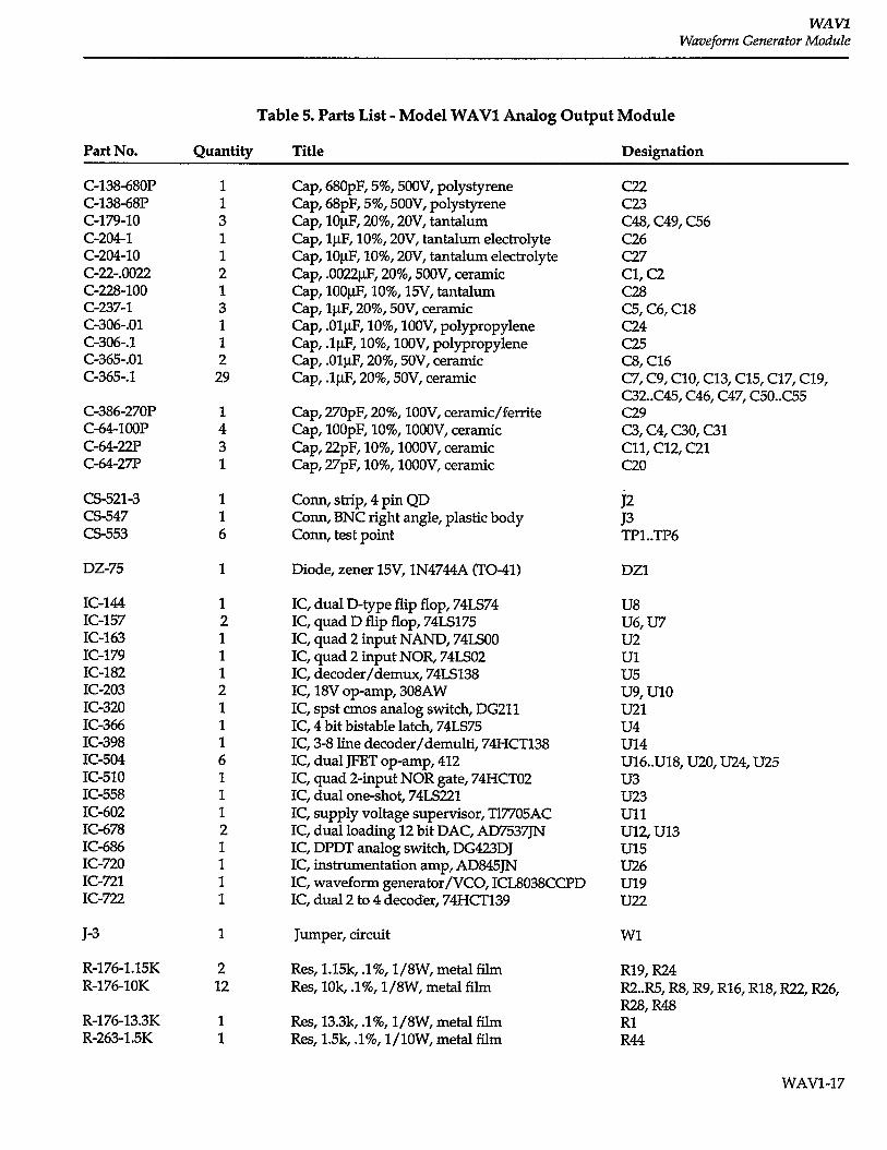
Table 5. Parts List - Model WAVl Analog Output Module
Part No. Quantity Title Designation
C-138-68OP 1 Cap, 68OpF, 5%, 5OOV, polystyrene C-138-68P 1 Cap, 68pF, 5%, 5OOV, polystyrene c-179-10 3 Cap, lOpF, 20%, 2OV, tantahxn c-204-1 1 Cap, 1pF, lo%, 2OV, tantahnn electrolyte c-204-10 1 Cap, lOpF, lo%, 2OV, tantalum electrolyte c-224022 2 Cap, .0022pF, 20%, 5OOV, ceramic C-228-100 1 Cap, lOOl.tF, lo%, 15V, tantalum c-237-1 3 Cap, lj.@, 20%, SOV, ceramic C-306-.01 1 Cap, .OlpF, lo%, lOOV, polypropylene C-306-l 1 Cap, .lj.tF, lo%, lOOV, polypropylene C-365-.01 2 Cap, .Oli.tF, 20%, SOV, ceramic C-365-l 29 Cap, .li.tF, 20%, 5OV, ceramic
C-386-270P 1 Cap, 27OpF, 20%, lOOV, ceramic/ferrite c-64-1OOP 4 Cap, lOOpF, lo%, lOOOV, ceramic C-64-22F 3 Cap, 22pF, lo%, lOOOV, ceramic c-64-27P 1 Cap, 27pF, lo%, lOOOV, ceramic
C23 C48, C49, C56 C26 C27 Cl, c2 C28 C5, C6, Cl8 C24 C25 CS, Cl6 c7, c9, ClO, c13, c15, c17, c19, C32..C45, C46, C47, C5O..C55 C29 c3, c4,00, c31 Cll, c12, C21 c20
CS-5213 1 Conn, strip, 4 pin QD cs-547 1 Corm, BNC right angle, plastic body El-553 6 Corm, test point
g TPl..TP6
DZ-75 1 Diode, zener 15V, lN4744A (TO-41) DZl
IC-144 1 IC, dual D-type flip flop, 74LS74 US IC-157 2 IC, quad D fiip flop, 74LS175 US, U7 IC-163 1 IC, quad 2 input NAND, 74LSO0 u2 IC-179 1 IC, quad 2 input NOR, 74LSO2 ul IC-182 1 IC, decoder/demux, 74LS138 u5 IC-203 2 IC, 18V op-amp, 308AW u9, UlO IC-320 1 IC, spst cmos analog switch, DG211 u21 IC-366 1 IC, 4 bit bistable latch, 74LS75 u4 IC-398 1 IC, 3-8 line decoder/demulti, 74HCT138 u14 IC-504 6 IC, dual JFET op-amp, 412 U16..UlS, U20, U24, U25 IC-510 1 IC, quad 2-input NOR gate, 74HCT02 u3 IC-558 1 IC, dual one-shot, 74LS221 U23 IC-602 1 IC, supply voltage supervisor, Tl7705AC Ull IC-678 2 IC, dual loading 12 bit DAC, AD7537JN u12, u13 IC-686 1 IC, DPDT analog switch, DG423DJ u15 IC-720 1 IC, instrumentation amp, AD845JN U26 IC-721 1 IC, waveform generator/VCO, ICL8038CCPD u19 IC-722 1 IC, dual 2 to 4 decoder, 74HCT139 U22
J-3
R-176-1.15K R-176-10K
R-176-13.3K R-263-1.5K
1
2 12
1 1
Jumper, circuit Wl
Res, l.l5k, .I%, l/SW, metal film Res, lOk, .l%, l/SW, metal film
Res, 13.3k, .l%, l/SW, metal film Res, 1.5k, .l%, l/lOW, metal film
R19, R24 R2..R5, RS, R9, R16, R18, R22, R26, R28, R48 Rl R44
WAVl-17

WAvl Waveform Generator Module
R-263-1lK R-263-15K R-263-1K R-263-20K R-263-38.6K R-2633K R-263-4K R-263-5.025K R-263-5K R-263-9.76K R-76-100 R-76-10K R-76-15K R-76-1K R-76-22 R-76-2K R-76-4.7K R-76-5.1K R-76-6.8K R-76-82K R-88-200K
RF-28
RP-89-1K RP-89-20K
SW-445
TF-177-1 TF-179-1
TG-192 TG-193 TG-195 TG-47 TG-84
501-921-OOA
1 2 1 7 1 1 2 1 4 1 3 3 1 1 2 1 3 1 1 1 2
4
2 2
1
1 1
1 1 7 3 11
1
Res, Ilk, .l%, l/lOW, metal film Res, 15k, .l%, l/lOW, metal film Res, lk, .l%, l/lOW, metal film Res, 2Ok, .l%, l/lOW, metal film Res, 38.6k, .I%, l/lOW, metal film Res, 3k, .l%, l/lOW, metal film Res, 4k, .l%, l/lOW, metal film Res, 5.025k, .l%, l/lOW, metal film Res, 5k, .l%, l/lOW, metal film Res, 9.76k, .l %, 1 /lOW, metal film Res, 100,5%, 1/4W, composition or film Res, lOk, 5%,1/4W, composition or film Res, 15k, 5%, 1/4W, composition or film Res, lk, 5%, 1/4W, composition or film Res, 22,5%, 1/4W, composition or film Res, 2k, 5%, 1/4W, composition or film Res, 4.7k, 5%, 1/4W, composition or film Res, 5.lk, 5%, 1/4W, composition or film Res, 6.8k, 5%, 1/4W, composition or film Res, 82k, 5%, 1/4W, composition or film Res, 2OOk, l%, 1 /SW, metal film
Diode, silicon, IN4148 (DO-35)
Pot, lk, lo%, .75W, non-wirewound Pot, 2Ok, lo%, .75W, non-wirewound
Switch (DPDT)
Res net, lk, 2%, 2.25W Res net, lOk, 2%, 1.3W
R29 R45, R46 R39 R15, R17, R20, R25, R27, R47, R54 R56 R38 R37,R40 R42 R21, R23, R43, R53 R41 R6, RlO, R34 R7, Rll, R31 R52 R33 R35, R36 R49 R12, R32, R55
R51 R30 R13, R14
D2, D3, D4, D5
Rr3, Rr4 RN, RP2
SW1
TF1 TF2
Trans, N-channel DMOSFET, VNO104NS(TO-92) 423 Trans, P-channel DMOSFET, Vl?O104N3(TO-92) 422 Trans, N than MOSPOW FET, 2N7000 (TO-92) QlO..Q16 Trans, NPN silicon, 2N3904 (TO-92) 42,417, Q19 Trans, l?NP silicon, 2N3906 (TO-921 QL 43-49, QW Q20, Q21
Manual package
WAVl-18
-
N
moar-a
RI 2w-’ -*,.. 1
13.3K r
lO.OK S’ lO.OK
R4 ..S--.-..
lO.OK lO.OK
UIA
& TPl
R8
lO.OK
R9
C2 lO.OK I\ 2200p c4
TP2 -
*e
c32 c34 C36 C38 c40 C42 c44 C46 C48 .lUFz,,1UF~~lUF 7~1°F =slUF 5: 1UF -ilUF >ilUF -:lOUF=
c37 c39 .lUF~i1%3?~<1UF ~71°F 75
c33 c41 c43 c45 c47 IUF 7<1UF zl”F -71°F --,l%4F?- J
-._
C52 1 C53 1 C54 1 C55 1 C56 1 .lUF T .lUF T .lUF q+ .lUF TIOUFT
TO2
74HCT02
WE
C WAVI b-256 ::m ;
I
I\ I III
Writing a Custom Driver for the WAVl Module
The WAVI module is a pro- grammable source of sine, square and triangle waves at frequencies of 0.1 to 2OOkHz and duty cycles of 5% to 95%. A DC offset function permits the module to be used as a DC bias source, or to offset the output wave- forms relative to 0 volts.
The WAVl can operating auto- nomously once it has been pro- grammed, leaving more processor time for performing acquisition, output, or data management tasks. Since the module is software- controlled, any special waveforms, modulations, etc. can be reproduced each time the program is executed.
Programming the WAVl is some- what more involved than other 500- series modules because the WAVl has a greater number of operating parameters. A complete WAVl set- up requires 10 writes, whereas most other I/O modules need only a few reads and/or writes. Once the basic WAVl configuration has been set, however, a single parameter such as frequency, amplitude, or duty cycle can be modified independently. In this regard, the WAVl is easier to program than most other modules.
A WAVl can be controlled completely through BASIC POKE statements or similar memory-write functions of other languages. While this may seem more difficult than using a high-level command, any high-level command still needs to address all the WAVl’s parameters. Further, controlling the WAVl at a primitive level offers the following advantages:
l The WAVl can be operated from any programming language, regardless of whether the language offers specific support for the WAVl. Soft500, Quick500, and earlier KDAC500 versions do not support the WAVl. Users of these packages might want to add the WAVl to their systems.
0 The user wiIl have maximum control over the WAVl. Any pre- written driver for the WAVl may make certain assumptions or com- promises. The WAVl’s extensive set of configuration parameters provides many possible methods of operating the module. Accessing the WAVl directly at the hardware level gives the programmer ultimate real-time control over the module.
Writing a Custom Driver for the WAVl Module
l Communication with the WAVl can be totally customized to the application. The program may include prompts, status messages, and error checking as needed.
A QuickBASIC Driver for the WAVl
The end of this note provides a listing for a WAVl driver written in QuickBASIC V4.5. This is an ex- ample of a general-purpose driver which can access all the WAVl’s capabilities. It can be used as a sub- program, or compiled and combined with QuickBASIC’s libraries. The listing can also be used as a guide to writing a driver in some other language. The source code can be reduced by about one fourth if the comments are omitted.
A few comments are in order concerning the driver. First, when used as a sub-program the driver must be declared “SUB” in the beginning of the main QuickBASIC program. This is accomplished with the following statement:
DECLARE SUB wavl (add&, sl%, command.string!J)
This form was chosen to simplify programming the module. The com- mand syntax includes a parameter list which passes the system inter- face address, the WAVl slot, and a string of operating commands to the WAVl. The inclusion of address and slot supports using several WAVls or mainframes on one computer.
The WAVl driver command string is a string consisting of all, or only one of, the sub-commands. The complete string may be a literal
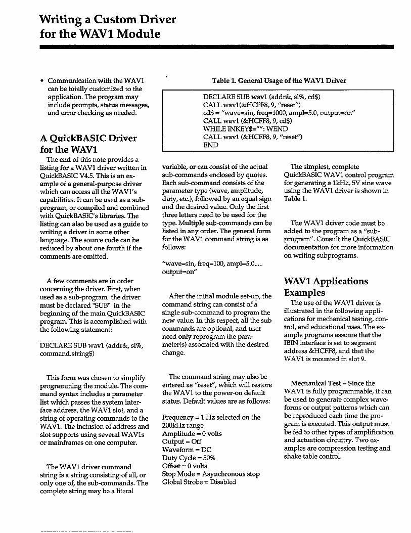
. Table 1. General Usage of the WAVl Driver
DECLARE SUB wavl (add&, sl%, cd$) CALL wavl(&HCFF8,9, “reset”) cd$ = “wave=&, freq=lOOO, ampl=5.0, output=on” CALL wavl (&HCFF8,9, cd$) WHILE INKEY$=““: WEND CALL wavl (&HCFF8,9, “reset”) END
variable, or can consist of the actual sub-commands enclosed by quotes. Each sub-command consists of the parameter type (wave, amplitude, duty, etc.), followed by an equal sign and the desired value. Only the first three letters need to be used for the type. Multiple sub-commands can be listed in any order. The general form for the WAVl command string is as follows:
Nwave=sin, freq=lOO, ampl=5.0 ,.... output=on”
After the initial module set-up, the command string can consist of a single sub-command to program the new value. In this respect, all the sub commands are optional, and user need only reprogram the para- meter(s) associated with the desired change.
The command string may also be entered as “reset”, which will restore the WAVl to the power-on default status. Default values are as follows:
Frequency = 1 Hz selected on the 2OOkHz range Amplitude = 0 volts output = Off Waveform = DC Duty Cycle = 50% Offset = 0 volts Stop Mode = Asynchronous stop Global Strobe = Disabled
The simplest, complete QuickBASIC WAVl control program for generating a lkHz, 5V sine wave using the WAVl driver is shown in Table 1.
The WAVl driver code must be added to the program as a “sub- program”. Consult the QuickBASIC documentation for more information on writing subprograms.
WAVl Applications Examples
The use of the WAVl driver is illustrated in the following appli- cations for mechanical testing, con- trol, and educational uses. The ex- ample programs assume that the IBIN interface is set to segment address &HCFF8, and that the WAVl is mounted in slot 9.
Mechanical Test - Since the WAVl is fully programmable, it can be used to generate complex wave- forms or output patterns which can be reproduced each time the pro- gram is executed. This output must be fed to other types of amplification and actuation circuitry. Two ex- amples are compression testing and shake table control.

Writing a Custom Driver for the WAVl Module
1 Figure 1. Compression Test Set-up
M Force Actuator liil
Waveform Generator
Mechanical Test i-----Et-i Series 500
l Compression Testing
l DC Offset to pre-load the sample
l Haverwave Function for smooth transition point and avoiding abrupt relaxation of the board
Table 2. Haversine Program for Compression Testing
DECLARE SUB wavl (add&, sl%, cd$) CALL wavl(&JXFF8,9, “reset/) cd$ = “wave=DC, offs=-2” CALL wavl (&HCFF8,9, cd$) T!=timer: while timer-t!<5: wend cd$ = “wave=sin, freq=l, ampl=lO, output=haver” CALL wavl(&HCFF8,9, cd$) END
Table 3. Shake Table Control Output
DECLARE SUB wavl (add&, sl%, cd$) CALL wavl(&HCFF8,9, “reset”) cd$ = “wave=square, freq=5, ampl=l, output=on” CALL wavl &HCFF8,9, cd$) t!=timerz while timer-t!<lO: wend amplt=l .o while amplt <= 5.0
cd$ = “wave=tri, freq=20, ampl=” + str$(amplt) CALL wavl(&HCFF8,9, cd$) t!=timer: while timer-t!<30: wend amplt=amplt + 0.5
wend CALL wavl (&HCFF8,9, “reset”)
For compression testing, the WAVl control registers enable the module to produce continuous waveforms, or a single pulse (haver sine or triangle) anywhere in the available range of frequency and duty cycle. This enables a variety of complex control voltages to be programmed and applied to an amplifier and force actuator. The actuator, in turn, applies a load to a sample under test. The WAVl’s offset feature makes it possible to pm-load the sample under test. A Model 500A data acquisition system can house several WAVl modules and strain gage cards. A fully integrated, multi-channel system can thus apply stimuli and monitor results.
A program which pre-loads the drive amplifier with -2.0 volts for five seconds, and then generates a 1Hz haver sine pulse with 1OV amplitude is shown in Table 2.
As a shake table controller, the WAVl can be programmed to out- put various combinations of wave- forms while amplitude, frequency, or other parameters are modulated in real time. As in the compression test example, the WAVl output must be amplified, and then applied to a voice coil or other type of actu- ator. A relatively simple computer program can call up the various WAVl waveforms, modulate the output, control wave durations, time delays, etc. This example applies the following test protocol:
1. IV, 5Hz square wave for 10 seconds
2. 2OHz triangle wave with ampli- tude increasing from 1V to 5V in .5V steps at the rate of .5V every 30 seconds.
Writing a Custom Driver for the WAVl Module
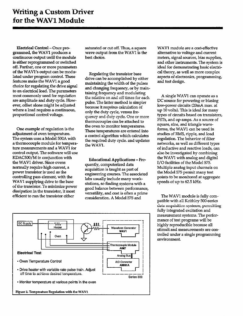
Electrical Control - Once pro- grammed, the WAVl produces a continuous output until the module is either reprogrammed or switched off. Further, one or more parameters of the WAVl’s output can be modu- lated under program control. These features make the WAVl a good choice for regulating the drive signal to an electrical load. The parameters most commonly used for regulation are amplitude and duty cycle. How- ever, offset alone might be adjusted where a load requires a continuous, proportional control voltage.
One example of regulation is the adjustment of oven temperature. The system uses a Model 500A with a thermocouple module for tempera- ture measurements and a WAVl for control output. The software will use KDAC5OO/M in conjunction with the WAVl driver. Since ovens normally require high current, a power transistor is used as the controlling pass element, with the WAVl supplying drive to the base of the transistor. To minimize power dissipation in the transistor, it most efficient to run the transistor either
saturated or cut off. Thus, a square wave output from the WAVl is the best choice.
Regulating the transistor base drive can be accomplished by either maintaining the width of the pulses and changing frequency, or by main- taining frequency and modulating the relative on and off times for each pulse. The latter method is simpler because it requires calculation of only the duty cycle, versus fre- quency and duty cycle. One or more thermocouples can be attached to the oven to monitor temperatures. These temperatures are entered into a control algorithm which calculates the required duty cycle. and updates the WAVl.
Educational Applications - Fre- quently, computerized data acquisition is taught as part of engineering courses. The associated labs usually include many work- stations, so finding systems with a good balance between performance, versatility, and cost is often a prime consideration. A Model 575 and
Waveform Generator
Electrical Tesr i Analog Bus
c
i l Oven Temperature Control A/D Converter
AMMlA
l Drive heater with variable rate pulse train. Adjust 1 off time to achieve desired temperature. L--------l
Series 500
l Monitor temperature at various points in the oven
Figure 2. Temperature Regulation with the WAVl
WAVl module are a cost-effective alternative to voltage and current meters, signal sources, bias supplies, and other instruments. The system is ideal for demonstrating basic electri- cal theory, as well as more complex aspects of electronics, programming, and test design.
A single WAVl can operate as a DC shrce for powering or biasing low-power circuits (2OmA max. at up 10 volts). This is ideal for many types of circuits based on transistors, FETs, and op-amps. As a source of square, sine, and triangle wave- forms, the WAVl can be used in studies of RMS, ripple, and load regulation. The behavior of filter networks, as well as different types of inductive and reactive loads, can also be investigated by combining the WAVl with analog and digital I/O facilities of the Model 575. Multiple analog input channels on the Model 575 permit many test points to be monitored at aggregate speeds of up to 62.5 kHz.
The WAVl module is fuhy com- patible with all Keithley 500series data acquisition systems, permitting fully integrated excitation and measurement systems. The perfor- mance of test programs will be highly reproducible because all stimuli and measurements are con- trolled under a single programming environment.
Writing a Custom Driver for the WAVl Module
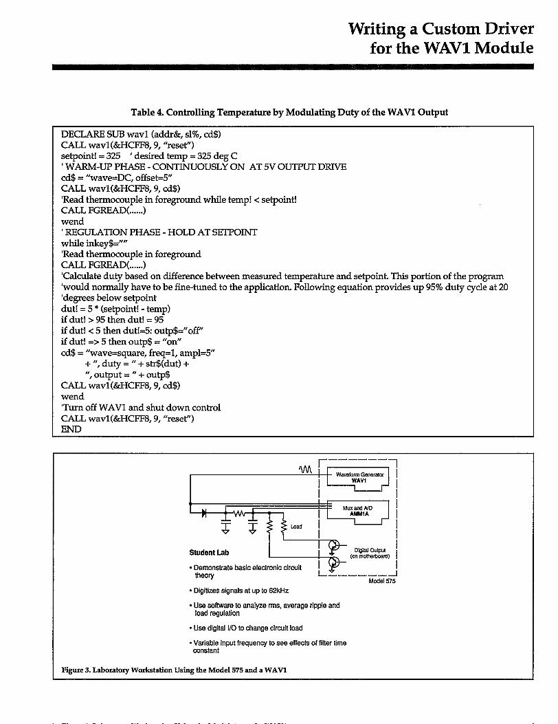
Table 4. Controlling Temperature by Modulating Duty of the WAVI Output
DECLARE SUB wavl (add&, sl%, cd$) CALL wavl(&HcFF8,9, ?eset? setpoint! = 325 ’ desired temp = 325 deg C ’ WARM-TJl? PHASE - CONTINUOUSLY ON AT 5V OTJTPUT DRIVE cd$ = “wave=DC, offset=5” CALL wavl(&HCFF8,9, cd$) ‘Read thermocouple in foreground while temp! < setpoint! CALL FGREAD(......) wend ’ REI’GULATION PHASE - HOLD AT SETPOINT while inkey$=“” ‘Read thermocouple in foreground CALL FGRFAD(......) ‘Calculate duty based on difference between measured temperature and setpoint. This portion of the program ‘would normally have to be fine-tuned to the appiication. Following equation provides up 95% duty cycle at 20 ‘degrees below setpoint dut! = 5 * (setpoint! - temp) if dut! > 95 then dut! = 95 if dut! < 5 then dut!=5: outp$=“off’ if dut! => 5 then outp$ = “on” cd$ = “wave=square, freq=l, ampl=5”
+ “, duty = fi + str$(dut) + “, output = N + outp$
CALL wavl (&HCFF8,9, cd$) wend ‘Turn off WAVl and shut down control CALL wavl(&HCFF8,9, “reset”) END
Student Lab
l Demonstrate basic electronic circuit -w ------
Model 575 l Digitizes signals at up to 62kHz
l Use software to analyze rms, average ripple and load regulation
l Use digital I/O to change circuit load
l Variable input frequency to see effects of filter time constant
Figure 3. Laboratory Workstation Using the Model 575 and a WAVl
Writing a Custom Driver for the WAVl Module
’ SUB wavl (add&, sl%, command.string$) STATIC 1 ***********************~*******~*****************************~*************************%****~***~***~**************** ’ QuickBASIC Subprogram for controlling the WAVl module.
’ (c) Keithley Instnunents, Inc. 1990 Written in Microsoft QuickBASIC 4.5 - Guy Zumpetta 3/16/90
’ Presumes that the range switch is set to 1OV position. If it is set to 1V position, output and offset amplitude will be ‘0.1 x programed value.
’ Command Syntax:
’ CALL WAVl ( address%, slot%, command-string$ )
’ Where:
’ Address - (long integer) - the segment address of the interface controlling the system containing the WAVl (e.g. ’ &zHCFF8).
’ Slot - (integer) - the slot position of the WAVl (l-10)
’ Command strings: 1
’ INIt, RESet - initialize WAVl to power-up defaults ’ FREquency = 0.1 - 200000 (Hz) ’ AMPlitude, LEVel = 0 to 10.0 (volts) ’ OUTput = Enable, Disable, Haver, or Pulse ’ WAVe = Sine, TRiangle, SQuare, or DC ’ DUTY, CYCle = 5 to 95 or .05 to .95 ’ OFFset = -10.000 to +10.000 (volts) ’ SYNC, STOpmode = Sync or Async ’ GLObal, STRobe = Enable or Disable
POWER-UP DEFAULT
1 on 2OOkHz 0 Disable DC 50 0 Async Disable
’ (Significant characters are capitalized) ’ (Some parameters have other legal aliases - see the code)
’ Include in the beginning of main program:
’ DECLARE SUB WAVl( address&, slot%, command.string$ )
’ Typical usage:
’ CALL WAVl (&HCFF8,9, “wave=sine, ampl=7.5, output=on”)
’ Up to 8 parameters can be entered as the command.string!§. The parameters must be separated by commas as shown ’ above, but can be entered in any order. If used, INIT or RESET must be used alone. After a RESet, the wave, ’ frequency, amplitude, and enable are the minimum commands to output a waveform. The other parameters wiII ’ remain at defaults.
Writing a Custom Driver for the WAVl Module
DEFINT A-Z STATIC wavt$, freq!, mg&, ampl!, duty%, offs!, outp$, stpm$, strb$ STATIC ss%, en%, fs%, gs%, rs%, ah%, al% STATIC op%, oh%, ol%, rub%, ml%, rdh%, rdl%
’ Set defaults for the parameters which may not be set through the CALL
13% = 0: mg& = 200000 IFduty%=OTHENduty%=50 IF freq! = 0 THEN freq! = 1: mg& = 200000
’ Parse the command.string$ for the knob(s)
cmd.str$ = LTRIM$(RTRIM$(LCASE$(command.string$)))
DIM wavcmds$(l2) index% = 0
FOR commapt% = 1 TO LEN(cmd.str$) IF MID$(cmd.str$, commapt%, 1) = “,” THEN
wavcmds$(index%) = LEFT$(cmd.str$, commapt% - 1) and.& = RIGHT$(cmd.str$, LEN(cmd.str$) - commapt%) cmd.str$ = LTRTM$(RTRlM$(cmd.str$r$)) index% = index% + 1 commapt% = 1
ENDIF
NEXT commapt%
wavcmds$(index%) = cmd.str$
FOR pass% = 0 TO index%
eqposn% = lNSTR(wavcmds$(pass%), “=“I op$ = LTR&@(RIGHT$(wavcmds$(pass%), (LEN(wavcmds$(pass%)> - eqposn%))) knob$ = (LEET$(wavcmds$(pass%), 3))
’ Parse elements in string array “wavcmds$(pass%)” for the operation (Ol?$)
SELECT CASE knob$ CASE “ini”, ,tres”
fs%=O ah%=O:al%=O op%=O:oh%=O:ol%=O gs%=O:ss%=O:en%=O ruh%=O:rul%=0:rdh%=O:rdl%=O duty% = 50 freq! = 1: mg& = 200000 ’ LOCATE 25,l: PRINT ‘WAVl STATUS: Initialized and ready”; GOT0 poke.values
CASE “wav” wavt$ = LEFT$(op$, 2)

Writing a Custom Driver for the WAVl Module
SELECT CASE wavt!$ CASE “dc”
fs%=O CASE “si’
fs%=l CASE “ix”
fs%=2 CASE “sq”
fS%=3 CASE ELSE
err.flag% =l GOT0 exit.wavl END SELECT
CASE “fre” Fl = VAL (op$) IF f! > 200000 OR f! < .1 THEN err.flag% = 1: GOT0 exit.wavl Ifduty%<50-f! /mg&ORduty%>lOO-50*f! /mg&THEN
err.flag% = 2 GOT0 exit.wavl
ENDIF freq! = f!
CASE “dut”, “cyc” d! =VAL (op$) if d! , 1 THEN d% = INT(100 * d!) ELSE d% = INT(d!) IFd%<5ORd%>95THEN
err.flag% = 2 GOT0 exit.wavl
ENDIF duty% = d%
CASE “amp”, “lev” a! = VAL (op$) IFa!<OORa!>lOTHFN
err.flag% = 1 GOT0 exit.wavl
ENDIF ampl! = a! bits% = (ampl! / 10) * 4095 ah% = bits% \ 256 al% = bits% MOD 256
CASE “off’ o! = VAL (op$) IFo!<-lOORo!>lOTHEN
err.flag% =1 GOT0 exit.wavl
ENDIF
op% = 0 offs! = o! IF offs! < 0 THEN op% = 1: offs! = ABS(offs!)
Writing a Custom Driver for the WAVl Module
bits% = (offs! / 10) * 4095 oh% = bits% \ 256 01% = bits% MOD 256
CASE “out” outp$ = LEF-Mop$, 2) SELECT CASE outp$
CASE “of”, “di”, “0”
en% = 0 US&- Uon”, “enlf, “1 N
en% = 1 CASE “pu”, “ha”, “2”
en% = 2 ss% = 1
CASE ELSE err.flag% = 1: GOT0 exit.wavl
END SELECT
CASE “sto”, “syn” sfp-4 = LEI=lXop$, 1) SELECT CASE stpm$
USE Ua,,, “d”, “0”
ss% = 0 &.&E I,$,, “e”, “1”
ss% = 1 CASE ELSE
err.flag% = 1: GOT0 exit.wavl END SELECT
CASE “glo”, ‘*&I” strb$ = LEFT$(op$, 1) SELECT CASE strb$
(-ME “d”, “0”
gs%=O CA% “e”, “1”
gs%=l CASE ELSE
err.flag% = 1: GOT0 exit.wavl END SELECT
CASE ELSE emflag% = 1: GOT0 exit.wavl
END SELECT NEXT pass%
’ Select range bits based on desired input freq IF freq! <= 200000 THFN rs% = 0: mg& = 200000 IF freq! <= 20000 THEN r-s% = 1: mg& = 20000 IF freq! <= 2000 THEN rs% = 2: mg& = 2000 lJ?freq!<=2OOTHENrs%=3:mg&=200 IFfreq!<=20THENrs%=4:mg&=20 IFfreq!<=2THENrs%=5:mg&=2
Writing a Custom Driver for the WAVl Module
calc.ramps: ru.bits& = INTJ(freq! * 2 * 11 - 1) / (m&z * (1 - (dutv% / 100)))) rd.bits& = INT((freq! * 2 A 11 - 1) / (m& * (duty% 1 100)))
’ See if either ramp exceeds 4095 and toggle up one range if necessary
IF (mbits& > 4095 OR rd.bits& > 4095) THEN mg& = mg& * 10 IS% = rs% - 1 GOT0 calc.ramps
INDIF
’ Check again that the range select and total ramp up/down values are legal
IF r-s% < 0 THEN err.flag% = 3: GOT0 exit.wavl IF mbits& > 4095 THEN mbits% = 4095: err.flag% = 2 IF rd.bits& > 4095 THEN rd.bits% = 4095: err.flag% = 2
‘Set up the high nibbles and low bytes only if no errors have been detected
rub% = mbits& \ 256 ml% = mbits& MOD 256
rdh% = rd.bits& \ 256 rdl% = rd.bits& MOD 256
poke.values:
‘Set up CMDA and CMDB and POKE out the information
DBF SEG = add& cmnd.a& = 2 * (~1% - 1) annd.b& = annd.a& + 1
POKE cmnd.a&, (7 * 32) + rdh% POKE annd.b&, rdl%
POKE annd.a&, (6 * 32) + rub% POKE annd.b&, ml%
POKE annd.a&, (5 * 32) + (op% * 16) + oh% POKE cmnd.b&, 01%
POKE cmnd.a&, (4 * 32) + ah% POKE cmnd.b&, al%
POKE cmnd.a&, (1% 32) + gs% * 8 + rs%
IFen%=OORen%=lTHEN POKE cmnd.a&, (0 * 32) + (ss% + 8) + (en% * 4) + fs%
Writing a Custom Driver for the WAVI Module
ELSEIF en% = 2 THEN POKE cmnd.a&, (0 * 32) + (ss% * 8) + (0) + fs% POKE cmnd.a&, (0 * 32) + (ss% * 8) + (4) + fs% POKE cmnd.a&, (0 * 32) + (ss% * 8) + (0) + fs%
ENDIF
exit.wavl :
IF err.flag% = 1 THEN SOUND 1000,l LOCATE 25,1 PRINT “ERROR 1: WAVl function “‘; wavcmds$(t%); ,,’ is illegal or out of limits “;
ENDIF
IF err.flag% = 2 THEN SOUND 1000,l LOCATE 25,1 PRINT “ERROR 2: Frequency “‘; f!; ,,’ out of limits for duty cycle “‘; duty%; ,,’ “;
ENDIF
IF err.flag% = 3 THEN SOUND 1000,l LOCATE 25,1 PRINT “ERROR 3: Frequency “‘; freq!; “’ out of limits for duty cycle “‘; duty%; II’ “;
EN-DIF
err.flag% = 0
’ DEF SEG back to 20 (or appropriate value if Keithley software is not used).
ERASE wavcmds$ DEF SEG = 20
ENDSUB
Writing a Custom Driver for the WAVl Module
Data Acquisition and Control Division
Keithley Instruments, Inc. l 28775 Aurora Road l Cleveland, Ohio 44139 l (216) 248-0400 l Fax: 349-4569 WEST GERMANY: Keithley Instruments GmbH l Heiglhofstr. 5 l Miinchen 70 l 089-71002-O l Telex: 52-12160 l Fax: 089-7100259 GREAT BRITAIN: Keithley Instruments, Ltd. l 1 Boulton Road l Reading, Berkshire RG 2 ONL l 0734-861287 l Telex: 847 047 l Fax: 0734-863665 FRANCE Keithley Instruments SARL 03 All& des Garays0B.P. 60 l 91124 Palatseau/Z.I. * l-6-0115 155 *Telex: 600 933aFax: l-6-0117726 NETHERLANDS: Keithley Instruments BV* Avelingen West 49 04202 MS Gorinchem*P.O. Box 559.4200 AN Goxinchem*01830-35333eTelex: 24 684 l Fax: 01830-308~. SWITZERLAND: Keithley Instruments SA l Kriesbachstr. 4 l 8600 Diibendorf l 01-821-9444 l Telex: 828 472 0 Fax: 0222-315366 AUSTRIA: Keithley Instruments GesmbH l Rosenhtigelstrasse 12 l A-1120 Vienna l (0222) &) 65 48 l Telex: 131677 l Fax: (0222) 84 35 97 ITALY: Keithley Instruments SRL l Viale S. Giignano 4/A l 20146 Milan0 l 024120360 or 02-4156540 l Fax: 02-4121249