
Water Jet Guided Laser Cutting of Silicon Thin Films Using ... · Water Jet Guided Laser Cutting of...
6
JLMN-Journal of Laser Micro/Nanoengineering Vol. 6, No. 2, 2011 168 Water Jet Guided Laser Cutting of Silicon Thin Films Using 515nm Disk Laser Eva-Maria Heilmann * , Albrecht Seidl ** and Ralf Hellmann * * University of Applied Sciences Aschaffenburg, Wuerzburger Strasse 45, D-63743 Aschaffenburg E-mail: [email protected] ** Schott Solar Wafer GmbH, Carl-Zeiss-Strasse 4, D-63755 Alzenau We report on a comprehensive study of water jet guided laser cutting of polycrystalline silicon thin films using a pulsed 515nm disk laser. The optimization of the cutting process of polycrystalline sil- icon wafers having a thickness of 200-300µm is based on a Design of Experiments (DOE) approach taking into account process parameters such as laser power, cutting speed, laser repetition rate, wa- ter pressure and nozzle diameter, respectively. The targeted response of the DOE is defined by both the quality as well as the productivity of the cutting process. While the former is measured by the mechanical strength and the chipping of the wafers, the latter is determined by the ablation depth and the cutting kerf cross-sectional area. Our analysis identifies the most influencing parameters on the cutting process, provides insight into the interactions of these parameters and, finally, delivers an optimized process parameter window for water jet guided laser cutting of thin silicon films. Keywords: water jet guided laser cutting, silicon thin film, Design of Experiment, disk laser 1. Introduction Water jet guided laser cutting using pulsed lasers has re- cently attracted considerable interest [1-5]. This technology is associated to valuable advantages in laser micromachin- ing as compared to the conventional dry laser based cutting processes with coaxial gas assist. These advantages are, e.g., a significantly reduced heat affected zone due to the cooling of the interaction zone by the continuous water jet in between the laser pulses, an efficient removal of molten material by the water jet, reduced surface contamination by debris, highly parallel kerf walls, and a large working dis- tance determined by the stable laminar water jet, respec- tively [3,6]. The latter, in turn, eliminates the need of any focus control that is typically needed in dry laser cutting to hold the relative position of the focal point and the work piece within the Rayleigh length of the laser source. These advantages have been proven to lead to an excellent cutting quality [7,8]. Using pulsed diode pumped solid state lasers the potential of water jet guided laser cutting has been demonstrated for various materials and applications, such as cutting and grooving of silicon, gallium arsenide and silicon carbide wafers [6,9,10], cutting of thin stainless steel sheets [1], copper foils and polyimide films with cupper plating [6,10], and scribing of low temperature co-fired ceramics [10,11]. From a market point of view, these applications adress in- dustrial fields such as the semiconductor and electronics industry (e.g. the solar cell and high brightness LED mar- ket), the medical, tooling and the watch industry, respec- tively [1-3,10]. The cited reports, however, focus on the demonstration of the successful implementation of the technology and do not detail any optimization of the pro- cess. Here, we report on a comprehensive study of water jet guided laser cutting of polycrystalline silicon thin films having a thickness of 200-300µm. Similar as the above mentioned applications the cutting process of silicon thin films is governed by the laser while the water jet is respon- sible for the material removal out of the cutting kerf and of its cooling. Please note that in our experiments the water jet produces only a mechanical strength of 0.17N. The optimi- zation of the cutting process is based on a DOE approach. The response of the DOE is well defined by the quality and productivity of the cutting process. The former is quantita- tively determined by the mechanical strength and the chip- ping of the silicon wafers and the latter is measured by the ablation depth and the cross-sectional area of the cutting kerf. Within the DOE approach we take into account the most influencing cutting parameters such as laser power, cutting speed, laser repetition rate, water pressure and nozzle di- ameter, respectively. As a result, we identify an optimized parameter window with regard to the targeted response (quality and productivity). 2. Experimental 2.1 Polycrystalline wafers The polycristalline silicon wafers have been produced by the edge-defined film-fed growth technology (EFG). De- tails of this technology have been published by the authors and others [12,13]. Using EFG, up to seven meter long, thin (200-300µm) octagonal or dodecagonal silicon tubes can be produced. Out of each side of the polygonal tube a 125x125mm 2 square wafer is laser cut and further pro- cessed to a solar cell. To maintain a sufficient quality of the cutting edges, usually a multiple pass cutting process is required. Technical Communication
-
Upload
nguyenkhanh -
Category
Documents
-
view
224 -
download
0
Transcript of Water Jet Guided Laser Cutting of Silicon Thin Films Using ... · Water Jet Guided Laser Cutting of...
JLMN-Journal of Laser Micro/Nanoengineering Vol. 6, No. 2, 2011
168
Water Jet Guided Laser Cutting of Silicon Thin Films Using 515nm Disk Laser
Eva-Maria Heilmann*, Albrecht Seidl** and Ralf Hellmann*
*University of Applied Sciences Aschaffenburg, Wuerzburger Strasse 45, D-63743 Aschaffenburg E-mail: [email protected]
** Schott Solar Wafer GmbH, Carl-Zeiss-Strasse 4, D-63755 Alzenau
We report on a comprehensive study of water jet guided laser cutting of polycrystalline silicon thin films using a pulsed 515nm disk laser. The optimization of the cutting process of polycrystalline sil-icon wafers having a thickness of 200-300µm is based on a Design of Experiments (DOE) approach taking into account process parameters such as laser power, cutting speed, laser repetition rate, wa-ter pressure and nozzle diameter, respectively. The targeted response of the DOE is defined by both the quality as well as the productivity of the cutting process. While the former is measured by the mechanical strength and the chipping of the wafers, the latter is determined by the ablation depth and the cutting kerf cross-sectional area. Our analysis identifies the most influencing parameters on the cutting process, provides insight into the interactions of these parameters and, finally, delivers an optimized process parameter window for water jet guided laser cutting of thin silicon films.
Keywords: water jet guided laser cutting, silicon thin film, Design of Experiment, disk laser
1. Introduction Water jet guided laser cutting using pulsed lasers has re-cently attracted considerable interest [1-5]. This technology is associated to valuable advantages in laser micromachin-ing as compared to the conventional dry laser based cutting processes with coaxial gas assist. These advantages are, e.g., a significantly reduced heat affected zone due to the cooling of the interaction zone by the continuous water jet in between the laser pulses, an efficient removal of molten material by the water jet, reduced surface contamination by debris, highly parallel kerf walls, and a large working dis-tance determined by the stable laminar water jet, respec-tively [3,6]. The latter, in turn, eliminates the need of any focus control that is typically needed in dry laser cutting to hold the relative position of the focal point and the work piece within the Rayleigh length of the laser source. These advantages have been proven to lead to an excellent cutting quality [7,8]. Using pulsed diode pumped solid state lasers the potential of water jet guided laser cutting has been demonstrated for various materials and applications, such as cutting and grooving of silicon, gallium arsenide and silicon carbide wafers [6,9,10], cutting of thin stainless steel sheets [1], copper foils and polyimide films with cupper plating [6,10], and scribing of low temperature co-fired ceramics [10,11]. From a market point of view, these applications adress in-dustrial fields such as the semiconductor and electronics industry (e.g. the solar cell and high brightness LED mar-ket), the medical, tooling and the watch industry, respec-tively [1-3,10]. The cited reports, however, focus on the demonstration of the successful implementation of the technology and do not detail any optimization of the pro-cess. Here, we report on a comprehensive study of water jet guided laser cutting of polycrystalline silicon thin films
having a thickness of 200-300µm. Similar as the above mentioned applications the cutting process of silicon thin films is governed by the laser while the water jet is respon-sible for the material removal out of the cutting kerf and of its cooling. Please note that in our experiments the water jet produces only a mechanical strength of 0.17N. The optimi-zation of the cutting process is based on a DOE approach. The response of the DOE is well defined by the quality and productivity of the cutting process. The former is quantita-tively determined by the mechanical strength and the chip-ping of the silicon wafers and the latter is measured by the ablation depth and the cross-sectional area of the cutting kerf. Within the DOE approach we take into account the most influencing cutting parameters such as laser power, cutting speed, laser repetition rate, water pressure and nozzle di-ameter, respectively. As a result, we identify an optimized parameter window with regard to the targeted response (quality and productivity). 2. Experimental
2.1 Polycrystalline wafers
The polycristalline silicon wafers have been produced by the edge-defined film-fed growth technology (EFG). De-tails of this technology have been published by the authors and others [12,13]. Using EFG, up to seven meter long, thin (200-300µm) octagonal or dodecagonal silicon tubes can be produced. Out of each side of the polygonal tube a 125x125mm2 square wafer is laser cut and further pro-cessed to a solar cell. To maintain a sufficient quality of the cutting edges, usually a multiple pass cutting process is required.
Technical Communication
Hiromi
タイプライターテキスト
DOI:10.2961/jlmn.2011.02.0013
JLMN-Journal of Laser Micro/Nanoengineering Vol. 6, No. 2, 2011
169
2.2 Laser system Throughout our study we used a commercial water jet guided laser cutting system (Synova Microjet®) equipped with a fiber coupled 515nm pulsed disk laser delivering an averaged output power of 400W at 100kHz (Trumpf Tru-Micro 7250). The principle of water jet guided laser cutting has been published in Ref. [1,14,15]. As the absorption in water is lowest around 500nm, using a laser in this spectral range is advantageous. In addition, the absorption in silicon is considerably higher by several orders of magnitude in this spectral range as compared to the near infrared (the spectral range of the fundamental emission of solid state lasers) [16]. Own power measurements revealed fiber losses of about 10% and additional lossed by the optical head of the cutting system and the water jet of about 20%. Hence about 70% of the laser delivered power is available for laser cutting.
2.3 Design of Experiment (DOE) For the DOE a commercially available software package (JMP® by SAS) was employed. The relevant parameters used in the optimization process are summarized in Table 1, which define the input parameters for the DOE. To get ac-quainted with the process, the DOE consists initially of a Screening Design, based on which the most influencing parameters on the response are identified. Subsequently, within a Response Surface Design possible interactions between diffeent parameters are examined and the opti-mized parameter sets are determined. Finally, the calculat-ed optima are further examined with regard of the opti-mized quality and productivity (response).
2.4 Responses 2.4.1 Quality
The cutting quality in our study is defined firstly by the mechanical strength of the wafers and secondly by the chipping at the backside of the laser cut wafers. The me-chanical strength of the wafers is of crucial importance with respect to subsequent process steps of the wafer with-in the solar cell manufacturing. As the laser based cutting process is a thermal process, the thermal stress although reduced by the water jet results in mechanical strain lead-ing to microcracks in polycrystalline silicon. The generated micro-cracks in turn lead to a reduction of the mechanical breaking strength, which is tested by a four-bar-bending test [12]. In this test, the thin silicon film is strained by compression. The pressure is caused by four parallel bars. A schematic design is shown in Figure 1.
Fig. 1 Four-bar-bending test [12]
Chipping refers to material outbreaks at the wafer backside along the cut kerf. To quantitatively assess the chipping, the wafer backside is illuminated and the brightness maxima of the reflection resulting from the chipping are counted using a photo editor. Lower chipping refers to higher quality of the cut kerf.
2.4.2 Productivity From a productivity point of view, the effective cutting speed and the ablation efficiency are of interest. Both pa-rameters can be calculated by measuring the ablation depth and the kerf cross-sectional area. The theoretical effective cutting speed is given by
dvAveff⋅
= (1),
with the ablation depth A, the velocity v, and the wafer thickness d, respectively. The ablation depth describes the average depth T of the first three passes (p).
pTA = (2)
The ablation efficiency can be calculated by [17]:
Siex
Sith
HH
,
,
∆
∆=h (3)
The formula describes the ratio of the theoretical energy required to melt 1mm3 of silicon (ΔHth,Si) and the experi-mental ablation efficiency ΔHex,Si. The latter is composed of laser power P, velocity v, kerf cross-sectional area Agr and the absorption coefficient α of silicon at the laser wave-length. For polycrystalline silicon ΔHth,Si is 50J/mm3 [17] and ΔHex,Si can be experimentally determined according:
vAPH
grSiex
α=∆ ,
(4)
Using these values in our study, h is calculated and used to evaluate the efficiency of the cutting process.
3. Results and Discussion
3.1 Screening Design (SD) To get acquainted with the investigated process, the DOE starts with a SD. As the cutting process is governed by a large number of influencing parameters, the SD also serves to separate those variables with major influence from those
Table 1 Input parameter
Parameter Range Unit Wavelength 515 nm Power (max.) 35-400 W Power water jet 25-275 W Repetition rate 5-100 kHz Water pressure 100-500 bar Nozzle diameter 60, 80, 100 µm Velocity 10-500 mm/s
JLMN-Journal of Laser Micro/Nanoengineering Vol. 6, No. 2, 2011
170
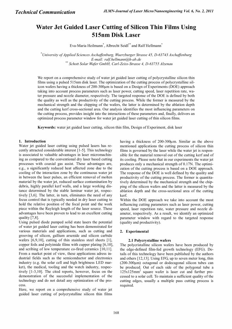
with minor influence on the response. The latter can then be kept constant during the forthcoming study, i.e. the Re-sponse Surface Design (RSD) [18]. To evaluate the influence of the parameters given in Table 2 and to determine the limits of these parameters with respect to a feasible process, we have examined a se-ries of laser cuts in the parameter range given in Table 2 (Screening Design). As a result, the parameter range is re-duced to those values that will be further used in the RSD (Table 2). In our experiments it turns out that the nozzle of the water jet laser system, particularly for smaller nozzle diameters, is sensitive to high laser powers, resulting in nozzle cracks. In addition, as shown in Figure 2 at higher laser powers we observe instabilities of the cutting process and a significant heat affected zone, due to an insufficient cooling rate at power levels beyond 100W. As a result of our analysis, we therefore limit the maximum laser power for the RSD to 100W and the nozzle diameter to 80µm, as the later leads to the highest values of the breaking strength.
Fig. 2 Instability of the cutting process and heat affected zone at 150W laser output power.
Furthermore, the SD reveals that a water pressure of about 330bar leads to wafer damages, e.g. broken wafers or mi-crocracks. Hence, in the RSD the water pressure is evaluat-ed only in a range between 100-330bar. As the pulse energy and pulse duration decrease with in-creasing repetition rate, we find within the SD that efficient material separation is starting at 50W at a repetition rate of 55kHz. At maximum repetition rate (100kHz) a minimum laser output power of 70W is required. To guarantee an efficient material separation, the cutting velocity should not fall below 100mm/s. For lower veloci-ties, the process stops almost completely, which might be attributed to a deformation of the water jet impinging onto the steeper cutting edge at lower cutting velocities. Table 2 summarizes the parameter ranges examined in the SD and those used in the forthcoming RSD. In total the SD encompassed 21 individual experiments to identify the in-fluence of the examined parameters and to limit the param-eter range.
3.2 Response Surface Design (RSD) Based on the results of the SD, the DOE is extended to a RSD by ten further experiments to identify possible quad-ratic dependencies. The parameter ranges for the RSD are also shown in Table 2, which includes the factors laser out-put power, repetition rate, water pressure, nozzle diameter and velocity. The parameter levels are illustrated in Table 3.
The objective is to determine the optimized parameter sets for both quality and productivity, respectively.
3.2.1 Productivity measurements
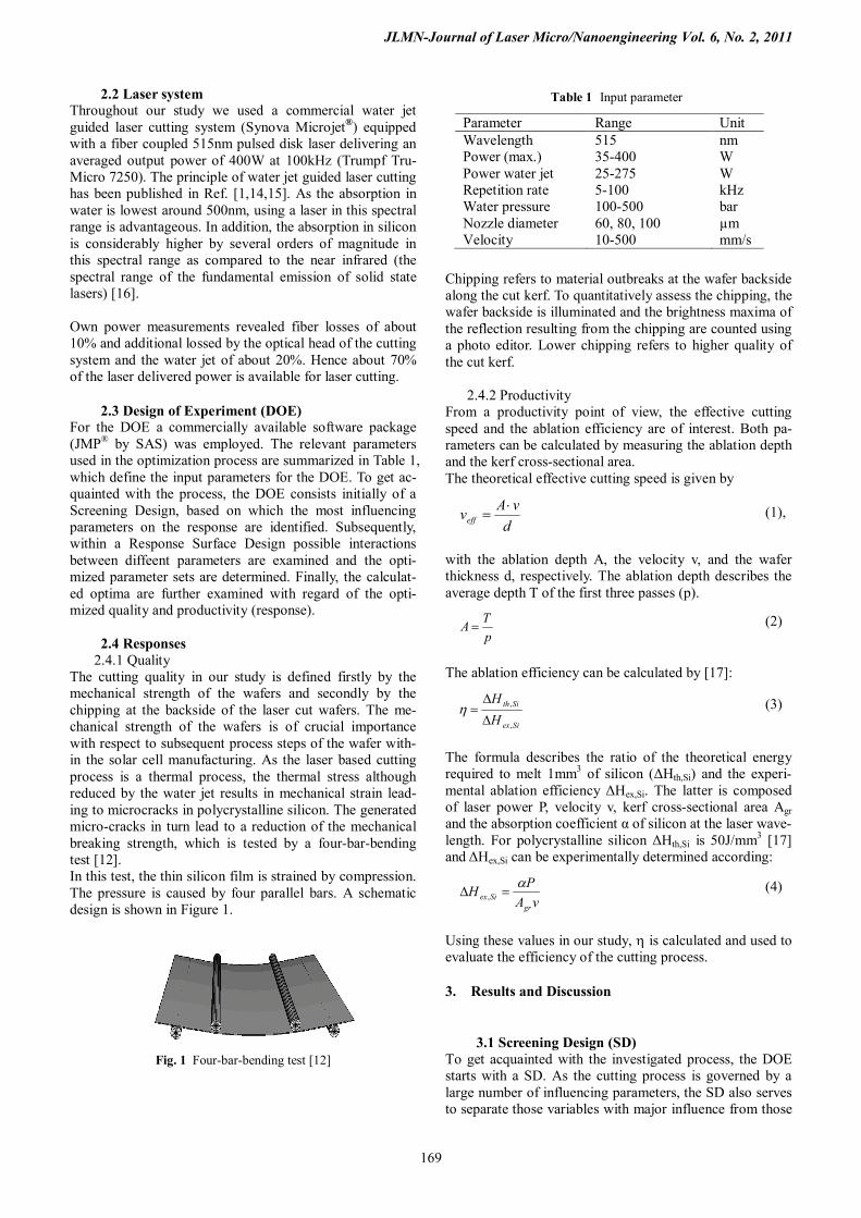
In order to achieve high operational throughputs, the effec-tive cutting speed and the ablation efficiency are deter-mined during the RSD by measuring the ablation depth and the kerf cross-sectional area for a series of laser cuts. A typical cut kerf (single pass) as measured with a digital microscope is illustrated in Figure 4. Here, the kerf width
as determined at the top of the kerf is 76.4µm. Throughout our study we found that the kerf width decreases with in-creasing repetition rate. At 100kHz it is comparable to the used nozzle diameter of 80µm and at 10kHz the kerf width is about 160µm. In addition, lower repetition rates lead to significant heat affected zones due to high pulse energies. Therefore, we limit the repetition rate in the range between 55kHz and 100kHz.
Fig 4 Digital microscope illustration of a cut kerf (single pass) at 215bar water pressure, 71,7W laser output power, 100kHz repeti-
tion rate and 200mm/s velocity. The width of the v-shaped cut kerf is about 76.4µm at its top.
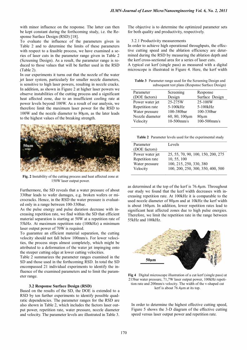
In order to determine the highest effective cutting speed, Figure 5 shows the 3-D diagram of the effective cutting speed versus laser output power and repetition rate.
Table 3 Parameter range used for the Screening Design and subsequent test plans (Response Surface Design)
Parameter (DOE factors)
Screening Design
Response Surface Design
Power water jet 25-275W 25-100W Repetition rate 5-100kHz 5-100kHz Water pressure 100-380bar 100-330bar Nozzle diameter 60, 80, 100µm 80µm Velocity 10-500mm/s 100-500mm/s
Table 2 Parameter levels used for the experimental study
Parameter (DOE factors)
Levels
Power water jet 25, 55, 70, 90, 100, 150, 200, 275 Repetition rate 10, 55, 100 Water pressure 100, 215, 250, 330, 380 Velocity 100, 200, 250, 300, 350, 400, 500
50µm
50µm
JLMN-Journal of Laser Micro/Nanoengineering Vol. 6, No. 2, 2011
171
Generally, 3-D diagrams serve to visualize the response (e.g. effective cutting speed or ablation efficiency) as a function of two parameters, while the remaining parame-ters are kept constant. Thus, interactions between two pa-rameters are investigated. For this analysis the cutting ve-locity was pre-set to 500mm/s.
Fig. 5 3-D simulation of the effective cutting velocity as a func-tion of laser output power and repetition rate (pre-set cutting ve-
locity of 500mm/s).
A contour diagram as shown in Figure 6 is derived from the 3D-diagram, in which each line corresponds to a cut through the surface of the 3D-plot.
20
40
60
80
10
Rep
etiti
on ra
te [k
Hz]
Effective cutting speed [mm/s]
20
50
80
110
140
170
20 40 60 80 100 120
Power [W] Fig. 6 Preferable effective cutting speed about 100mm/s (marked area) versus laser output power, repetition rate and a pre-set cut-
ting velocity of 500mm/s.
The green highlighted area in Figure 6 illustrates the pa-rameter regime of laser output power and repetition rate to obtain a calculated effective cutting speed of at least
100mm/s. Based on large wall thickness variations pro-duced from the EFG procedure and the subsequent increase of passes, in practice an effective cutting speed of 75mm/s is desirable. Hence, a theoretical effective cutting speed of 100mm/s should be achieved. Taking into account the above described power limitations to 100W, Figure 6 re-veals that moderate powers of 50 to 100W and mean repeti-tion rates lead to preferable effective cutting speeds. Based on our measurements of the cross sectional areas of the cutting kerf, we have determined the ablation efficiency h by measuring ΔHex,Si acccording Formula 3 and 4. The results are shown in Figure 7 for different parameter com-binations in the velocity range between 100 and 500mm/s and repetition rates up to 100kHz. We found maximum ablation efficiencies at 55kHz repetition (determined at 60 to 90W) and, by trend, at cutting velocities up to 300mm/s. However, with increasing cutting velocity about 300mm/s we observe a decreasing ablation efficiency.
Fig 7 Ablation efficiency as a function of velocity grouped by
repetition rate. Maximum ablation efficiency at 55kHz and 300mm/s for a given laser power regime.
Concluding the first part of the RSD, main influencing pa-rameters are laser output power, cutting velocity and repeti-tion rate. Highest productivity can be achieved at 80W laser output power, 55kHz repetition rate and 300mm/s cutting speed.
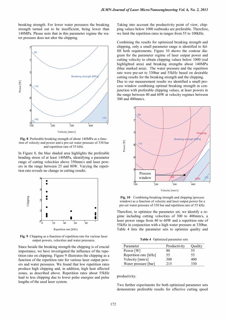
3.2.2 Quality measurements To analyse the quality of the cutting process, we have de-termined the breaking strength of the wafers and the chip-ping at the backside of the wafers. The results of the corresponding RSD are shown in the contour plots 8 and 10, respectively, which have been de-rived from the 3D-plots as described above. Figure 8 shows the contours of the breaking strength versus laser power and velocity at a water pressure of 330bar and a repetition rate of 55kHz. In general the function of the water jet is similar to a conventional gas jet. The higher the pressure the better is the removal of the molten material. In this case a high water pressure of 330bar leads to high
JLMN-Journal of Laser Micro/Nanoengineering Vol. 6, No. 2, 2011
172
breaking strength. For lower water pressures the breaking strength turned out to be insufficient, being lower than 140MPa. Please note that in this parameter regime the wa-ter pressure does not alter the chipping.
20
40
60
80
10
12
14
Pow
er [W
]
Breaking strength [MPa]
140
110
80
170
100 200 300 400 5
Velocity [mm/s]
Fig. 8 Preferable breaking strength of about 140MPa as a func-tion of velocity and power and a pre-set water pressure of 330 bar
and repetition rate of 55 kHz.
In Figure 8, the blue shaded area highlights the preferable bending stress of at least 140MPa, identifying a parameter range of cutting velocities above 350mm/s and laser pow-ers in the range between 25 and 80W. Varying the repeti-tion rate reveals no change in cutting results.
0
10
20
30
40
Chi
ppin
g
0 20 40 60 80
Repetition rate [kHz] Fig. 9 Chipping as a function of repetition rate for various laser
output powers, velocities and water pressures.
Since beside the breaking strength the chipping is of crucial importance, we have investigated the influence of the repe-tition rate on chipping. Figure 9 illustrates the chipping as a function of the repetition rate for various laser output pow-ers and water pressures. We found that low repetition rates produce high chipping and, in addition, high heat affected zones, as described above. Repetition rates about 55kHz lead to less chipping due to lower pulse energies and pulse lengths of the used laser system.
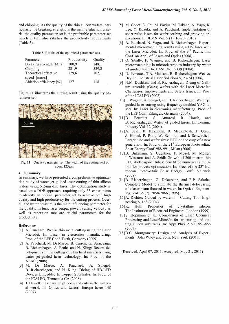
Taking into account the productivity point of view, chip-ping values below 1000 outbreaks are preferable. Therefore, we limit the repetition rates in ranges from 55 to 100kHz. Combining the results for optimized breaking strength and chipping, only a small parameter range is identified to ful-fill both requirements. Figure 10 shows the contour dia-gram for the parameter regime of laser output power and cutting velocity to obtain chipping values below 1000 (red highlighted area) and breaking strengths about 140MPa (blue marked area). The water pressure and the repetition rate were pre-set to 330bar and 55kHz based on desirable cutting results for the breaking strength and the chipping. Due to our measurement results we identified a small pro-cess window combining optimal breaking strength in con-junction with preferable chipping values, at laser powers in the range between 40 and 60W at velocity regimes between 300 and 400mm/s.
20
40
60
80
10
12
14
Pow
er [W
]
Chipping
Breaking strength [MPa]
140
110
80
170200 700 1200
100 200 300 400 5
Velocity [mm/s] Fig. 10 Combining breaking strength and chipping (process window) as a function of velocity and laser output power for a pre-set water pressure of 330 bar and repetition rate of 55 kHz.
Therefore, to optimize the parameter set, we identify a re-gime including cutting velocities of 300 to 400mm/s, a laser power range from 40 to 60W and a repetition rate of 55kHz in conjunction with a high water pressure at 330bar. Table 4 lists the parameter sets to optimize quality and
productivity. Two further experiments for both optimized parameter sets demonstrate preferable results for effective cutting speed
Table 4 Optimized parameter sets
Parameter Productivity Quality Power [W] 80 55 Repetition rate [kHz] 55 55 Velocity [mm/s] 300 400 Water pressure [bar] 215 330
Process window
JLMN-Journal of Laser Micro/Nanoengineering Vol. 6, No. 2, 2011
173
and chipping. As the quality of the thin silicon wafers, par-ticularly the breaking strength, is the main evaluation crite-ria, the quality parameter set is the preferable parameter set, which in turn also satisfies the productivity requirements (Table 5).
Figure 11 illustrates the cutting result using the quality pa-rameter set.
Fig. 11 Quality parameter set. The width of the cutting kerf of
about 125µm.
4. Summary In summary, we have presented a comprehensive optimiza-tion study of water jet guided laser cutting of thin silicon wafers using 515nm disc laser. The optimization study is based on a DOE approach, requiring only 33 experiments to identify an optimal parameter set to achieve both high quality and high productivity for the cutting process. Over-all, the water pressure is the main influencing parameter for the quality. In turn, laser output power, cutting velocity as well as repetition rate are crucial parameters for the productivity. References [1] A. Pauchard: Precise thin metal cutting using the Laser
MicroJet. In: Laser in electronics manufacturing, Proc. of the LEF Conf. Fürth, Germany (2009).
[2] A. Pauchard, M. Di Marco, B. Carron, G. Suruceanu, B. Richerzhagen, A. Brulé, and N. Kling: Recent de-velopments in the cutting of ultra hard materials using water jet-guided laser technology. In: Proc. of the ALAC (2008).
[3] M. Di Marco, A. Pauchard, A. Spiegel, B. Richerzhagen, and N. Kling: Dicing of HB-LED Devices Embedded In Copper Substrates. In: Proc. of the ICALEO, Tennecula CA (2008).
[4] J. Hewett: Laser water jet cools and cuts in the materi-al world. In: Optics and Lasers, Europe Issue 148 (2007).
[5] M. Gobet, S. Obi, M. Pavius, M. Takano, N. Vago, K. Lee, Y. Kozuki, and A. Pauchard: Implementation of short pulse lasers for wafer scribing and grooving ap-plications. In: JLMN Vol. 5 (1), 16-20 (2010).
[6] A. Pauchard, N. Vago, and B. Richerzhagen: Experi-mental micromachining results using a UV laser with the Laser MicroJet. In: Proc. of the 3rd Pacific Int. Conf. on Appl. of Lasers and Optics (2008).
[7] O. Sibally, F. Wagner, and B. Richerzhagen: Laser micromachining in microelectronics industry by water jet guided laser. In: LASE Vol. 5339 (2004).
[8] D. Perrottet, T.A. Mai, and B. Richerzhagen: Wet vs. Dry. In: Industrial Laser Solutions 5, 23-24 (2006).
[9] N.M. Dushkina and B. Richerzhagen: Dicing of Galli-um Arsenide (GaAs) wafers with the Laser MicroJet: Challenges, Improvements and Safety Issues. In: Proc. of the ICALEO (2002).
[10] F. Wagner, A. Spiegel, and B. Richerzhagen: Water jet guided laser cutting using frequency doubled YAG la-sers. In: Laser in electronics manufacturing, Proc. of the LEF Conf. Erlangen, Germany (2004).
[11] D. Perrottet, S. Amorosi, R. Housh, and B. Richerzhagen: Water jet guided lasers. In: Ceramic Industry Vol. 12 (2004).
[12] A. Seidl, B. Birkmann, B. Mackintosh, T. Grahl, J. Horzel, P. Roth, W. Schmidt, and I. Schwirtlich: Larger tube and wafer sizes: EFG on the cusp of a new generation. In: Proc. of the 21st European Photovoltaic Solar Energy Conf. 988-991, Milan (2006).
[13] B. Birkmann, S. Guenther, F. Mosel, M. Müller, I. Westram, and A. Seidl: Growth of 200 micron thin EFG dodecagonal tubes: benefit of numerical simula-tion for process optimization. In: Proc. of the 23rd Eu-ropean Photovoltaic Solar Energy Conf., Valencia (2008).
[14] B. Richerzhagen, G. Delacrétaz, and R.P. Salathé: Complete Model to simulate the thermal defocussing of a laser beam focused in water. In: Optical Engineer-ing, Vol. 35 (7), 2058-2066 (1996).
[15] A. Richter: Guided by water. In: Cutting Tool Engi-neering 8, 168 (2004).
[16] R. Hull: Properties of crystalline silicon. The Institution of Electrical Engineers. London (1999).
[17] S. Hopmann et al.: Comparison of Laser Chemical Processing and LaserMicroJet for structuring and cut-ting silicon substrates. In: Appl Phys A 95, 857-866 (2009).
[18] D.C. Montgomery: Design and Analysis of Experi-ments. John Wiley and Sons. New York (2001).
Table 5 Results of the optimized parameter sets
Parameter Productivity Quality Breaking strength [MPa] 100,9 148,1 Chipping 221,9 539,2 Theoretical effective speed [mm/s]
129,6 102,1
Ablation efficiency [%] 127 118
50µm
(Received: April 07, 2011, Accepted: May 21, 2011)