
VTT Silicon photonics · Silicon photonics foundry services at VTT Timo Aalto VTT Technical...
47
Silicon photonics foundry services at VTT Timo Aalto VTT Technical Research Centre of Finland [email protected] PIC Training, Santa Clara, 17th Nov 2016
Transcript of VTT Silicon photonics · Silicon photonics foundry services at VTT Timo Aalto VTT Technical...
Silicon photonics foundry
services at VTT
Timo Aalto
VTT Technical Research Centre of Finland
PIC Training, Santa Clara, 17th Nov 2016

22
Outline
What does ”Thick SOI” or ”Micron-scale silicon photonics” mean?
Introduction to VTT and its Micronova fab
Basics of rib and strip waveguides in Thick-SOI
Shrinking the bend size
The 3 µm SOI platform: Basic building blocks and advanced PICs
The 12 µm SOI platform: A photonic motherboard
Design support and access in Thick-SOI
Application examples
Conclusions
44
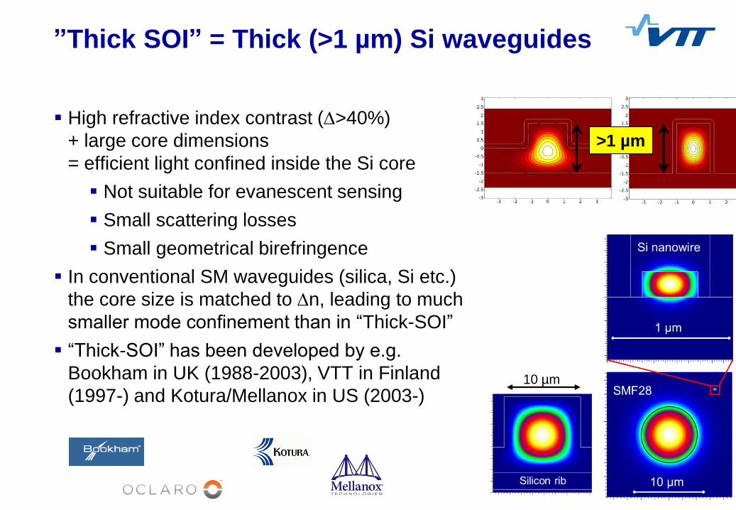
”Thick SOI” = Thick (>1 µm) Si waveguides
High refractive index contrast (>40%)
+ large core dimensions
= efficient light confined inside the Si core
Not suitable for evanescent sensing
Small scattering losses
Small geometrical birefringence
In conventional SM waveguides (silica, Si etc.)
the core size is matched to n, leading to much
smaller mode confinement than in “Thick-SOI”
“Thick-SOI” has been developed by e.g.
Bookham in UK (1988-2003), VTT in Finland
(1997-) and Kotura/Mellanox in US (2003-)
>1 µm
10 µm

55
Application examples for ”Thick-SOI”
Optical communication
Long-haul
Datacom
Radio over fiber
Harsh environments (space etc.)
Sensing
Fiber sensor interrogators
Tunable light sources for
bio/gas sensors
Microspectrometers
Medical imaging
LIDAR
Optical signal processing
Analog-digital conversions
Microwave photonics
BOSA

6
Introduction to VTT
and its Micronova fab

77
Oulu
Espoo
VTT Technical Research Center
of Finland Ltd.
Leading research and technology company in the Nordic countries
A state-owned, non-profit limited liability company with a special task
and a government general grant for strategic research
Expert services for domestic and international customers and partners
in both private and public sectors
Also offering contract manufacturing services
Turnover 272 M€ (2015)
Personnel 2,470 (31.12.2015 )
VTT’s
locations
in Finland
International research units
Seoul (South Korea)
São Paulo (Brazil)
Marketing and networking offices
Tokyo (Japan), Brussels (Belgium)
http://www.freeworldmaps.net/europe/finland/location.html

88
• Clean room class ISO4…6 (10…1000)
• Total clean room area 2 600 m2
• IC-compatible processes for photonics, MEMS etc.
• 150 mm wafer size (200 mm partially available)
• Customized and MPW runs
• The fab is already being used for not only for research
and product development, but also for production in
MEMS, radiation detectors, silicon photonics etc.
Micronova fab: From R&D to production

9
Basics of rib and strip
waveguides in Thick-SOI

1010
Basics of rib waveguides
Wavelength independent SM operation (1.2 - 6 µm)
Width limit:
Height ratio limit: h ≥ H/2
Absolute size: H ≥ 2λ
Benefits:
Small propagation loss (0.1 dB/cm)
Small birefringency (Δneff ~10-3)
SM operation over ultra-wide bandwidth
Limitations:
Large bending radius (mm/cm scale)
Cross-talk between waveguides
Hh
W
1111
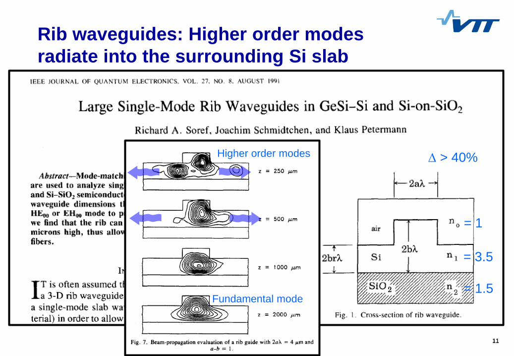
Rib waveguides: Higher order modes
radiate into the surrounding Si slab
= 1
= 3.5
= 1.5
> 40%Higher order modes
Fundamental mode

1212
Basics of strip waveguides
Highly multi-moded (MM) waveguides
Can be used in SM waveguide circuits IF light is
kept in the fundamental mode
Adiabatic rib-strip converters are a key
component
Benefits:
Small propagation loss (0.1-0.15 dB/cm)
Zero birefringence possible
Euler bends reaching down to 1 µm bending radius
No cross-talk between waveguides (dense arrays)
Limitations:
Risk of exciting higher-order modes and causing
modal interference
1313
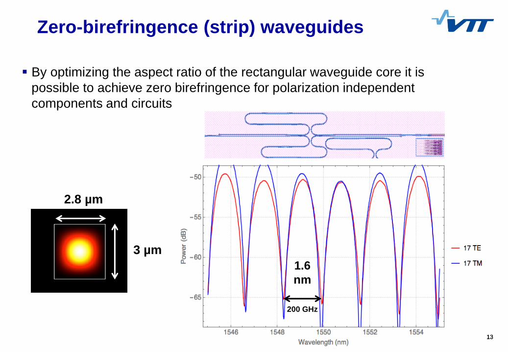
Zero-birefringence (strip) waveguides
2.8 µm
1.6
nm
200 GHz
By optimizing the aspect ratio of the rectangular waveguide core it is
possible to achieve zero birefringence for polarization independent
components and circuits
3 µm

1414
Tolerance to high optical power
Waveguide core
height x width:
Waveguide core
area
Estimated maximum
optical power
0.22 x 0.45 µ m (nanowire) 0.2 µ m2 0.02 W
3 x 1 µ m (narrow strip) 3 µ m2 0.3 W
3 x 3 µ m (strip/rib) 9 µ m2 0.9 W
3 x 10 µ m (wide strip/rib) 30 µ m2 3 W
12 x 10µ m (strip/rib) 120 µ m2 12 W
12 x 20 µ m (wide strip/rib) 240 µ m2 24 W
Nonlinear effects depend on intensity, which depends on optical power
and the cross-section area of the waveguide mode
Larger waveguides tolerate higher optical powers

15
Shrinking the bend size
16
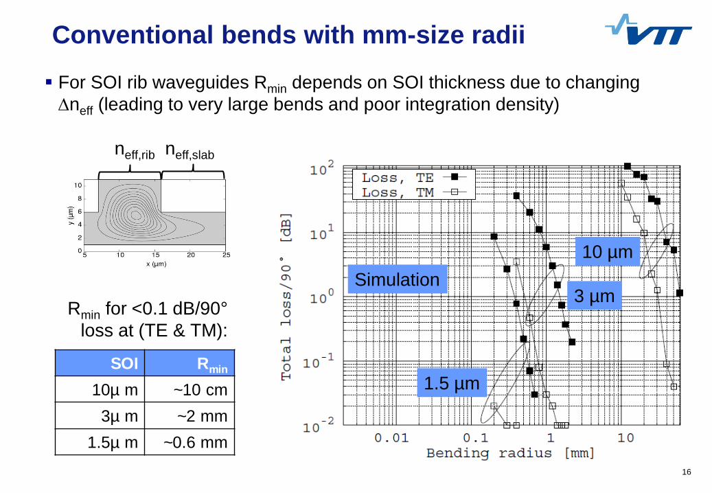
Rmin for <0.1 dB/90°
loss at (TE & TM):
1.5 µm
3 µm
10 µm
SOI Rmin
10 µ m ~10 cm
3 µ m ~2 mm
1.5 µ m ~0.6 mm
For SOI rib waveguides Rmin depends on SOI thickness due to changing
neff (leading to very large bends and poor integration density)
neff,rib neff,slab
Simulation
Conventional bends with mm-size radii
1717
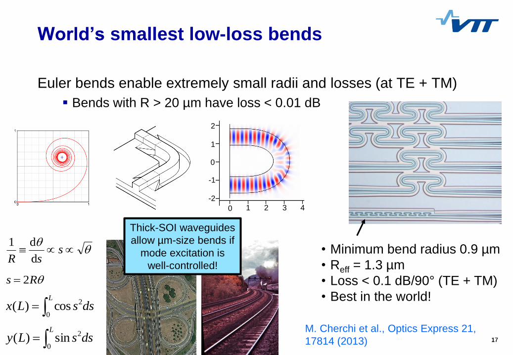
World’s smallest low-loss bends
Euler bends enable extremely small radii and losses (at TE + TM)
Bends with R > 20 µm have loss < 0.01 dB
0
1
2
-1
-2
0 1 2 3 4
• Minimum bend radius 0.9 µm
• Reff = 1.3 µm
• Loss < 0.1 dB/90° (TE + TM)
• Best in the world!
ssR d
d1
Rs 2
L
dssLy0
2sin)(
L
dssLx0
2cos)(
M. Cherchi et al., Optics Express 21,
17814 (2013)
Thick-SOI waveguides
allow µm-size bends if
mode excitation is
well-controlled!
1818
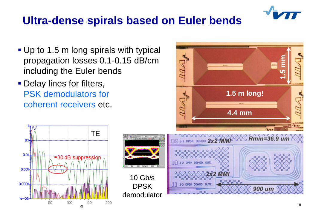
Ultra-dense spirals based on Euler bends
Up to 1.5 m long spirals with typical
propagation losses 0.1-0.15 dB/cm
including the Euler bends
Delay lines for filters,
PSK demodulators for
coherent receivers etc.4.4 mm
1.5
mm
1.5 m long!
10 Gb/s
DPSK
demodulator

2020
Reduced TIR mirror losses with wider
waveguides and curved mirror facets
State-of-the-art of total internal reflection mirrors:
0.3 dB/90°
Experimental results from TIR mirrors with
curved facets in strip waveguides:
0.075 dB/90° at TE
0.104 dB/90° for TE+TM
PW'15: T. Aalto et al.,
Proc. SPIE 9367-9Simulations
0.02 dB
0.02 dB

21
The 3 µm SOI platform
2222
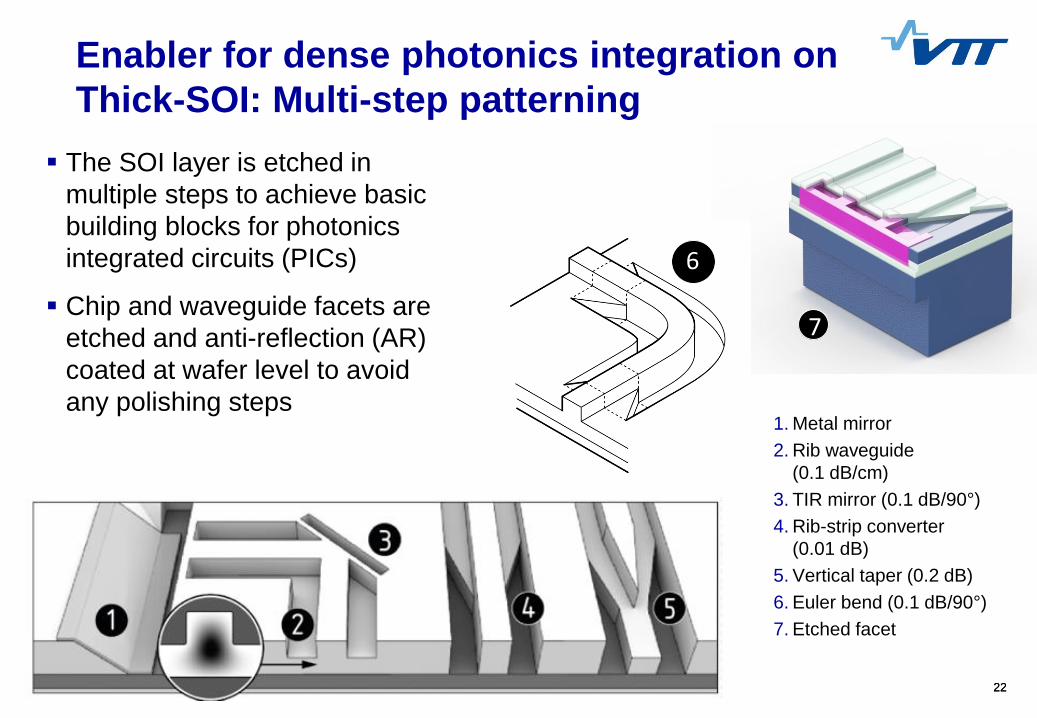
Enabler for dense photonics integration on
Thick-SOI: Multi-step patterning
1. Metal mirror
2. Rib waveguide
(0.1 dB/cm)
3. TIR mirror (0.1 dB/90°)
4. Rib-strip converter
(0.01 dB)
5. Vertical taper (0.2 dB)
6. Euler bend (0.1 dB/90°)
7. Etched facet
6
The SOI layer is etched in
multiple steps to achieve basic
building blocks for photonics
integrated circuits (PICs)
Chip and waveguide facets are
etched and anti-reflection (AR)
coated at wafer level to avoid
any polishing steps
7

2323
3 µm SOI platform (available as MPW)
Example components:
Compact AWG and Echelle multiplexers
Short MMI couplers for advanced filters
and AMZI-multiplexers
DPSK demodulator for 10 Gb/s based
on a low-loss delay line (~0.1 dB/cm)
Dense strip waveguide arrays
Ultra-compact and low-loss spirals

25
typical losses: 0.15 dB
100 nm BW@1dB
typical imbalance: < 0.2 dB
extinction ratio in MZIs: 27 dB
2 x 2
typical losses: 0.15 dB
100 nm BW@1dB
typical imbalance: < 0.01 dB
STRIP waveguide (full etch)
Multi-mode interference couplers (MMIs)
1 x 2

26
0 10 20 30 40 50 60 70 80 90 100 110 120 130 140 150 160 170 180 190 200 210 220 230 240 250 260 270 z/um
-3.5-3.0
-2.5-2.0
-1.5-1.0
-0.50.0
0.51.0
1.52.0
2.53.0
x/um
100 68.4
29.0
L = 35.5 μm
Δw = 500 nm
g g50/50 50/50
w+Δw
w-Δw
IN1
IN2
OUT1
OUT2
a
b
c
0 10 20 30 40 50 60 70 80 90 100 110 120 130 140 150 160 170 180 190 200 210 220 230 240 250 260 270 z/um
-3.5-3.0
-2.5-2.0
-1.5-1.0
-0.50.0
0.51.0
1.52.0
2.53.0
x/um
100
29.0
69.4
25 30 35 40 45 50-20
-15
-10
-5
0
L (m)
Tra
nsm
issio
n (
dB
)
T22
T21
25 30 35 40 45 50-20
-15
-10
-5
0
L (m)
Tra
nsm
issio
n (
dB
)
T11
T12
a b
c
25 30 35 40 45 50
0
5
10
15
20
L (m)
Po
we
r im
bala
nce b
ar-
cro
ss
(dB
)
port 1
port 2
25 30 35 40 45 500
20
40
60
80
100
L (m)
No
rmaliz
ed
pow
er
pe
rcen
tag
e
T12
T21
T11
T22
a b
-200 -150 -100 -50 035
40
45
50
55
60
width change (nm)
L (m
)
Sensitivity to width changes
"Unconstrained splitting ratios in compact double-MMI couplers,"
Opt. Express 22, 9245–9253 (2014).
Asymmetric Mach-Zehnder Interferometers

29
Compact AWGs for any channel spacing
10 mm 5 mm
30
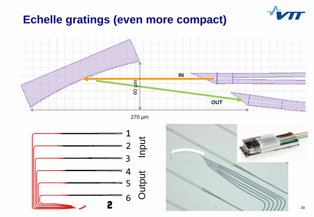
270 µm
60
µm
IN
OUT
1
2
3
45
6
Inp
ut
Ou
tpu
t
Echelle gratings (even more compact)
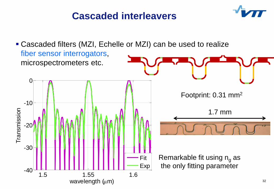
32
Remarkable fit using ng as
the only fitting parameter
1.5 1.55 1.6-40
-30
-20
-10
0
wavelength (m)
Tra
nsm
issio
n
Fit
Exp
Cascaded interleavers
1.7 mm
Footprint: 0.31 mm2
Cascaded filters (MZI, Echelle or MZI) can be used to realize
fiber sensor interrogators,
microspectrometers etc.
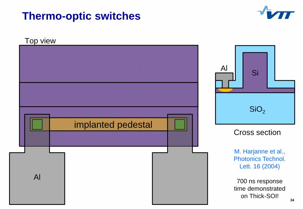
3434
implanted pedestal
Al
Cross section
AlSi
SiO2
Top view
Thermo-optic switches
M. Harjanne et al.,
Photonics Technol.
Lett. 16 (2004)
700 ns response
time demonstrated
on Thick-SOI!

3636
Electro-optic switches
Top view
Cross section
Al Si
SiO2
Al
n
Al
pp n
Targeting 10 MHz
(work in progress)
3838
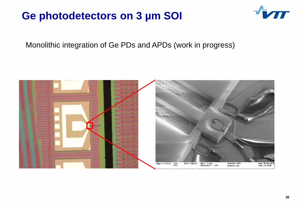
Ge photodetectors on 3 µm SOI
Monolithic integration of Ge PDs and APDs (work in progress)

40
To combine the best properties of different materials (Si, III-V)
To avoid unnecessary compromises in performance
To simplify wafer processing
To reduce development time
To increase manufacturing volumes
...or because monolithic solutions are not (yet) available
Monolithic devices
on submicron SOI
Why hybrid integration?

41
Automated flip-chip bonding with sub-micron accuracy
Passive mechanical alignment vertically (±0.1 µm)
Machine vision for horizontal alignment
Excellent heat dissipation
through thin Au pads
No solder bumps
Heat Heat
T. Aalto et al., Proc. SPIE
7941-28 (PW'11)
M. Kapulainen et al.,
Proc. GFP 2014
Au-Au thermo compression bonding
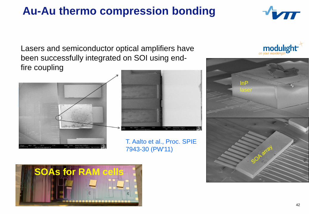
42
T. Aalto et al., Proc. SPIE
7943-30 (PW'11)
Lasers and semiconductor optical amplifiers have
been successfully integrated on SOI using end-
fire coupling
InP
laser
Au-Au thermo compression bonding
SOAs for RAM cells

44
The 12 µm SOI platform
4545
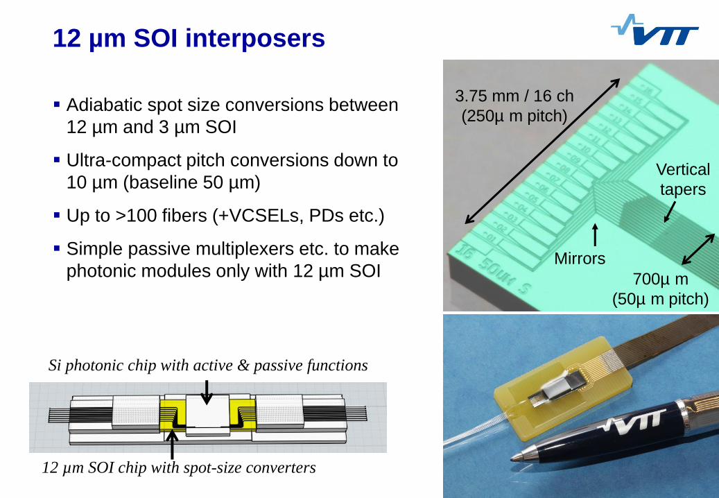
12 µm SOI interposers
Si photonic chip with active & passive functions
12 µm SOI chip with spot-size converters
Adiabatic spot size conversions between
12 µm and 3 µm SOI
Ultra-compact pitch conversions down to
10 µm (baseline 50 µm)
Up to >100 fibers (+VCSELs, PDs etc.)
Simple passive multiplexers etc. to make
photonic modules only with 12 µm SOI
3.75 mm / 16 ch
(250 µ m pitch)
700 µ m
(50 µ m pitch)
Vertical
tapers
Mirrors

4747
12 µm SOI interposers for packaging
220 nm SOI chips
12 µm SOI interposers to package 220 nm SOI chips:
• Inverse tapers or other spot-size converters
are needed

4848
12 µm SOI platform
Mockup demo for integrating VCSELs and PDs on 12 µm SOI
(without any 220 nm or 3 µm SOI chips)
Suitable for low-cost and compact
datacom transceivers
SMF array
in V-grooves
12 µm SOI chip
(5x10 mm)
with MUX
VCSELs with 25 Gbps
direct modulation
Photodiodes
up to 40 Gbps
Driver and TIA
(dummies)
Passive electronics
25 Gbit/s VCSEL

5050
12 µm SOI platform
51
Design support and
access in Thick-SOI
5252
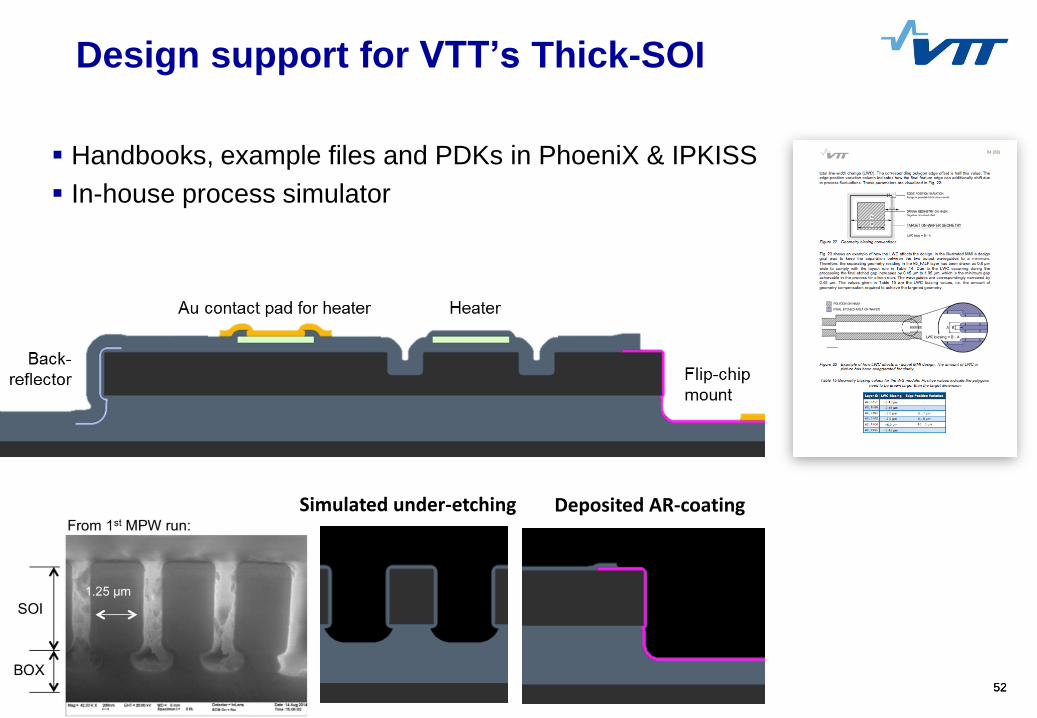
Design support for VTT’s Thick-SOI
Handbooks, example files and PDKs in PhoeniX & IPKISS
In-house process simulator
Simulated under-etching Deposited AR-coating
5353
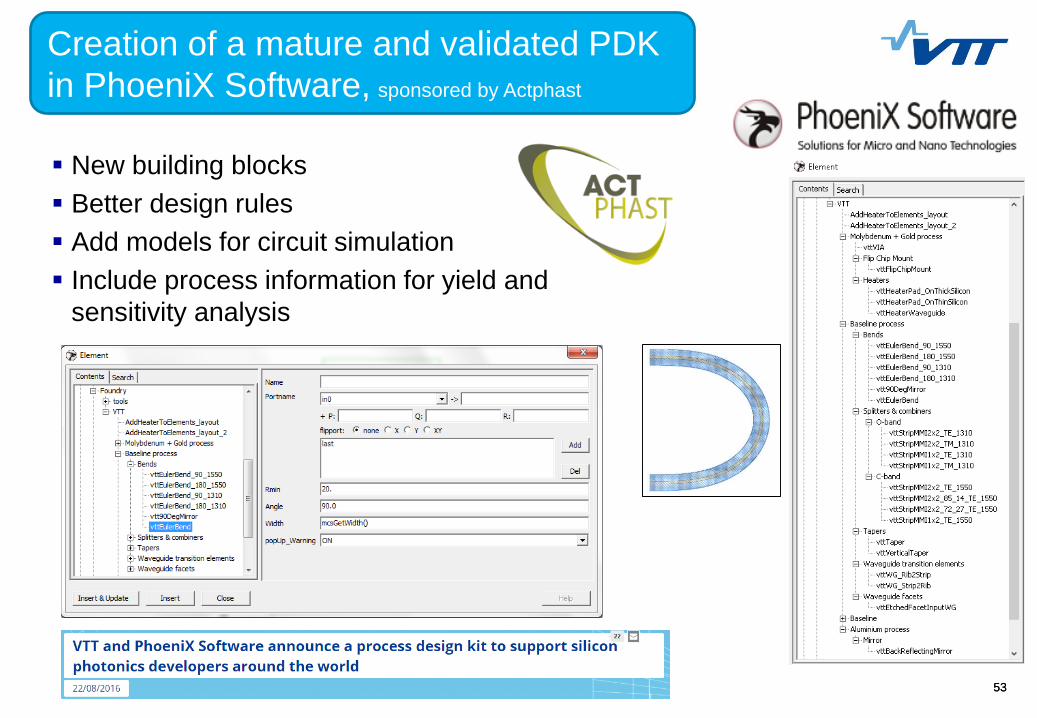
VTT’s silicon photonics platform
New building blocks
Better design rules
Add models for circuit simulation
Include process information for yield and
sensitivity analysis
Creation of a mature and validated PDK
in PhoeniX Software, sponsored by Actphast
5454
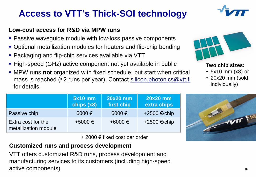
Access to VTT’s Thick-SOI technology
Low-cost access for R&D via MPW runs
Passive waveguide module with low-loss passive components
Optional metallization modules for heaters and flip-chip bonding
Packaging and flip-chip services available via VTT
High-speed (GHz) active component not yet available in public
MPW runs not organized with fixed schedule, but start when critical
mass is reached (≈2 runs per year). Contact [email protected]
for details.
Customized runs and process development
VTT offers customized R&D runs, process development and
manufacturing services to its customers (including high-speed
active components)
Two chip sizes:
• 5x10 mm (x8) or
• 20x20 mm (sold
individually)
5x10 mm
chips (x8)
20x20 mm
first chip
20x20 mm
extra chips
Passive chip 6000 € 6000 € +2500 €/chip
Extra cost for the
metallization module
+5000 € +6000 € +2500 €/chip
+ 2000 € fixed cost per order

55
Application examples

5656
Application example on 3 µm SOI
Medical imaging device based on
Optical Coherence Tomography (OCT):
Similar to ultrasound imaging, but with light
Light reflected back from a tissue is
combined with a reference signal from the
same low-coherence light source (SLED)
Strong interference observed when the
reference and signal arms have same length
Imaging cross-sections inside the tissue
Scanning the beam enables 3D imaging
Concept proved and first OCT imagers built
based on VTT’s 3 µ m SOI platform

5757
DPSK demodulation with delay lines
AMZIs can convert phase modulation to amplitude modulation
Delay 8.8 mm
(in 0.4 mm2)
OFC’15: Vyrsokinos et al.,
"DPSK-Demodulation
based on Ultra-Compact
micron-scale SOI
platform”
GFP’14: M. Cherchi et al.

58
Conclusions

5959
VTT’s silicon photonics platform
Main benefits of the Thick-SOI approach at VTT:
Customized and MPW runs
Scalability to low-cost mass production via VTT up to
millions of chips
High integration density (small dies and modules)
Small optical losses (~0.1 dB/cm)
Small polarization dependency (zero birefringence is possible)
Tolerance to high optical powers (scales with core area)
Single-mode operation (almost independent of wavelength)
Ultra-wide bandwidth within 1.2–6 µ m wavelength range
Efficient thermal management
5x10 mm
Si chip

TECHNOLOGY FOR BUSINESS