VS-VSK.136/142/162..PbF Series - Vishay Intertechnology · VS-VSK.136..PbF, VS-VSK.142..PbF,...
14
VS-VSK.136..PbF, VS-VSK.142..PbF, VS-VSK.162..PbF Series www.vishay.com Vishay Semiconductors Revision: 27-Jul-2018 1 Document Number: 94513 For technical questions within your region: [email protected] , [email protected] , [email protected] THIS DOCUMENT IS SUBJECT TO CHANGE WITHOUT NOTICE. THE PRODUCTS DESCRIBED HEREIN AND THIS DOCUMENT ARE SUBJECT TO SPECIFIC DISCLAIMERS, SET FORTH AT www.vishay.com/doc?91000 Thyristor/Diode and Thyristor/Thyristor, 135 A to 160 A (INT-A-PAK Power Modules) FEATURES • High voltage • Electrically isolated by DBC ceramic (AI 2 O 3 ) • 3500 V RMS isolating voltage • Industrial standard package • High surge capability • Glass passivated chips • Modules uses high voltage power thyristor/diodes in three basic configurations • Simple mounting • UL approved file E78996 • Designed and qualified for multiple level • Material categorization: for definitions of compliance please see www.vishay.com/doc?99912 APPLICATIONS • DC motor control and drives • Battery charges • Welders • Power converters • Lighting control • Heat and temperature control ELECTRICAL SPECIFICATIONS PRIMARY CHARACTERISTICS I T(AV) 135 A to 160 A Type Modules - thyristor, standard Package INT-A-PAK INT-A-PAK MAJOR RATINGS AND CHARACTERISTICS SYMBOL CHARACTERISTICS VSK.136.. VSK.142.. VSK.162.. UNITS I T(AV) 85 °C 135 140 160 A I T(RMS) 300 310 355 A I TSM 50 Hz 3200 4500 4870 60 Hz 3360 4712 5100 I 2 t 50 Hz 51.5 102 119 kA 2 s 60 Hz 47 92.5 108 I 2 t 515.5 1013 1190 kA 2 s V RRM Range 400 to 1600 400 to 1600 400 to 1600 V T J Range -40 to +125 °C VOLTAGE RATINGS TYPE NUMBER VOLTAGE CODE V RRM /V DRM , MAXIMUM REPETITIVE PEAK REVERSE VOLTAGE V V RSM /V DSM , MAXIMUM NON-REPETITIVE PEAK REVERSE VOLTAGE V I RRM /I DRM AT 125 °C mA VS-VSK.136 VS-VSK.142 VS-VSK.162 04 400 500 50 08 800 900 12 1200 1300 14 1400 1500 16 1600 1700
Transcript of VS-VSK.136/142/162..PbF Series - Vishay Intertechnology · VS-VSK.136..PbF, VS-VSK.142..PbF,...
VS-VSK.136..PbF, VS-VSK.142..PbF, VS-VSK.162..PbF Serieswww.vishay.com Vishay Semiconductors
Revision: 27-Jul-2018 1 Document Number: 94513For technical questions within your region: [email protected], [email protected], [email protected]
THIS DOCUMENT IS SUBJECT TO CHANGE WITHOUT NOTICE. THE PRODUCTS DESCRIBED HEREIN AND THIS DOCUMENTARE SUBJECT TO SPECIFIC DISCLAIMERS, SET FORTH AT www.vishay.com/doc?91000
Thyristor/Diode and Thyristor/Thyristor, 135 A to 160 A (INT-A-PAK Power Modules)
FEATURES• High voltage
• Electrically isolated by DBC ceramic (AI2O3)
• 3500 VRMS isolating voltage
• Industrial standard package
• High surge capability
• Glass passivated chips
• Modules uses high voltage power thyristor/diodes in three basic configurations
• Simple mounting
• UL approved file E78996
• Designed and qualified for multiple level
• Material categorization: for definitions of compliance please see www.vishay.com/doc?99912
APPLICATIONS• DC motor control and drives
• Battery charges
• Welders
• Power converters
• Lighting control
• Heat and temperature control
ELECTRICAL SPECIFICATIONS
PRIMARY CHARACTERISTICSIT(AV) 135 A to 160 A
Type Modules - thyristor, standard
Package INT-A-PAK
INT-A-PAK
MAJOR RATINGS AND CHARACTERISTICSSYMBOL CHARACTERISTICS VSK.136.. VSK.142.. VSK.162.. UNITS
IT(AV) 85 °C 135 140 160 A
IT(RMS) 300 310 355
AITSM
50 Hz 3200 4500 4870
60 Hz 3360 4712 5100
I2t50 Hz 51.5 102 119
kA2s60 Hz 47 92.5 108
I2t 515.5 1013 1190 kA2s
VRRM Range 400 to 1600 400 to 1600 400 to 1600 V
TJ Range -40 to +125 °C
VOLTAGE RATINGS
TYPENUMBER
VOLTAGE CODE
VRRM/VDRM, MAXIMUM REPETITIVE PEAK REVERSE VOLTAGE
V
VRSM/VDSM, MAXIMUM NON-REPETITIVE PEAK REVERSE VOLTAGE
V
IRRM/IDRMAT 125 °C
mA
VS-VSK.136VS-VSK.142VS-VSK.162
04 400 500
50
08 800 900
12 1200 1300
14 1400 1500
16 1600 1700
VS-VSK.136..PbF, VS-VSK.142..PbF, VS-VSK.162..PbF Serieswww.vishay.com Vishay Semiconductors
Revision: 27-Jul-2018 2 Document Number: 94513For technical questions within your region: [email protected], [email protected], [email protected]
THIS DOCUMENT IS SUBJECT TO CHANGE WITHOUT NOTICE. THE PRODUCTS DESCRIBED HEREIN AND THIS DOCUMENTARE SUBJECT TO SPECIFIC DISCLAIMERS, SET FORTH AT www.vishay.com/doc?91000
ON-STATE CONDUCTIONPARAMETER SYMBOL TEST CONDITIONS VSK.136 VSK.142 VSK.162 UNITS
Maximum average on-state current at case temperature IT(AV) 180° conduction, half sine wave
135 140 160 A
85 85 85 °C
Maximum RMS on-state current IT(RMS) As AC switch 300 310 355
AMaximum peak, one-cycle on-state, non-repetitive surge current
ITSM
t = 10 ms No voltagereapplied
Sine half wave,initial TJ = TJ maximum
3200 4500 4870
t = 8.3 ms 3360 4712 5100
t = 10 ms 100 % VRRM reapplied
2700 3785 4100
t = 8.3 ms 2800 3963 4300
Maximum I2t for fusing I2t
t = 10 ms No voltagereapplied
51.5 102 119
kA2st = 8.3 ms 47 92.5 108
t = 10 ms 100 % VRRM reapplied
36.5 71.6 84
t = 8.3 ms 33.3 65.4 76.7
Maximum I2t for fusing I2t t = 0.1 ms to 10 ms, no voltage reapplied 515.5 1013 1190 kA2s
Low level value of threshold voltage VT(TO)1 (16.7 % x x IT(AV) < I < x IT(AV)), TJ maximum 0.86 0.83 0.8V
High level value of threshold voltage VT(TO)2 (I > x IT(AV)), TJ maximum 1.05 1 0.98
Low level value on-stateslope resistance rt1 (16.7 % x x IT(AV) < I < x IT(AV)), TJ maximum 2.02 1.78 1.67
mHigh level value on-stateslope resistance rt2 (I > x IT(AV)), TJ maximum 1.65 1.43 1.38
Maximum on-state voltage drop VTM ITM = x IT(AV), TJ = 25 °C, 180° conduction 1.57 1.55 1.54 V
Maximum forward voltage drop VFM ITM = x IT(AV), TJ = 25 °C, 180° conduction 1.57 1.55 1.54 V
Maximum holding current IH Anode supply = 6 V initial IT = 30 A, TJ = 25 °C 200mA
Maximum latching current ILAnode supply = 6 V resistive load = 1 Gate pulse: 10 V, 100 μs, TJ = 25 °C 400
SWITCHINGPARAMETER SYMBOL TEST CONDITIONS VALUES UNITS
Typical delay time tgdTJ = 25 °C Gate current = 1 A, dlg/dt = 1 A/μs
Vd = 0.67 % VDRM
1
μsTypical rise time tgr 2
Typical turn-off time tqITM = 300 A, - dl/dt = 15 A/μs; TJ = TJ maximumVR = 50 V; dV/dt = 20 V/μs; gate 0 V, 100 50 to 200
BLOCKINGPARAMETER SYMBOL TEST CONDITIONS VALUES UNITS
Maximum peak reverse andoff-state leakage current
IRRM,IDRM
TJ = 125 °C 50 mA
RMS insulation voltage VINS50 Hz, circuit to base,all terminals shorted, t = 1 s 3500 V
Critical rate of rise ofoff-state voltage dV/dt TJ = TJ maximum,
exponential to 67 % rated VDRM1000 V/μs
VS-VSK.136..PbF, VS-VSK.142..PbF, VS-VSK.162..PbF Serieswww.vishay.com Vishay Semiconductors
Revision: 27-Jul-2018 3 Document Number: 94513For technical questions within your region: [email protected], [email protected], [email protected]
THIS DOCUMENT IS SUBJECT TO CHANGE WITHOUT NOTICE. THE PRODUCTS DESCRIBED HEREIN AND THIS DOCUMENTARE SUBJECT TO SPECIFIC DISCLAIMERS, SET FORTH AT www.vishay.com/doc?91000
Note• Table shows the increment of thermal resistance RthJC when devices operate at different conduction angles than DC
TRIGGERINGPARAMETER SYMBOL TEST CONDITIONS VALUES UNITS
Maximum peak gate power PGM tp 5 ms, TJ = TJ maximum 12W
Maximum average gate power PG(AV) f = 50 Hz, TJ = TJ maximum 3
Maximum peak gate current IGM
tp 5 ms, TJ = TJ maximum3 A
Maximum peak negativegate voltage
- VGT 10
VMaximum required DCgate voltage to trigger
VGT
TJ = - 40 °C
Anode supply = 6 V, resistive load; Ra = 1
4
TJ = 25 °C 2.5
TJ = TJ maximum 1.7
Maximum required DC gate current to trigger
IGT
TJ = - 40 °C 270
mATJ = 25 °C 150
TJ = TJ maximum 80
Maximum gate voltage that will not trigger
VGD
TJ = TJ maximum, rated VDRM applied0.3 V
Maximum gate current that will not trigger
IGD 10 mA
Maximum rate of rise of turned-on current
dI/dt TJ = TJ maximum, ITM = 400 A rated VDRM applied 300 A/μs
THERMAL AND MECHANICAL SPECIFICATIONSPARAMETER SYMBOL TEST CONDITIONS VSK.136 VSK.142 VSK.162 UNITS
Maximum junction operatingtemperature range
TJ -40 to +125
°CMaximum storage temperature range
TStg -40 to +150
Maximum thermal resistance,junction to case per junction
RthJC DC operation 0.18 0.18 0.16
K/WMaximum thermal resistance,case to heatsink per module
RthCS Mounting surface, smooth, flat and greased 0.05
Mountingtorque ± 10 %
IAP to heatsink A mounting compound is recommended and the torque should be rechecked after a period of3 hours to allow for the spread of the compound. Lubricated threads.
4 to 6 Nmbusbar to IAP
Approximate weight200 g
7.1 oz.
Case style INT-A-PAK
R CONDUCTION PER JUNCTION
DEVICESSINUSOIDAL CONDUCTION
AT TJ MAXIMUMRECTANGULAR CONDUCTION
AT TJ MAXIMUM UNITS180° 120° 90° 60° 30° 180° 120° 90° 60° 30°
VSK.136 0.007 0.01 0.013 0.0155 0.017 0.009 0.012 0.014 0.015 0.017
K/WVSK.142 0.0019 0.0019 0.0020 0.0020 0.0021 0.0018 0.0022 0.0023 0.0023 0.0020
VSK.162 0.0030 0.0031 0.0032 0.0033 0.0034 0.0029 0.0036 0.0039 0.0041 0.0040
VS-VSK.136..PbF, VS-VSK.142..PbF, VS-VSK.162..PbF Serieswww.vishay.com Vishay Semiconductors
Revision: 27-Jul-2018 4 Document Number: 94513For technical questions within your region: [email protected], [email protected], [email protected]
THIS DOCUMENT IS SUBJECT TO CHANGE WITHOUT NOTICE. THE PRODUCTS DESCRIBED HEREIN AND THIS DOCUMENTARE SUBJECT TO SPECIFIC DISCLAIMERS, SET FORTH AT www.vishay.com/doc?91000
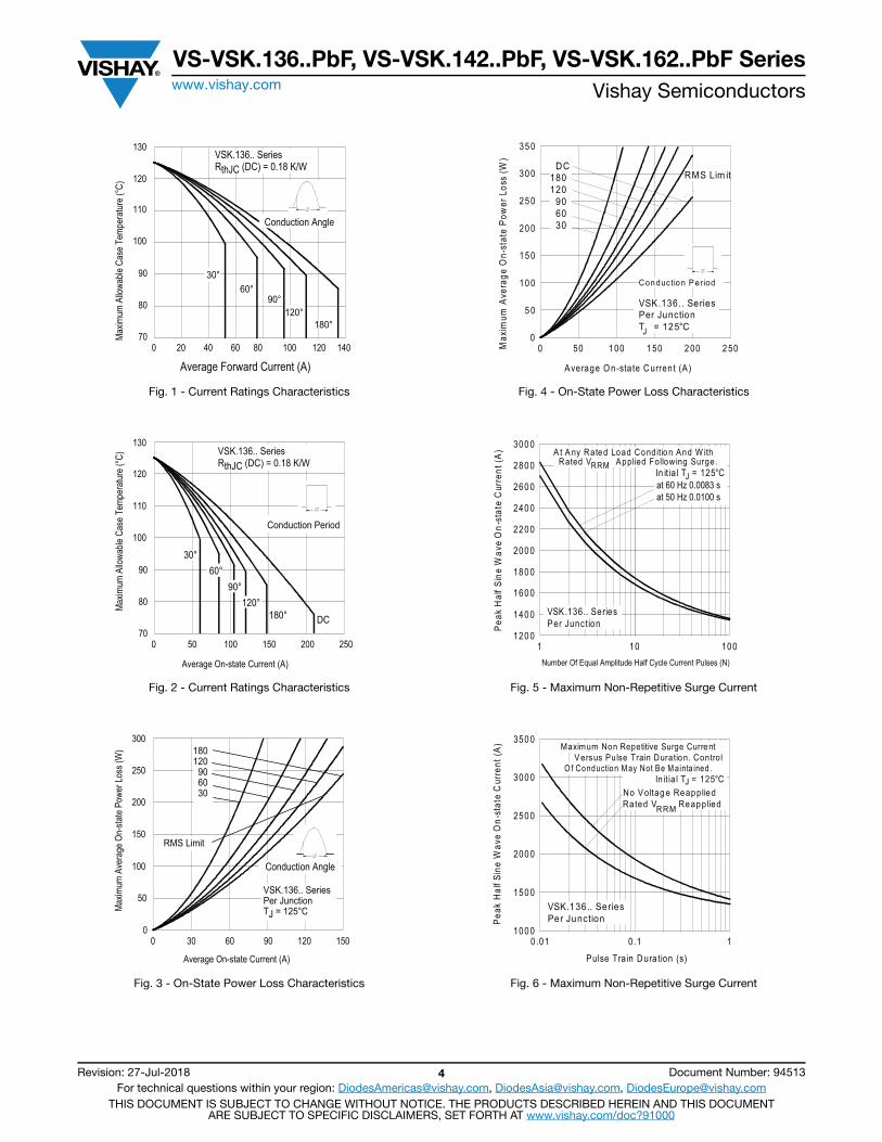
Fig. 1 - Current Ratings Characteristics
Fig. 2 - Current Ratings Characteristics
Fig. 3 - On-State Power Loss Characteristics
Fig. 4 - On-State Power Loss Characteristics
Fig. 5 - Maximum Non-Repetitive Surge Current
Fig. 6 - Maximum Non-Repetitive Surge Current
70
80
90
100
110
120
130
0 20 40 60 80 100 120 140
30°60°
90°120°
180°
Max
imum
Allo
wable
Cas
e Te
mpe
ratu
re (°
C)
Conduction Angle
Average Forward Current (A)
VSK.136.. SeriesRthJC (DC) = 0.18 K/W
70
80
90
100
110
120
130
0 50 100 150 200 250
DC
30°60°
90°120°
180°
Average On-state Current (A)
Max
imum
Allo
wable
Cas
e Te
mpe
ratu
re (°
C)
Conduction Period
VSK.136.. SeriesRthJC (DC) = 0.18 K/W
0
50
100
150
200
250
300
0 30 60 90 120 150
RMS Limit
Conduction Angle
Max
imum
Ave
rage
On-
state
Pow
er L
oss (
W)
Average On-state Current (A)
180120 90 60 30
VSK.136.. SeriesPer JunctionTJ = 125°C
0
5 0
10 0
15 0
20 0
25 0
30 0
35 0
0 50 1 00 1 50 2 00 2 50
RMS Lim it
Conduc tio n P er iod
Max
imum
Ave
rage
On-
stat
e Po
wer
Los
s (W
)
A verage O n-sta te C urrent (A)
DC180120
906030
VSK.136.. SeriesPer JunctionT = 125°CJ
120 0
140 0
160 0
180 0
200 0
220 0
240 0
260 0
280 0
300 0
001011Number Of Equal Amplitude Half Cycle Current Pulses (N)
A t A ny Rate d Load Co nditio n And W ithRated V Applied Follow ing Surge .RRM
Peak
Hal
f Sin
e W
ave
On-
stat
e C
urre
nt (A
)
In it ia l T = 125°Cat 60 Hz 0.0083 sat 50 Hz 0.0100 s
J
VSK.136.. SeriesPer Junction
100 0
150 0
200 0
250 0
300 0
350 0
11.010.0
Peak
Hal
f Sin
e W
ave
On-
stat
e C
urre
nt (A
)
Pulse Tra in D ura tion (s)
Maximum Non Repetitive Surge Current
O f Conduction M ay Not Be M ainta ined .
VSK.136.. SeriesPer Junction
In it ia l T = 125°CNo Voltag e ReappliedRated V Reapplied
J
RRM
V ersus Pulse Train Duratio n. Control
VS-VSK.136..PbF, VS-VSK.142..PbF, VS-VSK.162..PbF Serieswww.vishay.com Vishay Semiconductors
Revision: 27-Jul-2018 5 Document Number: 94513For technical questions within your region: [email protected], [email protected], [email protected]
THIS DOCUMENT IS SUBJECT TO CHANGE WITHOUT NOTICE. THE PRODUCTS DESCRIBED HEREIN AND THIS DOCUMENTARE SUBJECT TO SPECIFIC DISCLAIMERS, SET FORTH AT www.vishay.com/doc?91000
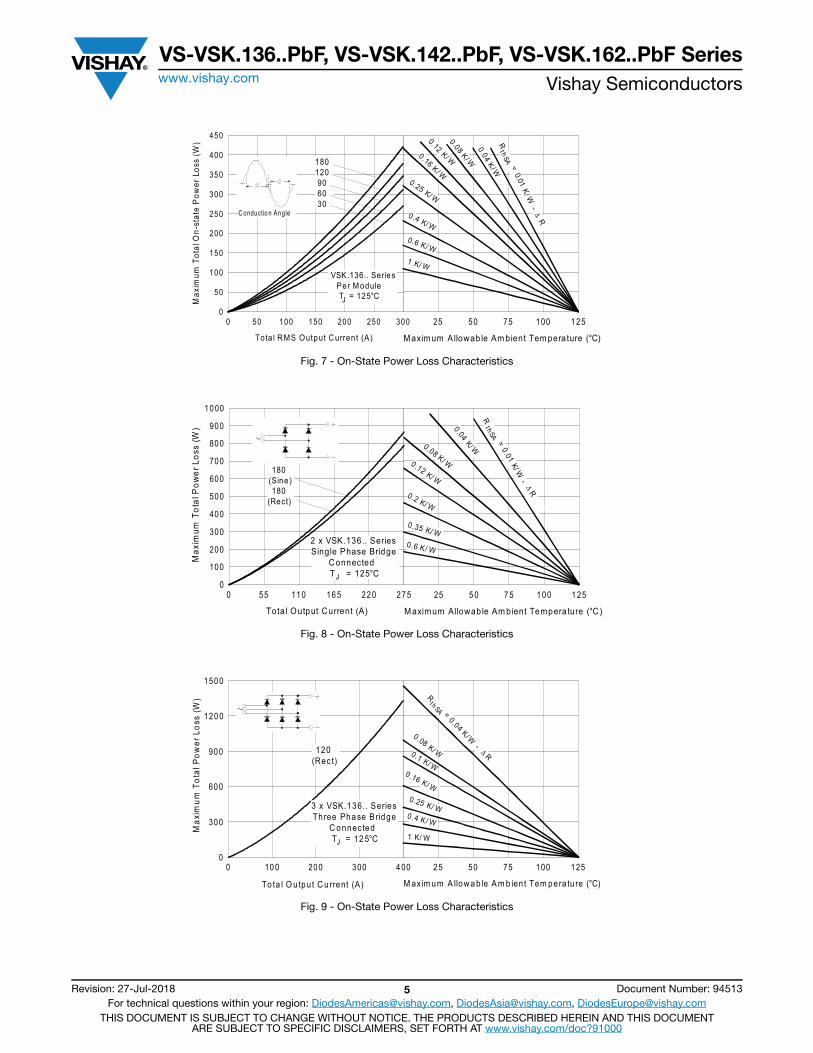
Fig. 7 - On-State Power Loss Characteristics
Fig. 8 - On-State Power Loss Characteristics
Fig. 9 - On-State Power Loss Characteristics
0 25 50 75 100 1 25
M axim um A llowab le Am bient Tem pera ture (°C)0.04
K /WR
=0.01
K/ W- Δ
R
t hSA
0 .08 K/ W
0.12 K/ W0 .16 K/ W
0.4 K/ W
0.25 K/ W
0.6 K/ W
1 K/ W
0
50
100
150
200
250
300
350
400
450
0 50 100 150 200 250 300
180120906030
Tota l RMS Output C urrent (A)
Max
imum
Tot
al O
n-st
ate
Pow
er L
oss
(W)
C onductio n Angle
VSK.136.. SeriesPer M oduleT = 125°CJ
0 25 5 0 7 5 1 00 1 25
M axim um Allowab le Am bient Tempera ture (°C)
0.04K/ W0.08 K/ W0.12 K/ W
0.2 K/ W
0.35 K/ W0.6 K/ W
0
100
200
300
400
500
600
700
800
900
10 00
0 55 110 16 5 22 0 27 5
Total Output Current (A)
Max
imum
Tot
al P
ower
Los
s (W
)
2 x VSK.136.. SeriesSingle Phase Bridge
ConnectedT = 125°CJ
180(Sine)180
(Rect)
R
=0.01
K/ W-
Δ R
t hAS
0 25 50 75 100 125
M axim um A llo w a b le A m b ien t Tem pera tu re (°C)
R
=0.04 K/ W
-Δ R
0 .08 K/ W0.1 K/ W0.16 K/ W
0.25 K/ W0.4 K/ W
1 K/ W
thSA
0
300
600
900
120 0
150 0
0 10 0 200 300 4 00
To ta l O u tpu t C urrent (A)
Max
imum
Tot
al P
ower
Los
s (W
)
120(Rec t)
3 x VSK.136.. SeriesThree Pha se B ridge
C o nnec tedT = 12 5°CJ
VS-VSK.136..PbF, VS-VSK.142..PbF, VS-VSK.162..PbF Serieswww.vishay.com Vishay Semiconductors
Revision: 27-Jul-2018 6 Document Number: 94513For technical questions within your region: [email protected], [email protected], [email protected]
THIS DOCUMENT IS SUBJECT TO CHANGE WITHOUT NOTICE. THE PRODUCTS DESCRIBED HEREIN AND THIS DOCUMENTARE SUBJECT TO SPECIFIC DISCLAIMERS, SET FORTH AT www.vishay.com/doc?91000
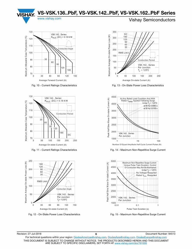
Fig. 10 - Current Ratings Characteristics
Fig. 11 - Current Ratings Characteristics
Fig. 12 - On-State Power Loss Characteristics
Fig. 13 - On-State Power Loss Characteristics
Fig. 14 - Maximum Non-Repetitive Surge Current
Fig. 15 - Maximum Non-Repetitive Surge Current
70
80
90
10 0
11 0
12 0
13 0
0 30 60 9 0 1 20 150
3060
90120
180
Max
imum
Allo
wab
le C
ase
Tem
pera
ture
(°C)
C onduction Angle
Average Forwa rd C urrent (A)
VSK.142.. SeriesR (D C ) = 0.18 K/WthJC
70
80
90
1 00
1 10
1 20
1 30
0 50 10 0 150 20 0 25 0
DC
3060
90120
180
Average O n-state C urrent (A)
Max
imum
Allo
wab
le C
ase
Tem
pera
ture
(°C)
C o n duc tio n P er iod
VSK.142.. Se riesR (D C ) = 0 .18 K /WthJC
0
50
10 0
15 0
20 0
25 0
0 30 60 90 120 150
RMS Lim it
C ond uc tion Angle
Max
imum
Ave
rage
On-
stat
e Po
wer
Los
s (W
)
Average O n-state C urren t (A )
180120
906030
VSK.142.. Series Per JunctionT = 125°CJ
0
50
10 0
15 0
20 0
25 0
30 0
35 0
0 50 100 150 200 250
DC180120
906030
RM S L im it
C o ndu c tio n Pe r io d
Max
imum
Ave
rage
On-
stat
e Po
wer
Los
s (W
)
Average O n-state C urren t (A )
VSK .142.. Se riesPer Junc tio nT = 12 5°CJ
150 0
200 0
250 0
300 0
350 0
400 0
450 0
001011Num b er O f Equa l Am p litud e H a lf Cy cle C urrent Pulses (N)
Peak
Hal
f Sin
e W
ave
On-
stat
e C
urre
nt (A
)
JIn itia l T = 125°Cat 60 Hz 0.0083 sat 50 Hz 0.0100 s
A t A ny Rated Load Co nditio n And W ithRated V App lied Follow ing Surge .
VSK.142.. SeriesPer Junction
RRMJ
1 500
2 000
2 500
3 000
3 500
4 000
4 500
5 000
11.010.0
Peak
Hal
f Sin
e W
ave
On-
stat
e C
urre
nt (A
)
Pu lse Tra in D uration (s)
Maximum Non Repetitive Surge CurrentVersus Pulse Tra in Duration. Contro lO f Conduction Ma y No t Be M a inta ined .
JNo Voltage Reapp liedRated V Reapp lied
VSK.142.. Series Per Junction
RRM
In itia l T = 125°CJ
VS-VSK.136..PbF, VS-VSK.142..PbF, VS-VSK.162..PbF Serieswww.vishay.com Vishay Semiconductors
Revision: 27-Jul-2018 7 Document Number: 94513For technical questions within your region: [email protected], [email protected], [email protected]
THIS DOCUMENT IS SUBJECT TO CHANGE WITHOUT NOTICE. THE PRODUCTS DESCRIBED HEREIN AND THIS DOCUMENTARE SUBJECT TO SPECIFIC DISCLAIMERS, SET FORTH AT www.vishay.com/doc?91000
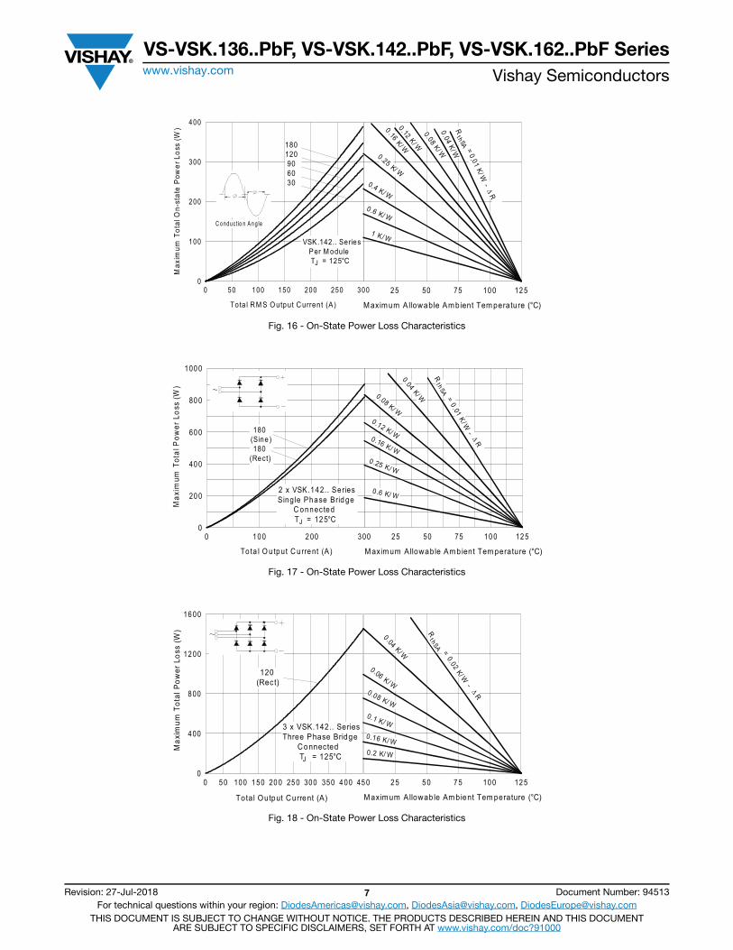
Fig. 16 - On-State Power Loss Characteristics
Fig. 17 - On-State Power Loss Characteristics
Fig. 18 - On-State Power Loss Characteristics
R=
0. 01K/W
-Δ R
0 25 50 75 10 0 12 5
M axim um A llowable Am bient Tem perature (°C)
thSA
0.04K/W
1 K/ W
0.6 K/ W
0.4 K/ W
0.25 K/ W
0.08 K/ W
0.12 K/ W
0 .16K/ W
0
100
200
300
400
0 50 100 150 200 250 300
Tota l RM S O utput C urrent (A)
Max
imum
Tot
al O
n-st
ate
Pow
er L
oss
(W)
C o nduc t io n A n g le
VSK.142.. SeriesPer M oduleT = 125°CJ
180120906030
R
=0.01
K/W-
Δ R
0 25 50 75 10 0 12 5
Maxim um A llowable Am bient Tem perature (°C)
thSA
0.6 K/ W
0.25 K/ W
0.16 K/ W
0.12 K/ W
0.08 K/ W
0.04K/ W
0
20 0
40 0
60 0
80 0
100 0
0 10 0 2 00 300
To ta l O u tput C urre nt (A)
Max
imum
Tot
al P
ower
Los
s (W
)
180(Sine)180
(Rect)
2 x VSK.142.. SeriesSing le Phase Brid ge
C o nnec tedT = 12 5°CJ
0 2 5 5 0 7 5 10 0 12 5
M axim um A llowab le Am bient Tem perature (°C)
R
=0.02
K/ W-
Δ R
t hSA
0.04 K/ W
0.06 K/ W0.08 K/ W
0.1 K/ W
0.16 K/ W0.2 K/ W
0
400
800
12 00
16 00
0 5 0 100 1 50 20 0 25 0 300 350 4 00 45 0
Total Output Current (A)
Max
imum
Tot
al P
ower
Los
s (W
)
120(Rect)
3 x VSK.142.. SeriesThree Phase Bridge
ConnectedT = 125°CJ
VS-VSK.136..PbF, VS-VSK.142..PbF, VS-VSK.162..PbF Serieswww.vishay.com Vishay Semiconductors
Revision: 27-Jul-2018 8 Document Number: 94513For technical questions within your region: [email protected], [email protected], [email protected]
THIS DOCUMENT IS SUBJECT TO CHANGE WITHOUT NOTICE. THE PRODUCTS DESCRIBED HEREIN AND THIS DOCUMENTARE SUBJECT TO SPECIFIC DISCLAIMERS, SET FORTH AT www.vishay.com/doc?91000
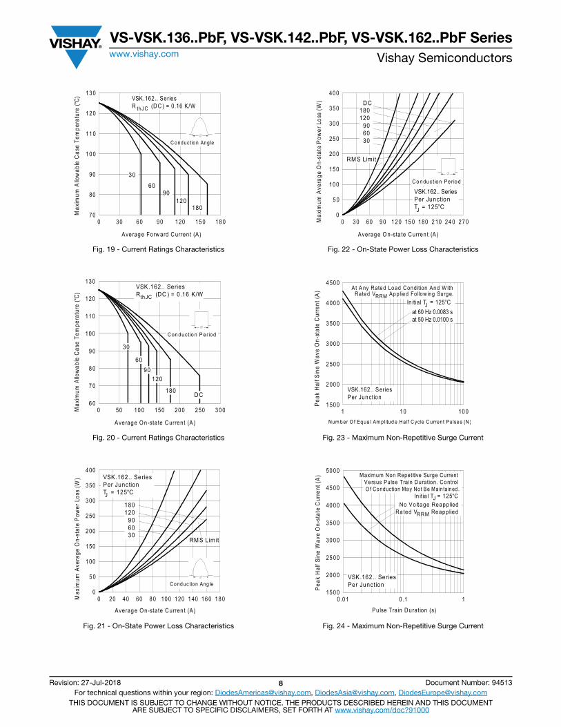
Fig. 19 - Current Ratings Characteristics
Fig. 20 - Current Ratings Characteristics
Fig. 21 - On-State Power Loss Characteristics
Fig. 22 - On-State Power Loss Characteristics
Fig. 23 - Maximum Non-Repetitive Surge Current
Fig. 24 - Maximum Non-Repetitive Surge Current
70
80
90
10 0
11 0
12 0
13 0
0 30 60 90 1 20 15 0 18 0
30
6090
120180
Max
imum
Allo
wab
le C
ase
Tem
pera
ture
(°C)
C onduc tion Angle
Average Fo rw ard C urrent (A)
VSK.162.. SeriesR (D C ) = 0.16 K/WthJC
6 0
7 0
8 0
9 0
100
110
120
130
0 50 10 0 150 20 0 250 30 0
DC
30
6090
120
180
Average O n-sta te C urrent (A)
Max
imum
Allo
wab
le C
ase
Tem
pera
ture
(°C)
Conductio n P er iod
VSK.162.. Series R (DC ) = 0.16 K/WthJC
0
5 0
100
150
200
250
300
350
400
0 20 40 60 8 0 10 0 120 1 40 16 0 18 0
RM S Lim it
C ond uc tion Angle
Max
imum
Ave
rage
On-
stat
e Po
wer
Los
s (W
)
Average O n-state C urren t (A)
VSK.162.. SeriesPer JunctionT = 125°CJ
180120
906030
0
5 0
100
150
200
250
300
350
400
0 30 60 90 1 20 15 0 180 2 10 24 0 27 0
DC180120
906030
RMS Lim it
Co nduc tion Per iod
Max
imum
Ave
rage
On-
stat
e Po
wer
Los
s (W
)
Average O n-sta te C urren t (A )
VSK.162.. SeriesPer JunctionT = 125°CJ
1 500
2 000
2 500
3 000
3 500
4 000
4 500
001011Num ber O f Eq ua l Am p litud e Ha lf C yc le C urrent Pulses (N)
A t A ny Rated Load Condition And W ithRated V App lied Fo llow ing Surge.RRM
Peak
Hal
f Sin
e W
ave
On-
stat
e C
urre
nt (A
)
In it ia l T = 125°Cat 60 Hz 0.0083 sat 50 Hz 0.0100 s
VSK.162.. SeriesPer Jun ction
J
15 00
20 00
25 00
30 00
35 00
40 00
45 00
50 00
11.010.0
Peak
Hal
f Sin
e W
ave
On-
stat
e C
urre
nt (A
)
Pu lse Tra in D uration (s)
Maximum Non Repetitive Surge Current
O f Conduction Ma y No t Be M a inta ined .
VSK.162.. Series Per Junction
In it ia l T = 125°CNo Voltage Reapplied
Rated V ReappliedRRM
Versus Pulse Tra in Duration. Contro l
J
VS-VSK.136..PbF, VS-VSK.142..PbF, VS-VSK.162..PbF Serieswww.vishay.com Vishay Semiconductors
Revision: 27-Jul-2018 9 Document Number: 94513For technical questions within your region: [email protected], [email protected], [email protected]
THIS DOCUMENT IS SUBJECT TO CHANGE WITHOUT NOTICE. THE PRODUCTS DESCRIBED HEREIN AND THIS DOCUMENTARE SUBJECT TO SPECIFIC DISCLAIMERS, SET FORTH AT www.vishay.com/doc?91000
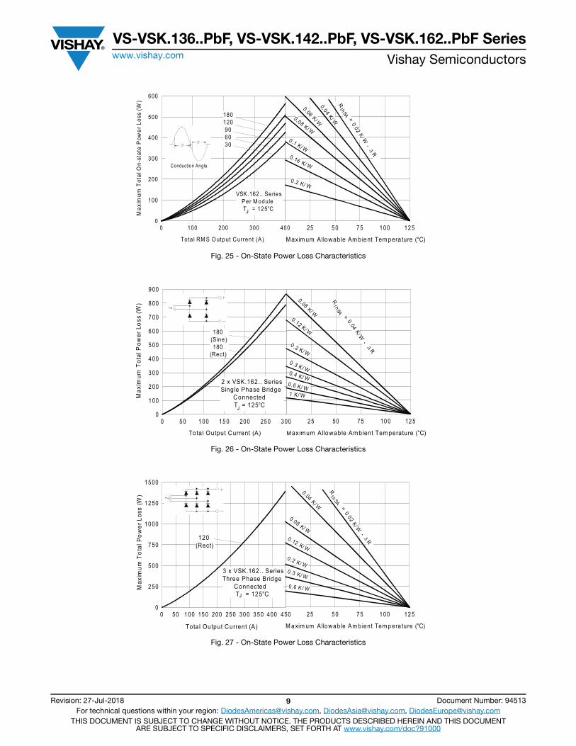
Fig. 25 - On-State Power Loss Characteristics
Fig. 26 - On-State Power Loss Characteristics
Fig. 27 - On-State Power Loss Characteristics
0 25 5 0 7 5 1 00 12 5
Maxim um A llowab le Am bient Tem pera ture (°C)R
=0.02
K/ W-
Δ R
t hSA
0.04K/ W
0.06 K/ W
0.08 K/ W
0.1 K/ W0.16 K/ W
0.2 K/ W
0
100
200
300
400
500
600
0 100 200 300 400
180120906030
Tota l RM S O utput C urrent (A)
Max
imum
Tot
al O
n-st
ate
Pow
er L
oss
(W)
C onductio n Angle
VSK.162.. SeriesPer M oduleT = 125°CJ
R
=0.04
K/ W-
Δ R
0 25 50 75 10 0 12 5
Maxim um A llowable Am bient Tem perature (°C)
t hSA
0.08 K/ W
0.2 K/ W
1 K/ W
0.6 K/ W
0.4 K/ W
0.12 K/ W
0.3 K/ W
0
1 00
2 00
3 00
4 00
5 00
6 00
7 00
8 00
9 00
0 50 1 00 15 0 200 250 300
Tota l Output Current (A)
Max
imum
Tot
al P
ower
Los
s (W
)
2 x VSK.162.. SeriesSingle Phase Bridge
ConnectedT = 125°CJ
180(Sine)180
(Rect)
0 25 5 0 7 5 1 00 12 5
M a xim um Allo w a b le A m b ien t Tem p era tu re (°C)
R
=0.02
K/W-
Δ R
0 .04 K/ W
0 .2 K/ W
0.08 K/ W0 .12 K/ W
0.6 K/ W
0.3 K/ W
thSA
0
2 50
5 00
7 50
10 00
12 50
15 00
0 50 1 00 15 0 200 250 30 0 3 50 400 450
Tota l Output Current (A)
Max
imum
Tot
al P
ower
Los
s (W
)
120(Rect)
3 x VSK.162.. SeriesThree Phase Bridge
ConnectedT = 125°CJ
VS-VSK.136..PbF, VS-VSK.142..PbF, VS-VSK.162..PbF Serieswww.vishay.com Vishay Semiconductors
Revision: 27-Jul-2018 10 Document Number: 94513For technical questions within your region: [email protected], [email protected], [email protected]
THIS DOCUMENT IS SUBJECT TO CHANGE WITHOUT NOTICE. THE PRODUCTS DESCRIBED HEREIN AND THIS DOCUMENTARE SUBJECT TO SPECIFIC DISCLAIMERS, SET FORTH AT www.vishay.com/doc?91000
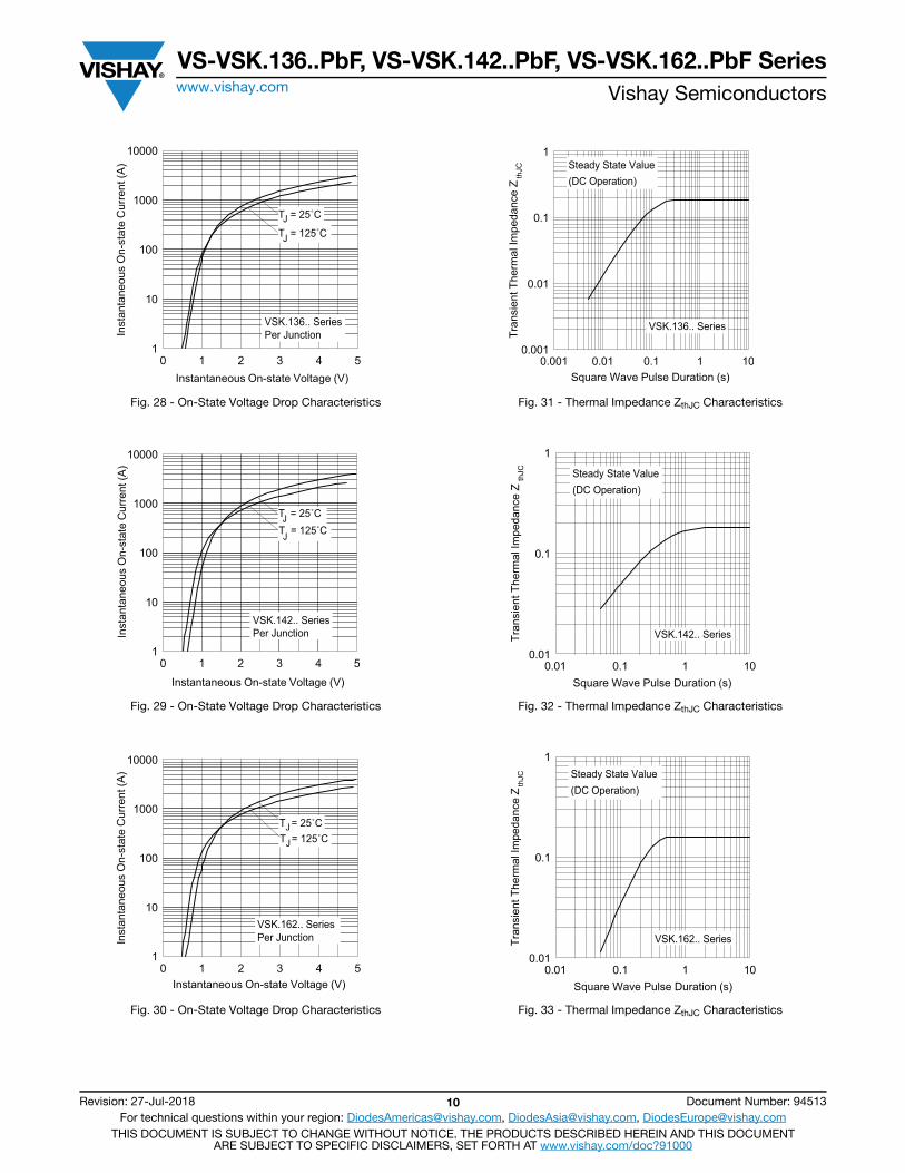
Fig. 28 - On-State Voltage Drop Characteristics
Fig. 29 - On-State Voltage Drop Characteristics
Fig. 30 - On-State Voltage Drop Characteristics
Fig. 31 - Thermal Impedance ZthJC Characteristics
Fig. 32 - Thermal Impedance ZthJC Characteristics
Fig. 33 - Thermal Impedance ZthJC Characteristics
Instantaneous On-state Voltage (V)
Inst
anta
neou
s O
n-st
ate
Cur
rent
(A)
1
10
100
1000
10000
0 1 2 3 4 5
T = 25˚CJT = 125˚C
VSK.136.. SeriesPer Junction
J
Instantaneous On-state Voltage (V)
Inst
anta
neou
s O
n-st
ate
Cur
rent
(A)
1
10
100
1000
10000
0 1 2 3 4 5
T = 125˚CT = 25˚C
VSK.142.. SeriesPer Junction
J
J
1
10
100
1000
10000
0 1 2 3 4 5
T = 25˚CJT = 125˚C
VSK.162.. SeriesPer Junction
J
Instantaneous On-state Voltage (V)
Inst
anta
neou
s O
n-st
ate
Cur
rent
(A)
Square Wave Pulse Duration (s)
Tran
sien
t The
rmal
Impe
danc
e Z
thJC
0.001
0.01
0.1
1
0.001 0.01 0.1 1 10
Steady State Value(DC Operation)
VSK.136.. Series
Square Wave Pulse Duration (s)
Tran
sien
t The
rmal
Impe
danc
e Z
thJC
0.01
0.1
1
0.01 0.1 1 10
Steady State Value(DC Operation)
VSK.142.. Series
Square Wave Pulse Duration (s)
Tran
sien
t The
rmal
Impe
danc
e Z
thJC
0.01
0.1
1
0.01 0.1 1 10
Steady State Value(DC Operation)
VSK.162.. Series
VS-VSK.136..PbF, VS-VSK.142..PbF, VS-VSK.162..PbF Serieswww.vishay.com Vishay Semiconductors
Revision: 27-Jul-2018 11 Document Number: 94513For technical questions within your region: [email protected], [email protected], [email protected]
THIS DOCUMENT IS SUBJECT TO CHANGE WITHOUT NOTICE. THE PRODUCTS DESCRIBED HEREIN AND THIS DOCUMENTARE SUBJECT TO SPECIFIC DISCLAIMERS, SET FORTH AT www.vishay.com/doc?91000
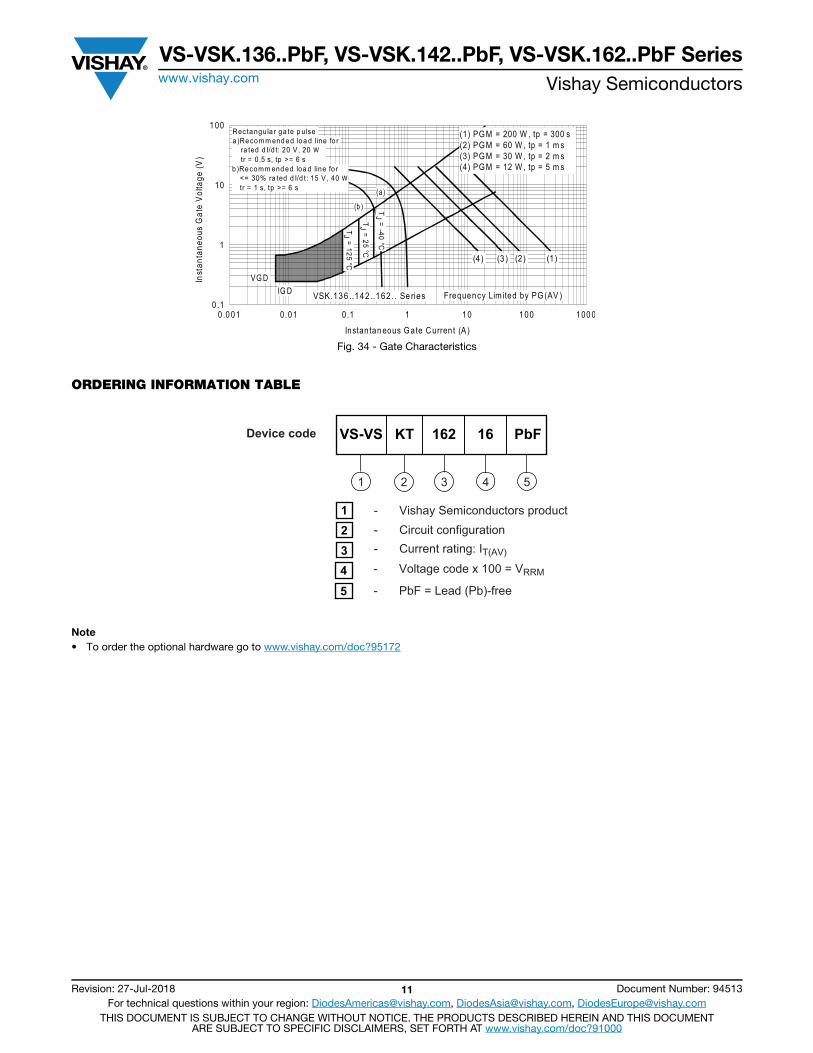
Fig. 34 - Gate Characteristics
ORDERING INFORMATION TABLE
Note• To order the optional hardware go to www.vishay.com/doc?95172
0 .1
1
10
1 00
0 .0 01 0.01 0 .1 1 1 0 1 00 100 0
(b )
(a )
Rec ta ngula r ga te p ulse
(4) (3 ) (2) (1)
Inst
anta
neou
s G
ate
Volta
ge (V
)
TJ = -40 °C
TJ = 25 °C
TJ = 125 °C
a )Recom m end ed loa d l ine fo r
b )Recom m end ed loa d line fo r
VG DIG D
(1) PG M = 200 W , tp = 300 s(2) PG M = 60 W , tp = 1 m s(3) PG M = 30 W , tp = 2 m s(4) PG M = 12 W , tp = 5 m s
<= 30% ra ted d I/d t: 15 V , 40 Wtr = 1 s, tp >= 6 s
ra ted d I/d t: 20 V, 20 Wtr = 0.5 s, tp >= 6 s
VSK.136 ..142..162.. Se ries Frequency Lim ited by PG (AV )
Instan tan eous G ate C urren t (A )
12 - Circuit configuration
3 - Current rating: IT(AV)
4 - Voltage code x 100 = VRRM
5 - PbF = Lead (Pb)-free
Device code
51 32 4
VS-VS 16 PbFKT 162
- Vishay Semiconductors product
VS-VSK.136..PbF, VS-VSK.142..PbF, VS-VSK.162..PbF Serieswww.vishay.com Vishay Semiconductors
Revision: 27-Jul-2018 12 Document Number: 94513For technical questions within your region: [email protected], [email protected], [email protected]
THIS DOCUMENT IS SUBJECT TO CHANGE WITHOUT NOTICE. THE PRODUCTS DESCRIBED HEREIN AND THIS DOCUMENTARE SUBJECT TO SPECIFIC DISCLAIMERS, SET FORTH AT www.vishay.com/doc?91000
CIRCUIT CONFIGURATION
CIRCUIT DESCRIPTION CIRCUITCONFIGURATION CODE CIRCUIT DRAWING
Two SCRs doubler circuit T
SCR/diode doubler circuit, positive control H
SCR/diode doubler circuit, negative control L
LINKS TO RELATED DOCUMENTS
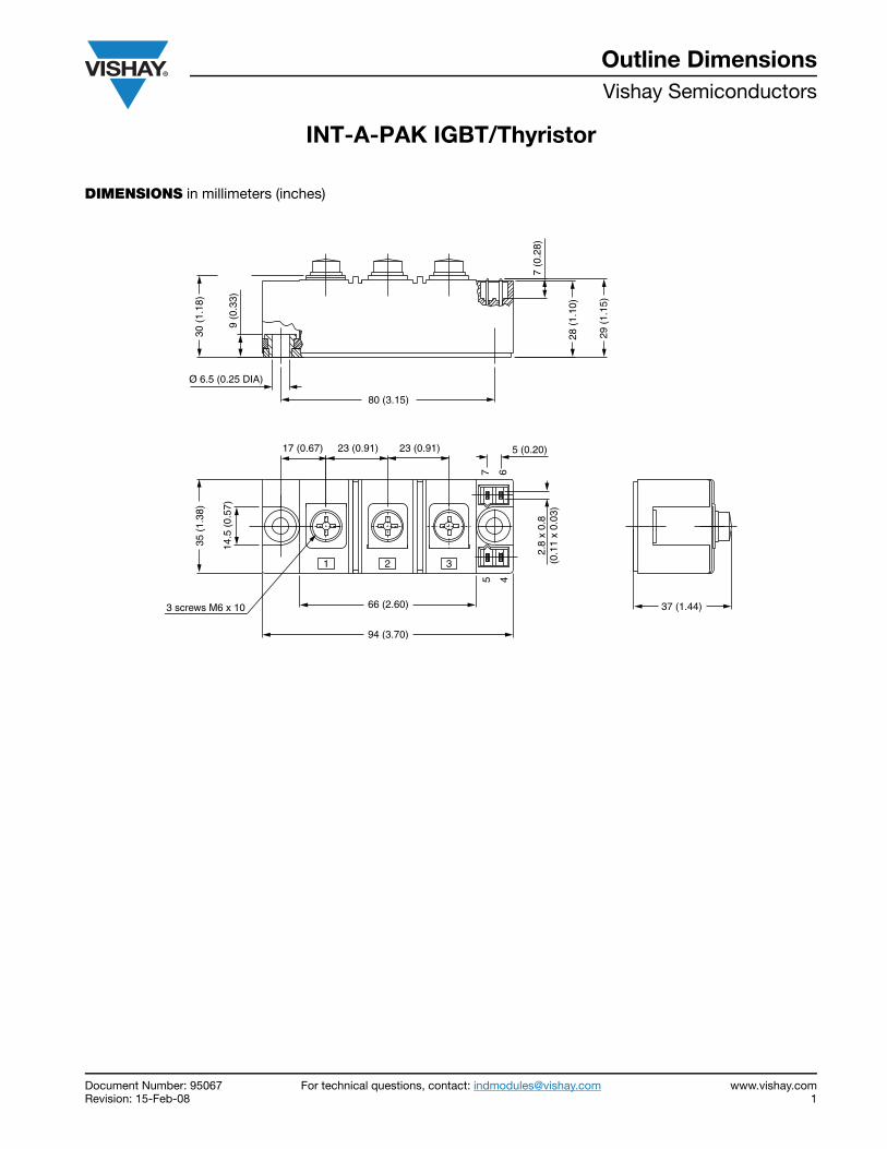
Dimensions www.vishay.com/doc?95067
-
+
~
K1 K2
G1 G2
-
+
VSKT...
-
+
~
K1G1
-
+
VSKH...
-
+
VSKL...
-
+
~
K2G2
Document Number: 95067 For technical questions, contact: [email protected] www.vishay.comRevision: 15-Feb-08 1
INT-A-PAK IGBT/Thyristor
Outline DimensionsVishay Semiconductors
DIMENSIONS in millimeters (inches)
80 (3.15)
Ø 6.5 (0.25 DIA)
30 (
1.18
)
9 (0
.33)
7 (0
.28)
28 (
1.10
)
29 (
1.15
)37 (1.44)
5 (0.20)
2.8
x 0.
8(0
.11
x 0.
03)
7 6
5 4
1 2 3
23 (0.91)23 (0.91)17 (0.67)
35 (
1.38
)
14.5
(0.
57)
3 screws M6 x 10 66 (2.60)
94 (3.70)
Legal Disclaimer Noticewww.vishay.com Vishay
Revision: 08-Feb-17 1 Document Number: 91000
DisclaimerALL PRODUCT, PRODUCT SPECIFICATIONS AND DATA ARE SUBJECT TO CHANGE WITHOUT NOTICE TO IMPROVE RELIABILITY, FUNCTION OR DESIGN OR OTHERWISE.
Vishay Intertechnology, Inc., its affiliates, agents, and employees, and all persons acting on its or their behalf (collectively, “Vishay”), disclaim any and all liability for any errors, inaccuracies or incompleteness contained in any datasheet or in any other disclosure relating to any product.
Vishay makes no warranty, representation or guarantee regarding the suitability of the products for any particular purpose or the continuing production of any product. To the maximum extent permitted by applicable law, Vishay disclaims (i) any and all liability arising out of the application or use of any product, (ii) any and all liability, including without limitation special, consequential or incidental damages, and (iii) any and all implied warranties, including warranties of fitness for particular purpose, non-infringement and merchantability.
Statements regarding the suitability of products for certain types of applications are based on Vishay’s knowledge of typical requirements that are often placed on Vishay products in generic applications. Such statements are not binding statements about the suitability of products for a particular application. It is the customer’s responsibility to validate that a particular product with the properties described in the product specification is suitable for use in a particular application. Parameters provided in datasheets and / or specifications may vary in different applications and performance may vary over time. All operating parameters, including typical parameters, must be validated for each customer application by the customer’s technical experts. Product specifications do not expand or otherwise modify Vishay’s terms and conditions of purchase, including but not limited to the warranty expressed therein.
Except as expressly indicated in writing, Vishay products are not designed for use in medical, life-saving, or life-sustaining applications or for any other application in which the failure of the Vishay product could result in personal injury or death. Customers using or selling Vishay products not expressly indicated for use in such applications do so at their own risk. Please contact authorized Vishay personnel to obtain written terms and conditions regarding products designed for such applications.
No license, express or implied, by estoppel or otherwise, to any intellectual property rights is granted by this document or by any conduct of Vishay. Product names and markings noted herein may be trademarks of their respective owners.
© 2017 VISHAY INTERTECHNOLOGY, INC. ALL RIGHTS RESERVED