VOLUME NINETY TWO - CASVOLUME NINETY TWO SEMICONDUCTORS AND SEMIMETALS Advances in Photovoltaics:...
192
Transcript of VOLUME NINETY TWO - CASVOLUME NINETY TWO SEMICONDUCTORS AND SEMIMETALS Advances in Photovoltaics:...

VOLUME NINETY TWO
SEMICONDUCTORS ANDSEMIMETALSAdvances in Photovoltaics: Part 4
SERIES EDITORSEICKE R. WEBERDirectorFraunhofer-Institutf€ur Solare Energiesysteme ISEVorsitzender, Fraunhofer-Allianz EnergieHeidenhofstr. 2, 79110Freiburg, Germany
CHENNUPATI JAGADISHAustralian Laureate Fellowand Distinguished ProfessorDepartment of ElectronicMaterials EngineeringResearch School of Physicsand EngineeringAustralian National UniversityCanberra, ACT 0200Australia
VOLUME NINETY TWO
SEMICONDUCTORS ANDSEMIMETALSAdvances in Photovoltaics: Part 4
Edited by
GERHARD P. WILLEKEFraunhofer-Institut f€ur SolareHeidenhofstr. 2, 79110Freiburg, Germany
EICKE R. WEBERFraunhofer-Institutf€ur Solare Energiesysteme ISEVorsitzender, Fraunhofer-Allianz EnergieHeidenhofstr. 2, 79110Freiburg, Germany
AMSTERDAM • BOSTON • HEIDELBERG • LONDONNEW YORK • OXFORD • PARIS • SAN DIEGO
SAN FRANCISCO • SINGAPORE • SYDNEY • TOKYOAcademic Press is an imprint of Elsevier
Academic Press is an imprint of Elsevier
225 Wyman Street, Waltham, MA 02451, USA
525 B Street, Suite 1800, San Diego, CA 92101-4495, USA
125 London Wall, London, EC2Y 5AS, UK
The Boulevard, Langford Lane, Kidlington, Oxford OX5 1GB, UK
First edition 2015
© 2015 Elsevier Inc. All rights reserved
No part of this publication may be reproduced or transmitted in any form or by any means,
electronic or mechanical, including photocopying, recording, or any information storage and
retrieval system, without permission in writing from the publisher. Details on how to seek
permission, further information about the Publisher’s permissions policies and our
arrangements with organizations such as the Copyright Clearance Center and the Copyright
Licensing Agency, can be found at our website: www.elsevier.com/permissions.
This book and the individual contributions contained in it are protected under copyright by
the Publisher (other than as may be noted herein).
Notices
Knowledge and best practice in this field are constantly changing. As new research and
experience broaden our understanding, changes in research methods, professional practices,
or medical treatment may become necessary.
Practitioners and researchers must always rely on their own experience and knowledge in
evaluating and using any information, methods, compounds, or experiments described
herein. In using such information or methods they should be mindful of their own safety and
the safety of others, including parties for whom they have a professional responsibility.
To the fullest extent of the law, neither the Publisher nor the authors, contributors, or editors,
assume any liability for any injury and/or damage to persons or property as a matter of
products liability, negligence or otherwise, or from any use or operation of any methods,
products, instructions, or ideas contained in the material herein.
ISBN: 978-0-12-801021-1
ISSN: 0080-8784
For information on all Academic Press publications
visit our website at store.elsevier.com
CONTENTS
Contributors vii
Preface ix
1. Silicon Crystallization Technologies 1
Peter Dold
1. Silicon Feedstock 1
2. Fundamental Parameters for Silicon Crystallization 12
3. Crystallization Technologies 19
4. Summary and Final Remarks 54
References 56
2. Wafering of Silicon 63
Hans Joachim M€oller
1. Introduction 63
2. Multiwire Sawing Technology 65
3. Basic Sawing Mechanisms 90
4. Alternative Wafering Technologies 102
References 105
3. Reliability Issues of CIGS-Based Thin Film Solar Cells 111
Thomas Walter
1. Reliability 111
2. Metastabilities 115
3. Partial Shading and Hotspots 117
4. Potential-Induced Degradation 132
5. Back Contact 138
References 148
Index 151
Contents of Volumes in this Series 155
v

This page intentionally left blank

CONTRIBUTORS
Peter Dold
Fraunhofer CSP, Halle, Germany. (ch1)
Hans Joachim M€ollerFraunhofer Technology Center for Semiconductor Materials, Freiberg, Germany. (ch2)
Thomas Walter
Faculty of Mechatronics and Medical Engineering, University of Applied Sciences Ulm,
Ulm, Germany. (ch3)
vii

This page intentionally left blank
PREFACE
The rapid transformation of our energy supply system to the more efficient
use of increasingly renewable energies is one of the biggest challenges and
opportunities of the present century. Harvesting solar energy by photovol-
taics is considered to be a cornerstone technology for this truly global trans-
formation process, and it is well on its way. The speed of progress is
illustrated by looking at some figures of the cumulative installed PV peak
power capacity. In Part 1 of this series of “Advances of Photovoltaics,”
published in 2012, the introduction mentioned 70 GWp installed at the
end of 2011. As we write this preface of Part 4 in the spring of 2015, 1%
of the world electricity generation is now already supplied by PV, and in
the coming months the global PV installation figure will have tripled
compared with 2011! But this is just the beginning of the thousands of
GWp that are likely to be installed in the decades to come.
Key for this extraordinary development was the rapid decrease of PV
prices and thus the cost of solar electricity. This was fueled by a rapid
technology development with soaring efficiencies at reduced production
cost, coupled with an effective market introduction policy, especially the
well-designed German feed-in tariff. Today, we can harvest solar electricity
even in Germany—with insolation comparable to Alaska!—for about
10$ct/kWh, and in sun-rich areas for half of this amount, far below the cost,
e.g., electricity obtained from Diesel generators.
As already mentioned above, this book presents the fourth volume in the
ongoing series “Advances in Photovoltaics” within Semiconductors and
Semimetals. This series has been designed to provide a thorough overview
of the underlying physics, the important materials aspects, the prevailing and
future solar cell design issues, production technologies, as well as energy sys-
tem integration and characterization issues. The present volume deals with
three important issues, of crystallizing silicon, the dominating PV material,
the ways of how to transform it into wafers for solar cells, as well as the issue
of reliability of CIGS-based thin film solar cells and modules. Following the
tradition of this series, all chapters are written by world-leading experts in
their respective field.
As we write this text, the German PV market is likely to collapse from a
7.5 GWp/a market as recently as 2012 to a 1 GWp/a level in 2015, a market
size that we last had in 2007. Fortunately, other markets in China, Japan, and
ix

the USA are now taking over by currently developing into 10 GWp per year
and more markets.
The solar PV revolution has started irreversibly, it is now fueled by
economics in addition to the concern for reducing climate gas emissions,
and it takes rapid foothold beyond Europe in Asia and the Americas, the
other parts of our planet will follow in a few year’s time!
GERHARD P. WILLEKE AND EICKE R. WEBER
Fraunhofer ISE, Freiburg, Germany
x Preface

CHAPTER ONE
Silicon CrystallizationTechnologiesPeter Dold1Fraunhofer CSP, Halle, Germany1Corresponding author: e-mail address: [email protected]
Contents
1. Silicon Feedstock 11.1 Polysilicon: The Base Material for over 90% of All Solar Cells 11.2 The Chemical Path 31.3 Fluidized Bed Reactor 61.4 The Metallurgical Path: UMG-Si 91.5 Different Poly for Different Crystallization Techniques 11
2. Fundamental Parameters for Silicon Crystallization 122.1 Material Properties, Material Utilization, and Chemical Reactivity 122.2 Numerical Simulation 18
3. Crystallization Technologies 193.1 Pulling from the Melt: The Cz Technique 203.2 Directional Solidification: Growth of Multicrystalline Silicon 363.3 FZ Growth 45
4. Summary and Final Remarks 54References 56
1. SILICON FEEDSTOCK
1.1 Polysilicon: The Base Material for over 90% of AllSolar Cells
The roller coaster ride of the polysilicon industry during the last 10 years was
quite extraordinary—even compared with the ups and downs of the semi-
conductor business over the last half century. The golden age of polysilicon
in the years 2007–2010, when companies could make billions of dollars if
they were able to deliver polysilicon at all, was followed by the severe crush
in the years 2011–2012, when most of the newcomers marched into bank-
ruptcy and disappeared. And, even some of the old ones had to fight heavily
Semiconductors and Semimetals, Volume 92 # 2015 Elsevier Inc.ISSN 0080-8784 All rights reserved.http://dx.doi.org/10.1016/bs.semsem.2015.04.001
1
to survive. During the golden years, spot market prices had reached highs of
200–300 or even 400 US$/kg polysilicon, simply because the market was
swept and the order books of the cell and module manufacturers were full.
The polysilicon industry was not prepared for such a fast ramp-up, invest-
ment is high,1 and equipment could not readily be ordered. The long-
established companies either have an exclusive partnership with a specific
equipment manufacturer, or they make the equipment in-house. Produc-
tion capacity could not easily be ramped up, but once the train was running,
it also could not be stopped so easily and could not be adjusted to the then
changed market situation, partly because typical polysilicon projects take
several years from the financing phase all the way up to full production,
and partly because the players did not want to believe that the silicon
bonanza was over. The huge shortage was followed by a tremendous over
supply with spot market prices as low as 14–16 US$/kg in 2013—which was
below the actual production costs. Today, spot market prices leveled off
around 17–18 US$/kg and no significant changes are expected for the near
future.
As a consequence, all (or at least as good as all) of the new and innovative
approaches for polysilicon refinement, for upgrading metallurgical silicon
(an excellent review was given by Heuer, 2013), or for alternative produc-
tion methods (compare Bernreuter and Haugwitz, 2010) could not find a
market share and disappeared again. The traditional Chemical Vapor Depo-
sition (CVD)-based Siemens process (Fabry and Hesse, 2012), probably not
the most sophisticated technology for solar-grade-silicon production—but
for sure the most matured technique, was the match winner. A good over-
view of the market situation and an in-depth analysis of the trends are given
by Bernreuter every first or second year (Bernreuter, 2014).
Basically, two main routes might be distinguished for the refinement of
polysilicon: (I) the chemical path: bringing silicon into the gas phase and
purifying it by distillation, followed by thermal pyrolysis of the gaseous spe-
cies; and (II) the metallurgical path, where impurities are removed from sil-
icon by mixing it with another metal or with a slag, then let the impurities
segregate into the second phase, separate the different phases somehow
mechanically, and clean the surface of the silicon crystallites by chemical
etching.
1 Back in 2008, a polysilicon plant with a capacity of 10,000 t/a required an investment of at least 1 bil-
lion US$. Today, it might be something in the range of 400–600 M$, depending on the location.
2 Peter Dold
1.2 The Chemical PathThe Siemens process (or modified Siemens process, as many manufacturers
like to call their variation) allows to produce ultrapure polysilicon, with
metallic bulk impurity levels as low as a few tens of ppt (parts per trillion)
or an equivalent of 10–11N. Electrically active elements (donors, acceptors)
are in the ppt range and only carbon and oxygen show up in higher concen-
trations, where lower single-digit parts per million levels are found. For
semiconductor applications, there is no alternative so far to the polysilicon
produced by the Siemens process.
The Siemens process itself goes back to a patent in the late 1950s filed by
the German electronics company Siemens (Reuschel, 1963; Schweickert
et al., 1961), which stepped out of the polysilicon business long ago. It
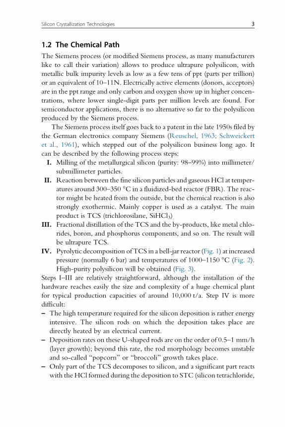
can be described by the following process steps:
I. Milling of the metallurgical silicon (purity: 98–99%) into millimeter/
submillimeter particles.
II. Reaction between the fine silicon particles and gaseous HCl at temper-
atures around 300–350 °C in a fluidized-bed reactor (FBR). The reac-
tor might be heated from the outside, but the chemical reaction is also
strongly exothermic. Mainly copper is used as a catalyst. The main
product is TCS (trichlorosilane, SiHCl3).III. Fractional distillation of the TCS and the by-products, like metal chlo-
rides, boron, and phosphorus components, and so on. The result will
be ultrapure TCS.
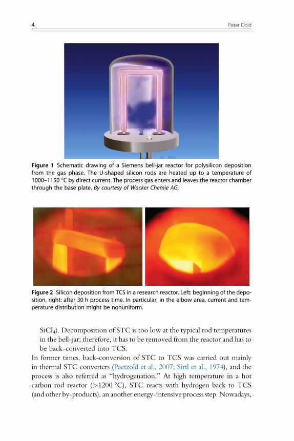
IV. Pyrolytic decomposition of TCS in a bell-jar reactor (Fig. 1) at increased
pressure (normally 6 bar) and temperatures of 1000–1150 °C (Fig. 2).
High-purity polysilicon will be obtained (Fig. 3).
Steps I–III are relatively straightforward, although the installation of the
hardware reaches easily the size and complexity of a huge chemical plant
for typical production capacities of around 10,000 t/a. Step IV is more
difficult:
– The high temperature required for the silicon deposition is rather energy
intensive. The silicon rods on which the deposition takes place are
directly heated by an electrical current.
– Deposition rates on these U-shaped rods are on the order of 0.5–1 mm/h
(layer growth); beyond this rate, the rod morphology becomes unstable
and so-called “popcorn” or “broccoli” growth takes place.
– Only part of the TCS decomposes to silicon, and a significant part reacts
with the HCl formed during the deposition to STC (silicon tetrachloride,
3Silicon Crystallization Technologies
SiCl4). Decomposition of STC is too low at the typical rod temperatures
in the bell-jar; therefore, it has to be removed from the reactor and has to
be back-converted into TCS.
In former times, back-conversion of STC to TCS was carried out mainly
in thermal STC converters (Paetzold et al., 2007; Sirtl et al., 1974), and the
process is also referred as “hydrogenation.” At high temperature in a hot
carbon rod reactor (>1200 °C), STC reacts with hydrogen back to TCS
(and other by-products), an another energy-intensive process step. Nowadays,
Figure 1 Schematic drawing of a Siemens bell-jar reactor for polysilicon depositionfrom the gas phase. The U-shaped silicon rods are heated up to a temperature of1000–1150 °C by direct current. The process gas enters and leaves the reactor chamberthrough the base plate. By courtesy of Wacker Chemie AG.
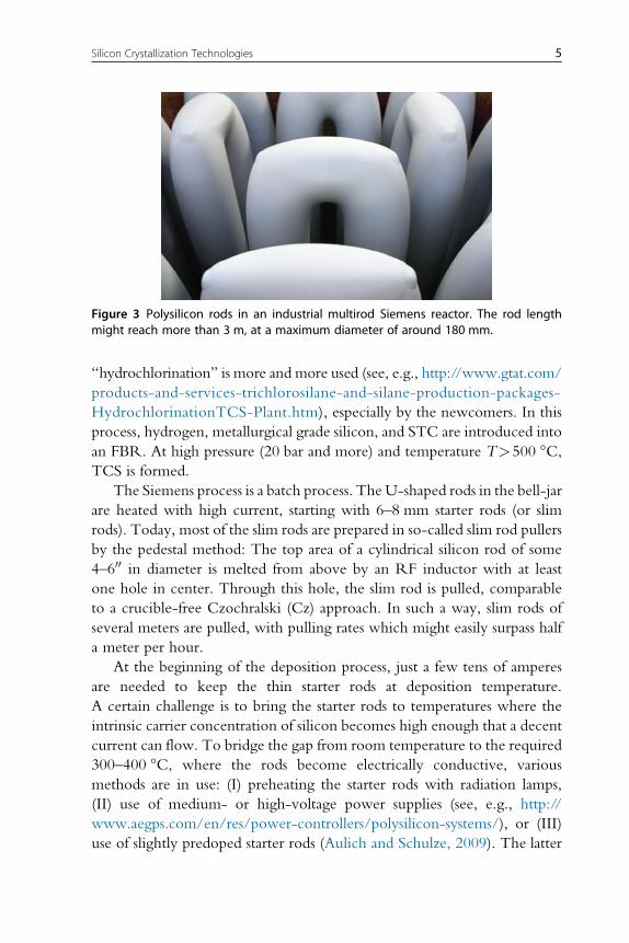
Figure 2 Silicon deposition from TCS in a research reactor. Left: beginning of the depo-sition, right: after 30 h process time. In particular, in the elbow area, current and tem-perature distribution might be nonuniform.
4 Peter Dold
“hydrochlorination” is more and more used (see, e.g., http://www.gtat.com/
products-and-services-trichlorosilane-and-silane-production-packages-
HydrochlorinationTCS-Plant.htm), especially by the newcomers. In this
process, hydrogen, metallurgical grade silicon, and STC are introduced into
an FBR. At high pressure (20 bar and more) and temperature T>500 °C,TCS is formed.
The Siemens process is a batch process. TheU-shaped rods in the bell-jar
are heated with high current, starting with 6–8 mm starter rods (or slim
rods). Today, most of the slim rods are prepared in so-called slim rod pullers
by the pedestal method: The top area of a cylindrical silicon rod of some
4–600 in diameter is melted from above by an RF inductor with at least
one hole in center. Through this hole, the slim rod is pulled, comparable
to a crucible-free Czochralski (Cz) approach. In such a way, slim rods of
several meters are pulled, with pulling rates which might easily surpass half
a meter per hour.
At the beginning of the deposition process, just a few tens of amperes
are needed to keep the thin starter rods at deposition temperature.
A certain challenge is to bring the starter rods to temperatures where the
intrinsic carrier concentration of silicon becomes high enough that a decent
current can flow. To bridge the gap from room temperature to the required
300–400 °C, where the rods become electrically conductive, various
methods are in use: (I) preheating the starter rods with radiation lamps,
(II) use of medium- or high-voltage power supplies (see, e.g., http://
www.aegps.com/en/res/power-controllers/polysilicon-systems/), or (III)
use of slightly predoped starter rods (Aulich and Schulze, 2009). The latter
Figure 3 Polysilicon rods in an industrial multirod Siemens reactor. The rod lengthmight reach more than 3 m, at a maximum diameter of around 180 mm.
5Silicon Crystallization Technologies

is not an option for electronic grade material, but quite an option for solar-
grade polysilicon. At the end of the process cycle,when the rods have reached
their final size of 150–180 mm in diameter, several thousand amperes are
required to keep them at the specific deposition temperature. The whole
cycle takes about 100 h, depending on the deposition rates and the final size.
The maximum diameter is limited by the temperature gradient between the
rod surface (which has to stay around 1100 °Candwhich cools downby radi-
ation and by convection) and the hotter core of the rod, where the current
flows preferentially. If the core or the elbow areas become too hot, there is a
risk that the silicon is melting, which results in a strong decrease of the elec-
trical resistivity, and finally a local shortcut and a burned-through rod.
Some 10 years ago, with lower deposition rates, smaller reactors, and
less-optimized processes, power consumption to produce 1 kg of silicon
was in the range of 150–200 kWh/kg (including STC conversion). Today,
state-of-the-art reactors with some 48–72 rods (even 96 rod reactors are on
the market), and an annual capacity of some 400 t of silicon, high deposition
rates, integrated hydrochlorination, and proper debottlenecking, the power
consumption is as low as 50–70 kWh/kg. Some manufacturers are claiming
that they can even reach values below 50 kWh/kg.
As already mentioned in the beginning, the Siemens process is now very
matured, which also means that we cannot expect huge progress steps any-
more, and further improvements will be rather incremental and less revolu-
tionary. A significant cost reduction is promised by the FBR technology.
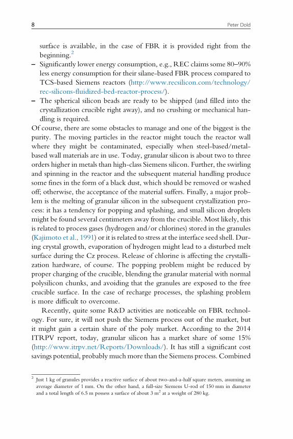
1.3 Fluidized Bed ReactorIn contrast to the batch-type Siemens process, the FBR operates in a con-
tinuous mode. Small seed particles (high-purity silicon with diameters of
some tens of micrometers) are fed into a heated reactor, a strong gas flow
(either TCS or silane, mixed with hydrogen) from the bottom part of the
reactor keeps the particles floating (Fig. 4). An excellent overview was given
in Ydstie and Du (2011). Reaction with TCS (or silane as used in the case of
the company REC) lets the silicon particles grow, until they reach a critical
mass and sink to the bottom area in the form of granules (or beads; Fig. 5),
where they can be harvested easily. The technology has a certain charm and
several advantages are obvious:
– Continuous operation—minimized downtime.
– High deposition rates due to a large silicon surface; different to the Sie-
mens process where only toward the end of the process a large deposition
6 Peter Dold
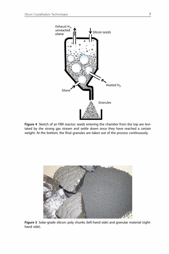
Figure 4 Sketch of an FBR reactor: seeds entering the chamber from the top are levi-tated by the strong gas stream and settle down once they have reached a certainweight. At the bottom, the final granules are taken out of the process continuously.
Figure 5 Solar-grade silicon: poly chunks (left-hand side) and granular material (right-hand side).
7Silicon Crystallization Technologies
surface is available, in the case of FBR it is provided right from the
beginning.2
– Significantly lower energy consumption, e.g., REC claims some 80–90%
less energy consumption for their silane-based FBR process compared to
TCS-based Siemens reactors (http://www.recsilicon.com/technology/
rec-silicons-fluidized-bed-reactor-process/).
– The spherical silicon beads are ready to be shipped (and filled into the
crystallization crucible right away), and no crushing or mechanical han-
dling is required.
Of course, there are some obstacles to manage and one of the biggest is the
purity. The moving particles in the reactor might touch the reactor wall
where they might be contaminated, especially when steel-based/metal-
based wall materials are in use. Today, granular silicon is about two to three
orders higher in metals than high-class Siemens silicon. Further, the swirling
and spinning in the reactor and the subsequent material handling produce
some fines in the form of a black dust, which should be removed or washed
off; otherwise, the acceptance of the material suffers. Finally, a major prob-
lem is the melting of granular silicon in the subsequent crystallization pro-
cess: it has a tendency for popping and splashing, and small silicon droplets
might be found several centimeters away from the crucible. Most likely, this
is related to process gases (hydrogen and/or chlorines) stored in the granules
(Kajimoto et al., 1991) or it is related to stress at the interface seed shell. Dur-
ing crystal growth, evaporation of hydrogen might lead to a disturbed melt
surface during the Cz process. Release of chlorine is affecting the crystalli-
zation hardware, of course. The popping problem might be reduced by
proper charging of the crucible, blending the granular material with normal
polysilicon chunks, and avoiding that the granules are exposed to the free
crucible surface. In the case of recharge processes, the splashing problem
is more difficult to overcome.
Recently, quite some R&D activities are noticeable on FBR technol-
ogy. For sure, it will not push the Siemens process out of the market, but
it might gain a certain share of the poly market. According to the 2014
ITRPV report, today, granular silicon has a market share of some 15%
(http://www.itrpv.net/Reports/Downloads/). It has still a significant cost
savings potential, probably muchmore than the Siemens process. Combined
2 Just 1 kg of granules provides a reactive surface of about two-and-a-half square meters, assuming an
average diameter of 1 mm. On the other hand, a full-size Siemens U-rod of 150 mm in diameter
and a total length of 6.5 m possess a surface of about 3 m2 at a weight of 280 kg.
8 Peter Dold
with broken poly chunks from Siemens reactors, an improved crucible fill
factor is achieved, an improvement of 29.3% was reported (REC Silicon
Inc., 2013), the small granules fill perfectly the space between the larger
chunks, and, the filling of crucibles with granules is fast.
1.4 The Metallurgical Path: UMG-SiOver many years, photovoltaic industry (PV) used the leftovers from the
semiconductor industry, which was in most cases ultrapure poly-feedstock,
cutoffs fromCz ingots, and so on. The base material was in the range of 9–10
or even 11N purity. Using it for multicrystalline ingots, there is hardly any
difference noticeable whether 6N or 8N or 10N polysilicon is used. There-
fore, the question seemed appropriate: Why not use silicon of purity just
clean enough for cell processes and simplify the purification process accord-
ingly? The metallurgical path seemed highly promising: easy to scale,
low-energy consumption, low Capital Expenditures (CAPEX)—but still
delivering a fully usable product. Dozens and dozens of groups and compa-
nies tried it worldwide (Bernreuter and Haugwitz, 2010), and only about
two survived on a scale somewhere between pilot and full production:
Silicor Materials and Elkem (a subsidiary of China National Bluestar Group
Co. Ltd.). The U.S.-based company Silicor Materials (former Calisolar) had
purchased the UMG-process from the Canadian company 6N. The 6N pro-
cess (Nichol, 2011) is based on the alloying of silicon with aluminum3: Met-
allurgical grade silicon of some 98–99% purity is mixed with aluminum, and
the hypoeutectic mixture becomes liquid in the range of 900–1000 °C,depending on the silicon concentration. The eutectic temperature itself is
577 °C, with a silicon concentration of 12.2 at%. Cooling down the hypo-
eutectic mix, the excess silicon forms small crystallites or flakes, embedded in
the liquid Al–Si melt. In silicon, all metals show small segregation coeffi-
cients4 and, consequently, are enriched in the melt, or better, are accumu-
lated in the solid–liquid boundary layer. The point with the accumulation
within the boundary layer is a bit problematic: a proper separation of the
silicon crystallites from the melt is essential and a chemical etching step is
required to dissolve the metals. To get a good cost structure, the residual
3 Instead of aluminum, tin would also be an option, but aluminum can be separated from silicon more
easily, either mechanically (e.g., centrifugation) or chemically etched off. Basically, all materials used in
former times for the liquid-phase epitaxy (LPE) of silicon could be used for alloying with silicon;
restrictions result mainly from practical considerations like availability in large quantities and price.4 The lower temperature of the Al–Si melt compared to pure liquid silicon reduces the segregation coef-
ficients even further (e.g., Morita and Yoshikawa, 2011).
9Silicon Crystallization Technologies
Al–Si melt—still slightly hypoeutectic—has to be sold, but there is a market
for this kind of alloys. The main trouble makers are, besides the proper
removal of the aluminum, which might be trapped in inclusions, the elim-
ination or reduction of boron and phosphorus. Recently, plans for a 16,000 t
plant in Island had been released (Kaes et al., 2014).
Core features of the ELKEM process are chemical etching and slag treat-
ment (Ceccaroli and Friestad, 2005; Heuer, 2013; Schei, 1998; Wang et al.,
2014). A calcium-based slag is used, and during the cooling-down phase,
most of the impurities are accumulated in the slag. After solidification,
the slag and the impurities are etched off and purified silicon is obtained.
The process works very well for the metallic impurities, but again, boron
and phosphorus are still present and the material is somewhat compensated.
Boron and phosphorus had been the greatest bottleneck for all the dif-
ferent UMG processes or better: their issue of failure. Boron shows a segre-
gation coefficient of k0¼0.8 (somewhat lower at reduced temperatures) and
phosphorus 0.35. Removing boron and phosphorus simply by segregation is
not an option. All the methods developed so far are either costly or compli-
cated (or both):
– oxidizing the boron out (the Becancour/Timminco process): huge loss of
silicon (Leblanc and Boisvert, 2008).
– removing it by slagging: expensive and risk of introducing other impu-
rities (Ceccaroli and Friestad, 2005; Schei, 1998; Wang et al., 2014).
– gettering, forming a metal boride (e.g., TiB2): not efficient enough
(Yoshikawa et al., 2005).
– using low boron raw materials (SolSilc or SolSil process): helps signifi-
cantly but requires a clean reduction process (Dosaj and Hunt, 1981;
Geerligs et al., 2002).
Phosphorus might be reduced by vacuum treatment of the melt or by plasma
(Alemany et al., 2002; Delannoy et al., 2002), but both approaches are cost
intensive. Work-around solutions had been suggested using compensated
feedstock (i.e., silicon-containing boron and phosphorus/adding boron or
phosphorus during the solidification; Dethloff and Friestad, 2007) or add
some gallium (Forster et al., 2011; Kirscht et al., 2010) in order to compen-
sate the accumulated phosphor toward the end of the block, but the point is,
so far, all UMG products are not reaching the purity of CVD-based Siemens
or FBR material. Today, they are good with respect to metals, but boron in
particular is still an unsolved problem. And even if the user is adding boron
during crystallization, and maybe much more than the remaining boron
level in the UMG-feedstock had been, the product can be sold on the open
market only with a certain discount.
10 Peter Dold
Today, UMG-Si suffers a hard time, but if the boron–phosphorus prob-
lem can be solved, it might be the path with the lowest cost structure, the
lowest CAPEX, and the easiest to scale up or down, according to the market
requirements.
1.5 Different Poly for Different Crystallization Techniques1.5.1 Mono Growth, Single Batch ModeIn monocrystalline growth by the standard Cz method, the trend goes to
high-efficiency cells. Therefore, n-type cell structures will very likely gain
market shares. For these applications, high-quality wafers are essential and
polysilicon from CVD processes will be the standard. A certain mixing with
granular material is possible, but only if it is low in metals and low with
respect to trapped gases. During mono-crystal growth, the risk for structure
loss is always given and ingot producers try to avoid any potential source
which could jeopardize their yield. Since high-quality material is available
in sufficient quantities right now, consumers favor 9N or 10N poly material.
1.5.2 Feeding and MultipullingFeeding and multipulling is used primarily for mono growth, although cer-
tain activities are visible in the multicrystalline sector (Muller et al., 2009),
too. Polysilicon for feeding processes has to show excellent transport prop-
erties, with a minimum risk for clogging and low material abrasion. For
mono-ingot growth, the introduction of particles has to be avoided and
accumulation of impurities in the residual melt has to be minimized. Melt-
ing should be smooth and fast. Theoretically, granular material would be
perfect for feeding, and the spherical shape and the rather small size give
them perfect transport properties. In practice, the high dust load, increased
metal concentrations, and trapped process gases (Kajimoto et al., 1991)
might cause problems. Problems, the poly manufacturers still have to work
on. An alternative to granular material are crushed chunks: they are available
from so-called “size 0” on (smaller than 10 mm, often rather chip-like) and
the maximum size for feeding should not exceed some 10–20 mm; other-
wise, the impact and the splashing when the solid silicon hits the melt might
become serious.
1.5.3 Standard Multicrystalline CastingThe specifications for the polysilicon feedstock used for multicrystalline
growth are lower and mainly driven by cost reduction. A few particles or
a certain metal background are not affecting the quality of the ingot in
the same way as it would be in Cz growth. One reason is that in any case,
11Silicon Crystallization Technologies
the crucible and the crucible coating release a significant amount of impu-
rities during the crystallization process anyway (Schubert et al., 2013).
Therefore, quite often a mix is used, composed of standard solar-grade poly-
siliconmixedwith second-grade poly (8N and lower). Furthermore, most of
the side slabs of the ingot are recycled in order to minimize material losses.
Most of the granular material is used for multicrystalline growth, where it is
blended with poly chunks.
1.5.4 Float ZoneFloat-Zone (FZ) growth requires specific feed rods: crack-free, smooth sur-
face, minimum bending, high-purity, free of any oxide or nitride layers and
with uniform, microcrystalline morphology, to mention just the most
important characteristics. FZ feed rods are produced in CVD reactors ded-
icated to this purpose, and this requires special know-how with respect to
the control of the process gas composition and flow arrangements, as well
as a uniform temperature distribution and a specific cool-down procedure
(Freiheit et al., 2010). Only a very limited number of polysilicon producers
are able to deposit feed rods for FZ applications; thus, the availability is lim-
ited, production is low, and prices are high. Alternatives will be discussed in
Section 3.3.
2. FUNDAMENTAL PARAMETERS FOR SILICONCRYSTALLIZATION
2.1 Material Properties, Material Utilization, and ChemicalReactivity
Silicon shows some exceptional material properties which, on the one hand,
allow the growth of dislocation-free single crystals of several hundreds of
kilograms, but, on the other hand, require highly sophisticated crystalliza-
tion strategies. The most relevant ones will be discussed in the following.
Essential material data for the analysis of silicon crystallization technologies
are summarized in Table 1 (after Zulehner et al., 2012).
The density of solid and liquid silicon differs by 10%. Silicon shows a
similar density anomaly like water: at the phase transition to the solid, it
expands. This property prevents the use of any kind of closed crucibles,
and the sufficient space for volume expansion is always critical. The density
change might be used for the measurement of the solidification rate during
directional solidification, as we will see later on, but it bears a significant risk
12 Peter Dold
for Cz and for vertical gradient freeze (VGF) growth. In case of a power fail-
ure, the melt freezes from top to bottom and will unavoidably crack the cru-
cible and will spill liquid silicon into the furnace chamber.
The heat capacity for solid silicon is in the range of 0.7–1.0 J/g K and
might be described by a second-order polynomial fit (Gurvich et al.,
1990). Whether there is an anomaly around 560 K as described in Glazov
and Pashinkin (2001) or not does not really affect crystallization since it
was only described for slow heating rates, not relevant for our consider-
ations. Quite significant is the high value for the latent heat of phase change.
Values given in literature vary somewhat in the range of 40–50 kJ/mol (or
3.3–4.2 kJ/cm3, see Table 1), but in any case, it is extremely high. Thus, a
large amount of energy is required for the melting process, which has to be
removed during crystallization. As a matter of fact, more energy is required
for the melting itself than for the heating from room temperature to the
melting point. Heating needs approximately 0.33 kWh/kg silicon (assuming
an average heat capacity of 0.85 J/g K) and melting requires 0.5 kWh/kg
silicon (assuming 50.6 kJ/mol for the latent heat of phase change, according
to Zulehner et al., 2012). Typical values for the crystallization by the Cz and
the VGF technique are summarized in Table 2.
In the case of Cz growth, the heat is released by radiation mainly, but in
case of VGF, it has to be extracted by heat conduction through the bottom of
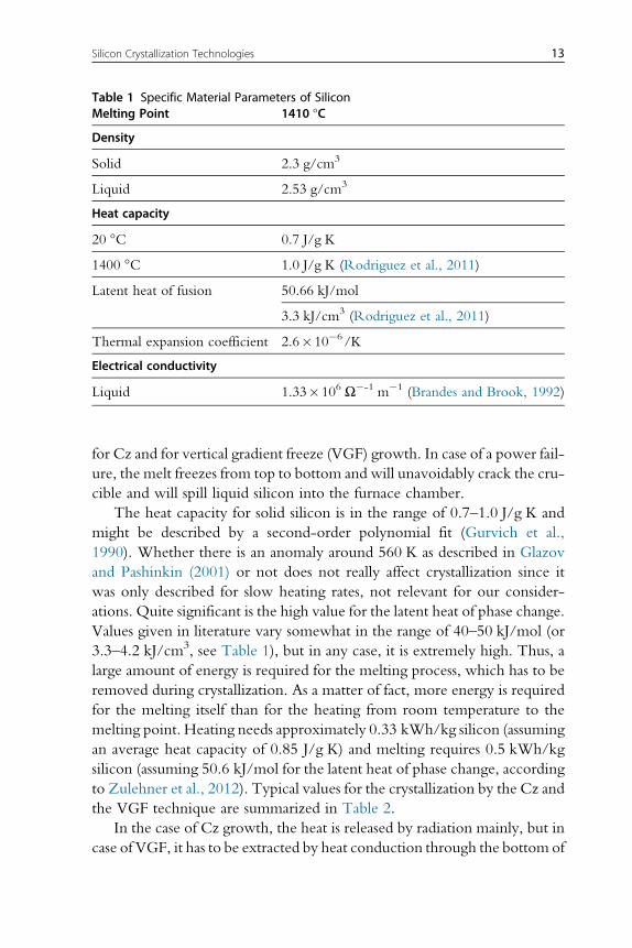
Table 1 Specific Material Parameters of SiliconMelting Point 1410 °C
Density
Solid 2.3 g/cm3
Liquid 2.53 g/cm3
Heat capacity
20 °C 0.7 J/g K
1400 °C 1.0 J/g K (Rodriguez et al., 2011)
Latent heat of fusion 50.66 kJ/mol
3.3 kJ/cm3 (Rodriguez et al., 2011)
Thermal expansion coefficient 2.6�10�6/K
Electrical conductivity
Liquid 1.33�106 Ω�-1 m�1 (Brandes and Brook, 1992)
13Silicon Crystallization Technologies
the crucible, where the crucible made of sintered quartz ceramic acts as an
insulation barrier.
Discussing the crystallization of silicon for PV application, it is helpful to
have a look at the actual size and geometry of the ingots (Table 3). Today,
standard wafer size is 156�156 mm2, either full square or pseudosquare in
case of certain mono ingots. Pseudosquare refers to the geometry with miss-
ing corners: to do without the four corners (the missing triangles have the
size of approximately 10�10�15 mm) reduces the active cell area by less
than 1% but allows to reduce the ingot diameter from 222 mm down to
206 mm (also referred to 900 vs. 800, even this is not exactly correct). Only
a few cell manufacturers are still using the 125�125 mm2 mono wafers.
It provides a higher utilization factor of the crystallized material but requires
more handling steps further down the manufacturing process chain in order
to get the same amount of active cell area. Quite likely, they will disappear
sooner or later from the market. In both cases, mono as well as multi, a sig-
nificant amount of crystallized material cannot be used as wafers. In the case
of mono, it is due to the fact that the ingot is cylindrical but the wafer is
rectangular; in the case of multi, it is due to the impurity-rich areas near
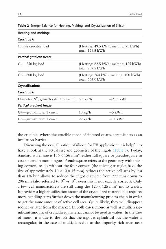
Table 2 Energy Balance for Heating, Melting, and Crystallization of Silicon
Heating and melting:
Czochralski
150 kg crucible load (Heating: 49.5 kWh; melting: 75 kWh)
total: 124.5 kWh
Vertical gradient freeze
G4—250 kg load (Heating: 82.5 kWh; melting: 125 kWh)
total: 207.5 kWh
G6—800 kg load (Heating: 264 kWh; melting: 400 kWh)
total: 664.0 kWh
Crystallization:
Czochralski
Diameter: 900; growth rate: 1 mm/min 5.5 kg/h �2.75 kWh
Vertical gradient freeze
G4—growth rate: 1 cm/h 10 kg/h �5 kWh
G6—growth rate: 1 cm/h 22 kg/h �11 kWh
14 Peter Dold
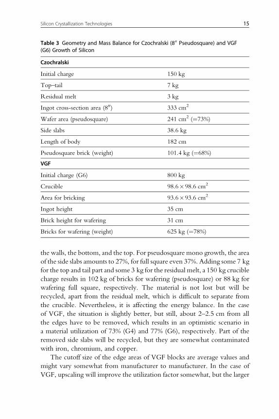
the walls, the bottom, and the top. For pseudosquare mono growth, the area
of the side slabs amounts to 27%, for full square even 37%. Adding some 7 kg
for the top and tail part and some 3 kg for the residual melt, a 150 kg crucible
charge results in 102 kg of bricks for wafering (pseudosquare) or 88 kg for
wafering full square, respectively. The material is not lost but will be
recycled, apart from the residual melt, which is difficult to separate from
the crucible. Nevertheless, it is affecting the energy balance. In the case
of VGF, the situation is slightly better, but still, about 2–2.5 cm from all
the edges have to be removed, which results in an optimistic scenario in
a material utilization of 73% (G4) and 77% (G6), respectively. Part of the
removed side slabs will be recycled, but they are somewhat contaminated
with iron, chromium, and copper.
The cutoff size of the edge areas of VGF blocks are average values and
might vary somewhat from manufacturer to manufacturer. In the case of
VGF, upscaling will improve the utilization factor somewhat, but the larger
Table 3 Geometry and Mass Balance for Czochralski (800 Pseudosquare) and VGF(G6) Growth of Silicon
Czochralski
Initial charge 150 kg
Top–tail 7 kg
Residual melt 3 kg
Ingot cross-section area (800) 333 cm2
Wafer area (pseudosquare) 241 cm2 (¼73%)
Side slabs 38.6 kg
Length of body 182 cm
Pseudosquare brick (weight) 101.4 kg (¼68%)
VGF
Initial charge (G6) 800 kg
Crucible 98.6�98.6 cm2
Area for bricking 93.6�93.6 cm2
Ingot height 35 cm
Brick height for wafering 31 cm
Bricks for wafering (weight) 625 kg (¼78%)
15Silicon Crystallization Technologies
melt volumes and the longer process times also increase the width of the sur-
face boundary layers with highmetal contamination and low carrier lifetimes
(“electrically dead zone”). The rather large loss of material was always a
strong motivation for direct wafer casting technologies (until the final wafers
are ready for the cell process, an additional 40–50% of the silicon from the
ready-to-cut bricks will get lost in the wire saw). However, as long as the
direct wafer technologies do not reach the same thickness as the wafers from
the multiwire process, which is in moment between 150 and 180 μm, there
is not a real advantage from the viewpoint of material utilization. In any case,
the rather lowmaterial utilization factor for crystalline silicon wafer technol-
ogy is a significant cost driver and it will be an important task for the future to
improve it.
An important material property of liquid silicon is its high chemical reac-
tivity. In contrast to solid silicon, which is protected by an oxide passivation
layer and thus is very easy to handle, liquid silicon is a highly aggressive sub-
stance. So far, no material is known, which is fully inert against silicon. Even
in the oxidized state as Si4+ (e.g., as SiO2, SiC, or Si3N4), there is always an
interaction with the melt and a certain dissolution or formation of precip-
itates can be observed. In particular, in the case of SiO2, the reaction will not
stop since the oxygen vapor pressure of SiO is rather high and it will evap-
orate at the free melt surface. Thus, the equilibrium always favors the further
dissolution of the quartz crucible. The dissolution rate for fused quartz
glass in contact with liquid silicon was reported to be in the range of
1.15�10�5 cm/min in the bulk of the melt and up to 8.4�10�5 cm/min
at the triple point melt–crucible–gas (Chaney and Varker, 1976).
A correlation with melt stirring was reported by Hirata and Hoshikawa
(1980) and a certain correlation to the boron concentration was found by
Abe et al. (1998), but the reported values were all in the same range. To
get a better idea of the amount of quartz glass dissolved during the course
of the growth run, we might assume a process time of 50 h and an average
crucible surface in contact to the melt of 2300 cm2 (for a 2400 crucible; at thebeginning, it will be around 5600 cm2 but decreases continuously). The cru-
cible wall would be reduced by about 0.35 mm on average, which correlates
to some 200–250 g of crucible material dissolved into the melt. The corro-
sion rate of the quartz glass crucible is a fundamental issue for multipulling or
for continuous Cz processes, and the development of high corrosion-
resistant crucible materials is essential. In the case of multicrystalline growth,
the crucible is protected by an Si3N4 coating, which cannot be used for Cz
growth, of course. Silicon nitride particles would result in structure loss.
16 Peter Dold
With regard to metals, we might distinguish four classes (Table 4): silicon
might form (A) solid solutions, (B) eutectics, and/or (C) intermetallic com-
ponents, or (D) shows a complete mixing in the liquid state, but as good as
no mixing in the solid. Quite often, eutectics and intermetallic components
are found in one phase diagram and sorting into the different classes is not
always a clear case. However, it helps to understand the interactions and
chemical reactions.
Some of the silicides have rather high melting points, e.g., MoSi2(Tm¼2020 °C) or TaSi2 (Tm¼2040 °C). However, the tolerable levels
of these metals for solar applications are extremely low, and concentrations
in the ppt range affect the cell efficiency already heavily (Coletti et al., n.d.;
Davis et al., 1980). Metals from class (D) are used for LPE and class (B) or
class (D) elements are candidates for the use in silicon refinement.
Whereas the high reactivity in the liquid state makes it difficult to find the
right crucible material, the low solubility in the solid helps quite significantly
for purification. Despite a few exceptions, most elements show small segre-
gation coefficients (the segregation coefficient k0 defines the ratio between
the concentration in the solid and the concentration in the liquid, under the
assumption of thermodynamic equilibrium) and will not be incorporated
into the crystal but will accumulate in the liquid boundary layer ahead of
the solid–liquid interface (Table 5). One exception is boron (k0¼0.8).
The large segregation coefficient of boron favors a uniform dopant distribu-
tion for p-type ingots—but it is quite troublesome for silicon purification.
A second exception is oxygen. With a segregation coefficient around 1, all
the oxygen near the solid–liquid interface will be incorporated into the crys-
tal. To prevent this, the transport of oxygen toward the interface has to be
reduced, which is possible by proper melt flow configurations. The oxygen-
rich melt should be moved away from the growing interface and should be
Table 4 Classification of Binary Silicon Phase Diagrams with Respect to the Formation ofSolid Solutions, Silicides, or Eutectics
(A) Solid solutions Ge
(B) Eutectics (low solubility in the solid) Al, Ag, Au, Bi, Pb
(C) Intermetallic compounds/silicides Cu, Ta, Fe, Mg, Mo,
Ni, Ti,
(D) Very limited solution in the solid, and complete
solubility in the liquid
Sn, In, Zn, Ga
17Silicon Crystallization Technologies
transported toward the free surface, where the oxygen (in form of SiO) can
evaporate and subsequently be removed from the growth chamber.
2.2 Numerical SimulationToday, numerical simulation is a standard tool for industrial crystallization.
In most cases, it is an integral part for any hardware or hot-zone develop-
ment. It helps to understand the heat fluxes (and losses), the material trans-
port, and reveals which areas are crucial for the optimization of the energy
consumption. The first attempts for computational simulation of crystalliza-
tion processes go back to the 1970s (e.g., Kobayashi, 1978). At that time, it
was still restricted to 2D axisymmetrical calculations based on finite differ-
ences and nonstructured grids. Now, modern software packages are running
on PC systems and are able to handle transient processes, 3D flows, and some
of them even chemical reactions. In particular, for the crystallization of sil-
icon, commercial codes are now tailored to specific growth technologies.
Examples for software packages dedicated to silicon crystal growth are,
e.g., CGSim (http://www.str-soft.com/products/CGSim/; Smirnov and
Kalaev, 2009), FEMAGSoft (https://www.femagsoft.com/; Collet et al.,
2012), or CrysVUn (Kurz et al., 1999; http://www.iisb.fraunhofer.de/
de/abteilungen/kristallzuechtung/crysmas.html) to mention just some of
them, or of course ANSYS (http://www.ansys.com/) as a more general
Table 5 Segregation Coefficient k0 for Various Elements in SiliconElement k0 Element k0 Element k0
Ag 1�10�6 Fe 8�10�6 O 1–1.25
Al 2�10�3 Ga 8�10�3 P 0.35
As 0.3 Ge 0.33 Pb 2�10�3
Au 2.5�10�3 In 4�10�4 S 10�5
B 0.8 Li 0.01 Sb 0.023
Ba <10�8 Mg 8�10�6 Se <10�8
Bi 7�10�4 Mn 10�5 Sn 0.016
C 7�10�2 Mo 4�10�8 Ta 10�7
Co 8�10�6 N 10�7 Te 8�10�6
Cr <10�8 Na 2�10�3
Cu 4�10�4 Ni 8�10�6
18 Peter Dold
software code for any kind of fluid dynamic problems. Quite often, the user
is enabled to add and integrate user-based subroutines, e.g., in order to sim-
ulate external magnetic fields. Therefore, numerical simulations became a
reliable and indispensable tool for any crystal grower. Nevertheless, certain
points have to be kept in mind when analyzing the results of numerical
simulations:
– In the simulation, the heat transfer is always idealized. In reality, it will be
reduced due to small gaps, surface layers, cracks, etc., or it might be
increased by altered material properties, enhanced emissivities, etc.
– Today, the material data are known much better than some 20 years ago.
Still, they are often idealized or not available as a function of the temper-
ature. Furthermore, they might change over time.
– Materials exposed to high temperatures and aggressive media will change
their structure and their surface. In particular, surface corrosion and sur-
face coatings have a huge impact on the temperature. Changes in the
emissivity affect the radiative heat transfer, which has a T4 impact on
the heat flux.
– The different length scales are difficult to handle. We have to deal with
macroscopic features in the meter range, but at the same time, chemical
reactions and surface-related phase changes have to be resolved in the
micrometer or even submicrometer range.
– Certain features have a 3D or a time-dependent characteristic. VGF is
nonaxisymmetric by definition. The large melt volumes result in large
Grashof and Reynolds numbers, indicating time-dependent 3D flow
structures.
– For certain aspects like defect formation, structure loss, or grain forma-
tion, the physics behind is not fully understood yet and the physical
models are not always adequate.
As long as these limitations are kept in mind, numerical simulations are an
extremely helpful tool. Most software programs became rather user-friendly
and the profile of a typical operator is shifting from a highly specialized sci-
entist toward an engineer with experimental background. But in any case,
the proper validation of numerical results by experimental data is absolutely
crucial.
3. CRYSTALLIZATION TECHNOLOGIES
In the following chapter, the main technologies for silicon crystalliza-
tion are described in detail: the Cz technique used for the majority of all
19Silicon Crystallization Technologies
mono ingots, the directional solidification or VGF method used for multi-
crystalline ingot production, and finally the FZ technique, a method well
established for the crystallization of electronic grade ingots, whenever low
oxygen material is required, but not yet adapted to the PV market. Also,
FZ would provide many benefits, and there are certain bottlenecks which
prevented the cost-competitive introduction of FZ wafers for solar cell
manufacturing until now. One serious problem is the availability of suitable
feedstock.
Other crystallization techniques for silicon could not gain a significant
market share so far. For example, the electromagnetic casting had made sig-
nificant progress; e.g., the Japanese company Sumco had shown impressive
pictures of 7 m tall ingots (“taller than a giraffe”—as they claimed in their
portfolio and their webpage; Kaneko, 2010; Kaneko et al., 2006;
SUMCOAnnual Report, 2008), but the technique was considered not cost
competitive and production was stopped. There had also been many activ-
ities with respect to sheet growth (EFG - Edge-defined Film Fed Growth by
Schott (Mackintosha et al., 2006), String Ribbon (van Glabbeek et al., 2008)
by Evergreen/Sovello, to mention just the most prominent ones), but so far,
none of them had really been able to reach the cost structure and/or the
quality of Cz and VGF.We will therefore focus in the following on the pre-
dominant and most promising PV silicon bulk crystallization technologies.
A detailed discussion of the different ribbon and foil techniques is provided
by Rodriguez et al. (2011).
3.1 Pulling from the Melt: The Cz TechniqueInitially, pulling a monocrystalline material from a melt goes back to
Czochralski (1918). Although the initial intention was not the growth of
large single crystals but the measurement of solidification velocities and
latent heat, it was soon realized that this method was perfectly suited for
the pulling of monocrystalline ingots. There is no direct interaction of
the growing crystal with the crucible material, and in situ observation of
the success (or failure) of the growth process is easily carried out. An excel-
lent overview about the historical development of silicon pulling from the
melt was given by Zulehner (1999); unfortunately, to the knowledge of the
author, it is only available as a conference proceeding paper.
3.1.1 Standard Cz GrowthSince more than half a century, the Cz technique is the workhorse for the
semiconductor industry. At the very beginning, there was a competition
20 Peter Dold
between FZ and Cz. The crucible-free growth and the lack of any graphite
or insulation material seemed to be in favor of the FZ method, but after the
development of proper quartz glass crucibles and hot zones based on purified
graphite, the easy scale-up option for Cz and the easier handling and oper-
ation of the crystallization process shifted the pendulum clearly toward Cz.
The point that for most semiconductor devices a certain oxygen concentra-
tion is beneficial for device manufacturing gave Cz additional credit and
soon the Cz technique had a market share for semiconductor ingots of more
than 90%. Exceptions are the low-in-oxygen wafers for power electronics,
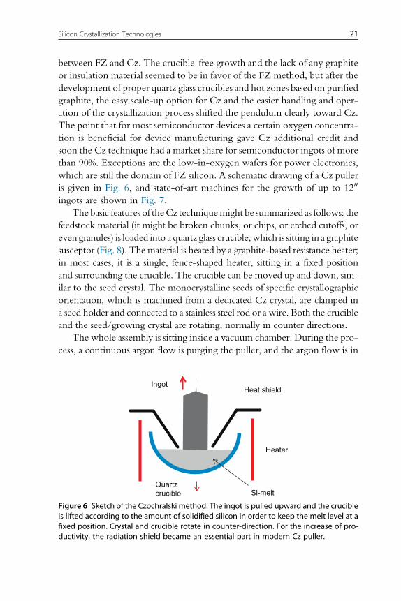
which are still the domain of FZ silicon. A schematic drawing of a Cz puller
is given in Fig. 6, and state-of-art machines for the growth of up to 1200
ingots are shown in Fig. 7.
The basic features of theCz techniquemight be summarized as follows: the
feedstock material (it might be broken chunks, or chips, or etched cutoffs, or
even granules) is loaded into a quartz glass crucible,which is sitting in a graphite
susceptor (Fig. 8). The material is heated by a graphite-based resistance heater;
in most cases, it is a single, fence-shaped heater, sitting in a fixed position
and surrounding the crucible. The crucible can be moved up and down, sim-
ilar to the seed crystal. The monocrystalline seeds of specific crystallographic
orientation, which is machined from a dedicated Cz crystal, are clamped in
a seed holder and connected to a stainless steel rod or a wire. Both the crucible
and the seed/growing crystal are rotating, normally in counter directions.
The whole assembly is sitting inside a vacuum chamber. During the pro-
cess, a continuous argon flow is purging the puller, and the argon flow is in
Heater
Heat shield
Quartzcrucible Si-melt
Ingot
Figure 6 Sketch of the Czochralski method: The ingot is pulled upward and the crucibleis lifted according to the amount of solidified silicon in order to keep the melt level at afixed position. Crystal and crucible rotate in counter-direction. For the increase of pro-ductivity, the radiation shield became an essential part in modern Cz puller.
21Silicon Crystallization Technologies
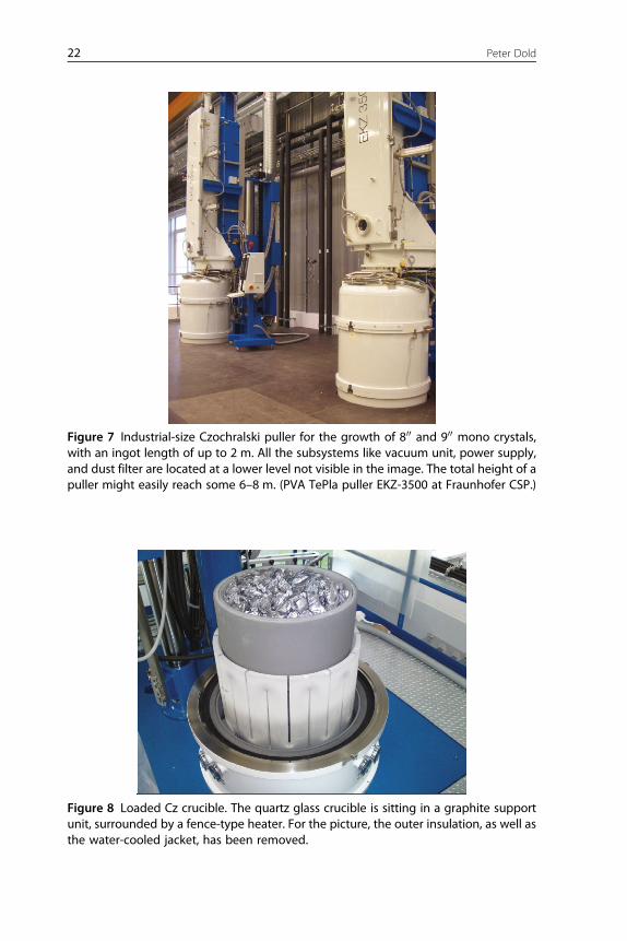
Figure 7 Industrial-size Czochralski puller for the growth of 800 and 900 mono crystals,with an ingot length of up to 2 m. All the subsystems like vacuum unit, power supply,and dust filter are located at a lower level not visible in the image. The total height of apuller might easily reach some 6–8 m. (PVA TePla puller EKZ-3500 at Fraunhofer CSP.)
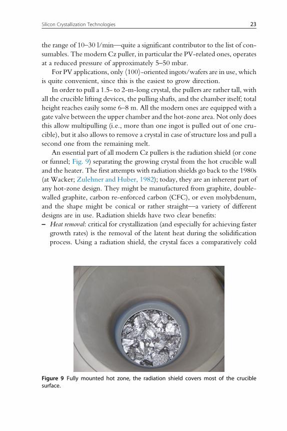
Figure 8 Loaded Cz crucible. The quartz glass crucible is sitting in a graphite supportunit, surrounded by a fence-type heater. For the picture, the outer insulation, as well asthe water-cooled jacket, has been removed.
22 Peter Dold
the range of 10–30 l/min—quite a significant contributor to the list of con-
sumables. The modern Cz puller, in particular the PV-related ones, operates
at a reduced pressure of approximately 5–50 mbar.
For PV applications, only h100i-oriented ingots/wafers are in use, whichis quite convenient, since this is the easiest to grow direction.
In order to pull a 1.5- to 2-m-long crystal, the pullers are rather tall, with
all the crucible lifting devices, the pulling shafts, and the chamber itself; total
height reaches easily some 6–8 m. All the modern ones are equipped with a
gate valve between the upper chamber and the hot-zone area. Not only does
this allow multipulling (i.e., more than one ingot is pulled out of one cru-
cible), but it also allows to remove a crystal in case of structure loss and pull a
second one from the remaining melt.
An essential part of all modern Cz pullers is the radiation shield (or cone
or funnel; Fig. 9) separating the growing crystal from the hot crucible wall
and the heater. The first attempts with radiation shields go back to the 1980s
(at Wacker; Zulehner and Huber, 1982); today, they are an inherent part of
any hot-zone design. They might be manufactured from graphite, double-
walled graphite, carbon re-enforced carbon (CFC), or even molybdenum,
and the shape might be conical or rather straight—a variety of different
designs are in use. Radiation shields have two clear benefits:
– Heat removal: critical for crystallization (and especially for achieving faster
growth rates) is the removal of the latent heat during the solidification
process. Using a radiation shield, the crystal faces a comparatively cold
Figure 9 Fully mounted hot zone, the radiation shield covers most of the cruciblesurface.
23Silicon Crystallization Technologies
surface. Without radiation shield, it would be exposed to the radiation
from the heater and the crucible.
– Guidance for the argon flow: in order to keep the oxygen concentration low,
the evaporating SiO from the melt surface has to be transported out of the
hot zone as fast as possible. The radiation shield guides the argon flow
along the crystal down to the melt surface, over the melt surface, upward
the crucible wall, and then downward to the bottom area where the pip-
ing for the exhaust system is located.
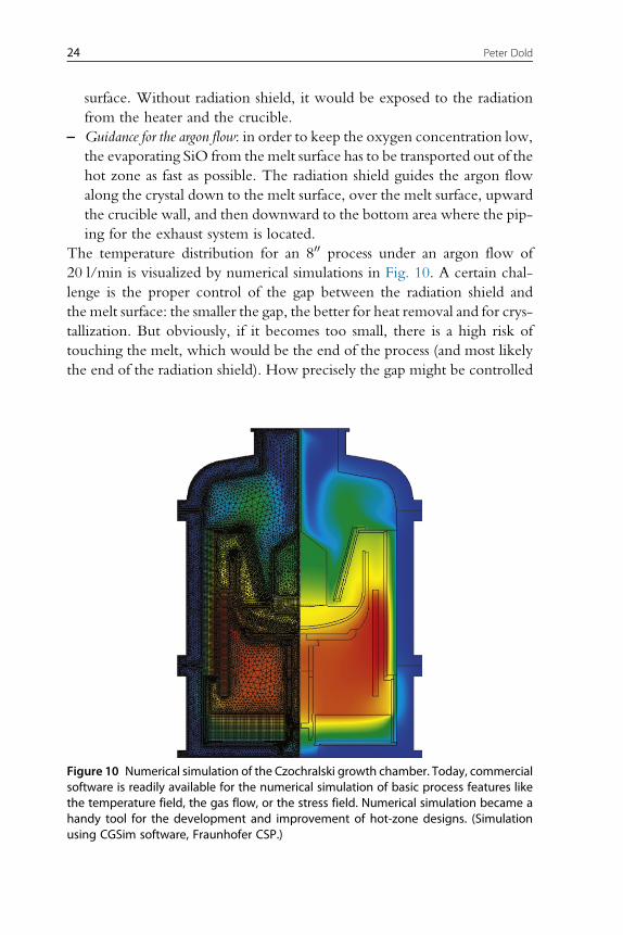
The temperature distribution for an 800 process under an argon flow of
20 l/min is visualized by numerical simulations in Fig. 10. A certain chal-
lenge is the proper control of the gap between the radiation shield and
the melt surface: the smaller the gap, the better for heat removal and for crys-
tallization. But obviously, if it becomes too small, there is a high risk of
touching the melt, which would be the end of the process (and most likely
the end of the radiation shield). How precisely the gap might be controlled
Figure 10 Numerical simulation of the Czochralski growth chamber. Today, commercialsoftware is readily available for the numerical simulation of basic process features likethe temperature field, the gas flow, or the stress field. Numerical simulation became ahandy tool for the development and improvement of hot-zone designs. (Simulationusing CGSim software, Fraunhofer CSP.)
24 Peter Dold
depends on the system used for growth control and for controlling the crystal
diameter. Since PV-crystal pullers are rather low-budget machines, quite
often, no fancy load cells or redundant measurements of weight and diam-
eter are used, but simple optical control of the diameter using CCD cameras.
Since the observation angle is rather steep with respect to the crystal axis
(there is no option for any optical access to the hot zone from the side or
any optical access through the crucible), accuracy is limited; e.g., an uncer-
tainty of half a millimeter on the crystal radius (for an 800 ingot) accumulates
over a crystal length of 200 cm to an incorrect calculation of the crystal
weight of approximately 1.5 kg and consequently a misinterpretation of
the position of the melt level.
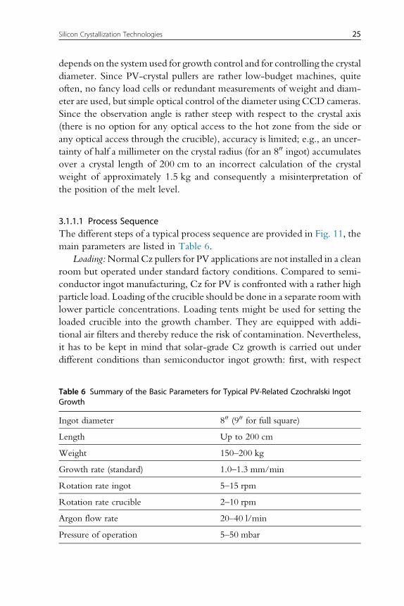
3.1.1.1 Process SequenceThe different steps of a typical process sequence are provided in Fig. 11, the
main parameters are listed in Table 6.
Loading:Normal Cz pullers for PV applications are not installed in a clean
room but operated under standard factory conditions. Compared to semi-
conductor ingot manufacturing, Cz for PV is confronted with a rather high
particle load. Loading of the crucible should be done in a separate roomwith
lower particle concentrations. Loading tents might be used for setting the
loaded crucible into the growth chamber. They are equipped with addi-
tional air filters and thereby reduce the risk of contamination. Nevertheless,
it has to be kept in mind that solar-grade Cz growth is carried out under
different conditions than semiconductor ingot growth: first, with respect
Table 6 Summary of the Basic Parameters for Typical PV-Related Czochralski IngotGrowth
Ingot diameter 800 (900 for full square)
Length Up to 200 cm
Weight 150–200 kg
Growth rate (standard) 1.0–1.3 mm/min
Rotation rate ingot 5–15 rpm
Rotation rate crucible 2–10 rpm
Argon flow rate 20–40 l/min
Pressure of operation 5–50 mbar
25Silicon Crystallization Technologies
to the material preparation (no chemical etching; after crushing, the
poly-feedstock goes straight into the crucible) and second, with respect to
the growth environment. It is obvious that higher defect densities are the
price for the envisaged cost savings.
Melting: The melting process is rather time consuming. It takes some
6–10 h, depending on the hot-zone design and the crucible charge. After
melting, melt homogenization, and temperature stabilization, the seed crys-
tal comes in contact with the melt.
Necking: Introduction of the necking process in 1958 by Dash (1958,
1959) was one of the great breakthroughs for silicon single-crystal growth.
To keep a growing crystal free of dislocations is relatively easy, in particular
in the case of silicon. As long as no major disturbances are imposed on the
growth conditions, the value for the critical resolved shear stress is large
enough to avoid the generation of dislocations. The challenge is, however,
to get a dislocation-free crystal. Even startingwith a dislocation-free seed, the
thermal shock, when the seed crystal comes in contact with themelt, induces
a high concentration of crystal defects. Silicon shows two distinct features:
first, the velocity with which dislocations can travel through the crystal is
comparatively low and only effective near the melting point. If the crystal
has reached some 1200 °C, they are more or less immobile. Second, silicon
can be crystallized with rather high growth rates, in particular for small diam-
eters when the amount of latent heat to be removed is still small. Since dis-
location in h100i silicon grows outwards, the crystal has simply to be pulled
faster than the dislocations can move or multiply along the growth axis.
Figure 11 The Czochralski process: top from left to right: the loaded crucible—meltingof the material—necking. Bottom from left to right: shoulder growth—shortly after thetransition to the body—body growth.
26 Peter Dold
Impressive pictures of the dislocation elimination are provided by Shimura
(2007). For the necking during Cz silicon, typical parameters are as follows:
– Pulling rate: >5 mm/min
– Diameter: <4 mm, preferably <3.5 mm, or even more preferably
<3 mm
– Length of neck: >50 mm
These values are guidelines to the best knowledge of the author. No exact
threshold values have beenmeasured or published so far and everyone has his
own set of parameters. And once it works, it will not be changed anymore.
For all the substances crystallized on an industrial scale, necking works best
for silicon. It is also applicable to other single elements (e.g., germanium or
metals) but fails for binary substances (e.g., GaAs or CdTe). In binary or
multinary crystals, dislocations travel too fast and the corresponding growth
rates are too small.
Shoulder: After necking, the growth velocity is reduced and the melt
temperature is lowered in order to achieve an increase in the diameter.
The shoulder length for an 800 ingot is typically in the range of approximately
50–100 mm.
Body: The growth continues with constant diameter (and minimal var-
iations of the crystal diameter), 800 for pseudosquare and 900 for full square.Standard growth rates are around 1 mm/min. With sophisticated hot-zone
designs, some 1.3 mm/min is possible. Trends and new developments try to
further increase it; a promising approach is the integration of an active
cooling ring. A 2-m-long ingot might be crystallized within 25–35 h,
depending on the system. But the whole cycle time amounts to 50–60 h,
which explains the recent developments toward multipulling, continuous
pulling, and so on.
Cone: A slow reduction of the ingot diameter at the end of the run is
essential to avoid thermal shock, which would immediately induce disloca-
tions and slip planes. Since they are preferentially arranged in 45° angles,they might move back some 200–250 mm. If the diameter of the crystal
is controlled by a CCD camera only, the end cone is not visible and this part
has to be crystallized on preset parameters. If a load cell is used, the cone is
controlled actively.
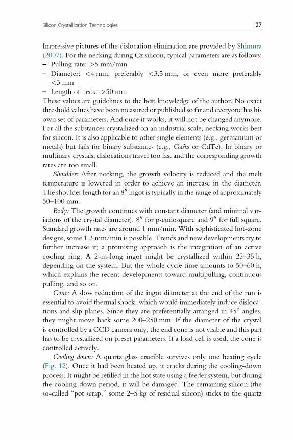
Cooling down: A quartz glass crucible survives only one heating cycle
(Fig. 12). Once it had been heated up, it cracks during the cooling-down
process. It might be refilled in the hot state using a feeder system, but during
the cooling-down period, it will be damaged. The remaining silicon (the
so-called “pot scrap,” some 2–5 kg of residual silicon) sticks to the quartz
27Silicon Crystallization Technologies
glass crucible, and due to the different thermal expansion coefficients, the
quartz glass brakes. In addition, a phase change of the quartz glass into
cristobalite starts during the crystallization process, and these two substances
have different thermal expansion coefficients. Since the modern machines
are rather well insulated, the cooling down from over 1500 °C to temper-
atures low enough for cleaning and crucible replacement takes several hours,
a downtime of the puller which is unproductive of course.
3.1.1.2 The Main Cost DriversCrucibles: As explained above, crucibles are for single use only. Under this
consideration, it would be attractive to use crucibles as cheap as possible.
On the other hand, a cruciblewhich does not survive thewhole growth cycle
might destroy the entire hot zone. Furthermore, crucibles are dissolvedwhile
they are in contact with liquid silicon. Metallic impurities from the quartz
glass will accumulate in the melt and finally will be incorporated in the ingot.
In particular, Fe has to be mentioned, but Al, Ca Cr, Fe, Mn, Na, or K are
typical impurities, too. In order to increase the lifetime of the crucible, which
is a crucial topic for all developments toward multipulling or continuous
growth, multilayer designs are in use and/or doping the inner layer with bar-
ium is another promising innovation (Wakita et al., 2013).
Figure 12 Pot scrap: 2–5 kg of residual melt remains in the crucible and sticks to thequartz glass. The crucible cracks during the cooling-down process and has to be dis-posed. Recycling of the pot scrap is difficult; the separation of the silicon from the quartzrequires mechanical and chemical process steps. Further, impurities are accumulated inthe pot scrap.
28 Peter Dold

Hot zone: The graphite parts are consumables, too, and their life span is
normally in the range of 10 tomaybe 50 cycles, depending on their work and
heat load. Since a full hot zone might easily cost some 20,000–40,000 US$depending on the graphite purity and manufacturing costs, the hot zone
contributes quite significantly to the operating cost. Multipulling might help
to increase the lifetime of graphite parts, because they will see less heating
cycles, but at the end, there is not really a lot which can be done to lower
the cost without affecting the purity and the quality of the final product.
Coated graphite parts (e.g., SiC-coated) or CFC-enforced graphite felt is
beneficial for the purity and the life span of the corresponding part, but it
is significantly more expensive than the standard materials.
Argon:During the whole growth cycle, a continuous argon flow is essen-
tial in order to remove the SiO. Quartz glass is permanently dissolved by
liquid silicon. Fortunately, more than 99% of the oxygen evaporates as
SiO, which condensates at cooler surfaces. The argon flow helps to transport
most of the SiO to the outside of the growth chamber, where it might be
oxidized in a controlled manner after the growth.5 Further, the continuous
removal of SiO from the melt surface keeps the equilibrium on the silicon-
rich side and supports the evaporation of the SiO. Argon recovery systems
are available and they might be an option to reduce the Operational Expen-
ditures (OPEX).
Process time/productivity: A scale-up as we see it for directional solidifica-
tion, going from G4 to G5 to G6 and so on, is not possible for Cz growth.
Increasing the diameter in such a way that four bricks are cut out of the
grown ingot instead of one brick would require a crystal diameter of
445 mm, which is not cost effective. In addition to the higher OPEX
and CAPEX, the growth rate for such large ingots is reduced compared
to the one of an 800 standard ingot, since the removal of the latent heat is
more difficult. Thus, an increase of the productivity has to be coupled with
an increase of the growth rate and/or a reduction of the downtime.
Yield/structure loss: Structure loss is an important (or maybe the most
important) parameter for the calculation of the real cost of ownership and
the final dollar per wafer price. One of the great features of the Cz method
is the fact that a loss of single crystallinity is detected immediately or it is even
anticipated by careful observation of the structure and pronunciation of the
four growth lines. Figure 13 shows the growth facets during the crystalliza-
tion of the shoulder. If the facets are not all equally well pronounced or if one
5 As a fine powder, SiO is a pyrophoric substance, which has to be handled with great care.
29Silicon Crystallization Technologies
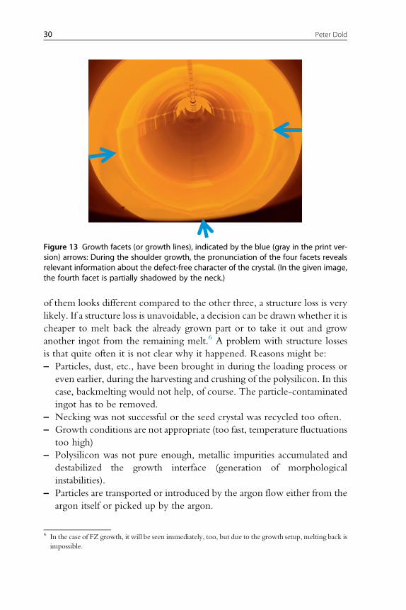
of them looks different compared to the other three, a structure loss is very
likely. If a structure loss is unavoidable, a decision can be drawn whether it is
cheaper to melt back the already grown part or to take it out and grow
another ingot from the remaining melt.6 A problem with structure losses
is that quite often it is not clear why it happened. Reasons might be:
– Particles, dust, etc., have been brought in during the loading process or
even earlier, during the harvesting and crushing of the polysilicon. In this
case, backmelting would not help, of course. The particle-contaminated
ingot has to be removed.
– Necking was not successful or the seed crystal was recycled too often.
– Growth conditions are not appropriate (too fast, temperature fluctuations
too high)
– Polysilicon was not pure enough, metallic impurities accumulated and
destabilized the growth interface (generation of morphological
instabilities).
– Particles are transported or introduced by the argon flow either from the
argon itself or picked up by the argon.
Figure 13 Growth facets (or growth lines), indicated by the blue (gray in the print ver-sion) arrows: During the shoulder growth, the pronunciation of the four facets revealsrelevant information about the defect-free character of the crystal. (In the given image,the fourth facet is partially shadowed by the neck.)
6 In the case of FZ growth, it will be seen immediately, too, but due to the growth setup, melting back is
impossible.
30 Peter Dold
– Crucible corrosion results in a flaking off of quartz glass which might stick
to the growth interface.
For sure, there are many other reasons not listed here, but it becomes clear
that the growth of single crystals by the Cz method does not allow many
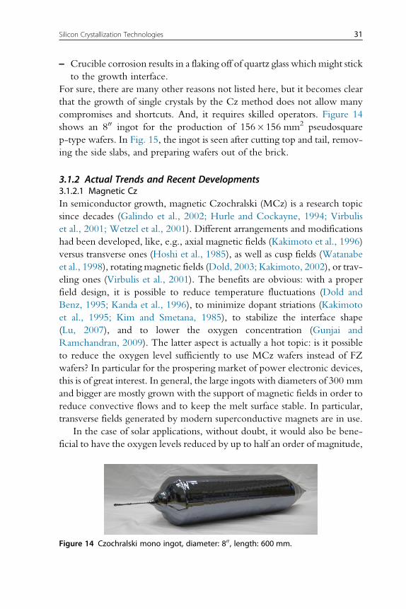
compromises and shortcuts. And, it requires skilled operators. Figure 14
shows an 800 ingot for the production of 156�156 mm2 pseudosquare
p-type wafers. In Fig. 15, the ingot is seen after cutting top and tail, remov-
ing the side slabs, and preparing wafers out of the brick.
3.1.2 Actual Trends and Recent Developments3.1.2.1 Magnetic CzIn semiconductor growth, magnetic Czochralski (MCz) is a research topic
since decades (Galindo et al., 2002; Hurle and Cockayne, 1994; Virbulis
et al., 2001; Wetzel et al., 2001). Different arrangements and modifications
had been developed, like, e.g., axial magnetic fields (Kakimoto et al., 1996)
versus transverse ones (Hoshi et al., 1985), as well as cusp fields (Watanabe
et al., 1998), rotating magnetic fields (Dold, 2003; Kakimoto, 2002), or trav-
eling ones (Virbulis et al., 2001). The benefits are obvious: with a proper
field design, it is possible to reduce temperature fluctuations (Dold and
Benz, 1995; Kanda et al., 1996), to minimize dopant striations (Kakimoto
et al., 1995; Kim and Smetana, 1985), to stabilize the interface shape
(Lu, 2007), and to lower the oxygen concentration (Gunjai and
Ramchandran, 2009). The latter aspect is actually a hot topic: is it possible
to reduce the oxygen level sufficiently to use MCz wafers instead of FZ
wafers? In particular for the prospering market of power electronic devices,
this is of great interest. In general, the large ingots with diameters of 300 mm
and bigger are mostly grown with the support of magnetic fields in order to
reduce convective flows and to keep the melt surface stable. In particular,
transverse fields generated by modern superconductive magnets are in use.
In the case of solar applications, without doubt, it would also be bene-
ficial to have the oxygen levels reduced by up to half an order of magnitude,
Figure 14 Czochralski mono ingot, diameter: 800, length: 600 mm.
31Silicon Crystallization Technologies

especially for boron-doped wafers in order to counteract LID (light-induced
degradation due to formation of boron–oxygen complexes). On the other
hand, the installation of a magnet increases the equipment costs substantially.
With the small margin ingot manufacturers are confronted with at the
moment, magnetic fields are not really an option. The improvement in qual-
ity is not justifying the cost.
3.1.2.2 Active CoolingAs pointed out earlier, the main limitation for the growth rate in Cz
silicon growth is the removal of the latent heat. We will see later that,
e.g., FZ ingots might be pulled twice as fast as Cz counterparts, simply
because of the higher heat flow. The first major breakthrough was the
insert of radiation shields in the 1980s. Recently, in order to enhance the
heat removal evenmore, active crystal cooling systems have been developed:
the growing crystal is surrounded by a water-cooled ring or a water-cooled
Figure 15 After the growth process, the ingot is squared and wafered. The side slabs,the top, and the tail are recycled.
32 Peter Dold
spiral (http://www.pvatepla.com/en/products/crystal-growing-systems/
pva/cz—equipment/active-crystal-cooling). The axial position is some
20–50 cm above the solid–liquid interface. Since the optical access to the
meniscus area is mandatory for diameter control, there is a limited degree
of freedomwith respect to positioning of the water-cooling system. Accord-
ing to the manufacturer, the active cooling might increase the pulling veloc-
ity by 20–40%.Obviously, inserting a water-cooled system into the hot zone
and in particular within the proximity of liquid silicon bears a certain risk.
Since it has to be machined from metal, any contact between the water-
cooled device and the growing crystal has to be avoided. Anyway, it is an
interesting approach and it will increase the productivity and thus will fur-
ther reduce cost. Furthermore, it shows that even for the rather matured Cz
pullers, there is still room for improvements.
3.1.2.3 Multipulling, Feeding, and Continuous GrowthThe Cz process is a batch process with high consumable costs. Therefore,
since the early days of Cz growth, there had been many ideas and many pat-
ents to overcome these weaknesses by developing a semicontinuous or a
continuous process (Altekruger, 1994; Lorenzini et al., 1977; Wang et al.,
2003; Zulehner, 1982). The biggest problems when operating a continuous
system are the reactivity of liquid silicon, the zero tolerance of the process for
particles, and the increase of complexity of the whole system. For the pro-
duction of electronic grade material for the semiconductor industry, the
technical problems never had been solved satisfyingly. With solar-grade sil-
icon, the situation is now different. Compared to the semiconductor mate-
rial, the ingot specifications are somewhat more relaxed: whereas the
semiconductor industry tries to minimize the concentrations of vacancies
and interstitials and, in any case, dislocations are a complete no-go criteria
for solar applications, an ingot with a certain defect structure or even with
an etch pit density of 103 cm�2 is still acceptable. Nevertheless, even with
the development of new materials, better crucibles, and more advanced
pullers, certain bottlenecks are still present:
– The crucible life span is a limiting factor.
– “Feedable” material of high purity is required.
– Accumulation of impurities in the melt has to be avoided and only high-
quality feedstock should be used.
The benefits of solving these problems are obvious: downtime is reduced,
which increases the productivity, and in addition, cost for consumables is
lowered. Actually, there are two different approaches: (I) batch feeding
and (II) continuous feeding. Figure 16 shows a feeder system for batch
33Silicon Crystallization Technologies
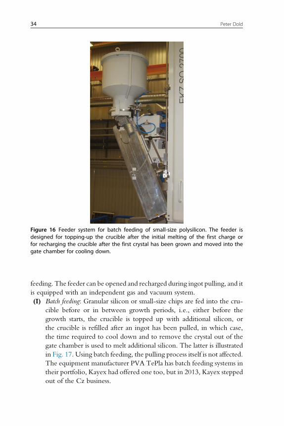
feeding. The feeder can be opened and recharged during ingot pulling, and it
is equipped with an independent gas and vacuum system.
(I) Batch feeding: Granular silicon or small-size chips are fed into the cru-
cible before or in between growth periods, i.e., either before the
growth starts, the crucible is topped up with additional silicon, or
the crucible is refilled after an ingot has been pulled, in which case,
the time required to cool down and to remove the crystal out of the
gate chamber is used to melt additional silicon. The latter is illustrated
in Fig. 17. Using batch feeding, the pulling process itself is not affected.
The equipment manufacturer PVA TePla has batch feeding systems in
their portfolio, Kayex had offered one too, but in 2013, Kayex stepped
out of the Cz business.
Figure 16 Feeder system for batch feeding of small-size polysilicon. The feeder isdesigned for topping-up the crucible after the initial melting of the first charge orfor recharging the crucible after the first crystal has been grown and moved into thegate chamber for cooling down.
34 Peter Dold
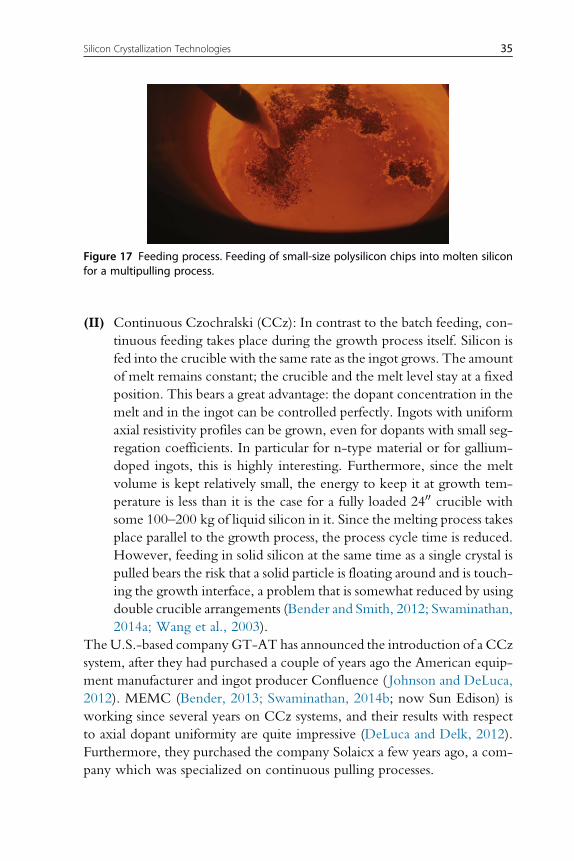
(II) Continuous Czochralski (CCz): In contrast to the batch feeding, con-
tinuous feeding takes place during the growth process itself. Silicon is
fed into the crucible with the same rate as the ingot grows. The amount
of melt remains constant; the crucible and the melt level stay at a fixed
position. This bears a great advantage: the dopant concentration in the
melt and in the ingot can be controlled perfectly. Ingots with uniform
axial resistivity profiles can be grown, even for dopants with small seg-
regation coefficients. In particular for n-type material or for gallium-
doped ingots, this is highly interesting. Furthermore, since the melt
volume is kept relatively small, the energy to keep it at growth tem-
perature is less than it is the case for a fully loaded 2400 crucible with
some 100–200 kg of liquid silicon in it. Since the melting process takes
place parallel to the growth process, the process cycle time is reduced.
However, feeding in solid silicon at the same time as a single crystal is
pulled bears the risk that a solid particle is floating around and is touch-
ing the growth interface, a problem that is somewhat reduced by using
double crucible arrangements (Bender and Smith, 2012; Swaminathan,
2014a; Wang et al., 2003).
TheU.S.-based company GT-AT has announced the introduction of a CCz
system, after they had purchased a couple of years ago the American equip-
ment manufacturer and ingot producer Confluence ( Johnson and DeLuca,
2012). MEMC (Bender, 2013; Swaminathan, 2014b; now Sun Edison) is
working since several years on CCz systems, and their results with respect
to axial dopant uniformity are quite impressive (DeLuca and Delk, 2012).
Furthermore, they purchased the company Solaicx a few years ago, a com-
pany which was specialized on continuous pulling processes.
Figure 17 Feeding process. Feeding of small-size polysilicon chips into molten siliconfor a multipulling process.
35Silicon Crystallization Technologies
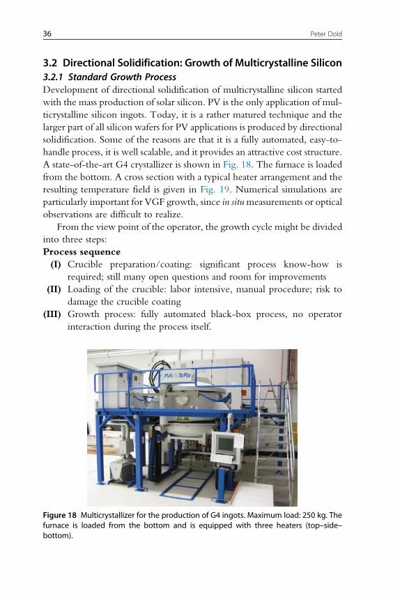
3.2 Directional Solidification: Growth of Multicrystalline Silicon3.2.1 Standard Growth ProcessDevelopment of directional solidification of multicrystalline silicon started
with the mass production of solar silicon. PV is the only application of mul-
ticrystalline silicon ingots. Today, it is a rather matured technique and the
larger part of all silicon wafers for PV applications is produced by directional
solidification. Some of the reasons are that it is a fully automated, easy-to-
handle process, it is well scalable, and it provides an attractive cost structure.
A state-of-the-art G4 crystallizer is shown in Fig. 18. The furnace is loaded
from the bottom. A cross section with a typical heater arrangement and the
resulting temperature field is given in Fig. 19. Numerical simulations are
particularly important for VGF growth, since in situmeasurements or optical
observations are difficult to realize.
From the view point of the operator, the growth cycle might be divided
into three steps:
Process sequence
(I) Crucible preparation/coating: significant process know-how is
required; still many open questions and room for improvements
(II) Loading of the crucible: labor intensive, manual procedure; risk to
damage the crucible coating
(III) Growth process: fully automated black-box process, no operator
interaction during the process itself.
Figure 18 Multicrystallizer for the production of G4 ingots. Maximum load: 250 kg. Thefurnace is loaded from the bottom and is equipped with three heaters (top–side–bottom).
36 Peter Dold
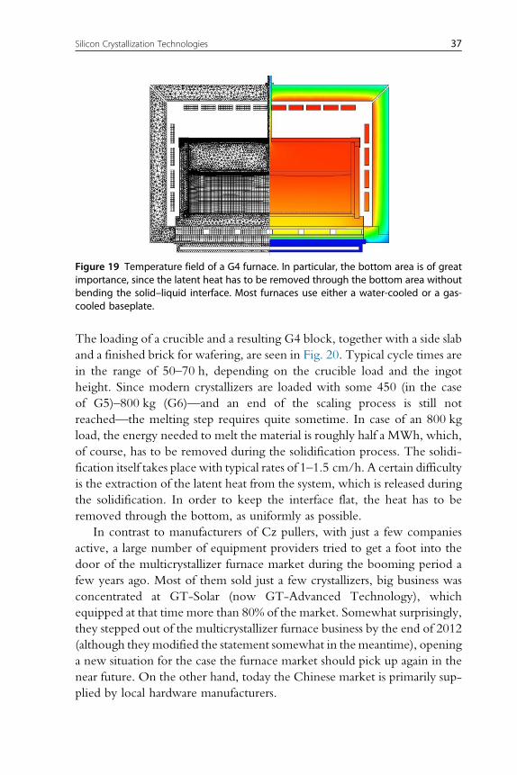
The loading of a crucible and a resulting G4 block, together with a side slab
and a finished brick for wafering, are seen in Fig. 20. Typical cycle times are
in the range of 50–70 h, depending on the crucible load and the ingot
height. Since modern crystallizers are loaded with some 450 (in the case
of G5)–800 kg (G6)—and an end of the scaling process is still not
reached—the melting step requires quite sometime. In case of an 800 kg
load, the energy needed to melt the material is roughly half a MWh, which,
of course, has to be removed during the solidification process. The solidi-
fication itself takes place with typical rates of 1–1.5 cm/h. A certain difficulty
is the extraction of the latent heat from the system, which is released during
the solidification. In order to keep the interface flat, the heat has to be
removed through the bottom, as uniformly as possible.
In contrast to manufacturers of Cz pullers, with just a few companies
active, a large number of equipment providers tried to get a foot into the
door of the multicrystallizer furnace market during the booming period a
few years ago. Most of them sold just a few crystallizers, big business was
concentrated at GT-Solar (now GT-Advanced Technology), which
equipped at that time more than 80% of the market. Somewhat surprisingly,
they stepped out of the multicrystallizer furnace business by the end of 2012
(although they modified the statement somewhat in the meantime), opening
a new situation for the case the furnace market should pick up again in the
near future. On the other hand, today the Chinese market is primarily sup-
plied by local hardware manufacturers.
Figure 19 Temperature field of a G4 furnace. In particular, the bottom area is of greatimportance, since the latent heat has to be removed through the bottom area withoutbending the solid–liquid interface. Most furnaces use either a water-cooled or a gas-cooled baseplate.
37Silicon Crystallization Technologies
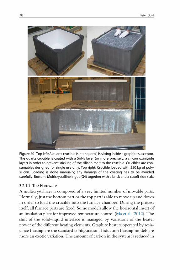
3.2.1.1 The HardwareA multicrystallizer is composed of a very limited number of movable parts.
Normally, just the bottom part or the top part is able to move up and down
in order to load the crucible into the furnace chamber. During the process
itself, all furnace parts are fixed. Some models allow the horizontal insert of
an insulation plate for improved temperature control (Ma et al., 2012). The
shift of the solid–liquid interface is managed by variations of the heater
power of the different heating elements. Graphite heaters operated by resis-
tance heating are the standard configuration. Induction heating models are
more an exotic variation. The amount of carbon in the system is reduced in
Figure 20 Top left: A quartz crucible (sinter quartz) is sitting inside a graphite susceptor.The quartz crucible is coated with a Si3N4 layer (or more precisely, a silicon oxinitridelayer) in order to prevent sticking of the silicon melt to the crucible. Crucibles are con-sumables designed for single use only. Top right: Crucible loaded with 250 kg of poly-silicon. Loading is done manually; any damage of the coating has to be avoidedcarefully. Bottom: Multicrystalline ingot (G4) together with a brick and a cutoff side slab.
38 Peter Dold
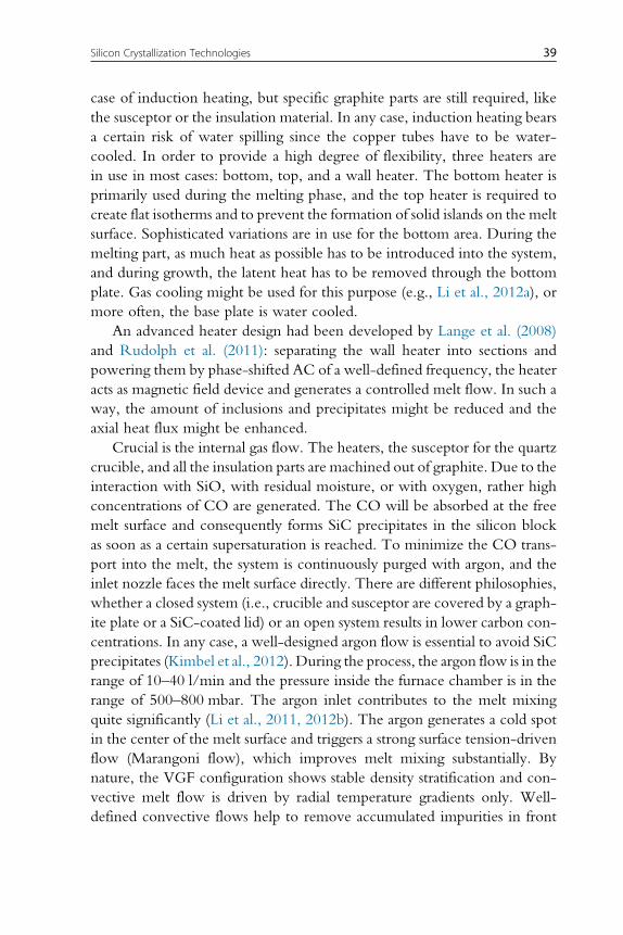
case of induction heating, but specific graphite parts are still required, like
the susceptor or the insulation material. In any case, induction heating bears
a certain risk of water spilling since the copper tubes have to be water-
cooled. In order to provide a high degree of flexibility, three heaters are
in use in most cases: bottom, top, and a wall heater. The bottom heater is
primarily used during the melting phase, and the top heater is required to
create flat isotherms and to prevent the formation of solid islands on the melt
surface. Sophisticated variations are in use for the bottom area. During the
melting part, as much heat as possible has to be introduced into the system,
and during growth, the latent heat has to be removed through the bottom
plate. Gas cooling might be used for this purpose (e.g., Li et al., 2012a), or
more often, the base plate is water cooled.
An advanced heater design had been developed by Lange et al. (2008)
and Rudolph et al. (2011): separating the wall heater into sections and
powering them by phase-shifted AC of a well-defined frequency, the heater
acts as magnetic field device and generates a controlled melt flow. In such a
way, the amount of inclusions and precipitates might be reduced and the
axial heat flux might be enhanced.
Crucial is the internal gas flow. The heaters, the susceptor for the quartz
crucible, and all the insulation parts are machined out of graphite. Due to the
interaction with SiO, with residual moisture, or with oxygen, rather high
concentrations of CO are generated. The CO will be absorbed at the free
melt surface and consequently forms SiC precipitates in the silicon block
as soon as a certain supersaturation is reached. To minimize the CO trans-
port into the melt, the system is continuously purged with argon, and the
inlet nozzle faces the melt surface directly. There are different philosophies,
whether a closed system (i.e., crucible and susceptor are covered by a graph-
ite plate or a SiC-coated lid) or an open system results in lower carbon con-
centrations. In any case, a well-designed argon flow is essential to avoid SiC
precipitates (Kimbel et al., 2012). During the process, the argon flow is in the
range of 10–40 l/min and the pressure inside the furnace chamber is in the
range of 500–800 mbar. The argon inlet contributes to the melt mixing
quite significantly (Li et al., 2011, 2012b). The argon generates a cold spot
in the center of the melt surface and triggers a strong surface tension-driven
flow (Marangoni flow), which improves melt mixing substantially. By
nature, the VGF configuration shows stable density stratification and con-
vective melt flow is driven by radial temperature gradients only. Well-
defined convective flows help to remove accumulated impurities in front
39Silicon Crystallization Technologies
of the growing interface and they enhance the heat transport. In conclusion,
a well-designed argon flow stabilizes the growth process.
3.2.1.2 Growth ProcessA multicrystallizer furnace is a black box with a minimum of interaction
from the operator. Once the process is started, it follows the preprogrammed
recipe: (I) heating up, melting, and melt homogenization; (II) nucleation
and growth by reducing the heater power of the bottom and the wall heater;
and (III) the cooling-down phase, bringing the whole block to a uniform
temperature and cooling it down without introducing thermal stress. As
pointed out already, the growth process follows a predefined program,
because optical access is very limited. There are not a lot of options to find
the proper parameters, like position of the interface as a function of the
heater power. Awidespreadmethod is the use of graphite rods or quartz glass
rods which are lowered downward through the melt until they touch the
solid–liquid interface (Trempa et al., 2010). This step is then repeated for
several sets of parameters, and based on the position of the solid–liquid inter-
face, the growth rate is calculated and the recipe is modified. There is a cer-
tain risk that the rod breaks. But in any case, the silicon block is
contaminated by carbon. Another option is the measurement of the melt
level by laser systems (Dold et al., 2014a; Muller et al., 2004): During solid-
ification, silicon expands by about 10%; i.e., during the course of the solid-
ification process, a melt of 25 cm in height will move upward by about
2.5 cm (see Fig. 21). The information is integral and the shape of the
solid–liquid interface is not accessible. The great advantage is the contactless
in situ measurement, where the growth process is not disturbed at all and it
might be used for the optimization of the recipe or for process control during
the production process.
3.2.1.3 Crucible CoatingIn contrast to the fused quartz glass crucibles as used for Cz growth, crucibles
for VGF are made out of sintered quartz ceramics. This is attributed to the
size, the rectangular shape, and the cost structure. Between the crucible and
the silicon, a coating layer is essential. Otherwise, the silicon would react
with the quartz and would stick to it, which would result in cracking of
the crucible and spilling of the melt. The coating consists mainly of Si3N4
particles and some binder, which are applied by spraying as a water-based
solution onto the crucible inner surfaces and the crucible is subsequently
40 Peter Dold
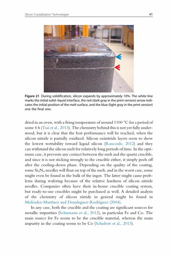
dried in an oven, with a firing temperature of around 1100 °C for a period of
some 4 h (Tsai et al., 2013). The chemistry behind this is not yet fully under-
stood, but it is clear that the best performance will be reached, when the
silicon nitride is partially oxidized. Silicon oxinitride layers seem to show
the lowest wettability toward liquid silicon (Rancoule, 2012) and they
can withstand the silicon melt for relatively long periods of time. In the opti-
mum case, it prevents any contact between the melt and the quartz crucible,
and since it is not sticking strongly to the crucible either, it simply peels off
after the cooling-down phase. Depending on the quality of the coating,
some Si3N4 needles will float on top of the melt, and in the worst case, some
might even be found in the bulk of the ingot. The latter might cause prob-
lems during wafering because of the relative hardness of silicon nitride
needles. Companies often have their in-house crucible coating system,
but ready-to-use crucibles might be purchased as well. A detailed analysis
of the chemistry of silicon nitride in general might be found in
Melendez-Martınez and Domınguez-Rodrıguez (2004).
In any case, both the crucible and the coating are significant sources for
metallic impurities (Schumann et al., 2012), in particular Fe and Co. The
main source for Fe seems to be the crucible material, whereas the main
impurity in the coating seems to be Co (Schubert et al., 2013).
Figure 21 During solidification, silicon expands by approximately 10%. The white linemarks the initial solid–liquid interface, the red (dark gray in the print version) arrow indi-cates the initial position of the melt surface, and the blue (light gray in the print version)one the final one.
41Silicon Crystallization Technologies
3.2.2 Actual Trends3.2.2.1 ScalingScaling is not really an actual trend but more an ongoing development.
Some companies still use G4 but this is rather the exception. The letter
G refers to “Generation” and the number to the number of bricks in a line,
i.e., G4, would be a block from which 4�4¼16 bricks are cut out, G5
would be 25 bricks, and so on. G5 is widely used, but newly installed fur-
naces are often in the G6 or even G7 range. For a G7 process with a silicon
charge of 1200 kg, a process cycle time of 90 h was reported recently by
Konca Solar Cell during the European PVSEC conference (Wang, 2014).
The challenge is to bring in the heat without overheating the edge areas
and, of course, to extract the heat uniformly through the bottom part.
Another development is the increase of the brick height. We have seen ear-
lier that VGF ingots are rather flat. A typical G4 block is some 22–24 cm tall,
and the G6 height is in the range of 35 cm. Limitations for taller ingots are
the manufacturing of the crucibles itself and the increasing distance of the
top heater to the melt surface with increasing ingot height. The relatively
low fill factor of the crucible with polysilicon requires a crucible about a fac-
tor of 2 taller than the final ingot will be. After melting, there will be a sig-
nificant gap between the top heater and the melt surface. To overcome the
limitations of the crucible manufacturing, the company Schott had added an
additional ring of quartz ceramic on top of a standard crucible, which
allowed them to charge more silicon into the system and grow taller ingots
from standard crucibles. Another option is the feeding of additional silicon
into the furnace once the initial charge is molten. For large systems, several
hundred kilograms of silicon have to be fed into the melt, which is quite a
challenge. It has to be kept in mind that the crucible will then stay longer in
the hot state and will be longer in contact with the liquid silicon which
increases the impurity concentration and requires a better coating.
Scaling seems not to have reached the end yet, since it is relatively simple
to realize and the cost-saving potential is quite obvious.
3.2.2.2 Mono-Like GrowthMono-like (or quasi-mono or mono-casting) was first introduced by
Stoddard et al. from BP Solar in 2006 (http://www.bp.com/en/global/
corporate/press/press-releases/bp-solar-introduces-mono.html; Stoddard
et al., 2008), and very soon, they presented some excellent in-depth inves-
tigations on this new approach. In the following years, it was rather quiet
about mono-like growth, until 2011/2012, when a huge hype started and
42 Peter Dold
all the major ingot manufacturers came up with mono-like ingots, and con-
sequently, modules based on mono-like wafers. In 2012, the ITRPV report
(www.itrpv.net/Reports/Downloads/2012) forecasted that by 2020,
mono-like will be the predominant growth technology with a total market
share of all crystalline silicon of 50%. The benefits seemed too tempting:
– Existing equipment can be used and only minor modifications might be
required in order to realize a flat solid–liquid interface.
– Simply covering the bottom area of the crucible with approximately 2 cm
strong seed plates is sufficient to obtain a mono-like structure of the ingot,
comparable to Cz ingots.
– Process time and cost of consumables are as good as not affected in com-
parison to standard directional solidification (despite the seed plates, of
course).
– Alkaline texturing of the wafers is possible which increases cell efficiency
quite substantially.
– The best-in-class cells based on mono-like wafers were just some 0.2%
below standard Cz cells.
– The mono-like wafers showed significantly lower oxygen levels than Cz
wafers.
A good overview of the state of the art in 2012 was provided by Gu et al.
(2012). The benefits had been pretty clear—and the difficulties had been
underestimated:
– Costs for the seed plates are high. Whether they can be recycled or not
and if so, how many times, is still unclear. Different data and statements
have been released over the years.
– The connection points and the interfaces between the seed plates are cru-
cial. They might generate dislocations which grow into dislocation clus-
ters or dislocation cascades, which will affect the carrier lifetime
significantly.
– The crucible walls act as nucleation centers for new grains, and very
likely, they will grow inward and into the outer ring of bricks, i.e., for
a G5 block; this could mean that only the inner 9 bricks have really a
mono-like structure but the outer 16 bricks show a mix of mono-like
orientation and multicrystalline structure, which is particularly unfavor-
able for alkaline texturing.
– The variation of the cell efficiency within one block was wider than it was
the case for standard multi. This requires intensive sorting.
For some of the problems, solutions had been presented, like the best way
how to pattern the seed plates (Birkmann and Kropfgans, 2013; Oriwol
43Silicon Crystallization Technologies
et al., 2013), or how to sort and classify the wafers into specific grades. But at
the end, the process turned out to be more complicated than expected and
many manufacturers lost their enthusiasm and went back to the standard
process. Or they switched to a new method: high-performance multi.
3.2.2.3 High-Performance MultiHigh-performance multicrystalline growth of silicon is somehow just the
opposite approach to mono-like growth: instead of trying to enlarge the
grain size to just one single orientation, high-performance multi is based
on very small grain sizes, even when compared to standard multi. The main
difference between standard multi and high-performance multi is not the
number of grain boundaries, but their orientation: in high-performance
multi, most grain boundaries are electrically inactive and therefore do not
act as recombination centers. This increases the carrier lifetime and finally
the cell efficiency. Different techniques are in use in order to achieve the
required fine grain structure:
– Seeding with small grains (Huang et al., 2013) either with polysilicon
chips or more favorably with granular material.
– Applying a specific undercooling during the nucleation step (Yang et al.,
2015). This favors the simultaneous generation of a large number of nuclei.
– Using of structured crucibles in order to provide a large number of nucle-
ation centers.
– Embedding of nucleation additives into the crucible coating of the
bottom area.
The idea of generating many electrically inactive grain boundaries (in partic-
ular Σ3) was already developed within the so-called dendritic growth tech-
nique, when a strong undercooling during the nucleation phase resulted in
the formation of horizontal dendritic growth. When these dendrites started
to grow vertically, they formed mainly Σ3-twin boundaries. The problem
was that they were replaced after a short while by random or higher
sigma-order grain boundaries. In Yang et al. (2015), it is outlined that a
medium undercooling would result in the optimum grain distribution and
an overall cell efficiency gain of about 1% absolute was reported in this case.
Since high-performance multi is rather easy to realize in an existing
system, it has gained already a significant market share. One advantage of
the mono-like growth, the alkaline texturing, is lost, but the avoidance of
the cost of the seed plates is a significant advantage for the high-
performance multi.
44 Peter Dold
3.3 FZ Growth3.3.1 State of the ArtMaybe the most fascinating feature of FZ is that neither the growing crystal
nor the melt is in contact with any other material. With the FZ technique,
silicon crystals with extremely low-impurity concentrations can be grown,
purer than it is possible with any other method (Ciszek and Wang, 2000,
2002). The inside of an FZ puller looks rather minimalistic: stainless steel
walls and, in the center, a water-cooled radiofrequency inductor made of
copper. Growth direction is opposite to Cz growth. The growing crystal
moves downward and the feed rod is lowered from the top. For silicon,
the needle-eye technique is in use, where the feed rod and the growing crys-
tal are connected by a liquid bridge only, with a diameter much smaller than
the crystal or the feed rod (Fig. 22). The inductor is sitting between the feed
and the crystal (would the bridge freeze, the inductor would be captured
between feed and crystal; Fig. 23). The inner diameter of the inductor hole
is in the range of 100–1.500, depending on the anticipated crystal diameter.
The outer diameter has to be slightly larger than the crystal to be grown
and the feed to be molten, respectively. Operational frequencies are in
the range of 500 kHz up to 3 MHz, preferably in the range of 2–3 MHz.
If the frequency of teh RF inductor is too low, then there is a risk that vibra-
tions are induced into the melt (Bohm et al., 1994). The FZ process provides
a perfect optical access (Fig. 24) and process control is either performedman-
ually by the operator according to direct observation of the growth process
or it is based on image processing.
Heat transfer by radiofrequency is extremely fast. In contrast to resistance
heating used for Cz, where the heat is transferred from the heater to the cru-
cible by radiation absorbed at the surface only, induction heating generates
heat in a boundary layer of several tens or some hundreds of micrometers,
depending on the frequency and the material. The localized heat induction
(from the bottom in the case of the feed rod and from the top for the growing
crystal) results in very steep axial temperature gradients. At the solid–liquid
interface, several hundred K/cm can be achieved (Dold, 2004), a feature to
be discussed later in more detail. One problem is the starting of the process.
At room temperature, the resistivity of normal feed rods is high—too high
for any heat transfer by radiofrequency. Therefore, the feed rod has to be
preheated. One option is to move a small graphite ring between the inductor
and the feed rod: the electrically conductive graphite couples well with the
RF, generates heat, and therefore warms the feed rod by radiation to the
45Silicon Crystallization Technologies
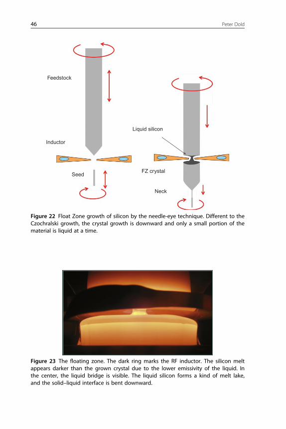
Liquid silicon
FZ crystalSeed
Inductor
Feedstock
Neck
Figure 22 Float Zone growth of silicon by the needle-eye technique. Different to theCzochralski growth, the crystal growth is downward and only a small portion of thematerial is liquid at a time.
Figure 23 The floating zone. The dark ring marks the RF inductor. The silicon meltappears darker than the grown crystal due to the lower emissivity of the liquid. Inthe center, the liquid bridge is visible. The liquid silicon forms a kind of melt lake,and the solid–liquid interface is bent downward.
46 Peter Dold
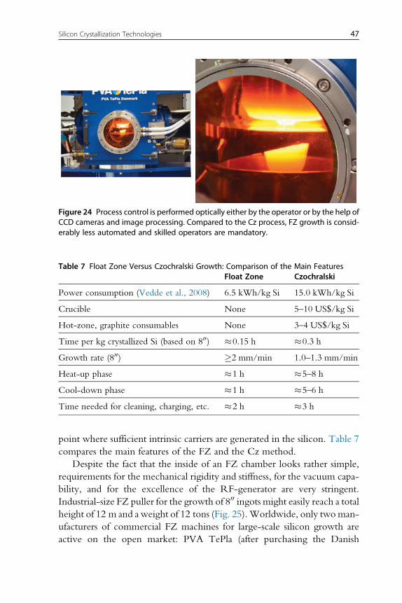
point where sufficient intrinsic carriers are generated in the silicon. Table 7
compares the main features of the FZ and the Cz method.
Despite the fact that the inside of an FZ chamber looks rather simple,
requirements for the mechanical rigidity and stiffness, for the vacuum capa-
bility, and for the excellence of the RF-generator are very stringent.
Industrial-size FZ puller for the growth of 800 ingots might easily reach a total
height of 12 m and a weight of 12 tons (Fig. 25).Worldwide, only twoman-
ufacturers of commercial FZ machines for large-scale silicon growth are
active on the open market: PVA TePla (after purchasing the Danish
Figure 24 Process control is performed optically either by the operator or by the help ofCCD cameras and image processing. Compared to the Cz process, FZ growth is consid-erably less automated and skilled operators are mandatory.
Table 7 Float Zone Versus Czochralski Growth: Comparison of the Main FeaturesFloat Zone Czochralski
Power consumption (Vedde et al., 2008) 6.5 kWh/kg Si 15.0 kWh/kg Si
Crucible None 5–10 US$/kg Si
Hot-zone, graphite consumables None 3–4 US$/kg Si
Time per kg crystallized Si (based on 800) �0.15 h �0.3 h
Growth rate (800) �2 mm/min 1.0–1.3 mm/min
Heat-up phase �1 h �5–8 h
Cool-down phase �1 h �5–6 h
Time needed for cleaning, charging, etc. �2 h �3 h
47Silicon Crystallization Technologies
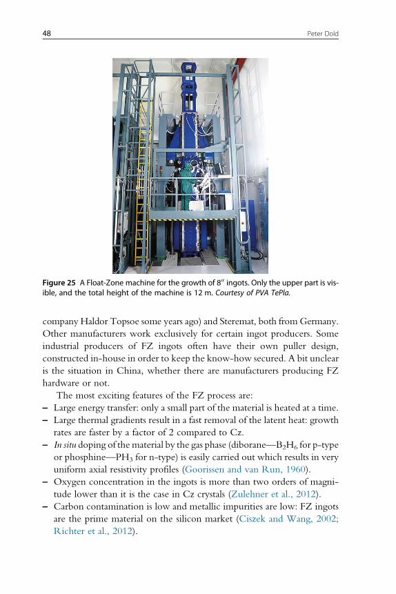
company Haldor Topsoe some years ago) and Steremat, both fromGermany.
Other manufacturers work exclusively for certain ingot producers. Some
industrial producers of FZ ingots often have their own puller design,
constructed in-house in order to keep the know-how secured. A bit unclear
is the situation in China, whether there are manufacturers producing FZ
hardware or not.
The most exciting features of the FZ process are:
– Large energy transfer: only a small part of the material is heated at a time.
– Large thermal gradients result in a fast removal of the latent heat: growth
rates are faster by a factor of 2 compared to Cz.
– In situ doping of the material by the gas phase (diborane—B2H6 for p-type
or phosphine—PH3 for n-type) is easily carried out which results in very
uniform axial resistivity profiles (Goorissen and van Run, 1960).
– Oxygen concentration in the ingots is more than two orders of magni-
tude lower than it is the case in Cz crystals (Zulehner et al., 2012).
– Carbon contamination is low and metallic impurities are low: FZ ingots
are the prime material on the silicon market (Ciszek and Wang, 2002;
Richter et al., 2012).
Figure 25 A Float-Zone machine for the growth of 800 ingots. Only the upper part is vis-ible, and the total height of the machine is 12 m. Courtesy of PVA TePla.
48 Peter Dold
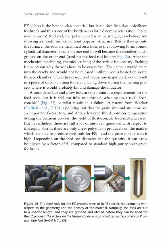
FZ silicon is the best-in-class material, but it requires first-class polysilicon
feedstock and this is one of the bottlenecks for FZ commercialization. To be
used as an FZ feed rod, the polysilicon has to be straight, crack-free, and
showing a smooth surface without popcorn structure. Before they go into
the furnace, the rods are machined on a lathe to the following form: round,
cylindrical diameter, a cone on one end (it will become the shoulder) and a
groove on the other end (used for the feed rod holder; Fig. 26). After the
mechanical machining, chemical etching of the surface is necessary. Etching
is one reason why the rods have to be crack-free. The etchant would creep
into the cracks and would not be released until the rod is heated up in the
furnace chamber. The other reason is obvious: any major crack could result
in a piece of silicon coming loose and falling down during the melting pro-
cess where it would probably hit and damage the inductor.
A smooth surface and a low bow are the minimum requirements for the
feed rods, but it is still not fully understood, what makes a rod “float-
zonable” (Fig. 27) or what results in a failure. A patent from Wacker
(Freiheit et al., 2010) is pointing out that the grain size and structure are
an important factor, too, and if they lowered the deposition temperature
during the Siemens process, the yield of float-zonable feed rods increased.
But nevertheless, there are still a lot of unsolved questions with respect to
this topic. Fact is, there are only a few polysilicon producers on the market
which are able to produce feed rods for FZ—and the price for the rods is
high. Depending on the feed rod diameter and the quantity, it can easily
be higher by a factor of 5, compared to standard high-purity solar-grade
feedstock.
Figure 26 The feed rods for the FZ process have to fulfill specific requirements withrespect to the geometry and the density of the material. Normally, the rods are cutto a specific length, and they are grinded and etched before they can be used forthe FZ process. The picture on the left-hand side was provided by courtesy of Silicon Prod-ucts Bitterfeld GmbH & Co. KG.
49Silicon Crystallization Technologies
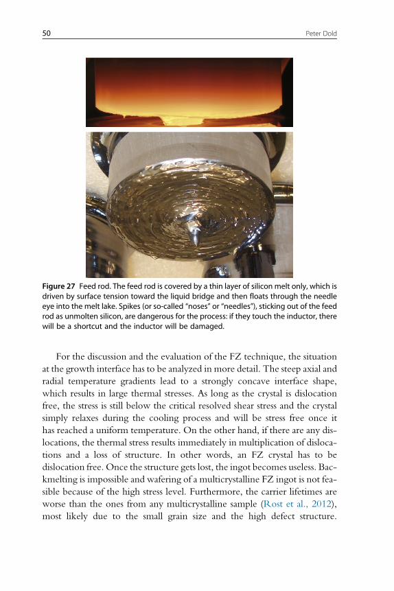
For the discussion and the evaluation of the FZ technique, the situation
at the growth interface has to be analyzed in more detail. The steep axial and
radial temperature gradients lead to a strongly concave interface shape,
which results in large thermal stresses. As long as the crystal is dislocation
free, the stress is still below the critical resolved shear stress and the crystal
simply relaxes during the cooling process and will be stress free once it
has reached a uniform temperature. On the other hand, if there are any dis-
locations, the thermal stress results immediately in multiplication of disloca-
tions and a loss of structure. In other words, an FZ crystal has to be
dislocation free. Once the structure gets lost, the ingot becomes useless. Bac-
kmelting is impossible and wafering of a multicrystalline FZ ingot is not fea-
sible because of the high stress level. Furthermore, the carrier lifetimes are
worse than the ones from any multicrystalline sample (Rost et al., 2012),
most likely due to the small grain size and the high defect structure.
Figure 27 Feed rod. The feed rod is covered by a thin layer of silicon melt only, which isdriven by surface tension toward the liquid bridge and then floats through the needleeye into the melt lake. Spikes (or so-called “noses” or “needles”), sticking out of the feedrod as unmolten silicon, are dangerous for the process: if they touch the inductor, therewill be a shortcut and the inductor will be damaged.
50 Peter Dold
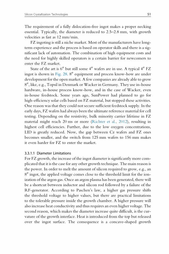
The requirement of a fully dislocation-free ingot makes a proper necking
essential. Typically, the diameter is reduced to 2.5–2.8 mm, with growth
velocities as fast as 12 mm/min.
FZ ingoting is still a niche market. Most of the manufacturers have long-
term experience and the process is based on operator skills and there is a sig-
nificant lack of automation. The combination of high equipment costs and
the need for highly skilled operators is a certain barrier for newcomers to
enter the FZ market.
State of the art is 600 but still some 400 wafers are in use. A typical 400 FZingot is shown in Fig. 28. 800 equipment and process know-how are under
development for the openmarket. A few companies are already able to grow
800, like, e.g., Topsil in Denmark orWacker in Germany. They use in-house
hardware, in-house process know-how, and in the case of Wacker, even
in-house feedstock. Some years ago, SunPower had planned to go for
high-efficiency solar cells based on FZ material, but stopped these activities.
One reason was that they could not secure sufficient feedstock supply. In the
early days, FZ wafers had always been the ultimate reference material for cell
testing. Depending on the resistivity, bulk minority carrier lifetime in FZ
material might reach 20 ms or more (Richter et al., 2012), resulting in
highest cell efficiencies. Further, due to the low oxygen concentrations,
LID is greatly reduced. Now, the gap between Cz wafers and FZ ones
becomes smaller, and the switch from 125 mm wafers to 156 mm makes
it even harder for FZ to enter the market.
3.3.1.1 Diameter LimitationsFor FZ growth, the increase of the ingot diameter is significantly more com-
plicated that it is the case for any other growth technique. The main reason is
the power. In order to melt the amount of silicon required to grow, e.g., an
800 ingot, the applied voltage comes close to the threshold limit for the ion-
ization of the argon gas. Once an argon plasma has been generated, there will
be a shortcut between inductor and silicon rod followed by a failure of the
RF-generator. According to Paschen’s law, a higher gas pressure shifts
the threshold voltage to higher values, but there are practical limitations
to the tolerable pressure inside the growth chamber. A higher pressure will
also increase heat conductivity and thus requires an even higher voltage. The
second reason, which makes the diameter increase quite difficult, is the cur-
vature of the growth interface. Heat is introduced from the top but released
over the ingot surface. The consequence is a concave-shaped growth
51Silicon Crystallization Technologies
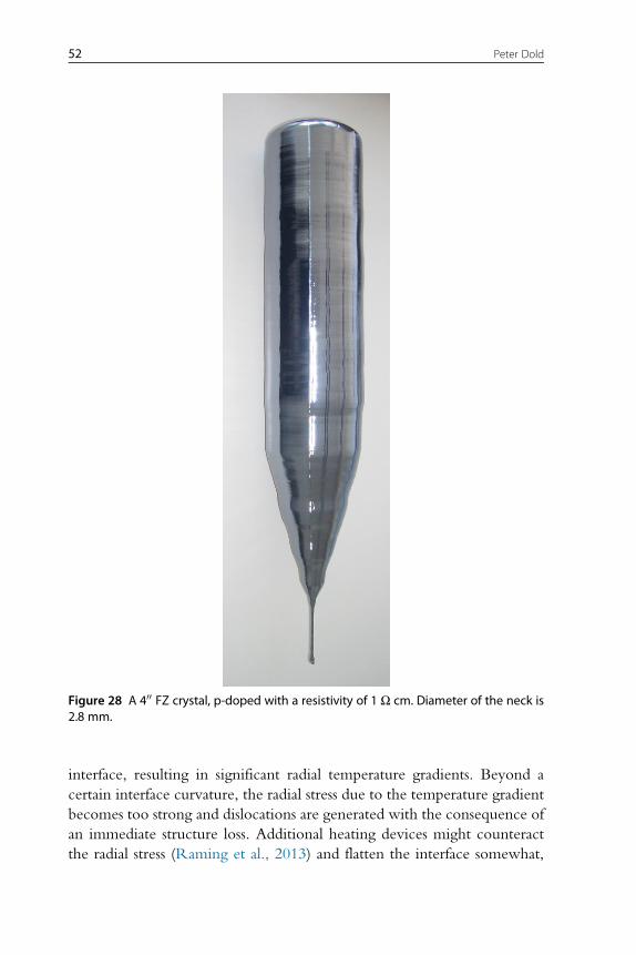
interface, resulting in significant radial temperature gradients. Beyond a
certain interface curvature, the radial stress due to the temperature gradient
becomes too strong and dislocations are generated with the consequence of
an immediate structure loss. Additional heating devices might counteract
the radial stress (Raming et al., 2013) and flatten the interface somewhat,
Figure 28 A 400 FZ crystal, p-doped with a resistivity of 1 Ω cm. Diameter of the neck is2.8 mm.
52 Peter Dold
but with the consequence that the heat loss is reduced and the growth rate
has to be lowered.
3.3.1.2 FeedstockAs mentioned in the beginning already, proper feed rods are absolutely
essential for successful FZ growth. In most cases, the feed rods are produced
by the Siemens technology, but the process differs from the standard
method. In order to get a crack-free rod with a good morphology and a
smooth surface, deposition rates are lower. Lower deposition rates mean
longer process times and thus higher energy costs. Still, only part of these
special feed rods can be sold for FZ growth, i.e., the straight part without
the bridge area and with a certain distance to the elbow and to the carbon
electrodes. Due to these reasons (and the fact that there are only a limited
number of producers able to handle the process properly), the price for
FZ feed rods is several times higher than it is the case for solar-grade poly-
silicon. Alternatives are under investigation.
One option reducing costs for FZ feed rods is the use of granular poly-
silicon from an FBR and feed it directly into an FZ furnace (von Ammon
and Altmannshofer, 2011; von Ammon et al., 2011a,b). The furnace looks a
bit different from a conventional one: a second inductor is implemented for
melting of the granules. Of course, special care is necessary that no granules
come close to the solid–liquid interface, or the structure would be lost
immediately. Further, the granular material has to be of high quality with
a low dust load and low metallic impurity levels.
Another option is the prepulling of the feed rods (so-called pp-FZ—
prepulled Float Zone): standard solar-grade polysilicon is melted in a cruci-
ble and, similar to the Cz process, a feed rod for the FZ process is pulled
(Dold et al., 2014b). Since the structure of the feed rod does not play a role,
the feed rods might be pulled with high velocity. Combining the prepulling
process with multipulling and other cost-reducing procedures, the ready-to-
use feed rod obtained from the prepulling process is quite cost competitive to
the Siemens process. The oxygen picked up during the prepulling process
will evaporate during the FZ process.
It is still anopenquestionwhetherFZwill ever play a significant role inPVor
not (of course besides the use of FZwafers in, e.g., Insulated-GateBipolarTran-
sistor (IGBTs) forPVinverters).Thedevelopmentofcommercial800 pullerswitha high degree of automation would be one step. Under these boundary condi-
tions, FZwould be a highly attractive alternative to Cz growth, considering the
lower operational costs, the high growth rates, and the excellent wafer quality.
53Silicon Crystallization Technologies
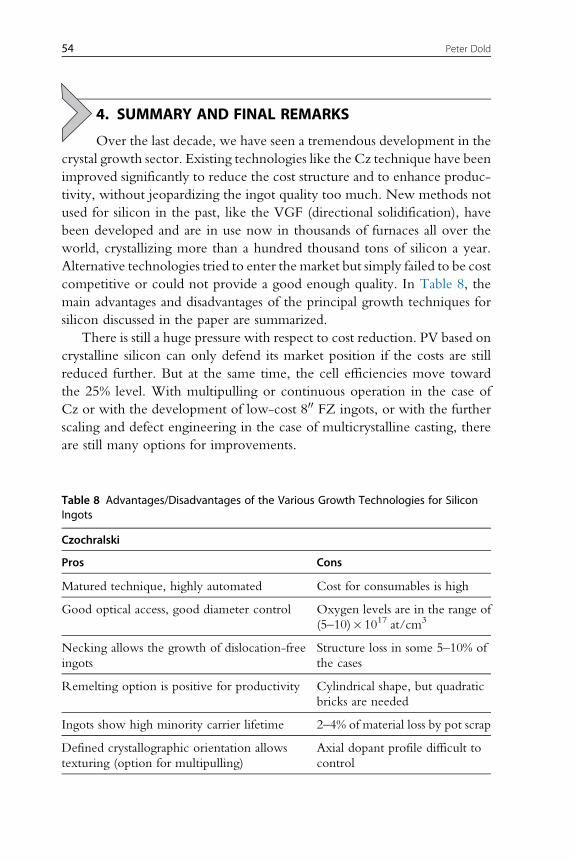
4. SUMMARY AND FINAL REMARKS
Over the last decade, we have seen a tremendous development in the
crystal growth sector. Existing technologies like the Cz technique have been
improved significantly to reduce the cost structure and to enhance produc-
tivity, without jeopardizing the ingot quality too much. New methods not
used for silicon in the past, like the VGF (directional solidification), have
been developed and are in use now in thousands of furnaces all over the
world, crystallizing more than a hundred thousand tons of silicon a year.
Alternative technologies tried to enter the market but simply failed to be cost
competitive or could not provide a good enough quality. In Table 8, the
main advantages and disadvantages of the principal growth techniques for
silicon discussed in the paper are summarized.
There is still a huge pressure with respect to cost reduction. PV based on
crystalline silicon can only defend its market position if the costs are still
reduced further. But at the same time, the cell efficiencies move toward
the 25% level. With multipulling or continuous operation in the case of
Cz or with the development of low-cost 800 FZ ingots, or with the further
scaling and defect engineering in the case of multicrystalline casting, there
are still many options for improvements.
Table 8 Advantages/Disadvantages of the Various Growth Technologies for SiliconIngots
Czochralski
Pros Cons
Matured technique, highly automated Cost for consumables is high
Good optical access, good diameter control Oxygen levels are in the range of
(5–10)�1017 at/cm3
Necking allows the growth of dislocation-free
ingots
Structure loss in some 5–10% of
the cases
Remelting option is positive for productivity Cylindrical shape, but quadratic
bricks are needed
Ingots show high minority carrier lifetime 2–4% of material loss by pot scrap
Defined crystallographic orientation allows
texturing (option for multipulling)
Axial dopant profile difficult to
control
54 Peter Dold

Table 8 Advantages/Disadvantages of the Various Growth Technologies for SiliconIngots—cont'd
Vertical gradient freeze
Pros Cons
Easy to handle, simple, and robust equipment Cost for consumables is high
Fully automated Carbon levels might reach
1�1018 at/cm3
Further scaling still possible Strong, nonuniform defect
structure
High kg/h ratio Impurity-rich side, top, and
bottom area
Decent oxygen level Impurity introduction by the
crucible/the coating
Relaxed feedstock requirements Axial dopant profile difficult to
control
Black-box operation, no in situ
control so far
Float Zone
Pros Cons
High growth rate Equipment costs are high
Good optical access, good diameter control Low degree of automation
Necking allows the growth of dislocation-free
ingots
Skilled operator required
Consumable cost is low, crucible-free, no
graphite
Cylindrical shape, but quadratic
bricks are needed
Ingots show very high minority carrier lifetime No backmelting in case of
structure loss
Defined crystallographic orientation allows
texturing
Diameter restricted to
approximately 800
Very low oxygen, <1016 at/cm3 Availability of feedstock
No losses by pot scrap
Uniform axial dopant profile is easy to realize
55Silicon Crystallization Technologies
REFERENCESAbe, K., Terashima, K., Matsumoto, T., Maeda, S., Nakanishi, H., 1998. Fused quartz dis-
solution rate in silicon melts: influence of boron addition. J. Cryst. Growth186, 557–564.
Alemany, C., Trassy, C., Pateyron, B., Li, K.-I., Delannoy, Y., 2002. Refining metallurgical-grade silicon by inductive plasma. Sol. Energy Mater. Cells 72, 41–48.
Altekruger, B., 1994. Apparatus for continuously feeding material to a melting, crucible.5,360,480.
Aulich, H., Schulze, F.W., 2009. Verfahren zur Herstellung von polykristallinenSiliziumstaben und polykristalliner Siliziumstab. DE 10 2007 041 803 A1.
Bender, D.L., 2013. Systems and processes for continuous growing of ingots. US2013/0133567 A1, 30.05.2013.
Bender, D.L., Smith, D.E.A., 2012.Weir design providing optimal purge gas flow, melt con-trol, and temperature stabilization for improved single crystal growth in a continuousCzochralski process. US 8,262,797 B1.
Bernreuter, J., 2014. The 2014 Who’s Who of Solar Silicon Production: BernreuterResearch Polysilicon Market Reports, p. 124.
Bernreuter, J., Haugwitz, F., 2010. TheWho’s Who of Solar Silicon Production: BernreuterResearch Polysilicon Market Reports, p. 174.
Birkmann, B., Kropfgans, F., 2013. Verfahren zur Herstellung eines gerichtet erstarrtenMaterialk€orpers, insbesondere eines Metall- oder Halbmetallk€orpers, sowieVerwendungen hiervon. DE 10 2012 102 597 A1, 26.09.2013.
Bohm, J., Ludge, A., Schr€oder, W., 1994. Crystal growth by floating zone melting.In: Hurle, D.T.J. (Ed.), Handbook of Crystal Growth vol. 2. Elsevier SciencePublishers, North-Holland, Amsterdam, London, New York, Tokyo, pp. 213–257.
Brandes, E.A., Brook, G.B., 1992. Smithells Metals Reference Book, seventh ed.Butterworth-Heinemann Ltd., London.
Ceccaroli, B., Friestad, K., 2005. Refining of metallurgical grade silicon. US 6,861,040 B1.Chaney, R.E., Varker, C.J., 1976. The dissolution rate of fused silica in molten silicon.
J. Cryst. Growth 33, 188–190.Ciszek, T.F., Wang, T.H., 2000. Silicon float-zone crystal growth as a tool for the study of
defects and impurities. High Purity Silicon Vi 4218, 105–117.Ciszek, T.F., Wang, T.H., 2002. Silicon defect and impurity studies using float-zone crystal
growth as a tool. J. Cryst. Growth 237, 1685–1691.Coletti, G., Geerligs, L.J., Manshanden, P., Swanson, C., Riepe, S., Warta, W.,
Arumughan, J., Kopecek, R., Oct. 2007. Impact of Iron and Molybdenum inMono and Multicrystalline Float-Zone Silicon Solar Cells. Solid State Phenomena131–133, 15–20.
Collet, Y., Magotte, O., VanDenBogaert, N., Rolinsky, R., Loix, F., Jacot, M., Regnier, V.,Marchal, J.-M., Dupret, F., 2012. Effective simulation of the effect of a transverse mag-netic field (TMF) in Czochralski silicon growth. J. Cryst. Growth 360, 18–24.
Czochralski, J., 1918. Ein neues Verfahren zur Messung der Kristallisationsgeschwindigkeitder Metalle. Z. Phys. Chem. 92, 219–221.
Dash, W.C., 1958. Silicon crystals free of dislocations. J. Appl. Phys. 29, 736–737.Dash, W.C., 1959. Growth of silicon crystals free from dislocations. J. Appl. Phys. 30 (4),
459–474.Davis Jr., J.R., Rohatgi, A., Hopkins, R.H., Blais, P.D., Rai-Choudhury, P.,
McCormick, J.R., Mollenkopf, H.C., 1980. Impurities in silicon solar cells. IEEE Trans.Electron Devices 27 (4), 677–687.
Delannoy, Y., Alemany, C., Li, K.-I., Proulx, P., Trassy, C., 2002. Plasma-refining processto provide solar-grade silicon. Sol. Energy Mater. Cells 72, 69–75.
56 Peter Dold
DeLuca, J.P., Delk, F.S., Johnson, B.K., Luter, W.L., Middendorf, N.D., Williams, D.S.,Ostrom, N.P., Highfill, J.N., 2012. Silicon single crystal doped with gallium, indium,or aluminum US2012/0056135 A1.
Dethloff, C., Friestad, K., 2007. Method for producing directionally solidified silicon ingots.WO 2007/001184 A1, 04.04.2007.
Dold, P., 2003. Czochralski growth of doped germanium with an applied rotating magneticfield. Cryst. Res. Technol. 38 (7–8), 659–668.
Dold, P., 2004. Analysis of microsegregation in RF-heated float zone growth of silicon—comparison to the radiation-heated process. J. Cryst. Growth 261, 1–10.
Dold, P., Benz, K.W., 1995. Convective temperature fluctuations in liquid gallium independence on static and rotating magnetic fields. Cryst. Res. Technol. 30 (8),1135–1145.
Dold, P., Ernst, M., Kunert, R., 2014a. In-situ measurement of the crystallization rate duringblock casting. In: 29th EU PVSEC Conference, Amsterdam, The Netherlands.
Dold, P., Zobel, F., Kunert, R., Lauer, K., Michl, B., 2014b. Low oxygen, high life-timewafers produced by a modified Float Zone process (pp-FZ). In: 29th EU PVSEC Con-ference, Amsterdam, The Netherlands.
Dosaj, V.D., Hunt, L.P., 1981. Method for producing solar-cell-grade silicon. 4,247,528,27.07.1981.
Fabry, L., Hesse, K., 2012. Crystalline silicon feedstock preparation and analysis.In: Willeke, G.P., Weber, E.R. (Eds.), Semiconductors and Semimetals, vol. 87.Elsevier Inc, pp. 185–261.
Forster, M., Fourmond, E., Einhaus, R., Lauvray, H., Kraiem, J., Lemiti, M., 2011. Gaco-doping in Cz-grown silicon ingots to overcome limitations of B andP compensated silicon feedstock for PV applications. Phys. Status Solidi C 8 (3),678–681.
Freiheit, H.C.D., Kraus, H., Sofin, M.D., 2010. Polykristalliner Siliciumstab fur das Zon-enschmelzverfahren und ein Verfahren zu dessen Herstellung. EP 1 992 593 B1,13.10.2010.
Galindo, V., Gerbeth, G., von Ammon, W., Tomzig, E., Virbulis, J., 2002. Crystal growthmelt flow control by means of magnetic fields. Energy Convers. Manag. 43, 309–316.
Geerligs, L.J., Wyers, G.P., Jensen, R., Raaness, O.,Waernes, A.N., Santen, S., Reinink, A.,Wiersma, B., 2002. Solar-grade silicon by a direct route based on carbothermic reductionof silica: requirements and production technology. In: Sopori, B.L. (Ed.), 12th Work-shop on Crystalline Silicon Solar Cell Materials and Processes, Breckenridge, CO.NREL National Renewable Energy Laboratory, Breckenridge, CO, pp. 215–218.
Glazov, V.M., Pashinkin, A.S., 2001. The thermophysical properties (heat capacity and ther-mal expansion) of single-crystalline silicon. High Temp. 39 (3), 413–419.
Goorissen, J., van Run, A.M.J.G., 1960. Gas-phase doping of silicon. In: The Institution ofElectrical Engineers, pp. 858–860, Paper No. 3022 E.
Gu, X., Yu, X., Guo, K., Chen, L.,Wang, D., Yang, D., 2012. Seed-assisted cast quasi-singlecrystalline silicon for photovoltaic application: towards high efficiency and low cost sil-icon solar cells. Sol. Energy Mater. Sol. Cells 101, 95–101.
Gunjai, P., Ramchandran, P., 2009. Tailoring oxygen distribution in 300 mm Czochralskicrystal of pure silicon using cusp magnetic field. In: Seventh International Conference onCFD in the Mineral and Process Industries CSIRO, 9–11 December 2009, Melbourne,Australia.
Gurvich, L.V., Vetyts, I.V., Alcock, C.B., 1990. Thermodynamic Properties of InorganicSubstances, vol. 2. Hemisphere, New York.
Heuer, M., 2013. Metallurgical grade and metallurgically refined silicon for photovoltaics.In: Willeke, G.P., Weber, E.R. (Eds.), Semiconductors and Semimetals, vol. 89.Elsevier Inc, pp. 77–134.
57Silicon Crystallization Technologies
Hirata, H., Hoshikawa, K., 1980. The dissolution rate of silica in molten silicon. Jpn. J. Appl.Phys. 19 (8), 1573–1574.
Hoshi, K., Isawa, N., Suzuki, T., Ohkubo, Y., 1985. Czochralski silicon crystals grown in atransverse magnetic field. J. Electrochem. Soc. 132 (3), 693–700.
Huang, X., Huang, M., Ding, C., Ming, I., 2013. Seed-assisted growth for high-qualitymulti-crystalline silicon ingots. In: CSSC-7, Fukuoka, Japan, pp. 91–96.
Hurle, D.T.J., Cockayne, B., 1994. Czochralski growth. In: Hurle, D.T.J. (Ed.), Handbookof Crystal Growth, vol. 2a. Elsevier Science Publishers, North-Holland, Amsterdam,London, New York, Tokyo, pp. 99–211.
Johnson, B.K., DeLuca, J.P., Luter, W.L. Silicon ingot having uniform multiple dopants andmethod and apparatus for producing same. US 2012/0301386 A1, 2012.
Kaes, M., Heuer, M., Kirscht, F., Turenne, A., Hofbauer, C., Jester, T., 2014. Metallurgi-cally purified silicon for photovoltaics 2AV.1.1. In: European PVSEC, Amsterdam.
Kajimoto, T., Horie, D., Sakurada, S., 1991. Method for growing silicon single crystal.5,037,503.
Kakimoto, K., 2002. Effects of rotating magnetic fields on temperature oxygen distributionin silicon melt. J. Cryst. Growth 237–239, 1785–1790.
Kakimoto, K., Shyo, T., Eguchi, M., 1995. Correlation between temperature and impurityconcentration fluctuations in silicon crystals grown by the Czochralski method. J. Cryst.Growth 151, 187–191.
Kakimoto, K., Yi, K.-W., Eguchi, M., 1996. Oxygen transfer during single silicon crystalgrowth in Czochralski system with vertical magnetic fields. J. Cryst. Growth163, 238–242.
Kanda, T., Hourai, M., Miki, S., Shigematsu, T., Tomokage, H., Miyano, T., Morita, H.,Shintani, A., 1996. Influence of melt-temperature fluctuations on striation formation inlarge-scale Czochralski Si growth systems. J. Cryst. Growth 166, 663–668.
Kaneko, K., 2010. Method for casting polycrystalline silicon. US 7,682,472 B2.Kaneko, K., Nakagawa, K., Onizuka, T., Sasatani, K., 2006. Recent status on electromag-
netic casting. NRELNational Renewable Energy Laboratory, (Ed.), 16thWorkshop onCrystalline Silicon Solar Cells andModules: Materials and Progresses, Denver, Colorado,pp. 2–7.
Kim, K.M., Smetana, P., 1985. Striations in CZ silicon crystals grown under various axialmagnetic field strengths. J. Appl. Phys. 58 (7), 2731–2735.
Kimbel, S.L., Chen, J., Schrenker, R., Ferry, L., 2012. Directional solidification furnace forreducing melt contamination and reducing wafer contamination. US8,317,920 B2.
Kirscht, F., Walerysiak, M., Heuer, M., Jouini, A., Ounadjela, K., 2010. Method and systemfor controlling resistivity in ingots made of compensated feedstock silicon. US 2010/0258768 A1.
Kobayashi, N., 1978. Computational simulation of the melt flow during Czochralski growth.J. Cryst. Growth 43, 357–363.
Kurz, M., Pusztai, A., Muller, G., 1999. Development of a new powerful computer codeCrysVUN++ especially designed for fast simulation of bulk crystal growth processes.J. Cryst. Growth 198/199, 101–106.
Lange, R.P., Jockel, D., Ziem, M., Rudolph, P., Kießling, F., Frank-Rotsch, C., Czupalla,M., Nacke, B., Kasjanow, H., 2008. Vorrichtung zur Herstellung von Kristallen auselektrisch leitenden Schmelzen. DE 10 2007 028 547 A1.
Leblanc, D., Boisvert, R., 2008. Process and apparatus for purifying low-grade siliconmaterial.
Li, Z.Y.Y., Liu, L.J., Ma,W.C., Kakimoto, K., 2011. Effects of argon flow on heat transfer ina directional solidification process for silicon solar cells. J. Cryst. Growth 318 (1),298–303.
58 Peter Dold
Li, T.F., Huang, H.C., Tsai, H.W., Lan, A., Chuck, C., Lan, C.W., 2012a. An enhancedcooling design in directional solidification for high quality multi-crystalline solar silicon.J. Cryst. Growth 340, 202–208.
Li, Z.Y., Liu, L.J., Liu, X., Zhang, Y.F., Xiong, J.F., 2012b. Effects of argon flow on meltconvection and interface shape in a directional solidification process for an industrial-sizesolar silicon ingot. J. Cryst. Growth 360, 87–91.
Lorenzini, R.E., Iwata, A., Lorenz, K., 1977. Continuous crystal growing furnace.4,036,595.
Lu, Z., 2007. Controlling melt-solid interface shape of a growing silicon crystal using variablemagnetic field. US 7,223,304 B2, May 29.
Ma, W.C., Zhong, G.X., Sun, L., Yu, Q.H., Huang, X.M., Liu, L.J., 2012. Influence of aninsulation partition on a seeded directional solidification process for quasi-single crystallinesilicon ingot for high-efficiency solar cells. Sol. Energy Mater. Sol. Cells 100, 231–238.
Mackintosha, B., Seidl, A., Ouellettea, M., Batheya, B., Yatesa, D., Kalejs, J., 2006. Largesilicon crystal hollow-tube growth by the edge-defined film-fed growth (EFG) method.J. Cryst. Growth 287, 428–432.
Melendez-Martınez, J.J., Domınguez-Rodrıguez, A., 2004. Creep of silicon nitride. Prog.Mater. Sci. 49, 19–107.
Morita, K., Yoshikawa, T., 2011. Thermodynamic evaluation of new metallurgical refiningprocesses for SOG-silicon production. Trans. NonferrousMetals Soc. China 21, 685–690.
Muller, A., Schwichtenberg, G., Leistner, J., Seidel, J., 2004. Vorrichtung sowie Verfahrenzur Uberwachung der Kristallisation eines Mediums, insbesondere Silizium. DE 10234 250 A1, 5.2.2004.
Muller, M., Sahr, U., Lentes, F., Bullesfeld, F., 2009. Verfahren und Vorrichtung zumKristallisieren eines Halbleitermaterials, insbesondere Silizium. DE 102008022882 A1.
Nichol, S., 2011. Method for purifying silicon. US 7,883,680.Oriwol, D., Mark, H., Wahl, B., 2013. Verfahren zur Herstellung von Silizium-Ingots. DE
10 2012 203 706 A1, 08.08.2013.Paetzold, U., Reisbeck, A., Surner, M., 2007. Process and apparatus for the hydrogenation of
chlorosilanes. US 2007/0073075 A1.Raming, G., Altmannshofer, L., Ratnieks, G., Landrichinger, J., Lobmeyer, J., Holzinger,
A., 2013. Method and apparatus for producing single crystals.Rancoule, G., 2012. Crucible for the crystallization of silicon and process for making the
same.REC Silicon Inc., 2013. White paper: benefit of FBR granular polysilicon to increase
efficiency of PV ingot manufacturing by increasing crucible polysilicon charge weight.In: FBR White Paper—V4 10/13, REC Webpage, pp. 1–8.
Reuschel, K., 1963. Vorrichtung zur Gewinnung reinsten kristallinen Halbleitermaterialsfuer elektrotechnische Zwecke. DE1155759 B, 17.10.1963.
Richter, A., Glunz, S.W., Werner, F., Schmidt, J., Cuevas, A., 2012. Improved quantitativedescription of Auger recombination in crystalline silicon. Phys. Rev. B 86 (16), 14.
Rodriguez, H., Guerrero, I., Koch, W., Endr€os, A., Franke, D., Hasler, C., Kalejs, J.,M€oller, H.J., 2011. Bulk crystal growth and wafering for PV. In: Luque, A.,Hegedus, S. (Eds.), Handbook of Photovoltaics: Science and Engineering, second ed.John Wiley & Sons, Ltd, pp. 218–264.
Rost, H.-J., Luedge, A., Riemann, H., Kirscht, F., Schulze, F.-W., 2012. Float zone (FZ)silicon: a potential material for advanced commercial solar cells? Cryst. Res. Technol.47 (3), 273–278.
Rudolph, P., Frank-Rotsch, C., Kiessling, F.M., Kudla, C., 2011. Current and next steps ofbulk crystal growth to meet the challenges of photovoltaics. J. Ceram. Process. Res.12, S159–S166.
59Silicon Crystallization Technologies
Schei, A., 1998. Method for refining of silicon. US 5,788,945.Schubert, M., Sch€on, J., Schindler, F., Kwapil, W., Abdollahinia, A., Michl, B., Riepe, S.,
Schmid, C., Schumann, M., Meyer, S., Warta, W., 2013. Impact of impurities from cru-cible and coating on mc-silicon quality—the example of iron and cobalt. IEEE J. Pho-tovoltaics 3 (4), 1250–1258.
Schumann, M., Meyer, S., Schmid, C., Haas, F., Riepe, S., Cr€oll, A., 2012. Impurity controlof quartz crucible coatings for directional solidification of silicon. In: 27th EuropeanPhotovoltaic Solar Energy Conference, Frankfurt, 24.–28.09.2012, Frankfurt, p. 5.
Schweickert, H., Reuschel, K., Gutsche, H., 1961. Production of high-purity semiconduc-tor materials for electrical purposes. US3011877 A, 05.12.1961.
Shimura, F., 2007. Single-crystal silicon: growth and properties. In: Kasap, S., Capper, P.(Eds.), Springer Handbook of Electronic and Photonic Materials. Springer, USA,pp. 255–269.
Sirtl, E., Hunt, L.P., Sawyer, D.H., 1974. High temperature reactions in the silicon-hydrogen-chlorine system. J. Electrochem. Soc. 121 (7), 919–925.
Smirnov, A.D., Kalaev, V.V., 2009. Analysis of impurity transport and deposition processeson the furnace elements during Cz silicon growth. J. Cryst. Growth 311, 829–832.
Stoddard, N., Wu, B., Witting, I., Wagener, M., Park, Y., Rozgonyi, G., Clark, R., 2008.Casting single crystal silicon: novel defect profiles from BP Solar’s Mono2 TM wafers.Solid State Phenom. 131–133, 1–8.
SUMCO Corporation, Annual Report, 2008, URL: http://www.sumcosi.com/english.Swaminathan, T.N., 2014a. Weir for improved crystal growth in a continuous Czochralski
process. US 2014/0144372 A1, 29.05.2014.Swaminathan, T.N., 2014b. Heat shield for improved continuous Czochralski process. US
2014/0144371 A1, 29.05.2014.Trempa, M., Reimann, C., Friedrich, J., Muller, G., 2010. The influence of growth rate on
the formation and avoidance of C and N related precipitates during directional solidifi-cation of multicrystalline silicon. J. Cryst. Growth 312, 1517–1524.
Tsai, H.W., Yang, M., Chuck, C., Lan, C.W., 2013. Effect of crucible coating on the graincontrol of multi-crystalline silicon crystal growth. J. Cryst. Growth 363, 242–246.
van Glabbeek, L., Atchley, B., Janoch, R.E., Anselmo, A.P., Reitsma, S., 2008. Method andapparatus for forming a silicon wafer. US2008/0102605 A1.
Vedde, J., Clausen, T., Borregaard, J., Kringhøj, P., 2008. Float Zone crystal growth forPV—where is the future? In: 23rd EU PVSEC, Valencia, Spain, 01.–04.09.2008, p. 3.
Virbulis, J., Wetzel, T., Muiznieks, A., Hanna, B., Dornberger, E., Tomzig, E.,Muhlbauer, A., Ammon, W.v., 2001. Numerical investigation of silicon melt flow inlarge diameter CZ-crystal growth under the influence of steady and dynamic magneticfields. J. Cryst. Growth 230, 92–99.
von Ammon,W., Altmannshofer, L., 2011a.Method for producing a single crystal composedof silicon using molten granules. US 2011/0185963 A1, 04.08.2011.
von Ammon, W., Altmannshofer, L., Wasner, M., 2011b. Method for producing a singlecrystal composed of silicon by remelting granules. US 2011a/0107960 A1, 12.05.2011.
von Ammon, W., Altmannshofer, L., Muiznieks, A., 2011b. Device for producing a singlecrystal composed of silicon by remelting granules. US 2011/0095018 A1, 28.04.2011.
Wakita, S., Tsuzukihashi, K., Ikeda, H., Kanai, M., 2013. Layered crucible for casting siliconingot and method of producing same. US 2013/0015318 A2.
Wang, X., 2014. Konca Solar Cell, personal communication.Wang, C., Zhang, H., Wang, T.H., Ciszek, T.F., 2003. A continuous Czochralski silicon
crystal growth system. J. Cryst. Growth 250, 209–214.Wang, Y., Ma,W., Morita, K., 2014. Removal of boron frommolten silicon by CaO-SiO2-
CaCl2 slag treatment. In: Øye, H.A., Brekken, H., Nygaard, L., Rong, H.M.,Tangstad, M., Tveit, H. (Eds.), Silicon for the Chemical and Solar Industry XII, Trond-heim, Norway, June 24–27, 2014, pp. 77–86.
60 Peter Dold
Watanabe, M., Eguchi, M., Hibiya, T., 1998. Flow and temperature field in molten siliconduring Czochralski crystal growth in a cusp magnetic field. J. Cryst. Growth193, 402–412.
Wetzel, T., Muiznieks, A., Muhlbauer, A., Gelfgat, Y., Gorbunov, L., Virbulis, J.,Tomzig, E., Ammon, W.v., 2001. Numerical model of turbulent CZ melt flow inthe presence of AC and CUSP magnetic fields and its verification in a laboratory facility.J. Cryst. Growth 230, 81–91.
Yang, Y.M., Yu, A., Hsu, B., Hsu,W.C., Yang, A., Lan, C.W., 2015. Development of high-performance multicrystalline silicon for photovoltaic industry. Prog. Photovolt. Res.Appl. 23, 340–351.
Ydstie, B.E., Du, J., 2011. Producing poly-silicon from silane in a fluidized bed reactor.In: Kosyachenko, L.A. (Ed.), Solar Cells—Silicon Wafer-Based Technologies,Available from: http://www.intechopen.com/books/solar-cells-silicon-wafer-based-technologies/producing-polysilicon-from-silane-in-a-fluidized-bed-reactor, ISBN:978-953-307-747-5. www.intechopen.com.
Yoshikawa, T., Arimura, K., Morita, K., 2005. Boron removal by titanium addition in solid-ification refining of silicon with Si-Al melt. Metall. Mater. Trans. B 36 (6), 837–842.
Zulehner, W., 1982. Device and process for pulling high-purity semiconductor rods from amelt. 4,330,362.
Zulehner, W., 1999. Historical overview of silicon crystal pulling development. In: E-MRSSpring Meeting, Strasbourg, France, Symposium E—Advances in Silicon Substrates,Conference proceedings.
Zulehner, W., Huber, D., 1982. Czochralski-grown silicon. In: Grabmeier, J. (Ed.), CrystalsGrowth, Properties, and Applications, vol. 8. Springer, Berlin, Heidelberg, New York,pp. 3–143.
Zulehner, W., Neuer, B., Rau, G., 2012. Silicon. In: Ullmann´s Encyclopedia of IndustrialChemistry, vol. 32. Wiley-VCH Verlag GmbH &Co. KGaA, Weinheim, pp. 573–601.
61Silicon Crystallization Technologies

This page intentionally left blank
CHAPTER TWO
Wafering of SiliconHans Joachim M€oller1Fraunhofer Technology Center for Semiconductor Materials, Freiberg, Germany1Corresponding author: e-mail address: [email protected]
Contents
1. Introduction 632. Multiwire Sawing Technology 65
2.1 Slurry-Based Sawing 662.2 Fixed Abrasive Sawing 692.3 Experimental Sawing Results 712.4 Determination of Wafer Properties 802.5 Electronic Grade Silicon 89
3. Basic Sawing Mechanisms 903.1 Slurry-Based Sawing 903.2 Damage of the Wafer Surface 99
4. Alternative Wafering Technologies 1024.1 Cleavage Technologies 1024.2 Layer Transfer Technologies 103
References 105
1. INTRODUCTION
Multiwire sawing has been developed as the main wafer-slicing tech-
nique for large multi- and monocrystalline silicon crystals in the photovol-
taic industry. The advantages are a high yield in production and a goodwafer
quality even for thin wafers. Since 80% of today’s solar cell production is
based on crystalline silicon material, one can expect that multiwire sawing
will remain an important processing technology (Fig. 1). In the past decade,
the technology has also been introduced into the microelectronics industry
because it also has advantages there.
The cost pressure on the wafer fabrication is, however, high because the
production of wafers for solar cells has a cost share of about 15% of the final
module cost (International Technology Roadmap for Photovoltaic, 2012).
One of the reasons is that wire sawing needs expensive supply materials and
Semiconductors and Semimetals, Volume 92 # 2015 Elsevier Inc.ISSN 0080-8784 All rights reserved.http://dx.doi.org/10.1016/bs.semsem.2015.02.003
63

is still accompanied by a substantial loss of high-quality silicon. Because of its
high cost share, the sawing process can contribute considerably to the overall
cost reduction if one can improve the technology.
Significant advances have already been made. The module prices
dropped by 20% every year which is typical for a growing and upscaling
industry (Global Market Outlook, 2012). Current prices for modules are
already considerably below 1 €/Wp, which is considered the grid parity
limit, where the electricity prices per kWh become comparable to the con-
sumer prices in Germany.
The photovoltaic market, which is the main driving force for the mul-
tiwire technology, is expected to grow continuously over the next decades
with further cost reductions. Although the enormous growth with growth
rates up to 40% over the past 10 years has been interrupted in 2012, one
expects, after market purification, a moderate growth over the next years.
The requirements on wafers for the microelectronic industry are different;
cost reduction is, however, also an issue there.
The sawing process depends on many variable parameters, which makes
it difficult to optimize the process in view of throughput, reduction of mate-
rial losses, reduction of supply materials, and wafer surface quality. Most of
the progress has been made by experience and improved machine
Figure 1 Annual development of the worldwide market shares of solar cell technolo-gies (Solar PV Market Forecast, 2012).
64 Hans Joachim M€oller

technology. Further progress needs, however, a more basic knowledge
about the microscopic details of the sawing process in order to slice crystals
in a controlled way. This is particularly the case when the wafer thickness
will be reduced further in the future. Although current wafer thicknesses
remained around 180 μm for some years, one expects a further reduction
eventually down to 100 μm because one can obtain more wafers from
the expensive silicon crystals (see Fig. 2). In the following, the principles
of the sawing process will be described as far as they are understood today.
2. MULTIWIRE SAWING TECHNOLOGY
Today, two techniques are currently used to grow large silicon crys-
tals: the growth of round monocrystals and the growth of square-shaped
multicrystals. After removing the side and end parts of the crystals, mostly
by band saws, the crystals are then cut into wafers using multiwire saws.
Worldwide, only very few companies have developedmultiwire saws which
can fulfill the current requirements of the industry. The companies with the
largest market shares are located in Switzerland, Japan, and the United States.
Figure 3 shows a typical industry multiwire saw, where the cutting area is in
the front part of the machine.
The principle of a multiwire saw is shown in Fig. 4. A single wire is sup-
plied by a spool (not shown here), wound several hundred times around 2–4
wire guide rollers (depending on the machine type and the manufacturer),
and picked up on the other side by another spool (also not shown).
Figure 2 Annual development of the thickness of commercial silicon solar cells(International Technology Roadmap, 2012).
65Wafering of Silicon

Depending on the wire guide arrangement, between 1 and 4 ingots can be
cut at the same time. The wires are made from steel and have a thickness
between 100 and 130 μm today. New steel wires are usually covered with
a thin brass layer from the wire drawing process, which has no function and
is quickly removed during sawing. The wire guide rollers have grooves
which guide the wires and keep them at a defined distance. The groove dis-
tance, the wire diameter, and the abrasive particle size determine the final
thickness of the wafers.
2.1 Slurry-Based SawingToday’s dominant sawing technique uses saws, where the cutting is achieved
by free-floating abrasive particles, which are suspended in a carrier fluid
(loose abrasive sawing). The suspension or slurry is supplied through nozzles
on the wire web and carried by the wires into the sawing channel.
Figure 3 Example of an industrial multiwire sawing machine (Applied Materials; HCTE 500 SD).
Figure 4 Principle of different wire guide arrangements of multiwire saws (Assi, 2013).
66 Hans Joachim M€oller
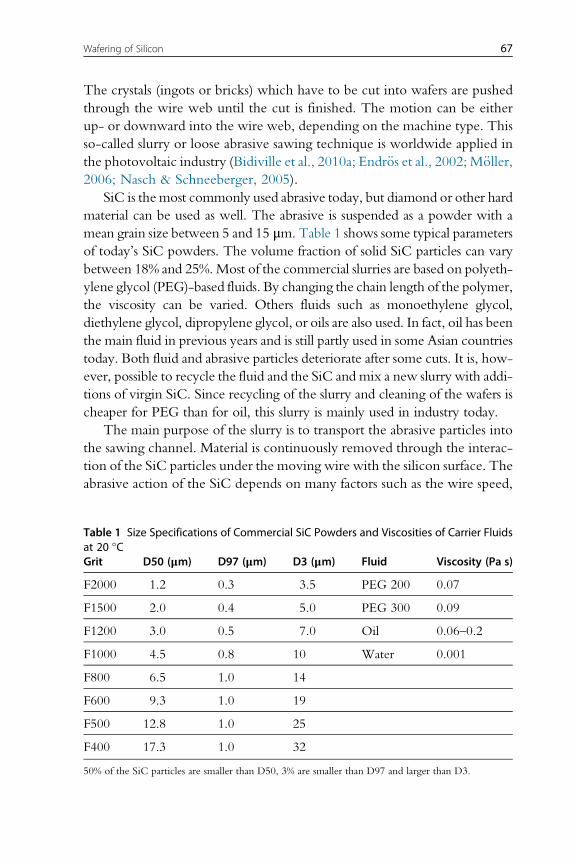
The crystals (ingots or bricks) which have to be cut into wafers are pushed
through the wire web until the cut is finished. The motion can be either
up- or downward into the wire web, depending on the machine type. This
so-called slurry or loose abrasive sawing technique is worldwide applied in
the photovoltaic industry (Bidiville et al., 2010a; Endr€os et al., 2002; M€oller,2006; Nasch & Schneeberger, 2005).
SiC is themost commonly used abrasive today, but diamond or other hard
material can be used as well. The abrasive is suspended as a powder with a
mean grain size between 5 and 15 μm. Table 1 shows some typical parameters
of today’s SiC powders. The volume fraction of solid SiC particles can vary
between 18% and 25%.Most of the commercial slurries are based on polyeth-
ylene glycol (PEG)-based fluids. By changing the chain length of the polymer,
the viscosity can be varied. Others fluids such as monoethylene glycol,
diethylene glycol, dipropylene glycol, or oils are also used. In fact, oil has been
the main fluid in previous years and is still partly used in some Asian countries
today. Both fluid and abrasive particles deteriorate after some cuts. It is, how-
ever, possible to recycle the fluid and the SiC and mix a new slurry with addi-
tions of virgin SiC. Since recycling of the slurry and cleaning of the wafers is
cheaper for PEG than for oil, this slurry is mainly used in industry today.
The main purpose of the slurry is to transport the abrasive particles into
the sawing channel. Material is continuously removed through the interac-
tion of the SiC particles under the moving wire with the silicon surface. The
abrasive action of the SiC depends on many factors such as the wire speed,
Table 1 Size Specifications of Commercial SiC Powders and Viscosities of Carrier Fluidsat 20 °CGrit D50 (μm) D97 (μm) D3 (μm) Fluid Viscosity (Pa s)
F2000 1.2 0.3 3.5 PEG 200 0.07
F1500 2.0 0.4 5.0 PEG 300 0.09
F1200 3.0 0.5 7.0 Oil 0.06–0.2
F1000 4.5 0.8 10 Water 0.001
F800 6.5 1.0 14
F600 9.3 1.0 19
F500 12.8 1.0 25
F400 17.3 1.0 32
50% of the SiC particles are smaller than D50, 3% are smaller than D97 and larger than D3.
67Wafering of Silicon
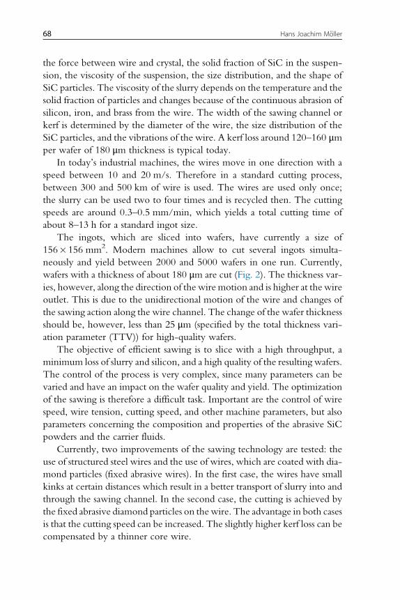
the force between wire and crystal, the solid fraction of SiC in the suspen-
sion, the viscosity of the suspension, the size distribution, and the shape of
SiC particles. The viscosity of the slurry depends on the temperature and the
solid fraction of particles and changes because of the continuous abrasion of
silicon, iron, and brass from the wire. The width of the sawing channel or
kerf is determined by the diameter of the wire, the size distribution of the
SiC particles, and the vibrations of the wire. A kerf loss around 120–160 μmper wafer of 180 μm thickness is typical today.
In today’s industrial machines, the wires move in one direction with a
speed between 10 and 20 m/s. Therefore in a standard cutting process,
between 300 and 500 km of wire is used. The wires are used only once;
the slurry can be used two to four times and is recycled then. The cutting
speeds are around 0.3–0.5 mm/min, which yields a total cutting time of
about 8–13 h for a standard ingot size.
The ingots, which are sliced into wafers, have currently a size of
156�156 mm2. Modern machines allow to cut several ingots simulta-
neously and yield between 2000 and 5000 wafers in one run. Currently,
wafers with a thickness of about 180 μm are cut (Fig. 2). The thickness var-
ies, however, along the direction of the wire motion and is higher at the wire
outlet. This is due to the unidirectional motion of the wire and changes of
the sawing action along the wire channel. The change of the wafer thickness
should be, however, less than 25 μm (specified by the total thickness vari-
ation parameter (TTV)) for high-quality wafers.
The objective of efficient sawing is to slice with a high throughput, a
minimum loss of slurry and silicon, and a high quality of the resulting wafers.
The control of the process is very complex, since many parameters can be
varied and have an impact on the wafer quality and yield. The optimization
of the sawing is therefore a difficult task. Important are the control of wire
speed, wire tension, cutting speed, and other machine parameters, but also
parameters concerning the composition and properties of the abrasive SiC
powders and the carrier fluids.
Currently, two improvements of the sawing technology are tested: the
use of structured steel wires and the use of wires, which are coated with dia-
mond particles (fixed abrasive wires). In the first case, the wires have small
kinks at certain distances which result in a better transport of slurry into and
through the sawing channel. In the second case, the cutting is achieved by
the fixed abrasive diamond particles on the wire. The advantage in both cases
is that the cutting speed can be increased. The slightly higher kerf loss can be
compensated by a thinner core wire.
68 Hans Joachim M€oller

2.2 Fixed Abrasive SawingMost of the industrial multiwire saws today can also be used with fixed abra-
sive wires. The technique itself has been used for a long time to cut hard
materials such as sapphire crystals. The slurry is replaced here by a coolant
fluid such as water, which is also cheaper. One also needs less wire.
Recent developments have shown that it can also be used to cut silicon
wafers (Aoyama et al., 2009; Bidiville et al., 2009; Bye et al., 2009; Proventa
et al., 2012). The requirements on the wafer quality in the photovoltaic
industry are, however, different compared for instance to sapphire. Wafers
and wires have to be much thinner to reduce the loss of expensive silicon
material. The quality of the wafer surface, which is determined by the
roughness, TTV, and the subsurface damage, has to be high and at least com-
parable to conventionally sawn wafers. Furthermore, there must be a cost
advantage. Since the diamond-coated wires are at present still more than
50 times more expensive (about 70–100 €/km), one has to reduce cost
by higher sawing speeds and multiple use of the wires. The goal here is a
cost reduction of more than 20% and at least maintaining the present wafer
qualities. Up to now, the technology has not been introduced into the high
volume production PV market. An exception is Japan, where fixed abrasive
sawing has already a market share (Solar Battery Technologies, 2012). The
higher cost of the fixed abrasive wires prevented so far the worldwide use of
the technique.
Figure 5 shows the surface of such a wire with fixed diamond particles.
There are three techniques to fix the particles on the surface: resin bonding,
electroplating bonding, and blazing. Only the first two are currently consid-
ered. Resin bonding is cheaper to manufacture but the particles are less
strongly bonded. Therefore, the wires cannot be loaded as much which
reduces the performance. In the electroplating technique, the particles are
embedded in a nickel-coating layer, which gives a stronger bond, but at
Figure 5 Steel wire coated with diamond particles (electroplating) (Buchwald et al.,2013a).
69Wafering of Silicon
the expense of the cost. One can expect, however, that a mass production of
such wires will reduce the wire cost substantially.
In fixed abrasive sawing, the machines are operated in the so-called pil-
grim mode, where the wire is running back and forth. Typically, the wire is
running for several hundred meters in one direction before it is stopped and
the motion direction is reversed. In each cycle, a few meters of new wire are
added in one direction.
Since higher cutting speeds can be achieved (>1 mm/min), the cutting
times are reduced to 2–3 h. The wire consumption is about 5 km then and
thus very much reduced.Many of the current industrial saws allow highwire
and cutting speeds. The sawing machines therefore require only slight mod-
ifications to operate it with the diamond-coated wires. These modifications
mainly require a change of the fluid supply system. Since the fluid in a dia-
mond wire machine has the function to cool the ingot and clean the wire,
one only has to modify the nozzle system in the saw slightly.
The competiveness of the fixed abrasive technique depends on the cost
per wafer. In recent years, the cost of the fixed abrasive wires could already
be reduced, but other factors are also important. During sawing, the wafer
surface is damaged, as will be discussed in Section 2.3 in detail. This reduces
the mechanical stability of the wafers, which is important for the following
processing steps of the wafers such as cleaning, solar cell processing, and
module manufacturing. With increasing cutting speeds, the wafers become
more unstable and the wafer yield is reduced.
The experiences so far indicate that fixed abrasive sawing is able to cut
monocrystalline ingots into wafers of standard thickness of 180 μm. The
wafer surface quality is good but may require an adjustment of the following
etching processes for texturization and further solar cell processes. The
results also show that sawing multicrystalline wafers works less well
(Buchwald et al., 2013b, 2014). The wafer surface quality is lower and wafer
breakage is more frequent. The reasons for these differences between mono-
andmulticrystalline silicon will be discussed in Section 2.3. Such a difference
between the two materials is not observed for slurry-based sawing.
Considering the long-term industrial development, wafers of less than
100 μm may be required in the future. At present, such thin wafers cannot
be handled in the downstream process of solar cell and module fabrication.
Thinner wafers require adapted solar cell designs because they absorb less
light. Such processes have not been implemented into the standard produc-
tion chain. In addition, the following industrial processing steps, which
70 Hans Joachim M€oller
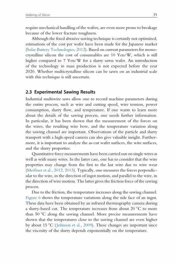
require mechanical handling of the wafers, are even more prone to breakage
because of the lower fracture toughness.
Although the fixed abrasive sawing technique is certainly not optimized,
estimations of the cost per wafer have been made for the Japanese market
(Solar Battery Technologies, 2012). Based on current parameters for mono-
crystalline silicon the cost of consumables are 10 Yen/W, which is still
higher compared to 7 Yen/W for a slurry sawn wafer. An introduction
of the technology in mass production is not expected before the year
2020. Whether multicrystalline silicon can be sawn on an industrial scale
with this technique is still uncertain.
2.3 Experimental Sawing ResultsIndustrial multiwire saws allow one to record machine parameters during
the entire process, such as wire and cutting speed, wire tension, power
consumption, slurry flow, and temperature. If one wants to learn more
about the details of the sawing process, one needs further information.
In particular, it has been shown that the measurement of the forces on
the wires, the resulting wire bow, and the temperature variation along
the sawing channel are important. Observations of the particle and slurry
transport with a high-speed camera can also give valuable insight. Further-
more, it is important to analyze the as-cut wafer surfaces, the wire surfaces,
and the slurry properties.
Quantitative forcemeasurements have been carried out on single wires as
well as with many wires. In the latter case, one has to consider that the wire
properties may change from the first to the last wire due to wire wear
(Meißner et al., 2012, 2013). Typically, one measures the forces perpendic-
ular to the wire, in the direction of ingot motion, and parallel to the wire, in
the direction of wire motion. The latter gives the friction force of the sawing
process.
Due to the friction, the temperature increases along the sawing channel.
Figure 6 shows the temperature variations along the side face of an ingot.
These data have been obtained by an infrared thermography camera during
a slurry-based cut. The temperature increases from about 20 °C to more
than 50 °C along the sawing channel. More precise measurements have
shown that the temperatures close to the sawing channel are even higher
by about 15 °C ( Johnsen et al., 2009). These changes are important since
the viscosity of the slurry depends exponentially on the temperature.
71Wafering of Silicon
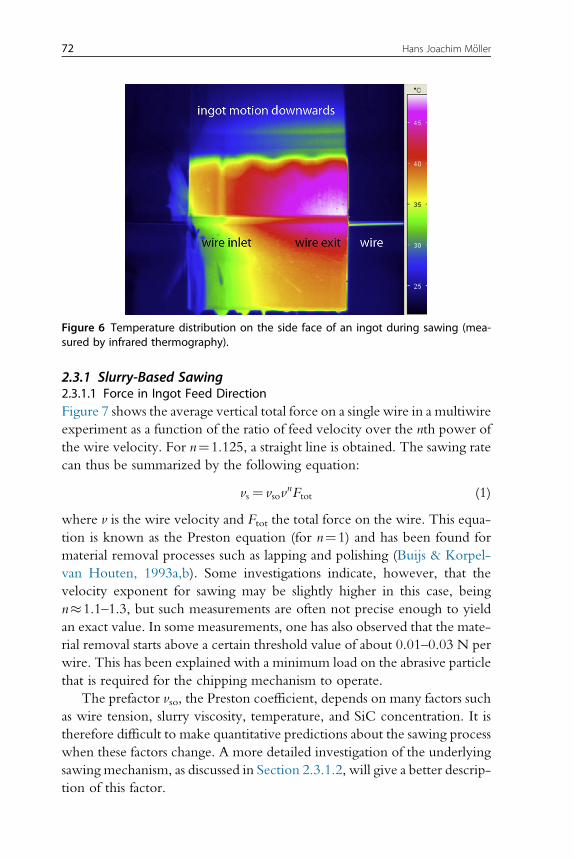
2.3.1 Slurry-Based Sawing2.3.1.1 Force in Ingot Feed DirectionFigure 7 shows the average vertical total force on a single wire in a multiwire
experiment as a function of the ratio of feed velocity over the nth power of
the wire velocity. For n¼1.125, a straight line is obtained. The sawing rate
can thus be summarized by the following equation:
vs ¼ vsovnFtot (1)
where v is the wire velocity and Ftot the total force on the wire. This equa-
tion is known as the Preston equation (for n¼1) and has been found for
material removal processes such as lapping and polishing (Buijs & Korpel-
van Houten, 1993a,b). Some investigations indicate, however, that the
velocity exponent for sawing may be slightly higher in this case, being
n�1.1–1.3, but such measurements are often not precise enough to yield
an exact value. In some measurements, one has also observed that the mate-
rial removal starts above a certain threshold value of about 0.01–0.03 N per
wire. This has been explained with a minimum load on the abrasive particle
that is required for the chipping mechanism to operate.
The prefactor vso, the Preston coefficient, depends on many factors such
as wire tension, slurry viscosity, temperature, and SiC concentration. It is
therefore difficult to make quantitative predictions about the sawing process
when these factors change. A more detailed investigation of the underlying
sawing mechanism, as discussed in Section 2.3.1.2, will give a better descrip-
tion of this factor.
Figure 6 Temperature distribution on the side face of an ingot during sawing (mea-sured by infrared thermography).
72 Hans Joachim M€oller
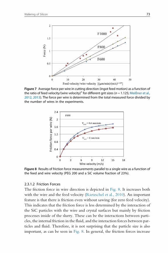
2.3.1.2 Friction ForcesThe friction force in wire direction is depicted in Fig. 8. It increases both
with the wire and the feed velocity (Rietzschel et al., 2010). An important
feature is that there is friction even without sawing (for zero feed velocity).
This indicates that the friction force is less determined by the interaction of
the SiC particles with the wire and crystal surfaces but mainly by friction
processes inside of the slurry. These can be the interactions between parti-
cles, the internal friction in the fluid, and the interaction forces between par-
ticles and fluid. Therefore, it is not surprising that the particle size is also
important, as can be seen in Fig. 8. In general, the friction forces increase
Figure 7 Average force per wire in cutting direction (ingot feedmotion) as a function ofthe ratio of feed velocity/(wire velocity)n for different grit sizes (n¼1.125; Meißner et al.,2012, 2013). The force per wire is determined from the total measured force divided bythe number of wires in the experiments.
Figure 8 Results of friction force measurements parallel to a single wire as a function ofthe feed and wire velocity (PEG 200 and a SiC volume fraction of 23%).
73Wafering of Silicon
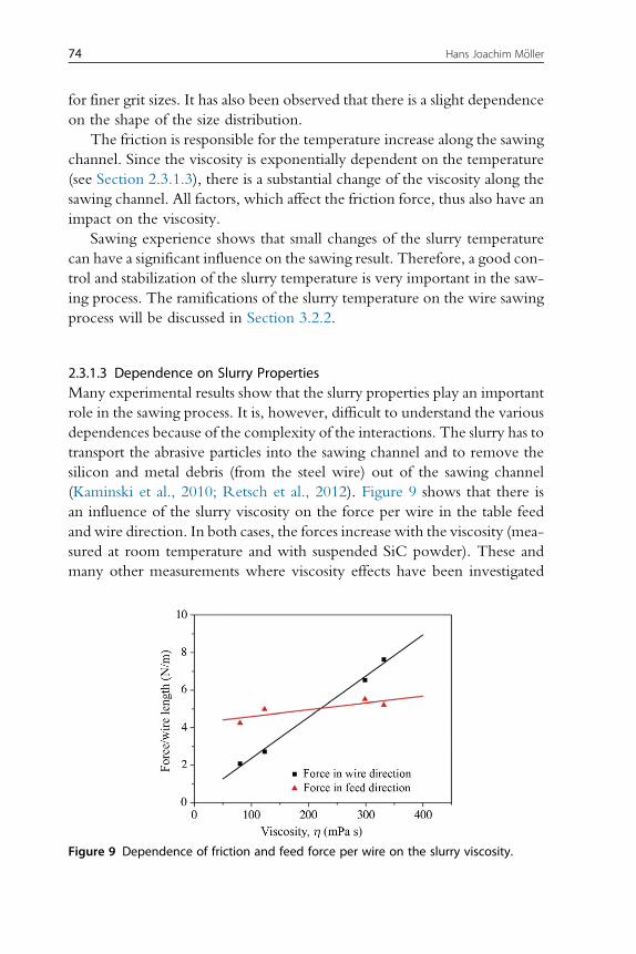
for finer grit sizes. It has also been observed that there is a slight dependence
on the shape of the size distribution.
The friction is responsible for the temperature increase along the sawing
channel. Since the viscosity is exponentially dependent on the temperature
(see Section 2.3.1.3), there is a substantial change of the viscosity along the
sawing channel. All factors, which affect the friction force, thus also have an
impact on the viscosity.
Sawing experience shows that small changes of the slurry temperature
can have a significant influence on the sawing result. Therefore, a good con-
trol and stabilization of the slurry temperature is very important in the saw-
ing process. The ramifications of the slurry temperature on the wire sawing
process will be discussed in Section 3.2.2.
2.3.1.3 Dependence on Slurry PropertiesMany experimental results show that the slurry properties play an important
role in the sawing process. It is, however, difficult to understand the various
dependences because of the complexity of the interactions. The slurry has to
transport the abrasive particles into the sawing channel and to remove the
silicon and metal debris (from the steel wire) out of the sawing channel
(Kaminski et al., 2010; Retsch et al., 2012). Figure 9 shows that there is
an influence of the slurry viscosity on the force per wire in the table feed
and wire direction. In both cases, the forces increase with the viscosity (mea-
sured at room temperature and with suspended SiC powder). These and
many other measurements where viscosity effects have been investigated
Figure 9 Dependence of friction and feed force per wire on the slurry viscosity.
74 Hans Joachim M€oller

are, however, difficult to analyze because the correct determination of the
viscosity is not completely clear at present.
Standard practice is the measurement with conventional viscosimeters,
which determine the viscosity for shear velocities, which are, however,
about a factor thousand smaller than the ones which occur in the sawing
channel. Recent measurements at these high shear rates indicate that the vis-
cosity decreases to some extent, but systematic measurements are not avail-
able today (Anspach & Schulze, 2007).
A second factor that has to be considered is the change of the carrier fluid
viscosity with the volume fraction of the solid material that is suspended in
the fluid. This is depicted in Fig. 10 for different slurries with SiC loading.
The general trend is that with increasing volume fraction ϕ, the viscosity ηincreases. One can also see that a smaller grit size increases the viscosity as
well. In general, the dependence can be approximated by the Krieger–
Dougherty relationship
η¼ ηo 1� ϕ
ϕo
� ��q
(2)
if appropriate parameters are selected for ϕo and q. ηo is the viscosity of thecarrier fluid (Struble & Sun, 1993). The experimental data given here yield a
value of q�1.
Figure 10 Relative viscosity as a function of the volume fraction of SiC in a PEG 300carrier fluid for different grit size distributions. The solid lines are Krieger–Dougherty fitswith appropriate parameters.
75Wafering of Silicon
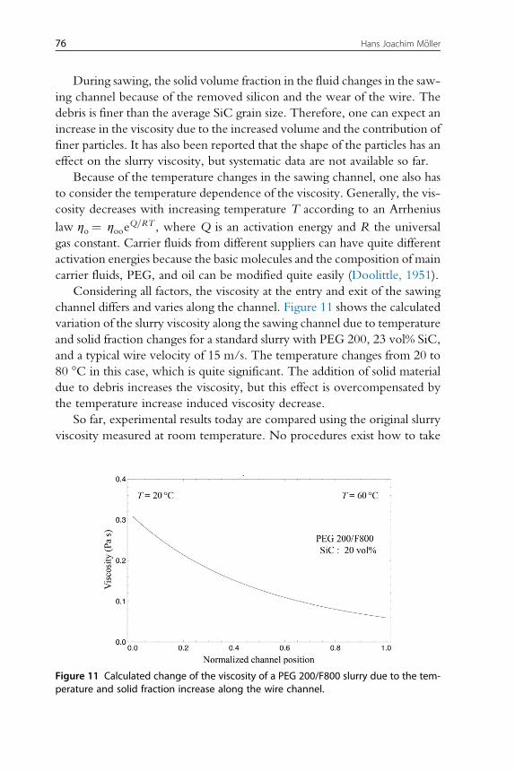
During sawing, the solid volume fraction in the fluid changes in the saw-
ing channel because of the removed silicon and the wear of the wire. The
debris is finer than the average SiC grain size. Therefore, one can expect an
increase in the viscosity due to the increased volume and the contribution of
finer particles. It has also been reported that the shape of the particles has an
effect on the slurry viscosity, but systematic data are not available so far.
Because of the temperature changes in the sawing channel, one also has
to consider the temperature dependence of the viscosity. Generally, the vis-
cosity decreases with increasing temperature T according to an Arrhenius
law ηo¼ ηooeQ=RT , where Q is an activation energy and R the universal
gas constant. Carrier fluids from different suppliers can have quite different
activation energies because the basic molecules and the composition of main
carrier fluids, PEG, and oil can be modified quite easily (Doolittle, 1951).
Considering all factors, the viscosity at the entry and exit of the sawing
channel differs and varies along the channel. Figure 11 shows the calculated
variation of the slurry viscosity along the sawing channel due to temperature
and solid fraction changes for a standard slurry with PEG 200, 23 vol% SiC,
and a typical wire velocity of 15 m/s. The temperature changes from 20 to
80 °C in this case, which is quite significant. The addition of solid material
due to debris increases the viscosity, but this effect is overcompensated by
the temperature increase induced viscosity decrease.
So far, experimental results today are compared using the original slurry
viscosity measured at room temperature. No procedures exist how to take
Figure 11 Calculated change of the viscosity of a PEG 200/F800 slurry due to the tem-perature and solid fraction increase along the wire channel.
76 Hans Joachim M€oller
into account the various factors that cause viscosity changes along the sawing
channel and how to determine a relevant viscosity value correctly. Since the
influence of the slurry on the sawing performance is a key factor today, fur-
ther research is required to better understand the role of the slurry in the
sawing process.
2.3.1.4 Wire TensionThe control of the wire tension is very essential in the sawing process, both
to prevent wire breakage and to guarantee stable sawing conditions. The
sawingmachines have therefore sophisticated control mechanisms. Thewire
tension is kept constant before and behind the wire web, mostly between
20 and 25 N. Changes of the wire tensions between the wire guide rollers
in the cutting area cannot be controlled. Recent investigations have shown
that the wire tension is actually reduced from the first to the last wire in the
web due to two effects (Meißner et al., 2012, 2013). During the first 50 mm
in the wire web, the wire is plastically deformed by about 0.25%. It could be
shown that this is due to the repeated chipping events and/or sticking at SiC
precipitates in the silicon crystal, which momentarily hinder the motion of
the wire at this position and stretch it beyond the elastic limit. This effect
saturates after some time since the material hardens due to the plastic defor-
mation. The second reason is the wire wear which reduces the diameter of
the wire continuously up to about 10%. A total reduction of the tension by
about 25% has been measured over an ingot length of 220 mm.
In production, the cutting speed has to be reduced because of the per-
formance of the worst wires, but this wastes the potential of the wire at the
beginning of the cut. Possible countermeasures are to change the diameter of
the wire guide rollers parallel to the ingot, so that the free length of the wire
between the wire guides is reduced. This is, however, not yet standard prac-
tice in industrial production.
2.3.1.5 Wafer Thickness, Wire Diameter, and Particle Size DistributionThe expected reduction of the wafer thickness in the future also requires a
reduction of the kerf loss by using thinner wires. It has been demonstrated
that one can slice 100-μm thick wafers with 80-μmwires and probably even
less (Kaminski et al., 2009). Such investigations also showed that one has to
adjust the mean size of the abrasive particle. The results given in Fig. 12 indi-
cate that there is an optimum average grit size for each wire diameter.
Finer grain diameters result, however, in a reduced sawing velocity and
higher forces on the wire. If the resulting stress exceeds the fracture strength,
77Wafering of Silicon
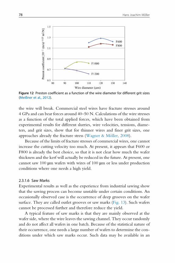
the wire will break. Commercial steel wires have fracture stresses around
4 GPa and can bear forces around 40–50 N. Calculations of the wire stresses
as a function of the total applied forces, which have been obtained from
experimental results for different slurries, wire velocities, tensions, diame-
ters, and grit sizes, show that for thinner wires and finer grit sizes, one
approaches already the fracture stress (Wagner & M€oller, 2008).Because of the limits of fracture stresses of commercial wires, one cannot
increase the cutting velocity too much. At present, it appears that F600 or
F800 is already the best choice, so that it is not clear how much the wafer
thickness and the kerf will actually be reduced in the future. At present, one
cannot saw 100 μm wafers with wires of 100 μm or less under production
conditions where one needs a high yield.
2.3.1.6 Saw MarksExperimental results as well as the experience from industrial sawing show
that the sawing process can become unstable under certain conditions. An
occasionally observed case is the occurrence of deep grooves on the wafer
surface. They are called outlet grooves or saw marks (Fig. 13). Such wafers
cannot be processed further and therefore reduce the yield.
A typical feature of saw marks is that they are mainly observed at the
wafer side, where the wire leaves the sawing channel. They occur randomly
and do not affect all wafers in one batch. Because of the statistical nature of
their occurrence, one needs a large number of wafers to determine the con-
ditions under which saw marks occur. Such data may be available in an
Figure 12 Preston coefficient as a function of the wire diameter for different grit sizes(Meißner et al., 2012).
78 Hans Joachim M€oller
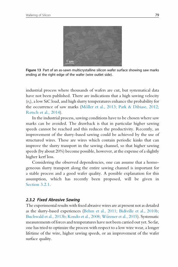
industrial process where thousands of wafers are cut, but systematical data
have not been published. There are indications that a high sawing velocity
(vs), a low SiC load, and high slurry temperatures enhance the probability for
the occurrence of saw marks (M€oller et al., 2013; Park & Dibiase, 2012;
Retsch et al., 2014).
In the industrial process, sawing conditions have to be chosen where saw
marks can be avoided. The drawback is that in particular higher sawing
speeds cannot be reached and this reduces the productivity. Recently, an
improvement of the slurry-based sawing could be achieved by the use of
structured wires. These are wires which contain periodic kinks that can
improve the slurry transport in the sawing channel, so that higher sawing
speeds (by about 20%) become possible, however, at the expense of a slightly
higher kerf loss.
Considering the observed dependencies, one can assume that a homo-
geneous slurry transport along the entire sawing channel is important for
a stable process and a good wafer quality. A possible explanation for this
assumption, which has recently been proposed, will be given in
Section 3.2.1.
2.3.2 Fixed Abrasive SawingThe experimental results with fixed abrasivewires are at present not as detailed
as the slurry-based experiences (Behm et al., 2011; Bidiville et al., 2010b;
Buchwald et al., 2013b; Kondo et al., 2008;W€urzner et al., 2015). Systematic
measurements of forces and temperatures have not been carried out yet. So far,
one has tried to optimize the process with respect to a lowwire wear, a longer
lifetime of the wire, higher sawing speeds, or an improvement of the wafer
surface quality.
Figure 13 Part of an as-sawn multicrystalline silicon wafer surface showing saw marksending at the right edge of the wafer (wire outlet side).
79Wafering of Silicon
Wire breakage is also an important problem because of the high wire
cost. Diamond-coated wires are more prone to wire breakage due to the
protruding particles on the surface. The wire can get stuck in the sawing
channel or during winding up in the spools. One has to find sawing condi-
tions under which that problem can be reduced.
Wire wear is also important because diamond particles can break out,
which reduces the sawing performance. The loss of abrasive particles deter-
mines the number of cycles in the oscillating mode for which a wire can be
used. This situation may become better when improved wires become avail-
able in the future.
Typical sawing conditions are that about 300–800 m of wire is used in
one direction before the wire motion is reversed. The backward movement
is shorter by about a few meters so that in each cycle a fresh wire segment is
added. The deceleration and acceleration phases have to be kept short, but
depend on the machine type. Down to 1.5 s is feasible today, but one can
expect that improved machine types will be constructed in the future when
the technique becomes established. The cutting times of a standard silicon
ingot can be reduced today by a factor of 2 approximately. Another aspect is
the wafer quality which will be discussed next.
2.4 Determination of Wafer PropertiesThe detailed evaluation of the sawing process also requires a closer look at the
wafer surface quality. Moreover, it is possible to draw conclusions from the
wafer surface properties with regard to the cutting process. For the solar cell
process, it is necessary to have wafers with preferable uniform thickness and
low surface damage. The thickness variation of a wafer is thus an important
specification parameter for a wafer. The wafer surface damage can be
described by the roughness and subsurface damage, which consists of micro-
cracksmainly perpendicular to the surface and usually between 2 and 20 μm in
length. This damage has to be removed by etching before solar cell processing.
In addition, the etching should result in a textured surface to improve the opti-
cal reflectivity of the solar cell. Experience shows that the etching process
depends on the surface profile. It requires for instance adjustments if thewafers
are sawn by fixed abrasive wires, because they have a different surface profile.
The microcracks are generated by indenting the abrasive particles. They
extend from the wafer surface into the volume and directly determine the
wafer stability. These cracks depend on the shape, the size and the indenting
force of particles, wire load, and wire speed.
80 Hans Joachim M€oller
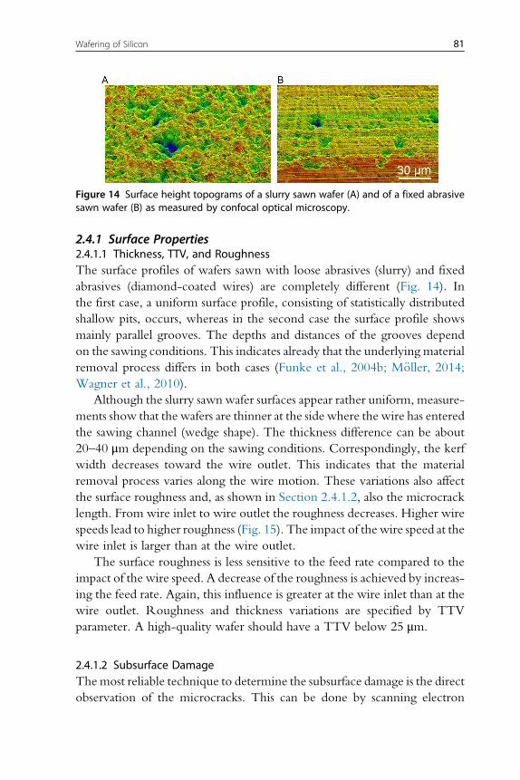
2.4.1 Surface Properties2.4.1.1 Thickness, TTV, and RoughnessThe surface profiles of wafers sawn with loose abrasives (slurry) and fixed
abrasives (diamond-coated wires) are completely different (Fig. 14). In
the first case, a uniform surface profile, consisting of statistically distributed
shallow pits, occurs, whereas in the second case the surface profile shows
mainly parallel grooves. The depths and distances of the grooves depend
on the sawing conditions. This indicates already that the underlying material
removal process differs in both cases (Funke et al., 2004b; M€oller, 2014;Wagner et al., 2010).
Although the slurry sawn wafer surfaces appear rather uniform, measure-
ments show that the wafers are thinner at the side where the wire has entered
the sawing channel (wedge shape). The thickness difference can be about
20–40 μm depending on the sawing conditions. Correspondingly, the kerf
width decreases toward the wire outlet. This indicates that the material
removal process varies along the wire motion. These variations also affect
the surface roughness and, as shown in Section 2.4.1.2, also the microcrack
length. From wire inlet to wire outlet the roughness decreases. Higher wire
speeds lead to higher roughness (Fig. 15). The impact of the wire speed at the
wire inlet is larger than at the wire outlet.
The surface roughness is less sensitive to the feed rate compared to the
impact of the wire speed. A decrease of the roughness is achieved by increas-
ing the feed rate. Again, this influence is greater at the wire inlet than at the
wire outlet. Roughness and thickness variations are specified by TTV
parameter. A high-quality wafer should have a TTV below 25 μm.
2.4.1.2 Subsurface DamageThemost reliable technique to determine the subsurface damage is the direct
observation of the microcracks. This can be done by scanning electron
Figure 14 Surface height topograms of a slurry sawn wafer (A) and of a fixed abrasivesawn wafer (B) as measured by confocal optical microscopy.
81Wafering of Silicon
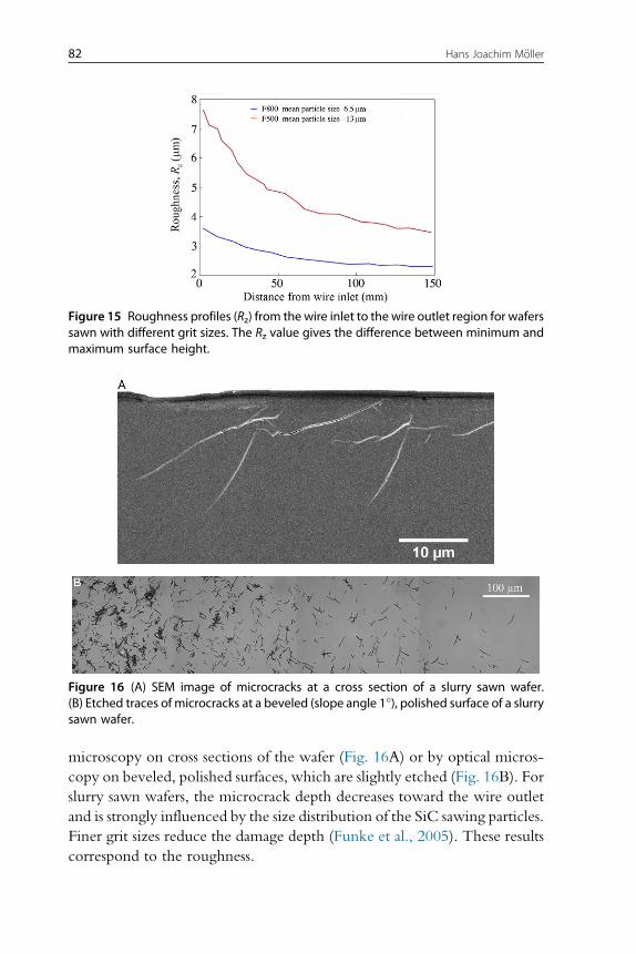
microscopy on cross sections of the wafer (Fig. 16A) or by optical micros-
copy on beveled, polished surfaces, which are slightly etched (Fig. 16B). For
slurry sawn wafers, the microcrack depth decreases toward the wire outlet
and is strongly influenced by the size distribution of the SiC sawing particles.
Finer grit sizes reduce the damage depth (Funke et al., 2005). These results
correspond to the roughness.
Figure 15 Roughness profiles (Rz) from the wire inlet to the wire outlet region for waferssawn with different grit sizes. The Rz value gives the difference between minimum andmaximum surface height.
Figure 16 (A) SEM image of microcracks at a cross section of a slurry sawn wafer.(B) Etched traces of microcracks at a beveled (slope angle 1°), polished surface of a slurrysawn wafer.
82 Hans Joachim M€oller
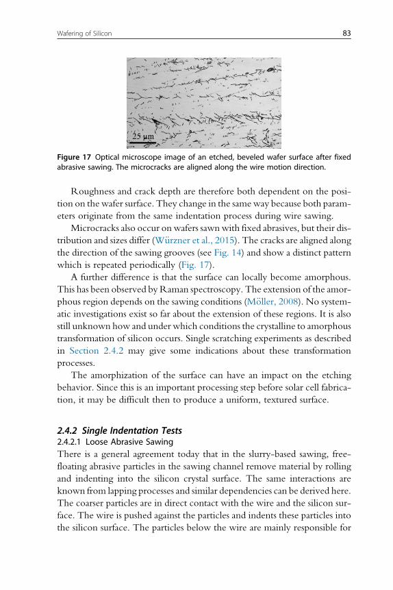
Roughness and crack depth are therefore both dependent on the posi-
tion on the wafer surface. They change in the sameway because both param-
eters originate from the same indentation process during wire sawing.
Microcracks also occur on wafers sawnwith fixed abrasives, but their dis-
tribution and sizes differ (W€urzner et al., 2015). The cracks are aligned alongthe direction of the sawing grooves (see Fig. 14) and show a distinct pattern
which is repeated periodically (Fig. 17).
A further difference is that the surface can locally become amorphous.
This has been observed byRaman spectroscopy. The extension of the amor-
phous region depends on the sawing conditions (M€oller, 2008). No system-
atic investigations exist so far about the extension of these regions. It is also
still unknown how and under which conditions the crystalline to amorphous
transformation of silicon occurs. Single scratching experiments as described
in Section 2.4.2 may give some indications about these transformation
processes.
The amorphization of the surface can have an impact on the etching
behavior. Since this is an important processing step before solar cell fabrica-
tion, it may be difficult then to produce a uniform, textured surface.
2.4.2 Single Indentation Tests2.4.2.1 Loose Abrasive SawingThere is a general agreement today that in the slurry-based sawing, free-
floating abrasive particles in the sawing channel remove material by rolling
and indenting into the silicon crystal surface. The same interactions are
known from lapping processes and similar dependencies can be derived here.
The coarser particles are in direct contact with the wire and the silicon sur-
face. The wire is pushed against the particles and indents these particles into
the silicon surface. The particles below the wire are mainly responsible for
Figure 17 Optical microscope image of an etched, beveled wafer surface after fixedabrasive sawing. The microcracks are aligned along the wire motion direction.
83Wafering of Silicon
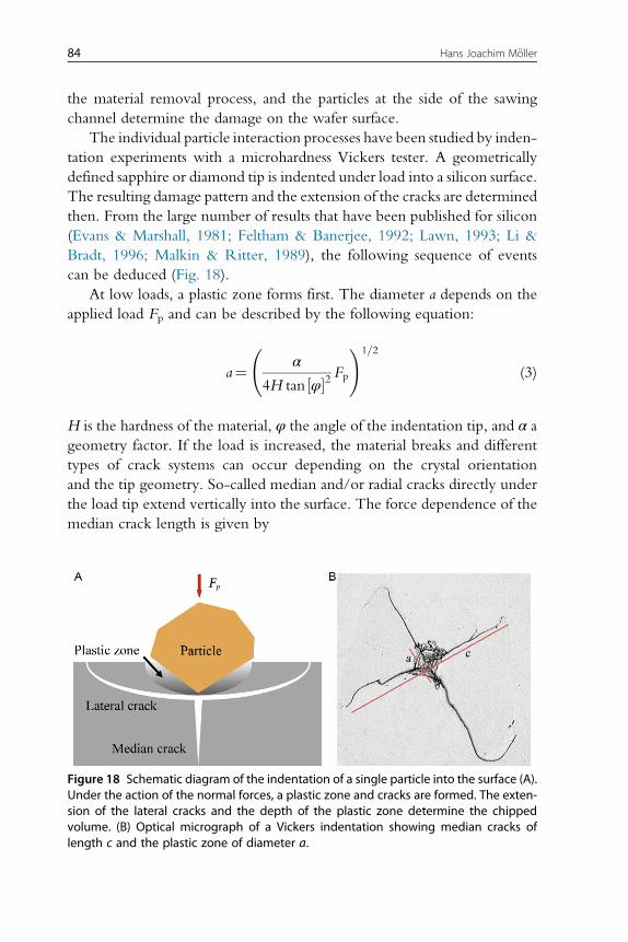
the material removal process, and the particles at the side of the sawing
channel determine the damage on the wafer surface.
The individual particle interaction processes have been studied by inden-
tation experiments with a microhardness Vickers tester. A geometrically
defined sapphire or diamond tip is indented under load into a silicon surface.
The resulting damage pattern and the extension of the cracks are determined
then. From the large number of results that have been published for silicon
(Evans & Marshall, 1981; Feltham & Banerjee, 1992; Lawn, 1993; Li &
Bradt, 1996; Malkin & Ritter, 1989), the following sequence of events
can be deduced (Fig. 18).
At low loads, a plastic zone forms first. The diameter a depends on the
applied load Fp and can be described by the following equation:
a¼ α
4H tan φ½ �2 Fp
!1=2
(3)
H is the hardness of the material, φ the angle of the indentation tip, and α a
geometry factor. If the load is increased, the material breaks and different
types of crack systems can occur depending on the crystal orientation
and the tip geometry. So-called median and/or radial cracks directly under
the load tip extend vertically into the surface. The force dependence of the
median crack length is given by
Figure 18 Schematic diagram of the indentation of a single particle into the surface (A).Under the action of the normal forces, a plastic zone and cracks are formed. The exten-sion of the lateral cracks and the depth of the plastic zone determine the chippedvolume. (B) Optical micrograph of a Vickers indentation showing median cracks oflength c and the plastic zone of diameter a.
84 Hans Joachim M€oller
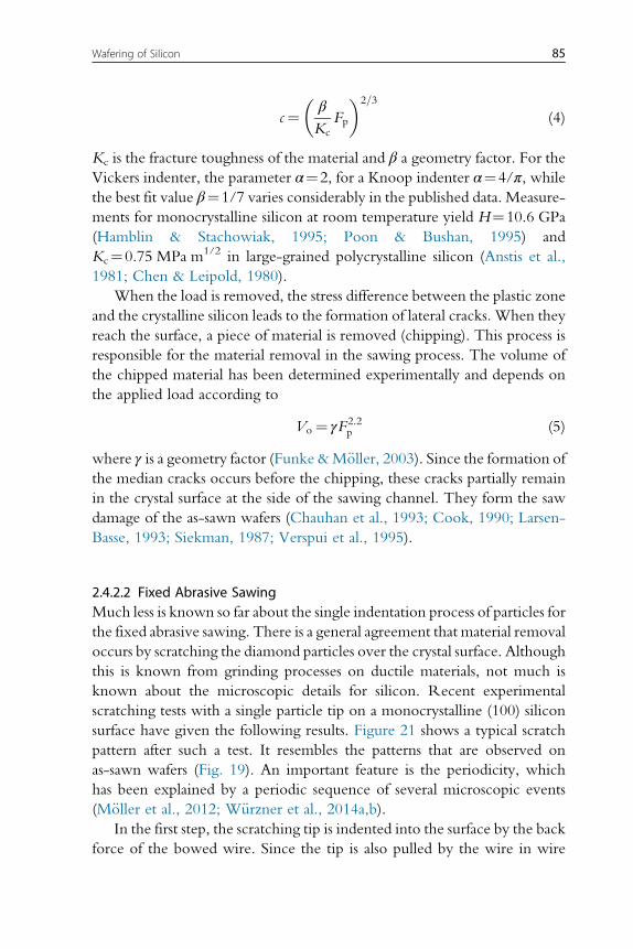
c¼ β
Kc
Fp
� �2=3
(4)
Kc is the fracture toughness of the material and β a geometry factor. For the
Vickers indenter, the parameter α¼2, for a Knoop indenter α¼4/π, whilethe best fit value β¼1/7 varies considerably in the published data. Measure-
ments for monocrystalline silicon at room temperature yield H¼10.6 GPa
(Hamblin & Stachowiak, 1995; Poon & Bushan, 1995) and
Kc¼0.75 MPa m1/2 in large-grained polycrystalline silicon (Anstis et al.,
1981; Chen & Leipold, 1980).
When the load is removed, the stress difference between the plastic zone
and the crystalline silicon leads to the formation of lateral cracks. When they
reach the surface, a piece of material is removed (chipping). This process is
responsible for the material removal in the sawing process. The volume of
the chipped material has been determined experimentally and depends on
the applied load according to
Vo¼ γF2:2p (5)
where γ is a geometry factor (Funke &M€oller, 2003). Since the formation of
the median cracks occurs before the chipping, these cracks partially remain
in the crystal surface at the side of the sawing channel. They form the saw
damage of the as-sawn wafers (Chauhan et al., 1993; Cook, 1990; Larsen-
Basse, 1993; Siekman, 1987; Verspui et al., 1995).
2.4.2.2 Fixed Abrasive SawingMuch less is known so far about the single indentation process of particles for
the fixed abrasive sawing. There is a general agreement that material removal
occurs by scratching the diamond particles over the crystal surface. Although
this is known from grinding processes on ductile materials, not much is
known about the microscopic details for silicon. Recent experimental
scratching tests with a single particle tip on a monocrystalline (100) silicon
surface have given the following results. Figure 21 shows a typical scratch
pattern after such a test. It resembles the patterns that are observed on
as-sawn wafers (Fig. 19). An important feature is the periodicity, which
has been explained by a periodic sequence of several microscopic events
(M€oller et al., 2012; W€urzner et al., 2014a,b).In the first step, the scratching tip is indented into the surface by the back
force of the bowed wire. Since the tip is also pulled by the wire in wire
85Wafering of Silicon
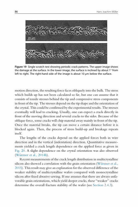
motion direction, the resulting force faces obliquely into the bulk. The stress
which builds up has not been calculated so far, but one can assume that it
consists of tensile stresses behind the tip and compressive stress components
in front of the tip. The stresses depend on the tip shape and the orientation of
the crystal. This could be confirmed by the experimental results. The stresses
eventually will lead to cracking. Usually, one can expect a crack directly in
front of the moving direction and several cracks to the sides. Because of the
oblique force, some cracks will chip material away mainly in front of the tip.
Once the material breaks, the tip can move a certain distance before it is
blocked again. Then, the process of stress build-up and breakage repeats
itself.
The lengths of the cracks depend on the applied forces both in wire
direction and in the vertical (indentation) direction. Quantitative measure-
ments yielded a crack length dependence on the applied force as given in
Fig. 20. A slight dependence on the crystal orientation was also observed
(W€urzner et al., 2014b).Recent measurements of the crack length distribution in multicrystalline
silicon also showed a correlation with the grain orientation (W€urzner et al.,2015). This result may give an explanation for the observed difference of the
weaker stability of multicrystalline wafers compared with monocrystalline
silicon after fixed abrasive sawing. If one assumes that there are always unfa-
vorable grain orientations, which yield deeper cracks, these “weaker” cracks
determine the overall fracture stability of the wafer (see Section 2.4.3).
Figure 19 Single scratch test showing periodic crack patterns. The upper image showsthe damage at the surface. In the lower image, the surface is inclined by about 1° fromleft to right. The right-hand side of the image is about 10 μm below the surface.
86 Hans Joachim M€oller
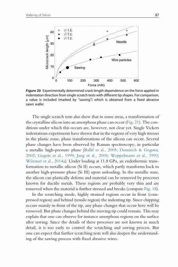
The single scratch tests also show that in some areas, a transformation of
the crystalline silicon into an amorphous phase can occur (Fig. 21). The con-
ditions under which this occurs are, however, not clear yet. Single Vickers
indentations experiments have shown that in the regions of very high stresses
in the plastic zone, phase transformations of the silicon can occur. Several
phase changes have been observed by Raman spectroscopy, in particular
a metallic high-pressure phase (Ballif et al., 2005; Domnich & Gogotsi,
2002; Gogots et al., 1999; Jang et al., 2005; Weppelmann et al., 1993;
W€urzner et al., 2014a). Under loading at 11.8 GPa, an endothermic trans-
formation to metallic silicon (Si II) occurs, which partly transforms back to
another high-pressure phase (Si III) upon unloading. In the metallic state,
the silicon can plastically deform and material can be removed by processes
known for ductile metals. These regions are probably very thin and are
removed when the material is further stressed and breaks (compare Fig. 18).
In the scratching mode, highly strained regions occur in front (com-
pressed region) and behind (tensile region) the indenting tip. Since chipping
occurs mainly in front of the tip, any phase changes that occur here will be
removed. But phase changes behind the moving tip could remain. This may
explain that one can observe for instance amorphous regions on the surface
after sawing. Since the details of these processes are not known in much
detail, it is too early to control the scratching and sawing process. But
one can expect that further scratching tests will also deepen the understand-
ing of the sawing process with fixed abrasive wires.
Figure 20 Experimentally determined crack length dependence on the force applied inindentation direction from single scratch tests with different tip shapes. For comparison,a value is included (marked by “sawing”) which is obtained from a fixed abrasivesawn wafer.
87Wafering of Silicon
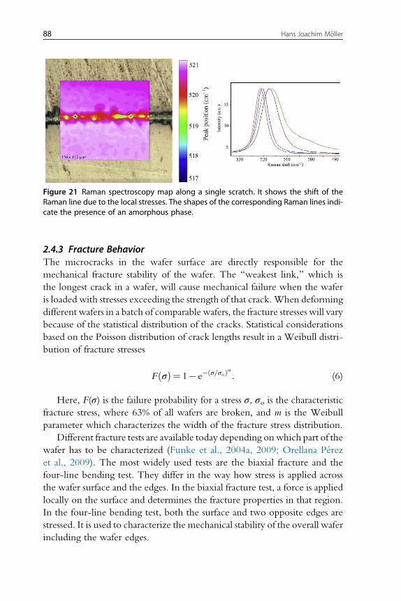
2.4.3 Fracture BehaviorThe microcracks in the wafer surface are directly responsible for the
mechanical fracture stability of the wafer. The “weakest link,” which is
the longest crack in a wafer, will cause mechanical failure when the wafer
is loaded with stresses exceeding the strength of that crack.When deforming
different wafers in a batch of comparable wafers, the fracture stresses will vary
because of the statistical distribution of the cracks. Statistical considerations
based on the Poisson distribution of crack lengths result in a Weibull distri-
bution of fracture stresses
F σð Þ¼ 1� e� σ=σoð Þm : (6)
Here, F(σ) is the failure probability for a stress σ, σo is the characteristicfracture stress, where 63% of all wafers are broken, and m is the Weibull
parameter which characterizes the width of the fracture stress distribution.
Different fracture tests are available today depending onwhich part of the
wafer has to be characterized (Funke et al., 2004a, 2009; Orellana Perez
et al., 2009). The most widely used tests are the biaxial fracture and the
four-line bending test. They differ in the way how stress is applied across
the wafer surface and the edges. In the biaxial fracture test, a force is applied
locally on the surface and determines the fracture properties in that region.
In the four-line bending test, both the surface and two opposite edges are
stressed. It is used to characterize the mechanical stability of the overall wafer
including the wafer edges.
Figure 21 Raman spectroscopy map along a single scratch. It shows the shift of theRaman line due to the local stresses. The shapes of the corresponding Raman lines indi-cate the presence of an amorphous phase.
88 Hans Joachim M€oller
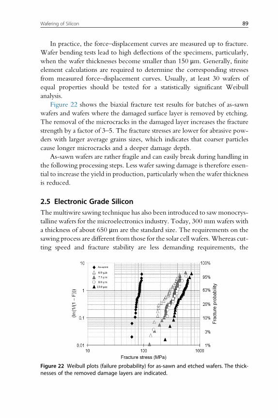
In practice, the force–displacement curves are measured up to fracture.
Wafer bending tests lead to high deflections of the specimens, particularly,
when the wafer thicknesses become smaller than 150 μm. Generally, finite
element calculations are required to determine the corresponding stresses
from measured force–displacement curves. Usually, at least 30 wafers of
equal properties should be tested for a statistically significant Weibull
analysis.
Figure 22 shows the biaxial fracture test results for batches of as-sawn
wafers and wafers where the damaged surface layer is removed by etching.
The removal of the microcracks in the damaged layer increases the fracture
strength by a factor of 3–5. The fracture stresses are lower for abrasive pow-
ders with larger average grains sizes, which indicates that coarser particles
cause longer microcracks and a deeper damage depth.
As-sawn wafers are rather fragile and can easily break during handling in
the following processing steps. Less wafer sawing damage is therefore essen-
tial to increase the yield in production, particularly when the wafer thickness
is reduced.
2.5 Electronic Grade SiliconThe multiwire sawing technique has also been introduced to sawmonocrys-
talline wafers for the microelectronics industry. Today, 300 mmwafers with
a thickness of about 650 μm are the standard size. The requirements on the
sawing process are different from those for the solar cell wafers.Whereas cut-
ting speed and fracture stability are less demanding requirements, the
Figure 22 Weibull plots (failure probability) for as-sawn and etched wafers. The thick-nesses of the removed damage layers are indicated.
89Wafering of Silicon
planarity in the nanometer range over the entire wafer surface is very impor-
tant. Although the following processing steps, grinding, lapping, and
polishing, produce the final surface quality, also the sawing step has to be
very precise. Thickness variations that occur here require higher efforts in
the following steps to remove them and are therefore expensive.
The wafers are cut in the oscillating mode which avoids the wedge shape
of the slurry sawn wafer. The adjustment of the wire speed, tension, and
other parameters enable one already to produce high-quality wafer surfaces.
A problem, however, that remains is when the wires first cut into the crystal.
It has been observed that the wafers often show a shallow bump of a few
micrometers at the rim of the surface which has to be removed afterward.
It is assumed that the wires move sideways before they cut into the material
and straighten out afterward during cutting. The reason for the sideward
motion is not quite clear but may have to do with some irregularities on
the crystal surface. In general, when cutting monocrystalline wafers, the pre-
cise control of the wire motion through the crystal is the most demanding
requirement.
3. BASIC SAWING MECHANISMS
Slurry-based sawing has been optimized for many years now by prac-
tical experience. Further improvements are possible but are more like a fine-
tuning of the process. This requires, however, a good understanding of the
basic mechanisms. Great progress has been made here over the years
(Bhagavat et al., 2000; Buijs & Korpel-van Houten, 1993c; Ferris &
Chandrasekar, 1994; Funke et al., 2009; Li et al., 1998; M€oller, 2004;Wei & Kao, 2000; Yang & Kao, 1999, 2000). The description of the loose
abrasive process is based on the individual process of the interactions of a
single particle with the crystal surface and the resulting microfracture
processes. The main ideas will be outlined in the following.
3.1 Slurry-Based SawingUnder normal sawing conditions, the space between the wire and the crystal
surface is filled with fluid and abrasive particles (slurry). Experimental inves-
tigations with a high-speed camera indicate that the wire is in direct contact
with the largest particles. They determine the distance between the wire and
crystal surface. The smaller particles are floating freely (Fig. 23). SiC particles
are facetted and contain sharp edges and tips, which can exert very high local
pressures. The microscopic material removal process is explained by the
90 Hans Joachim M€oller

interaction of rolling SiC particles that are randomly indented into the crystal
surface until small silicon pieces are chipped away. This “rolling–indenting
grain” model forms the physical basis of the wire sawing process. The same
mechanism also occurs in lapping brittle material surfaces with loose abrasive
particles (Buijs & Korpel-van Houten, 1993a,b; Su et al., 1996).
It is assumed that only the larger particles which are in direct contact par-
ticipate in the material removal process. During sawing, the crystal is pushed
against the wires with a constant forward (feed) velocity. With increasing
velocity, the total force Ftot on the wire increases and more and more par-
ticles are indented. Since the wire is elastic, it will bow under the force like a
string. The resulting wire curvature adjusts to achieve an overall constant
feed velocity.
One has to consider here that the forces vary below the wire, depending
on the local conditions in the sawing channel. Considering the cross-
sectional view, the resulting force perpendicular to the wire surface which
pushes the particles into the surface also varies along the contact area. The
forces are maximal directly below the wire and decrease toward the side faces
(Fig. 24). The cutting process at the wafer side and the applied force there is
important because it determines the final surface quality of the sliced wafers.
Furthermore, the fast-moving slurry builds up a hydrodynamic pressure,
which may exert additional force on the wire. The hydrodynamic pressure
also decreases toward the sides of the channel because it is zero at the free
slurry surface. Particles in the channel will be pushed sideways because of
a pressure difference and eventually be removed from the sawing channel
when they reach the free slurry surface. Since the pressure difference
depends on the particle size, one can expect a rearrangement of the particle
size distribution by the removal of larger particles from the sawing channel
below the wire. In fact, several results have been reported, which show that
Figure 23 Schematic diagram of the sawing channel. It shows the main forces that areassumed in the model.
91Wafering of Silicon
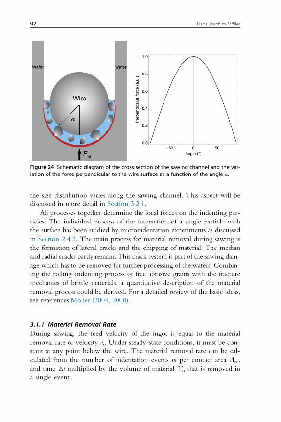
the size distribution varies along the sawing channel. This aspect will be
discussed in more detail in Section 3.2.1.
All processes together determine the local forces on the indenting par-
ticles. The individual process of the interaction of a single particle with
the surface has been studied by microindentation experiments as discussed
in Section 2.4.2. The main process for material removal during sawing is
the formation of lateral cracks and the chipping of material. The median
and radial cracks partly remain. This crack system is part of the sawing dam-
age which has to be removed for further processing of the wafers. Combin-
ing the rolling–indenting process of free abrasive grains with the fracture
mechanics of brittle materials, a quantitative description of the material
removal process could be derived. For a detailed review of the basic ideas,
see references M€oller (2004, 2008).
3.1.1 Material Removal RateDuring sawing, the feed velocity of the ingot is equal to the material
removal rate or velocity vs. Under steady-state conditions, it must be con-
stant at any point below the wire. The material removal rate can be cal-
culated from the number of indentation events m per contact area Atot
and time △t multiplied by the volume of material Vo that is removed in
a single event
Figure 24 Schematic diagram of the cross section of the sawing channel and the var-iation of the force perpendicular to the wire surface as a function of the angle α.
92 Hans Joachim M€oller
vs ¼ mVo
AtotΔt: (7)
The material volume Vo that can be removed in a single event is deter-
mined by the extension of the lateral cracks below the indentation of a single
grain (Fig. 18). It depends on the applied normal force Fp on the particle
according to Eq. (5).
The velocity profile of the laminar flow in the slurry leads to a rotation of
the particles. If a rolling grain makes one indentation per cycle, the average
time interval for a single indentation event is given by△t¼2dp/v, where v is
the wire velocity and dp the particle diameter which is determined by the
largest particles in the size distribution.
The experimental results show that wire distance, particle size distribu-
tion, the temperature, and other parameters vary along the sawing channel.
Therefore, it is necessary to consider the local situation. Each wire segment
exerts a force Fn on the particles, which depends on the local curvature and
the wire tension. For a rigid wire segment, the resulting average force on a
single particle Fp is given by Fp ¼Fn=m, where m is the number of all the
particles in contact under the segment. For a short segment of length dx,
one can write
Fp¼ @Fn=@x
@m=@x: (8)
Combining the equations yields for the local sawing rate, the fundamen-
tal relationship which forms the basis for the following theoretical
description:
vs ¼ vso∗ v@m=@x
dprw
@Fn=@x
@m=@x
� �n
, (9)
where the prefactor vso∗ summarizes material and geometry parameters. The
contact area below the wire has been expressed by Atot¼πrwdx here, with
the wire radius rw. The remaining problem that has to be solved is to deter-
mine the numberm of indenting grains in the slurry and the average force Fnper wire segment dx.
The number m of particles in contact and the average force Fn are cal-
culated from the grain size distribution. Commercial virgin SiC particle sizes
can be described rather well by a Gaussian distribution. In general, the size
distribution will differ from this form, particularly when slurry is transported
along the sawing channel and particles are lost or break. It is useful therefore
93Wafering of Silicon
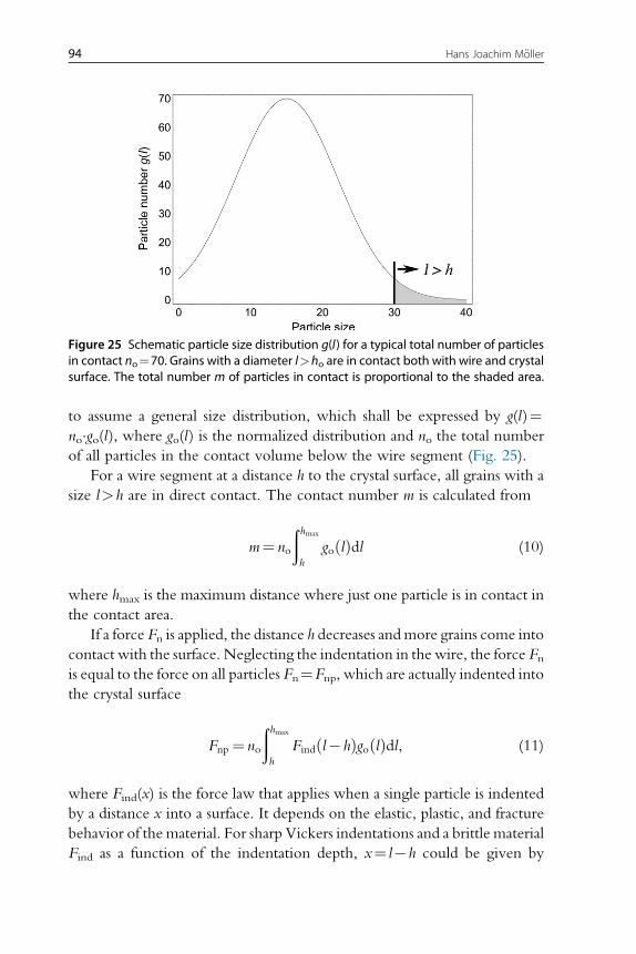
to assume a general size distribution, which shall be expressed by g(l)¼no�go(l), where go(l) is the normalized distribution and no the total number
of all particles in the contact volume below the wire segment (Fig. 25).
For a wire segment at a distance h to the crystal surface, all grains with a
size l>h are in direct contact. The contact number m is calculated from
m¼ no
ðhmax
h
go lð Þdl (10)
where hmax is the maximum distance where just one particle is in contact in
the contact area.
If a force Fn is applied, the distance h decreases andmore grains come into
contact with the surface. Neglecting the indentation in the wire, the force Fnis equal to the force on all particles Fn¼Fnp, which are actually indented into
the crystal surface
Fnp¼ no
ðhmax
h
Find l�hð Þgo lð Þdl, (11)
where Find(x) is the force law that applies when a single particle is indented
by a distance x into a surface. It depends on the elastic, plastic, and fracture
behavior of the material. For sharp Vickers indentations and a brittle material
Find as a function of the indentation depth, x¼ l�h could be given by
Figure 25 Schematic particle size distribution g(l) for a typical total number of particlesin contact no¼70. Grains with a diameter l>ho are in contact both with wire and crystalsurface. The total number m of particles in contact is proportional to the shaded area.
94 Hans Joachim M€oller
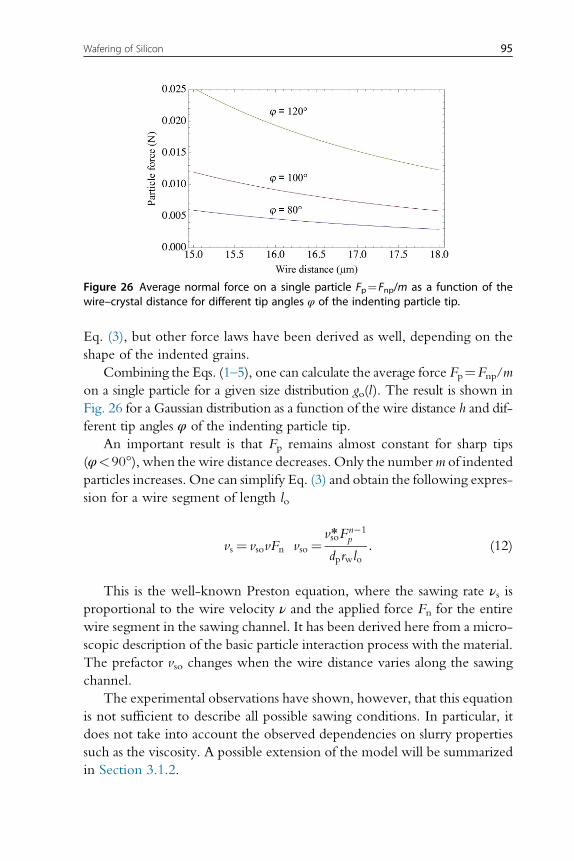
Eq. (3), but other force laws have been derived as well, depending on the
shape of the indented grains.
Combining the Eqs. (1–5), one can calculate the average force Fp¼Fnp/m
on a single particle for a given size distribution go(l). The result is shown in
Fig. 26 for a Gaussian distribution as a function of the wire distance h and dif-
ferent tip angles φ of the indenting particle tip.
An important result is that Fp remains almost constant for sharp tips
(φ<90°), when the wire distance decreases. Only the numberm of indented
particles increases. One can simplify Eq. (3) and obtain the following expres-
sion for a wire segment of length lo
vs ¼ vsovFn vso¼vso∗Fn�1
p
dprwlo: (12)
This is the well-known Preston equation, where the sawing rate νs isproportional to the wire velocity ν and the applied force Fn for the entire
wire segment in the sawing channel. It has been derived here from a micro-
scopic description of the basic particle interaction process with the material.
The prefactor vso changes when the wire distance varies along the sawing
channel.
The experimental observations have shown, however, that this equation
is not sufficient to describe all possible sawing conditions. In particular, it
does not take into account the observed dependencies on slurry properties
such as the viscosity. A possible extension of the model will be summarized
in Section 3.1.2.
Figure 26 Average normal force on a single particle Fp¼Fnp/m as a function of thewire–crystal distance for different tip angles φ of the indenting particle tip.
95Wafering of Silicon
3.1.2 Elastohydrodynamic Behavior of Slurry and WireTaking into account slurry properties, one has to consider the hydrodynamic
behavior of the slurry in the sawing channel (M€oller, 2004; M€oller et al.,2013). The slurry consists of the fluid and a high volume concentration
of particles. In general, one has to describe this as a two-phase flow problem.
In the following, the simplification is made that one has a single-phase sys-
tem, where only the viscosity is changed by the addition of the abrasive
powder. The viscosity changes can be described by Eq. (2). Because of
the narrow sawing channel, one can assume a laminar flow of the slurry.
A similar situation occurs in lubrication and polishing processes, where many
fundamental aspects have been derived from experimental and theoretical
results (Chauhan et al., 1993; Cook, 1990; Kasai & Doy, 1992; Larsen-
Basse, 1993; Siekman, 1987; Su et al., 1996; Verspui et al., 1995). An impor-
tant aspect is that a hydrodynamic pressure can build up in the slurry and, if
high enough, deform the wire elastically in response to the pressure (Fig. 24).
Some consequences can be derived from a one-dimensional treatment of the
hydrodynamic slurry transport below a flexible wire. The starting point to
describe the slurry flow directly below the wire is the Reynolds equation
@p
@x¼ 6vη
h�ho
h3, (13)
where x is the coordinate along the wire, h(x) the distance between wire and
crystal surface, v the wire velocity, η the slurry viscosity, and p(x) the hydro-dynamic slurry pressure. ho is a constant which has to be derived from
boundary conditions. The hydrodynamic pressure in the slurry exerts forces
on the wire, which will deform elastically then.
Like for a pulled string, the local curvature of the wire determines the
resulting backward force Fn normal to the wire. If we describe the shape
of the bowed wire by the vertical displacement y(x), the force (per length)
@Fn/@x and the corresponding pressure p are related to the (negative)
curvature, which is the second derivative of y, by
@Fn
@x¼�Ty00 p¼ 1
πreff
@Fn
@x¼� T
πreffy00, (14)
where T is the tensile force along the wire (Fig. 24). In the one-dimensional
treatment, the pressure below the wire is only constant over an effective seg-
ment length reff. If one expresses the width of the slurry transport channel by
h(x)¼y(x)�yo(x), where yo(x) describes the shape of the crystal surface, one
obtains
96 Hans Joachim M€oller
p¼ po + ph ph ¼� T
πreff
@2h
@x2po¼ T
πreff
@Fn
@x, (15)
where the surface curvature has been expressed by a constant pressure po and
a constant normal force Fno. Experimental investigations of the shape of the
surface during cutting have shown that it is slightly curved and deviates only
very little from a circular shape at least over longer segments of the cutting
length. In equilibrium between wire and slurry, the pressures in Eqs. (13)
and (15) have to be equal. Since po is assumed constant over the segment
length, the derivative is zero and one obtains by inserting
@3h
@x3+6πvηreff
T
h�ho
h3¼ 0: (16)
This equation is the basis for the investigation of the hydrodynamic slurry
behavior. It has no analytical solution but previous numerical solutions show
that the wire distance h differs only slightly from ho, so that one can approx-
imate the equation quite well by (M€oller et al., 2013)
@3h
@x3+6πvηreffTh3o
h�hoð Þ¼ 0: (17)
This equation has the following analytical solution:
h¼ ho + c1e�a1=3x + c2e
a1=3x=2cosffiffiffi3
pa1=3x=2
h i+ c3e
a1=3x=2sinffiffiffi3
pa1=3x=2
h i,
(18)
where
a¼ 6πvηreffTh3o
: (19)
The integration constants c1, c2, and c3 are determined from boundary
conditions. Appropriate boundary conditions are the pressure at wire inlet
p(0)¼pa and outlet p(lo)¼0, and the wire distance at the outlet h(lo)¼ho.
The total pressure can be derived from Eq. (15) if po is known. If ph is
small compared to po, the pressure p and po are approximately equal (p�po).
In this case, the pressure is determined by the local force Fno resulting from
the ingot feed and wire bow. It is equal to the force Fnp, which has been
calculated from the total force on all indented particles by Eq. (8).
A significant hydrodynamic pressure will push the wire away from the
ingot surface. This reduces the sawing rate since the force on a single particle
97Wafering of Silicon
is reduced and fewer particles are in contact (see Eq. 6). Numerical results
show that this is particularly the case in the exit region of the sawing channel,
when ph becomes large. For ph>0, one obtains in this case for the force per
wire segment length
@Fhnp
@x¼ @Fnp
@x� ph (20)
where ph is given in Eq. (15). When ph is negative, the hydrodynamic pres-
sure p has to be neglected because p<po then. This means it has no effect on
the local distance of the wire, which is entirely determined by the particles in
contact then.
3.1.3 Numerical Simulation of the Sawing ProcessThe pressure can be calculated from equations (12 and 15–17) together with
the boundary conditions for a wide range of sawing parameters. Typical
values for wire sawing are the following: ingot cutting length lo¼156 mm,
wire speed v¼15 m/s, viscosity η¼300 cP, wire tension T¼25 N, and
slurry inlet temperature T¼22 °C. The entry pressure of the slurry arises
from the accumulation of fluid at the wire inlet and has been estimated to
be about pa<0.01 MPa (Bhagavat et al., 2000). Figure 27 shows the pressure
along the sawing channel position for two feed velocities vs. In the calcula-
tions, it has been taken into account that the viscosity and the size distribu-
tion change along the sawing channel because of the temperature increase,
the accumulation of silicon and metal debris in the slurry, and the loss of
larger particles, as has been observed experimentally.
Apart from the entry region, the pressure decreases slightly first due
to the loss of larger particles and the reduction of the distance between
wire and crystal surface. The hydrodynamic pressure is too small here to
reduce the forces on the interaction particles, which are exerted by the
bowed wire.
A different situation occurs near the exit region of the sawing channel.
A typical feature is a pressure increase before it drops to zero (for
vs¼0.3 mm/min in Fig. 27). In this case, the hydrodynamic pressure
exerts higher forces on the wire and thus reduces the force on the particles
which are in direct contact and determine the material removal. The
force reduction can become so severe that no material can be removed
anymore. Furthermore, negative pressure values occur before the wire exit
(channel positions >0.9) when the sawing velocity is increased (for
98 Hans Joachim M€oller
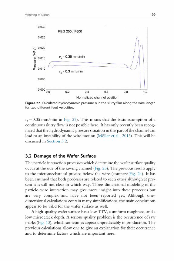
vs¼0.35 mm/min in Fig. 27). This means that the basic assumption of a
continuous slurry flow is not possible here. It has only recently been recog-
nized that the hydrodynamic pressure situation in this part of the channel can
lead to an instability of the wire motion (M€oller et al., 2013). This will bediscussed in Section 3.2.
3.2 Damage of the Wafer SurfaceThe particle interaction processes which determine the wafer surface quality
occur at the side of the sawing channel (Fig. 23). The previous results apply
to the micromechanical process below the wire (compare Fig. 24). It has
been assumed that both processes are related to each other although at pre-
sent it is still not clear in which way. Three-dimensional modeling of the
particle–wire interaction may give more insight into these processes but
are very complex and have not been reported yet. Although one-
dimensional calculations contain many simplifications, the main conclusions
appear to be valid for the wafer surface as well.
A high-quality wafer surface has a low TTV, a uniform roughness, and a
low microcrack depth. A serious quality problem is the occurrence of saw
marks (Fig. 13), which sometimes appear unpredictably in production. The
previous calculations allow one to give an explanation for their occurrence
and to determine factors which are important here.
Figure 27 Calculated hydrodynamic pressure p in the slurry film along the wire lengthfor two different feed velocities.
99Wafering of Silicon
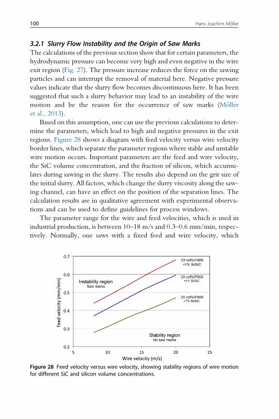
3.2.1 Slurry Flow Instability and the Origin of Saw MarksThe calculations of the previous section show that for certain parameters, the
hydrodynamic pressure can become very high and even negative in the wire
exit region (Fig. 27). The pressure increase reduces the force on the sawing
particles and can interrupt the removal of material here. Negative pressure
values indicate that the slurry flow becomes discontinuous here. It has been
suggested that such a slurry behavior may lead to an instability of the wire
motion and be the reason for the occurrence of saw marks (M€olleret al., 2013).
Based on this assumption, one can use the previous calculations to deter-
mine the parameters, which lead to high and negative pressures in the exit
regions. Figure 28 shows a diagram with feed velocity versus wire velocity
border lines, which separate the parameter regions where stable and unstable
wire motion occurs. Important parameters are the feed and wire velocity,
the SiC volume concentration, and the fraction of silicon, which accumu-
lates during sawing in the slurry. The results also depend on the grit size of
the initial slurry. All factors, which change the slurry viscosity along the saw-
ing channel, can have an effect on the position of the separation lines. The
calculation results are in qualitative agreement with experimental observa-
tions and can be used to define guidelines for process windows.
The parameter range for the wire and feed velocities, which is used in
industrial production, is between 10–18 m/s and 0.3–0.6 mm/min, respec-
tively. Normally, one saws with a fixed feed and wire velocity, which
Figure 28 Feed velocity versus wire velocity, showing stability regions of wire motionfor different SiC and silicon volume concentrations.
100 Hans Joachim M€oller
determines a point in the diagram. Only values below the corresponding
border line are in the stability region. From the industrial perspective of high
productivity and low cost, one will choose a large sawing rate, a small wire
velocity, and a small SiC concentration. One can see from the diagram that
these are conflicting requirements, which limit suitable sets of parameters.
If one chooses parameters close to the border line, small changes in the
sawing parameters can easily lead to a shift from the stable to the unstable
regime. It is therefore necessary to control the specifications of parameters
such as the SiC load, the silicon concentration, or the grit size distribution
quite tightly.
3.2.2 Roughness and Subsurface DamageSawmark-free wafers are a prerequisite for further processing. The quality of
these wafers is then specified by other parameters. The commercially impor-
tant parameter is the TTV of the wafers. It is basically determined by the
difference in thickness and the roughness values at the wire inlet and outlet
side. Good wafers have a TTV<25 μm for wafers with a thickness of
180 μm. If saw marks occur, the TTV can increase up to 60 μm because
of the additional grooves. It is assumed that a strong increase of the TTV
and the occurrence of saw marks are related to the same process, namely
the instability of wire motion near the exit region of the sawing channel
as described in the previous section.
If one saws with parameters in the stability region, the TTV correlates
mainly with the roughness. The dependence of the roughness on feed
and wire velocity and other factors has been investigated experimentally
quite well (see Section 2.4.1). Considering the micromechanical particle–
crystal interaction model, the roughness and the microcrack depth depend
on the forces acting on each particle. Reduced forces will decrease both
roughness and microcrack depth. For instance, smaller grit sizes lead to
smaller forces and a reduced roughness. The observed decrease of the rough-
ness can be explained by the loss of larger particles along the sawing channel
(see Fig. 15).
The roughness also correlates with the microcrack depthwhich is impor-
tant because it mainly determines the fracture behavior of a wafer. There-
fore, sawing conditions which change the overall forces in the process also
have an impact on the wafer stability. The previous numerical calculations
are in good agreement with the observed roughness and microcrack results
and can be used to predict which parameters are significant here (M€olleret al., 2013; Retsch et al., 2014).
101Wafering of Silicon
4. ALTERNATIVE WAFERING TECHNOLOGIES
Many attempts have been carried out to develop alternative
“kerf-less” technologies, which avoid the inherent drawback of the sawing
process, that valuable silicon and supply materials are wasted. Although mul-
tiwire sawing is still a developing wafering technology, there are probably
limitations when wafers with a thickness below 100 μm shall be produced
in the future. Over the past decades, over 20 variants of kerf-less wafering
have been proposed but few have demonstrated a lasting potential to be
competitive in cost and quality (Henley, 2010).
The most direct route is the production of wafers directly from a silicon
melt. The most advanced techniques are the “edge-defined film-fed growth”
technique (Wald, 1981) and the “string ribbon” method (Ciszek, 1981),
which have reached the industrial production level. Less successful were
the “ribbon growth on substrate” method (Lange & Schwirtlich, 1990) and
the Direct Wafer™ technology (Henley et al., 2008b). All liquid-phase
approaches have shown great difficulty in achieving good absorber yield
and quality for standard wafers much below 200 μm. At the same time, the
wire saw process has undergone impressive evolutionary improvements in
the important areas of yield, quality, kerf loss, productivity, and thickness
reduction. As a result, the “kerf-less” material efficiency advantage becomes
moot if the next-generation wire saw processes yield stronger high-efficiency
120–150-μm wafers. This is why these liquid-phase wafering methods have
either been terminated in commercial production or have never started.
Kerf-less technologies, which can overcome the quality problem, start
from solid monocrystalline silicon. The basic principle is to separate many
thin wafers consecutively from a high-quality silicon monocrystal. Several
technologies have emerged, following different approaches: induced cleav-
ing (Baer, 2009; Brailove et al., 2010; Dross et al., 2007; Fujisaka et al., 2011;
Henley et al., 2008a, 2009a,b; Mueller et al., 2003; Nasch et al., 2004), layer
transfer (Bergmann et al., 2002; Petermann et al., 2012), and macropore
reorganization (Depauw et al., 2009, 2010, 2011; Ghannam et al., 2011;
Mizushima et al., 2000; Reuter et al., 2008; Van Nieuwenhuysen et al.,
2012). In the following, the approaches will be described in more detail.
4.1 Cleavage TechnologiesThe most advanced cleavage process uses ion implantation to induce cleav-
ing. First, a high-energy proton beam (or other ions) is directed on the top
102 Hans Joachim M€oller
surface of a Cz silicon ingot. The protons are implanted in a thin layer at a
controlled depth under the surface of the silicon. The proton beam has both
high current and high energy (2–4 MeV). This supplies a high heat load into
the silicon crystal which can reach many tens or even hundreds of kilowatts
and has to be removed by cooling the bricks efficiently. The silicon temper-
ature is a critical part of the process because it can deteriorate the material
quality. After the implant step, the silicon is induced to fracture, or cleave,
in a highly controlled manner, along the cleavage plane defined by the
implanted ions. A single wafer of silicon is released and the process is
repeated on the newly exposed surface of the brick. The use of cleaving,
rather than sawing, eliminates the waste due to kerf.
A light ion implant avoids damaging the bulk silicon while the
low-energy (threshold) cleave process creates only surfaces with low defect
density. Both factors contribute to maintain the high lifetime of the silicon
crystal and high mechanical strength. Bulk lifetimes up to 0.5 ms have been
reported. Roughness of the cleaved wafers is generally less than 1 μm. The
process has also been verified to be capable of repeatedly detaching films
from an ingot without surface preparation between successive detachments.
The films continue to have repeatable roughness and TTV (<1–2%) with-
out any interim polishing or other surface modification steps. Such a wafer-
ing process (Direct Film Transfer) has been developed by the US company
Silicon Genesis. Although it has not yet reached the industrial production
stage, the technique appears to have some potential for an alternative wafer-
ing method (Fujisaka et al., 2011; Henley et al., 2008a, 2009a,b; Mueller
et al., 2003; Nasch et al., 2004; Petermann et al., 2012).
Other cleaving methods use high thermoelastic stresses over the surface.
This can be achieved by depositing a thin polymer- or metal layer on the
surface of a Cz crystal and applying a strong temperature gradient. If the stress
exceeds the required fracture strength, a thin silicon layer can be cleaved
from the brick with high yield. Generally, one has to initiate the crack at
the side of the crystal for instance by laser scribing. After cleavage, the depos-
ited layer is removed again.
4.2 Layer Transfer TechnologiesLift-off techniques have been developed for the microelectronic device
technology. They have the potential to yield thin layers between 10 and
60 μm. The basic principle is the following. A high-quality thin silicon film
is grown on a sacrificial layer, which can be separated and transferred to a
103Wafering of Silicon
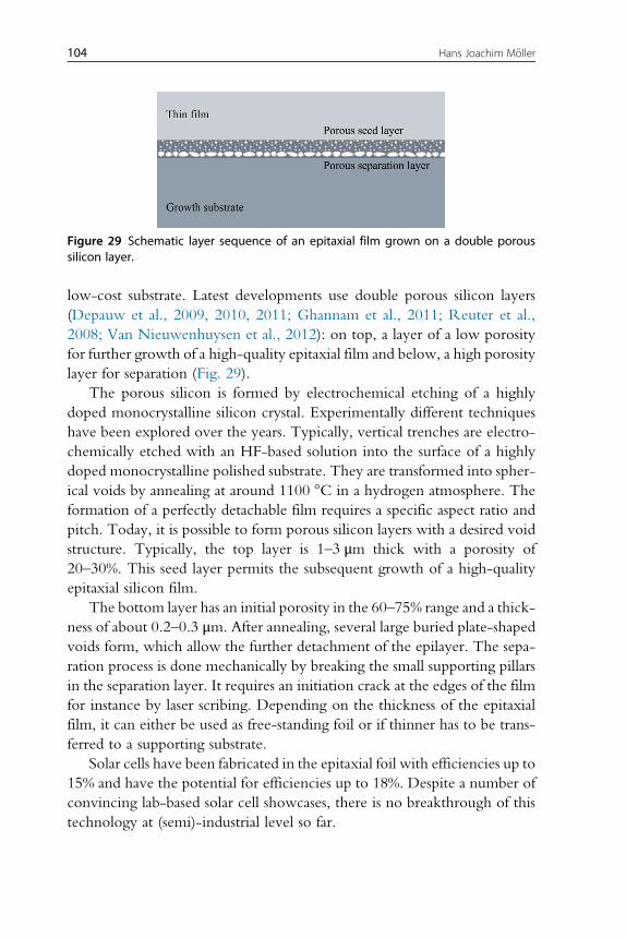
low-cost substrate. Latest developments use double porous silicon layers
(Depauw et al., 2009, 2010, 2011; Ghannam et al., 2011; Reuter et al.,
2008; Van Nieuwenhuysen et al., 2012): on top, a layer of a low porosity
for further growth of a high-quality epitaxial film and below, a high porosity
layer for separation (Fig. 29).
The porous silicon is formed by electrochemical etching of a highly
doped monocrystalline silicon crystal. Experimentally different techniques
have been explored over the years. Typically, vertical trenches are electro-
chemically etched with an HF-based solution into the surface of a highly
doped monocrystalline polished substrate. They are transformed into spher-
ical voids by annealing at around 1100 °C in a hydrogen atmosphere. The
formation of a perfectly detachable film requires a specific aspect ratio and
pitch. Today, it is possible to form porous silicon layers with a desired void
structure. Typically, the top layer is 1–3 μm thick with a porosity of
20–30%. This seed layer permits the subsequent growth of a high-quality
epitaxial silicon film.
The bottom layer has an initial porosity in the 60–75% range and a thick-
ness of about 0.2–0.3 μm. After annealing, several large buried plate-shaped
voids form, which allow the further detachment of the epilayer. The sepa-
ration process is done mechanically by breaking the small supporting pillars
in the separation layer. It requires an initiation crack at the edges of the film
for instance by laser scribing. Depending on the thickness of the epitaxial
film, it can either be used as free-standing foil or if thinner has to be trans-
ferred to a supporting substrate.
Solar cells have been fabricated in the epitaxial foil with efficiencies up to
15% and have the potential for efficiencies up to 18%. Despite a number of
convincing lab-based solar cell showcases, there is no breakthrough of this
technology at (semi)-industrial level so far.
Figure 29 Schematic layer sequence of an epitaxial film grown on a double poroussilicon layer.
104 Hans Joachim M€oller
REFERENCESAnspach, O., Schulze, F.-W., 2007. Glycol to water-based slurry, investigation on the wire
sawing process. In: Proceedings of the 22nd EU PVSEC (WIP, M€unchen, 2007), p. 952.Anstis, G.R., Chantikul, P., Lawn, B.R., Marshall, D.B., 1981. A critical evaluation of
indentation techniques for measuring fracture toughness. J. Am. Ceram. Soc. 64, 533.Aoyama, T., Kondo, Y., Asai, H., Takato, H., Sakata, I., 2009. Fabrication of single-
crystalline silicon solar cells using wafers sliced by a diamond wire saw.In: Proceedings of the 25th European PVSEC, p. 2429.
Assi, F., 2013. Industrial diamond wire sawing. In: Freiberger Sawing Symposium (Freiberg,2013).
Baer, S.C., 2009. Patent No. US 2009/0056513 A1.Ballif, C., Gasser, P., Buerki, G., Michler, J., 2005. In situ micro-Raman compression. Phys.
Status Solidi A 202, 2858.Behm, T., F€utterer, W., Funke, C., Kaminski, S., M€oller, H.J., Rietzschel, R., Wagner, T.,
2011. Challenges of the wire saw wafering process. Photovolt. Int. 11, 38.Bergmann, R.B., Berge, C., Rinke, T.J., Schmidt, J., Werner, J.H., 2002. Advances in
monocrystalline Si thin film solar cells by layer transfer. Sol. Energy Mater. Sol. Cells74, 213.
Bhagavat, M., Prasad, V., Kao, I., 2000. Elastic hydrodynamic interaction in the free abrasivewafer slicing using a wire saw. J. Tribol. 122, 394.
Bidiville, A., Wasmer, K., Kraft, R., Ballif, C., 2009. Diamond wire-sawn silicon wafers—from the lab to the cell production. In: Proceedings of the 24th European PVSEC,p. 1400.
Bidiville, A., Wasmer, K., Michler, J., Nasch, P.M., Van der Meer, M., Ballif, C., 2010a.Mechanism of sawing and impact on wafer properties. Prog. Photovolt. Res. Appl.18, 563.
Bidiville, A., Heiber, J., Wasmer, K., Habegger, S., Assi, F., 2010b. Diamond wire wafering:wafer morphology in comparison to slurry sawn wafers. In: Proceedings of the 25thEuropean PVSEC (WIP, M€unchen, 2010), p. 1673.
Brailove, A., Kang, S., Fujisaka, A., Henley, F., 2010. First demonstration of high volumemanufacturing of kerf-free polymax wafers. In: 25th European PVSEC (WIP,M€unchen,2010), p. 1613.
Buchwald, R., Fr€ohlich, K., W€urzner, S., Lehmann, T., Sunder, K., M€oller, H.J., 2013a.Sub-surface damage of silicon wafers sawn with diamond-coated wire.In: Proceedings of the 28th EU PVSEC (Paris, 2013), p. 1502.
Buchwald, R., Fr€ohlich, K., W€urzner, S., Lehmann, T., Sunder, K., M€oller, H.J., 2013b.Analysis of the sub-surface damage of mc- and cz-Si wafers sawn with diamond-platedwire. Energy Procedia 38, 901.
Buchwald, R., W€urzner, S., Fr€ohlich, K., Fuchs, M., Retsch, S., Lehmann, T., M€oller, H.J.,2014. Analysis of the topography and the sub-surface damage of Cz- and mc-siliconwafers sawn with diamond wire. In: Proceedings of the 40th IEEE Conference(Denver 2014), p. 654.
Buijs, M., Korpel-van Houten, K., 1993a. A model for lapping of glass. J. Mater. Sci.28, 3014–3020 (Chapman & Hill).
Buijs, M., Korpel-van Houten, K., 1993b. Three-body abrasion of brittle materials as studiedby lapping. Wear 166, 237.
Buijs, M., Korpel-van Houten, K., 1993c. Micromechanics of material removal mechanismsfrom brittle surfaces. J. Mater. Sci. 28, 3014.
Bye, J.-I., Jensen, S.A., Aalen, F., Rohr, C., Nielsen, Ø., Gaumann, B., Hodsden, J.,Lindemann, K., 2009. Silicon slicing with diamond wire for commercial productionof PV wafers. In: Proceedings of the 24th European PVSEC, p. 1269.
105Wafering of Silicon
Chauhan, R., Ahn, Y., Chandrasekar, S., Farris, T., 1993. Role of indentation fracture in freeabrasive machining of ceramics. Wear 166, 246.
Chen, C.P., Leipold, M., 1980. Fracture toughness of silicon. J. Am. Ceram. Soc. 59, 342.Ciszek, T.F., 1981. Crystals 5. Springer, Berlin, p. 183.Cook, L.M., 1990. Chemical processes in glass polishing. J. Non-Cryst. Solids 120, 152.Depauw, V., Gordon, I., Beaucarne, G., Poortmans, J., Mertens, R., Celis, J.-P., 2009. Large
area monocrystalline silicon thin films by annealing of macroporous arrays. J. Appl. Phys.106, 033516.
Depauw, V., Qiu, Y., Van Nieuwenhuysen, K., Gordon, I., Poortmans, J., 2010. Epitaxy-free monocrystalline silicon thin film: first steps beyond proof-of-concept solar cells.In: 25th European PVSEC (WIP, M€unchen, 2010), p. 2843.
Depauw, V., Qiu, Y., Van Nieuwenhuysen, K., Gordon, I., Poortmans, J., 2011. Epitaxy-free monocrystalline silicon thin film: first steps beyond proof-of-concept solar cells.Prog. Photovolt. Res. Appl. 19, 844.
Domnich, V., Gogotsi, Y., 2002. Phase transformations in silicon under contact loading.Rev. Adv. Mater. Sci. 3, 1.
Doolittle, A.K., 1951. Studies in Newtonian flow. The dependence of the viscosity of liquidson free space. J. Appl. Phys. 22, 1471.
Dross, F., Robbelein, J., Vandevelde, B., Kerschaver, E., Gordon, I., 2007. Stress-inducedlarge area lift off of crystalline Si films. Appl. Phys. A 89, 149.
Endr€os, A., Franke, D., Haßler, C., Kaleis, J., Koch, W., M€oller, H.J., 2002. Bulk crystalgrowth and wafering for photovoltaics. In: Luque, A., Hegedus, S. (Eds.), Handbookof Photovoltaic Engineering. Wiley-VCH, Weinheim, Germany, p. 1254.
Evans, A.G., Marshall, D.B., 1981. Fundamentals of Friction and Wear. ASM, Metals Park,OH, p. 441.
Feltham, P., Banerjee, R., 1992. Theory and application of microindentation in studies ofglide and cracking in single crystals of elemental and compound semiconductors.J. Mater. Sci. 27, 1626.
Ferris, T., Chandrasekar, S., 1994. Wear mechanisms in ceramic machining. Appl. Mech.Rev. 47, 204.
Fujisaka, A., Kang, S., Tian, L., Chow, Y., Belyaev, A., 2011. Implant-cleave processes with-out kerf loss. Photovolt. World, p. 21–24.
Funke, C., M€oller, H.J., 2003. Microscopic mechanisms of multi-wire sawing.In: M€oller, H.J., Roewer, G. (Eds.), Freiberger Forschungshefte B 327. TUBergakademie Freiberg, Freiberg, p. 206.
Funke, C., Kullig, E., Kuna, M., M€oller, H.J., 2004a. Biaxial fracture test of silicon wafers.Adv. Eng. Mater. 6, 594.
Funke, C., Sciurova, O., M€oller, H.J., Stephan, M., Fr€ohlich, K.J., Seifert, C.,Bachmann, A., M€uller, A., 2004b. Surface damage frommulti wire sawing and mechan-ical properties of silicon wafers. In: Proceedings of the 19th European PVSEC (WIP,M€unchen, 2004), p. 1226.
Funke, C., Kiriyenko, O., Sciurova, O., M€oller, H.J., 2005. Surface damage frommulti wiresawing andmechanical properties of silicon wafers. In: Proceedings of the 20th EuropeanPVSEC (WIP, M€unchen, 2005), p. 1128.
Funke, C.,Wolf, S., Stoyan, D., 2009. Modeling the tensile strength and crack length of wiresawn silicon wafers. J. Sol. Energy Eng. 131, 011012-1.
Ghannam, M.Y., Alomar, A., Poortmans, J., Mertens, R., 2011. Role of hydrogen in pro-moting the splitting of silicon film during high temperature annealing of porous silicon.In: 26th European PVSEC (WIP, M€unchen, 2011), p. 2821.
Global Market Outlook, 2012. Report of european photovoltaic industry association.Gogots, Y., Baek, C., Kirscht, F., 1999. Raman microspectroscopy study of process-induced
phase transformations and residual stresses in silicon. Semicond. Sci. Technol. 14, 936.
106 Hans Joachim M€oller
Hamblin, M., Stachowiak, G., 1995. A multi-scale measure of particle abrasivity, and its rela-tion to two-body abrasive wear. Wear 190, 237.
Henley, F., 2010. Kerf-free wafering: technology overview and challenges for thin PVmanufacturing. In: 35th IEEE PVSC, p. 387.
Henley, F., Brailove, A., Lamm, A., Heerwagen, T., Sauar, E., Nese, M., Steeman, R.,Hammel, B., 2008a. Direct film transfer (DFT) technology for kerf-free silicon wafering.In: Proc. 23rd European PVSEC (WIP, M€unchen, 2008), p. 2017.
Henley, F., Lamm, A., Kang, S., Liu, Z., Tian, L., 2008b. Direct film transfer (DFT)technology for kerf-free silicon wafering. In: Proc. 23rd European PVSEC (WIP,M€unchen, 2008), p. 1090.
Henley, F., Kang, S., Liu, Z., Tian, L., Lamm, A., 2009a. Beam induced wafering technologyfor kerf-free thin PV manufacturing. In: 34th IEEE PVSC, p. 56.
Henley, F., Lamm, A., Kang, S., Liu, Z., Tian, L., Wang, J., Chow, Y., 2009b. Kerf-free20–150 μm c-Si wafering for thin PV manufacturing. In: 24th European PVSEC(WIP, M€unchen, 2009), p. 886.
International Technology Roadmap for Photovoltaic, 2012. SEMI Europe PhotovoltaicsGroup.
Jang, J., Lance, M.J., Wen, S., Tui, T.Y., Pharr, G.M., 2005. Indentation induced phasetransformations in silicon. Acta Mater. 53, 1759.
Johnsen, L., Gastinger, K., Bjerkan, L., Rietzschel, R., M€oller, H.J., 2009. Absolute temper-ature measurements in wire sawing process. In: Proceedings of the 24th EuropeanPVSEC (WIP, M€unchen, 2009), p. 1248.
Kaminski, S., Rietzschel, R., Wagner, T., Funke, C., M€oller, H.J., 2009. Multi-wire sawingdown to 80 μm. In: Proceedings of the 24th European PVSEC (WIP, M€unchen, 2009),p. 1299.
Kaminski, S., Wagner, T., Rietzschel, R., F€utterer, W., Funke, C., M€oller, H.J., 2010. Therole of the slurry transport in multi-wire sawing of solar silicon wafers. In: Proceedings ofthe 25th European PVSEC (WIP, M€unchen, 2010), p. 1315.
Kasai, T., Doy, T.K., 1992. Tribology from a view point of ultraprecision. Jpn. J. Tribol.37 (5), 539.
Kondo, Y., Watanabe, N., Ide, D., Matsuki, T., Takato, H., Sakata, I., 2008. Character-ization of multicrystalline silicon wafers for solar cell applications sliced with a fixedabrasive wire. In: Proceedings of the 23rd European PVSEC (WIP, M€unchen,2008), p. 1297.
Lange, H., Schwirtlich, I., 1990. Process of manufacture: an improved columnar grainedpolycrystalline silicon solar cell. J. Cryst. Growth 104, 108.
Larsen-Basse, J., 1993. Effect of atmospheric humidity on the dynamic fracture strength ofSiC abrasives. Wear 166, 93.
Lawn, B., 1993. Fracture of Brittle Solids. Cambridge University Press, New York.Li, H., Bradt, R., 1996. The effect of indentation-induced cracking on the apparent micro-
hardness. J. Mater. Sci. 31, 1065.Li, J., Kao, I., Prasad, V., 1998. Modelling stresses of contacts in wire saw slicing of polycrys-
talline and crystalline ingots: application to silicon wafer production. J. Electron. Packag.120, 123.
Malkin, S., Ritter, J.E., 1989. ASME J. Eng. Industry 111, 167.Meißner, D., Hurka, B., Rietzschel, R., M€oller, H.J., Anspach, O., 2012. Decrease of wire
tension in the wire web: towards stable cutting conditions for all wafers. In: 27th EUPVSEC (WIP, M€unchen, 2012), p. 1076.
Meißner, D., Sch€onfelder, S., Hurka, B., Zeh, J., Sunder, K., K€opge, R., Wagner, T.,Gr€un, A., Hagel, H., M€oller, H.J., Schwabe, H., Anspach, O., 2013. Loss of wire tensionin the wire web during the slurry based multi wire sawing process. Energy Procedia38, 83.
107Wafering of Silicon
Mizushima, I., Sato, T., Taniguchi, S., Tsunashima, Y., 2000. Empty-space-in-silicon tech-nique for fabrication of a silicon-on-nothing structure. Appl. Phys. Lett. 77, 3290.
M€oller, H.J., 2004. Technology and basic mechanism of multi-wire sawing. Adv. Eng.Mater. 6, 501.
M€oller, H.J., 2006. Wafering of silicon crystals. Phys. Status Solidi A 203 (4), 657.M€oller, H.J., 2008. Crystal sawing technology. In: Scheel, H.J., Capper, P. (Eds.), Crystal
Growth Technology. Wiley-VCH, Weinheim, p. 457.Moller, H.-J., 2015. Wafer processing. In: Rudolph, P. (Ed.), Handbook of Crystal Growth,
second ed. Elsevier, Boston, pp. 715–755 (Chapter 18).M€oller, H.J., Buchwald, R.,Winstanley, S., 2012. Basic mechanism of diamondwire sawing.
In: Proceedings of the 6th International Conference on Crystalline Silicon for SolarCells.
M€oller, H.J., Retsch, S., Rietzschel, R., 2013. On the origin of wafer saw marks in slurrybased multi—wire sawing. In: Proceedings of the 28th EU PVSEC (WIP, M€unchen,2013), p. 927.
Mueller, A., Cherradi, N., Nasch, P.M., 2003. Proceedings of the 3rdWorld Conference onPhotovoltaic, Energy Conversion.
Nasch, P.M., Schneeberger, S., 2005. A theoretical modelling of consumables as a tool forcost reduction in silicon wafering using multi-wire slurry saw. In: Proceedings of the20th European PVSEC, p. 1139.
Nasch, P.M., Cherradi, N., Mueller, A., 2004. In: Proceedings of the 19th EuropeanPVSEC, p. 357.
Orellana Perez, T., Schmid, C., Riepe, S., M€oller, H.J., Reber, S., 2009. Mechanical char-acterization of wafer equivalent substrate materials from alternative silicon feedstock.In: Proceedings of the 24th EU PVSEC (WIP, M€unchen, 2009), p. 1228.
Park, J.E., Dibiase, N., 2012. Correlation of wafer surface defects with wire sawing param-eters. In: Proceedings of the 27th European PVSEC (WIP, M€unchen, 2012), p. 957.
Petermann, J.H., Zielke, D., Schmidt, J., 2012. 19% efficient and 43 μm thick crystalline Sisolar cell from layer transfer using porous silicon. Prog. Photovolt. Res. Appl. 20, 1.
Poon, C., Bushan, B., 1995. Comparison of surface roughness measurements by stylus pro-filer, AFM and non-contact optical profiler. Wear 190, 76.
Proventa, E., Brize, V., Dreveta, B., Coustier, F., Flahaut, E., 2012. Diamond wire slicing:towards silicon kerf recycling. In: Proceedings of the 26th European PVSEC, p. 1965.
Retsch, S., Jentsch, S., M€oller, H.J., 2012. Influence of shape and size distribution of abrasiveson the cutting performance in lapping related to multi wire sawing. In: Proceedings ofthe 27th EU PVSEC (WIP, M€unchen, 2012), p. 947.
Retsch, S., Fuchs, M., M€oller, H.J., 2014. Investigation of the impact of ingot temperatureand silicon debris on the generation of saw marks in multi-wire sawing. In: Proceedingsof the 29th EU PVSEC (WIP, M€unchen, 2014), p. 738.
Reuter, M., Brendle, W., Tobail, O., Werner, J., 2008. 50 μm thin solar cells with 17.0%efficiency. Sol. Energy Mater. Sol. Cells 93, 704.
Rietzschel, R., Senf, A., Seelmann-Eggebert, H.P., Kaminski, S., Wagner, T., Funke, C.,M€oller, H.J., 2010. Investigation of polyglycol based slurries for multi wire sawing withlower forces and less hygroscopicity. In: Proceedings of the 25th European PVSEC(WIP, M€unchen, 2010), p. 1596.
Siekman, G., 1987. Polishing of brittle amorphous alloy. Wear 117, 359.2012. Solar Battery Technologies—Present Market Situation and Future Perspective. vol. 2,
Fuji Keizai Co., Japan.Solar PV Market Forecast, 2012. Report Navigant Consulting.Struble, L.J., Sun, G.K., 1993. Flow and microstructure of dense suspensions. In: Struble, Z.,
Maitland, G.C. (Eds.), Materials Research Society (MRS), Symposia Proceedings, Pitts-burgh MRS, vol. 289, p. 173.
108 Hans Joachim M€oller
Su, Y.-T., Horng, C.-C., Hwang, Y.-D., Guo, W.-K., 1996. Effects of tool surface irreg-ularities on machine rate of a hydrodynamic polishing process. Wear 199, 89.
Van Nieuwenhuysen, K., Depauw, V., Martini, R., Govaerts, J., Debucquoy, M.,Radhakrishnan, H.S., Gordon, I., Bearda, T., Baert, K., Poortmans, J., 2012. High qual-ity epitaxial foils, obtained by a porous silicon based layer transfer process, for integrationin back contacted solar cells. In: 27th European PVSEC (WIP,M€unchen, 2012), p. 2471.
Verspui, M., de With, G., van der Varst, P., Buijs, M., 1995. Bed thickness and particle sizedistribution in three-body abrasion. Wear 188, 102.
Wagner, T., M€oller, H.J., 2008. A 3D wire saw model of the slurry flow to predict forcesexerted upon silicon ingots during cutting. In: Proceedings of the 23rd European PVSEC(WIP, M€unchen, 2008), p. 1315.
Wagner, T., Behm, T., Rietzschel, R., Kaminski, S., Funke, C., M€oller, H.J., 2010. Spatialdistribution of wafer subsurface damage induced by wire sawing. In: Proceedings of the25th European PVSEC (WIP, M€unchen, 2010), p. 1267.
Wald, F.V., 1981. Crystals 5. Springer, Berlin, p. 147.Wei, S., Kao, I., 2000. Vibration analysis of wire and frequency response in the modern wire
saw manufacturing process. Trans. Int. J. Vib. Sound 231, 1383.Weppelmann, E., Field, J., Swain, M., 1993. Mechanical properties of silicon. J. Mater. Res.
8, 830.W€urzner, S., Buchwald, R., M€oller, H.J., 2014a. Surface damage and mechanical stability of
silicon wafers. Phys. Stat. Sol. 156.W€urzner, S., Buchwald, R., Retsch, S., M€oller, H.J., 2014b. Investigation of the develop-
ment of the microcrack structure in scratch tests with single diamond particles on mono-crystalline silicon wafers. In: Proceedings of the 29th EU PVSEC (WIP, M€unchen,2014), p. 742.
W€urzner, S., Falke, A., Buchwald, R., M€oller, H.J., 2015. Determination of the surface dam-age of diamond wire sawn silicon wafers depending on wire velocity. Energy Procedia 40.
Yang, F., Kao, J., 1999. Interior stress for axisymmetric abrasive indentation in the free abra-sive machining process. J. Electron. Packag. 121, 191.
Yang, F., Kao, I., 2000. Free abrasive machining in slicing brittle materials with wire saw.J. Electron. Packag. 123, 254.
109Wafering of Silicon

This page intentionally left blank
CHAPTER THREE
Reliability Issues of CIGS-BasedThin Film Solar CellsThomas Walter1Faculty of Mechatronics and Medical Engineering, University of Applied Sciences Ulm, Ulm, Germany1Corresponding author: e-mail address: [email protected]
Contents
1. Reliability 1112. Metastabilities 115
2.1 Conclusions on Metastabilities 1173. Partial Shading and Hotspots 117
3.1 Conclusions on Partial Shading 1324. Potential-Induced Degradation 132
4.1 Conclusions on PID 1385. Back Contact 138
Conclusions on Back Contact 147References 148
1. RELIABILITY
For the success of a PV technology, several conditions have to be ful-
filled. Efficiency and the associated costs certainly exhibit the dominating
criteria. However, the reliability of a technology or the long-term stability
of a PV system cannot be neglected at all (Noufi and Zweibel, 2006), which
can be made plausible from a simple calculation example. Let us assume that
a module manufacturer guarantees 80% of the initial output power after
20 years assuming a linear degradation with time. That means that on aver-
age (over 20 years), only 90% of the power rating is to be expected. Con-
sequently, the return on investment should be calculated based on this
reduced averaged power rating. From this (perhaps too) simple example,
it is evident that the long-term stability plays a nonnegligible role for the
economic success of a PV technology (Wendlandt et al., 2012).
These considerations impose several challenges for the development of a
PV technology:
Semiconductors and Semimetals, Volume 92 # 2015 Elsevier Inc.ISSN 0080-8784 All rights reserved.http://dx.doi.org/10.1016/bs.semsem.2015.05.001
111
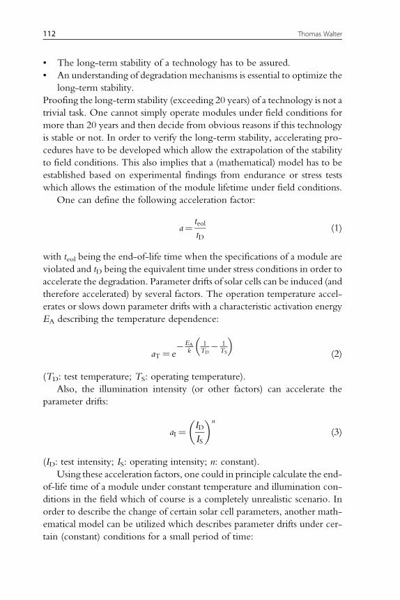
• The long-term stability of a technology has to be assured.
• An understanding of degradation mechanisms is essential to optimize the
long-term stability.
Proofing the long-term stability (exceeding 20 years) of a technology is not a
trivial task. One cannot simply operate modules under field conditions for
more than 20 years and then decide from obvious reasons if this technology
is stable or not. In order to verify the long-term stability, accelerating pro-
cedures have to be developed which allow the extrapolation of the stability
to field conditions. This also implies that a (mathematical) model has to be
established based on experimental findings from endurance or stress tests
which allows the estimation of the module lifetime under field conditions.
One can define the following acceleration factor:
a¼ teol
tD(1)
with teol being the end-of-life time when the specifications of a module are
violated and tD being the equivalent time under stress conditions in order to
accelerate the degradation. Parameter drifts of solar cells can be induced (and
therefore accelerated) by several factors. The operation temperature accel-
erates or slows down parameter drifts with a characteristic activation energy
EA describing the temperature dependence:
aT ¼ e�EA
k1TD
� 1TS
� �(2)
(TD: test temperature; TS: operating temperature).
Also, the illumination intensity (or other factors) can accelerate the
parameter drifts:
aI¼ ID
IS
� �n
(3)
(ID: test intensity; IS: operating intensity; n: constant).
Using these acceleration factors, one could in principle calculate the end-
of-life time of a module under constant temperature and illumination con-
ditions in the field which of course is a completely unrealistic scenario. In
order to describe the change of certain solar cell parameters, another math-
ematical model can be utilized which describes parameter drifts under cer-
tain (constant) conditions for a small period of time:
112 Thomas Walter
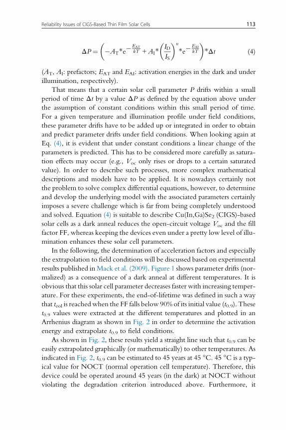
ΔP¼ �AT*e�EAT
kT +AI*ID
IS
� �n
*e�EAI
kT
� �*Δt (4)
(AT, AI: prefactors; EAT and EAI: activation energies in the dark and under
illumination, respectively).
That means that a certain solar cell parameter P drifts within a small
period of time Δt by a value ΔP as defined by the equation above under
the assumption of constant conditions within this small period of time.
For a given temperature and illumination profile under field conditions,
these parameter drifts have to be added up or integrated in order to obtain
and predict parameter drifts under field conditions. When looking again at
Eq. (4), it is evident that under constant conditions a linear change of the
parameters is predicted. This has to be considered more carefully as satura-
tion effects may occur (e.g., Voc only rises or drops to a certain saturated
value). In order to describe such processes, more complex mathematical
descriptions and models have to be applied. It is nowadays certainly not
the problem to solve complex differential equations, however, to determine
and develop the underlying model with the associated parameters certainly
imposes a severe challenge which is far from being completely understood
and solved. Equation (4) is suitable to describe Cu(In,Ga)Se2 (CIGS)-based
solar cells as a dark anneal reduces the open-circuit voltage Voc and the fill
factor FF, whereas keeping the devices even under a pretty low level of illu-
mination enhances these solar cell parameters.
In the following, the determination of acceleration factors and especially
the extrapolation to field conditions will be discussed based on experimental
results published inMack et al. (2009). Figure 1 shows parameter drifts (nor-
malized) as a consequence of a dark anneal at different temperatures. It is
obvious that this solar cell parameter decreases faster with increasing temper-
ature. For these experiments, the end-of-lifetime was defined in such a way
that teol is reached when the FF falls below 90% of its initial value (t0.9). These
t0.9 values were extracted at the different temperatures and plotted in an
Arrhenius diagram as shown in Fig. 2 in order to determine the activation
energy and extrapolate t0.9 to field conditions.
As shown in Fig. 2, these results yield a straight line such that t0.9 can be
easily extrapolated graphically (or mathematically) to other temperatures. As
indicated in Fig. 2, t0.9 can be estimated to 45 years at 45 °C. 45 °C is a typ-
ical value for NOCT (normal operation cell temperature). Therefore, this
device could be operated around 45 years (in the dark) at NOCT without
violating the degradation criterion introduced above. Furthermore, it
113Reliability Issues of CIGS-Based Thin Film Solar Cells
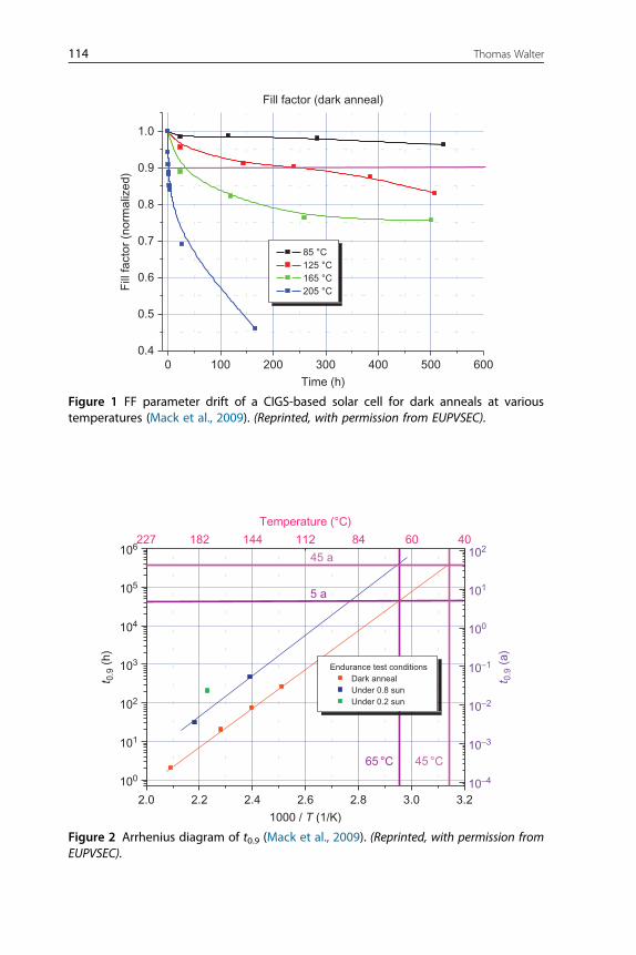
0 100 200 300 400 500 6000.4
0.5
0.6
0.7
0.8
0.9
1.0
Fill factor (dark anneal)
85 °C 125 °C 165 °C 205 °C
Time (h)
Fill
fact
or (
norm
aliz
ed)
Figure 1 FF parameter drift of a CIGS-based solar cell for dark anneals at varioustemperatures (Mack et al., 2009). (Reprinted, with permission from EUPVSEC).
2.0 2.2 2.4 2.6 2.8 3.0 3.2
100
101
102
103
104
105
106
t 0.9
(a)
65 °C
5 a
45 a
45 °C
Endurance test conditionsDark annealUnder 0.8 sunUnder 0.2 sun
1000 / T (1/K)
t 0.9
(h)
227 406084112144182
Temperature (°C)
10−4
10−3
10−2
10−1
100
101
102
Figure 2 Arrhenius diagram of t0.9 (Mack et al., 2009). (Reprinted, with permission fromEUPVSEC).
114 Thomas Walter
should be noted that t0.9 increases with illumination. Under an illumination
of 0.8 sun, an increase of t0.9 by a factor between 5 and 10 could be estimated
from Fig. 2. This enhancement of CIGS-based solar cells under illumination
is commonly observed and well known as “light soak.” Thus, this parameter
drift is not crucial for the specified lifetime of such modules. Obviously, the
number of data points in Fig. 2 is by far not sufficient to verify the stability of
this technology with statistical methods. However, it demonstrates the typ-
ical behavior of these devices with a pronounced positive impact of illumi-
nation on the long-term stability.
One important questionwhich has to be addressed concerns the possibility
to perform such acceleration experiments on a laminated module level. How-
ever, this appears to be a significant challenge as such high temperatures
(�100 °C)cannot be applied to laminatedmodules as the transformation tem-
peratures of the applied lamination foils should not be reached. Thus, it might
be possible that sufficiently high acceleration factors cannot be reached on a
module level. Therefore, unlaminated devices have to be investigated in order
to get at least an indication for the dynamics of parameter drifts in the field.
In the following, four important parameters which can have a significant
impact on the device stability will be presented and discussed:
• Metastabilities
• Partial shading and hotspots
• PID (potential-induced degradation)
• Back contact issues
2. METASTABILITIES
One of the most puzzling properties also of highly efficient CIGS-
based devices is the appearance of so-called metastabilities which have
accompanied the development of CIGS-based devices since its early days.
These metastabilities are in most cases reversible parameter drifts of primarily
Voc and FF with extremely long time constants (hours and days). These
parameter drifts are mainly initiated by a high-temperature dark storage
of the devices (dark anneal) leading to a decrease of the output power or
by keeping the modules under illumination (light soak) which improves
the performance. Regarding the reliability and also certification of a
CIGS-based technology, these parameter drifts impose a severe problem
for measurements of modules and devices. In order to verify that modules
withstand a certain stress test, the measurements prior and after the stress
have to be undertaken with the module being in the same metastable state.
115Reliability Issues of CIGS-Based Thin Film Solar Cells
Therefore, usually the modules are light-soaked for a certain time prior to
the measurements as this appears to be the “natural state” of a solar cell.
However, the duration and the conditions of such treatments are the content
of an ongoing discussion.
What is now the physics behind these metastable parameter drifts? It is
widely accepted that a change of the charge distribution in the device is
responsible for the observed parameter drifts. One model postulates ampho-
teric defect complexes which can change their charge state depending on the
position of the quasi-Fermi levels and/or optical transitions (Lany and
Zunger, 2006, 2008). The extremely long time constants associated with
thesemetastabilities are explained in terms of a configuration change as a con-
sequence of the modification of interatomic spacings. Taking the associated
capture cross sections for electrons and holes into account, a significant por-
tion of the observed metastabilities can be explained. A second model
resulting also in a change of the charge distribution is based on the existence
of mobile ions in these chalcopyrite semiconductors. Not only Cu ions but
also the extremely mobile Na are candidates for this model. It should be
noted that the existence of Na in these materials is not an unwanted and det-
rimental impurity but is one of the most important prerequisites for the suc-
cess of CIGS (Bl€osch et al., 2013; Salome et al., 2014). Recently, it was
demonstrated that a postdeposition treatment involving KF might even lead
to devices with higher efficiencies (Chirila and Reinhard, 2013).
From a first glance, these twomodels—i.e., electronic defects andmobile
ions—should be easily distinguishable. However, this discussion is still
ongoing with a lot of arguments from both sides. For a discussion on these
metastabilities, the reader should refer to the numerous literature including
some excellent review articles (Igalson et al., 2011, 2013; Kempa et al., 2013;
K€otschau et al., 2001; Moore et al., 2014).
In order to explain a certain impact of partial shading on Voc parameter
drifts, the influence of a bias across the heterojunction will be considered
in the following (Mack et al., 2009). Figure 3 shows Voc parameter drifts
of a CIGS-based solar cell under different conditions (5 h, 165 °C), from left
to right:
• In the dark unbiased
• Open-circuit conditions: 0.01 sun
• Open-circuit conditions: 0.31 sun
• Open-circuit conditions: 1 sun
• Short-circuit conditions (KS): 1 sun
• In the dark: Applied bias of +400 mV (roughly corresponding to MPP)
116 Thomas Walter
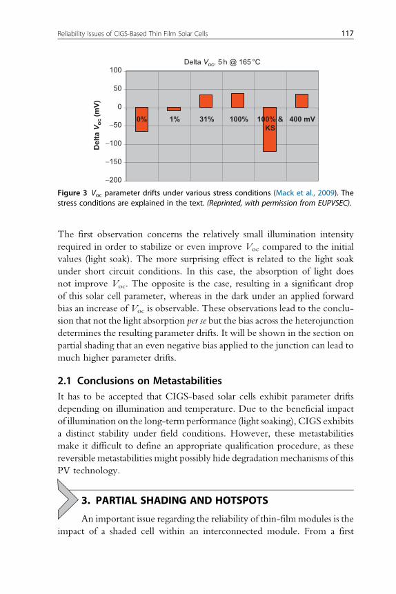
The first observation concerns the relatively small illumination intensity
required in order to stabilize or even improve Voc compared to the initial
values (light soak). The more surprising effect is related to the light soak
under short circuit conditions. In this case, the absorption of light does
not improve Voc. The opposite is the case, resulting in a significant drop
of this solar cell parameter, whereas in the dark under an applied forward
bias an increase of Voc is observable. These observations lead to the conclu-
sion that not the light absorption per se but the bias across the heterojunction
determines the resulting parameter drifts. It will be shown in the section on
partial shading that an even negative bias applied to the junction can lead to
much higher parameter drifts.
2.1 Conclusions on MetastabilitiesIt has to be accepted that CIGS-based solar cells exhibit parameter drifts
depending on illumination and temperature. Due to the beneficial impact
of illumination on the long-term performance (light soaking), CIGS exhibits
a distinct stability under field conditions. However, these metastabilities
make it difficult to define an appropriate qualification procedure, as these
reversible metastabilities might possibly hide degradation mechanisms of this
PV technology.
3. PARTIAL SHADING AND HOTSPOTS
An important issue regarding the reliability of thin-film modules is the
impact of a shaded cell within an interconnected module. From a first
Delta Voc, 5 h @ 165 °C
−200
−150
−100
−50
0
50
100
0% 1% 31% 100% 100% &
KS
400 mV
Delt
a V
oc (
mV
)
Figure 3 Voc parameter drifts under various stress conditions (Mack et al., 2009). Thestress conditions are explained in the text. (Reprinted, with permission from EUPVSEC).
117Reliability Issues of CIGS-Based Thin Film Solar Cells
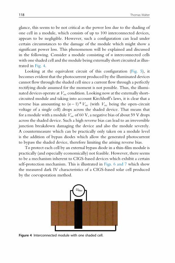
glance, this seems to be not critical as the power loss due to the shading of
one cell in a module, which consists of up to 100 interconnected devices,
appears to be negligible. However, such a configuration can lead under
certain circumstances to the damage of the module which might show a
significant power loss. This phenomenon will be explained and discussed
in the following. Consider a module consisting of n interconnected cells
with one shaded cell and the module being externally short circuited as illus-
trated in Fig. 4.
Looking at the equivalent circuit of this configuration (Fig. 5), it
becomes evident that the photocurrent produced by the illuminated devices
cannot flow through the shaded cell since a current flow through a perfectly
rectifying diode assumed for the moment is not possible. Thus, the illumi-
nated devices operate atVoc condition. Looking now at the externally short-
circuited module and taking into account Kirchhoff’s laws, it is clear that a
reverse bias amounting to (n�1)*Voc (with Voc being the open-circuit
voltage of a single cell) drops across the shaded device. That means that
for a module with a module Voc of 60 V, a negative bias of about 59 V drops
across the shaded device. Such a high reverse bias can lead to an irreversible
junction breakdown damaging the device and also the module severely.
A countermeasure which can be practically only taken on a module level
is the addition of bypass diodes which allow the generated photocurrent
to bypass the shaded device, therefore limiting the arising reverse bias.
To protect each cell by an external bypass diode in a thin-film module is
practically (and especially economically) not feasible. However, there seems
to be a mechanism inherent to CIGS-based devices which exhibit a certain
self-protection mechanism. This is illustrated in Figs. 6 and 7 which show
the measured dark IV characteristics of a CIGS-based solar cell produced
by the coevaporation method.
URev
Figure 4 Interconnected module with one shaded cell.
118 Thomas Walter
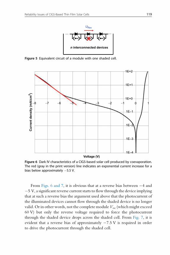
From Figs. 6 and 7, it is obvious that at a reverse bias between �4 and
�5 V, a significant reverse current starts to flow through the device implying
that at such a reverse bias the argument used above that the photocurrent of
the illuminated devices cannot flow through the shaded device is no longer
valid. Or in other words, not the complete moduleVoc (whichmight exceed
60 V) but only the reverse voltage required to force the photocurrent
through the shaded device drops across the shaded cell. From Fig. 7, it is
evident that a reverse bias of approximately �7.5 V is required in order
to drive the photocurrent through the shaded cell.
n interconnected devices
URev
Figure 5 Equivalent circuit of a module with one shaded cell.
Voltage (V)
Cu
rren
t d
en
sit
y (
mA
/cm
2)
1E−4
1E−3
1E−2
1E−1
−1−2−3−4−5−6−7−8
1E+0
10
1E+1
1E+2
Figure 6 Dark IV characteristics of a CIGS-based solar cell produced by coevaporation.The red (gray in the print version) line indicates an exponential current increase for abias below approximately �5.5 V.
119Reliability Issues of CIGS-Based Thin Film Solar Cells

A more detailed analysis of this breakdown region clearly indicates that
these reverse characteristics exhibit an exponential increase of the current
which therefore can be modeled by a reverse diode (Fig. 8) in parallel to
the principal diode (see Figs. 6 and 7). Such breakthrough characteristics
can be interpreted in terms of tunneling or avalanche currents as a result
of a high electric field in the junction region. An important aspect of those
breakthrough mechanisms is reversibility, meaning that the devices can be
operated in this current regime without permanent and irreversible damage
at least for the time of shadowing. Considering again the equivalent circuit in
Fig. 8, it can be concluded that CIGS-based devices exhibit a kind of an
inherent bypass diode limiting the possibly arising reverse bias across a
shaded cell to about�7.5 V. A question which will be discussed below con-
cerns measures to optimize this built-in bypass diode with respect to low-
ering the breakthrough voltage.
It should be noticed that not only the shading of one cell can lead to such
a reverse bias but also the inhomogeneity of the photocurrent with respect to
single cells in a thin-film module with a multitude of interconnected cells.
Voltage (V)
Cu
rren
t d
en
sit
y (
mA
/cm
2)
0 1 2
−50
−30
−10−1−2−3−4−5−6−7−8
10
30
50
70
90
110
Figure 7 Reverse IV characteristics of a CIGS-based solar cell in the dark. The horizontalred (gray in the print version) line indicates the value of the photocurrent densityresulting in a reverse bias of approximately �7.5 V across the shaded cell.
120 Thomas Walter
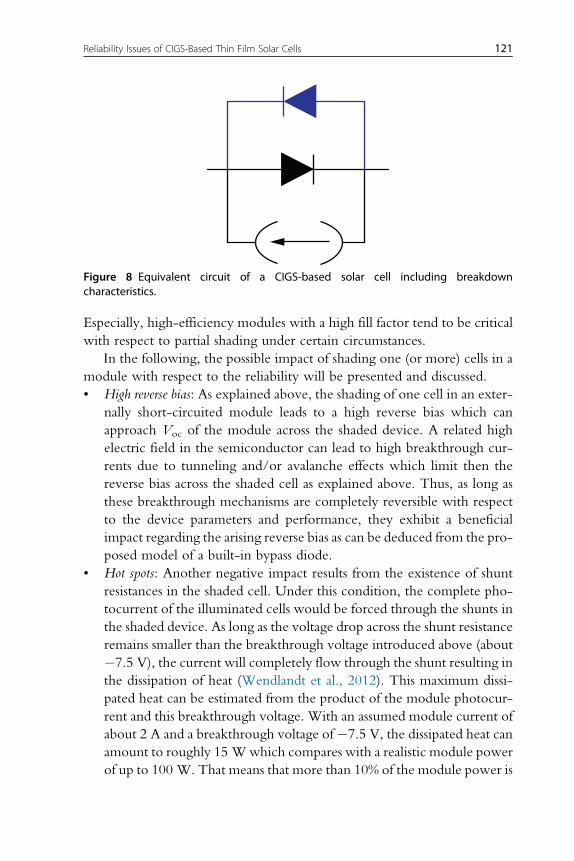
Especially, high-efficiency modules with a high fill factor tend to be critical
with respect to partial shading under certain circumstances.
In the following, the possible impact of shading one (or more) cells in a
module with respect to the reliability will be presented and discussed.
• High reverse bias: As explained above, the shading of one cell in an exter-
nally short-circuited module leads to a high reverse bias which can
approach Voc of the module across the shaded device. A related high
electric field in the semiconductor can lead to high breakthrough cur-
rents due to tunneling and/or avalanche effects which limit then the
reverse bias across the shaded cell as explained above. Thus, as long as
these breakthrough mechanisms are completely reversible with respect
to the device parameters and performance, they exhibit a beneficial
impact regarding the arising reverse bias as can be deduced from the pro-
posed model of a built-in bypass diode.
• Hot spots: Another negative impact results from the existence of shunt
resistances in the shaded cell. Under this condition, the complete pho-
tocurrent of the illuminated cells would be forced through the shunts in
the shaded device. As long as the voltage drop across the shunt resistance
remains smaller than the breakthrough voltage introduced above (about
�7.5 V), the current will completely flow through the shunt resulting in
the dissipation of heat (Wendlandt et al., 2012). This maximum dissi-
pated heat can be estimated from the product of the module photocur-
rent and this breakthrough voltage. With an assumed module current of
about 2 A and a breakthrough voltage of�7.5 V, the dissipated heat can
amount to roughly 15 Wwhich compares with a realistic module power
of up to 100 W. That means that more than 10% of the module power is
Figure 8 Equivalent circuit of a CIGS-based solar cell including breakdowncharacteristics.
121Reliability Issues of CIGS-Based Thin Film Solar Cells
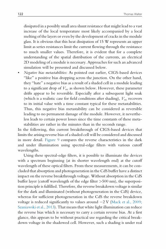
dissipated in a possibly small area shunt resistance that might lead to a vast
increase of the local temperature most likely accompanied by a local
melting of the layers or even by the development of cracks in the module
glass. It is obvious that this heat dissipation of 15 W represents an upper
limit as series resistances limit the current flowing through the resistance
to much smaller values. Therefore, it is evident that for a complete
understanding of the spatial distribution of the currents, an electrical
2D modeling of a module is necessary. Approaches for such an advanced
simulation will be presented and discussed below.
• Negative bias metastabilities: As pointed out earlier, CIGS-based devices
“like” a positive bias dropping across the junction. On the other hand,
they “hate” a negative bias as a result of a shaded cell in a module leading
to a significant drop of Voc as shown below. However, these parameter
drifts appear to be reversible. Especially after a subsequent light soak
(which is a realistic case for field conditions after shading), Voc recovers
to its initial value with a time constant typical for these metastabilities.
Thus, this negative bias metastability can be considered as reversible
leading to no permanent damage of the module. However, it neverthe-
less leads to certain power losses since the time constants of these meta-
stabilities are rather in the minutes than in the seconds range.
In the following, this current breakthrough of CIGS-based devices that
limits the arising reverse bias of a shaded cell will be considered and discussed
in more detail. Figure 9 compares the reverse characteristics in the dark
and under illumination using spectral-edge filters with various cutoff
wavelengths.
Using these spectral-edge filters, it is possible to illuminate the devices
with a spectrum beginning (at its shorter wavelength end) at the cutoff
wavelength of these optical filters. From these measurements, it can be con-
cluded that absorption and photogeneration in the CdS buffer have a distinct
impact on the reverse breakthrough voltage. Without absorption in the CdS
buffer layer (cutoff wavelength of the edge filter >500 nm), the superposi-
tion principle is fulfilled. Therefore, the reverse breakdown voltage is similar
for the dark and illuminated (without photogeneration in the CdS) device,
whereas for sufficient photogeneration in the CdS the reverse breakdown
voltage is reduced significantly to values around �2 V (Mack et al., 2009;
Szaniawski et al., 2013). That means that white light illumination can reduce
the reverse bias which is necessary to carry a certain reverse bias. At a first
glance, this appears to be without practical use regarding the critical break-
down voltage in the shadowed cell. However, such a shading is under real
122 Thomas Walter
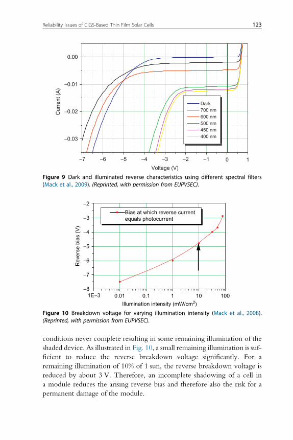
conditions never complete resulting in some remaining illumination of the
shaded device. As illustrated in Fig. 10, a small remaining illumination is suf-
ficient to reduce the reverse breakdown voltage significantly. For a
remaining illumination of 10% of 1 sun, the reverse breakdown voltage is
reduced by about 3 V. Therefore, an incomplete shadowing of a cell in
a module reduces the arising reverse bias and therefore also the risk for a
permanent damage of the module.
−7 −6 −5 −4 −3 −2 −1 0 1
−0.03
−0.02
−0.01
0.00
Dark700 nm600 nm500 nm450 nm400 nm
Cur
rent
(A
)
Voltage (V)
Figure 9 Dark and illuminated reverse characteristics using different spectral filters(Mack et al., 2009). (Reprinted, with permission from EUPVSEC).
1E−3−8
−7
−6
−5
−4
−3
−2
0.01 0.1
Bias at which reverse currentequals photocurrent
Illumination intensity (mW/cm2)
Rev
erse
bia
s (V
)
1 10 100
Figure 10 Breakdown voltage for varying illumination intensity (Mack et al., 2008).(Reprinted, with permission from EUPVSEC).
123Reliability Issues of CIGS-Based Thin Film Solar Cells
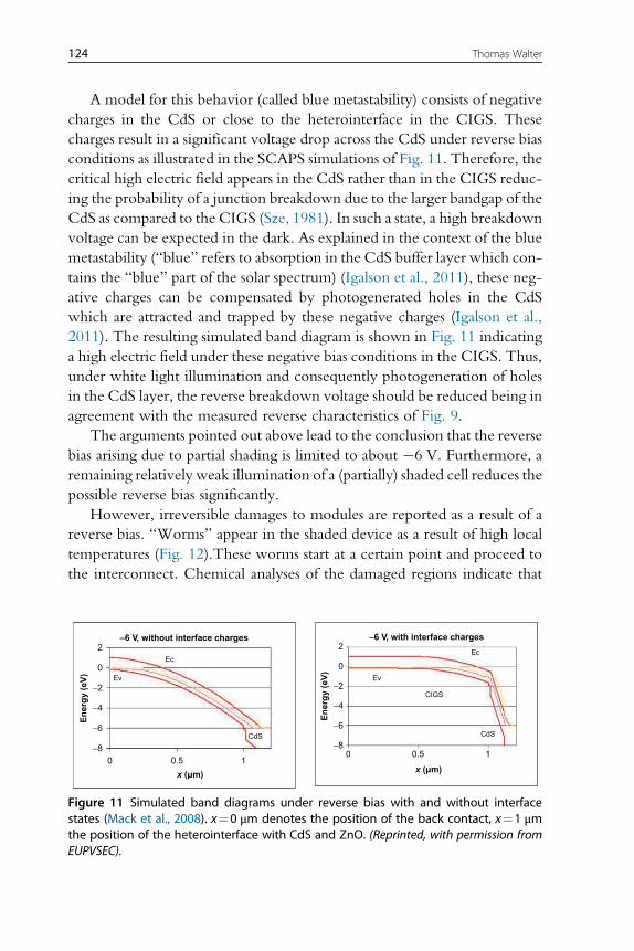
A model for this behavior (called blue metastability) consists of negative
charges in the CdS or close to the heterointerface in the CIGS. These
charges result in a significant voltage drop across the CdS under reverse bias
conditions as illustrated in the SCAPS simulations of Fig. 11. Therefore, the
critical high electric field appears in the CdS rather than in the CIGS reduc-
ing the probability of a junction breakdown due to the larger bandgap of the
CdS as compared to the CIGS (Sze, 1981). In such a state, a high breakdown
voltage can be expected in the dark. As explained in the context of the blue
metastability (“blue” refers to absorption in the CdS buffer layer which con-
tains the “blue” part of the solar spectrum) (Igalson et al., 2011), these neg-
ative charges can be compensated by photogenerated holes in the CdS
which are attracted and trapped by these negative charges (Igalson et al.,
2011). The resulting simulated band diagram is shown in Fig. 11 indicating
a high electric field under these negative bias conditions in the CIGS. Thus,
under white light illumination and consequently photogeneration of holes
in the CdS layer, the reverse breakdown voltage should be reduced being in
agreement with the measured reverse characteristics of Fig. 9.
The arguments pointed out above lead to the conclusion that the reverse
bias arising due to partial shading is limited to about �6 V. Furthermore, a
remaining relatively weak illumination of a (partially) shaded cell reduces the
possible reverse bias significantly.
However, irreversible damages to modules are reported as a result of a
reverse bias. “Worms” appear in the shaded device as a result of high local
temperatures (Fig. 12).These worms start at a certain point and proceed to
the interconnect. Chemical analyses of the damaged regions indicate that
0−8
−6
−4
−2
0
2
0.5
x (µm)
-6 V, without interface charges
En
erg
y (
eV
)
1
CdS
CIGS
Ev
Ec
0−8
−6
−4
−2
0
2
0.5
x (µm)
-6 V, with interface charges
En
erg
y (
eV
)
1
CdS
Ev
Ec
Figure 11 Simulated band diagrams under reverse bias with and without interfacestates (Mack et al., 2008). x¼0 μm denotes the position of the back contact, x¼1 μmthe position of the heterointerface with CdS and ZnO. (Reprinted, with permission fromEUPVSEC).
124 Thomas Walter
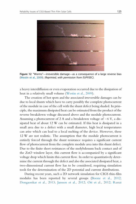
a heavy interdiffusion or even evaporation occurred due to the dissipation of
heat in a relatively small volume (Westin et al., 2009).
The creation of hot spots and the associated irreversible damages can be
due to local shunts which have to carry possibly the complete photocurrent
of the module in case of the cell with the shunt defect being shaded. In prin-
ciple, the maximum dissipated heat can be estimated from the product of the
reverse breakdown voltage discussed above and the module photocurrent.
Assuming a photocurrent of 2 A and a breakdown voltage of �6 V, a dis-
sipated heat of about 12 W can be estimated. If this heat is dissipated in a
small area due to a defect with a small diameter, high local temperatures
can arise which can lead to a local melting of the device. However, these
12 W are not realistic. The assumption that the module photocurrent is
entirely forced through the shunt resistance requires a significant current
flow of photocurrent from the complete module area into this shunt defect.
Due to the finite sheet resistances of the molybdenum back contact and of
the ZnO window layer, this current flow is accompanied by a significant
voltage drop which limits this current flow. In order to quantitatively deter-
mine the current through the defect and also the associated dissipated heat, a
two-dimensional current flow has to be considered, requiring simulation
tools for the determination of the 2D potential and current distributions.
During recent years, such a 2D network simulation for CIGS thin-film
modules has been reported by several groups (Boone et al., 2012;
Dongaonkar et al., 2013; Janssen et al., 2012; Ott et al., 2012; Runai
Figure 12 “Worms”—irreversible damage—as a consequence of a large reverse bias(Westin et al., 2009). (Reprinted, with permission from EUPVSEC).
125Reliability Issues of CIGS-Based Thin Film Solar Cells
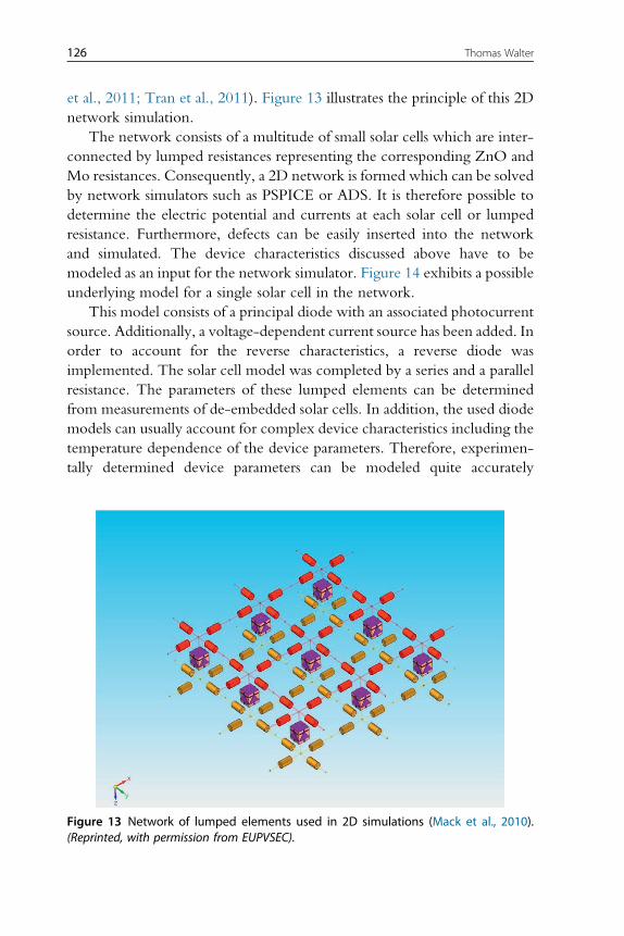
et al., 2011; Tran et al., 2011). Figure 13 illustrates the principle of this 2D
network simulation.
The network consists of a multitude of small solar cells which are inter-
connected by lumped resistances representing the corresponding ZnO and
Mo resistances. Consequently, a 2D network is formed which can be solved
by network simulators such as PSPICE or ADS. It is therefore possible to
determine the electric potential and currents at each solar cell or lumped
resistance. Furthermore, defects can be easily inserted into the network
and simulated. The device characteristics discussed above have to be
modeled as an input for the network simulator. Figure 14 exhibits a possible
underlying model for a single solar cell in the network.
This model consists of a principal diode with an associated photocurrent
source. Additionally, a voltage-dependent current source has been added. In
order to account for the reverse characteristics, a reverse diode was
implemented. The solar cell model was completed by a series and a parallel
resistance. The parameters of these lumped elements can be determined
from measurements of de-embedded solar cells. In addition, the used diode
models can usually account for complex device characteristics including the
temperature dependence of the device parameters. Therefore, experimen-
tally determined device parameters can be modeled quite accurately
x
yz
Figure 13 Network of lumped elements used in 2D simulations (Mack et al., 2010).(Reprinted, with permission from EUPVSEC).
126 Thomas Walter
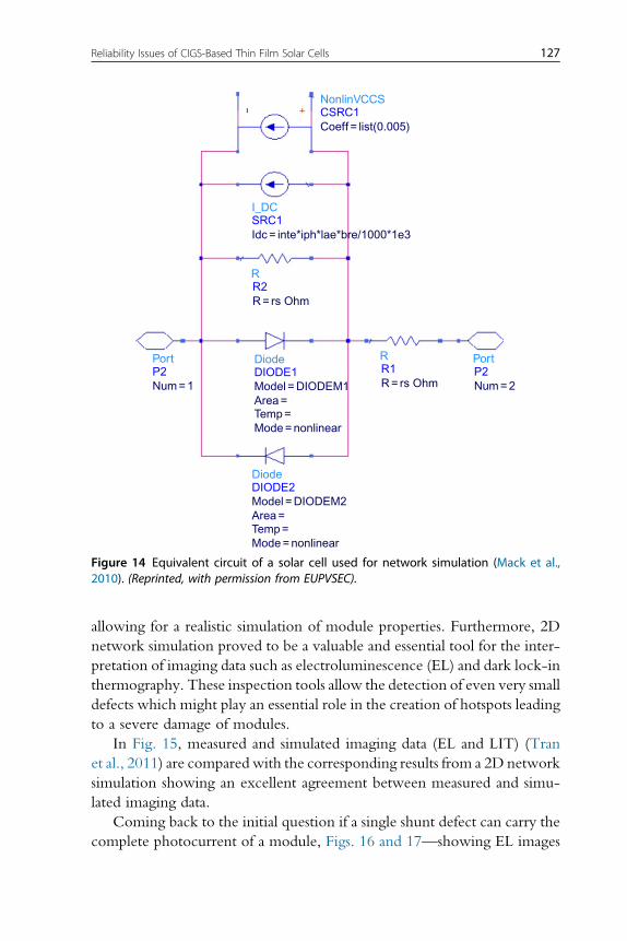
allowing for a realistic simulation of module properties. Furthermore, 2D
network simulation proved to be a valuable and essential tool for the inter-
pretation of imaging data such as electroluminescence (EL) and dark lock-in
thermography. These inspection tools allow the detection of even very small
defects which might play an essential role in the creation of hotspots leading
to a severe damage of modules.
In Fig. 15, measured and simulated imaging data (EL and LIT) (Tran
et al., 2011) are compared with the corresponding results from a 2D network
simulation showing an excellent agreement between measured and simu-
lated imaging data.
Coming back to the initial question if a single shunt defect can carry the
complete photocurrent of a module, Figs. 16 and 17—showing EL images
DiodeDIODE2Model = DIODEM2
Temp =Mode = nonlinear
Area =
Diode RDIODE1 R1
Model = DIODEM1 R = rs Ohm
RR2R = rs Ohm
I_DCSRC1Idc = inte*iph*lae*bre/1000*1e3
NonlinVCCSCSRC1Coeff = list(0.005)
PortP2Num = 2
PortP2Num = 1
Temp =Mode = nonlinear
Area =
Figure 14 Equivalent circuit of a solar cell used for network simulation (Mack et al.,2010). (Reprinted, with permission from EUPVSEC).
127Reliability Issues of CIGS-Based Thin Film Solar Cells

Figure 15 Measured and simulated EL and LIT images (Tran et al., 2011). (Reprinted, withpermission from EUPVSEC).
Figure 16 EL image for low current injection (Mack et al., 2010). (Reprinted, with permis-sion from EUPVSEC).
128 Thomas Walter
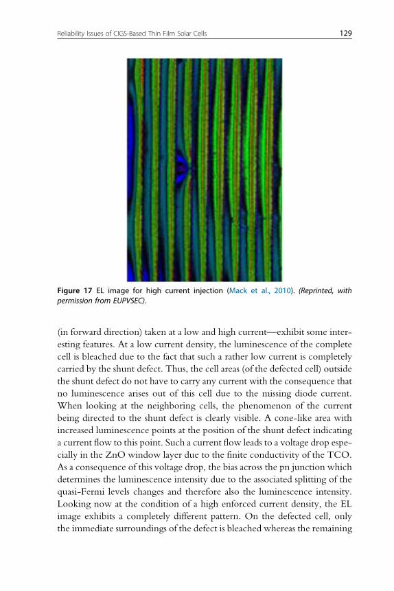
(in forward direction) taken at a low and high current—exhibit some inter-
esting features. At a low current density, the luminescence of the complete
cell is bleached due to the fact that such a rather low current is completely
carried by the shunt defect. Thus, the cell areas (of the defected cell) outside
the shunt defect do not have to carry any current with the consequence that
no luminescence arises out of this cell due to the missing diode current.
When looking at the neighboring cells, the phenomenon of the current
being directed to the shunt defect is clearly visible. A cone-like area with
increased luminescence points at the position of the shunt defect indicating
a current flow to this point. Such a current flow leads to a voltage drop espe-
cially in the ZnO window layer due to the finite conductivity of the TCO.
As a consequence of this voltage drop, the bias across the pn junction which
determines the luminescence intensity due to the associated splitting of the
quasi-Fermi levels changes and therefore also the luminescence intensity.
Looking now at the condition of a high enforced current density, the EL
image exhibits a completely different pattern. On the defected cell, only
the immediate surroundings of the defect is bleached whereas the remaining
Figure 17 EL image for high current injection (Mack et al., 2010). (Reprinted, withpermission from EUPVSEC).
129Reliability Issues of CIGS-Based Thin Film Solar Cells
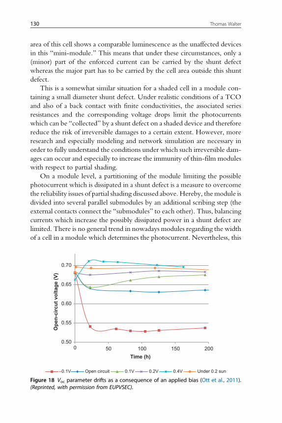
area of this cell shows a comparable luminescence as the unaffected devices
in this “mini-module.” This means that under these circumstances, only a
(minor) part of the enforced current can be carried by the shunt defect
whereas the major part has to be carried by the cell area outside this shunt
defect.
This is a somewhat similar situation for a shaded cell in a module con-
taining a small diameter shunt defect. Under realistic conditions of a TCO
and also of a back contact with finite conductivities, the associated series
resistances and the corresponding voltage drops limit the photocurrents
which can be “collected” by a shunt defect on a shaded device and therefore
reduce the risk of irreversible damages to a certain extent. However, more
research and especially modeling and network simulation are necessary in
order to fully understand the conditions under which such irreversible dam-
ages can occur and especially to increase the immunity of thin-film modules
with respect to partial shading.
On a module level, a partitioning of the module limiting the possible
photocurrent which is dissipated in a shunt defect is a measure to overcome
the reliability issues of partial shading discussed above. Hereby, the module is
divided into several parallel submodules by an additional scribing step (the
external contacts connect the “submodules” to each other). Thus, balancing
currents which increase the possibly dissipated power in a shunt defect are
limited. There is no general trend in nowadays modules regarding the width
of a cell in a module which determines the photocurrent. Nevertheless, this
0.50
0.55
0.60
0.65
0.70
0 50 100 150 200
Op
en
-cir
cu
t vo
ltag
e (
V)
Time (h)
−0.1V Open circuit 0.1V 0.2V 0.4V Under 0.2 sun
Figure 18 Voc parameter drifts as a consequence of an applied bias (Ott et al., 2011).(Reprinted, with permission from EUPVSEC).
130 Thomas Walter
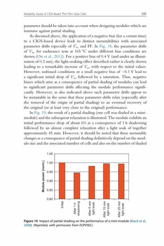
parameter should be taken into account when designing modules which are
immune against partial shading.
As discussed above, the application of a negative bias (for a certain time)
to a CIGS-based device leads to distinct metastabilities with associated
parameter drifts especially of Voc and FF. In Fig. 18, the parameter drifts
of Voc for endurance tests at 165 °C under different bias conditions are
shown (Ott et al., 2011). For a positive bias of 0.4 V (and under an illumi-
nation of 0.2 sun), the light-soaking effect described earlier is clearly shown
leading to a remarkable increase of Voc with respect to the initial values.
However, unbiased conditions or a small negative bias of �0.1 V lead to
a significant initial drop of Voc followed by a saturation. Thus, negative
biases which arise as a consequence of partial shading of modules can lead
to significant parameter drifts affecting the module performance signifi-
cantly. However, as also indicated above such parameter drifts appear to
be metastable in the sense that these parameter drifts relax (especially after
the removal of the origin of partial shading) to an eventual recovery of
the original (or at least very close to the original) performance.
In Fig. 19, the result of a partial shading (one cell was shaded in a mini-
module) and the subsequent relaxation is illustrated. The module exhibits an
initial performance drop of about 6% as a consequence of 1 h shadowing
followed by an almost complete relaxation after a light soak of together
approximately 45 min. However, it should be noted that these metastable
changes as a consequence of partial shading definitively depend on the mod-
ule size and the associated number of cells and also on the number of shaded
0.80
0.85
0.90
0.95
1.00
1.05
Initi
al
Afte
r 1
hsh
adow
ing
Afte
r 5
min
light
soa
k
Afte
r 15
min
light
soa
k
Afte
r 25
min
light
soa
k
Mo
du
le p
ow
er
(no
rm.)
Figure 19 Impact of partial shading on the performance of a mini-module (Mack et al.,2008). (Reprinted, with permission from EUPVSEC).
131Reliability Issues of CIGS-Based Thin Film Solar Cells
cells. Therefore, more research is needed to fully understand these metasta-
ble changes of the module performance and even more important is to eval-
uate the significance of this mechanism under real field conditions including
daily cycles of shading followed by illumination and the associated relaxa-
tion. In (Dongaonkar et al., 2012) similar metastable parameter drifts as a
result of negative bias stress were reported.
3.1 Conclusions on Partial ShadingPartial shading seems to be an inherent problem of thin-film technologies as
single cells cannot be protected individually by a bypass diode. However,
CIGS exhibits favorable reverse characteristics which limit the possible
reverse bias across one shaded cell in a module. Nevertheless, irreversible
breakthroughs have been reported which might be related to small defects.
2D network simulations seem to be a viable tool for the understanding of 2D
current flows in a module which have to be understood in order to classify
defects with respect to hotspots. Also, negative bias metastabilities might
occur as a consequence of partial shading.
4. POTENTIAL-INDUCED DEGRADATION
PID is a mechanism which can lead to a dramatic damage of affected
PVmodules. Hereby, a potential drop across the front or substrate glass leads
to a leakage current associated with mobile Na ions in the glass. PID was first
discovered in highly efficient monocrystalline Si modules (Pingel et al.,
2010). Nevertheless, it was pointed out that these parameter drifts were
reversible leading to a complete recovery of the initial module performance.
For thin-film Si modules, irreversible damage was reported as a result of
TCO corrosion associated with the out-diffusion of Na from the cover glass
into the TCO where a reaction with in-diffused water occurred. However,
PID is not only restricted to Si-based technologies but can be observed for
almost all PV technologies. For CIGS, only a few publications exist regard-
ing the impact of PID on the module performance (Fjallstrom et al., 2013;
Lechner et al., 2013). The latter publication is based on research undertaken
at the Angstrom Center in Uppsala, Sweden. It was clearly shown in this
publication (Fjallstrom et al., 2013) that the efficiency of CIGS-based
devices deposited by simultaneous evaporation could be reduced to
“zero” by applying a positive bias onto the back side of the glass substrate
with respect to the Mo back contact. Hereby, the high voltage was applied
between the Mo back contact and a metallic tape attached to the backside of
132 Thomas Walter

the substrate glass. This is shown in Fig. 20 which also clearly points out that
this degradation is related to the amount of Na in the glass substrate (as can be
deduced from the different substrate glasses). In other words, the use of
Na-free or Na-poor substrate glasses results in an immunity against PID,
whereas substrates with a higher Na content are affected by this severe deg-
radation mechanism.
A closer look at the degraded IV characteristics as illustrated in Fig. 21
reveals that PID primarily affects Voc (and FF) in the initial phase (compare,
for example, the 24-h case) followed by an additional decrease of the pho-
tocurrent in the final stadium which is characterized by an almost negligible
Voc. This decrease of Voc could be at a first sight attributed to a significantly
reduced minority carrier lifetime. However, this should also have a severe
impact on the diffusion length and therefore on the photocurrent collection
which is not really the case when looking at Fig. 21 in the initial degradation
phase. Alternatively, a significant reduction of the net acceptor density could
also explain this severe parameter drift of Voc as with a decreasing net accep-
tor density in the absorber the barrier in the junction decreases which then
reduces Voc. At least in the initial stage of the degradation, this mechanism
00.0
0.1
0.2
0.3
0.4
0.5
0.6
Nor
mal
ized
initi
al e
ffic
ienc
y
0.7
0.8
1.0
0.9
10 20
Duration of stress (h)
1—SLG
2—High Na
4—Na-free
3—Na only
5—Low Na
30 40 50
Figure 20 PID parameter drifts for various glass substrates (SLG: soda lime glass).Copyright IEEE 2013. Reprinted, with permission, from Fjallstrom et al. (2013).
133Reliability Issues of CIGS-Based Thin Film Solar Cells
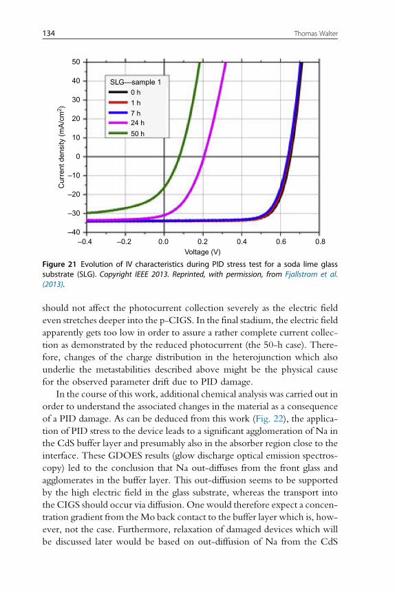
should not affect the photocurrent collection severely as the electric field
even stretches deeper into the p-CIGS. In the final stadium, the electric field
apparently gets too low in order to assure a rather complete current collec-
tion as demonstrated by the reduced photocurrent (the 50-h case). There-
fore, changes of the charge distribution in the heterojunction which also
underlie the metastabilities described above might be the physical cause
for the observed parameter drift due to PID damage.
In the course of this work, additional chemical analysis was carried out in
order to understand the associated changes in the material as a consequence
of a PID damage. As can be deduced from this work (Fig. 22), the applica-
tion of PID stress to the device leads to a significant agglomeration of Na in
the CdS buffer layer and presumably also in the absorber region close to the
interface. These GDOES results (glow discharge optical emission spectros-
copy) led to the conclusion that Na out-diffuses from the front glass and
agglomerates in the buffer layer. This out-diffusion seems to be supported
by the high electric field in the glass substrate, whereas the transport into
the CIGS should occur via diffusion. One would therefore expect a concen-
tration gradient from theMo back contact to the buffer layer which is, how-
ever, not the case. Furthermore, relaxation of damaged devices which will
be discussed later would be based on out-diffusion of Na from the CdS
–0.4–40
–30
–20
–10
0
10
20
50 h
24 h7 h
1 h
0 h
SLG—sample 1
30
40
50
–0.2 0.0 0.2Voltage (V)
Cur
rent
den
sity
(m
A/c
m2 )
0.4 0.6 0.8
Figure 21 Evolution of IV characteristics during PID stress test for a soda lime glasssubstrate (SLG). Copyright IEEE 2013. Reprinted, with permission, from Fjallstrom et al.(2013).
134 Thomas Walter

buffer layer. However, what should be the driving force for such a process?
In principle, diffusion is from a thermodynamic point of view irreversible. It
is therefore hard to explain that PID-damaged CIGS can relax. In an addi-
tional work of the group in Uppsala, GDOES studies were performed after
an almost complete relaxation of a severely damaged device showing a very
similar Na distribution as measured in the damaged state. These consider-
ations make clear that the microscopic origin of the PID damage is not
yet understood. Similar to existing models for PID damage of crystalline
Si solar cells, models involving the out-diffusion of Na or models based
on pure charging mechanisms are discussed. However, so far the published
results cannot exclude or verify either of these models.
Table 1 clearly shows that the overwhelming part of the damage could be
restored after 6 months under lab conditions without additional measures
Table 1 PID Parameter DriftsVoc (mV) jsc (mA/cm2) FF (%) Efficiency (%)
As grown 628 32.87 75.2 15.5
After PID 22 4.43 28.4 0.0
6 months after PID 581 33.14 73.6 14.2
Copyright IEEE 2013. Reprinted, with permission, from Fjallstrom et al. (2013).
Sputtering time (a.u.)
Cou
nts
(a.u
.)
Na PIDNa controlCdMoSe
CdS CIGS Mo
Figure 22 GDOES depth profile prior and after PID stress test. Copyright IEEE 2013.Reprinted, with permission, from Fjallstrom et al. (2013).
135Reliability Issues of CIGS-Based Thin Film Solar Cells
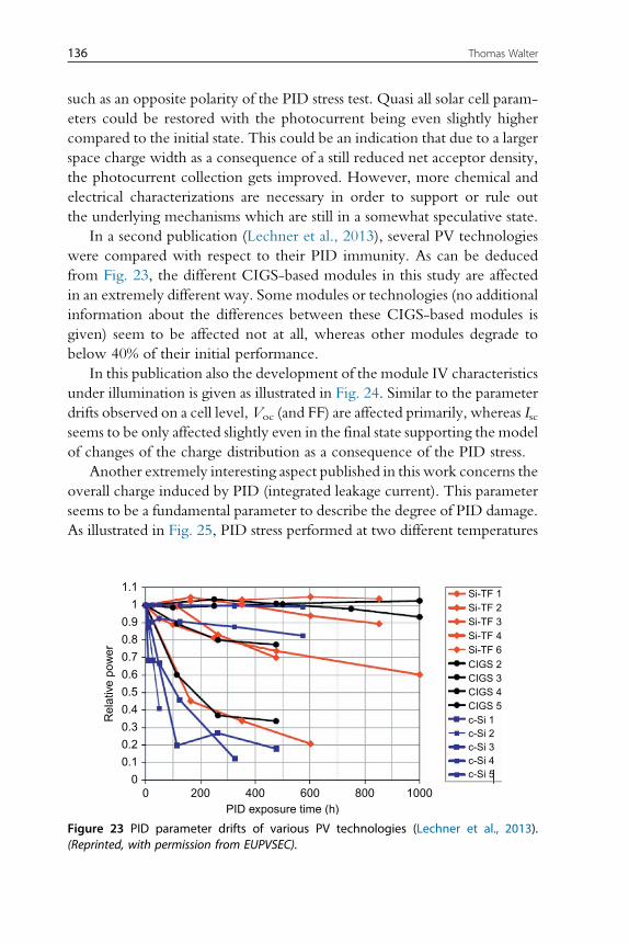
such as an opposite polarity of the PID stress test. Quasi all solar cell param-
eters could be restored with the photocurrent being even slightly higher
compared to the initial state. This could be an indication that due to a larger
space charge width as a consequence of a still reduced net acceptor density,
the photocurrent collection gets improved. However, more chemical and
electrical characterizations are necessary in order to support or rule out
the underlying mechanisms which are still in a somewhat speculative state.
In a second publication (Lechner et al., 2013), several PV technologies
were compared with respect to their PID immunity. As can be deduced
from Fig. 23, the different CIGS-based modules in this study are affected
in an extremely different way. Some modules or technologies (no additional
information about the differences between these CIGS-based modules is
given) seem to be affected not at all, whereas other modules degrade to
below 40% of their initial performance.
In this publication also the development of the module IV characteristics
under illumination is given as illustrated in Fig. 24. Similar to the parameter
drifts observed on a cell level,Voc (and FF) are affected primarily, whereas Iscseems to be only affected slightly even in the final state supporting the model
of changes of the charge distribution as a consequence of the PID stress.
Another extremely interesting aspect published in this work concerns the
overall charge induced by PID (integrated leakage current). This parameter
seems to be a fundamental parameter to describe the degree of PID damage.
As illustrated in Fig. 25, PID stress performed at two different temperatures
00
0.1
0.2
0.3
0.4
0.5
0.6
0.7
0.8
0.9
1
1.1
200 400PID exposure time (h)
Rel
ativ
e po
wer
600 800 1000
Si-TF 1Si-TF 2Si-TF 3Si-TF 4Si-TF 6
CIGS 2CIGS 3CIGS 4CIGS 5c-Si 1c-Si 2c-Si 3c-Si 4c-Si 5
Figure 23 PID parameter drifts of various PV technologies (Lechner et al., 2013).(Reprinted, with permission from EUPVSEC).
136 Thomas Walter
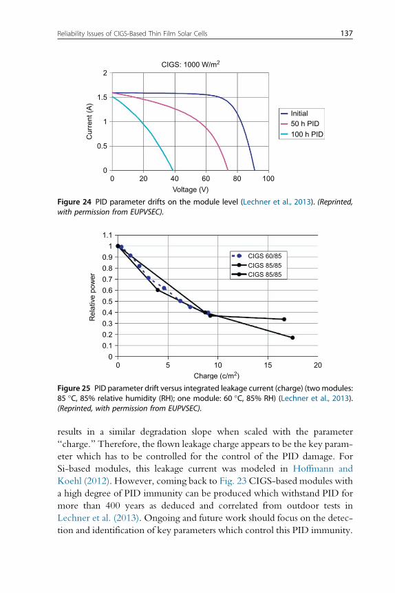
results in a similar degradation slope when scaled with the parameter
“charge.” Therefore, the flown leakage charge appears to be the key param-
eter which has to be controlled for the control of the PID damage. For
Si-based modules, this leakage current was modeled in Hoffmann and
Koehl (2012). However, coming back to Fig. 23 CIGS-based modules with
a high degree of PID immunity can be produced which withstand PID for
more than 400 years as deduced and correlated from outdoor tests in
Lechner et al. (2013). Ongoing and future work should focus on the detec-
tion and identification of key parameters which control this PID immunity.
00
0.1
0.2
0.3
0.4
0.5
0.6
0.7
0.8
0.9
1
1.1
5 10
Charge (c/m2)
Rel
ativ
e po
wer
15
CIGS 60/85
CIGS 85/85CIGS 85/85
20
Figure 25 PID parameter drift versus integrated leakage current (charge) (twomodules:85 °C, 85% relative humidity (RH); one module: 60 °C, 85% RH) (Lechner et al., 2013).(Reprinted, with permission from EUPVSEC).
00
0.5
1
1.5
2
20 40
Voltage (V)
CIGS: 1000 W/m2
Cur
rent
(A
)
60 80 100
Initial50 h PID
100 h PID
Figure 24 PID parameter drifts on the module level (Lechner et al., 2013). (Reprinted,with permission from EUPVSEC).
137Reliability Issues of CIGS-Based Thin Film Solar Cells
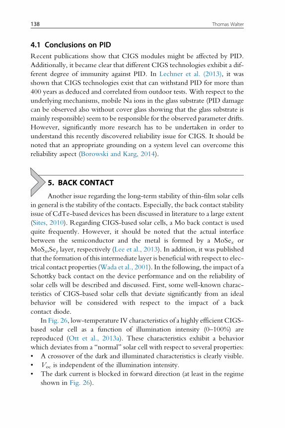
4.1 Conclusions on PIDRecent publications show that CIGS modules might be affected by PID.
Additionally, it became clear that different CIGS technologies exhibit a dif-
ferent degree of immunity against PID. In Lechner et al. (2013), it was
shown that CIGS technologies exist that can withstand PID for more than
400 years as deduced and correlated from outdoor tests. With respect to the
underlying mechanisms, mobile Na ions in the glass substrate (PID damage
can be observed also without cover glass showing that the glass substrate is
mainly responsible) seem to be responsible for the observed parameter drifts.
However, significantly more research has to be undertaken in order to
understand this recently discovered reliability issue for CIGS. It should be
noted that an appropriate grounding on a system level can overcome this
reliability aspect (Borowski and Karg, 2014).
5. BACK CONTACT
Another issue regarding the long-term stability of thin-film solar cells
in general is the stability of the contacts. Especially, the back contact stability
issue of CdTe-based devices has been discussed in literature to a large extent
(Sites, 2010). Regarding CIGS-based solar cells, a Mo back contact is used
quite frequently. However, it should be noted that the actual interface
between the semiconductor and the metal is formed by a MoSex or
MoSx,Sey layer, respectively (Lee et al., 2013). In addition, it was published
that the formation of this intermediate layer is beneficial with respect to elec-
trical contact properties (Wada et al., 2001). In the following, the impact of a
Schottky back contact on the device performance and on the reliability of
solar cells will be described and discussed. First, some well-known charac-
teristics of CIGS-based solar cells that deviate significantly from an ideal
behavior will be considered with respect to the impact of a back
contact diode.
In Fig. 26, low-temperature IV characteristics of a highly efficient CIGS-
based solar cell as a function of illumination intensity (0–100%) are
reproduced (Ott et al., 2013a). These characteristics exhibit a behavior
which deviates from a “normal” solar cell with respect to several properties:
• A crossover of the dark and illuminated characteristics is clearly visible.
• Voc is independent of the illumination intensity.
• The dark current is blocked in forward direction (at least in the regime
shown in Fig. 26).
138 Thomas Walter
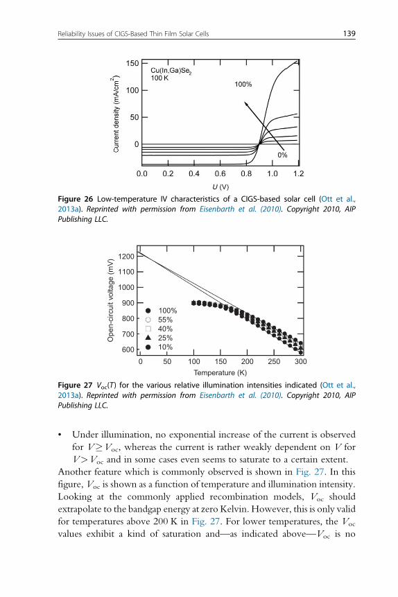
• Under illumination, no exponential increase of the current is observed
for V�Voc, whereas the current is rather weakly dependent on V for
V>Voc and in some cases even seems to saturate to a certain extent.
Another feature which is commonly observed is shown in Fig. 27. In this
figure, Voc is shown as a function of temperature and illumination intensity.
Looking at the commonly applied recombination models, Voc should
extrapolate to the bandgap energy at zero Kelvin. However, this is only valid
for temperatures above 200 K in Fig. 27. For lower temperatures, the Voc
values exhibit a kind of saturation and—as indicated above—Voc is no
0
600
Ope
n-ci
rcui
t vol
tage
(m
V)
700
800
900
1000
1100
1200
50
100%55%40%25%10%
100
Temperature (K)
150 200 250 300
Figure 27 Voc(T) for the various relative illumination intensities indicated (Ott et al.,2013a). Reprinted with permission from Eisenbarth et al. (2010). Copyright 2010, AIPPublishing LLC.
Figure 26 Low-temperature IV characteristics of a CIGS-based solar cell (Ott et al.,2013a). Reprinted with permission from Eisenbarth et al. (2010). Copyright 2010, AIPPublishing LLC.
139Reliability Issues of CIGS-Based Thin Film Solar Cells
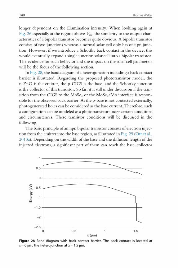
longer dependent on the illumination intensity. When looking again at
Fig. 26 especially at the regime above Voc, the similarity to the output char-
acteristics of a bipolar transistor becomes quite obvious. A bipolar transistor
consists of two junctions whereas a normal solar cell only has one pn junc-
tion. However, if we introduce a Schottky back contact in the device, this
would eventually expand a single junction solar cell into a bipolar transistor.
The evidence for such behavior and the impact on the solar cell parameters
will be the focus of the following section.
In Fig. 28, the band diagram of a heterojunction including a back contact
barrier is illustrated. Regarding the proposed phototransistor model, the
n-ZnO is the emitter, the p-CIGS is the base, and the Schottky junction
is the collector of this transistor. So far, it is still under discussion if the tran-
sition from the CIGS to the MoSex or the MoSex/Mo interface is respon-
sible for the observed back barrier. As the p-base is not contacted externally,
photogenerated holes can be considered as the base current. Therefore, such
a configuration can be modeled as a phototransistor under certain conditions
and circumstances. These transistor conditions will be discussed in the
following.
The basic principle of an npn bipolar transistor consists of electron injec-
tion from the emitter into the base region, as illustrated in Fig. 29 (Ott et al.,
2013a). Depending on the width of the base and the diffusion length of the
injected electrons, a significant part of them can reach the base–collector
0 0.5 1x (µm)
1.5-2.5
-2
-1.5
-1
-0.5
0
En
erg
y (
eV
)
0.5
1
Figure 28 Band diagram with back contact barrier. The back contact is located atx¼0 μm, the heterojunction at x¼1.5 μm.
140 Thomas Walter
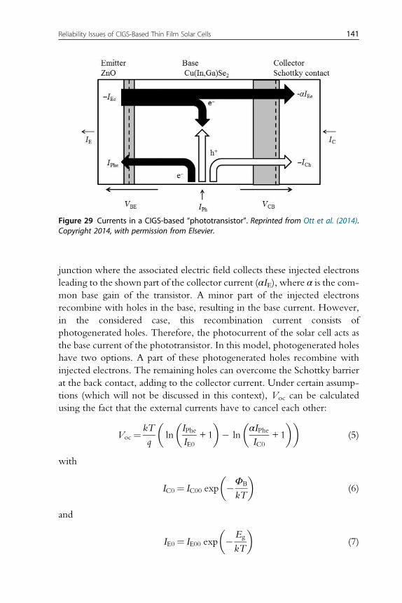
junction where the associated electric field collects these injected electrons
leading to the shown part of the collector current (αIE), where α is the com-
mon base gain of the transistor. A minor part of the injected electrons
recombine with holes in the base, resulting in the base current. However,
in the considered case, this recombination current consists of
photogenerated holes. Therefore, the photocurrent of the solar cell acts as
the base current of the phototransistor. In this model, photogenerated holes
have two options. A part of these photogenerated holes recombine with
injected electrons. The remaining holes can overcome the Schottky barrier
at the back contact, adding to the collector current. Under certain assump-
tions (which will not be discussed in this context), Voc can be calculated
using the fact that the external currents have to cancel each other:
Voc¼ kT
qln
IPhe
IE0+ 1
� �� ln
αIPheIC0
+ 1
� �� �(5)
with
IC0 ¼ IC00 exp �ΦB
kT
� �(6)
and
IE0¼ IE00 exp � Eg
kT
� �(7)
Figure 29 Currents in a CIGS-based “phototransistor”. Reprinted from Ott et al. (2014).Copyright 2014, with permission from Elsevier.
141Reliability Issues of CIGS-Based Thin Film Solar Cells
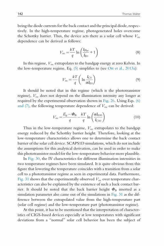
being the diode currents for the back contact and the principal diode, respec-
tively. In the high-temperature regime, photogenerated holes overcome
the Schottky barrier. Thus, the device acts there as a solar cell whose Voc
dependence can be derived as follows:
Voc¼ kT
qln
IPhe
IE0+ 1
� �(8)
In this regime, Voc extrapolates to the bandgap energy at zero Kelvin. In
the low-temperature regime, Eq. (5) simplifies to (see Ott et al., 2013a):
Voc¼ kT
qln
IC0
αIE0
� �(9)
It should be noted that in this regime (which is the phototransistor
regime), Voc does not depend on the illumination intensity any longer as
required by the experimental observation shown in Fig. 26. Using Eqs. (6)
and (7), the following temperature dependence of Voc can be derived:
Voc¼Eg�ΦB
q�kT
qln
αIE00IC00
� �(10)
Thus in the low-temperature regime, Voc extrapolates to the bandgap
energy reduced by the Schottky barrier height. Therefore, looking at the
low-temperature characteristics allows one to determine the back contact
barrier of the solar cell device. SCAPS1D simulations, which do not include
the assumptions for this analytical derivation, can be used in order to make
this phototransistor model for the low-temperature behavior more plausible.
In Fig. 30, the IV characteristics for different illumination intensities in
two temperature regimes have been simulated. It is quite obvious from this
figure that lowering the temperature coincides with a transition from a solar
cell to a phototransistor regime as seen in experimental data. Furthermore,
Fig. 31 shows that the experimentally observed Voc over temperature char-
acteristics can also be explained by the existence of such a back contact bar-
rier. It should be noted that the back barrier height ΦB inserted as a
simulation parameter also came out of the simulations in Fig. 31 as the dif-
ference between the extrapolated value from the high-temperature part
(solar cell regime) and the low-temperature part (phototransistor regime).
At this point, it has to be mentioned that the interpretation of character-
istics of CIGS-based devices especially at low temperatures with significant
deviations from a “normal” solar cell behavior has been the subject of
142 Thomas Walter
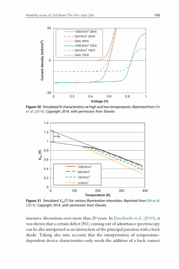
intensive discussions over more than 20 years. In Eisenbarth et al. (2010), it
was shown that a certain defect (N1) coming out of admittance spectroscopy
can be also interpreted as an interaction of the principal junction with a back
diode. Taking also into account that the interpretation of temperature-
dependent device characteristics only needs the addition of a back contact
0
0.2
0.4
0.6
0.8
1
1.2
1.4
0 100 200 300 400
Vo
c (
V)
Temperature (K)
1000 W/m2
500 W/m2
100 W/m2
10 W/m2
fB
Figure 31 Simulated Voc(T) for various illumination intensities. Reprinted from Ott et al.(2014). Copyright 2014, with permission from Elsevier.
-50
0
50
0 0.2 0.4 0.6 0.8 1
Cu
rren
t d
en
sit
y (
mA
/cm
2)
Voltage (V)
1000 W/m2 300 K
500 W/m2 300 K
Dark 300 K
1000 W/m2 150 K
500 W/m2 150 K
Dark 150 K
Figure 30 Simulated IV characteristics at high and low temperatures. Reprinted from Ottet al. (2014). Copyright 2014, with permission from Elsevier.
143Reliability Issues of CIGS-Based Thin Film Solar Cells
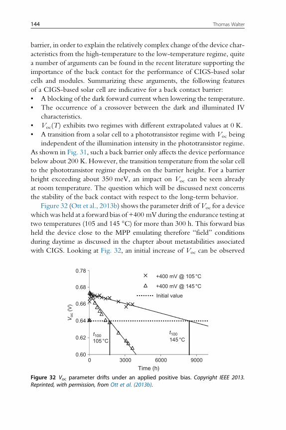
barrier, in order to explain the relatively complex change of the device char-
acteristics from the high-temperature to the low-temperature regime, quite
a number of arguments can be found in the recent literature supporting the
importance of the back contact for the performance of CIGS-based solar
cells and modules. Summarizing these arguments, the following features
of a CIGS-based solar cell are indicative for a back contact barrier:
• A blocking of the dark forward current when lowering the temperature.
• The occurrence of a crossover between the dark and illuminated IV
characteristics.
• Voc(T) exhibits two regimes with different extrapolated values at 0 K.
• A transition from a solar cell to a phototransistor regime with Voc being
independent of the illumination intensity in the phototransistor regime.
As shown in Fig. 31, such a back barrier only affects the device performance
below about 200 K. However, the transition temperature from the solar cell
to the phototransistor regime depends on the barrier height. For a barrier
height exceeding about 350 meV, an impact on Voc can be seen already
at room temperature. The question which will be discussed next concerns
the stability of the back contact with respect to the long-term behavior.
Figure 32 (Ott et al., 2013b) shows the parameter drift ofVoc for a device
which was held at a forward bias of +400 mV during the endurance testing at
two temperatures (105 and 145 °C) for more than 300 h. This forward bias
held the device close to the MPP emulating therefore “field” conditions
during daytime as discussed in the chapter about metastabilities associated
with CIGS. Looking at Fig. 32, an initial increase of Voc can be observed
3000
105 °Ct100
145 °Ct100
00.60
0.62
0.64Voc
(V
) 0.66
0.68
0.78
6000
Time (h)
9000
Initial value
+400 mV @ 105 °C
+400 mV @ 145 °C
Figure 32 Voc parameter drifts under an applied positive bias. Copyright IEEE 2013.Reprinted, with permission, from Ott et al. (2013b).
144 Thomas Walter
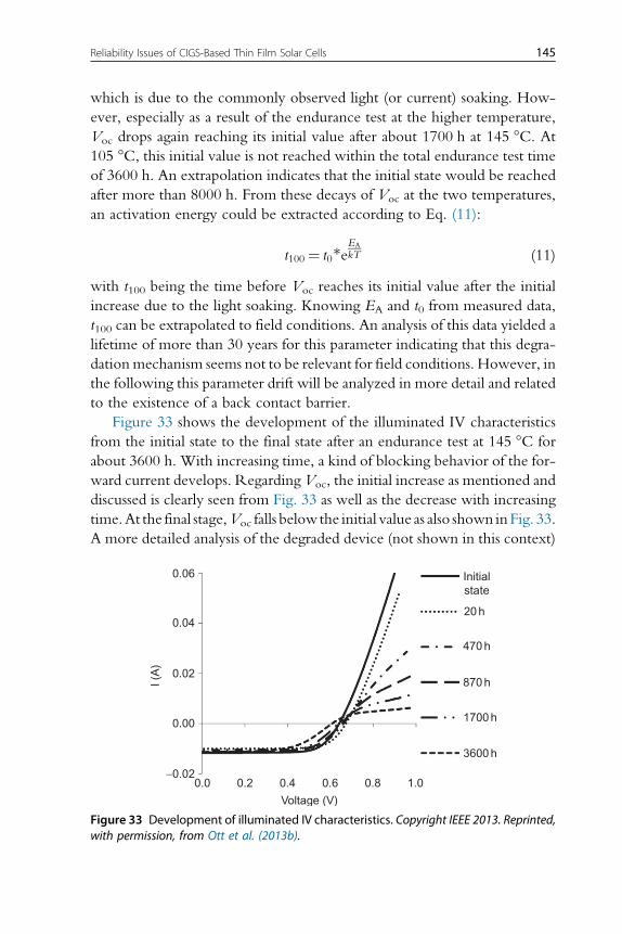
which is due to the commonly observed light (or current) soaking. How-
ever, especially as a result of the endurance test at the higher temperature,
Voc drops again reaching its initial value after about 1700 h at 145 °C. At105 °C, this initial value is not reached within the total endurance test time
of 3600 h. An extrapolation indicates that the initial state would be reached
after more than 8000 h. From these decays of Voc at the two temperatures,
an activation energy could be extracted according to Eq. (11):
t100¼ t0*eEA
kT (11)
with t100 being the time before Voc reaches its initial value after the initial
increase due to the light soaking. Knowing EA and t0 from measured data,
t100 can be extrapolated to field conditions. An analysis of this data yielded a
lifetime of more than 30 years for this parameter indicating that this degra-
dationmechanism seems not to be relevant for field conditions. However, in
the following this parameter drift will be analyzed in more detail and related
to the existence of a back contact barrier.
Figure 33 shows the development of the illuminated IV characteristics
from the initial state to the final state after an endurance test at 145 °C for
about 3600 h. With increasing time, a kind of blocking behavior of the for-
ward current develops. RegardingVoc, the initial increase as mentioned and
discussed is clearly seen from Fig. 33 as well as the decrease with increasing
time.At the final stage,Voc falls below the initial value as also shown inFig. 33.
A more detailed analysis of the degraded device (not shown in this context)
0.0−0.02
0.00
0.02
I (A
)
0.04
0.06
0.2 0.4 0.6
Voltage (V)
0.8 1.0
3600 h
1700 h
870 h
470 h
20 h
Initialstate
Figure 33 Development of illuminated IV characteristics. Copyright IEEE 2013. Reprinted,with permission, from Ott et al. (2013b).
145Reliability Issues of CIGS-Based Thin Film Solar Cells
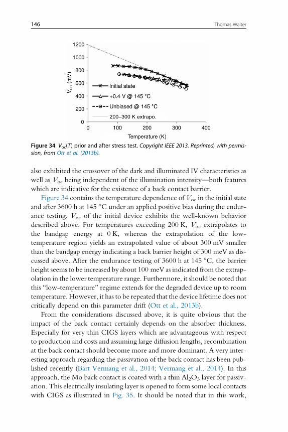
also exhibited the crossover of the dark and illuminated IV characteristics as
well as Voc being independent of the illumination intensity—both features
which are indicative for the existence of a back contact barrier.
Figure 34 contains the temperature dependence of Voc in the initial state
and after 3600 h at 145 °C under an applied positive bias during the endur-
ance testing. Voc of the initial device exhibits the well-known behavior
described above. For temperatures exceeding 200 K, Voc extrapolates to
the bandgap energy at 0 K, whereas the extrapolation of the low-
temperature region yields an extrapolated value of about 300 mV smaller
than the bandgap energy indicating a back barrier height of 300 meV as dis-
cussed above. After the endurance testing of 3600 h at 145 °C, the barrierheight seems to be increased by about 100 meV as indicated from the extrap-
olation in the lower temperature range. Furthermore, it should be noted that
this “low-temperature” regime extends for the degraded device up to room
temperature. However, it has to be repeated that the device lifetime does not
critically depend on this parameter drift (Ott et al., 2013b).
From the considerations discussed above, it is quite obvious that the
impact of the back contact certainly depends on the absorber thickness.
Especially for very thin CIGS layers which are advantageous with respect
to production and costs and assuming large diffusion lengths, recombination
at the back contact should become more and more dominant. A very inter-
esting approach regarding the passivation of the back contact has been pub-
lished recently (Bart Vermang et al., 2014; Vermang et al., 2014). In this
approach, the Mo back contact is coated with a thin Al2O3 layer for passiv-
ation. This electrically insulating layer is opened to form some local contacts
with CIGS as illustrated in Fig. 35. It should be noted that in this work,
Figure 34 Voc(T) prior and after stress test. Copyright IEEE 2013. Reprinted, with permis-sion, from Ott et al. (2013b).
146 Thomas Walter

absorber thicknesses below 500 nm were used which is about one quarter of
the usual thickness. Figure 36 compares the passivated with the unpassivated
back contact regarding the device performance. From that diagram, it is
quite obvious that a passivated back contact both improves Voc and jscdue to reduced recombination. The impact of such a back contact passiv-
ation on the Schottky barrier has not been investigated so far. This very
interesting work is still in a research state. Possible implementations in a
production line have not been considered so far.
Conclusions on Back ContactEspecially, highly efficient but thin devices with a long diffusion length
require increased attention with respect to the back contact. Certain
Figure 35 Ultrathin CIGS-based solar cell with point contacts. Copyright IEEE 2014.Reprinted, with permission, from Vermang et al. (2014).
0−30
−20
−10
0Rs = 0.65 Ωcm2; Gsh = 1.6 mS/cm2
Rs = 0.65 Ωcm2; Gsh = 2.6 mS/cm2
J0 = 3.7 × 10⁻⁸ mA/cm2; n = 1.3;
J0 = 8.8 × 10⁻⁸ mA/cm2; n = 1.6;
Unpassivated reference cell
AI2O3 rear passivated cell
J (m
A/c
m2 )
10
20
30
100 200 300 400
V (mV)
500 600 700 800
Figure 36 Illuminated IV characteristics showing the impact of back contact passiv-ation. Copyright IEEE 2014. Reprinted, with permission, from Vermang et al. (2014).
147Reliability Issues of CIGS-Based Thin Film Solar Cells
characteristics which may arise as a consequence of accelerated aging can be
interpreted in terms of a “phototransistor” as a consequence of a back con-
tact diode. Ongoing research seeks to provide measures to passivate the back
contact allowing extremely thin layers with associated high efficiencies.
With respect to these extremely thin layers, the impact of a Schottky barrier
at the back contact should be taken into consideration and investigated.
REFERENCESBart Vermang, V.F., Gao, X., Edoff, M., 2014. Improved rear surface passivation of Cu(In,
Ga)Se2 solar cells: a combination of an Al2O3 rear surface passivation layer and nanosizedlocal rear point contacts. IEEE J. Photovolt. 4 (1), 486–492.
Bl€osch, P., Nishiwaki, S., Chirila, A., Kranz, L., Fella, C., Pianezzi, F., Adelhelm, C.,Franzke, E., Buecheler, S., Tiwari, A., 2013. Sodium-doped molybdenum back contactsfor flexible Cu(In, Ga)Se2 solar cells. Thin Solid Films 535, 214–219.
Boone, T., Soltz, D., Kinkhabwala, A., Zapalac, G., Pinarbasi, M., 2012. Optoelectronicmethods for characterizing uniformity in CIGS thin film solar cells. In: Proc. 38th IEEEPVSC, Seattle, pp. 1732–1735.
Borowski, P., Karg, F., 2014. PID-free CIGS thin film modules. In: Proc. 29th EU PVSEC,Amsterdam, pp. 2356–2362.
Chirila, A., Reinhard, P., 2013. Potassium-induced surface modification of Cu(In, Ga)Se2thin films for high-efficiency solar cells. Nat. Mater. 12, 1107–1111.
Dongaonkar, S., Sheets, E., Agrawal, R., Alam, M., 2012. Reverse stress metastability ofshunt current in CIGS solar cells. In: Proc. 38th IEEE PVSC, pp. 868–872.
Dongaonkar, S., Deline, C., Alam, M., 2013. Performance and reliability implications oftwo-dimensional shading in monolithic thin-film photovoltaic modules. IEEE J. Photo-volt. 3 (4), 1367–1375.
Eisenbarth, T., Caballero, R., Nichterwitz, M., Kaufmann, C., Schock, H.W., Unold, T.,2010. Interpretation of admittance, capacitance-voltage, and current–voltage signaturesin Cu(In,Ga)Se2 thin film solar cells. J. Appl. Phys. 107, 034509.
Fjallstrom, V., Salome, P., Hultqvist, A., Edoff, M., Jarmar, T., Aitken, B., Zhang, K.,Fuller, K., Williams, C., 2013. Potential-induced degradation of CuIn1-xGaxSe2 thinfilm solar cells. IEEE J. Photovolt. 3 (3), 1090–1094.
Hoffmann, S., Koehl, M., 2012. Modeling the leakage current for potential induced degra-dation. In: Proc. 28th EUPVSEC, Frankfurt, pp. 3336–3339.
Igalson, M., Urbaniak, A., Macielak, K., Tomassini, M., Barreau, N., Spiering, S., 2011. Bar-riers for current transport in CIGS structures. In: Proc. 37th IEEE PVSC, Seattle,pp. 2727–2731.
Igalson, M., Urbaniak, A., Zabierowski, P., Maksoud, H., Buffiere, M., Barreau, N.,Spiering, S., 2013. Red-blue effect in Cu(In, Ga)Se2-based devices revisited. Thin SolidFilms 535, 302–306.
Janssen, G., Sloof, L., Bende, E., 2012. 2D-finite element model of a CIGSmodule. In: Proc.27th EU PVSEC, Frankfurt, pp. 2368–2371.
Kempa, H., Rissom, T., Hlawatsch, U., Gaudig, M., Obereigner, F., Kaufmann, C.,Scheer, R., 2013. Metastability of solar cells based on evaporated chalcopyrite absorberlayers prepared with varying selenium flux. Thin Solid Films 535, 340–342.
K€otschau, I.M., Turcu, M., Rau, U., Schock, H.W., 2001. Structural and electronicproperties of polycrystalline Cu(In,Ga)(S,Se)2 alloys. In: Mat. Res. Soc. Symp.Proc. 668.
148 Thomas Walter
Lany, S., Zunger, A., 2006. Light- and bias induced metastabilities in Cu(In, Ga)Se2 basedsolar cells caused by the (VSe-VCu) vacancy complex. J. Appl. Phys. 100, 113725.
Lany, S., Zunger, A., 2008. Intrinsic DX centers in ternary chalcopyrite semiconductors.Phys. Rev. Lett. 100, 016401.
Lechner, P., Hummel, S., Geyer, D., Mohring, H.-D., 2013. PID-behaviour of thin-film-and c-Si PV-modules. In: Proc. 27th EU PVSEC, Paris, pp. 2810–2815.
Lee, S., Koo, J., Kim, S., Cheon, T., Oh, J., Kim, S., Kim, W., 2013. Characteristics ofMoSe2 formation during rapid thermal processing of Mo-coated glass. Thin Solid Films535, 206–213.
Mack, P., Walter, T., Kniese, R., Hariskos, D., Schaffler, R., 2008. Reverse bias and reversecurrents in CIGS thin film solar cells and modules. In: Proc. 23rd EU PVSEC, Valencia.
Mack, P., Walter, T., Hariskos, D., Schaffler, R., Dimmler, B., 2009. Endurance testing andaccelerated ageing of CIGS thin film solar cells. In: Proc. 24th EU PVSEC, Hamburg,pp. 2439–2442.
Mack, P., Ott, T., Schwable, F., Runai, F., Walter, T., 2010. 2D-network simulation andmodelling of CIGS modules. In: Proc. 25th EU PVSEC, Valencia.
Moore, J., Dogaonkar, S., Vamsi, R., Chavali, K., Alam, M., Lundstrom, M., 2014. Cor-relation of built-in potential and I–V crossover in thin-film solar cells. IEEE J. Photovolt.4 (4), 1138–1148.
Noufi, R., Zweibel, K., 2006. High-efficiency CdTe and CIGS thin-film solar cells: high-lights and challenges. In: Proc. 4th World Conf. Photovolt. Energy Convers. vol. 1,pp. 317–320.
Ott, T., Mack, P., Trudel, F., Schulz, Y., Walter, T., 2011. Accelerated ageingand luminescence of CIGS solar cells. In: Proc. 26th EU PVSEC, Hamburg,pp. 2421–2424.
Ott, T., Runai, F., Schwable, F.,Walter, T., 2012. 2D network simulation and luminescencecharacterization of CIGS thin film modules. Prog. Photovolt. Res. Appl. 20 (5),600–605.
Ott, T., Walter, T., Unold, T., 2013a. Phototransistor effects in Cu(In, Ga)Se2 solar cells.Thin Solid Films 535, 275–278.
Ott, T., Walter, T., Hariskos, D., Kiowski, O., Schaffler, R., 2013b. Accelerated aging andcontact degradation of CIGS solar cells. IEEE J. Photovolt. 3 (1), 514–519.
Ott, T., Sch€onberger, F., Walter, T., Hariskos, D., Kiowski, O., Salomon, O., Schaffler, R.,2014. Verification of phototransistor model for Cu(In,Ga)Se2 solar cells. Thin SolidFilms 582, 392–396.
Pingel, S., Frank, O., Winkler, M., Daryan, S., Geipel, T., Hoehne, H., Berghold, J., 2010.Potential induced degradation of solar cells and panels. In: Proc. 35th IEEE PVSC,pp. 2817–2822.
Runai, F., Schwable, F., Walter, T., Fidler, A., Gorse, S., Hahn, T., K€otschau, I., 2011.Imaging and performance of CIGS thin film modules. In: Proc. 37th IEEE PVSC,Seattle, pp. 3399–3403.
Salome, P., Fjallstr€om, V., Hultqvist, A., Edoff, M., 2014. Incorporation of Na in Cu(In, Ga)Se2 thin-film solar cells: a statistical comparison between Na from soda-lime glass andfrom a precursor layer of NaF. IEEE J. Photovolt. 4 (6), 1659–1664.
Sites, J., 2010. Thin-film photovoltaics: what are the reliability issues and where do theyoccur? In: Proc. Reliab. Phys. Symp., Anaheim, pp. 494–498.
Szaniawski, P., Lindahl, J., T€orndahl, T., Zimmermann,U., Edoff,M., 2013. Light-enhancedreverse breakdown in Cu(In, Ga)Se2 solar cells. Thin Solid Films 535, 326–330.
Sze, S.M., 1981. Physics of Semiconductor Devices. Wiley & Sons Inc., New York,Chichester, Brisbane, Toronto, Singapore.
Tran, T.M.H., Pieters, B.E., Siegloch, M., Gerber, A., Ulbrich, C., Kirchartz, T.,Schaffler, R., Rau, U., 2011. Characterization of shunts in Cu(In, Ga)Se2 solar modules
149Reliability Issues of CIGS-Based Thin Film Solar Cells

via combined electroluminescence and dark lock-in thermography analysis. In: Proc.26th EU PVSEC, Hamburg, pp. 2981–2985.
Vermang, B., Watjen, J.T., Frisk, C., Fjallstr€om, V., Rostvall, F., Edoff, M., Salome, P.,Borme, J., Nicoara, N., Sadewasser, S., 2014. Introduction of Si PERC rear contactingdesign to boost efficiency of Cu(In, Ga)Se2 solar cells. IEEE J. Photovolt. 4 (6),1644–1649.
Wada, T., Kohara, N., Nishiwaki, N., Negami, T., 2001. Characterization of the Cu(In, Ga)Se2/Mo interface in CIGS solar cells. Thin Solid Films 387, 118–122.
Wendlandt, S., Giese, A., Drobisch, A., Tornow, D., Hanusch, M., Berghold, J., Krauter, S.,Grunow, P., 2012. The temperature as the real hot spot risk factor at PV-modules.In: Proc. 27th EU PVSEC, Frankfurt, pp. 3553–3557.
Westin, P.-O., Zimmermann, U., Stolt, L., Edoff, M., 2009. Reverse bias damage in CIGSmodules. In: Proc. 24th EU PVSEC, Hamburg, pp. 2967–2970.
150 Thomas Walter
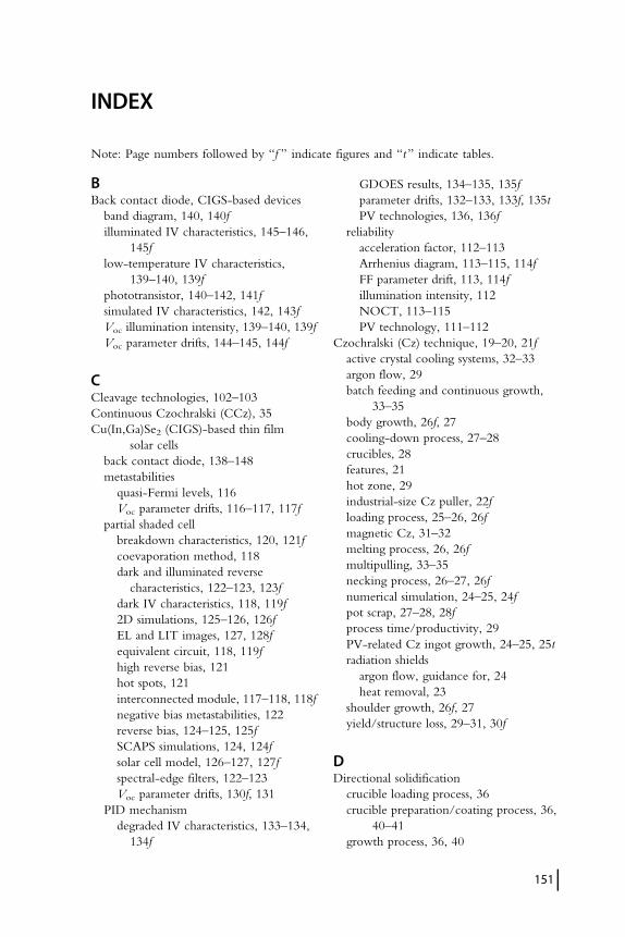
INDEX
Note: Page numbers followed by “f ” indicate figures and “t” indicate tables.
BBack contact diode, CIGS-based devices
band diagram, 140, 140f
illuminated IV characteristics, 145–146,
145f
low-temperature IV characteristics,
139–140, 139f
phototransistor, 140–142, 141f
simulated IV characteristics, 142, 143f
Voc illumination intensity, 139–140, 139f
Voc parameter drifts, 144–145, 144f
CCleavage technologies, 102–103
Continuous Czochralski (CCz), 35
Cu(In,Ga)Se2 (CIGS)-based thin film
solar cells
back contact diode, 138–148
metastabilities
quasi-Fermi levels, 116
Voc parameter drifts, 116–117, 117f
partial shaded cell
breakdown characteristics, 120, 121f
coevaporation method, 118
dark and illuminated reverse
characteristics, 122–123, 123f
dark IV characteristics, 118, 119f
2D simulations, 125–126, 126f
EL and LIT images, 127, 128f
equivalent circuit, 118, 119f
high reverse bias, 121
hot spots, 121
interconnected module, 117–118, 118f
negative bias metastabilities, 122
reverse bias, 124–125, 125f
SCAPS simulations, 124, 124f
solar cell model, 126–127, 127f
spectral-edge filters, 122–123
Voc parameter drifts, 130f, 131
PID mechanism
degraded IV characteristics, 133–134,
134f
GDOES results, 134–135, 135f
parameter drifts, 132–133, 133f, 135t
PV technologies, 136, 136f
reliability
acceleration factor, 112–113
Arrhenius diagram, 113–115, 114f
FF parameter drift, 113, 114f
illumination intensity, 112
NOCT, 113–115
PV technology, 111–112
Czochralski (Cz) technique, 19–20, 21f
active crystal cooling systems, 32–33
argon flow, 29
batch feeding and continuous growth,
33–35
body growth, 26f, 27
cooling-down process, 27–28
crucibles, 28
features, 21
hot zone, 29
industrial-size Cz puller, 22f
loading process, 25–26, 26f
magnetic Cz, 31–32
melting process, 26, 26f
multipulling, 33–35
necking process, 26–27, 26f
numerical simulation, 24–25, 24f
pot scrap, 27–28, 28f
process time/productivity, 29
PV-related Cz ingot growth, 24–25, 25t
radiation shields
argon flow, guidance for, 24
heat removal, 23
shoulder growth, 26f, 27
yield/structure loss, 29–31, 30f
DDirectional solidification
crucible loading process, 36
crucible preparation/coating process, 36,
40–41
growth process, 36, 40
151
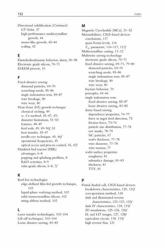
Directional solidification (Continued )
GT-Solar, 37
high-performance multicrystalline
growth, 44
mono-like growth, 42–44
scaling, 42
EElastohydrodynamic behavior, slurry, 96–98
Electronic grade silicon, 70–71
ELKEM process, 10
FFixed abrasive sawing
diamond particles, 69–70
scratching mode, 85–86
single indentation tests, 85–87
wire breakage, 80
wire wear, 80
Float-Zone (FZ) growth technique
chemical etching, 49
vs. Cz method, 45–47, 47t
diameter limitations, 51–53
features, 48–49
feed rods, 49, 49–50f, 53
heat transfer, 45–47
needle-eye technique, 45, 46f
operational frequencies, 45
optical access and process control, 45, 47f
Fluidized bed reactor (FBR)
advantages, 6–8
popping and splashing problem, 8
R&D activities, 8–9
solar-grade silicon, 6–8, 7f
KKerf-less technologies
edge-defined film-fed growth technique,
102
liquid-phase wafering method, 102
solid monocrystalline silicon, 102
string ribbon method, 102
LLayer transfer technologies, 103–104
Lift-off techniques, 103–104
Loose abrasive sawing, 83–85
MMagnetic Czochralski (MCz), 31–32
Metastabilities, CIGS-based devices
conclusions, 117
quasi-Fermi levels, 116
Voc parameter, 116–117, 117f
Multicrystalline casting, 11–12
Multiwire sawing technology
electronic grade silicon, 70–71
fixed abrasive sawing, 69–71, 79–80
diamond particles, 69–70
scratching mode, 85–86
single indentation tests, 85–87
wire breakage, 80
wire wear, 80
fracture behavior, 70
principles, 65–66
single indentation tests
fixed abrasive sawing, 85–87
loose abrasive sawing, 83–85
slurry-based sawing
dependence properties, 74–77
force in ingot feed direction, 72
friction force, 73–74
particle size distribution, 77–78
saw marks, 78–79
SiC particles, 67
wafer thickness, 77–78
wire diameter, 77–78
wire tension, 77
wafer surface properties
roughness, 81
subsurface damage, 81–83
thickness, 81
TTV, 81
PPartial shaded cell, CIGS-based devices
breakdown characteristics, 120, 121f
coevaporation method, 118
dark and illuminated reverse
characteristics, 122–123, 123f
dark IV characteristics, 118, 119f
2D simulations, 125–126, 126f
EL and LIT images, 127, 128f
equivalent circuit, 118, 119f
high reverse bias, 121
152 Index
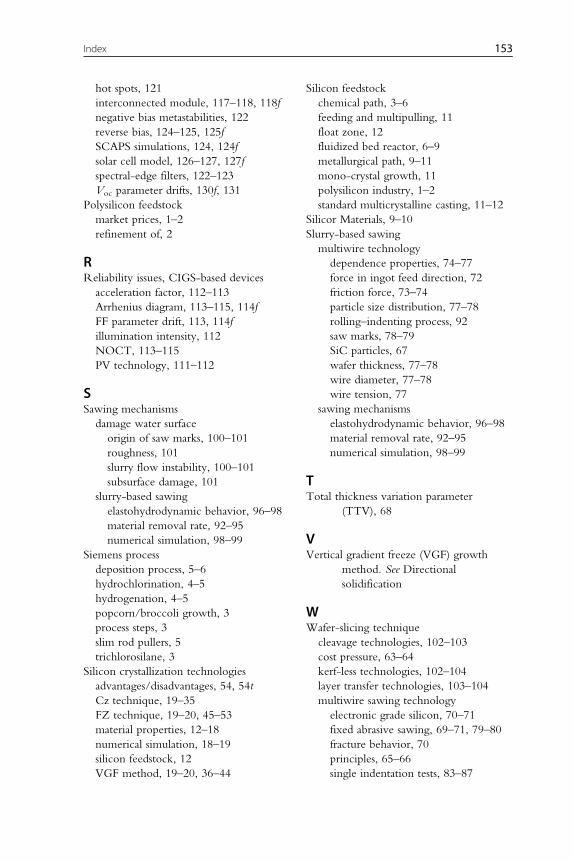
hot spots, 121
interconnected module, 117–118, 118f
negative bias metastabilities, 122
reverse bias, 124–125, 125f
SCAPS simulations, 124, 124f
solar cell model, 126–127, 127f
spectral-edge filters, 122–123
Voc parameter drifts, 130f, 131
Polysilicon feedstock
market prices, 1–2
refinement of, 2
RReliability issues, CIGS-based devices
acceleration factor, 112–113
Arrhenius diagram, 113–115, 114f
FF parameter drift, 113, 114f
illumination intensity, 112
NOCT, 113–115
PV technology, 111–112
SSawing mechanisms
damage water surface
origin of saw marks, 100–101
roughness, 101
slurry flow instability, 100–101
subsurface damage, 101
slurry-based sawing
elastohydrodynamic behavior, 96–98
material removal rate, 92–95
numerical simulation, 98–99
Siemens process
deposition process, 5–6
hydrochlorination, 4–5
hydrogenation, 4–5
popcorn/broccoli growth, 3
process steps, 3
slim rod pullers, 5
trichlorosilane, 3
Silicon crystallization technologies
advantages/disadvantages, 54, 54t
Cz technique, 19–35
FZ technique, 19–20, 45–53
material properties, 12–18
numerical simulation, 18–19
silicon feedstock, 12
VGF method, 19–20, 36–44
Silicon feedstock
chemical path, 3–6
feeding and multipulling, 11
float zone, 12
fluidized bed reactor, 6–9
metallurgical path, 9–11
mono-crystal growth, 11
polysilicon industry, 1–2
standard multicrystalline casting, 11–12
Silicor Materials, 9–10
Slurry-based sawing
multiwire technology
dependence properties, 74–77
force in ingot feed direction, 72
friction force, 73–74
particle size distribution, 77–78
rolling–indenting process, 92
saw marks, 78–79
SiC particles, 67
wafer thickness, 77–78
wire diameter, 77–78
wire tension, 77
sawing mechanisms
elastohydrodynamic behavior, 96–98
material removal rate, 92–95
numerical simulation, 98–99
TTotal thickness variation parameter
(TTV), 68
VVertical gradient freeze (VGF) growth
method. See Directional
solidification
WWafer-slicing technique
cleavage technologies, 102–103
cost pressure, 63–64
kerf-less technologies, 102–104
layer transfer technologies, 103–104
multiwire sawing technology
electronic grade silicon, 70–71
fixed abrasive sawing, 69–71, 79–80
fracture behavior, 70
principles, 65–66
single indentation tests, 83–87
153Index

Wafer-slicing technique (Continued )
slurry-based sawing, 66–68, 72–79
photovoltaic market, 64
sawing mechanisms
slurry-based sawing, 90–99
water surface properties, 99–101
Wire tension, 77
154 Index
CONTENTS OF VOLUMES IN THIS SERIES
Volume 1 Physics of III–V Compounds
C. Hilsum, Some Key Features of III–V Compounds
F. Bassani, Methods of Band Calculations Applicable to III–V Compounds
E. O. Kane, The k-p Method
V. L. Bonch–Bruevich, Effect of Heavy Doping on the Semiconductor Band Structure
D. Long, Energy Band Structures of Mixed Crystals of III–V Compounds
L. M. Roth and P. N. Argyres, Magnetic Quantum Effects
S. M. Puri and T. H. Geballe, Thermomagnetic Effects in the Quantum Region
W. M. Becker, Band Characteristics near Principal Minima from Magnetoresistance
E. H. Putley, Freeze-Out Effects, Hot Electron Effects, and Submillimeter Photoconductivity in InSb
H. Weiss, Magnetoresistance
B. Ancker-Johnson, Plasma in Semiconductors and Semimetals
Volume 2 Physics of III–V Compounds
M. G. Holland, Thermal Conductivity
S. I. Novkova, Thermal Expansion
U. Piesbergen, Heat Capacity and Debye Temperatures
G. Giesecke, Lattice Constants
J. R. Drabble, Elastic Properties
A. U. Mac Rae and G. W. Gobeli, Low Energy Electron Diffraction Studies
R. Lee Mieher, Nuclear Magnetic Resonance
B. Goldstein, Electron Paramagnetic Resonance
T. S. Moss, Photoconduction in III–V Compounds
E. Antoncik and J. Tauc, Quantum Efficiency of the Internal Photoelectric Effect in InSb
G. W. Gobeli and I. G. Allen, Photoelectric Threshold and Work Function
P. S. Pershan, Nonlinear Optics in III–V Compounds
M. Gershenzon, Radiative Recombination in the III–V Compounds
F. Stern, Stimulated Emission in Semiconductors
Volume 3 Optical Properties of III–V Compounds
M. Hass, Lattice Reflection
W. G. Spitzer, Multiphonon Lattice Absorption
D. L. Stierwalt and R. F. Potter, Emittance Studies
H. R. Philipp and H. Ehrenveich, Ultraviolet Optical Properties
M. Cardona, Optical Absorption Above the Fundamental Edge
E. J. Johnson, Absorption Near the Fundamental Edge
J. O. Dimmock, Introduction to the Theory of Exciton States in Semiconductors
155
B. Lax and J. G. Mavroides, Interband Magnetooptical Effects
H. Y. Fan, Effects of Free Carries on Optical Properties
E. D. Palik and G. B. Wright, Free-Carrier Magnetooptical Effects
R. H. Bube, Photoelectronic Analysis
B. O. Seraphin and H. E. Benett, Optical Constants
Volume 4 Physics of III–V Compounds
N. A. Goryunova, A. S. Borchevskii and D. N. Tretiakov, Hardness
N. N. Sirota, Heats of Formation and Temperatures and Heats of Fusion of Compounds of AIIIBV
D. L. Kendall, Diffusion
A. G. Chynoweth, Charge Multiplication Phenomena
R. W. Keyes, The Effects of Hydrostatic Pressure on the Properties of III–V Semiconductors
L. W. Aukerman, Radiation Effects
N. A. Goryunova, F. P. Kesamanly, and D. N. Nasledov, Phenomena in Solid Solutions
R. T. Bate, Electrical Properties of Nonuniform Crystals
Volume 5 Infrared Detectors
H. Levinstein, Characterization of Infrared Detectors
P. W. Kruse, Indium Antimonide Photoconductive and Photoelectromagnetic Detectors
M. B. Prince, Narrowband Self-Filtering Detectors
I. Melngalis and T. C. Hannan, Single-Crystal Lead-Tin Chalcogenides
D. Long and J. L. Schmidt, Mercury-Cadmium Telluride and Closely Related Alloys
E. H. Putley, The Pyroelectric Detector
N. B. Stevens, Radiation Thermopiles
R. J. Keyes and T. M. Quist, Low Level Coherent and Incoherent Detection in the Infrared
M. C. Teich, Coherent Detection in the Infrared
F. R. Arams, E. W. Sard, B. J. Peyton and F. P. Pace, Infrared Heterodyne Detection with Gigahertz IF
Response
H. S. Sommers, Jr., Macrowave-Based Photoconductive Detector
R. Sehr and R. Zuleeg, Imaging and Display
Volume 6 Injection Phenomena
M. A. Lampert and R. B. Schilling, Current Injection in Solids: The Regional Approximation Method
R. Williams, Injection by Internal Photoemission
A. M. Barnett, Current Filament Formation
R. Baron and J. W. Mayer, Double Injection in Semiconductors
W. Ruppel, The Photoconductor-Metal Contact
156 Contents of Volumes in this Series
Volume 7 Application and Devices
Part A
J. A. Copeland and S. Knight, Applications Utilizing Bulk Negative Resistance
F. A. Padovani, The Voltage-Current Characteristics of Metal-Semiconductor Contacts
P. L. Hower, W. W. Hooper, B. R. Cairns, R. D. Fairman, and D. A. Tremere, The GaAs Field-Effect
Transistor
M. H. White, MOS Transistors
G. R. Antell, Gallium Arsenide Transistors
T. L. Tansley, Heterojunction Properties
Part B
T. Misawa, IMPATT Diodes
H. C. Okean, Tunnel Diodes
R. B. Campbell and Hung-Chi Chang, Silicon Junction Carbide Devices
R. E. Enstrom, H. Kressel, and L. Krassner, High-Temperature Power Rectifiers of GaAs1�xPx
Volume 8 Transport and Optical Phenomena
R. J. Stirn, Band Structure and Galvanomagnetic Effects in III–V Compounds with Indirect Band Gaps
R. W. Ure, Jr., Thermoelectric Effects in III–V Compounds
H. Piller, Faraday Rotation
H. Barry Bebb and E. W. Williams, Photoluminescence I: Theory
E. W. Williams and H. Barry Bebb, Photoluminescence II: Gallium Arsenide
Volume 9 Modulation Techniques
B. O. Seraphin, Electroreflectance
R. L. Aggarwal, Modulated Interband Magnetooptics
D. F. Blossey and Paul Handler, Electroabsorption
B. Batz, Thermal and Wavelength Modulation Spectroscopy
I. Balslev, Piezooptical Effects
D. E. Aspnes and N. Bottka, Electric-Field Effects on the Dielectric Function of Semiconductors and
Insulators
Volume 10 Transport Phenomena
R. L. Rhode, Low-Field Electron Transport
J. D. Wiley, Mobility of Holes in III–V Compounds
C. M. Wolfe and G. E. Stillman, Apparent Mobility Enhancement in Inhomogeneous Crystals
R. L. Petersen, The Magnetophonon Effect
157Contents of Volumes in this Series
Volume 11 Solar Cells
H. J. Hovel, Introduction; Carrier Collection, Spectral Response, and Photocurrent; Solar Cell Electrical
Characteristics; Efficiency; Thickness; Other Solar Cell Devices; Radiation Effects; Temperature
and Intensity; Solar Cell Technology
Volume 12 Infrared Detectors (II)
W. L. Eiseman, J. D. Merriam, and R. F. Potter, Operational Characteristics of Infrared Photodetectors
P. R. Bratt, Impurity Germanium and Silicon Infrared Detectors
E. H. Putley, InSb Submillimeter Photoconductive Detectors
G. E. Stillman, C. M. Wolfe, and J. O. Dimmock, Far-Infrared Photoconductivity in High Purity GaAs
G. E. Stillman and C. M. Wolfe, Avalanche Photodiodes
P. L. Richards, The Josephson Junction as a Detector of Microwave and Far-Infrared Radiation
E. H. Putley, The Pyroelectric Detector – An Update
Volume 13 Cadmium Telluride
K. Zanio, Materials Preparations; Physics; Defects; Applications
Volume 14 Lasers, Junctions, Transport
N. Holonyak, Jr., and M. H. Lee, Photopumped III–V Semiconductor Lasers
H. Kressel and J. K. Butler, Heterojunction Laser Diodes
A. Van der Ziel, Space-Charge-Limited Solid-State Diodes
P. J. Price, Monte Carlo Calculation of Electron Transport in Solids
Volume 15 Contacts, Junctions, Emitters
B. L. Sharma, Ohmic Contacts to III–V Compounds Semiconductors
A. Nussbaum, The Theory of Semiconducting Junctions
J. S. Escher, NEA Semiconductor Photoemitters
Volume 16 Defects, (HgCd)Se, (HgCd)Te
H. Kressel, The Effect of Crystal Defects on Optoelectronic Devices
C. R.Whitsett, J. G. Broerman, and C. J. Summers, Crystal Growth and Properties of Hg1�xCdx Se Alloys
M. H. Weiler, Magnetooptical Properties of Hg1�x Cdx Te Alloys
P. W. Kruse and J. G. Ready, Nonlinear Optical Effects in Hg1�x Cdx Te
Volume 17 CW Processing of Silicon and Other Semiconductors
J. F. Gibbons, Beam Processing of Silicon
A. Lietoila, R. B. Gold, J. F. Gibbons, and L. A. Christel, Temperature Distributions and Solid Phase
Reaction Rates Produced by Scanning CW Beams
158 Contents of Volumes in this Series
A. Leitoila and J. F. Gibbons, Applications of CW Beam Processing to Ion Implanted Crystalline Silicon
N. M. Johnson, Electronic Defects in CW Transient Thermal Processed Silicon
K. F. Lee, T. J. Stultz, and J. F. Gibbons, Beam Recrystallized Polycrystalline Silicon: Properties,
Applications, and Techniques
T. Shibata, A. Wakita, T. W. Sigmon and J. F. Gibbons, Metal-Silicon Reactions and Silicide
Y. I. Nissim and J. F. Gibbons, CW Beam Processing of Gallium Arsenide
Volume 18 Mercury Cadmium Telluride
P. W. Kruse, The Emergence of (Hg1�x Cdx) Te as a Modern Infrared Sensitive Material
H. E. Hirsch, S. C. Liang, and A. G. White, Preparation of High-Purity Cadmium, Mercury, and
Tellurium
W. F. H. Micklethwaite, The Crystal Growth of Cadmium Mercury Telluride
P. E. Petersen, Auger Recombination in Mercury Cadmium Telluride
R. M. Broudy and V. J. Mazurczyck, (HgCd) Te Photoconductive Detectors
M. B. Reine, A. K. Soad, and T. J. Tredwell, Photovoltaic Infrared Detectors
M. A. Kinch, Metal-Insulator-Semiconductor Infrared Detectors
Volume 19 Deep Levels, GaAs, Alloys, Photochemistry
G. F. Neumark and K. Kosai, Deep Levels in Wide Band-Gap III–V Semiconductors
D. C. Look, The Electrical and Photoelectronic Properties of Semi-Insulating GaAs
R. F. Brebrick, Ching-Hua Su, and Pok-Kai Liao, Associated SolutionModel for Ga-In-Sb and Hg-Cd-Te
Y. Ya. Gurevich and Y. V. Pleskon, Photoelectrochemistry of Semiconductors
Volume 20 Semi-Insulating GaAs
R. N. Thomas, H. M. Hobgood, G. W. Eldridge, D. L. Barrett, T. T. Braggins, L. B. Ta, and S. K. Wang,
High-Purity LEC Growth and Direct Implantation of GaAs for Monolithic Microwave Circuits
C. A. Stolte, Ion Implantation and Materials for GaAs Integrated Circuits
C. G. Kirkpatrick, R. T. Chen, D. E. Holmes, P. M. Asbeck, K. R. Elliott, R. D. Fairman, and J. R. Oliver,
LEC GaAs for Integrated Circuit Applications
J. S. Blakemore and S. Rahimi, Models for Mid-Gap Centers in Gallium Arsenide
Volume 21 Hydrogenated Amorphous Silicon
Part A
J. I. Pankove, Introduction
M. Hirose, Glow Discharge; Chemical Vapor Deposition
Y. Uchida, di Glow Discharge
T. D. Moustakas, Sputtering
I. Yamada, Ionized-Cluster Beam Deposition
B. A. Scott, Homogeneous Chemical Vapor Deposition
159Contents of Volumes in this Series
F. J. Kampas, Chemical Reactions in Plasma Deposition
P. A. Longeway, Plasma Kinetics
H. A. Weakliem, Diagnostics of Silane Glow Discharges Using Probes and Mass Spectroscopy
L. Gluttman, Relation between the Atomic and the Electronic Structures
A. Chenevas-Paule, Experiment Determination of Structure
S. Minomura, Pressure Effects on the Local Atomic Structure
D. Adler, Defects and Density of Localized States
Part B
J. I. Pankove, Introduction
G. D. Cody, The Optical Absorption Edge of a-Si: H
N. M. Amer and W. B. Jackson, Optical Properties of Defect States in a-Si: H
P. J. Zanzucchi, The Vibrational Spectra of a-Si: H
Y. Hamakawa, Electroreflectance and Electroabsorption
J. S. Lannin, Raman Scattering of Amorphous Si, Ge, and Their Alloys
R. A. Street, Luminescence in a-Si: H
R. S. Crandall, Photoconductivity
J. Tauc, Time-Resolved Spectroscopy of Electronic Relaxation Processes
P. E. Vanier, IR-Induced Quenching and Enhancement of Photoconductivity and Photoluminescence
H. Schade, Irradiation-Induced Metastable Effects
L. Ley, Photoelectron Emission Studies
Part C
J. I. Pankove, Introduction
J. D. Cohen, Density of States from Junction Measurements in Hydrogenated Amorphous Silicon
P. C. Taylor, Magnetic Resonance Measurements in a-Si: H
K. Morigaki, Optically Detected Magnetic Resonance
J. Dresner, Carrier Mobility in a-Si: H
T. Tiedje, Information About Band-Tail States from Time-of-Flight Experiments
A. R. Moore, Diffusion Length in Undoped a-S: H
W. Beyer and J. Overhof, Doping Effects in a-Si: H
H. Fritzche, Electronic Properties of Surfaces in a-Si: H
C. R. Wronski, The Staebler-Wronski Effect
R. J. Nemanich, Schottky Barriers on a-Si: H
B. Abeles and T. Tiedje, Amorphous Semiconductor Superlattices
Part D
J. I. Pankove, Introduction
D. E. Carlson, Solar Cells
G. A. Swartz, Closed-Form Solution of I–V Characteristic for a s-Si: H Solar Cells
I. Shimizu, Electrophotography
S. Ishioka, Image Pickup Tubes
P. G. Lecomber and W. E. Spear, The Development of the a-Si: H Field-Effect Transistor and its Possible
Applications
160 Contents of Volumes in this Series
D. G. Ast, a-Si: H FET-Addressed LCD Panel
S. Kaneko, Solid-State Image Sensor
M. Matsumura, Charge-Coupled Devices
M. A. Bosch, Optical Recording
A. D’Amico and G. Fortunato, Ambient Sensors
H. Kulkimoto, Amorphous Light-Emitting Devices
R. J. Phelan, Jr., Fast Decorators and Modulators
J. I. Pankove, Hybrid Structures
P. G. LeComber, A. E. Owen,W. E. Spear, J. Hajto, andW. K. Choi, Electronic Switching in Amorphous
Silicon Junction Devices
Volume 22 Lightwave Communications Technology
Part A
K. Nakajima, The Liquid-Phase Epitaxial Growth of InGaAsP
W. T. Tsang, Molecular Beam Epitaxy for III–V Compound Semiconductors
G. B. Stringfellow, Organometallic Vapor-Phase Epitaxial Growth of III–V Semiconductors
G. Beuchet, Halide and Chloride Transport Vapor-Phase Deposition of InGaAsP and GaAs
M. Razeghi, Low-Pressure, Metallo-Organic Chemical Vapor Deposition of GaxIn1�xAsP1�y Alloys
P. M. Petroff, Defects in III–V Compound Semiconductors
Part B
J. P. van der Ziel, Mode Locking of Semiconductor Lasers
K. Y. Lau and A. Yariv, High-Frequency Current Modulation of Semiconductor Injection Lasers
C. H. Henry, Special Properties of Semi Conductor Lasers
Y. Suematsu, K. Kishino, S. Arai, and F. Koyama, Dynamic Single-Mode Semiconductor Lasers with a
Distributed Reflector
W. T. Tsang, The Cleaved-Coupled-Cavity (C3) Laser
Part C
R. J. Nelson and N. K. Dutta, Review of InGaAsP InP Laser Structures and Comparison of Their
Performance
N. Chinone and M. Nakamura, Mode-Stabilized Semiconductor Lasers for 0.7–0.8- and 1.1–1.6-μmRegions
Y. Horikoshi, Semiconductor Lasers with Wavelengths Exceeding 2 μmB. A. Dean and M. Dixon, The Functional Reliability of Semiconductor Lasers as Optical Transmitters
R. H. Saul, T. P. Lee, and C. A. Burus, Light-Emitting Device Design
C. L. Zipfel, Light-Emitting Diode-Reliability
T. P. Lee and T. Li, LED-Based Multimode Lightwave Systems
K. Ogawa, Semiconductor Noise-Mode Partition Noise
Part D
F. Capasso, The Physics of Avalanche Photodiodes
T. P. Pearsall and M. A. Pollack, Compound Semiconductor Photodiodes
161Contents of Volumes in this Series
T. Kaneda, Silicon and Germanium Avalanche Photodiodes
S. R. Forrest, Sensitivity of Avalanche Photodetector Receivers for High-Bit-Rate
Long-Wavelength Optical Communication Systems
J. C. Campbell, Phototransistors for Lightwave Communications
Part E
S. Wang, Principles and Characteristics of Integrable Active and Passive Optical Devices
S. Margalit and A. Yariv, Integrated Electronic and Photonic Devices
T. Mukai, A. Yamamoto, and T. Kimura, Optical Amplification by Semiconductor Lasers
Volume 23 Pulsed Laser Processing of Semiconductors
R. F. Wood, C. W. White and R. T. Young, Laser Processing of Semiconductors: An Overview
C. W. White, Segregation, Solute Trapping and Supersaturated Alloys
G. E. Jellison, Jr., Optical and Electrical Properties of Pulsed Laser-Annealed Silicon
R. F. Wood and G. E. Jellison, Jr., Melting Model of Pulsed Laser Processing
R. F. Wood and F. W. Young, Jr., Nonequilibrium Solidification Following Pulsed Laser Melting
D. H. Lawndes and G. E. Jellison, Jr., Time-Resolved Measurement During Pulsed Laser Irradiation of
Silicon
D. M. Zebner, Surface Studies of Pulsed Laser Irradiated Semiconductors
D. H. Lowndes, Pulsed Beam Processing of Gallium Arsenide
R. B. James, Pulsed CO2 Laser Annealing of Semiconductors
R. T. Young and R. F. Wood, Applications of Pulsed Laser Processing
Volume 24 Applications of Multiquantum Wells, Selective Doping, and
Superlattices
C. Weisbuch, Fundamental Properties of III–V Semiconductor Two-Dimensional Quantized Structures:
The Basis for Optical and Electronic Device Applications
H. Morkoc and H. Unlu, Factors Affecting the Performance of (Al,Ga)As/GaAs and (Al,Ga)As/InGaAs
Modulation-Doped Field-Effect Transistors: Microwave and Digital Applications
N. T. Linh, Two-Dimensional Electron Gas FETs: Microwave Applications
M. Abe et al., Ultra-High-Speed HEMT Integrated Circuits
D. S. Chemla, D. A. B. Miller and P. W. Smith, Nonlinear Optical Properties of Multiple QuantumWell
Structures for Optical Signal Processing
F. Capasso, Graded-Gap and Superlattice Devices by Band-Gap Engineering
W. T. Tsang, Quantum Confinement Heterostructure Semiconductor Lasers
G. C. Osbourn et al., Principles and Applications of Semiconductor Strained-Layer Superlattices
Volume 25 Diluted Magnetic Semiconductors
W. Giriat and J. K. Furdyna, Crystal Structure, Composition, and Materials Preparation of Diluted
Magnetic Semiconductors
162 Contents of Volumes in this Series
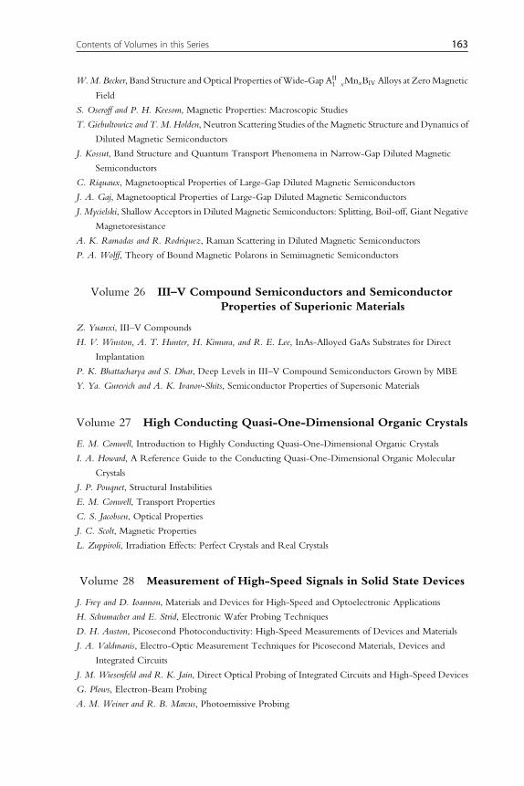
W.M. Becker, Band Structure andOptical Properties ofWide-Gap AII1�xMnxBIV Alloys at ZeroMagnetic
Field
S. Oseroff and P. H. Keesom, Magnetic Properties: Macroscopic Studies
T. Giebultowicz and T. M. Holden, Neutron Scattering Studies of theMagnetic Structure and Dynamics of
Diluted Magnetic Semiconductors
J. Kossut, Band Structure and Quantum Transport Phenomena in Narrow-Gap Diluted Magnetic
Semiconductors
C. Riquaux, Magnetooptical Properties of Large-Gap Diluted Magnetic Semiconductors
J. A. Gaj, Magnetooptical Properties of Large-Gap Diluted Magnetic Semiconductors
J. Mycielski, Shallow Acceptors in Diluted Magnetic Semiconductors: Splitting, Boil-off, Giant Negative
Magnetoresistance
A. K. Ramadas and R. Rodriquez, Raman Scattering in Diluted Magnetic Semiconductors
P. A. Wolff, Theory of Bound Magnetic Polarons in Semimagnetic Semiconductors
Volume 26 III–V Compound Semiconductors and Semiconductor
Properties of Superionic Materials
Z. Yuanxi, III–V Compounds
H. V. Winston, A. T. Hunter, H. Kimura, and R. E. Lee, InAs-Alloyed GaAs Substrates for Direct
Implantation
P. K. Bhattacharya and S. Dhar, Deep Levels in III–V Compound Semiconductors Grown by MBE
Y. Ya. Gurevich and A. K. Ivanov-Shits, Semiconductor Properties of Supersonic Materials
Volume 27 High Conducting Quasi-One-Dimensional Organic Crystals
E. M. Conwell, Introduction to Highly Conducting Quasi-One-Dimensional Organic Crystals
I. A. Howard, A Reference Guide to the Conducting Quasi-One-Dimensional Organic Molecular
Crystals
J. P. Pouqnet, Structural Instabilities
E. M. Conwell, Transport Properties
C. S. Jacobsen, Optical Properties
J. C. Scolt, Magnetic Properties
L. Zuppiroli, Irradiation Effects: Perfect Crystals and Real Crystals
Volume 28 Measurement of High-Speed Signals in Solid State Devices
J. Frey and D. Ioannou, Materials and Devices for High-Speed and Optoelectronic Applications
H. Schumacher and E. Strid, Electronic Wafer Probing Techniques
D. H. Auston, Picosecond Photoconductivity: High-Speed Measurements of Devices and Materials
J. A. Valdmanis, Electro-Optic Measurement Techniques for Picosecond Materials, Devices and
Integrated Circuits
J. M. Wiesenfeld and R. K. Jain, Direct Optical Probing of Integrated Circuits and High-Speed Devices
G. Plows, Electron-Beam Probing
A. M. Weiner and R. B. Marcus, Photoemissive Probing
163Contents of Volumes in this Series
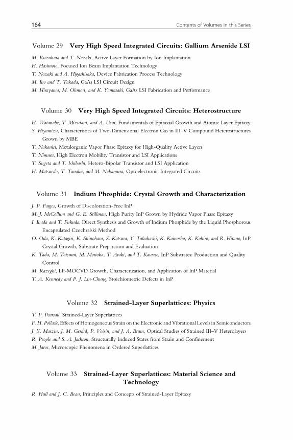
Volume 29 Very High Speed Integrated Circuits: Gallium Arsenide LSI
M. Kuzuhara and T. Nazaki, Active Layer Formation by Ion Implantation
H. Hasimoto, Focused Ion Beam Implantation Technology
T. Nozaki and A. Higashisaka, Device Fabrication Process Technology
M. Ino and T. Takada, GaAs LSI Circuit Design
M. Hirayama, M. Ohmori, and K. Yamasaki, GaAs LSI Fabrication and Performance
Volume 30 Very High Speed Integrated Circuits: Heterostructure
H. Watanabe, T. Mizutani, and A. Usui, Fundamentals of Epitaxial Growth and Atomic Layer Epitaxy
S. Hiyamizu, Characteristics of Two-Dimensional Electron Gas in III–V Compound Heterostructures
Grown by MBE
T. Nakanisi, Metalorganic Vapor Phase Epitaxy for High-Quality Active Layers
T. Nimura, High Electron Mobility Transistor and LSI Applications
T. Sugeta and T. Ishibashi, Hetero-Bipolar Transistor and LSI Application
H. Matsuedo, T. Tanaka, and M. Nakamura, Optoelectronic Integrated Circuits
Volume 31 Indium Phosphide: Crystal Growth and Characterization
J. P. Farges, Growth of Discoloration-Free InP
M. J. McCollum and G. E. Stillman, High Purity InP Grown by Hydride Vapor Phase Epitaxy
I. Inada and T. Fukuda, Direct Synthesis and Growth of Indium Phosphide by the Liquid Phosphorous
Encapsulated Czochralski Method
O. Oda, K. Katagiri, K. Shinohara, S. Katsura, Y. Takahashi, K. Kainosho, K. Kohiro, and R. Hirano, InP
Crystal Growth, Substrate Preparation and Evaluation
K. Tada, M. Tatsumi, M. Morioka, T. Araki, and T. Kawase, InP Substrates: Production and Quality
Control
M. Razeghi, LP-MOCVD Growth, Characterization, and Application of InP Material
T. A. Kennedy and P. J. Lin-Chung, Stoichiometric Defects in InP
Volume 32 Strained-Layer Superlattices: Physics
T. P. Pearsall, Strained-Layer Superlattices
F. H. Pollack, Effects of Homogeneous Strain on the Electronic and Vibrational Levels in Semiconductors
J. Y. Marzin, J. M. Gerard, P. Voisin, and J. A. Brum, Optical Studies of Strained III–V Heterolayers
R. People and S. A. Jackson, Structurally Induced States from Strain and Confinement
M. Jaros, Microscopic Phenomena in Ordered Superlattices
Volume 33 Strained-Layer Superlattices: Material Science and
Technology
R. Hull and J. C. Bean, Principles and Concepts of Strained-Layer Epitaxy
164 Contents of Volumes in this Series
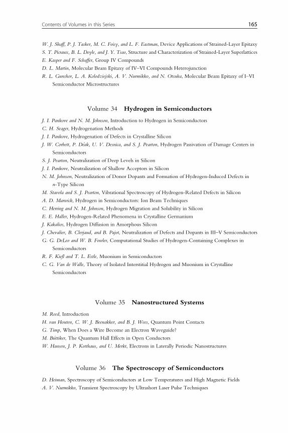
W. J. Shaff, P. J. Tasker, M. C. Foisy, and L. F. Eastman, Device Applications of Strained-Layer Epitaxy
S. T. Picraux, B. L. Doyle, and J. Y. Tsao, Structure and Characterization of Strained-Layer Superlattices
E. Kasper and F. Schaffer, Group IV Compounds
D. L. Martin, Molecular Beam Epitaxy of IV–VI Compounds Heterojunction
R. L. Gunshor, L. A. Kolodziejski, A. V. Nurmikko, and N. Otsuka, Molecular Beam Epitaxy of I–VI
Semiconductor Microstructures
Volume 34 Hydrogen in Semiconductors
J. I. Pankove and N. M. Johnson, Introduction to Hydrogen in Semiconductors
C. H. Seager, Hydrogenation Methods
J. I. Pankove, Hydrogenation of Defects in Crystalline Silicon
J. W. Corbett, P. Deak, U. V. Desnica, and S. J. Pearton, Hydrogen Passivation of Damage Centers in
Semiconductors
S. J. Pearton, Neutralization of Deep Levels in Silicon
J. I. Pankove, Neutralization of Shallow Acceptors in Silicon
N. M. Johnson, Neutralization of Donor Dopants and Formation of Hydrogen-Induced Defects in
n-Type Silicon
M. Stavola and S. J. Pearton, Vibrational Spectroscopy of Hydrogen-Related Defects in Silicon
A. D. Marwick, Hydrogen in Semiconductors: Ion Beam Techniques
C. Herring and N. M. Johnson, Hydrogen Migration and Solubility in Silicon
E. E. Haller, Hydrogen-Related Phenomena in Crystalline Germanium
J. Kakalios, Hydrogen Diffusion in Amorphous Silicon
J. Chevalier, B. Clerjaud, and B. Pajot, Neutralization of Defects and Dopants in III–V Semiconductors
G. G. DeLeo and W. B. Fowler, Computational Studies of Hydrogen-Containing Complexes in
Semiconductors
R. F. Kiefl and T. L. Estle, Muonium in Semiconductors
C. G. Van de Walle, Theory of Isolated Interstitial Hydrogen and Muonium in Crystalline
Semiconductors
Volume 35 Nanostructured Systems
M. Reed, Introduction
H. van Houten, C. W. J. Beenakker, and B. J. Wees, Quantum Point Contacts
G. Timp, When Does a Wire Become an Electron Waveguide?
M. Buttiker, The Quantum Hall Effects in Open Conductors
W. Hansen, J. P. Kotthaus, and U. Merkt, Electrons in Laterally Periodic Nanostructures
Volume 36 The Spectroscopy of Semiconductors
D. Heiman, Spectroscopy of Semiconductors at Low Temperatures and High Magnetic Fields
A. V. Nurmikko, Transient Spectroscopy by Ultrashort Laser Pulse Techniques
165Contents of Volumes in this Series
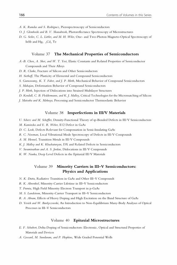
A. K. Ramdas and S. Rodriguez, Piezospectroscopy of Semiconductors
O. J. Glembocki and B. V. Shanabrook, Photoreflectance Spectroscopy of Microstructures
D. G. Seiler, C. L. Littler, and M. H. Wiler, One- and Two-Photon Magneto-Optical Spectroscopy of
InSb and Hg1�xCdx Te
Volume 37 The Mechanical Properties of Semiconductors
A.-B. Chen, A. Sher, and W. T. Yost, Elastic Constants and Related Properties of Semiconductor
Compounds and Their Alloys
D. R. Clarke, Fracture of Silicon and Other Semiconductors
H. Siethoff, The Plasticity of Elemental and Compound Semiconductors
S. Guruswamy, K. T. Faber, and J. P. Hirth, Mechanical Behavior of Compound Semiconductors
S. Mahajan, Deformation Behavior of Compound Semiconductors
J. P. Hirth, Injection of Dislocations into Strained Multilayer Structures
D. Kendall, C. B. Fleddermann, and K. J. Malloy, Critical Technologies for the Micromatching of Silicon
J. Matsuba and K. Mokuya, Processing and Semiconductor Thermoelastic Behavior
Volume 38 Imperfections in III/V Materials
U. Scherz and M. Scheffler, Density-Functional Theory of sp-Bonded Defects in III/V Semiconductors
M. Kaminska and E. R. Weber, E12 Defect in GaAs
D. C. Look, Defects Relevant for Compensation in Semi-Insulating GaAs
R. C. Newman, Local Vibrational Mode Spectroscopy of Defects in III/V Compounds
A. M. Hennel, Transition Metals in III/V Compounds
K. J. Malloy and K. Khachaturyan, DX and Related Defects in Semiconductors
V. Swaminathan and A. S. Jordan, Dislocations in III/V Compounds
K. W. Nauka, Deep Level Defects in the Epitaxial III/V Materials
Volume 39 Minority Carriers in III–V Semiconductors:
Physics and Applications
N. K. Dutta, Radiative Transition in GaAs and Other III–V Compounds
R. K. Ahrenkiel, Minority-Carrier Lifetime in III–V Semiconductors
T. Furuta, High Field Minority Electron Transport in p-GaAs
M. S. Lundstrom, Minority-Carrier Transport in III–V Semiconductors
R. A. Abram, Effects of Heavy Doping and High Excitation on the Band Structure of GaAs
D. Yevick and W. Bardyszewski, An Introduction to Non-Equilibrium Many-Body Analyses of Optical
Processes in III–V Semiconductors
Volume 40 Epitaxial Microstructures
E. F. Schubert, Delta-Doping of Semiconductors: Electronic, Optical and Structural Properties of
Materials and Devices
A. Gossard, M. Sundaram, and P. Hopkins, Wide Graded Potential Wells
166 Contents of Volumes in this Series
P. Petroff, Direct Growth of Nanometer-Size Quantum Wire Superlattices
E. Kapon, Lateral Patterning of Quantum Well Heterostructures by Growth of Nonplanar Substrates
H. Temkin, D. Gershoni, and M. Panish, Optical Properties of Ga1�xInxAs/InP Quantum Wells
Volume 41 High Speed Heterostructure Devices
F. Capasso, F. Beltram, S. Sen, A. Pahlevi, and A. Y. Cho, Quantum Electron Devices: Physics and
Applications
P. Solomon, D. J. Frank, S. L. Wright and F. Canora, GaAs-Gate Semiconductor-Insulator-
Semiconductor FET
M. H. Hashemi and U. K. Mishra, Unipolar InP-Based Transistors
R. Kiehl, Complementary Heterostructure FET Integrated Circuits
T. Ishibashi, GaAs-Based and InP-Based Heterostructure Bipolar-Transistors
H. C. Liu and T. C. L. G. Sollner, High-Frequency-Tunneling Devices
H. Ohnishi, T. More, M. Takatsu, K. Imamura, and N. Yokoyama, Resonant-Tunneling Hot-Electron
Transistors and Circuits
Volume 42 Oxygen in Silicon
F. Shimura, Introduction to Oxygen in Silicon
W. Lin, The Incorporation of Oxygen into Silicon Crystals
T. J. Schaffner and D. K. Schroder, Characterization Techniques for Oxygen in Silicon
W. M. Bullis, Oxygen Concentration Measurement
S. M. Hu, Intrinsic Point Defects in Silicon
B. Pajot, Some Atomic Configuration of Oxygen
J. Michel and L. C. Kimerling, Electrical Properties of Oxygen in Silicon
R. C. Newman and R. Jones, Diffusion of Oxygen in Silicon
T. Y. Tan and W. J. Taylor, Mechanisms of Oxygen Precipitation: Some Quantitative Aspects
M. Schrems, Simulation of Oxygen Precipitation
K. Simino and I. Yonenaga, Oxygen Effect on Mechanical Properties
W. Bergholz, Grown-in and Process-Induced Effects
F. Shimura, Intrinsic/Internal Gettering
H. Tsuya, Oxygen Effect on Electronic Device Performance
Volume 43 Semiconductors for Room Temperature Nuclear
Detector Applications
R. B. James and T. E. Schlesinger, Introduction and Overview
L. S. Darken and C. E. Cox, High-Purity Germanium Detectors
A. Burger, D. Nason, L. Van den Berg, and M. Schieber, Growth of Mercuric Iodide
X. J. Bao, T. E. Schlesinger, and R. B. James, Electrical Properties of Mercuric Iodide
X. J. Bao, R. B. James, and T. E. Schlesinger, Optical Properties of Red Mercuric Iodide
M. Hage-Ali and P. Siffert, Growth Methods of CdTe Nuclear Detector Materials
M. Hage-Ali and P. Siffert, Characterization of CdTe Nuclear Detector Materials
167Contents of Volumes in this Series
M. Hage-Ali and P. Siffert, CdTe Nuclear Detectors and Applications
R. B. James, T. E. Schlesinger, J. Lund, and M. Schieber, Cd1�x Znx Te Spectrometers for Gamma and
X-Ray Applications
D. S. McGregor, J. E. Kammeraad, Gallium Arsenide Radiation Detectors and Spectrometers
J. C. Lund, F. Olschner, and A. Burger, Lead Iodide
M. R. Squillante and K. S. Shah, Other Materials: Status and Prospects
V. M. Gerrish, Characterization and Quantification of Detector Performance
J. S. Iwanczyk and B. E. Patt, Electronics for X-ray and Gamma Ray Spectrometers
M. Schieber, R. B. James and T. E. Schlesinger, Summary and Remaining Issues for Room Temperature
Radiation Spectrometers
Volume 44 II–IV Blue/Green Light Emitters: Device Physics
and Epitaxial Growth
J. Han and R. L. Gunshor, MBE Growth and Electrical Properties of Wide Bandgap ZnSe-based
II–VI Semiconductors
S. Fujita and S. Fujita, Growth and Characterization of ZnSe-based II–VI Semiconductors by MOVPE
E. Ho and L. A. Kolodziejski, Gaseous Source UHV Epitaxy Technologies for Wide Bandgap II–VI
Semiconductors
C. G. Van de Walle, Doping of Wide-Band-Gap II–VI Compounds – Theory
R. Cingolani, Optical Properties of Excitons in ZnSe-Based Quantum Well Heterostructures
A. Ishibashi and A. V. Nurmikko, II–VI Diode Lasers: A Current View of Device Performance and Issues
S. Guha and J. Petruzello, Defects and Degradation in Wide-Gap II–VI-based Structure and Light
Emitting Devices
Volume 45 Effect of Disorder and Defects in Ion-Implanted
Semiconductors: Electrical and Physiochemical Characterization
H. Ryssel, Ion Implantation into Semiconductors: Historical Perspectives
You-Nian Wang and Teng-Cai Ma, Electronic Stopping Power for Energetic Ions in Solids
S. T. Nakagawa, Solid Effect on the Electronic Stopping of Crystalline Target and Application to Range
Estimation
G. Miller, S. Kalbitzer, and G. N. Greaves, Ion Beams in Amorphous Semiconductor Research
J. Boussey-Said, Sheet and Spreading Resistance Analysis of Ion Implanted and Annealed Semiconductors
M. L. Polignano and G. Queirolo, Studies of the Stripping Hall Effect in Ion-Implanted Silicon
J. Sroemenos, Transmission Electron Microscopy Analyses
R. Nipoti and M. Servidori, Rutherford Backscattering Studies of Ion Implanted Semiconductors
P. Zaumseil, X-ray Diffraction Techniques
Volume 46 Effect of Disorder and Defects in Ion-Implanted
Semiconductors: Optical and Photothermal Characterization
M. Fried, T. Lohner, and J. Gyulai, Ellipsometric Analysis
A. Seas and C. Christofides, Transmission and Reflection Spectroscopy on Ion Implanted Semiconductors
168 Contents of Volumes in this Series

A. Othonos and C. Christofides, Photoluminescence and Raman Scattering of Ion Implanted
Semiconductors. Influence of Annealing
C. Christofides, Photomodulated Thermoreflectance Investigation of Implanted Wafers. Annealing
Kinetics of Defects
U. Zammit, Photothermal Deflection Spectroscopy Characterization of Ion-Implanted and Annealed
Silicon Films
A.Mandelis, A. Budiman, and M. Vargas, Photothermal Deep-Level Transient Spectroscopy of Impurities
and Defects in Semiconductors
R. Kalish and S. Charbonneau, Ion Implantation into Quantum-Well Structures
A. M. Myasnikov and N. N. Gerasimenko, Ion Implantation and Thermal Annealing of III–V Compound
Semiconducting Systems: Some Problems of III–V Narrow Gap Semiconductors
Volume 47 Uncooled Infrared Imaging Arrays and Systems
R. G. Buser and M. P. Tompsett, Historical Overview
P. W. Kruse, Principles of Uncooled Infrared Focal Plane Arrays
R. A. Wood, Monolithic Silicon Microbolometer Arrays
C. M. Hanson, Hybrid Pyroelectric-Ferroelectric Bolometer Arrays
D. L. Polla and J. R. Choi, Monolithic Pyroelectric Bolometer Arrays
N. Teranishi, Thermoelectric Uncooled Infrared Focal Plane Arrays
M. F. Tompsett, Pyroelectric Vidicon
T. W. Kenny, Tunneling Infrared Sensors
J. R. Vig, R. L Filler, and Y. Kim, Application of Quartz Microresonators to Uncooled Infrared Imaging
Arrays
P. W. Kruse, Application of Uncooled Monolithic Thermoelectric Linear Arrays to Imaging
Radiometers
Volume 48 High Brightness Light Emitting Diodes
G. B. Stringfellow, Materials Issues in High-Brightness Light-Emitting Diodes
M. G. Craford, Overview of Device Issues in High-Brightness Light-Emitting Diodes
F. M. Steranka, AlGaAs Red Light Emitting Diodes
C. H. Chen, S. A. Stockman, M. J. Peanasky, and C. P. Kuo, OMVPE Growth of AlGaInP for High
Efficiency Visible Light-Emitting Diodes
F. A. Kish and R. M. Fletcher, AlGaInP Light-Emitting Diodes
M. W. Hodapp, Applications for High Brightness Light-Emitting Diodes
J. Akasaki and H. Amano, Organometallic Vapor Epitaxy of GaN for High Brightness Blue Light Emitting
Diodes
S. Nakamura, Group III–V Nitride Based Ultraviolet-Blue-Green-Yellow Light-Emitting Diodes and
Laser Diodes
Volume 49 Light Emission in Silicon: from Physics to Devices
D. J. Lockwood, Light Emission in Silicon
G. Abstreiter, Band Gaps and Light Emission in Si/SiGe Atomic Layer Structures
169Contents of Volumes in this Series
T. G. Brown and D. G. Hall, Radiative Isoelectronic Impurities in Silicon and Silicon-GermaniumAlloys
and Superlattices
J. Michel, L. V. C. Assali, M. T. Morse, and L. C. Kimerling, Erbium in Silicon
Y. Kanemitsu, Silicon and Germanium Nanoparticles
P. M. Fauchet, Porous Silicon: Photoluminescence and Electroluminescent Devices
C. Delerue, G. Allan, and M. Lannoo, Theory of Radiative and Nonradiative Processes in Silicon
Nanocrystallites
L. Brus, Silicon Polymers and Nanocrystals
Volume 50 Gallium Nitride (GaN)
J. I. Pankove and T. D. Moustakas, Introduction
S. P. DenBaars and S. Keller, Metalorganic Chemical Vapor Deposition (MOCVD) of Group III Nitrides
W. A. Bryden and T. J. Kistenmacher, Growth of Group III–A Nitrides by Reactive Sputtering
N. Newman, Thermochemistry of III–N Semiconductors
S. J. Pearton and R. J. Shul, Etching of III Nitrides
S. M. Bedair, Indium-based Nitride Compounds
A. Trampert, O. Brandt, and K. H. Ploog, Crystal Structure of Group III Nitrides
H. Morkoc, F. Hamdani, and A. Salvador, Electronic and Optical Properties of III–V Nitride based
Quantum Wells and Superlattices
K. Doverspike and J. I. Pankove, Doping in the III-Nitrides
T. Suski and P. Perlin, High Pressure Studies of Defects and Impurities in Gallium Nitride
B. Monemar, Optical Properties of GaN
W. R. L. Lambrecht, Band Structure of the Group III Nitrides
N. E. Christensen and P. Perlin, Phonons and Phase Transitions in GaN
S. Nakamura, Applications of LEDs and LDs
I. Akasaki and H. Amano, Lasers
J. A. Cooper, Jr., Nonvolatile Random Access Memories in Wide Bandgap Semiconductors
Volume 51A Identification of Defects in Semiconductors
G. D. Watkins, EPR and ENDOR Studies of Defects in Semiconductors
J.-M. Spaeth, Magneto-Optical and Electrical Detection of Paramagnetic Resonance in Semiconductors
T. A. Kennedy and E. R. Claser, Magnetic Resonance of Epitaxial Layers Detected by Photoluminescence
K.H. Chow, B. Hitti, and R. F. Kiefl, μSRonMuonium in Semiconductors and Its Relation toHydrogen
K. Saarinen, P. Hautojarvi, and C. Corbel, Positron Annihilation Spectroscopy of Defects in
Semiconductors
R. Jones and P. R. Briddon, TheAb InitioCluster Method and the Dynamics of Defects in Semiconductors
Volume 51B Identification Defects in Semiconductors
G. Davies, Optical Measurements of Point Defects
P. M. Mooney, Defect Identification Using Capacitance Spectroscopy
170 Contents of Volumes in this Series
M. Stavola, Vibrational Spectroscopy of Light Element Impurities in Semiconductors
P. Schwander, W. D. Rau, C. Kisielowski, M. Gribelyuk, and A. Ourmazd, Defect Processes in
Semiconductors Studied at the Atomic Level by Transmission Electron Microscopy
N. D. Jager and E. R. Weber, Scanning Tunneling Microscopy of Defects in Semiconductors
Volume 52 SiC Materials and Devices
K. Jarrendahl and R. F. Davis, Materials Properties and Characterization of SiC
V. A. Dmitiriev and M. G. Spencer, SiC Fabrication Technology: Growth and Doping
V. Saxena and A. J. Steckl, Building Blocks for SiCDevices: Ohmic Contacts, Schottky Contacts, and p-n
Junctions
M. S. Shur, SiC Transistors
C. D. Brandt, R. C. Clarke, R. R. Siergiej, J. B. Casady, A.W.Morse, S. Sriram, and A. K. Agarwal, SiC for
Applications in High-Power Electronics
R. J. Trew, SiC Microwave Devices
J. Edmond, H. Kong, G. Negley, M. Leonard, K. Doverspike, W. Weeks, A. Suvorov, D. Waltz, and
C. Carter, Jr., SiC-Based UV Photodiodes and Light-Emitting Diodes
H. Morkoc, Beyond Silicon Carbide! III–V Nitride-Based Heterostructures and Devices
Volume 53 Cumulative Subjects and Author Index Including Tables
of Contents for Volumes 1–50
Volume 54 High Pressure in Semiconductor Physics I
W. Paul, High Pressure in Semiconductor Physics: A Historical Overview
N. E. Christensen, Electronic Structure Calculations for Semiconductors Under Pressure
R. J. Neimes andM. I. McMahon, Structural Transitions in the Group IV, III–V and II–VI Semiconductors
Under Pressure
A. R. Goni and K. Syassen, Optical Properties of Semiconductors Under Pressure
P. Trautman, M. Baj, and J. M. Baranowski, Hydrostatic Pressure and Uniaxial Stress in Investigations of
the EL2 Defect in GaAs
M. Li and P. Y. Yu, High-Pressure Study of DX Centers Using Capacitance Techniques
T. Suski, Spatial Correlations of Impurity Charges in Doped Semiconductors
N. Kuroda, Pressure Effects on the Electronic Properties of Diluted Magnetic Semiconductors
Volume 55 High Pressure in Semiconductor Physics II
D. K. Maude and J. C. Portal, Parallel Transport in Low-Dimensional Semiconductor Structures
P. C. Klipstein, Tunneling Under Pressure: High-Pressure Studies of Vertical Transport in
Semiconductor Heterostructures
E. Anastassakis and M. Cardona, Phonons, Strains, and Pressure in Semiconductors
171Contents of Volumes in this Series
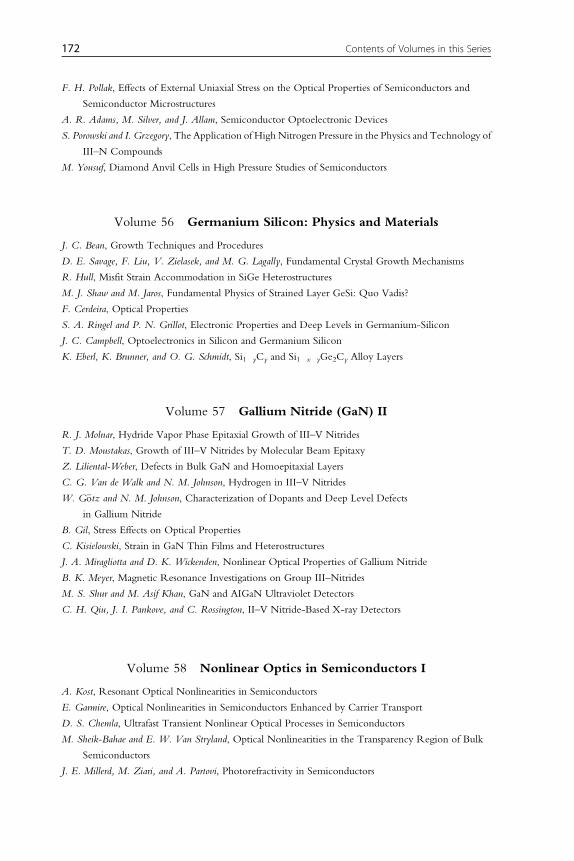
F. H. Pollak, Effects of External Uniaxial Stress on the Optical Properties of Semiconductors and
Semiconductor Microstructures
A. R. Adams, M. Silver, and J. Allam, Semiconductor Optoelectronic Devices
S. Porowski and I. Grzegory, The Application of High Nitrogen Pressure in the Physics and Technology of
III–N Compounds
M. Yousuf, Diamond Anvil Cells in High Pressure Studies of Semiconductors
Volume 56 Germanium Silicon: Physics and Materials
J. C. Bean, Growth Techniques and Procedures
D. E. Savage, F. Liu, V. Zielasek, and M. G. Lagally, Fundamental Crystal Growth Mechanisms
R. Hull, Misfit Strain Accommodation in SiGe Heterostructures
M. J. Shaw and M. Jaros, Fundamental Physics of Strained Layer GeSi: Quo Vadis?
F. Cerdeira, Optical Properties
S. A. Ringel and P. N. Grillot, Electronic Properties and Deep Levels in Germanium-Silicon
J. C. Campbell, Optoelectronics in Silicon and Germanium Silicon
K. Eberl, K. Brunner, and O. G. Schmidt, Si1�yCy and Si1�x�yGe2Cy Alloy Layers
Volume 57 Gallium Nitride (GaN) II
R. J. Molnar, Hydride Vapor Phase Epitaxial Growth of III–V Nitrides
T. D. Moustakas, Growth of III–V Nitrides by Molecular Beam Epitaxy
Z. Liliental-Weber, Defects in Bulk GaN and Homoepitaxial Layers
C. G. Van de Walk and N. M. Johnson, Hydrogen in III–V Nitrides
W. G€otz and N. M. Johnson, Characterization of Dopants and Deep Level Defects
in Gallium Nitride
B. Gil, Stress Effects on Optical Properties
C. Kisielowski, Strain in GaN Thin Films and Heterostructures
J. A. Miragliotta and D. K. Wickenden, Nonlinear Optical Properties of Gallium Nitride
B. K. Meyer, Magnetic Resonance Investigations on Group III–Nitrides
M. S. Shur and M. Asif Khan, GaN and AIGaN Ultraviolet Detectors
C. H. Qiu, J. I. Pankove, and C. Rossington, II–V Nitride-Based X-ray Detectors
Volume 58 Nonlinear Optics in Semiconductors I
A. Kost, Resonant Optical Nonlinearities in Semiconductors
E. Garmire, Optical Nonlinearities in Semiconductors Enhanced by Carrier Transport
D. S. Chemla, Ultrafast Transient Nonlinear Optical Processes in Semiconductors
M. Sheik-Bahae and E. W. Van Stryland, Optical Nonlinearities in the Transparency Region of Bulk
Semiconductors
J. E. Millerd, M. Ziari, and A. Partovi, Photorefractivity in Semiconductors
172 Contents of Volumes in this Series
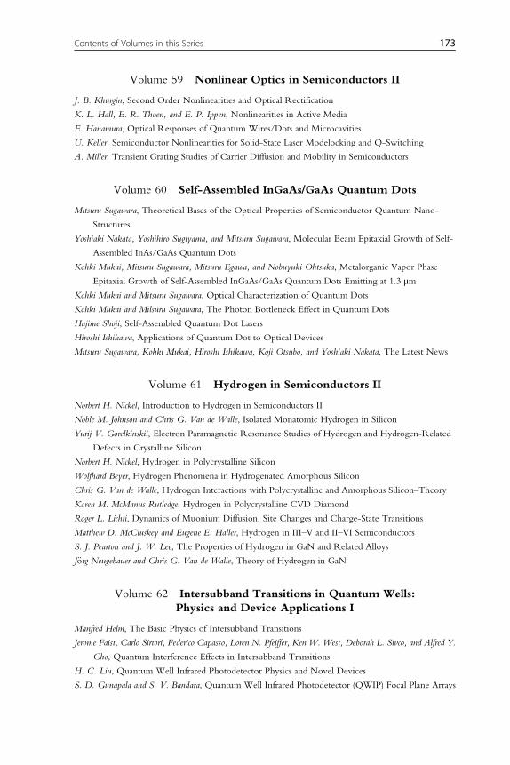
Volume 59 Nonlinear Optics in Semiconductors II
J. B. Khurgin, Second Order Nonlinearities and Optical Rectification
K. L. Hall, E. R. Thoen, and E. P. Ippen, Nonlinearities in Active Media
E. Hanamura, Optical Responses of Quantum Wires/Dots and Microcavities
U. Keller, Semiconductor Nonlinearities for Solid-State Laser Modelocking and Q-Switching
A. Miller, Transient Grating Studies of Carrier Diffusion and Mobility in Semiconductors
Volume 60 Self-Assembled InGaAs/GaAs Quantum Dots
Mitsuru Sugawara, Theoretical Bases of the Optical Properties of Semiconductor Quantum Nano-
Structures
Yoshiaki Nakata, Yoshihiro Sugiyama, and Mitsuru Sugawara, Molecular Beam Epitaxial Growth of Self-
Assembled InAs/GaAs Quantum Dots
Kohki Mukai, Mitsuru Sugawara, Mitsuru Egawa, and Nobuyuki Ohtsuka, Metalorganic Vapor Phase
Epitaxial Growth of Self-Assembled InGaAs/GaAs Quantum Dots Emitting at 1.3 μmKohki Mukai and Mitsuru Sugawara, Optical Characterization of Quantum Dots
Kohki Mukai and Milsuru Sugawara, The Photon Bottleneck Effect in Quantum Dots
Hajime Shoji, Self-Assembled Quantum Dot Lasers
Hiroshi Ishikawa, Applications of Quantum Dot to Optical Devices
Mitsuru Sugawara, Kohki Mukai, Hiroshi Ishikawa, Koji Otsubo, and Yoshiaki Nakata, The Latest News
Volume 61 Hydrogen in Semiconductors II
Norbert H. Nickel, Introduction to Hydrogen in Semiconductors II
Noble M. Johnson and Chris G. Van de Walle, Isolated Monatomic Hydrogen in Silicon
Yurij V. Gorelkinskii, Electron Paramagnetic Resonance Studies of Hydrogen and Hydrogen-Related
Defects in Crystalline Silicon
Norbert H. Nickel, Hydrogen in Polycrystalline Silicon
Wolfhard Beyer, Hydrogen Phenomena in Hydrogenated Amorphous Silicon
Chris G. Van de Walle, Hydrogen Interactions with Polycrystalline and Amorphous Silicon–Theory
Karen M. McManus Rutledge, Hydrogen in Polycrystalline CVD Diamond
Roger L. Lichti, Dynamics of Muonium Diffusion, Site Changes and Charge-State Transitions
Matthew D. McCluskey and Eugene E. Haller, Hydrogen in III–V and II–VI Semiconductors
S. J. Pearton and J. W. Lee, The Properties of Hydrogen in GaN and Related Alloys
J€org Neugebauer and Chris G. Van de Walle, Theory of Hydrogen in GaN
Volume 62 Intersubband Transitions in Quantum Wells:
Physics and Device Applications I
Manfred Helm, The Basic Physics of Intersubband Transitions
Jerome Faist, Carlo Sirtori, Federico Capasso, Loren N. Pfeiffer, Ken W. West, Deborah L. Sivco, and Alfred Y.
Cho, Quantum Interference Effects in Intersubband Transitions
H. C. Liu, Quantum Well Infrared Photodetector Physics and Novel Devices
S. D. Gunapala and S. V. Bandara, Quantum Well Infrared Photodetector (QWIP) Focal Plane Arrays
173Contents of Volumes in this Series
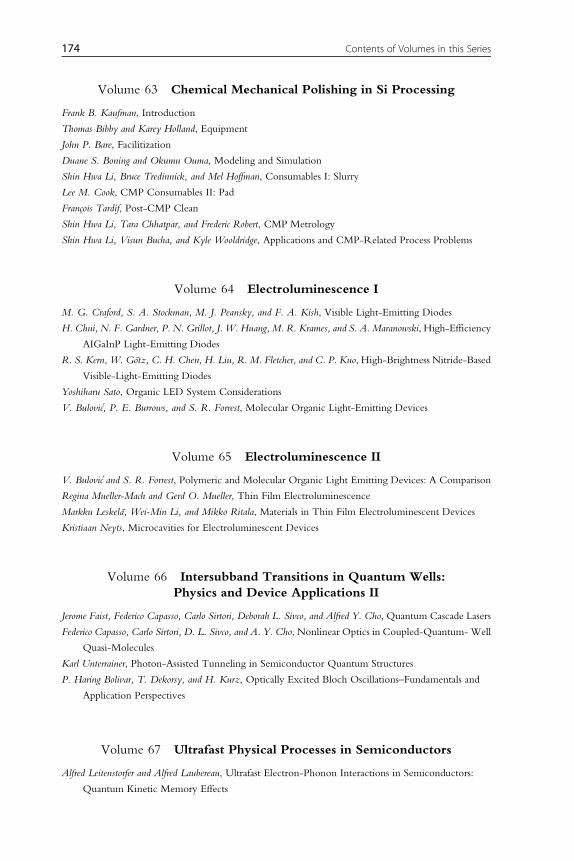
Volume 63 Chemical Mechanical Polishing in Si Processing
Frank B. Kaufman, Introduction
Thomas Bibby and Karey Holland, Equipment
John P. Bare, Facilitization
Duane S. Boning and Okumu Ouma, Modeling and Simulation
Shin Hwa Li, Bruce Tredinnick, and Mel Hoffman, Consumables I: Slurry
Lee M. Cook, CMP Consumables II: Pad
Francois Tardif, Post-CMP Clean
Shin Hwa Li, Tara Chhatpar, and Frederic Robert, CMP Metrology
Shin Hwa Li, Visun Bucha, and Kyle Wooldridge, Applications and CMP-Related Process Problems
Volume 64 Electroluminescence I
M. G. Craford, S. A. Stockman, M. J. Peansky, and F. A. Kish, Visible Light-Emitting Diodes
H. Chui, N. F. Gardner, P. N. Grillot, J. W. Huang, M. R. Krames, and S. A. Maranowski, High-Efficiency
AIGaInP Light-Emitting Diodes
R. S. Kern, W. Gotz, C. H. Chen, H. Liu, R. M. Fletcher, and C. P. Kuo, High-Brightness Nitride-Based
Visible-Light-Emitting Diodes
Yoshiharu Sato, Organic LED System Considerations
V. Bulovic, P. E. Burrows, and S. R. Forrest, Molecular Organic Light-Emitting Devices
Volume 65 Electroluminescence II
V. Bulovic and S. R. Forrest, Polymeric and Molecular Organic Light Emitting Devices: A Comparison
Regina Mueller-Mach and Gerd O. Mueller, Thin Film Electroluminescence
Markku Leskela, Wei-Min Li, and Mikko Ritala, Materials in Thin Film Electroluminescent Devices
Kristiaan Neyts, Microcavities for Electroluminescent Devices
Volume 66 Intersubband Transitions in Quantum Wells:
Physics and Device Applications II
Jerome Faist, Federico Capasso, Carlo Sirtori, Deborah L. Sivco, and Alfred Y. Cho, Quantum Cascade Lasers
Federico Capasso, Carlo Sirtori, D. L. Sivco, and A. Y. Cho, Nonlinear Optics in Coupled-Quantum-Well
Quasi-Molecules
Karl Unterrainer, Photon-Assisted Tunneling in Semiconductor Quantum Structures
P. Haring Bolivar, T. Dekorsy, and H. Kurz, Optically Excited Bloch Oscillations–Fundamentals and
Application Perspectives
Volume 67 Ultrafast Physical Processes in Semiconductors
Alfred Leitenstorfer and Alfred Laubereau, Ultrafast Electron-Phonon Interactions in Semiconductors:
Quantum Kinetic Memory Effects
174 Contents of Volumes in this Series
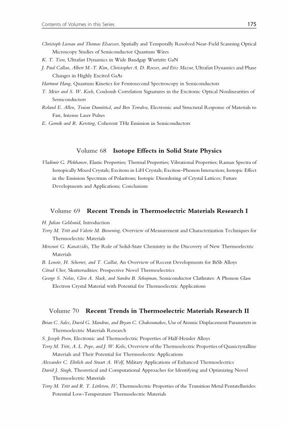
Christoph Lienau and Thomas Elsaesser, Spatially and Temporally Resolved Near-Field Scanning Optical
Microscopy Studies of Semiconductor Quantum Wires
K. T. Tsen, Ultrafast Dynamics in Wide Bandgap Wurtzite GaN
J. Paul Callan, Albert M.-T. Kim, Christopher A. D. Roeser, and Eriz Mazur, Ultrafast Dynamics and Phase
Changes in Highly Excited GaAs
Hartmut Hang, Quantum Kinetics for Femtosecond Spectroscopy in Semiconductors
T. Meier and S. W. Koch, Coulomb Correlation Signatures in the Excitonic Optical Nonlinearities of
Semiconductors
Roland E. Allen, Traian Dumitrica, and Ben Torralva, Electronic and Structural Response of Materials to
Fast, Intense Laser Pulses
E. Gornik and R. Kersting, Coherent THz Emission in Semiconductors
Volume 68 Isotope Effects in Solid State Physics
Vladimir G. Plekhanov, Elastic Properties; Thermal Properties; Vibrational Properties; Raman Spectra of
Isotopically Mixed Crystals; Excitons in LiH Crystals; Exciton–Phonon Interaction; Isotopic Effect
in the Emission Spectrum of Polaritons; Isotopic Disordering of Crystal Lattices; Future
Developments and Applications; Conclusions
Volume 69 Recent Trends in Thermoelectric Materials Research I
H. Julian Goldsmid, Introduction
Terry M. Tritt and Valerie M. Browning, Overview of Measurement and Characterization Techniques for
Thermoelectric Materials
Mercouri G. Kanatzidis, The Role of Solid-State Chemistry in the Discovery of New Thermoelectric
Materials
B. Lenoir, H. Scherrer, and T. Caillat, An Overview of Recent Developments for BiSb Alloys
Citrad Uher, Skutterudities: Prospective Novel Thermoelectrics
George S. Nolas, Glen A. Slack, and Sandra B. Schujman, Semiconductor Clathrates: A Phonon Glass
Electron Crystal Material with Potential for Thermoelectric Applications
Volume 70 Recent Trends in Thermoelectric Materials Research II
Brian C. Sales, David G. Mandrus, and Bryan C. Chakoumakos, Use of Atomic Displacement Parameters in
Thermoelectric Materials Research
S. Joseph Poon, Electronic and Thermoelectric Properties of Half-Heusler Alloys
Terry M. Tritt, A. L. Pope, and J. W. Kolis, Overview of the Thermoelectric Properties of Quasicrystalline
Materials and Their Potential for Thermoelectric Applications
Alexander C. Ehrlich and Stuart A. Wolf, Military Applications of Enhanced Thermoelectrics
David J. Singh, Theoretical and Computational Approaches for Identifying and Optimizing Novel
Thermoelectric Materials
Terry M. Tritt and R. T. Littleton, IV, Thermoelectric Properties of the Transition Metal Pentatellurides:
Potential Low-Temperature Thermoelectric Materials
175Contents of Volumes in this Series
Franz Freibert, Timothy W. Darling, Albert Miglori, and Stuart A. Trugman, Thermomagnetic Effects and
Measurements
M. Bartkowiak and G. D. Mahan, Heat and Electricity Transport Through Interfaces
Volume 71 Recent Trends in Thermoelectric Materials Research III
M. S. Dresselhaus, Y.-M. Lin, T. Koga, S. B. Cronin, O. Rabin, M. R. Black, and G. Dresselhaus, Quantum
Wells and Quantum Wires for Potential Thermoelectric Applications
D. A. Broido and T. L. Reinecke, Thermoelectric Transport in Quantum Well and Quantum Wire
Superlattices
G. D. Mahan, Thermionic Refrigeration
Rama Venkatasubramanian, Phonon Blocking Electron Transmitting Superlattice Structures as Advanced
Thin Film Thermoelectric Materials
G. Chen, Phonon Transport in Low-Dimensional Structures
Volume 72 Silicon Epitaxy
S. Acerboni, ST Microelectronics, CFM-AGI Department, Agrate Brianza, Italy
V.-M. Airaksinen, Okmetic Oyj R&D Department, Vantaa, Finland
G. Beretta, ST Microelectronics, DSG Epitaxy Catania Department, Catania, Italy
C. Cavallotti, Dipartimento di Chimica Fisica Applicata, Politecnico di Milano, Milano, Italy
D. Crippa, MEMC Electronic Materials, Epitaxial and CVD Department, Operations Technology
Division, Novara, Italy
D. Dutartre, ST Microelectronics, Central R&D, Crolles, France
Srikanth Kommu, MEMC Electronic Materials inc., EPI Technology Group, St. Peters, Missouri
M. Masi, Dipartimento di Chimica Fisica Applicata, Politecnico di Milano, Milano, Italy
D. J. Meyer, ASM Epitaxy, Phoenix, Arizona
J. Murota, Research Institute of Electrical Communication, Laboratory for Electronic Intelligent Systems,
Tohoku University, Sendai, Japan
V. Pozzetti, LPE Epitaxial Technologies, Bollate, Italy
A. M. Rinaldi, MEMC Electronic Materials, Epitaxial and CVD Department, Operations Technology
Division, Novara, Italy
Y. Shiraki, Research Center for Advanced Science and Technology (RCAST), University of Tokyo,
Tokyo, Japan
Volume 73 Processing and Properties of Compound Semiconductors
S. J. Pearton, Introduction
Eric Donkor, Gallium Arsenide Heterostructures
Annamraju Kasi Viswanatli, Growth and Optical Properties of GaN
D. Y. C. Lie and K. L. Wang, SiGe/Si Processing
S. Kim and M. Razeghi, Advances in Quantum Dot Structures
Walter P. Gomes, Wet Etching of III–V Semiconductors
176 Contents of Volumes in this Series
Volume 74 Silicon-Germanium Strained Layers and Heterostructures
S. C. Jain and M.Willander, Introduction; Strain, Stability, Reliability and Growth; Mechanism of Strain
Relaxation; Strain, Growth, and TED in SiGeC Layers; Bandstructure and Related Properties;
Heterostructure Bipolar Transistors; FETs and Other Devices
Volume 75 Laser Crystallization of Silicon
Norbert H. Nickel, Introduction to Laser Crystallization of Silicon
Costas P. Grigoropoidos, Seung-Jae Moon and Ming-Hong Lee, Heat Transfer and Phase Transformations in
Laser Melting and Recrystallization of Amorphous Thin Si Films
Robert Cerny and Petr Prikryl, Modeling Laser-Induced Phase-Change Processes: Theory and
Computation
Paulo V. Santos, Laser Interference Crystallization of Amorphous Films
Philipp Lengsfeld and Norbert H. Nickel, Structural and Electronic Properties of Laser-Crystallized Poly-Si
Volume 76 Thin-Film Diamond I
X. Jiang, Textured and Heteroepitaxial CVD Diamond Films
Eberhard Blank, Structural Imperfections in CVD Diamond Films
R. Kalish, Doping Diamond by Ion-Implantation
A. Deneuville, Boron Doping of Diamond Films from the Gas Phase
S. Koizumi, n-Type Diamond Growth
C. E. Nebel, Transport and Defect Properties of Intrinsic and Boron-Doped Diamond
Milos Nesladek, Ken Haenen and Milan Vanecek, Optical Properties of CVD Diamond
Rolf Sauer, Luminescence from Optical Defects and Impurities in CVD Diamond
Volume 77 Thin-Film Diamond II
Jacques Chevallier, Hydrogen Diffusion and Acceptor Passivation in Diamond
J€urgen Ristein, Structural and Electronic Properties of Diamond Surfaces
John C. Angus, Yuri V. Pleskov and Sally C. Eaton, Electrochemistry of Diamond
Greg M. Swain, Electroanalytical Applications of Diamond Electrodes
Werner Haenni, Philippe Rychen, Matthyas Fryda and Christos Comninellis, Industrial Applications of
Diamond Electrodes
Philippe Bergonzo and Richard B. Jackman, Diamond-Based Radiation and Photon Detectors
Hiroshi Kawarada, Diamond Field Effect Transistors Using H-Terminated Surfaces
Shinichi Shikata and Hideaki Nakahata, Diamond Surface Acoustic Wave Device
Volume 78 Semiconducting Chalcogenide Glass I
V. S. Minaev and S. P. Timoshenkov, Glass-Formation in Chalcogenide Systems and Periodic System
A. Popov, Atomic Structure and Structural Modification of Glass
177Contents of Volumes in this Series
V. A. Funtikov, Eutectoidal Concept of Glass Structure and Its Application in Chalcogenide
Semiconductor Glasses
V. S. Minaev, Concept of Polymeric Polymorphous-Crystalloid Structure of Glass and Chalcogenide
Systems: Structure and Relaxation of Liquid and Glass
Volume 79 Semiconducting Chalcogenide Glass II
M. D. Bal’makov, Information Capacity of Condensed Systems
A. Cesnys, G. Juska and E. Montrimas, Charge Carrier Transfer at High Electric Fields in Noncrystalline
Semiconductors
Andrey S. Glebov, The Nature of the Current Instability in Chalcogenide Vitreous Semiconductors
A. M. Andriesh, M. S. Iovu and S. D. Shutov, Optical and Photoelectrical Properties of Chalcogenide
Glasses
V. Val. Sobolev and V. V. Sobolev, Optical Spectra of Arsenic Chalcogenides in a Wide Energy Range of
Fundamental Absorption
Yu. S. Tver’yanovich, Magnetic Properties of Chalcogenide Glasses
Volume 80 Semiconducting Chalcogenide Glass III
Andrey S. Glebov, Electronic Devices and Systems Based on Current Instability in Chalcogenide
Semiconductors
Dumitru Tsiulyanu, Heterostructures on Chalcogenide Glass and Their Applications
E. Bychkov, Yu. Tveryanovich and Yu. Vlasov, Ion Conductivity and Sensors
Yu. S. Tver’yanovich and A. Tverjanovich, Rare-earth Doped Chalcogenide Glass
M. F. Churbanov and V. G. Plotnichenko, Optical Fibers from High-purity Arsenic Chalcogenide Glasses
Volume 81 Conducting Organic Materials and Devices
Suresh C. Jain,Magnus Willander and Vikram Kumar, Introduction; Polyacetylene; Optical and Transport
Properties; Light Emitting Diodes and Lasers; Solar Cells; Transistors
Volume 82 Semiconductors and Semimetals
MaikenH.Mikkelsen, Roberto C.Myers, Gregory D. Fuchs, and David D. Awschalom, Single Spin Coherence
in Semiconductors
Jairo Sinova and A. H. MacDonald, Theory of Spin–Orbit Effects in Semiconductors
K. M. Yu, T. Wojtowicz, W. Walukiewicz, X. Liu, and J. K. Furdyna, Fermi Level Effects on Mn
Incorporation in III–Mn–V Ferromagnetic Semiconductors
T. Jungwirth, B. L. Gallagher, and J.Wunderlich, Transport Properties of Ferromagnetic Semiconductors
F. Matsukura, D. Chiba, and H. Ohno, Spintronic Properties of Ferromagnetic Semiconductors
C. Gould, G. Schmidt, and L. W. Molenkamp, Spintronic Nanodevices
178 Contents of Volumes in this Series
J. Cibert, L. Besombes, D. Ferrand, and H. Mariette, Quantum Structures of II–VI Diluted Magnetic
Semiconductors
Agnieszka Wolos and Maria Kaminska, Magnetic Impurities in Wide Band-gap III–V Semiconductors
Tomasz Dietl, Exchange Interactions and Nanoscale Phase Separations in Magnetically Doped
Semiconductors
Hiroshi Katayama-Yoshida, Kazunori Sato, Tetsuya Fukushima, Masayuki Toyoda, Hidetoshi Kizaki, and An
van Dinh, Computational Nano-Materials Design for the Wide Band-Gap and High-TC
Semiconductor Spintronics
Masaaki Tanaka, Masafumi Yokoyama, PhamNamHai, and Shinobu Ohya, Properties and Functionalities of
MnAs/III–V Hybrid and Composite Structures
Volume 83 Semiconductors and Semimetals
T. Scholak, F. Mintert, T. Wellens, and A. Buchleitner, Transport and Entanglement
P. Nalbach andM. Thorwart, QuantumCoherence and Entanglement in Photosynthetic Light-Harvesting
Complexes
Richard J. Cogdell and J€urgen K€ohler, Sunlight, Purple Bacteria, and Quantum Mechanics: How Purple
Bacteria Harness Quantum Mechanics for Efficient Light Harvesting
Volume 84 Semiconductors and Semimetals
David Z.-Y. Ting, Alexander Soibel, Linda H€oglund, Jean Nguyen, Cory J. Hill, Arezou Khoshakhlagh, and
Sarath D. Gunapala, Type-II Superlattice Infrared Detectors
S. D. Gunapala, S. V. Bandara, S. B. Rafol, and D. Z. Ting, QuantumWell Infrared Photodetectors
Ajit V. Barve and Sanjay Krishna, Quantum Dot Infrared Photodetectors
J. C. Cao and H. C. Liu, Terahertz Semiconductor Quantum Well Photodetectors
A. G. U. Perera, Homo- and Heterojunction InterfacialWorkfunction Internal Photo-Emission
Detectors from UV to IR
David R. Rhiger, HgCdTe Long-Wave Infrared Detectors
Volume 85 Semiconductors and Semimetals
Darius Abramavicius, Vytautas Butkus, and Leonas Valkunas, Interplay of Exciton Coherence and
Dissipation in Molecular Aggregates
Oliver K€uhn and Stefan Lochbrunner, Quantum Dynamics and Spectroscopy of Excitons in Molecular
Aggregates
Carsten Olbrich and Ulrich Kleinekath€ofer, From Atomistic Modeling to Electronic Properties of Light-
Harvesting Systems
AlexW. Chin, Susana F. Huelga, and Martin B. Plenio, Chain Representations of Open Quantum Systems
and Their Numerical Simulation with Time-Adaptive Density Matrix Renormalisation Group
Methods
Avinash Kolli and Alexandra Olaya-Castro, Electronic Excitation Dynamics in a Framework of Shifted
Oscillators
179Contents of Volumes in this Series
E. Lifshitz, R. Vaxenburg, G. I. Maikov, D. Yanover, A. Brusilovski, J. Tilchin, and A. Sashchiuk,
The Significance of Alloy Colloidal Quantum Dots
Elizabeth von Hauff, The Role of Molecular Structure and Conformation in Polymer Electronics
Koen Vandewal, Kristofer Tvingstedt, and Olle Inganas, Charge Transfer States in Organic Donor–Acceptor
Solar Cells
Carsten Deibel, Photocurrent Generation in Organic Solar Cells
Volume 86 Advances in Semiconductor Lasers
Joseph P. Donnelly, Paul W. Juodawlkis, Robin Huang, Jason J. Plant, Gary M. Smith, Leo J. Missaggia,
William Loh, Shawn M. Redmond, Bien Chann, Michael K. Connors, Reuel B. Swint, and George W.
Turner, High-Power Slab-Coupled Optical Waveguide Lasers and Amplifiers
P. Crump, O. Brox, F. Bugge, J. Fricke, C. Schultz, M. Spreemann, B. Sumpf, H. Wenzel, and G. Erbert,
High-Power, High-Efficiency Monolithic Edge-Emitting GaAs-Based Lasers with
Narrow Spectral Widths
E. A. Avrutin and E. U. Rafailov, Advances in Mode-Locked Semiconductor Lasers
K. M. Kelchner, S. P. DenBaars, and J. S. Speck, GaN Laser Diodes on Nonpolar and Semipolar Planes
Eric Tournie and Alexei N. Baranov, Mid-Infrared Semiconductor Lasers: A Review
Dominic F. Siriani and Kent D. Choquette, Coherent Coupling of Vertical-Cavity Surface-Emitting Laser
Arrays
Anne C. Tropper, Adrian H. Quarterman, and Keith G. Wilcox, Ultrafast Vertical-External-Cavity Surface-
Emitting Semiconductor Lasers
Soon-Hong Kwon, Hong-Gyu Park, and Yong-Hee Lee, Photonic Crystal Lasers
Martin T. Hill, Metallic and Plasmonic Nanolasers
Mark T. Crowley, Nader A. Naderi, Hui Su, Frederic Grillot, and Luke F. Lester, GaAs-Based Quantum Dot
Lasers
Philip Poole, InP-Based Quantum Dot Lasers
C. Z. Ning, Semiconductor Nanowire Lasers
Volume 87 Advances in Photovoltaics: Volume 1
Hans-Josef Fell, Foreword
Eicke R. Weber and Gerhard P. Willeke, Introduction
Gerhard P. Willeke and Armin Rauber, On The History of Terrestrial PV Development: With a Focus
on Germany
Paula Mints, Overview of Photovoltaic Production, Markets, and Perspectives
Gregory F. Nemet and Diana Husmann, PV Learning Curves and Cost Dynamics
Martin A. Green, Photovoltaic Material Resources
Laszlo Fabry and Karl Hesse, Crystalline Silicon Feedstock Preparation and Analysis
Volume 88 Oxide Semiconductors
John L. Lyons, Anderson Janotti, and Chris G. Van de Walle, Theory and Modeling of Oxide
Semiconductors
180 Contents of Volumes in this Series

Filip Tuomisto, Open Volume Defects: Positron Annihilation Spectroscopy
Lasse Vines and Andrej Kuznetsov, Bulk Growth and Impurities
Leonard J. Brillson, Surfaces and Interfaces of Zinc Oxide
Tadatsugu Minami, Transparent Conductive Oxides for Transparent Electrode Applications
Bruno K.Meyer, Angelika Polity, Daniel Reppin, Martin Becker, Philipp Hering, Benedikt Kramm, Peter J. Klar,
Thomas Sander, Christian Reindl, Christian Heiliger, Markus Heinemann, Christian M€uller, and Carsten
Ronning, The Physics of Copper Oxide (Cu2O)
Cheng Song and Feng Pan, Transition Metal-Doped Magnetic Oxides
Katharina Grossmann, Udo Weimar, and Nicolae Barsan, Semiconducting Metal Oxides Based Gas Sensors
John F. Wager and Bao Yeh, Oxide Thin-Film Transistors: Device Physics
Volume 89 Advances in Photovoltaics: Part 2
Otwin Breitenstein, The Physics of Industrial Crystalline Silicon Solar Cells
Matthias Heuer, Metallurgical Grade and Metallurgically Refined Silicon for Photovoltaics
Harry Wirth, Crystalline Silicon PV Module Technology
Ulf Blieske and Gunther Stollwerck, Glass and Other Encapsulation Materials
Karsten Bothe and David Hinken, Quantitative Luminescence Characterization of Crystalline Silicon Solar
Cells
Volume 90 Advances in Photovoltaics: Part 3
Giso Hahn and Sebastian Joos, State-of-the-Art Industrial Crystalline Silicon Solar Cells
Christophe Ballif, Stefaan De Wolf, Antoine Descoeudres, and Zachary C. Holman, Amorphous
Silicon/Crystalline Silicon Heterojunction Solar Cells
Bernhard Dimmler, Overview of Thin-Film Solar Cell Technologies
Volume 91 Defects in Semiconductors
Peter Pichler, Role of Defects in the Dopant Diffusion in Si
Arne Nylandsted Larsen and Abdelmadjid Mesli, Electron and Proton Irradiation of Silicon
Enrico Napolitani and Giuliana Impellizzeri, Ion Implantation Defects and Shallow Junctions in Si and Ge
Nicholas G. Rudawski, Aaron G. Lind, and Thomas P.Martin, Defective Solid-Phase Epitaxial Growth of Si
Mangalampalli S.R.N. Kiran, Bianca Haberl, Jodie E. Bradby, and James S. Williams, Nanoindentation of
Silicon and Germanium
Eddy Simoen, Johan Lauwaert, and Henk Vrielinck, Analytical Techniques for Electrically Active Defect
Detection
Daniela Cavalcoli, Beatrice Fraboni, and Anna Cavallini, Surface and Defect States in Semiconductors
Investigated by Surface Photovoltage
Matthew D. McCluskey, Point Defects in ZnO
Michael A. Reshchikov, Point Defects in GaN
Naoya Iwamoto and Bengt G. Svensson, Point Defects in Silicon Carbide
181Contents of Volumes in this Series