Voltage-Controlled Oscillators in Cable Tunersjrogers/Kevin.pdfVoltage-Controlled Oscillators in...
39
A 4 th Year Project Report for Professor J. Rogers Voltage-Controlled Oscillators in Cable Tuners April 9, 2003 Kevin Cheung
-
Upload
hoangkhanh -
Category
Documents
-
view
222 -
download
0
Transcript of Voltage-Controlled Oscillators in Cable Tunersjrogers/Kevin.pdfVoltage-Controlled Oscillators in...

A 4th Year Project Report for Professor J. Rogers
Voltage-Controlled Oscillators in Cable Tuners
April 9, 2003
Kevin Cheung

Abstract
The desire for wide bandwidth receivers is realized in the integrated cable tuner, a
receiver capable of tuning signals ranging from 50 MHz to 850MHz. This project
implements a 1.85 GHz voltage-controlled oscillator, the component that provides the
reference tone that enables the mixers to upconvert, downconvert, or image reject the
signal as required. Implemented monolithically in 0.18 µm CMOS technology, MOS
varactors were designed to achieve maximum tuning range. On-chip spiral inductors
achieving a Q of 5.22 were also created. Lastly, a 3-stage polyphase filter was
implemented to provide a 90˚ phase shift for the image reject mixers. The VCO can
tunes between 1.84 GHz and 1.88 GHz and exhibits phase noise of -109.9 dBc/Hz at a
100 kHz offset and -136 dBc/Hz at a 1 MHz offset.

Table of Contents
List of Figures ..................................................................................................................... i
List of Tables......................................................................................................................ii
Acknowledgements...........................................................................................................iii
1.0 Introduction ........................................................................................................... 1
2.0 Overview of the Integrated Cable Tuner ............................................................ 2
2.1 General Objectives .............................................................................................. 2
2.2 Top Level Design ................................................................................................ 2
2.3 Why Use 0.18 µm CMOS? ................................................................................. 3
3.0 The Voltage-Controlled Oscillator ...................................................................... 5
3.1 The Two VCO’s .................................................................................................. 5
3.2 Specifications ...................................................................................................... 7
3.3 Oscillator Basics.................................................................................................. 7
3.4 Phase Noise ......................................................................................................... 8
4.0 Oscillator Design Process.................................................................................... 11
4.1 The Negative Gm Oscillator .............................................................................. 11
4.2 LC Resonator..................................................................................................... 12
4.3 Varactors ........................................................................................................... 14
4.4 Inductors............................................................................................................ 19
4.5 Polyphase Filters ............................................................................................... 22
4.6 Design Summary............................................................................................... 25

5.0 Simulations and Results...................................................................................... 26
5.1 Transient Response ........................................................................................... 27
5.2 Phase Noise ....................................................................................................... 28
5.3 Results Summary............................................................................................... 29
6.0 Future Work ........................................................................................................ 30
7.0 References ............................................................................................................ 31

i
List of Figures
Figure 1: Cable Tuner Block Diagram............................................................................... 3
Figure 2: Second VCO and Image Reject Mixers.............................................................. 6
Figure 3: Block Diagram of a Feedback Loop................................................................... 8
Figure 4: Negative Gm Oscillator topology...................................................................... 12
Figure 5: The LC Resonator............................................................................................. 14
Figure 6: Cross-Section of a Varactor.............................................................................. 15
Figure 7: Varactor Test Bench ......................................................................................... 16
Figure 8: Smith Chart of Varactor’s Input Impedance..................................................... 17
Figure 9: Normalized Imaginary Impedance vs. Tuning voltage of Varactors................ 18
Figure 10: Inductor Geometry.......................................................................................... 21
Figure 11: 3-Stage Polyphase Filter ................................................................................. 23
Figure 12: Polyphase Filter Testbench............................................................................. 23
Figure 13: Polyphase Filter Testbench Output................................................................. 24
Figure 14: Complete VCO ............................................................................................... 25
Figure 15: VCO Operating Points.................................................................................... 26
Figure 16: Transient Output Signal for Vtune = 0V........................................................... 27
Figure 17: Phase Noise Response .................................................................................... 28

ii
List of Tables
Table 1: Voltage-Controlled Oscillator Specifications ...................................................... 7
Table 2: Inductor Geometry ............................................................................................. 20
Table 3: Inductor Properties at 1.85 GHz ........................................................................ 21
Table 4: Summary of Results ........................................................................................... 29

iii
Acknowledgements
I would like to extend my gratitude and appreciation to all those who have helped to
guide this project in the right direction.
Most importantly, my supervisor,
Dr. John Rogers
His trusty side-kick,
Steve Knox
My talented and always motivated group members,
Derek Van Gaal
Christina George
Vince Karam
Mark Fairbarn
Bi Pham
And, of course,
Senegal
Denmark
Nepal
…those late nights spent together were special.

Introduction 1
1.0 Introduction Society has always imposed high demands on research and development in the
communication industry. Faster and more reliable means of communication are constant
requirements of businesses and ordinary people alike. With the advent of technology and
the rapid growth of the Internet, the ability to instantaneously share vast quantities of
information across the world has become an everyday reality. Today, the Internet and
other novel technologies touch every aspect of our life: from work and school, to home
and entertainment. As a result, increased bandwidth, lower power consumption, and
further cost-effectiveness have become highly sought commodities.
To meet these demands, wide bandwidth solutions must be further developed.
Integrated cable tuners are one such solution. Cable signals are no longer used to just
carry television signals. Today, high speed Internet, digital television, and voice over IP
(VOIP) can be transmitted over the same coaxial cables running into the home. The
creation of a cost-effective cable tuner capable of receiving a wide spectrum of signals
would enable these luxuries to be available in every home. Through this project, the
voltage controlled oscillators for these cable tuners will be investigated and designed in
0.18 µm CMOS technology.

Overview of the Integrated Cable Tuner 2
2.0 Overview of the Integrated Cable Tuner Integrated cable tuners are receivers designed to receive a wide range of
frequencies. While ordinary receivers may have an operational range of a couple of
megahertz (106 Hz), cable tuners are designed to function over a range of about a
gigahertz (109 Hz). This increased bandwidth means that more information can be
transferred along the same cable. Practically, this will mean faster downloads and the
integration of high speed Internet access, digital television, and voice over IP (VOIP)
services into a single device. Functionality can be further integrated as the power supply
for the device can be provided over the same cable. Designed for home use, integrated
cable tuners would reside in a wall-mounted box just outside of the home.
2.1 General Objectives The cable tuner must be able to receive a wide spectrum of signals ranging from
50 MHz to 850 MHz and effectively select and amplify the desired channel. This signal
must be translated through various intermediate frequencies to baseband with a minimal
introduction of noise. The final cable tuner must be able to work reliably in a variety of
temperature ranges and exhibit linearity over the entire frequency range. In addition, low
power consumption and cost-effectiveness are essential for market viability.
2.2 Top Level Design
The cable tuner has been subdivided into a number of smaller components to
simplify the design. As illustrated by the block diagram in Figure 1, the cable signals
enter the home through a standard coaxial cable. The received signals are first amplified
by a low-noise amplifier (LNA) and then sent through the first mixer where they are

Overview of the Integrated Cable Tuner 3
translated to a single IF frequency of 1.8 GHz. This signal is then sent off chip to a
bandpass filter where image signals and noise are eliminated. The refined signal is
amplified again and then sent through the image reject mixer to down convert the signal
from the IF frequency of 1.85 GHz to a second IF frequency of 45 MHz.
Figure 1: Cable Tuner Block Diagram
As the design of the complete cable tuner is a quite involved process, each group
member was assigned a specific component of the cable tuner. I was responsible for the
design of the voltage-controlled oscillators (VCOs).
2.3 Why Use 0.18 µm CMOS?
This project was completed using 0.18µm CMOS technology since CMOS offers
several advantages over bipolar technology and because the technology was readily
available in the labs. CMOS, first of all, offers the potential for larger scale integration
[9] and higher operating frequencies. This, combined with lower power consumption and
lower voltage requirements, may result in increased economical value [9]. CMOS,

Overview of the Integrated Cable Tuner 4
furthermore, enables the implementation of mixed analog-digital designs resulting in
improved functionality and further integration.

The Voltage-Controlled Oscillator 5
3.0 The Voltage-Controlled Oscillator The voltage-controlled oscillator generates a periodic signal that can be used for
many analog and digital applications, wherever a reference tone is required. For the
cable tuner, the voltage-controlled oscillators produce a stable sinusoid signal that act as a
reference frequency for the mixers. These reference frequencies enable the mixers to
translate the input signal to the desired intermediate frequency [1]. As illustrated in the
block diagram above (Figure 1), there are two such oscillators in the cable tuner. Both
oscillators have the same basic design differing primarily in their individual oscillating
frequencies. In addition, each VCO is part of a phase-locked loop. The phase-locked
loop provides the tuning voltage to control the frequency of oscillation. It also works
through feedback to constantly correct itself in case of variations in temperature or noise.
3.1 The Two VCO’s There are two voltage-controlled oscillators in the cable tuner, and each supplies
a reference frequency for the mixers in the circuit. The first mixer up converts the
incoming RF signal, which can range between 50 MHz and 850 MHz, to the common IF
frequency of 1.85 GHz. The first voltage-controlled oscillator, consequently, has a very
wide tuning range; it must be able to tune between 1.9 GHz and 2.7 GHz.
The second voltage-controlled oscillator has two main purposes. First, it provides
the reference frequency for the image reject mixer to down convert the signal from the
first IF frequency of 1.85 GHz to the second IF frequency of 45 MHz. Second, as
illustrated below in Figure 2, the IF signal is actually split and mixed to the second IF
frequency by two frequencies that differ by a ninety-degree phase shift. The summation

The Voltage-Controlled Oscillator 6
of these resulting signals enables the cancellation of the image signals formed around the
carrier as a result of the mixing. The second voltage-controlled oscillator has a tuning
range of 1.82 GHz to 1.87 GHz and produces multiple sinusoids, each shifted in phase by
ninety degrees. For the purposes of this project, more work was dedicated to the second
voltage-controlled oscillator.
Figure 2: Second VCO and Image Reject Mixers

The Voltage-Controlled Oscillator 7
3.2 Specifications
In addition to the tuning requirements specified above, the voltage-controlled
oscillator must meet the following specifications:
Table 1: Voltage-Controlled Oscillator Specifications
Characteristic Specification
Power Supply 3.3 VDC
Current Drain IBias ≤ 15 mA
Oscillator Gain KVCO ≤ 250 MHz/V
Phase Noise at 100 kHz, PN ≤ -103 dBc/Hz at 1 MHz, PN ≤ -123 dBc/Hz
Tuning Voltage 0.3 V ≤ Vtune ≤ 3.0 V
3.3 Oscillator Basics A basic voltage controlled oscillator is comprised of two main components: a
resonator and a feedback loop. The resonator starts the oscillations when supplied with
an impulse current, usually provided by noise in the system. The oscillations, however,
quickly fade as a result of damping, and, consequently, a feedback loop is required to
sustain the oscillations.
The feedback loop is illustrated by the block diagram in Figure 3 below.

The Voltage-Controlled Oscillator 8
Figure 3: Block Diagram of a Feedback Loop
From this diagram, the gain of the system can be represented by the following equation
[1]:
)()(1)(
)()(
21
1
sHsHsH
sVsV
in
out
−= (1)
When the denominator 1 ― H1(s) H2(s) equals zero, the gain becomes infinity and the
conditions for oscillation are met. To sustain oscillations with constant amplitude, the
gain must be equal to 1 and the phase around the loop must be equivalent to 2π radians
(0°, 360°, etc) [2]. Thus the conditions of oscillation can be summarized as follows [1]:
πnsHsH
sHsH
2)()(
1|)(||)(|
21
21
=∠
= (2)
The general approach is to generate a negative resistance in parallel to the resonator
circuit. This overcomes the resistance of the circuit and sustains the oscillations.
3.4 Phase Noise
Illustrated by “skirts” around the carrier frequency, phase noise is the random
fluctuations in the output frequency of the VCO [6]. In the cases of the two VCOs where
output signal frequency is extremely important, excessive phase noise can result in
incomplete image rejection or up-conversion or down-conversion to an undesired IF

The Voltage-Controlled Oscillator 9
frequency. The main contributor to phase noise is the LC resonator, hence the
importance of a high quality factor Q. Improved inductors and large voltage swing of the
oscillations help to minimize the relative phase noise.
The following is an estimate of the oscillator’s phase noise using Leeson’s
equation [6]. The values used are the results obtained from simulation.
∆=
s
ino
PsN
QH
PhaseNoise2
|)(|2
|| 221
ωω
(3)
where Ps = signal power of carrier
|Nin(s)|2 = input noise (kT)
H1 = 1
First, we find the parallel resistance of the resonator, which ends up being equal to
the parallel resistance of the inductor since the varactor’s resistance is extremely high.
Ω===
=
+
∞=
+=
−
−
03.182)3)(85.1)(2)(22.5(
11
11
,
1
,
1
,,
nHGHzLQ
r
r
rrR
ind
indp
indp
indpcappp
πω
Next, the signal power of the carrier can be calculated as follows,
mW
V
RV
Pp
ks
648.33)03.182)(2(
)5.3(
22
2tan
=Ω
=
=
And the quality factor of the oscillator Qosc can be calculated,
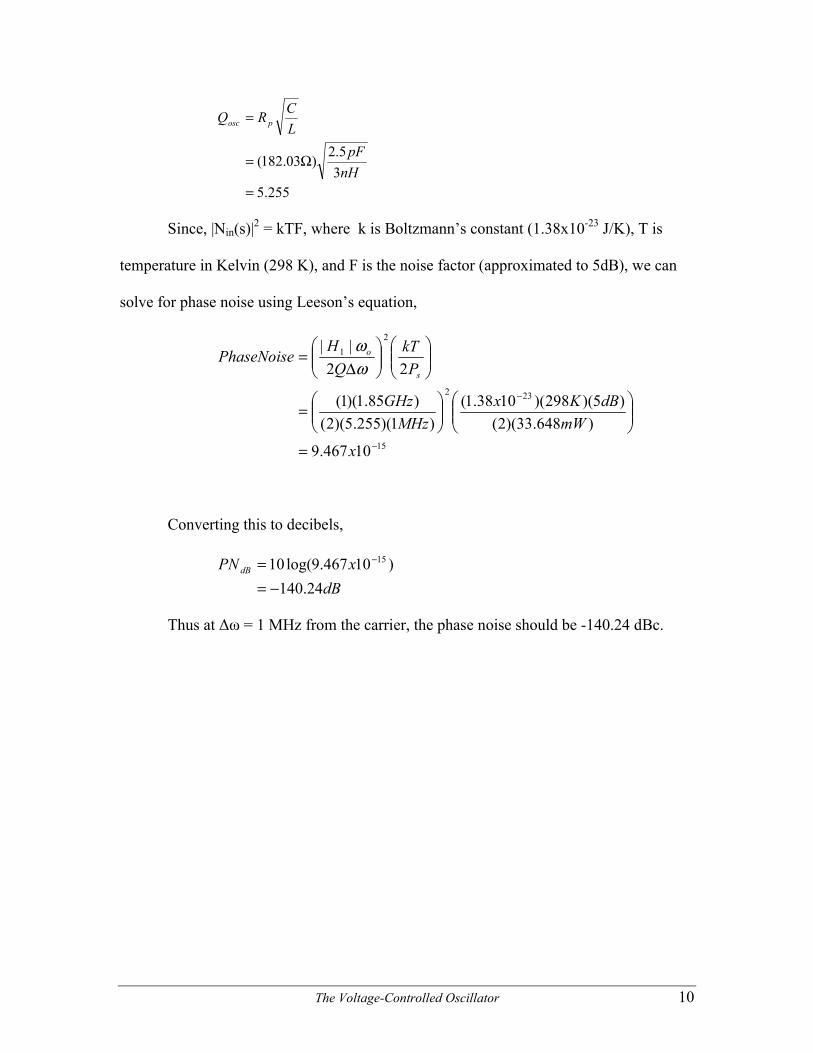
The Voltage-Controlled Oscillator 10
255.535.2
)03.182(
=
Ω=
=
nHpF
LCRQ posc
Since, |Nin(s)|2 = kTF, where k is Boltzmann’s constant (1.38x10⁻²³ J/K), T is
temperature in Kelvin (298 K), and F is the noise factor (approximated to 5dB), we can
solve for phase noise using Leeson’s equation,
15
232
21
10467.9
)648.33)(2()5)(298)(1038.1(
)1)(255.5)(2()85.1)(1(
22||
−
−
=
=
∆=
x
mWdBKx
MHzGHz
PkT
QH
PhaseNoises
o
ωω
Converting this to decibels,
dBxPN dB
24.140)10467.9log(10 15
−== −
Thus at ∆ω = 1 MHz from the carrier, the phase noise should be -140.24 dBc.

Oscillator Design Process 11
4.0 Oscillator Design Process
This section outlines the design process of the second voltage-controlled oscillator
(VCO). For simplicity, the design can be broken down into the following components:
• Oscillator topology
• LC resonator
• Varactors
• Inductors
• Polyphase Frequency shifter
Each component is described in detail in the following sections. Throughout the design,
emphasis was placed upon minimizing phase noise and power consumption and
maximizing tuning range, as these tend to be the most important characteristics of a
monolithic VCO [7].
4.1 The Negative Gm Oscillator The first course of action was to select an appropriate topology to base the design
of the oscillator upon. Though there are many common topologies available, such as the
Hartley or the Colpitts oscillator, the negative transconductance (gm) oscillator was
selected because the design offers low phase noise and large amplitudes of oscillation [4].
The differential operation of this topology, in addition, also lowers the common mode
power and the substrate noise [7].
As illustrated below in Figure 4, the negative gm oscillator is comprised of an LC
resonator and a pair of cross-coupled transistors. The LC resonator formed by the
inductors and the capacitors set the oscillating frequency, while the cross-coupled

Oscillator Design Process 12
transistors create a negative resistance that sustains the oscillations. In addition, the
current, represented in Figure 4 by the ideal current source, sets the output voltage swing
of the oscillations. This provides a starting point for design.
Figure 4: Negative Gm Oscillator topology
4.2 LC Resonator
Comprised simply of a capacitance in parallel with an inductance as illustrated
below in Figure 5, the LC resonator produces the initial voltage oscillation in response to
an impulse and controls the oscillating frequency. By representing the response to the
impulse mathematically, the frequency of oscillation can be derived [1] to yield the
following property:

Oscillator Design Process 13
1osc LC
ω = (4)
To enable the voltage-controlled oscillator to tune the oscillations to the desired
frequency range, 1.82 GHz to 1.87 GHz in the case of the second VCO, the inductance
and the capacitance of the resonator must be carefully set. To obtain an oscillating
frequency of 1.82 GHz for the second VCO,
21
2
9
10647.7
)1082.1(21
−=
=
x
xLC
π
and, similarly, for 1.87 GHz, LC = 7.244x10⁻²¹.
To achieve these LC constants, the inductance of the resonator is set first. Since
maximizing the inductances reduces the relative phase noise by increasing the voltage
swing, it is desirable to make the inductance of the resonator as large as possible [5].
Larger inductances also inheritantly results in smaller capacitive values. This is desirable
since smaller capacitances means lower power consumption [7]. This value, however, is
limited by the self-resonant frequency of the inductor fres, and by the fact that with large
inductors, the required capacitance value will be almost achieved with the parasitic
capacitances alone. This would leave no room for the capacitor used to tune the
oscillating frequency [5]. As a result, the inductance of the resonator was set to 3nH.
Using a 3nH inductor, the required capacitance for an oscillating frequency of
1.82 GHz can now be calculated as follows from the LC constant:

Oscillator Design Process 14
pF
xx
LxC
549.2
10310647.7
10647.7
9
21
21
=
=
=
−
−
−
Similarly, a capacitance of 2.415 pF is required to set the frequency of oscillation to 1.87
GHz.
Figure 5 below illustrates the LC resonator:
Figure 5: The LC Resonator
This design, however, is not yet complete, as the above LC resonator uses ideal
inductors and fixed capacitors. In order to vary the frequency of oscillation, the fixed
capacitor must be replaced by variable capacitors, known as varactors. As calculated
above, these varactors must be able to vary between 2.415 pF and 2.549 pF. In addition,
since real inductors vary with frequency, more realistic inductor models must be created
to replace the ideal models of the simulator.
4.3 Varactors Variable capacitors or varactors are used to tune the frequency of the oscillator. A
MOS device, operating in accumulation mode and illustrated below in Figure 6, similar

Oscillator Design Process 15
to an NMOS transistor with its source and drain connected, accomplishes this by
exploiting the natural capacitance between the gate and the substrate.
Figure 6: Cross-Section of a Varactor
With the “source” and “drain” terminals at the same potential, no current flows in the
depletion region of the transistor. Thus, as the gate voltage is increased, the depletion
region increases, in turn increasing the effective distance between the gate and the
substrate. This, in turn, acts as a parallel plate capacitor. As illustrated by the following
equation [3],
dAC roεε= (5)
the capacitance of a parallel plate capacitor is inversely dependent upon the distance
between the plates. Thus, as the gate voltage increases, the distance between the gate and
the substrate increases causing a decrease in the capacitance.
In order to design the varactors to meet the tuning requirements of the second
VCO, a test bench, illustrated in Figure 7 below, was created to test the varactors.

Oscillator Design Process 16
Figure 7: Varactor Test Bench
By running an s-parameter simulation on the above test bench and observing the
S11 response, the input impedance (both real and imaginary components) could be
determined as the tuning voltage Vtune was varied. The imaginary component of the input
impedance is the capacitive characteristic of the circuit and is represented by the
following relationship:
min
1ImC
zω
= (6)
Based on varactors designed by Porret et al. [9] and Andreani et al. [10], the
varactors for the VCO were dimensioned to have a width of 2630 µm and a length of 0.5
µm. An s-parameter analysis was performed to obtain the following results:

Oscillator Design Process 17
Figure 8: Smith Chart of Varactor’s Input Impedance
From Figure 8 above, the normalized impedance was found to be 0.7242 at 0V
and 0.6889 at 3V. Since the test bench had zo = 50 Ω, the capacitance of the varactors
can be calculated. At 1.82 GHz, the capacitance Cmin is determined as follows:
210.36)7242.0)(50(
~ImIm
=Ω=
= zzz o
since,

Oscillator Design Process 18
min
1ImC
zω
=
pFGHz
C
415.2)210.36)(82.1(2
1min
=
=π
In a similar fashion, Cmax can be determined to be 2.549 pF. Since the varactors can vary
their capacitance between 2.415 pF and 2.549 pF for a given tuning voltage between 0
and 3 V, the specified swing in frequency of oscillation can be achieved.
To better illustrate this, the following figure, Figure 9, presents the capacitive
variation with respect to the changing tuning voltage.
Varactor Capacitance vs. Tuning Voltage
2.35
2.40
2.45
2.50
2.55
2.60
2.65
-2 -1 0 1 2 3 4 5
Vtune (V)
Capa
cita
nce
(pF)
Figure 9: Normalized Imaginary Impedance vs. Tuning voltage of Varactors

Oscillator Design Process 19
4.4 Inductors
The phase noise in a voltage-controlled oscillator is primarily dependent upon the
quality factor of the LC resonator [8]. Since a high quality factor (Q) is achievable for
MOS varactors [9], the inductor is generally the source of the majority of the phase noise
in the circuit. The quality factor of an inductor is defined by the following equation [1]:
LR
ZZQ
p
ind
indind
ω=
=|)Re(||)Im(|
(7)
(8)
As illustrated by the above equation, inductors with a high Q have very small
parallel resistances associated with them and, consequently, less phase noise. Real
inductors, however, tend to have much larger resistive properties and, thus, exhibit a
significantly lower Q. On chip inductors, unfortunately, exhibit even lower values of Q;
however, trends towards large-scale integration, lower costs, and lower power
consumption have motivated much research and study [8].
From the definition of the quality factor Q above, it can also be observed that the
Q of an inductor depends on the frequency of operation ω. This relationship however is
not a linear one for all frequencies of operation. Care must be taken when designing an
inductor to ensure that the frequency of operation does not exceed the self-resonance
frequency fres of the inductance, the point at which the coil can no longer be used as an
inductor [8].
To ensure that the inductor achieves the desired inductance, self-resonance
frequency, and sufficiently high Q, the following guidelines [8] were observed
throughout the design of the inductor.
Oscillator Design Process 20
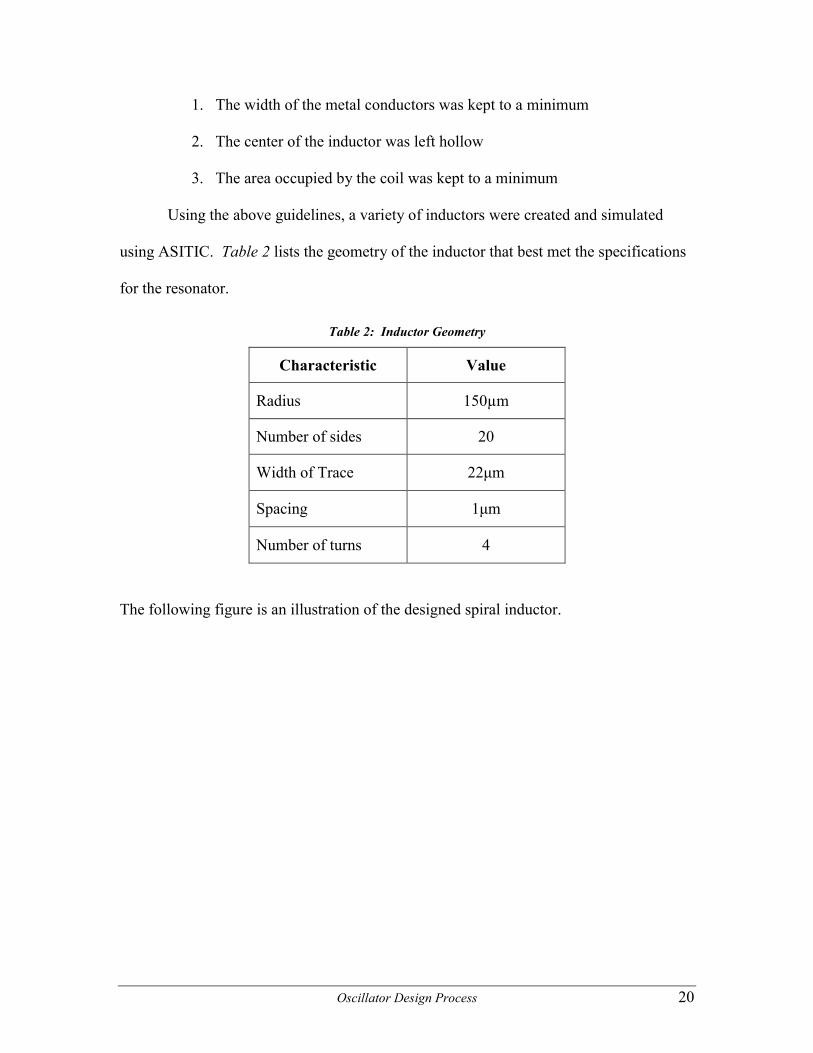
1. The width of the metal conductors was kept to a minimum
2. The center of the inductor was left hollow
3. The area occupied by the coil was kept to a minimum
Using the above guidelines, a variety of inductors were created and simulated
using ASITIC. Table 2 lists the geometry of the inductor that best met the specifications
for the resonator.
Table 2: Inductor Geometry
Characteristic Value
Radius 150µm
Number of sides 20
Width of Trace 22µm
Spacing 1µm
Number of turns 4
The following figure is an illustration of the designed spiral inductor.

Oscillator Design Process 21
Figure 10: Inductor Geometry
Using a pi model simulation in ASITIC, the following operating points for this inductor
were determined at 1.85 GHz, as indicated in the following table:
Table 3: Inductor Properties at 1.85 GHz
Characteristic Value
Inductance, L 3.01 nH
Quality Factor, Q 5.22
Self-Resonance Frequency, fres
4.52 GHz
Parallel Resistance, Rp 182.03 Ω

Oscillator Design Process 22
4.5 Polyphase Filters
As illustrated in Figure 2, the second voltage-controlled oscillator provides two
reference tones to the image reject mixers. Each signal is at a frequency of 1.85 GHz, but
one signal is 90 degrees out of phase from the other. This enables rejection of the image
signal when the two signals are added together.
To implement this 90 degree phase shift, a polyphase filter is used because of its
tolerance for component variations and improved performance over a wider range of
frequencies [1]. The polyphase filter consists of a number of stages of RC networks,
designed so that at a certain frequency all outputs are 90 degrees out of phase with each
other. With each additional stage, the phase shifts become increasingly closer to 90
degrees. Typically, due to economic reasons, the number of stages is kept to a limit of
four [11].
With the capacitors set to 100 pF, the resistor values were determined to be
1.162Ω from the following equation [1]:
RC1=ω (9)
Figure 11 below illustrates the 3-stage polyphase filter implemented for this
project.

Oscillator Design Process 23
Figure 11: 3-Stage Polyphase Filter
To test the designed polyphase filter, the testbench illustrated below in Figure 12,
was created and simulated. Below, a 1.85 GHz sinusoid is input into the polyphase filter.
The signal into port C is 180 degrees behind port A.
Figure 12: Polyphase Filter Testbench

Oscillator Design Process 24
The polyphase filter worked as expected as illustrated in Figure 13 by the output
signals obtained from port’s I and Q. The time difference between the peaks of each
output signal was measured to be 132.95 ps. Since a 1.85 GHz signal has a period of
540.54 ps, the phase shift can be calculated as follows,
°=°=
°
=
545.88360)24595.0(
36054.54095.132
x
xpspsPhaseShift
Figure 13: Polyphase Filter Testbench Output

Oscillator Design Process 25
4.6 Design Summary Incorporating all of the components mentioned above, the following is the
schematic of the cross-coupled negative transconductance (gm) oscillator. Some biasing
circuitry has also been added.
Figure 14: Complete VCO

Simulations and Results 26
5.0 Simulations and Results This section presents the results of the simulations of the second oscillator. The
figure below captures the operating points of all the transistors and components.
Figure 15: VCO Operating Points

Simulations and Results 27
5.1 Transient Response
The transient response of the cross-coupled negative gm oscillator is illustrated
below for Vtune = 0 V.
Figure 16: Transient Output Signal for Vtune = 0V
From Figure 16 above, the period was measure to be 541.437ps. Since frequency
is the inverse of the period, the oscillating frequency can be calculated to be 1.847 GHz.
Similarly, with the tuning voltage at 3 V, the oscillating frequency was measured to be
1.882 GHz. The output amplitude is also observed to be about 3.5 V.
Simulations and Results 28
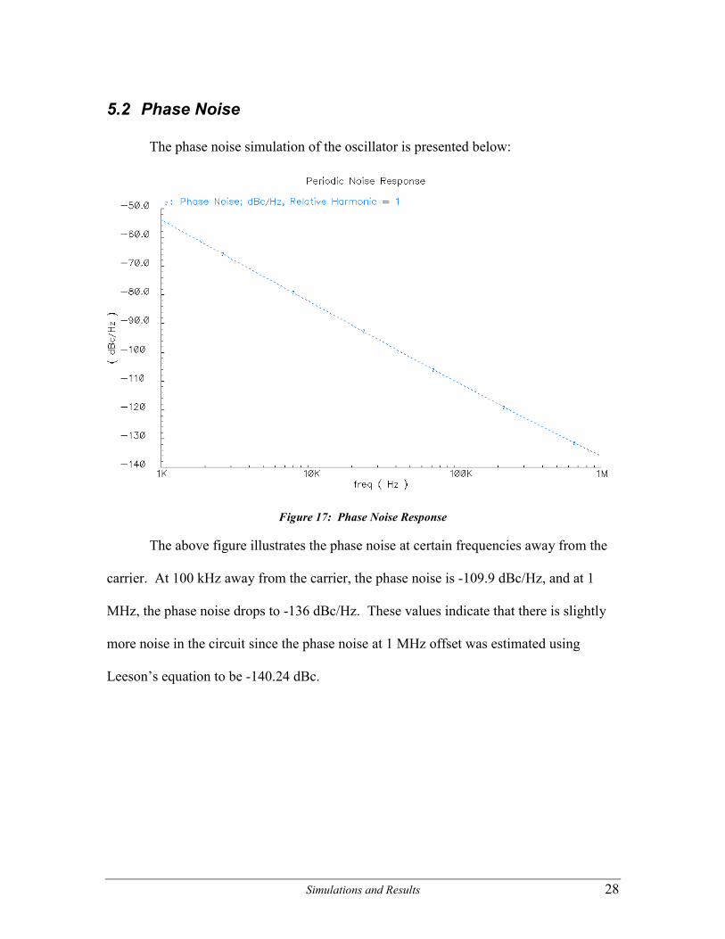
5.2 Phase Noise
The phase noise simulation of the oscillator is presented below:
Figure 17: Phase Noise Response
The above figure illustrates the phase noise at certain frequencies away from the
carrier. At 100 kHz away from the carrier, the phase noise is -109.9 dBc/Hz, and at 1
MHz, the phase noise drops to -136 dBc/Hz. These values indicate that there is slightly
more noise in the circuit since the phase noise at 1 MHz offset was estimated using
Leeson’s equation to be -140.24 dBc.

Simulations and Results 29
5.3 Results Summary The design results of the second voltage-controlled oscillator can be summarized
in the following table:
Table 4: Summary of Results
Characteristic Specification Result
Oscillating Frequency 1.82 GHz to 1.87 GHz 1.847 GHz to 1.882 GHz
Current Drain IBias ≤ 15 mA 15.39mA
Phase Noise at 100 kHz, PN ≤ -103 dBc/Hz at 1 MHz, PN ≤ -123 dBc/Hz
at 100 kHz, PN = -109.9 dBc/Hz at 1 MHz, PN = -136 dBc/Hz
An entirely monolithic voltage-controlled oscillator was successfully designed in
0.18µm CMOS to supply the image reject mixer with a stable, low-phase noise signal.
The oscillating frequency can be tuned between 1.847 GHz and 1.882 GHz by varying a
tuning voltage between 0V and 3V. Using a supply of 3.3 VDC, the circuit draws 15.39
mA of current and has phase noise of -109.9 dBc/Hz at a 100 kHz offset and -136 dBc/Hz
at a 1MHz offset from the carrier. This is meets the requirements specified at the start of
the project. To accomplish this, a spiral inductor was designed achieving a Q of 5.22.
MOS varactors were also implemented.
Lastly, a three stage polyphase frequency shifter was designed to create a signal
that was shifted by 90˚. This design resulted in a phase shift of 88.545˚.

Future Work 30
6.0 Future Work Unfortunately, due to computer difficulties beyond my control, I was unable to
run a DRC simulation, thus making layout impossible. In addition to layout, other
direction of future work could include modifying the existing design to meet the
requirements of the first voltage-controlled oscillator, specifically, increasing the tuning
range of the oscillator from 1.9 GHz to 2.7 GHz so that the VCO could be used to
provide the reference tone for the upconverting mixer. In addition, it might be interesting
to look at the design of the VCO using another technology such as BiCMOS or SiGe.
References 31
7.0 References [1] J. W. M. Rogers, C. Plett, Radio Frequency Integrated Circuit Design, Artech
House Inc, Boston. In Press.
[2] A. S. Sedra, K. C. Smith, Microelectronic Circuits, 1998, Oxford University
Press, NewYork.
[3] U. S. Inan, A. S. Inan, Engineering Electromagnetics, 1999, Addison-Wesley Inc,
California.
[4] J. W. M Rogers et al. “A Completely Integrated Cable Tuner”. SiGe
Semiconductors.
[5] B. Razavi. “A 1.8 GHz CMOS Voltage Controlled Oscillator”. IEEE ISSCC Dig.
Tech. Papers. 23:6. Feb 1997. (p 388-389).
[6] B. Razavi. “A Study of Phase Noise in CMOS Oscillators”. IEEE J. of Solid-
State Circuits. 31:3. March 1996. (p 331-343).
[7] F. Svelto, S. Deantoni, and R. Castello. “A 1.3 GHz Low-Phase Noise Fully
Tunable CMOS LC VCO”. IEEE J. on Solid-State Circuits. 35:3. March 2000.
(p 356-361).
[8] J. Craninckx and S. J. Steyaert. “A 1.8 GHz Low-Phase-Noise CMOS VCO
Using Optimized Hollow Spiral Inductors”. IEEE J. of Solid-State Circuits. 32:5.
May 1997. (p 736-744).
[9] A. Porret et al. “Design of High-Q Varactors for Low-Power Wireless
Applications Using a Standard CMOS Process”. IEEE J. of Solid-State Circuits.
35:3. March 2000. (p 337-345)

References 32
[10] P. Andreani and S. Mattison. “On the Use of MOS Varactors in RF VCO’s”.
IEEE J. of Solid-State Circuits. 35:6. June 2000. (p 905-910).
[11] M. J. Gingell. “Single Sideband Modulation using Sequence Asymmetric
Polyphase Networks”. Electrical Communications. 48. 1973. (p 21-25).


![LECTURE 130 – VOLTAGE-CONTROLLED …users.ece.gatech.edu/pallen/Academic/ECE_6440/Summer...LECTURE 130 – VOLTAGE-CONTROLLED OSCILLATORS (READING: [4,6,9]) Objective The objective](https://static.fdocuments.net/doc/165x107/5ac2dac57f8b9a357e8e7ae4/lecture-130-voltage-controlled-usersece-130-voltage-controlled-oscillators.jpg)