Voltage Balancing of DC Capacitors in Chain-Link...
132
Voltage Balancing of DC Capacitors in Chain-Link STATCOMs Jan Kheir Master of Engineering Electrical and Computer Engineering Department McGill University Montreal,Quebec 2014-07-23 A thesis submitted to McGill University in partial fulfillment of the requirements of the degree of Master of Engineering ©Jan Kheir, 2014
Transcript of Voltage Balancing of DC Capacitors in Chain-Link...
Voltage Balancing of DC Capacitorsin Chain-Link STATCOMs
Jan Kheir
Master of Engineering
Electrical and Computer Engineering Department
McGill University
Montreal,Quebec
2014-07-23
A thesis submitted to McGill University in partialfulfillment of the requirements of the degree of Master of Engineering
©Jan Kheir, 2014

ACKNOWLEDGEMENTS
I would like to thank Dr. Ambra Sannino for giving me the opportunity of
doing my thesis work in the R&D department at ABB FACTS. I would also like
to thank Mr. Greger Fasth who has made this possible by allowing me to share my
time between work and study. I would like to thank Mr. Mauro Monge and Mr.
Jean-Philippe Hasler. Their supervision and guidance has been essential. Finally,
I would like to thank professor Boon-Teck Ooi for accepting me as his student, and
for encouraging me from the very beginning.
ii

ABSTRACT
Modular Multilevel Converters (MMC) have become an interesting alternative
to other converter topologies for Static synchronous Compensator (STATCOM)
applications due to the modularity of their design and to their increased effective
switching frequency which reduces the harmonics on the AC side. The drawback
is that these converters have a large number of DC capacitors whose voltages have
to be controlled independently. This becomes particularly important when the
converter is required to operate during unbalanced conditions. The purpose of
this thesis is therefore to define the problem of DC capacitor voltage balancing in
MMC based STATCOMs, and to solve this problem for four different STATCOM
topologies. A comparison of the advantages and disadvantages of each converter
topology is then performed, and the proposed control schemes are implemented
and tested using Matlab/Simulink.
iii
ABREGE
Les convertisseurs modulaires multiniveaux (MMC - de l’anglais : Modu-
lar Multilevel Converter) deviennent une alternative interessante aux topologies
de convertisseurs conventionnelles pour des applications de compensateurs syn-
chrones statiques (STATCOM - de l’anglais : Static Synchronous Compensator)
grace, entre autres, a leur conception modulaire ainsi qu’a leur frequence effective
de commutation elevee qui reduit les harmoniques generees. L’inconvenient des
convertisseurs a topologie MMC est qu’ils comportent un grand nombre de con-
densateurs CC dont les tensions doivent etre controlees de facon independante.
Ceci devient particulierement important lorsque ces convertisseurs doivent operer
dans des conditions debalancees. L’objectif de cette these est donc de comprendre
le probleme qu’est le debalancement des tensions CC dans les STATCOM de type
MMC et de resoudre ce probleme pour quatre topologies differentes. Une compara-
ison des avantages et des inconvenients de chaque topologie de convertisseur sera
faite, et les algorithmes de controle developes seront realises et testes a l’aide de
Matlab/Simulink.
iv

TABLE OF CONTENTS
ACKNOWLEDGEMENTS . . . . . . . . . . . . . . . . . . . . . . . . . . . ii
ABSTRACT . . . . . . . . . . . . . . . . . . . . . . . . . . . . . . . . . . . iii
ABREGE . . . . . . . . . . . . . . . . . . . . . . . . . . . . . . . . . . . . . iv
LIST OF TABLES . . . . . . . . . . . . . . . . . . . . . . . . . . . . . . . . viii
LIST OF FIGURES . . . . . . . . . . . . . . . . . . . . . . . . . . . . . . . ix
LIST OF ABBREVIATIONS . . . . . . . . . . . . . . . . . . . . . . . . . . xii
1 Introduction . . . . . . . . . . . . . . . . . . . . . . . . . . . . . . . . . 1
2 STATCOM Principles and Applications . . . . . . . . . . . . . . . . . . 7
2.1 STATCOM Principles . . . . . . . . . . . . . . . . . . . . . . . . 72.2 STATCOM Applications . . . . . . . . . . . . . . . . . . . . . . 12
3 Voltage Source Converters . . . . . . . . . . . . . . . . . . . . . . . . . 14
3.1 Principles of a Basic Voltage Source Converter . . . . . . . . . . 143.2 Modular Multilevel Converter . . . . . . . . . . . . . . . . . . . 18
4 The Problem of DC Capacitor Voltage Balancing . . . . . . . . . . . . 21
5 Delta-Coupled Chain-Link STATCOM . . . . . . . . . . . . . . . . . . 26
6 Ungrounded Wye-Coupled Chain-Link STATCOM . . . . . . . . . . . 31
7 Grounded Wye-Coupled Chain-Link STATCOM . . . . . . . . . . . . . 34
8 Further Optimization to Increase STATCOM Output . . . . . . . . . . 40
8.1 Defining a Degree of Freedom . . . . . . . . . . . . . . . . . . . 408.2 The Optimization Problem . . . . . . . . . . . . . . . . . . . . . 438.3 Inequality Constraints . . . . . . . . . . . . . . . . . . . . . . . 438.4 Equality Constraints . . . . . . . . . . . . . . . . . . . . . . . . 438.5 Solution of the Problem . . . . . . . . . . . . . . . . . . . . . . 448.6 Example of Results With and Without the Optimization . . . . 44
v

9 Unbalance Between Cells in a Given Phase . . . . . . . . . . . . . . . . 47
10 Double Wye-Coupled Chain-Link STATCOM with Half-Bridge Cells . 49
11 Comparison of Chain-Link STATCOM Topologies . . . . . . . . . . . . 56
11.1 Delta-Coupled STATCOM . . . . . . . . . . . . . . . . . . . . . 5711.2 Ungrounded Wye-Coupled STATCOM . . . . . . . . . . . . . . 6011.3 Grounded Wye-Coupled STATCOM . . . . . . . . . . . . . . . . 6311.4 Double Wye-Coupled STATCOM . . . . . . . . . . . . . . . . . 6411.5 Summary of STATCOM Topology Comparison . . . . . . . . . . 64
12 Implementation of Control Strategies in Matlab/Simulink . . . . . . . . 65
12.1 Converter Modeling . . . . . . . . . . . . . . . . . . . . . . . . . 6512.2 STATCOM Controls . . . . . . . . . . . . . . . . . . . . . . . . 6712.3 DC Voltage Controls . . . . . . . . . . . . . . . . . . . . . . . . 68
12.3.1 Total Converter Average DC Voltage . . . . . . . . . . . 6912.3.2 Converter Leg Average DC Voltage . . . . . . . . . . . . 6912.3.3 Converter Cell Voltage . . . . . . . . . . . . . . . . . . . 72
13 Simulation Results . . . . . . . . . . . . . . . . . . . . . . . . . . . . . 74
13.1 Phase to Phase Fault with no STATCOM . . . . . . . . . . . . . 7413.2 Phase to Phase Fault with STATCOM (no DC voltage control) . 7613.3 Phase to Phase Fault with STATCOM (with DC voltage control) 7813.4 Test of Individual control loops . . . . . . . . . . . . . . . . . . 81
13.4.1 Total Converter Average DC Voltage Control Loop . . . . 8113.4.2 Test of PI based Converter Leg Average DC Voltage
Control Loop . . . . . . . . . . . . . . . . . . . . . . . 8213.4.3 Test of Predictive Converter Leg Average DC Voltage
Control Loop . . . . . . . . . . . . . . . . . . . . . . . 8313.4.4 Test of Converter Cell Voltage Control Loop . . . . . . . 84
13.5 Summary . . . . . . . . . . . . . . . . . . . . . . . . . . . . . . 85
14 Conclusion . . . . . . . . . . . . . . . . . . . . . . . . . . . . . . . . . . 86
15 Future Work . . . . . . . . . . . . . . . . . . . . . . . . . . . . . . . . 89
References . . . . . . . . . . . . . . . . . . . . . . . . . . . . . . . . . . . . . 90
A Symmetrical Components . . . . . . . . . . . . . . . . . . . . . . . . . 93
B Differential Mode and Common Mode Extraction for Scalar Quantities 97
vi

C Network Unbalances . . . . . . . . . . . . . . . . . . . . . . . . . . . . 100
C.1 Network Unbalances During Faults . . . . . . . . . . . . . . . . 100C.1.1 Grounded Network . . . . . . . . . . . . . . . . . . . . . 100C.1.2 Ungrounded Network . . . . . . . . . . . . . . . . . . . . 106
C.2 Network Unbalances During Normal Operation . . . . . . . . . . 113C.2.1 Transmission Line Unbalanced Impedances . . . . . . . . 113C.2.2 Unbalanced loads . . . . . . . . . . . . . . . . . . . . . . 116
C.3 Summary . . . . . . . . . . . . . . . . . . . . . . . . . . . . . . 116
D Active and Reactive Power Flow . . . . . . . . . . . . . . . . . . . . . 118
vii

LIST OF TABLESTable page
3–1 Valid switch combinations in a full-bridge VSC . . . . . . . . . . . . 15
11–1 Summary of STATCOM topology comparison . . . . . . . . . . . . . 64
C–1 Summary of Voltage Unbalances Due to Faults . . . . . . . . . . . . 117
viii

LIST OF FIGURESFigure page
2–1 Two bus network with active/reactive power flow . . . . . . . . . . 7
2–2 Typical STATCOM single-line diagram . . . . . . . . . . . . . . . . 8
2–3 Simple STATCOM control scheme for positive sequence voltagecontrol . . . . . . . . . . . . . . . . . . . . . . . . . . . . . . . . 9
2–4 Simple Phase-Locked Loop . . . . . . . . . . . . . . . . . . . . . . 10
3–1 Single-phase, full-bridge voltage source converter . . . . . . . . . . 15
3–2 SPWM for a full-bridge bipolar switching VSC . . . . . . . . . . . . 16
3–3 SPWM for a full-bridge uni-polar switching VSC . . . . . . . . . . . 17
3–4 Modular Multilevel Converter based chain-link VSC . . . . . . . . . 18
3–5 SPWM for a full-bridge uni-polar switching MMC chain-link VSCusing three cells . . . . . . . . . . . . . . . . . . . . . . . . . . . . 19
5–1 Delta-Coupled Chain-Link STATCOM . . . . . . . . . . . . . . . . 26
6–1 Ungrounded Wye-Coupled Chain-Link STATCOM . . . . . . . . . . 31
7–1 Grounded Wye-Coupled Chain-Link STATCOM . . . . . . . . . . . 34
8–1 Optimization of leg currents using common mode active power flow 45
10–1 Un-grounded Double Wye-Coupled Chain-Link STATCOM . . . . . 50
11–1 Legend for interpreting phasor diagrams . . . . . . . . . . . . . . . 57
11–2 Phase Voltages and Positive Sequence Leg Currents in a Delta-Coupled STATCOM During a Phase to Phase Fault . . . . . . . 58
11–3 Phase Voltages and Positive Sequence Leg Currents in a Delta-Coupled STATCOM During a Phase to Phase Fault with ZeroSequence Current Injection . . . . . . . . . . . . . . . . . . . . . 59
ix

11–4 Phase Voltages and Positive Sequence Leg Currents in a Wye-Coupled STATCOM During a Phase to Phase Fault with ZeroSequence Voltage Injection . . . . . . . . . . . . . . . . . . . . . 60
11–5 Positive Sequence Phase Voltages and Unbalanced Leg Currents ina Wye-Coupled STATCOM . . . . . . . . . . . . . . . . . . . . . 61
11–6 Positive Sequence Phase Voltages and Unbalanced Leg Currents ina Wye-Coupled STATCOM with Zero Sequence Voltage Injection 62
11–7 Positive Sequence Phase Voltages and Unbalanced Leg Currents ina Delta-Coupled STATCOM with Zero Sequence Current Injection 63
12–1 Test circuit used in Matlab/Simulink simulations . . . . . . . . . . . 65
12–2 Simplified test circuit used in Matlab/Simulink simulations . . . . . 66
12–3 Modeling of converter cells as controllable voltage sources . . . . . . 66
12–4 Full controls of the STATCOM . . . . . . . . . . . . . . . . . . . . 68
12–5 Control loop for total converter average DC voltage . . . . . . . . . 69
12–6 Predictive control loop for converter leg average DC voltage . . . . 70
12–7 PI control loop for converter leg average DC voltage . . . . . . . . . 71
12–8 Control loop for converter cell voltage (phase a) . . . . . . . . . . . 72
13–1 Sequence voltages (STATCOM inactive) . . . . . . . . . . . . . . . 75
13–2 Phase voltages and currents (STATCOM inactive) . . . . . . . . . 75
13–3 Sequence voltages (STATCOM active but no DC voltage control) . 76
13–4 Phase voltages and currents (STATCOM active but no DC voltagecontrol) . . . . . . . . . . . . . . . . . . . . . . . . . . . . . . . . 77
13–5 Cell voltages (STATCOM active but no DC voltage control) . . . . 78
13–6 Sequence voltages (STATCOM active and DC voltage control enabled) 79
13–7 Phase voltages and currents (STATCOM active and DC voltagecontrol enabled) . . . . . . . . . . . . . . . . . . . . . . . . . . . . 80
13–8 Cell voltages (STATCOM active and DC voltage control enabled) . 80
13–9 Cell voltages after a step in total converter avg. DC voltage reference 81
13–10 Cell voltages (PI controller for leg avg. DC voltage disabled) . . . 82
x

13–11 Cell voltages (Predictive leg avg. DC voltage controller disabled) . 83
13–12 Unbalanced cell voltages within the same phase (phase A) . . . . 85
A–1 Symmetrical components . . . . . . . . . . . . . . . . . . . . . . . . 93
C–1 Grounded Net . . . . . . . . . . . . . . . . . . . . . . . . . . . . . . 101
C–2 Phase voltages during a single phase to ground fault in phase a . . 102
C–3 Phase voltages during a two phase to ground fault in phases a and b 103
C–4 Phase to Phase fault in a grounded network . . . . . . . . . . . . . 104
C–5 Phase voltages during a phase to phase fault between phases b and c 105
C–6 Ungrounded Network . . . . . . . . . . . . . . . . . . . . . . . . . . 107
C–7 Phase voltages during a single phase to ground fault in phase a . . 108
C–8 Two-Phase to Ground Fault in an Ungrounded Network . . . . . . . 109
C–9 Phase voltages during a two phase to ground fault in phases a and b 110
C–10Phase voltages during a phase to phase fault between phases b and c 112
C–11Typical three-phase transmission line . . . . . . . . . . . . . . . . . 114
D–1 Transmission line and active/reactive power flow . . . . . . . . . . 118
xi

LIST OF ABBREVIATIONS
AC: Alternating Current
DC: Direct Current
FACTS: Flexible Alternating Current Transmission Systems
HVDC: High Voltage Direct Current
IGBT: Integrated Gate Bipolar Transistor
KCL: Kirchhoff’s Current Law
KVL: Kirchhoff’s Voltage Law
MMC: Modular Multilevel Converter
PI: Proportional-Integral
PLL: Phase Locked Loop
PWM: Pulse Width Modulation
SPWM: Sinusoidal Pulse Width Modulation
STATCOM: Static Synchronous Compensator
SVC: Static var Compensator
TCSC: Thyristor Controlled Series Capacitor
VSC: Voltage Source Converter
xii

CHAPTER 1Introduction
With the ever increasing need for energy, many power transmission networks
are reaching their limits. Building new transmission lines could possibly alleviate
this problem, but the associated cost is extremely high, and the level of urbanization
in many regions often makes this impossible. One possible solution is to optimize
existing networks.
Given that networks need a stability margin in order to cope with transient
events, the power transmission capabilities cannot be increased up to the thermal
limits of lines and transformers. However, if the size and severity of these tran-
sient events can be reduced, the necessary margin can also be reduced, and more
transmission capability can be obtained from the same network.
Several devices can be used in order to improve network transient stabiliy.
One such device is the Static Synchronous Compensator or STATCOM as it will
be referred to from here on. In addition to improving network transient stability,
STATCOMs can also be used for voltage support and to improve power quality
in many industrial processes. Utilities impose strict power quality requirements
on industries, and the costs associated with the penalties for not fulfilling these
requirements are quite high. Therefore, STATCOMs are often a worthwhile invest-
ment for large industrial customers.
1
2
For these reasons, much research in the field of STATCOM technologies has
occured in the last decades, and the arrival of new converter topologies has gen-
erated new challenges and created the need for more sophisticated control strate-
gies. One of these innovations has been the advent of modular multilevel convert-
ers (MMC). MMC based topologies have many advantages over other converter
topologies, namely the modularity of the design, but also the increased effective
switching frequency which reduces the harmonics on the AC side. However, this
modularity comes at a cost: The increased complexity of the system requires more
sophisticated controls.
One of the main differences with MMC based converters is that they are com-
posed of many modules or cells which each have a DC capacitor. This means
that several DC voltages need to be controlled. For a STATCOM application un-
der normal conditions with balanced phase voltages and currents, the converter
provides only reactive power. However, in unbalanced conditions, the converter
will supply/absorb unbalanced active power. In other words, each phase will sup-
ply/absorb a different amount of active power. This flow of active power changes
the DC capacitor voltages, and this is of course not sustainable. The purpose of
this thesis is therefore to define the problem of DC capacitor voltage balancing in
MMC based STATCOMs, and to solve this problem for four different STATCOM
topologies. A comparison of the advantages and disadvantages of each converter
topology is then performed.
Chapters 2 and 3 of this thesis are dedicated to giving a brief overview of the
basic purpose of STATCOMs as well as the operating principles of Voltage Source
Converters (VSCs).
Chapter 4 presents a detailed explanation of the problem of capacitor DC
voltage balancing. The flow of active power into the STATCOM legs is separated
3
into common mode active power flow and differential mode active power flow. It is
then explained that the common mode active power flow can be easily controlled
by setting the correct angle between the positive and negative sequence current
references and the positive and negative sequence voltages present on the network.
The control of differential mode active power flow requires additional controls which
are specific to the converter topology. The subsequent chapters describe the four
STATCOM topologies which are studied in this thesis, and the applicable methods
for differential mode active power flow control are developed.
One solution applicable to all topologies that are evaluated in this thesis is to
control the voltage of each cell locally. This is done by comparing the cell voltage to
a reference, and modifying the switching pattern of each cell in order to change the
time during which each cell is conducting. By doing so, it is possible to control the
average energy absorption of each cell over a switching cycle and therefore control
the voltage of each cell. Such methods are for example described in [18], [21]
and [22]. A similar method is used in this thesis and is described in chapter 9 and
in section 12.3.3. The difference is that in this thesis, localized control for each
cell is not the only method used. It is used as part of a scheme of nested control
loops. The reason is that these localized methods rely on the detection of an error
in DC voltage. The additional control loops used here rely on measured network
voltages and STATCOM currents in order to anticipate DC voltage drift caused
by unbalanced operation. These methods anticipate the error and take corrective
measures in order to prevent it. They are therefore different from methods which
rely on the detection of an error.
These additional methods are however dependant on the converter topology.
For a single wye-coupled or delta-coupled converter supplying positive sequence

4
currents to a network with unbalanced voltages, it is possible to impose a negative-
sequence current that will cancel the flow of active power. Such methods are used,
for example, in [5], [14] and [20]. This is not a preferred solution as the negative
sequence currents increase the unbalance condition in the network. Furthermore,
this method imposes a restriction on the operating range of the STATCOM. Indeed,
it is not possible to provide any wanted positive sequence currents and negative
sequence currents simultaneously as they are related by the need to cancel active
power flow.
Chapter 6 presents another solution for the wye-coupled converter which is
to impose a zero-sequence voltage on the neutral point of the converter. Such a
method is presented in [19]. A similar method is developed in this thesis, with
the difference that the calculation of the zero sequence voltage is simplified. This
method does not create additional unbalance in the network, and is flexible in the
sense that positive-sequence currents and negative sequence currents can be chosen
somewhat independently. It can be shown that it is not always possible to find
a finite zero-sequence voltage that will cancel the flow of active power if both a
negative sequence current and a positive sequence current need to be supplied.
Furthermore, this method requires that the converter be rated for a much higher
voltage than the nominal system voltage.
Chapters 5 and 7 present the methods applicable to a delta-coupled converter
or a wye-coupled converter with a neutral current path respectively. Both of these
methods are based on the use of a zero-sequence current. A similar method to the
ones which are developed in these chapters are also described in [4], [5] and [20]
but again, the method presented for calculating the zero-sequence current reference
produced by the converter assumes balanced leg currents, and is therefore not a
general method. Moreover, the methods presented in this thesis are developed

5
based on the calculation of a differential power vector which is simpler and less
cumbersome than the method described in [4], [5] and [20]. The zero-sequence
current method does not require the converter to be overrated from a voltage
perspective, however, it does require a higher current rating. It can also be shown
for this method that it is not always possible to find a finite zero-sequence current
that will cancel the flow of active power if both a positive sequence voltage and a
negative sequence voltage are present in the network. This method also relies on
the existence of a zero-sequence current path which requires the use of additional
components such as a grounding transformer in the case of a wye-coupled converter.
Chapter 8 then explains how the exchange of common mode active power flow
between the positive sequence and the negative sequence can be used in order to
minimize the STATCOM leg currents and effectively increase the available reactive
power output of the converter.
Chapter 9 gives a brief explanation of one more cause of DC capacitor unbal-
ance which is the drift of cell DC voltages due to the non-ideal nature of components
and switching patterns. A solution to this problem based on individual control of
each cell is presented. This method is applicable regardless of the converter topol-
ogy, and is used in conjunction with the common mode active power control and
the differential mode active power control. Other methods such as selective swap-
ping are described in [12]. The advantage of the method presented in this thesis
is that it can be implemented locally for each cell and does not require centralized
control.
Chapter 10 presents a fourth converter topology. This converter is composed
of two wye-coupled converters with their neutral points connected together (or
not). This type of converter configuration is used in the latest non-traditional
HVDC applications [9]. A control scheme for DC capacitor voltage balancing is

6
presented in [13], but this control scheme requires the existence of a path for neutral
current. In this thesis, it is shown that for this converter configuration, all methods
described previously are applicable, but there also exists another method. Indeed,
it is possible to use DC currents to cancel the active power flow. Due to the fact
that this method relies on DC quantities, it can be shown that there always exists
a finite solution that will cancel the active power flow. However, it also requires
a converter with a higher current rating. It will also be shown how combining
these methods may result in a reduction of the converter stresses. However, due to
its topology the double-wye coupled converter requires more leg reactors and DC
capacitors than the single wye-coupled converter, and is therefore more expensive
and has a larger footprint.
Chapter 11 presents a brief comparison of the advantages and disadvantages
of each of the converter topologies. The comparison is mainly done on the basis of
limitations of the operating ranges due to the necessity of balancing DC voltages.
The cost and complexity of each topology are also briefly mentioned.
Chapter 12 presents one proposed implementation of the methods described
above for a simple STATCOM containing three cells per phase. This implementa-
tion is directly scalable for a converter with more cells.
Chapter 13 presents the results of simulations which were performed in order
to validate that the DC voltage control methods function correctly.

CHAPTER 2STATCOM Principles and Applications
The STATCOM, is one member of the large family of Flexible AC Transmission
Systems Controllers (FACTS Controllers). In simple terms, the STATCOM is a
shunt device which acts as a voltage source by controlling the amount of reactive
power it absorbs or generates. This chapter briefly explains what STATCOMs are
used for, and how they operate from a system point of view.
2.1 STATCOM Principles
Starting from a two bus network such as the one shown in figure 2–1, one can
derive the following equations for active and reactive power flow. The derivation
sV
rVI
LX
Figure 2–1: Two bus network with active/reactive power flow
is presented in appendix D and assumes that the angle between the sending end
voltage and the receiving end voltage δ is small.
Pr ≈ −VrVsδ
XL
(2.1)
Qr ≈VrVsXL
− V 2r
XL
=Vr(Vs − Vr)
XL
(2.2)
As demonstrated by equation (2.2), if one assumes that Vs is constant, then chang-
ing Qr will mainly have an impact on Vr. In the network of figure 2–1, the
7

8
impedance XL can be split into two parts. The first part can represent a Thevenin
equivalent network together with the source Vs, and the second part can represent
the combined transformer reactance and phase reactance of a STATCOM where
the source Vr represents the converter. A schematic of a STATCOM is shown in
figure 2–2. If the system is taken in per-unit, the transformer leakage inductance is
V
convV
I
phX
trX
Figure 2–2: Typical STATCOM single-line diagram
lumped with the phase inductance of the STATCOM to form Xstat. If pure reactive
power flow is assumed, the following relations can then be stated:
I =V − VconvXstat
(2.3)
Q =1− Vconv
V
Xstat
V 2 (2.4)
If Vconv is larger than V , the reactive power becomes negative and the STATCOM
is therefore behaving as a capacitor. On the other hand, if Vconv is smaller than
V , the reactive power becomes positive and the STATCOM is then behaving as a

9
reactor. In reality, a small amount of active power can flow into the STATCOM
under certain conditions, and this will be dealt with in the subsequent chapters.
A simple control scheme is presented in figure 2–3 to control the positive
sequence voltage at the STATCOM busbar. The busbar voltages are measured and
Figure 2–3: Simple STATCOM control scheme for positive sequence voltage control
transformed to the αβ0 reference frame by applying the following transformation:~Vα
~Vβ
~V0
=2
3
1 −1
2−1
2
0√32−√32
12
12
12
~Va
~Vb
~Vc
(2.5)
This transformation is also called the Clarke transformation [6], and for reference
purposes, the inverse Clarke transformation is:~Va
~Vb
~Vc
=
1 0 1
−12
√32
1
−12−√32
1
~Vα
~Vβ
~V0
(2.6)
The Clarke transformation is basically a projection of the three-phase quantities
onto two orthogonal axes where the α axis is in phase with phase a of the rotating
three-phase system.

10
In order to obtain the positive sequence voltage and the d-q frame so as to
implement the controls, it is necessary to acquire the argument θ = ωt + φ of the
a-phase voltage. Along the upper path of figure 2–3, the a-b-c frame voltages are
transformed to the αβ0 frame using equation 2.5 and then passed to the Phase
Locked Loop (PLL) of figure 2–4 which acquires the argument θ = ωt + φ. The
design of a phase-locked loop is fairly complex in the sense that its behaviour must
be optimized according to several design criteria such as the desired response time,
the range of frequencies to which it must be able to latch on to, the behavior in the
presence of a negative sequence component as well as the behavior in the presence
of harmonics to name a few. A simple phase-locked loop is shown in figure 2–4.
Once the angular position θ is extracted by the PLL, it is used to reconstruct the
Figure 2–4: Simple Phase-Locked Loop
positive sequence voltage component of the phase voltages. This is simply done by
implementing the following equation:
va1(t) = V1sin(θ) (2.7)
vb1(t) = V1sin(θ − 2π3
) (2.8)
vc1(t) = V1sin(θ − 4π3
) (2.9)

11
In parallel to this, the phase voltages are also transformed into their sequence
components using the following equation.~V0
~V1
~V2
=1
3
1 1 1
1 a a2
1 a2 a
~Va
~Vb
~Vc
(2.10)
where a is equal to ej2π3 .
Equation (2.10) is derived in Appendix A. For a STATCOM application of
positive sequence voltage support such as the one described here, the magnitude
of the positive sequence current is computed based on the difference between the
measured positive sequence voltage magnitude and the desired reference. The
currents are computed in the dq0 reference frame and then transformed into the abc
reference frame using equation 2.12 which is the inverse of the dq0 transformation.
The dq0 transformation is:Id
Iq
I0
=2
3
cos(θ) cos(θ − 2π
3) cos(θ − 4π
3)
−sin(θ) −sin(θ − 2π3
) −sin(θ − 4π3
)
12
12
12
Ia(t)
Ib(t)
Ic(t)
(2.11)
and the inverse of the dq0 transformation is:Ia(t)
Ib(t)
Ic(t)
=
cos(θ) −sin(θ) 1
cos(θ − 2π3
) −sin(θ − 2π3
) 1
cos(θ − 4π3
) −sin(θ − 4π3
) 1
Id
Iq
I0
(2.12)
The dq0 is also a projection of the three-phase quantities onto two orthogonal axes
where the d and q axes are orthogonal to each other, but this time they rotate at
the same angular velocity θ = ωt as the three-phase quantities. The d axis is in
phase with phase a of the three-phase system at t = 0 and at every cycle. One

12
reason for using a current reference in the dq0 reference frame is that by using the
angle θ = ωt of the three-phase voltages produced by the PLL, the d component of
the current then corresponds to a three-phase quantity which is in phase with the
three-phase voltages. Similarly, the q component of the current corresponds to a
three-phase quantity in quadrature with the three-phase voltages. In the dq frame,
the active and reactive power are therefore:
P = VdId + VqIq (2.13)
Q = VdIq − VqId (2.14)
When the PLL is locked on to phase a, Vq = 0. Therefore:
P = VdId (2.15)
Q = VdIq (2.16)
In other words, the d component of the current carries only active power whereas
the q component of the current carries only reactive power. Since the desired oper-
ation of the STATCOM is to exchange only reactive power with the network, the
reference current needed to support the positive sequence voltage should only have
a q component. Once the current reference is transformed from the dq0 reference
frame to a three-phase quantity, the measured phase currents are subtracted from
it, the result is scaled by a proportional gain, and then subtracted from the positive
sequence voltage which was reconstructed earlier. The result becomes the voltage
reference that the converter will follow.
2.2 STATCOM Applications
The uses for STATCOMs and shunt compensation in general are multiple. In
the context of transmission networks, they are often used for:

13
• End of line voltage support in order to prevent voltage instability. An exam-
ple of this would be for voltage support at a load center in the event of load
fluctuations or loss of one of several feeders.
• Improvement of transient stability, an example of which would be to provide
fast dynamic voltage support during faults in order to avoid loss of synchro-
nism of generators.
• Power oscillation damping in poorly damped power systems. Disturbances in
poorly damped networks will have the tendancy to create mechanical oscilla-
tions in the rotors of generators, thus changing the voltage angle and creating
oscillations in the active power transmitted.
In addition to the applications stated above, other applications exist which are
more specific to industrial processes. These include:
• Flicker compensation for loads with a very stochastic behavior. An example
of this would be flicker compensation for arc furnaces.
• Low order harmonic cancellation. STATCOMs being devices with a very fast
response time, they are capable of cancelling the first few harmonic orders
created by non-linear loads.
• Compensation of load unbalances. As will be seen in later chapters, STAT-
COMs are capable of generating unbalanced currents. This property can be
used to compensate for unbalanced three-phase loads.
Additional information and more detailed explanations about some of these appli-
cations can be found in [10], [15] and [16]. The following chapter explains how the
actual converter is implemented, and how it operates.

CHAPTER 3Voltage Source Converters
This chapter explains what a Voltage Source Converter is, and describes how
several of them can be connected to create a Modular Multilevel Converter (MMC).
3.1 Principles of a Basic Voltage Source Converter
The conventional thyristor, used in several FACTS devices such as the Static
Var Compensators(SVC) or the Thyristor-Controlled Series Capacitors (TCSC) can
be triggered to turn-on at any point on the half-cycle of voltage waveform during
which the device is positively biased. However, the turn-off cannot be controlled.
The device can only stop conducting once the current flowing through it goes to
zero. Other devices such as the Integrated Gate Bipolar Transistor (IGBT) have
both turn-on and turn-off capability. These devices therefore enable new converter
concepts which can have significant cost and performance advantages [17]. One
such converter type is the voltage source converter (VSC). The VSC concept can
be applied to single-phase or multi-phase converters using either half-bridges or
full-bridges. A single-phase, full bridge VSC is presented in figure 3–1. This
converter is presented here in more detail because it is the building block of the
STATCOMs which will be discussed in subsequent chapters. The VSC is composed
of one DC capacitor, one series AC reactor, as well as four switches and four anti-
parallel diodes. Since the DC voltage never changes polarities, anti-parallel diodes
are sufficient to ensure operation in all four power quadrants. The four switches
offer sixteen different on/off combinations. However, it is clear that closing both
switches of the same leg at the same time, that is 1 and 2 or 3 and 4, would result
in a short circuit across the capacitor which is of course undesireable. Eliminating
14

15
�
�
�
�
acV
Figure 3–1: Single-phase, full-bridge voltage source converter
all switch combinations which include two switches of the same leg being closed
at the same time, as well as all four combinations where only one switch is closed
(which are of no use), five combinations of interest remain. These combinations
are given in table 3–1. The last combination is valid, but is of no great interest
Table 3–1: Valid switch combinations in a full-bridge VSC
S1 S2 S3 S4 Voltage at terminals
1 0 0 1 +Vdc
0 1 1 0 −Vdc1 0 1 0 0
0 1 0 1 0
0 0 0 0 Open Circuit
since it simply results in the converter being idle. The other four combinations are
of more interest because by alternately changing between them, the voltage across
the VSC terminals can be made to follow an AC voltage reference. This is done
through the process of Sinusoidal Pulse Width Modulation (SPWM).
The full-bridge VSC can operate with two switching schemes; either bipolar
switching or uni-polar switching. Bipolar switching requires that diagonal switch
pairs always have the same state, meaning that the converter can only operate

16
using the two first switch combinations. Uni-polar switching on the other hand,
allows for the use of all four switch combinations.
The principle of SPWM is that the sinusoidal reference m(t) is compared to
a triangular waveform c(t) called the carrier. In the bipolar switching scheme,
when m(t) > c(t), switches 1 and 4 are on and switches 2 and 3 are off. When
m(t) < c(t), switches 1 and 4 are off and switches 2 and 3 are on. Assuming that
m(t),c(t)
−1
0
1
S1
0
1
S2
0
1
S3
0
1
S4
0
1
AC
Voltage
Time(s)
−Vdc
0
Vdc
0.000 0.004 0.008 0.012 0.016 0.020
Figure 3–2: SPWM for a full-bridge bipolar switching VSC
the DC capacitor is large enough so that the DC voltage remains constant, and
that the frequency of c(t) is much higher than that of m(t), the average of the AC
voltage over one switching period is equal to the duty cycle times the DC voltage.
This situation is illustrated in figure 3–2. In the unipolar switching scheme, the
on/off states of switches 1 and 2 are generated in exactly the same way as for the
bipolar switching scheme. The on/off states of switches 3 and 4 are generated by

17
comparing −m(t) with c(t). when −m(t) < c(t), switch 4 is on and switch 3 is off.
When −m(t) > c(t), switch 4 is off and switch 3 is on. This situation is illustrated
in figure 3–3. The major advantage of the uni-polar switching scheme over them(t),c(t)
−1
0
1
S1
0
1
S2
0
1
S3
0
1
S4
0
1
AC
Voltage
Time(s)
−Vdc
0
Vdc
0.000 0.004 0.008 0.012 0.016 0.020
Figure 3–3: SPWM for a full-bridge uni-polar switching VSC
bipolar scheme is that the generated waveform is a much better approximation to
the reference waveform. The result is much lower harmonic distortion.
It should be noted that although this converter allows four quadrant operation,
the flow of active power is restricted to exactly the amount necessary to replace
the converter losses and maintain the DC capacitor voltage. Indeed, since the
DC buses are not connected to a generator or load, a larger flow of active power
would result in a change in DC capacitor voltage. In this configuration, the VSC is
therefore more suitable for a STATCOM application since in this case, the converter
supplies/absorbs reactive power.
18
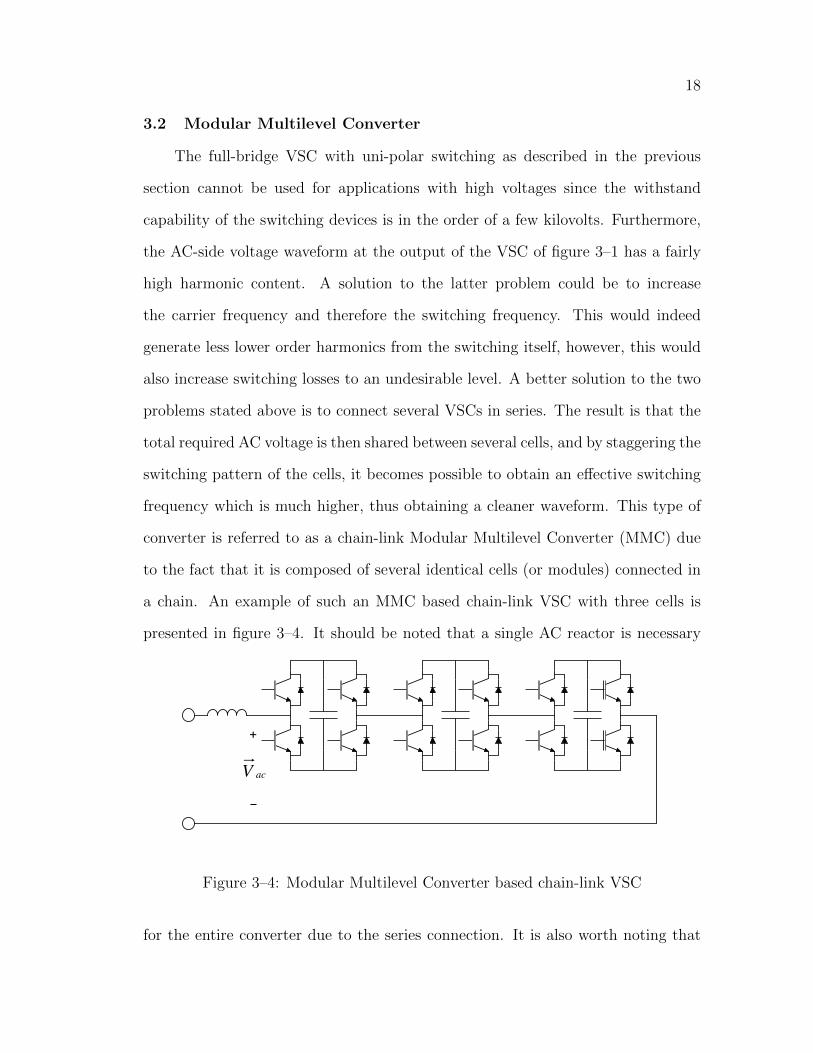
3.2 Modular Multilevel Converter
The full-bridge VSC with uni-polar switching as described in the previous
section cannot be used for applications with high voltages since the withstand
capability of the switching devices is in the order of a few kilovolts. Furthermore,
the AC-side voltage waveform at the output of the VSC of figure 3–1 has a fairly
high harmonic content. A solution to the latter problem could be to increase
the carrier frequency and therefore the switching frequency. This would indeed
generate less lower order harmonics from the switching itself, however, this would
also increase switching losses to an undesirable level. A better solution to the two
problems stated above is to connect several VSCs in series. The result is that the
total required AC voltage is then shared between several cells, and by staggering the
switching pattern of the cells, it becomes possible to obtain an effective switching
frequency which is much higher, thus obtaining a cleaner waveform. This type of
converter is referred to as a chain-link Modular Multilevel Converter (MMC) due
to the fact that it is composed of several identical cells (or modules) connected in
a chain. An example of such an MMC based chain-link VSC with three cells is
presented in figure 3–4. It should be noted that a single AC reactor is necessary
acV
Figure 3–4: Modular Multilevel Converter based chain-link VSC
for the entire converter due to the series connection. It is also worth noting that
19
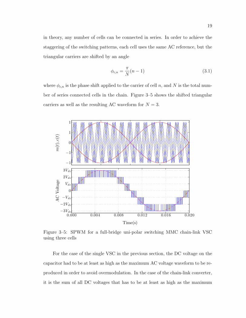
in theory, any number of cells can be connected in series. In order to achieve the
staggering of the switching patterns, each cell uses the same AC reference, but the
triangular carriers are shifted by an angle
φc,n =π
N(n− 1) (3.1)
where φc,n is the phase shift applied to the carrier of cell n, and N is the total num-
ber of series connected cells in the chain. Figure 3–5 shows the shifted triangular
carriers as well as the resulting AC waveform for N = 3.
m(t),c(t)
−1
−1
0
1
1
AC
Voltage
Time(s)
−3Vdc
−2Vdc
−Vdc
0
Vdc
2Vdc
3Vdc
0.000 0.004 0.008 0.012 0.016 0.020
Figure 3–5: SPWM for a full-bridge uni-polar switching MMC chain-link VSCusing three cells
For the case of the single VSC in the previous section, the DC voltage on the
capacitor had to be at least as high as the maximum AC voltage waveform to be re-
produced in order to avoid overmodulation. In the case of the chain-link converter,
it is the sum of all DC voltages that has to be at least as high as the maximum

20
AC voltage waveform to be reproduced. This clearly shows the suitability of the
MMC chain-link converter for high voltage applications. Not surprisingly, the total
number of voltage levels that can be reproduced is proportional to the number of
cells.
nlevels = 2N + 1 (3.2)
The AC waveform presented in figure 3–5 is a much better approximation to the
AC reference than the AC waveforms in figures 3–2 and 3–3. By increasing the
number of cells in a given converter, the harmonic content of the AC waveform
is reduced to a point where AC harmonic filters may no longer be required. The
following chapter will describe one of the problem which MMC based STATCOMs
are faced with when operating in unbalanced network conditions.
CHAPTER 4The Problem of DC Capacitor Voltage Balancing
The STATCOM described as a three phase voltage source in chapter 2 can
be constructed by using individual MMC-based VSCs such as the one shown in
figure 3–4 for each phase. Several different topologies can be acheived by connecting
the VSCs in different ways. For example, two of the simplest and more intuitive
topologies are the wye-coupled converters, where each phase of the STATCOM is
connected phase-to-ground, and the delta-coupled converters, where each phase of
the STATCOM is connected phase-to-phase. Variants of these topologies as well
as other topologies also exist. However, all of them suffer from the same problem
which is DC capacitor voltage unbalance. The present chapter will describe the
problem, and the subsequent chapters will present the main converter topologies
of interest as well as the applicable solutions for balancing these DC capacitor
voltages.
As explained earlier, except for the active power needed to replace the losses
in the converter, a STATCOM should only exchange reactive power with the net-
work. A larger (or smaller) exchange of active power would result in a change of
the DC voltages of the capacitors since these DC buses are floating. For now, and
until section 12.1, converter losses will be neglected in order to simplify the ex-
planation. Therefore, under normal operation in a network having only a positive
sequence voltage, it can be assumed that the STATCOM will generate a positive
sequence current which is either purely capacitive or purely inductive (or zero).
However, in unbalanced conditions such as those explained in appendix C, if, for
example, the STATCOM is to supply positive sequence reactive power, it will also
21

22
supply/absorb active and reactive power due to the product of positive sequence
current with negative sequence and zero sequence voltage. Furthermore, not only
will the STATCOM exchange active power with the network, but it will do so in
an unbalanced way. That is, the active power flowing in/out of each phase will be
different.
In order to quantify and understand how this occurs, let us first consider
the general case where STATCOM voltages and currents have positive sequence,
negative sequence and zero sequence components (“1”, “2” and “0” sub-indices).
~Va = ~Va0 + ~Va1 + ~Va2 (4.1)
~Vb = ~Vb0 + ~Vb1 + ~Vb2 (4.2)
~Vc = ~Vc0 + ~Vc1 + ~Vc2 (4.3)
~Ia = ~Ia0 + ~Ia1 + ~Ia2 (4.4)
~Ib = ~Ib0 + ~Ib1 + ~Ib2 (4.5)
~Ic = ~Ic0 + ~Ic1 + ~Ic2 (4.6)
The equations above use a simplified notation for the sequence components in each
phase quantity. For the full expression of each component, the reader may refer to
Appendix A. The active power flowing in each phase is the dot product of voltage
and current which gives
P = ~V · ~I (4.7)
= (~V0 + ~V1 + ~V2) · (~I0 + ~I1 + ~I2) (4.8)
= ~V0 · ~I0 + ~V0 · ~I1 + ~V0 · ~I2 + ~V1 · ~I0 + ~V1 · ~I1+
~V1 · ~I2 + ~V2 · ~I0 + ~V2 · ~I1 + ~V2 · ~I2 (4.9)

23
By applying the transformation developed in appendix B to equation 4.9 for all
three phases of the STATCOM, it is possible to identify the terms of equation 4.9
which result in a balanced flow of active power, and those which result in an
unbalanced flow of active power.x1,diff
x2,diff
xcomm
=1
3
2 −1 −1
−1 2 −1
1 1 1
Pa
Pb
Pc
(4.10)
The Pa, Pb and Pc are the expressions for active power flow into each phase as given
by equation 4.9. In equation 4.10, the xcomm term represents the common mode
power, that is, the power which is common to all three phases, whereas the x1,diff
and x2,diff terms represent together the differential mode power, that is, the power
which is unbalanced in all three phases. Similar methods for finding the common
mode and differential mode quantities of three phase variables are described in [8]
and [23]. Applying this to the product of positive sequence voltage and positive
sequence current,Pa11
Pb11
Pc11
=
Re{V1 6 (φV 1) · I1 6 (φI1)}
Re{V1 6 (φV 1 − 2π3
) · I1 6 (φI1 − 2π3
)}
Re{V1 6 (φV 1 − 4π3
) · I1 6 (φI1 − 4π3
)}
=
V1I1cos(∆φV 1I1)
V1I1cos(∆φV 1I1)
V1I1cos(∆φV 1I1)
(4.11)
we get the following expression for differential mode and common mode power.x1,diff
x2,diff
xcomm
=
0
0
V1I1cos(∆φV 1I1)
(4.12)

24
As expected, the product of positive sequence voltage and positive sequence current
gives only common mode power. Now, applying the same procedure to the product
of positive sequence voltage and negative sequence current,Pa12
Pb12
Pc12
=
Re{V1 6 (φV 1) · I2 6 (φI2)}
Re{V1 6 (φV 1 − 2π3
) · I2 6 (φI2 − 4π3
)}
Re{V1 6 (φV 1 − 4π3
) · I2 6 (φI2 − 2π3
)}
=
V1I2cos(∆φV 1I2)
V1I2cos(∆φV 1I2 + 2π3
)
V1I2cos(∆φV 1I2 − 2π3
)
(4.13)
we get the following expression for differential mode and common mode power.x1,diff
x2,diff
xcomm
=
V1I2cos(∆φV 1I2)
−V1I2(
12cos(∆φV 1I2) +
√32sin(∆φV 1I2)
)0
(4.14)
The product of positive sequence voltage and negative sequence current gives only
differential mode power. In fact, the previous analysis can be done for all the terms
in equation 4.9, and the result is that the product of same sequence voltages and
currents gives only common mode power whereas the product of different sequence
voltages and currents gives only differential mode power.
~V0 · ~I0~V1 · ~I1~V2 · ~I2
⇒ xcomm
~V0 · ~I1~V0 · ~I2~V1 · ~I0~V1 · ~I2~V2 · ~I0~V2 · ~I1
⇒ xdiff (4.15)
The common mode power terms cause a uniform change of capacitor voltage in all
phases. This situation can usually be prevented by properly defining the current

25
reference of the STATCOM so that all sequence currents are out of phase by ±π2
with respect to the voltages of the same sequence. The differential mode power
terms on the other hand, cause an unbalanced change of capacitor voltage in each
of the phases. Methods for preventing this situation depend on the configuration
of the converter, and will be the focus of the subsequent chapters.

CHAPTER 5Delta-Coupled Chain-Link STATCOM
The first topology that is of interest is the delta-coupled chain-link STATCOM.
The intent of this chapter is to describe this topology, and to solve the problem
of capacitor DC voltage balancing which is described in chapter 4 for this specific
topology. A schematic of the delta-coupled chain-link STATCOM is shown in
figure 5–1. By delta-coupled, it is implied that the VSCs are connected between
Figure 5–1: Delta-Coupled Chain-Link STATCOM
phases of a three-phase system. The voltage reference developed in figure 2–3 is
computed using phase to phase quantities, and is applied to the SPWM algorithm
of section 3.2 for all cells of the three phases of the STATCOM in figure 5–1.
The currents and voltages to consider in the calculation of the previous chapter
are of course the currents through the converter legs, and the voltages across them.
In the case of the delta-coupled STATCOM, the currents are therefore the currents
26

27
inside the delta, while the voltages are the phase to phase voltages. This means that
positive sequence, negative sequence and zero sequence currents can flow around
the delta, however, only positive sequence voltages and negative sequence voltages
are present across the legs since zero sequence voltages are eliminated due to the
delta-connection. Equation 4.9 therefore reduces to
P = ~V1 · ~I0 + ~V1 · ~I1 + ~V1 · ~I2+
~V2 · ~I0 + ~V2 · ~I1 + ~V2 · ~I2 (5.1)
Considering a case where the following positive and negative sequence voltages are
present while the STATCOM is providing positive sequence currents and negative
sequence currents,
~V1 = V1 6 φ1 (5.2)
~V2 = V2 6 φ2 (5.3)
it is possible to choose
~I1 = I1 6(φ1 ±
π
2
)(5.4)
~I2 = I2 6(φ2 ±
π
2
)(5.5)
in order to ensure that
~V1 · ~I1 = 0 (5.6)
~V2 · ~I2 = 0 (5.7)
However, it cannot be guaranteed in all conditions that
~V1 · ~I2 + ~V2 · ~I1 = 0 (5.8)

28
From equation 5.1 and from the fact that the STATCOM is delta-coupled, it is
interesting to notice that another degree of freedom is available. That is, a zero
sequence current reference can be imposed on the STATCOM which will not influ-
ence the phase currents outside the delta. However, inside the delta, this current
can be used to cancel the effect of the remaining unbalance terms. In other words,
the idea is to chose ~I0 so that
~V1 · ~I0 + ~V1 · ~I2 + ~V2 · ~I0 + ~V2 · ~I1 = 0 (5.9)
A different approach to the one developed here is used in [4] where an expression
for ~I0 is defined using space vectors for an application where a delta-coupled STAT-
COM is compensating for an asymmetrical load. This is a specific case where only
the differential power term ~V1 · ~I2 needs to be cancelled. However, the space vector
approach becomes somewhat cumbersome when trying to solve the general case
of equation 5.9. The power vector approach is more suitable for deriving a full
expression for ~I0 in the general case.
In order to solve for ~I0, equation 5.9 can be rewritten in the following form:
Re
~V1~I∗0
1
a2
a
+ ~V2~I∗0
1
a
a2
= −Re
~V1~I∗2
1
a
a2
+ ~V2~I∗1
1
a2
a
(5.10)
To obtain equation 5.10, equation 5.9 was expressed for each of the three phases,
and the terms were reorganised so that the three rows of equation 5.10 represent
the active power in each of the three phases. It is then possible to solve for ~I0.
Indeed, there are two unknowns which are the magnitude and the phase of the
zero sequence current. It is therefore required to solve two of the three rows of
equation 5.10. In other words, since equation 5.10 contains only differential mode
active power terms, if the active power flow is cancelled in two phases, it will
29
necessarily be zero in the third phase as well. Solving for example the first and
second rows, one gets:
I0 =(−V1I2sin(φ2,i − φ2) + V2I1sin(φ1,i − φ1)) sin(φ1 − φ2)
V1cos(φ1 − φ0) + V2cos(φ2 − φ0)(5.11)
φ0 = −arctan(V1 + V2cos(−3φ1 + 3φ2)
V2sin(−3φ1 + 3φ2)
)+ 2φ1 − φ2 (5.12)
The subscripts i in 5.11 denote that the angle in question is the angle of the current
phasor. The other angles are related to the voltage phasors. The latter equations
are valid only if sequence currents are orthogonal to the corresponding sequence
voltages as described in equations 5.2 to 5.5. Therefore, the first two sine terms in
the numerator of equation 5.11 simplify to ±1 depending if the sequence currents
are inductive or capacitive with respect the sequence voltages. In order to simplify
the notation here and in further chapters, the following quantities will be defined:
σ1 = I1sin(φ1,i − φ1) (5.13)
σ2 = I2sin(φ2,i − φ2) (5.14)
Equation 5.11 then become:
I0 =(−V1σ2 + V2σ1) sin(φ1 − φ2)
V1cos(φ1 − φ0) + V2cos(φ2 − φ0)(5.15)
Also, looking at equations 5.11 and 5.12, it is clear that the magnitude of the zero
sequence current becomes zero for φ1 − φ2 = 0 or π. However, this solution does
not solve equation 5.9 and can therefore be considered degenerate. In fact, the
first row of equation 5.10 becomes degenerate for φ1− φ2 = 0 or π, the second row
becomes degenerate for φ1− φ2 = −2π3
or π3
and the third row becomes degenerate
for φ1 − φ2 = 2π3
or 5π3
.

30
In other words, each of the three equations becomes degenerate for a different
angle difference between positive and negative sequence voltages. Referring to ta-
ble C–1 in appendix C, the reader will realise that several fault cases result in an
angle difference φ1 − φ2 which causes one of the equations to become degenerate.
Hence, in order to have a robust system which gives a correct solution in all con-
ditions, all three combinations of two equations must be solved simultaneously. In
that way, at least two of the three solutions will be correct at all times.

CHAPTER 6Ungrounded Wye-Coupled Chain-Link STATCOM
It is also possible to connect the single-phase chain-link VSCs to create an
ungrounded wye-coupled STATCOM such as the one shown in figure 6–1. The
current chapter describes this topology, and solves the problem of capacitor DC
voltage balancing specific to this topology. The individual converter legs are con-
Figure 6–1: Ungrounded Wye-Coupled Chain-Link STATCOM
nected between the phase voltage and a floating neutral point. This means that a
method analogous to the zero sequence current method of the previous chapter can
be used in this case by applying a zero sequence voltage on the converter neutral
point. Equation 4.9 therefore reduces to
P = ~V1 · ~I1 + ~V1 · ~I2 + ~V2 · ~I1+
~V2 · ~I2 + ~V0 · ~I1 + ~V0 · ~I2 (6.1)
31

32
The zero sequence voltage can then be chosen such that the sum of all unbalanced
active power terms is zero. In other words, the idea is to chose ~V0 so that
~V1 · ~I2 + ~V2 · ~I1 + ~V0 · ~I1 + ~V0 · ~I2 = 0 (6.2)
In order to solve for ~V0, equation 6.2 can be rewritten in the following form:
Re
~V0~I∗1
1
a
a2
+ ~V0~I∗2
1
a2
a
= −Re
~V1~I∗2
1
a
a2
+ ~V2~I∗1
1
a2
a
(6.3)
where each of the three rows represents the application of equation 6.2 in each of
the three phases. It is then possible to solve for ~V0. Indeed, there are two unknowns
which are the magnitude and the phase of the zero sequence voltage. It is therefore
required to solve two of the three rows of equation 6.3. Solving for example the
first and second rows, one gets:
V0 =(−V1σ2 + V2σ1)sin(φ1 − φ2)
σ1sin(φ0 − φ1) + σ2sin(φ0 − φ2)(6.4)
φ0 = arctan
(σ2sin(−3φ1 + 3φ2)
σ1 + σ2cos(−3φ1 + 3φ2)
)+ 2φ1 − φ2 (6.5)
As in the previous chapter, the latter equations are valid only if sequence currents
are orthogonal to the corresponding sequence voltages as described in equations 5.2
to 5.5. The definitions of σ1 and σ2 are given in 5.13 and 5.14 respectively.
Also, looking at equations 6.4 and 6.5, it is clear that the magnitude of the
zero sequence voltage becomes zero for φ1 − φ2 = 0 or π. However, this solution
does not solve the power balance equation 6.2. This solution can therefore be
considered degenerate. In fact, the first row of equation 6.3 becomes degenerate

33
for φ1 − φ2 = 0 or π, the second row becomes degenerate for φ1 − φ2 = −2π3
or π3
and the third row becomes degenerate for φ1 − φ2 = 2π3
or 5π3
.
In other words, each of the three equations becomes degenerate for a different
angle difference between positive and negative sequence voltages. Referring to ta-
ble C–1 in appendix C, the reader will realise that several fault cases result in an
angle difference φ1 − φ2 which causes one of the equations to become degenerate.
Hence, in order to have a robust system which gives a correct solution in all con-
ditions, all three combinations of two equations must be solved simultaneously. In
that way, at least two of the three solutions will be correct at all times.

CHAPTER 7Grounded Wye-Coupled Chain-Link STATCOM
It is also possible to connect the single-phase chain-link VSCs to get a grounded
wye-coupled STATCOM such as the one shown in figure 7–1. The current chapter
describes this topology, and solves the problem of capacitor DC voltage balanc-
ing specific to this topology. The neutral point is grounded through a grounding
03I
mpedanceIVariableOptional
Figure 7–1: Grounded Wye-Coupled Chain-Link STATCOM
transformer, and the grounding path allows for a zero sequence current to flow. If
the grounding path impedance is assumed to be negligible, the only contribution
to the zero sequence voltage at the neutral point comes from the zero sequence
voltage already present in the network (if any). In other words, the neutral is
still floating with respect to ground and thus, no zero sequence voltage appears
34

35
across the valves. This means that this converter is similar to the delta coupled
converter of chapter 5, and equations 5.11 and 5.12 could still apply with the slight
modification that the voltages to be controlled are the phase to ground voltages.
In practice however, the grounding path impedance is not negligible. This is
due to the non-zero impedance of the grounding transformer, but it can also be due
to the fact that a series impedance may be purposely added. In this case, the flow
of zero sequence current will create a zero sequence voltage at the neutral point
where the relation is:
~V0 = 3Zn~I0 (7.1)
The factor three arises from the fact that each phase contributes a current ~I0 to
the neutral current. The neutral impedance Zn is a complex number representing
the grounding path impedance. This grounding path impedance may be defined
in three ways:
• Only grounding transformer impedance
• The sum of grounding transformer impedance and fixed series impedance
• The sum of grounding transformer impedance and variable series impedance
The first two cases are similar in the sense that the neutral path impedance has a
fixed value. For the following derivation, a fixed neutral path impedance is assumed
and Zn will be expressed in polar coordinates as Z0 6 ζ. Due to the existence of both
a zero sequence voltage and a zero sequence current, all terms of equation 4.15 are
present. In order to have no unbalanced active power flow, the following condition

36
must be met:
Re
~V1~I∗0
1
a2
a
+ ~V2~I∗0
1
a
a2
+ ~V0~I∗1
1
a
a2
+ ~V0~I∗2
1
a2
a
= −Re
~V1~I∗2
1
a
a2
+ ~V2~I∗1
1
a2
a
(7.2)
Equation 7.2 can be simplified by using 7.1 to either solve for ~I0 or ~V0. Solving for
~I0 will result in the following expression:
Re
~V1~I∗0
1
a2
a
+ ~V2~I∗0
1
a
a2
+ 3Zn~I0~I∗1
1
a
a2
+ 3Zn~I0~I∗2
1
a2
a
= −Re
~V1~I∗2
1
a
a2
+ ~V2~I∗1
1
a2
a
(7.3)
Note that the three rows of 7.2 and 7.3 are simply stating that the sum of the
terms resulting in unbalanced active power flow must be zero for each of the three
phases. It is then possible to solve for ~I0 in a similar way as in chapter 5. The
result is:
I0 = (−V1σ2+V2σ1)sin(φ1−φ2)3Z0σ1sin(ζ+φ0−φ1)+3Z0σ2sin(ζ+φ0−φ2)+V1cos(φ1−φ0)+V2cos(φ2−φ0) (7.4)
φ0 = −arctan(
(3Z0σ1sin(ζ)+V1)−3Z0σ2cos(ζ)sin(−3φ1+3φ2)+(3Z0σ2sin(ζ)+V2)cos(−3φ1+3φ2)3Z0σ1cos(ζ)+3Z0σ2cos(ζ)cos(−3φ1+3φ2)+(3Z0σ2sin(ζ)+V2)sin(−3φ1+3φ2)
)+2φ1 − φ2 (7.5)

37
As in the previous chapter, the latter equations are valid only if sequence currents
are orthogonal to the corresponding sequence voltages as described in equations 5.2
to 5.5. The definitions of σ1 and σ2 are given in 5.13 and 5.14 respectively. Also,
as in the two previous chapters, all three combinations of two rows in equation 7.3
should be solved in parallel in order to ensure that a non-degenerate solution is
found.
Unless there is a source or sink of active power in the neutral path, the neutral
path impedance can be assumed to be purely reactive. This means that:
Zn = Z0 6 ζ = Z0 6 ±π
2(7.6)
and the equations above simplify to:
I0 =(−V1σ2 + V2σ1)sin(φ1 − φ2)
±3Z0σ1cos(φ0 − φ1)± 3Z0σ2cos(φ0 − φ2) + V1cos(φ1 − φ0) + V2cos(φ2 − φ0)
(7.7)
φ0 = −arctan(
(±3Z0σ1 + V1) + (±3Z0σ2 + V2)cos(−3φ1 + 3φ2)
(±3Z0σ2 + V2)sin(−3φ1 + 3φ2)
)+ 2φ1 − φ2
(7.8)
Note that the (±) signs in equations 7.7 and 7.8 correspond to the two solutions
generated by the (±) sign in the expression for the angle of Zn.
If a variable impedance such as an additional single phase MMC-based voltage
source converter like the one presented in figure 3–4 is connected in series in the
neutral path, the zero sequence voltage and the zero sequence current become
independent. Indeed, equation 7.2 can be solved by choosing ~V0 and ~I0 separately,
and choosing the neutral path impedance to be equal to:
Z0 6 ζ =1
3
~V0~I0
(7.9)

38
The result is that an optimal combination of ~V0 and ~I0 can be chosen to minimize
leg voltages and currents. To solve the power balance equation using both the
zero sequence voltage and the zero sequence current, it is necessary to define how
much of the unbalance compensation should be done by each of the zero sequence
quantities. One way of defining this is to use the valve voltage rating. Indeed,
it is possible to use the zero sequence voltage method to the extent where the
valve voltage reaches its rated value. The remaining balancing is then done using
the zero sequence current method, and the necessary neutral path impedance is
calculated as per equation 7.9. The first step is therefore to calculate the required
zero sequence voltage as if only that method was used. This amounts to solving
equation 6.3. Once this is done, the angle of the zero sequence voltage is kept fixed
and the amplitude is recomputed so that the resulting leg voltage magnitudes
remain smaller than the maximum allowed leg voltage Vmax. That is, writing the
expression for the line to neutral voltage across the converter legs, where the neutral
point is taken as the converter neutral before the variable neutral path impedance:
~Vconv = ~V0
1
1
1
+ ~V1
1
a2
a
+ ~V2
1
a
a2
(7.10)
the individual phase voltages can be written as:
~Va = 1V0e(φ0)+ 1V1e
(φ1) + 1V2e(φ2) (7.11)
~Vb = 1V0e(φ0)+a2V1e
(φ1)+ aV2e(φ2) (7.12)
~Vc = 1V0e(φ0)+ aV1e
(φ1) +a2V2e(φ2) (7.13)

39
The inequality condition can then be solved for each phase. For example, the
inequality condition for phase a is:
‖~Va‖ = ‖V0e(φ0) + V1e(φ1) + V2e
(φ2)‖ ≤ Vmax (7.14)
Solving for the amplitude of ~V0:
V0 ≤ − (V1cos(φ0 − φ1) + V2cos(φ0 − φ2))
±√
(V1cos(φ0 − φ1) + V2cos(φ0 − φ2))2 − (V 2
1 + V 22 + 2V1V2cos(φ1 − φ2)− V 2
max)
(7.15)
Negative solutions for V0 are then discarded since the angle of ~V0 has already been
defined. The smallest solution from all three phases is taken as the largest allowed
V0. Finally, the remaining unbalance is cancelled by solving equation 7.2 for ~I0. The
neutral path impedance required to achieve this is calculated using equation 7.9.

CHAPTER 8Further Optimization to Increase STATCOM Output
It is possible to do some additional optimization in order to increase the STAT-
COM output while remaining within the constraints of leg current and voltage rat-
ings. The following derivation is done for the delta-coupled STATCOM topology.
However, this method also applies directly to the wye-coupled STATCOM with
grounded neutral, and could apply to the wye-coupled STATCOM with floating
neutral by modifying the equations to consider ~V0 instead of ~I0.
8.1 Defining a Degree of Freedom
In the general case for the delta-coupled STATCOM, the voltages across the
legs and the currents in the legs are:
~Va = ~Va1 + ~Va2 (8.1)
~Vb = ~Vb1 + ~Vb2 (8.2)
~Vc = ~Vc1 + ~Vc2 (8.3)
~Ia = ~Ia0 + ~Ia1 + ~Ia2 (8.4)
~Ib = ~Ib0 + ~Ib1 + ~Ib2 (8.5)
~Ic = ~Ic0 + ~Ic1 + ~Ic2 (8.6)
40

41
The active power flowing in each phase is the dot product of voltage and current
which gives
P = ~V · ~I (8.7)
= (~V1 + ~V2) · (~I0 + ~I1 + ~I2) (8.8)
= ~V1 · ~I0 + ~V1 · ~I1 + ~V1 · ~I2 + ~V2 · ~I0 + ~V2 · ~I1 + ~V2 · ~I2 (8.9)
and as explained in the previous chapters, these terms can be divided as follows
~V1 · ~I1~V2 · ~I2
⇒ Pcomm
~V1 · ~I0~V1 · ~I2~V2 · ~I0~V2 · ~I1
⇒ Pdiff (8.10)
In order to prevent DC capacitor voltage unbalance, it is necessary that the sum
of these terms be zero. In the existing method, the positive sequence current and
positive sequence voltage are forced to be orthogonal in order to ensure that
~V1 · ~I1 = 0 (8.11)
The same reasoning applies to the negative sequence current. It should be orthog-
onal to the negative sequence voltage so that
~V2 · ~I2 = 0 (8.12)
A zero sequence current is then imposed inside the converter delta such that the
sum of the differential power terms is zero.
~V1 · ~I0 + ~V1 · ~I2 + ~V2 · ~I0 + ~V2 · ~I1 = 0 (8.13)

42
This necessarily results in unbalanced leg currents. The STATCOM output power
limitation is set by the maximum leg current, and in this unbalanced operation case,
the STATCOM output is limited by the current in the phase which has the highest
current, while the other two phases are operating at a lower current. The idea
presented here is to minimize the maximum leg current in order to have a higher
STATCOM output power limitation. However, it is clear from the equations above
that there are no degrees of freedom available. In order to add a degree of freedom,
it is proposed to allow positive sequence current and negative sequence currents
to exchange common mode active power. This is done by relaxing the individual
orthogonality conditions in 8.11 and 8.12, and replacing them by
~V1 · ~I1 + ~V2 · ~I2 = 0 (8.14)
This amounts to fixing the common mode reactive power for both the positive
and the negative sequence, but leaving common mode active power as a degree of
freedom as long as the sum for both the positive sequence and negative sequence
is zero.
Q11 = V1I1sin(φ1,v − φ1,i) = fixed (8.15)
Q22 = V2I2sin(φ2,v − φ2,i) = fixed (8.16)
P11 = V1I1cos(φ1,v − φ1,i) = −V2I2cos(φ2,v − φ2,i) = −P22 (8.17)
Now that an additional degree of freedom is available, it can be used to try to min-
imize leg currents while keeping the requirement that the sum of differential power
terms remains zero. The problem then becomes one of constrained optimization.

43
8.2 The Optimization Problem
In order to solve this minimization problem, some equality and inequality
constraints are defined, and the symmetrical components of the STATCOM cur-
rents are used as optimization variables. The goal is therefore to find the current
symmetrical components which will minimize leg currents while satisfying all the
constraints.
8.3 Inequality Constraints
In this problem, three inequality constraints are defined:
g1(I0, φ0,i, I1, φ1,i, I2, φ2,i) = ‖~Ia‖ = ‖I0 6 φI0 + I1 6 φI1 + I2 6 φI2‖ ≤ γ (8.18)
g2(I0, φ0,i, I1, φ1,i, I2, φ2,i) = ‖~Ib‖ = ‖I0 6 φI0 + a2I1 6 φI1 + aI2 6 φI2‖ ≤ γ (8.19)
g3(I0, φ0,i, I1, φ1,i, I2, φ2,i) = ‖~Ic‖ = ‖I0 6 φI0 + aI1 6 φI1 + a2I2 6 φI2‖ ≤ γ (8.20)
Where the six optimization variables are: I0, φI0, I1, φI1, I2 and φI2. The variable
γ is simply the cost function of the minimization. It is understood that all voltage
and current magnitudes are greater or equal to 0, while all voltage and current
phase angles are between 0 and 2π. On the other hand, γ can take any value
between zero and the rated STATCOM current.
8.4 Equality Constraints
The solution to the minimization problem must also satisfy certain equality
constraints:
h1(I0, φ0,i, I1, φ1,i, I2, φ2,i) = ~V1 · ~I1 + ~V2 · ~I2 = 0 (8.21)
h2(I0, φ0,i, I1, φ1,i, I2, φ2,i) = ~V1 · ~I0 + ~V1 · ~I2 + ~V2 · ~I0 + ~V2 · ~I1 = 0 (8.22)
h3(I0, φ0,i, I1, φ1,i, I2, φ2,i) = V1I1sin(φ1,v − φ1,i) = C1 (8.23)
h4(I0, φ0,i, I1, φ1,i, I2, φ2,i) = V2I2sin(φ2,v − φ2,i) = C2 (8.24)

44
Constraint h1 ensures that the sum of the common mode power terms is zero,
constraint h2 ensures that the sum of the differential mode power terms is zero,
constraint h3 ensures that the required common mode positive sequence reactive
power is met, and finally, constraint h4 ensures that the required (if any) common
mode negative sequence reactive power is met.
8.5 Solution of the Problem
Ideally, convex optimization methods would be used to solve the problem
above because they ensure that if a minimum is found, it is necessarily a global
minimum [7]. However, in order to be able to use convex optimization methods,
two important conditions need to be fulfilled. Firstly, the function must be convex.
The condition for convexity of a function is that the matrix of its second order
partial derivatives (Hessian matrix) must be positive semi-definite. Secondly, the
constraints must be linear. It is obvious that the constraints are nonlinear and
therefore, without further analysis, it is clear that convex minimization methods
cannot be applied. Nonlinear optimization methods must therefore be used in this
case.
8.6 Example of Results With and Without the Optimization
In order to illustrate the benefits of this optimization on leg current magni-
tudes, the problem described above was solved using the fmincon function in the
Matlab optimization toolbox. In this specific example, the positive and negative
sequence voltage magnitudes are chosen as:
V1 =2
3(8.25)
V2 =1
3(8.26)
45
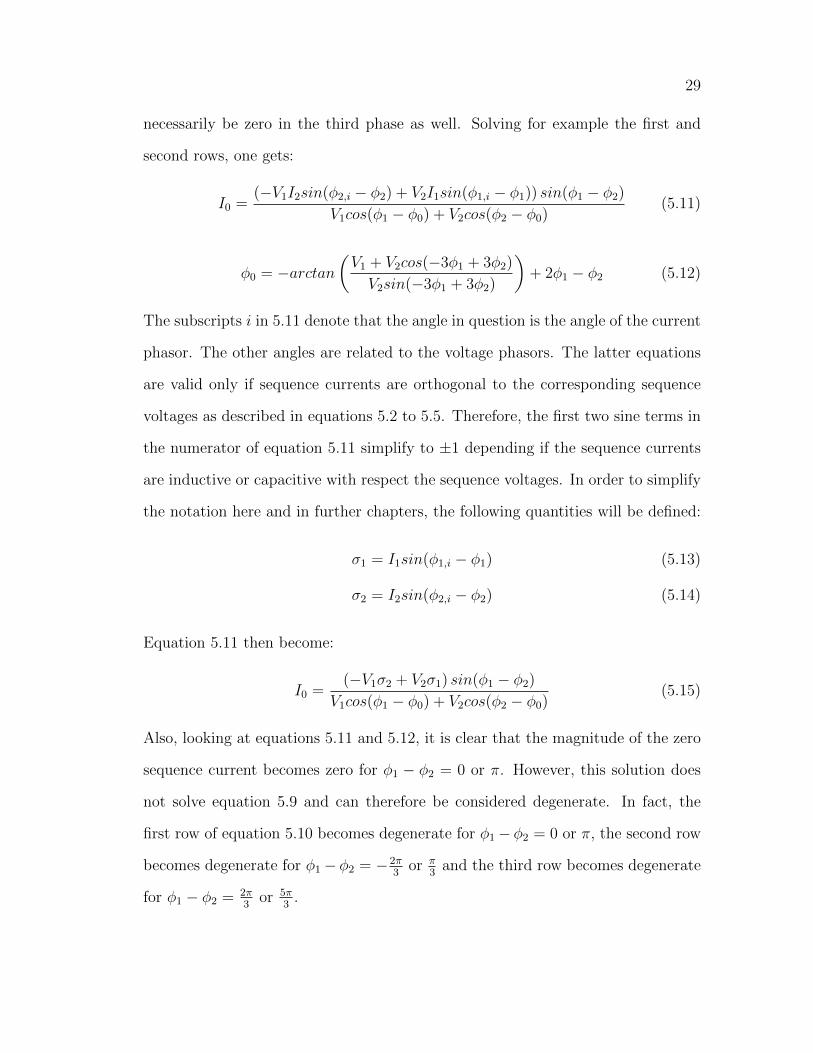
and the common mode reactive powers in positive and negative sequence are chosen
as:
Q11 = −0.1924 (8.27)
Q22 = 0.0962 (8.28)
The angle between the positive sequence and negative sequence voltages is then
varied from 0°to 360°by steps of 1°. At every step, the optimization algorithm is
run to compute the optimal leg currents. The figure below shows in blue the mag-
nitude of the current in the leg having the highest current when the optimization
method is not used. In other words, for the blue curve, equations 8.11 and 8.12 are
enforced, leaving no degree of freedom for the optimization of leg currents. The
Angle Difference (degrees)
Maxim
um
Leg
Current(pu)
0.0
0.2
0.4
0.6
0.8
1.0
1.2
0 50 100 150 200 250 300 350
Figure 8–1: Optimization of leg currents using common mode active power flow
green curve is the magnitude of the current in the leg having the highest current

46
when the optimization method is used. In other words, for the green curve, equa-
tion 8.14 was used instead of equations 8.11 and 8.12, leaving a degree of freedom
for the optimization of leg currents. The largest difference between the two curves
is approximately 7%. Although this is a relatively small difference, this optimiza-
tion method is a low cost improvement since it does not require any additional
components. Indeed, only software changes are required in order to apply this
method.
CHAPTER 9Unbalance Between Cells in a Given Phase
One additional type of unbalance is that which occurs between cells of the
same phase. Indeed, even though commom mode and differential mode active
power flow can be controlled using the methods explained in the previous chapters,
there may still be a drift in cell voltages within a given phase of the converter.
This phenomenon may have many causes, some of which are
• Slightly different component values in different cells
• Slightly different losses in different cells
• Small errors in switching time of the IGBTs
In order to correct this drift, it is necessary to exchange energy between cells of
the same phase. Selective swapping algorithms such as the one described in [12]
and [11] exist in order to re-order the switching patterns of the cell and therefore
adjust the time during which each individual cell is charged/discharged. An al-
ternative method is presented in chapter 12 of this thesis, and its effectiveness is
demonstrated in chapter 13. The advantage of this method is that it can be im-
plemented in simple logic implemented outside the main controller and therefore
does not require centralized control of all cells. This is done by measuring the
DC voltage of each cell, and adding to the AC voltage reference for the SPWM of
each cell a small voltage component which is in phase with the leg current based
on whether the capacitor should be charged or discharged. In fact, this method
amounts to creating a small active power flow in/out of the cells that need charg-
ing/discharging. Since this is done for all cells at the same time, the situation for
the whole leg amounts to an exchange of energy between the cells. The problem
47
48
with this method is that it requires a current to flow in the leg. Indeed, it is im-
possible to exchange energy without having current flow. This means that when
the STATCOM is at zero reactive power output, there cannot be an exchange of
energy between the cells. However, for the delta-coupled STATCOM or for the
wye-coupled STATCOM with neutral current path, even when the net reactive
power output of the STATCOM is zero, it is possible to circulate a third harmonic
zero sequence current. This third harmonic will not create an active power flow
in/out of the phases because the product of a fundamental frequency voltage with
a third harmonic current is zero on average. However, if the AC voltage reference
of the cells that need charging/discharging is modified to include a small third
harmonic voltage in phase with the leg current, active power will flow in/out of the
cells with the third harmonic current.

CHAPTER 10Double Wye-Coupled Chain-Link STATCOM with Half-Bridge Cells
The double-wye coupled STATCOM topology presented in this chapter relies
on the use of half-bridge cells rather than full-bridge cells as for the topologies
presented in the previous chapters. Since a half-bridge can only have 2 switching
states, its output voltage can only be 0 or VDC . For this reason, two converters are
necessary in order to operate over the full range of the ac voltage waveform. A dou-
ble wye coupled chain-link STATCOM with half-bridge cells is shown in figure 10–1.
The upper and lower converters have leg voltages with identical AC components,
and DC components of equal magnitude but opposite polarity. The upper and
lower converters also supply identical AC currents. The major advantage of the
double-wye STATCOM resides in the fact that the flow of active power created by
unbalanced operation can be cancelled with DC currents. Indeed, expressing the
voltages of the upper and lower converter legs:
~VU = ~V1
1
a2
a
+ ~V2
1
a
a2
+VDC
2
1
1
1
(10.1)
~VL = ~V1
1
a2
a
+ ~V2
1
a
a2
− VDC2
1
1
1
(10.2)
49
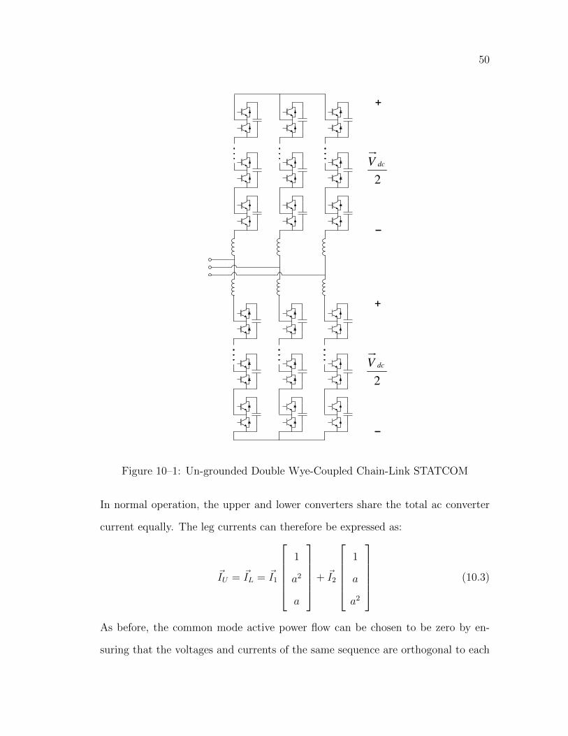
50
2
dcV
2
dcV
Figure 10–1: Un-grounded Double Wye-Coupled Chain-Link STATCOM
In normal operation, the upper and lower converters share the total ac converter
current equally. The leg currents can therefore be expressed as:
~IU = ~IL = ~I1
1
a2
a
+ ~I2
1
a
a2
(10.3)
As before, the common mode active power flow can be chosen to be zero by en-
suring that the voltages and currents of the same sequence are orthogonal to each

51
other. The unbalanced active power in the upper and lower converters can then be
calculated as follows:
~PU = Re
~V1~I∗2
1
a
a2
+ ~V2~I∗1
1
a2
a
+VDC
2~I∗1
1
a
a2
+VDC
2~I∗2
1
a2
a
(10.4)
~PL = Re
~V1~I∗2
1
a
a2
+ ~V2~I∗1
1
a2
a
− VDC2~I∗1
1
a
a2
− VDC2~I∗2
1
a2
a
(10.5)
Note that the three rows of 10.4 and 10.5 represent the sums of the terms resulting
in unbalanced active power flow in each of the three phases. The product of DC
voltages with AC currents give an average value of zero. In other words, they
represent pulsating power and do not contribute to the net active power flow in
or out of the legs. Therefore, the only terms contributing to a net flow of active
power are the same for the upper and lower converters and are:
~PU = ~PL = Re
~V1~I∗2
1
a
a2
+ ~V2~I∗1
1
a2
a
(10.6)
The idea is then to choose a DC current that will give a product with the DC
voltage that couteracts the active power flow caused by the unbalanced operating
conditions. Since the DC voltages of the upper and lower converters are of the
same magnitude but of opposite polarity, and since the unbalanced active power
flows are equal, a DC current of same amplitude but of opposite polarity is needed

52
in the upper and lower converter legs of the same phase in order to correct the
situation. Also, because these DC currents are used only to correct the differential
active power flow terms, the sum of the DC currents in all three phases needs to be
zero. These two conditions ensure that no DC current flows out of the converter
and into the grid. The DC currents in the upper converter are therefore defined
by setting the following equality:
VDC2
IDC,a
IDC,b
IDC,c
= −Re
~V1~I∗2
1
a
a2
+ ~V2~I∗1
1
a2
a
(10.7)
and the DC currents are simplyIDC,a
IDC,b
IDC,c
= − 2
VDCRe
~V1~I∗2
1
a
a2
+ ~V2~I∗1
1
a2
a
(10.8)
As described previously, the DC currents in the lower converter are then the neg-
ative of the currents defined in equation 10.8 for the corresponding phases.
This method has the major advantage that the balancing is done solely by
DC quantities without interfering with the AC quantities. It is however possible
to combine the DC current method described above with one or more of the zero
sequence methods defined in the previous chapters in order to reduce leg voltages
and currents. Indeed, in a manner similar to the one presented in chapter 7, the zero
sequence voltage method can be applied to both the upper and lower converters
up to the point where the leg voltage rating is met. The remaining differential
active power flow can then be cancelled by using the DC current method. The
first step for this method is to calculate the zero sequence voltage that would be
necessary to cancel the differential active power flow if only this method was used.

53
The individual AC phase to neutral voltages (where the neutral is the neutral point
of each wye-coupled STATCOM) can then be written as:
~Va = 1V0e(φ0)+ 1V1e
(φ1) + 1V2e(φ2) (10.9)
~Vb = 1V0e(φ0)+a2V1e
(φ1)+ aV2e(φ2) (10.10)
~Vc = 1V0e(φ0)+ aV1e
(φ1) +a2V2e(φ2) (10.11)
The inequality condition is then solved for each phase. For example, the inequality
condition for phase a is:
‖~Va‖ = ‖V0e(φ0) + V1e(φ1) + V2e
(φ2)‖ ≤ Vmax (10.12)
Solving for the amplitude of ~V0:
V0 ≤ − (V1cos(φ0 − φ1) + V2cos(φ0 − φ2))
±√
(V1cos(φ0 − φ1) + V2cos(φ0 − φ2))2 − (V 2
1 + V 22 + 2V1V2cos(φ1 − φ2)− V 2
max)
(10.13)
Negative solutions for V0 are then discarded since the angle of ~V0 has already been
defined. The smallest solution from all three phases is taken as the largest allowed
V0. Finally, the remaining unbalance is cancelled by the DC current method which
gives the following currents in the upper converter:IDC,a
IDC,b
IDC,c
=−2
VDCRe
~V1~I∗2
1
a
a2
+ ~V2~I∗1
1
a2
a
+ ~V0~I∗1
1
a
a2
+ ~V0~I∗2
1
a2
a
(10.14)
54
The DC currents found with equation 10.14 are necessarily lower or equal to the DC
currents that would be needed if that method was used without the zero sequence
voltage method.
If the converter has a neutral path, the zero sequence current method can also
be used in a similar way. Indeed, the zero sequence current method can be used to
the extent where the leg currents reach a defined limit. The remaining differential
active power flow is then cancelled using the DC current method. First, the zero
sequence current is computed as if only that method was used. The individual AC
phase currents are then:
~Ia = 1I0e(φ0)+ 1I1e
(φ1) + 1I2e(φ2) (10.15)
~Ib = 1I0e(φ0)+a2I1e
(φ1)+ aI2e(φ2) (10.16)
~Ic = 1I0e(φ0)+ aI1e
(φ1) +a2I2e(φ2) (10.17)
The inequality condition is then solved for each phase. For example, the inequality
condition for phase a is:
‖~Ia‖ = ‖I0e(φ0) + I1e(φ1) + I2e
(φ2)‖ ≤ Imax (10.18)
Solving for the amplitude of ~I0:
I0 ≤ − (I1cos(φ0 − φ1) + I2cos(φ0 − φ2))
±√
(I1cos(φ0 − φ1) + I2cos(φ0 − φ2))2 − (I21 + I22 + 2I1I2cos(φ1 − φ2)− I2max)
(10.19)
Negative solutions for I0 are discarded since the angle of ~I0 has already been defined.
The smallest solution from all three phases is taken as the largest allowed I0.
Finally, the remaining unbalance is cancelled by the DC current method which
55
gives the following currents in the upper converter:IDC,a
IDC,b
IDC,c
=−2
VDCRe
~V1~I∗2
1
a
a2
+ ~V2~I∗1
1
a2
a
+ ~V1~I∗0
1
a2
a
+ ~V2~I∗0
1
a
a2
(10.20)
The DC currents found with equation 10.20 are necessarily lower or equal to the DC
currents that would be needed if that method was used without the zero sequence
current method. As discussed in chapter 7, the neutral path impedance has in fact
a non-zero impedance. This results in the fact that a zero sequence current would
create a zero sequence voltage drop along the neutral path. The methods defined in
chapter 7 for a STATCOM with a fixed or variable neutral path impedance should
therefore be used. In that case, the leg voltage limits and the leg current limits
should then be checked simultaneously in order to find the necessary DC currents.
It must be noted that if the purpose of using the zero sequence current method
is to reduce the necessary DC current, little gain is made since this hardly reduces
the total necessary leg current. One use of this method can however be to reduce
the leg voltage. Indeed, assuming one of the legs has a high voltage due to the
unbalanced network voltages, the zero-sequence current can be used to generate
a zero sequence voltage which reduces the total voltage in that particular phase.
This will most likely result in a larger differential active power flow, which can
however still be cancelled by the DC current method. The zero sequence voltage
method can also be directly used in this way.
CHAPTER 11Comparison of Chain-Link STATCOM Topologies
The delta coupled STATCOM presented in chapter 5, the ungrounded wye-
coupled STATCOM presented in chapter 6, the grounded wye-coupled STATCOM
presented in chapter 7 and the double-wye STATCOM with or without neutral path
presented in chapter 10 can be compared based on operating range, complexity and
cost in order to define the strengths and weaknesses of each one. The comparison
of operating ranges is done using phasor diagrams. These diagrams show phase
voltages and STATCOM currents during certain faults and STATCOM operating
conditions. The intent is to show the limitations of different STATCOM topologies
by illustrating that for certain faults and operating conditions, a given STATCOM
topology may not be able to produce the required zero sequence voltage or zero
sequence current necessary to keep the DC capacitor voltages balanced. It will be
shown that these limitations are different for each STATCOM topology, and occur
during different operating conditions. The faults discussed here are explained in
appendix C, and are summarized in table C–1. In order to facilitate the reader’s
understanding of the phasor diagrams presented in this chapter, the following con-
vention will be used. This convention is also illustrated in figure 11–1.
The phase voltages and leg currents are thick vectors, and the current phasors
are a darker shade of the same color as the phase voltages. The thinner dashed
vectors of a given color are the positive and negative sequence components of the
phase quantity of the same color. The thick black vector is the zero sequence
component of either phase voltages or leg currents depending on which converter
topology (and therefore which control method) is used in the case which is shown in
56

57
Phase voltage Va
+ and - seq. components of Va
Phase voltage Vb
+ and - seq. components of Vb
Phase voltage Vc
+ and - seq. components of Vc
Leg current Ia
+ and - seq. components of Ia
Leg current Ib
+ and - seq. components of Ib
Leg current Ic
+ and - seq. components of Ic
Zero seq. components ofphase voltages or leg currents
Figure 11–1: Legend for interpreting phasor diagrams
the phasor diagram. Note that the positive, negative and zero sequence components
are added vectorially to construct the phase quantities.
11.1 Delta-Coupled STATCOM
It must be noted that for the delta-coupled converter, it may not be possible for
the STATCOM to supply both the desired common mode positive sequence reactive
power and the desired common mode negative sequence reactive power during
certain unbalanced conditions while simultaneously controlling the DC capacitor
voltages. For example, referring to table C–1, if the positive sequence voltage and
the negative sequence voltage have the same amplitude as is the case for a phase
to phase fault, a zero sequence current with an infinite magnitude is necessary
to ensure that no unbalanced active power flows. As derived in appendix C and
summarized in table C–1, the symmetrical components of the network voltage

58
during a bolted phase to phase fault at the STATCOM busbar between phases b
and c are:
~V0 = 0.5V 6 0 (11.1)
~V1 = 0.5V 6 0 (11.2)
~V2 = 0 (11.3)
where V is the positive sequence voltage of the healthy network. Figure 11–2 shows
Real
Imaginary
−1.5
−1.0
−0.5
0.0
0.5
1.0
1.5
−1.5 −1.0 −0.5 0.0 0.5 1.0 1.5
Va
Vb
Vc
Ia
Ib
Ic
I0
Figure 11–2: Phase Voltages and Positive Sequence Leg Currents in a Delta-Coupled STATCOM During a Phase to Phase Fault
the voltages appearing across the STATCOM legs as well as, for example, a positive
sequence capacitive leg current of 0.5 6 0 which the STATCOM could be required
to supply during the fault. It is clear from this figure that unbalanced active
power will flow since not all three currents are in quadrature with their respective

59
Real
Imaginary
−1.5
−1.0
−0.5
0.0
0.5
1.0
1.5
−1.5 −1.0 −0.5 0.0 0.5 1.0 1.5
Va
Vb
Vc
Ia
Ib
Ic
I0
Figure 11–3: Phase Voltages and Positive Sequence Leg Currents in a Delta-Coupled STATCOM During a Phase to Phase Fault with Zero Sequence CurrentInjection
voltages. Trying to balance the active power flow only by using a zero sequence
current results in the need for an infinite zero sequence current. This is illustrated
in figure 11–3 where a 1pu component of zero sequence current is shown in black.
Although it helps in balancing the active power flow, it is clearly insufficient. Since
preventing an unbalance in DC capacitor voltages is essential, another constraint
needs to be relaxed because it is obvious that such a large zero sequence current
cannot be allowed to flow.
It is interesting to note that the ungrounded wye-coupled STATCOM could
cope with this situation. Indeed, as shown in figure 11–4, a finite zero sequence volt-
age can be found which ensures that the leg currents and voltages are in quadrature
with each other thus cancelling all active power flow. Also, from a cost perspec-

60
Real
Imaginary
−1.5
−1.0
−0.5
0.0
0.5
1.0
1.5
−1.5 −1.0 −0.5 0.0 0.5 1.0 1.5
Va
Vb
Vc
Ia
Ib
Ic
V0
Figure 11–4: Phase Voltages and Positive Sequence Leg Currents in a Wye-CoupledSTATCOM During a Phase to Phase Fault with Zero Sequence Voltage Injection
tive, the leg voltages are a factor√
3 higher than for the wye coupled converter,
therefore more series connected cells are needed.
11.2 Ungrounded Wye-Coupled STATCOM
In the same manner, the wye-coupled converter also has certain limitations.
Stating the problem differently, it may not be possible for the STATCOM to supply
both the desired common mode positive sequence currents and the desired com-
mon mode negative sequence currents during certain unbalanced conditions while
simultaneously controlling the DC capacitor voltages. For example, if the positive
sequence current and the negative sequence current have the same amplitude and
phase, a zero sequence voltage with an infinite magnitude is necessary to ensure
that no unbalanced active power flows. To illustrate this example, the STATCOM

61
could be required to supply the following currents
~I1 = 0.5 6π
2(11.4)
~I2 = 0.5 6π
2(11.5)
while the positive sequence network voltage is 1V 6 0. This case does not correspond
to a specific fault case but could occur if, for example, the STATCOM was used
to compensate for an unbalanced load. Figure 11–5 shows the voltages appearing
across the STATCOM legs as well as a leg currents which the STATCOM should
supply in this case.The current phasors are a darker shade of the same color as the
Real
Imaginary
−1.5
−1.0
−0.5
0.0
0.5
1.0
1.5
−1.5 −1.0 −0.5 0.0 0.5 1.0 1.5
Va
Vb
Vc
Ia
Ib
Ic
V0
Figure 11–5: Positive Sequence Phase Voltages and Unbalanced Leg Currents in aWye-Coupled STATCOM
phase voltages. It is clear from this figure that unbalanced active power will flow
since not all three currents are in quadrature with their respective voltages. Trying
to balance the active power flow only by using a zero sequence voltage results in

62
the need for an infinite zero sequence voltage. This is illustrated in figure 11–6
where a 1pu component of zero sequence voltage is shown in black. Although it
helps in balancing the active power flow, it is clearly insufficient. Since preventing
Real
Imaginary
−1.5
−1.0
−0.5
0.0
0.5
1.0
1.5
−1.5 −1.0 −0.5 0.0 0.5 1.0 1.5
Va
Vb
Vc
Ia
Ib
Ic
V0
Figure 11–6: Positive Sequence Phase Voltages and Unbalanced Leg Currents in aWye-Coupled STATCOM with Zero Sequence Voltage Injection
an unbalance in DC capacitor voltages is essential, another constraint needs to
be relaxed because it is obvious that such a large zero sequence current cannot
be allowed to flow. It is interesting to note that the delta-coupled STATCOM
could cope with this situation. Indeed, as shown in figure 11–7, a finite zero
sequence current can be found which ensures that the leg currents and voltages are
in quadrature with each other thus cancelling all active power flow. Also, from a
cost perspective, the leg currents are a factor√
3 higher than for the delta coupled
converter, therefore more parallel connected cells are needed.

63
Real
Imaginary
−1.5
−1.0
−0.5
0.0
0.5
1.0
1.5
−1.5 −1.0 −0.5 0.0 0.5 1.0 1.5
Va
Vb
Vc
Ia
Ib
Ic
I0
Figure 11–7: Positive Sequence Phase Voltages and Unbalanced Leg Currents in aDelta-Coupled STATCOM with Zero Sequence Current Injection
11.3 Grounded Wye-Coupled STATCOM
As described in chapter 7 the grounded wye-coupled STATCOM has a non-
zero neutral path impedance, and therefore, both the zero sequence current and the
zero sequence voltage methods can be used to balance the differential mode active
power flow. If a fixed impedance is used, its value must be chosen carefully in order
to coordinate with the desired contributions of each zero sequence quantities. If a
variable impedance is used, the neutral path impedance can vary from an open-
circuit where the zero sequence voltage method can be utilized alone, to a low
impedance grounding path where mainly the zero sequence current method can be
utilized. In this case, the STATCOM becomes more flexible in the sense that it can
cope with both of the situations presented sections 11.1 and 11.2. This additional
flexibility however comes at the cost of a variable impedance in the neutral path.

64
11.4 Double Wye-Coupled STATCOM
The double wye-coupled STATCOM has as much flexibility as the grounded
wye coupled STATCOM with a variable neutral path impedance since there always
exist finite DC currents which will cancel the differential mode active power flow.
Furthermore, the zero sequence methods can also be used to optimize the leg
currents and voltages. The cost of this converter is slightly higher than the cost
for a same size single wye-coupled converter. Indeed, the number of semiconductor
devices in this topology is the same as for a single wye-coupled due to the fact
that half-bridge cells are used instead of full H-bridge cells. The number of DC
capacitors is doubled, but the size of each capacitor is half of the capacitors in the
single wye-coupled converter for a given STATCOM size.
11.5 Summary of STATCOM Topology Comparison
The following table summarizes the comparison of STATCOM topologies de-
scribed in this chapter.
Table 11–1: Summary of STATCOM topology comparison
Topology Operating Range Complexity Cost
Delta Limited when ~V1 and ~V2 Low High due to rating
are in phase and of equal for ph-ph voltage
amplitude
Ungrounded Limited when ~I1 and ~I2 Low Low due to rating
Wye are in phase and of equal for ph-g voltage
amplitude
Grounded Not limited by specific High due to var- High due to var-
Wye operating conditions iable impedance iable impedance
Double Not limited by specific High due to Low (assuming a
Wye operating conditions double wye large STATCOM)

CHAPTER 12Implementation of Control Strategies in Matlab/Simulink
A simple STATCOM model was implemented in Matlab/Simulink for each of
the topologies presented in order to test the control strategies that were developed.
Due to the fact that the modeling is very similar for all topologies, only the wye-
coupled STATCOM is shown in details.
12.1 Converter Modeling
The test circuit used is shown in figure 12–1. The network model is a simple
anetU ,
bnetU ,
cnetU ,
anetZ
,
bnetZ
,
cnetZ
,
1,adcU
+
−
2,adcU
+
−
3,adcU
+
−
1,bdcU
+
−
2,bdcU
+
−
3,bdcU
+
−
1,cdcU
+
−
2,cdcU
+
−
3,cdcU
+
−
aacI ,
bacI ,
cacI ,
Figure 12–1: Test circuit used in Matlab/Simulink simulations
grounded network with an R-L Thevenin impedance. The load is resistive, and
enables dynamic changes in active power absorption as well as unbalance. Finally,
the STATCOM is wye-coupled with a floating neutral. It has three cells per phase
which is sufficient to demonstrate the efficiency of the DC capacitor unbalance
correction. In order to accelerate simulation time, and to avoid complicating the
model unnecessarily, each converter cell is replaced by a controllable voltage source
as shown in figure 12–2. This simplification is acceptable because the purpose is
65

66
anetU ,
bnetU ,
cnetU ,
anetZ
,
bnetZ
,
cnetZ
,
aacI ,
bacI ,
cacI ,
1,aacU 2,aacU 3,aacU
1,bacU 2,bacU 3,bacU
1,cacU 2,cacU 3,cacU
+ − + − + −
+ − + − + −
+ − + − + −
Figure 12–2: Simplified test circuit used in Matlab/Simulink simulations
not to model the actual switching of the cells, but rather to test the DC capacitor
voltage balancing algorithms. Of course, in order to do this, the dynamics of the DC
capacitors must be modeled. Figure 12–3 shows how this is achieved. Figures 12–3a
−+ac
U
refU
acI
refI
dcI
−+dc
U
dcI
acI
acU
dcU
÷
×C
1
dcU
)a )b
)c
s
1
Figure 12–3: Modeling of converter cells as controllable voltage sources
and 12–3b show the AC and DC dynamics respectively. The voltages and currents
from each of these circuits are related according to equation 12.1.
Idc =Iac · UacUdc
(12.1)

67
This is essentially saying that there is conservation of power between the AC side
and the DC side of the cell. Furthermore, a capacitor has a transfer function of
the form:
v(s)
i(s)= z(s) =
1
sC(12.2)
Equations 12.1 and 12.2 are then implemented as shown in figure 12–3c. A more
elaborate model of the cell also includes losses. These can be modeled by using
a resistor Rp in parallel with the ideal capacitor, and a series resistor Rs. In this
case, the transfer function becomes:
v(s)
i(s)= z(s) =
Rp
sCRp + 1+Rs (12.3)
The behaviour of such a cell model is close to the behaviour of a cell model with
switching elements. The main difference is that the high order harmonics caused
by the PWM are not modeled. This has little impact on the behaviour of the DC
voltage balancing algorithms, and the simplification is therefore acceptable. For a
real converter cell, the reference voltage computed by the controller would normally
be used in the PWM process as described in chapter 3. In the case of the simplified
cell models described above, the reference is directly applied as the input to the
controllable voltage source.
12.2 STATCOM Controls
The positive sequence voltage control loop described in figure 2–3 is imple-
mented, and a negative sequence voltage control loop is added. This results in the
controls presented in figure 12–4. The inputs from the various DC voltage con-
trollers are also shown in figure 12–4. Each of these controllers will be presented
in the following sections.

68
���
��
���
���
�����
���
�������
��������
�������
���
��
���
��
��
��
��
��
�� �
���
��
���
��
��
��
��
��
��
�������
�� ������
���
��
!�"�� �
!�"�� �
!�"�� �
!#���$�%"��
�#���$�%
&��'#���$'��
���
��
���
���
�����
���
(�������
��������
�������
���
��
���
��
��
��
��
��
�� �
���
��
���
��
��
��
��
��
��
�������
�� ������
��� �
��
)
!#���$%"*���+
!�"�� �
!�"�� �
!�"�� �
!#���$� "��
,
�#���$�
)
2φ
��� �
)
))
!��
- ��*%�����%���������%���+%.�%
�������%�������%��% ��+%��/01
))
)
��
��
- ��*%����������%
�������%���%.�%�������%
����������%��% ��+%��/21
- ��*%!/�����%�������%
���%.�%�������%
����������%��% ��+%��/31
4���
��������
�������
�
4���
��������
�������
�
����%.�%
�������%
����������
- ��+%��/51
�� �������% ��%
����������%�����
!#���$%"*���+
����%.�%
��������
Figure 12–4: Full controls of the STATCOM
12.3 DC Voltage Controls
The DC capacitor voltage balancing is then implemented in three separate
control loops. The first control loop regulates the average voltage of all cells in the
converter, the second loop regulates the average voltage of all cells in each leg, and
the third control regulates the voltage in each cell. These nested control loops are
more efficient than having only localized DC voltage correction in each cell. The
reason is that these localized methods rely on the detection of an error in DC volt-
age. The first and third control loops operate on a similar principle; acting on an
error measurement. The second control loop however, relies on measured network
voltages and STATCOM currents in order to anticipate DC voltage drift caused
by unbalanced operation. This method anticipates the error and take corrective
measures in order to prevent it. This is therefore much faster and efficient than
methods which rely on the detection of an error.

69
12.3.1 Total Converter Average DC Voltage
The first control loop takes the sum of all DC voltages and controls it to a
reference with the use of a proportional-integral (PI) controller. The implemen-
tation of this control loop is shown in figure 12–5. Note that the sum of all DC
voltages (Udc,conv) is computed in figure 12–7. The output of this controller is a
s
1
iK
pK
dI
convdcU
,
Figure 12–5: Control loop for total converter average DC voltage
direct component of positive sequence leg current which is added to the current
reference of the STATCOM. As described in chapter 4, the common mode flow
of active power created by the direct current component charges evenly the entire
STATCOM.
12.3.2 Converter Leg Average DC Voltage
The second control loop acts on the sum of all DC voltages in each converter
leg. It is actually implemented as two different controllers. The first one is a pre-
dictive control which implements the zero sequence method developed in chapter 6.
Figure 12–6 shows the implementation of this controller. The output of this con-
troller is a zero sequence voltage which is then added to the converter AC voltage
reference for each STATCOM leg. This reference is the one that each MMC based
converter leg will follow. The summation of the converter AC voltage reference and
the zero sequence voltage is shown as the last summation on the right of the control
diagram shown in figure 12–4. This ensures that the converter legs do not absorb
differential mode active power during unbalanced conditions. This controller acts

70
aI
,1
ai,
,1
φ
aV
,1
a,1
φ
bI
,1
bi,
,1
φ
bV
,1
b,1
φ
cI
,1
ci,
,1
φ
cV
,1
c,1
φ
a,1
σ
b,1
σ
c,1
σ
aI
,2
ai,
,2
φ
aV
,2
a,2
φ
bI
,2
bi,
,2
φ
bV
,2
b,2
φ
cI
,2
ci,
,2
φ
cV
,2
c,2
φ
a,2
σ
b,2
σ
c,2
σ
a,1
φa,
2φ
()
()
()
()
()
()
20
21
01
21
12
21
0
21
21
21
21
2
0
sin
sin
sin
23
3co
s
33
sin
arcta
n
φφ
σφ
φσ
φφ
σσ
φφ
φφ
σσ
φφ
σφ
−+
−
−+
−=
−+�� ��
�� ��
+−
+
+−
=
VV
V
()
()
()
()
()
()
20
21
01
21
12
21
0
21
21
21
21
2
0
sin
sin
sin
23
3co
s
33
sin
arcta
n
φφ
σφ
φσ
φφ
σσ
φφ
φφ
σσ
φφ
σφ
−+
−
−+
−=
−+�� ��
�� ��
+−
+
+−
=
VV
V
()
()
()
()
()
()
20
21
01
21
12
21
0
21
21
21
21
2
0
sin
sin
sin
23
3cos
33
sin
arc
tan
φφ
σφ
φσ
φφ
σσ
φφ
φφ
σσ
φφ
σφ
−+
−
−+
−=
−+�� ��
�� ��
+−
+
+−
=
VV
V
b,1
φb,
2φ
c,1
φc,
2φ
()
2,
22sin
φφ
−i
I
()
1,
11sin
φφ
−i
I
()
2,
22sin
φφ
−i
I
()
1,
11sin
φφ
−i
I
()
2,
22sin
φφ
−i
I
()
1,
11sin
φφ
−i
I
ab
V,
0
bc
V,
0
ca
V,
0
ab
,0
φ
ca
,0
φ
bc
,0
φ3
,0
,0
,0
0
ca
bc
ab
φφ
φ
φ
++
=
ca
bc
ab
VV
Vif
,0
,0
,0
==
==
3
,0
,0
,0
0
ca
bc
ab
VV
VV
++
=
ceil
ca
bc
ab
VV
VV
els
eif
≥=
=,
0,
0,
0&
ceil
ab
ca
bc
VV
VV
els
eif
≥=
=,
0,
0,
0&
ceil
bc
ab
ca
VV
VV
els
eif
≥=
=,
0,
0,
0&
2
,0
,0
0
bc
ab
VV
V+
=
2
,0
,0
0
ca
bc
VV
V+
=
2
,0
,0
0
ab
ca
VV
V+
=
0V
0φ
Figure 12–6: Predictive control loop for converter leg average DC voltage
instantaneously, but it leaves a steady-state error due to the time delay inherent to
the voltage measurement as well as the measurement error. A second controller is

71
therefore necessary in order to get rid of this error. The second controller is similar
to the one regulating the total converter average DC voltage. Indeed, it takes the
sum of all DC voltages in each leg and controls it to a reference with the use of
a PI controller. The reference is defined as the average of total leg DC voltages.
In other words, this controller can only correct unbalance between converter leg
voltages. Therefore, it is independent from the total converter average DC voltage
controller. Figure 12–7 shows the implementation. The output of this controller
3,adcU
2,adcU
1,adcU
3,bdcU
2,bdcU
1,bdcU
3,cdcU
2,cdcU
1,cdcU
�
�
s
1
iK
pK
�
�
�
�
�
3
1
��
�
�
s
1
iK
pK
�
�
s
1
iK
pK
×
0V×
×
a
a
I
I
b
b
I
I
c
c
I
I
�
alegdcU
,
blegdcU
,
clegdcU
,
convdcU
,
avglegdcU
,,
Figure 12–7: PI control loop for converter leg average DC voltage
is a zero sequence voltage which is also added to the converter voltage reference.
One may expect that having two different controllers acting on the same quantity
might have some adverse effects. It must however be noted that these two con-
trollers have different purposes and act differently. The predictive controller acts
instantaneously only when unbalanced operation of the STATCOM is causing a
flow of differential mode active power, thus preventing converter leg voltage unbal-
ance. The PI controller acts on the converter leg voltage unbalance and is oblivious
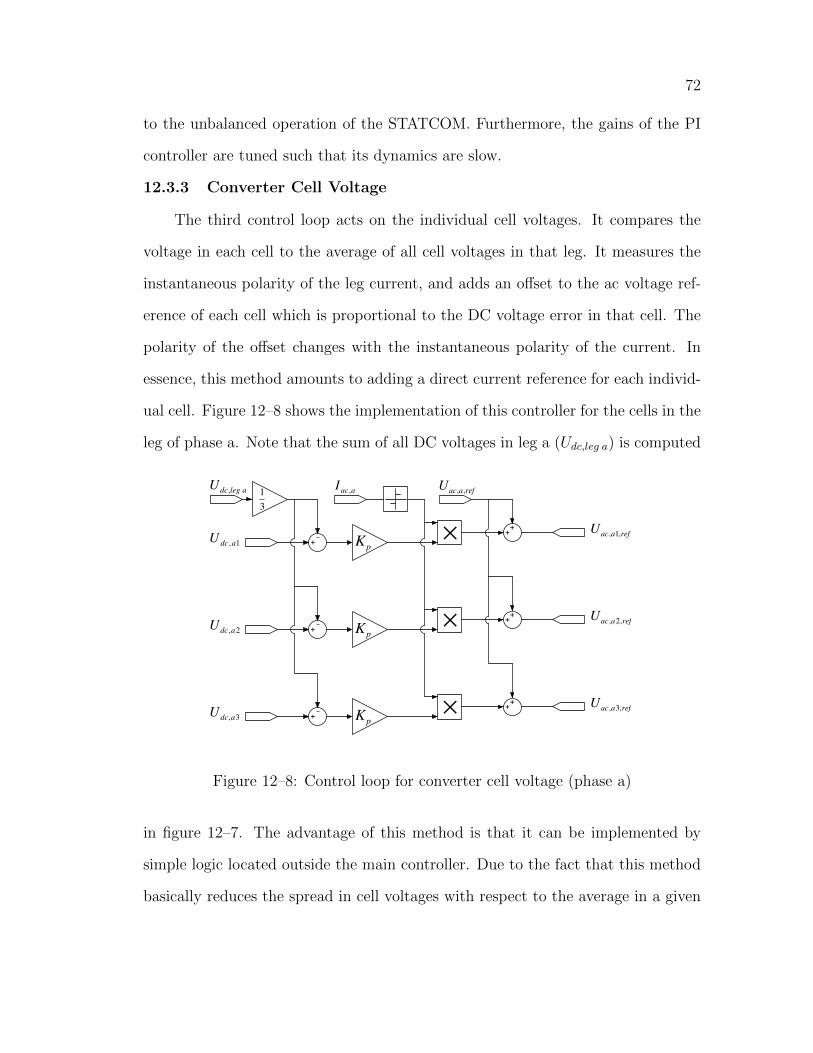
72
to the unbalanced operation of the STATCOM. Furthermore, the gains of the PI
controller are tuned such that its dynamics are slow.
12.3.3 Converter Cell Voltage
The third control loop acts on the individual cell voltages. It compares the
voltage in each cell to the average of all cell voltages in that leg. It measures the
instantaneous polarity of the leg current, and adds an offset to the ac voltage ref-
erence of each cell which is proportional to the DC voltage error in that cell. The
polarity of the offset changes with the instantaneous polarity of the current. In
essence, this method amounts to adding a direct current reference for each individ-
ual cell. Figure 12–8 shows the implementation of this controller for the cells in the
leg of phase a. Note that the sum of all DC voltages in leg a (Udc,leg a) is computed
3,adcU
2,adcU
1,adcU
pK
×
×
×
alegdcU
,
�
�
�
pK
pK
aacI
,
�
�
�
refaacU
,,
�
�
�
refaacU
,1,
refaacU
,2,
refaacU
,3,
3
1
Figure 12–8: Control loop for converter cell voltage (phase a)
in figure 12–7. The advantage of this method is that it can be implemented by
simple logic located outside the main controller. Due to the fact that this method
basically reduces the spread in cell voltages with respect to the average in a given

73
leg, it does not change this average value. This controller is therefore independent
from the two other controllers.
The efficiency of the controllers presented in this chapter was tested by simu-
lation. The controls were first tested as a whole system, and then each DC voltage
controller was tested individually. The results are presented in the next chapter.

CHAPTER 13Simulation Results
In order to demonstrate the efficiency of the DC voltage control method, dif-
ferent scenarios are simulated. The simulations presented in this chapter are done
with the wye-coupled MMC based STATCOM with floating neutral, and the con-
trols used are those developed in chapter 6 and implemented in chapter 12.
Firstly, in order to have a reference case, a fault is simulated while the STAT-
COM is not active. The AC voltage is therefore not regulated. Then, the same
fault is simulated while the STATCOM is active and regulates the AC voltage.
The DC voltage controls are however not active. This shows how the cell voltages
drift during the fault. Finally, the same fault case is simulated again. This time,
the DC voltage controls are active, and the result is that the cell voltages do not
drift during the fault.
In the last sections of this chapter, the individual control loops shown in
chapter 12 are disabled one after the other to show their effect on the cell voltages.
13.1 Phase to Phase Fault with no STATCOM
In order to have a base case to compare other simulations with, a phase to
phase fault is applied between phases B and C while the STATCOM is not in
operation. Phase to phase faults are generally less common than phase to ground
faults. Nevertheless, this type of fault was chosen because in the model described
in chapter 12, the coupling transformer was not modeled. If a WYE-delta coupling
transformer is used, a phase to ground fault on the primary of the transfomer is
seen as a phase to phase fault on the secondary. Figure 13–1 shows the sequence
voltages across the STATCOM legs resulting from this simulation.
74

75
Time (s)
Voltage
sequen
cecompon
ents
(pu)
0.0
0.2
0.4
0.6
0.8
1.0
1.2
1.4
1.5 2.0 2.5 3.0
Pos. sequenceNeg. sequenceZero sequence
Figure 13–1: Sequence voltages (STATCOM inactive)
Time (s)
Phasevoltages
(pu)
−2.0
−1.0
0.0
1.0
2.0
1.90 1.95 2.00 2.05 2.10 2.15 2.20
Time (s)
Leg
currents
(pu)
−2.0
−1.0
0.0
1.0
2.0
1.90 1.95 2.00 2.05 2.10 2.15 2.20
Figure 13–2: Phase voltages and currents (STATCOM inactive)

76
Before the fault is applied, the load is balanced, and results in a positive
sequence voltage at the point of common coupling of 0.97 pu. At t = 2s, a high
impedance phase to phase fault is applied for a duration of 250 ms. During the
fault, the positive sequence voltage drops to 0.83 pu, and a negative sequence
voltage of 0.24 pu appears. The phase to ground voltages and STATCOM currents
are shown in figure 13–2. The effect of the fault is seen on the voltages, while the
STATCOM leg currents are of course zero since the STATCOM is not active during
this simulation.
13.2 Phase to Phase Fault with STATCOM (no DC voltage control)
The same fault case is then repeated with the STATCOM connected, but with
the DC voltage controls disabled. Figure 13–3 shows the sequence voltages across
the STATCOM legs resulting from this simulation. This time, the STATCOM
Time (s)
Voltage
sequen
cecompon
ents
(pu)
0.0
0.2
0.4
0.6
0.8
1.0
1.2
1.4
1.5 2.0 2.5 3.0
Pos. sequenceNeg. sequenceZero sequence
Figure 13–3: Sequence voltages (STATCOM active but no DC voltage control)
controls the positive sequence voltage to a reference of 1.0 pu before the fault.

77
At t = 2s, a high impedance phase to phase fault is applied for a duration of
250 ms. During the fault, the STATCOM reacts to support the positive sequence
voltage, while the negative sequence voltage control is inactive in order to simplify
the simulations. As can be seen in figure 13–3, the positive sequence voltage only
drops to 0.91 pu this time, while the negative sequence voltage remains relatively
unchanged. The phase to ground voltages and STATCOM currents are shown in
figure 13–4.
Time (s)
Phasevoltages
(pu)
−2.0
−1.0
0.0
1.0
2.0
1.90 1.95 2.00 2.05 2.10 2.15 2.20
Time (s)
Leg
currents
(pu)
−2.0
−1.0
0.0
1.0
2.0
1.90 1.95 2.00 2.05 2.10 2.15 2.20
Figure 13–4: Phase voltages and currents (STATCOM active but no DC voltagecontrol)
The DC capacitor voltages are shown in figure 13–5. Each of the three sub-
plots shows the cell DC voltages of all three cells in blue while the reference is
shown in red. It is clear from this figure that the cell DC voltages drift during the
fault. The drift stops when the fault is cleared, and the voltage unbalance disap-
pears. The drift is of course unacceptable and illustrates the necessity for the DC

78
voltage control scheme developed in chapter 6 and implemented in chapter 12. The
following section will show the results of the same fault, but with the DC voltage
controls of the STATCOM enabled.
Time (s)Cellvolt.A
(pu)
0.20
0.40
0.60
1.5 2.0 2.5 3.0
Time (s)Cellvolt.B
(pu)
0.20
0.40
0.60
1.5 2.0 2.5 3.0
Time (s)Cellvolt.C
(pu)
0.20
0.40
0.60
1.5 2.0 2.5 3.0
Figure 13–5: Cell voltages (STATCOM active but no DC voltage control)
13.3 Phase to Phase Fault with STATCOM (with DC voltage control)
In order to prevent the drift in DC voltage seen in the previous section, the
DC voltage controls implemented in chapter 12 are enabled. The same fault case
is simulated, and the resulting sequence voltages across the STATCOM legs are
shown in figure 13–6. It can be seen from this figure that the positive and negative
sequence voltages are the same as in the previous simulation, but this time, a zero
sequence voltage with a magnitude of 0.25 pu also appears. This voltage is ordered
by the DC voltage control loops in order to prevent the sum of the cell voltages in
each phase to drift apart.

79
Time (s)
Voltage
sequen
cecompon
ents
(pu)
0.0
0.2
0.4
0.6
0.8
1.0
1.2
1.4
1.5 2.0 2.5 3.0
Pos. sequenceNeg. sequenceZero sequence
Figure 13–6: Sequence voltages (STATCOM active and DC voltage control en-abled)
The phase to ground voltages and STATCOM currents are shown in figure 13–
7. Comparing this figure with figure 13–4, one sees that the AC behavior of the
STATCOM is unchanged by the DC voltage control. Note that the zero sequence
voltage does not appear in the phase to ground quantities. It appears only across
the converter legs.
The individual cell DC voltages are shown in figure 13–8. It can be seen
in this figure that the DC voltage control loops are functioning correctly since
all cell voltages now closely follow the references. It is interesting to note that
a second harmonic component is present in the DC voltage. This is due to the
fact that the STATCOM is now supplying reactive power, and this results in a
charging/discharging of the DC capacitors at every half-cycle.

80
Time (s)
Phasevoltag
es(pu)
−2.0
−1.0
0.0
1.0
2.0
1.90 1.95 2.00 2.05 2.10 2.15 2.20
Time (s)
Leg
currents
(pu)
−2.0
−1.0
0.0
1.0
2.0
1.90 1.95 2.00 2.05 2.10 2.15 2.20
Figure 13–7: Phase voltages and currents (STATCOM active and DC voltage con-trol enabled)
Time (s)Cellvolt.A
(pu)
0.35
0.40
0.45
1.5 2.0 2.5 3.0
Time (s)Cellvolt.B
(pu)
0.35
0.40
0.45
1.5 2.0 2.5 3.0
Time (s)Cellvolt.C
(pu)
0.35
0.40
0.45
1.5 2.0 2.5 3.0
Figure 13–8: Cell voltages (STATCOM active and DC voltage control enabled)

81
The magnitude of the second harmonic component depends on the magnitude
of the STATCOM output, and therefore, a higher amplitude is visible during the
fault. This ripple is therefore part of the normal operation of the STATCOM, and
must be tolerated by the controls. Since the purpose of the controls developed here
is to control only the DC voltage, it suffices to filter the ripple from the capacitor
voltage measurements in order to retrieve the DC quantity which is of interest.
13.4 Test of Individual control loops
In the following subsections, all the DC control loops implemented in chap-
ter 12 are tested individually in order to show their effect on the cell DC voltages.
13.4.1 Total Converter Average DC Voltage Control Loop
In order to test that the control loop for total converter average DC voltage
of figure 12–5 is working correctly, a step is applied to its reference.
Time (s)Cellvolt.A
(pu)
0.35
0.40
0.45
1.5 2.0 2.5 3.0
Time (s)Cellvolt.B
(pu)
0.35
0.40
0.45
1.5 2.0 2.5 3.0
Time (s)Cellvolt.C
(pu)
0.35
0.40
0.45
1.5 2.0 2.5 3.0
Figure 13–9: Cell voltages after a step in total converter avg. DC voltage reference

82
Figure 13–9 shows the individual cell DC voltages. It is clear that all cell DC
voltages change. The fact that they all change together indicates that neither the
converter leg average DC voltage controller nor the converter cell voltage controller
are affected by the step change in reference for the total converter average DC
voltage controller.
13.4.2 Test of PI based Converter Leg Average DC Voltage ControlLoop
In order to show the purpose of the PI based control loop for converter leg
average DC voltage shown in figure 12–7, the same phase to phase fault as in
sections 13.1 to 13.3 is applied again, but this time, the PI controller is disabled.
The resulting cell DC voltages are shown in figure 13–10. It is clear from this
Time (s)Cellvolt.A
(pu)
0.35
0.40
0.45
1.5 2.0 2.5 3.0
Time (s)Cellvolt.B
(pu)
0.35
0.40
0.45
1.5 2.0 2.5 3.0
Time (s)Cellvolt.C
(pu)
0.35
0.40
0.45
1.5 2.0 2.5 3.0
Figure 13–10: Cell voltages (PI controller for leg avg. DC voltage disabled)
figure that the predictive control loop works correctly since the DC voltages do
not drift during the fault. However, as explained earlier, the non-ideal voltage and

83
current measurements, as well as the reaction time of the STATCOM result in a
steady-state error. By comparing figure 13–10 with figure 13–8 one immediately
sees that when the PI controller for leg average DC voltage balancing is disabled,
a steady-state error appears.
13.4.3 Test of Predictive Converter Leg Average DC Voltage ControlLoop
In order to show the purpose of the predictive control loop for converter leg
average DC voltage shown in figure 12–6, the same phase to phase fault as in
sections 13.1 to 13.3 is applied again, but this time, the predictive controller is
disabled. The resulting cell DC voltages are shown in figure 13–11. It is clear from
Time (s)Cellvolt.A
(pu)
0.35
0.40
0.45
1.5 2.0 2.5 3.0
Time (s)Cellvolt.B
(pu)
0.35
0.40
0.45
1.5 2.0 2.5 3.0
Time (s)Cellvolt.C
(pu)
0.35
0.40
0.45
1.5 2.0 2.5 3.0
Figure 13–11: Cell voltages (Predictive leg avg. DC voltage controller disabled)
this figure that the PI based control loop works correctly since the error in the
DC voltages tends to zero after some time. However, by comparing figure 13–11
with figure 13–8 one immediately sees that response of the controls is slower and a
84
larger drift in DC voltage occurs. This is because the predictive controller is faster
that the PI based controller by nature.
The case where both leg average DC voltage controllers are disabled has al-
ready been shown in figure 13–5. It is obvious from that figure that the leg average
DC voltage controllers are necessary because without them, the leg DC voltages
drift considerably.
13.4.4 Test of Converter Cell Voltage Control Loop
In order to show that the control loop for converter cell voltage of figure 12–
8 is working correctly, a small workaround is necessary. Indeed, the attentive
reader will have noticed that in all figures showing the cell DC voltages so far,
only one waveform appears in the plot of each phase. However, each of these plots
should actually show three waveforms: one for each of the cells of each phase.
The reason why only one waveform appears is that actually all three waveforms
follow each other exactly. This is due to the fact that the cells are modeled using
the simplification described in section 12–3. To show that the control loop for
converter cell voltage is working correctly, the integrators of each of the cells in
phase A are initialized to different values. The resulting cell DC voltages are shown
in figure 13–12. The three different cell voltages can now be seen in the plot of
phase A. The figure also shows how the control loop for cell voltage of each cell
corrects the error between the cell voltage and the reference, which is the average
of all three cell voltages in phase A.

85
Time (s)Cellvolt.A
(pu)
0.35
0.40
0.45
1.5 2.0 2.5 3.0
Time (s)Cellvolt.B
(pu)
0.35
0.40
0.45
1.5 2.0 2.5 3.0
Time (s)Cellvolt.C
(pu)
0.35
0.40
0.45
1.5 2.0 2.5 3.0
Figure 13–12: Unbalanced cell voltages within the same phase (phase A)
13.5 Summary
In this chapter, it was demonstrated in sections 13.1 to 13.3 that the DC volt-
age controls developed in this thesis for the the wye-coupled STATCOM function
correctly globally. Furthermore, section 13.4 demonstrated that each of the control
loops has its purpose and is necessary in order to correctly control the cell DC
voltages.
The controls developed in chapters 5 and 7 respectively for the delta-coupled
converter and wye-coupled converter with neutral path are similar in implemen-
tation to what has been shown in chapter 12 for the wye-coupled converter with
floating neutral. The validations results are also similar to those presented in this
chapter.
CHAPTER 14Conclusion
The problem of DC capacitor voltage balancing in MMC based STATCOMs
during unbalanced operating conditions was defined in chapter 4. It was explained
that a change in DC voltage of the capacitors occurs if they are subject to a net
flow of active power.
The active power flowing into the STATCOM was expressed in terms of prod-
ucts of sequence voltages and sequence currents, and it was shown that these terms
can be grouped in two categories: those creating common mode active power flow,
and those creating differential mode active power flow. The flow of common mode
active power is caused by the products of voltages and currents of the same se-
quence, and is easily controlled to zero by ensuring that the STATCOM leg voltages
and currents of same sequence are in quadrature. The flow of differential mode ac-
tive power is caused by the product of voltages and currents of different sequences,
and the method for controlling differential mode active power flow depends on the
STATCOM topology.
Subsequent chapters then presented various STATCOM topologies, and a so-
lution for controlling the flow of differential mode active power was developed for
each topology. Chapter 5 presented a delta-coupled STATCOM, and it was shown
that by imposing a zero-sequence current to flow inside the delta connection, the
differential mode active power flow can be cancelled. Chapter 6 presented a wye-
coupled STATCOM with ungrounded neutral, and it was shown that by imposing
a zero-sequence voltage on the neutral point, the differential mode active power
86

87
flow can be cancelled. Chapter 7 presented a wye-coupled STATCOM with a neu-
tral path, and it was shown that a combination of zero-sequence voltage and zero
sequence current can be used to cancel the differential mode active power flow.
Finally, chapter 10 presented a double wye-coupled STATCOM, and it was shown
that in addition to the zero sequence current and zero sequence voltage methods
developed in the previous chapters, a DC current can also be used to exchange
active power between the corresponding legs of both wye-coupled STATCOMs. It
was explained how these methods can be used individually or combined together
in order to cancel the differential mode active power flow.
The implementation in Matlab/Simulink of a wye-coupled MMC based STAT-
COM with ungrounded neutral as well as the required DC voltage controls were
presented in chapter 12. The validation of these controls was then done by simu-
lation, and the results were presented in chapter 13. The proposed controls were
shown to function adequately, and the main objective of this thesis was therefore
achieved.
The converter topologies presented in this report were also compared, and were
shown to each have their advantages and drawbacks from a performance and cost
point of view. The optimal topology for a given application greatly depends on the
required voltage level and desired reactive power output, as well as the unbalance
conditions in which the STATCOM will be operating.
The single-wye with floating neutral and the delta-coupled STATCOMs are
cost effective solutions due to the fact that they require a minimum of compo-
nents. However, their operating ranges are greatly reduced during unbalanced
operation, and required overrating of the voltage capability in the case of the wye-
coupled STATCOM and overrating of the current capability in the case of the delta
coupled STATCOM. An alternative to this is the wye-coupled STATCOM with

88
grounded neutral, where the neutral path is equipped with a variable impedance.
This topology has the major advantage that in unbalanced operating conditions,
any combination of the zero sequence voltage and the zero sequence method can be
used. This results in a larger operating range, and a converter which has a lower
current and voltage rating.
The double wye-coupled STATCOM topology with floating neutrals does how-
ever stand out as being the most flexible from the point of view of its operating
range. It is also similar in terms of cost to a single wye-coupled STATCOM of sim-
ilar size. Its main drawbacks are its increased size, and the fact that this solution
is only economical if the required STATCOM size is large enough to be able to be
split into two smaller wye converters.
It would therefore be interesting to perform a cost/benefit analysis of the
wye-coupled STATCOM with a variable impedance in the neutral path to verify if
the additional flexibiliy provided by this solution is worth the investment for the
additional components which are required.
It would also be interesting to investigate the feasibility of implementing the
optimization method described in chapter 8 in real-time. The available computa-
tion power is limited by the hardware platform used to implement the control and
protection software functions of the STATCOM, and it may therefore be a chal-
lenge to implement in real-time such computation-intensive nonlinear optimization
methods.

CHAPTER 15Future Work
As possible future work, it would be interesting to perform a cost/benefit
analysis of the wye-coupled STATCOM with a variable impedance in the neutral
path to verify if the additional flexibiliy provided by this solution is worth the
investment for the additional components which are required.
It would also be interesting to investigate the feasibility of implementing the
optimization method described in chapter 8 in real-time. The available computa-
tion power is limited by the hardware platform used to implement the control and
protection software functions of the STATCOM, and it may therefore be a chal-
lenge to implement in real-time such computation-intensive nonlinear optimization
methods.
The implementation of the voltage and current limitations of the various
topologies, as well as the dynamic behaviour of the STATCOM when these limits
are reached during transient conditions is also a topic where further investigations
are needed.
Finally, the effect of sampling and measurement delays should be investigated
in order assess the performance and stability of the proposed control methods for
DC voltage balancing.
89

References
[1] G.P. Adam, S. Finney, B. Williams, D. Trainer, C. Oates, and D. Critchley.Network Fault Tolerant Voltage-Source-Converters for High-Voltage Applica-tions. 9th IET International Conference on AC and DC Power Transmission,pages 54–54, 2010.
[2] A. Antonopoulos, L. Angquist, and H. Nee. On Dynamics and Voltage Controlof the Modular Multilevel Converter. 13th European Conference on PowerElectronics and Applications, 2009.
[3] R.E. Betz, G. Mirzaeva, C. Townsend, and T. Summers. Feed-forward Com-pensation for Multilevel Cascaded H-bridge StatComs. 13th European Con-ference on Power Electronics and Applications, 2009.
[4] R.E. Betz, T. Summers, and T. Furney. Symmetry Compensation using H-Bridge Multilevel STATCOM with Zero Sequence Injection. 41st IEEE In-dustry Applications Conference Annual Meeting, pages 1724–1731, 2006.
[5] R.E. Betz, T. Summers, and G. Mirzaeva. Dead-time Compensation for Mul-tilevel Cascaded H-bridge Converter with Novel Voltage Balancing. 13th Eu-ropean Conference on Power Electronics and Applications, 2009.
[6] M. Bollen and I. Gu. On the Analysis of Voltage and Current Transientsin Three-Phase Power Systems. IEEE Transactions on Power Delivery,vol. 22(no. 2):1194–1201, April 2007.
[7] S. Boyd and L. Vandenberghe. Convex Optimization. Cambridge UniversityPress, 2004.
[8] A. Consoli, G. Oriti, A. Testa, and A. Julian. Induction motor modeling forcommon mode and differential mode emission evaluation. 31st IEEE IndustryApplications Conference, vol. 1:595–599, October 1996.
[9] J. Dorn, M. Pohl, D. Retzmann, and F. Schettler. Transformation of theEnergy System in Germany - Enhancement of System Stability by integrationof innovative Multilevel HVDC in the AC Grid. IEEE International ETG-Congress 2013, November 2013.
[10] J. D. Glover, M. S. Sarma, and T. J. Overbye. Power System Analysis andDesign (Fourth Edition). Cengage Learning, 2008.
90

91
[11] B. Gultekin, C. Gercek, T. Atalik, M. Deniz, N. Bicer, M. Ermis, K. Kose,C. Ermis, E. Koc, I. Cadirci, A. Acik, Y. Akkaya, H. Toygar, and S. Bideci.Design and implementation of a 154-kV +- 50-Mvar Transmission STATCOMBased on 21-Level Cascaded Multilevel Converter. IEEE Transactions onIndustry Applications, vol. 48(no. 3):1030–1045, June 2012.
[12] B. Gultekin, C. Gercek, T. Atalik, M. Deniz, N. Bicer, M. Ermis, K. Kose,C. Ermis, E. Koc, I. Cadirci, A. Acik, Y. Akkaya, H. Toygar, and S. Bideci.Cascaded Multilevel Converter-Based Transmission STATCOM: System De-sign Methodology and Development of a 12kV +- 12 MVAr Power Stage. IEEETransactions on Power Electronics, vol. 28(no. 11):4930–4950, November 2013.
[13] M. Hagiwara, R. Maeda, and H. Akagi. Theoretical Analysis and Controlof the Modular Multilevel Cascade Converte Based on Double-Star Chopper-Cells (MMCC-DSCC). 2010 IEEE International Power Electronics Confer-ence, pages 2029–2036, 2010.
[14] N. Hatano and T. Ise. Control Scheme of Cascaded H-Bridge STATCOM UsingZero-Sequence Voltage and Negative-Sequence Current. IEEE Transactions onPower Delivery, vol. 25(no. 2):543–550, April 2010.
[15] N. G. Hingorani and L. Gyugyi. Understanding FACTS. IEEE Press, 2000.
[16] P. Kundur. Power System Stability and Control. McGraw-Hill, 1994.
[17] A. Rasic. Performance Analysis of the Voltage Source Converter based Back-to-back Systems in Medium-voltage Networks. PhD thesis, Faculty of Engi-neering Sciences of the University of Erlangen-Nurnberg, 2009.
[18] S. Sirisukprasert, A. Huang, and J. Lai. Modeling, Analysis and Control ofCascaded-Multilevel Converter-Based STATCOM. Power Engineering SocietyGeneral Meeting, vol. 4:2561–2568, July 2003.
[19] Q. Song and W. Liu. Control of a Cascade STATCOM With Star Configura-tion Under Unbalanced Conditions. IEEE Transactions on Power Electronics,vol. 24(no. 1):45–58, January 2009.
[20] T. Summers, R. Betz, and G. Mirzaeva. Phase Leg Voltage Balancing of a Cas-caded H-Bridge Converter Based STATCOM Using Zero Sequence Injection.13th European Conference on Power Electronics and Applications, 2009.
[21] L. Tolbert, J. Chiasson, and F. Peng. Modulation Index Regulation of aMultilevel Inverter for Static Var Compensation. Power Engineering SocietyGeneral Meeting, vol. 1:194–199, July 2003.

92
[22] L. Tolbert, F. Peng, and T. Habetler. Multilevel Converters for Large ElectricDrives. IEEE Transactions on Insdustry Applications, vol. 35(no. 1):36–44,January 1999.
[23] F. Della Torre, S. Leva, and A. Morando. A Physical Decomposition of Three-Phase Variables into Common and Differential Mode Quantities. 18th Inter-national Zurich Symposium on Electromagnetic Compatibility, pages 127–130,2007.
[24] S. Vazquez, J. Leon, J. Carrasco, L. Franquelo, E. Galvan, M. Reyes,J. Sanchez, and E. Dominguez. Analysis of the Power Balance in the Cells ofa Multilevel Cascaded H-Bridge Converter. IEEE Transactions on IndustrialElectronics, vol. 57(no. 7):2287–2296, July 2010.
[25] J.H. Vivas, G. Bergna, and M. Boyra. Comparison of Multilevel Converter-Based STATCOMs. 14th European Conference on Power Electronics and Ap-plications, 2011.

APPENDIX ASymmetrical Components
The concept of symmetrical components being central to this thesis, a brief
review of the matter is presented here. It was shown by Charles L. Fortescue that
a group of n coplanar unbalanced phasors of the same nature can be represented
as the sum of n balanced systems of n phasors. An example is given in figure A–1
for three phasors representing the voltages of a three-phase electrical system.
d)b) c)
a)
Figure A–1: a: Unbalanced voltages, b: Positive seq. , c: Negative seq. , d: Zeroseq.
The three unbalanced voltages of figure A–1 a) can indeed be decomposed into the
three balanced systems of three phasors shown in figure A–1 b), c) and d).
93
94
The system in b) consists of three phasors of equal amplitude and phase shifted
by 120°. These phasors rotate anti-clockwise in the complex plane at an angular
frequency of ω and cross any given axis in an a-b-c sequence. This system is called
the positive sequence. Mathematically, we can formulate the three voltages of this
positive sequence system as:
~Va1 = V1 6 (φ1) (A.1)
~Vb1 = V1 6 (φ1 − 2π3
) (A.2)
~Vc1 = V1 6 (φ1 − 4π3
) (A.3)
The system in c) also consists of three phasors of equal amplitude and phase shifted
by 120°. These phasors rotate anticlockwise in the complex plane at an angular
frequency of ω and cross any given axis in a c-b-a sequence. This system is therefore
called the negative sequence. Mathematically, we can formulate the three voltages
of this negative sequence system as:
~Va2 = V2 6 (φ2) (A.4)
~Vb2 = V2 6 (φ2 − 4π3
) (A.5)
~Vc2 = V2 6 (φ2 − 2π3
) (A.6)
The system in d) consists of three phasors of equal amplitude and identical phase.
These phasors rotate anti-clockwise in the complex plane at an angular frequency
of ω and cross any given axis at the same time. This system is therefore called
the zero sequence. Mathematically, we can formulate the three voltages of this

95
negative sequence system as:
~Va0 = V0 6 φ0 (A.7)
~Vb0 = V0 6 φ0 (A.8)
~Vc0 = V0 6 φ0 (A.9)
To simplify the notation, it is possible to introduce an operator which represents
a rotation of 120° in the complex plane.
a = 16 2π3
(A.10)
By squaring this operator, we get:
a2 = 16 2π3· 16 2π
3= 16 4π
3(A.11)
which represents a rotation of 240° in the complex plane. It is then possible to
re-write equations (A.1) to (A.6) using (A.10) and (A.11) as follows:
~Va1 = V1 6 φ1 (A.12)
~Vb1 = a2 · V1 6 φ1 (A.13)
~Vc1 = a · V1 6 φ1 (A.14)
~Va2 = V2 6 φ2 (A.15)
~Vb2 = a · V2 6 φ2 (A.16)
~Vc2 = a2 · V2 6 φ2 (A.17)

96
To reconstruct the unbalanced phase voltages, the individual sequence components
must be added as follows:
~Va = ~Va1 + ~Va2 + ~Va0 = V1 6 φ1 + V2 6 φ2+V0 6 φ0 (A.18)
~Vb = ~Vb1 + ~Vb2 + ~Vb0 = a2 · V1 6 φ1 + a · V2 6 φ2+V0 6 φ0 (A.19)
~Vc = ~Vc1 + ~Vc2 + ~Vc0 = a · V1 6 φ1 + a2 · V2 6 φ2+V0 6 φ0 (A.20)
Equations (A.18), (A.19) and (A.20) can then be re-written in matrix form:~Va
~Vb
~Vc
=
1 1 1
1 a2 a
1 a a2
~V0
~V1
~V2
(A.21)
Finally, the inverse transformation can be found to be:~V0
~V1
~V2
=1
3
1 1 1
1 a a2
1 a2 a
~Va
~Vb
~Vc
(A.22)

APPENDIX BDifferential Mode and Common Mode Extraction for Scalar Quantities
The purpose of this appendix is to explain how to extract the differential
mode and common mode of three-phase scalar quantities. First, the concept of
differential mode and common mode quantities is defined using two variables in
order to simplify the explanation.
Taking two scalar variables x1 and x2, the common mode and the differential
mode of these variables are then:
xcomm =x1 + x2
2(B.1)
xdiff =x1 − x2
2(B.2)
Note that these equations are commonly used in signal processing, and are ap-
plicable for AC quantities as well as DC quantities. This therefore justifies their
validity for use with scalar quantities. The latter equations can then be put into
matrix form as follows: xcomm
xdiff
=1
2
1 1
1 −1
x1
x2
(B.3)
The inverse of this relationship is:
x1 = xcomm + xdiff (B.4)
x2 = xcomm − xdiff (B.5)
97

98
and in matrix form: x1
x2
=
1 1
1 −1
xcomm
xdiff
(B.6)
Another way of formulating this relationship is:
x1,diff = x1 − xcomm (B.7)
x2,diff = x2 − xcomm (B.8)
However, by definition,
x1,diff = −x2,diff = xdiff (B.9)
This means that only one of the two equations B.7 and B.8 is sufficient in order
to define xdiff if an expression for xcomm is known. Taking equation B.7, and
substituting the definition for xcomm, one gets:
x1,diff = xdiff = x1 − xcomm = x1 −x1 + x2
2=x1 − x2
2(B.10)
The latter is, as expected, the same as B.2. All the manipulations above may seem
trivial, however, the methodology developed for the case with two variables was
meant to be a simple example. The same methodology will now be used for the
case with three variables. Taking three scalar variables x1, x2 and x3, the common
mode and the differential mode of these variables are then:
xcomm =x1 + x2 + x3
3(B.11)
x1,diff = x1 − xcomm (B.12)
x2,diff = x2 − xcomm (B.13)
x3,diff = x3 − xcomm (B.14)

99
This time, by definition,
x3,diff = −x1,diff − x2,diff (B.15)
Therefore, two of the three equations B.12, B.13 and B.14 are sufficient in order
to define the differential components if an expression for xcomm is known. Taking
equations B.12 and B.13, and substituting the definition for xcomm, one gets:
x1,diff = x1 − xcomm = x1 −x1 + x2 + x3
3=
2x1 − x2 − x33
(B.16)
x2,diff = x2 − xcomm = x2 −x1 + x2 + x3
3=−x1 + 2x2 − x3
3(B.17)
Finally, putting equations B.11, B.16 and B.17 in matrix form:x1,diff
x2,diff
xcomm
=1
3
2 −1 −1
−1 2 −1
1 1 1
x1
x2
x3
(B.18)
Equation B.18 is the same as equation 2 in [23]. For reference purposes, the inverse
is: x1
x2
x3
=
1 0 1
0 1 1
−1 −1 1
x1,diff
x2,diff
xcomm
(B.19)

APPENDIX CNetwork Unbalances
C.1 Network Unbalances During Faults
This appendix gives a brief description of the behavior of network voltages
during faults. For the analysis here, it is assumed that all faults occur on the
STATCOM busbar. This assumption is justified in the sense that a bolted fault
at the terminals of the STATCOM constitues the worst possible fault condition
in terms of voltage unbalance. A fault elsewhere in the network will result in
lesser constraints on the STATCOM operating modes. For this analysis, a simple
Thevenin network equivalent is considered. That is, the network is modeled as an
ideal voltage source behind an impedance. Therefore, this model does not represent
changes in frequency or voltage angle during the fault. It is also assumed for this
analysis that the ideal three-phase source supplies only positive sequence voltages.
This appendix contains several phasor plots. The legend to interpret these plots is
given in figure 11–1.
C.1.1 Grounded Network
The first type of three-phase network model to be considered is the grounded
network as shown in figure C–1. During normal conditions, the phase voltages with
respect to ground at the point of common coupling are:
~Va = V 6 0 (C.1)
~Vb = V 6 −2π3
(C.2)
~Vc = V 6 −4π3
(C.3)
100

101
aV
bV
cV
Figure C–1: Grounded Net
Single-Phase to Ground Fault
If any of the three phases is grounded, the voltage with respect to ground for
that phase becomes zero. For example, grounding the phase a, we get:
~Va = 0 (C.4)
~Vb = V 6 −2π3
(C.5)
~Vc = V 6 −4π3
(C.6)
and by applying (A.22) we get:
~V0 = 13V 6 π (C.7)
~V1 = 23V 6 0 (C.8)
~V2 = 13V 6 π (C.9)
Figure C–2 is a phasor diagram representing the phase to ground voltages during
the fault. The symmetrical components composing each phase voltage are repre-
sented by the smaller dashed phasors.

102
Real
Imaginary
−1.5
−1.0
−0.5
0.0
0.5
1.0
1.5
−1.5 −1.0 −0.5 0.0 0.5 1.0 1.5
Va
Vb
Vc
Figure C–2: Phase voltages during a single phase to ground fault in phase a
Two-Phases to Ground Fault
If any two of the three phases are grounded, the voltages with respect to
ground for those phases become zero. For example, grounding the phases a and b,
we get:
~Va = 0 (C.10)
~Vb = 0 (C.11)
~Vc = V 6 −4π3
(C.12)

103
and by applying (A.22) we get:
~V0 = 13V 6 −4π
3(C.13)
~V1 = 13V 6 0 (C.14)
~V2 = 13V 6 −2π
3(C.15)
Figure C–3 is a phasor diagram representing the phase to ground voltages during
the fault. The symmetrical components composing each phase voltage are repre-
sented by the smaller dashed phasors.
Real
Imaginary
−1.5
−1.0
−0.5
0.0
0.5
1.0
1.5
−1.5 −1.0 −0.5 0.0 0.5 1.0 1.5
Va
Vb
Vc
Figure C–3: Phase voltages during a two phase to ground fault in phases a and b
Phase to Phase Fault
If two phases are connected together but not to ground, the voltage with
respect to ground for these two phases will of course be the same. For example,
figure C–4 shows the case where phases b and c are connected together. To calculate

104
aV
bV
cV x
V
I
Figure C–4: Phase to Phase fault in a grounded network
the voltage which appears at the connection point of the faulted phases, KVL is
first applied around the loop.
~Vb − ~I ~Zl = ~Vc + ~I ~Zl (C.16)
~I ~Zl =~Vb − ~Vc
2(C.17)
Then, solving for ~Vx we get:
~Vx = ~Vb − ~I ~Zl (C.18)
=~Vb + ~Vc
2(C.19)
Since the ideal three-phase source supplies positive sequence voltages only, the
latter expression can be simplified as:
~Vx = 12V 6 π (C.20)

105
The voltages during the fault are therefore:
~Va = V 6 0 (C.21)
~Vb = 12V 6 π (C.22)
~Vc = 12V 6 π (C.23)
and by applying (A.22) we get:
~V0 = 0 (C.24)
~V1 = 12V 6 0 (C.25)
~V2 = 12V 6 0 (C.26)
Figure C–5 is a phasor diagram representing the phase to ground voltages during
the fault. The symmetrical components composing each phase voltage are repre-
Real
Imag
inary
−1.5
−1.0
−0.5
0.0
0.5
1.0
1.5
−1.5 −1.0 −0.5 0.0 0.5 1.0 1.5
Va
Vb
Vc
Figure C–5: Phase voltages during a phase to phase fault between phases b and c

106
sented by the smaller dashed phasors.
Three-Phase Fault
The three-phase fault is a balanced fault and therefore creates no unbalances
in the voltages. The fact that the fault is three-phase to ground or simply three-
phase makes no difference here because it is assumed that the sources provide only
positive sequence voltage, and the series impedances are equal. Therefore, in the
event of a three-phase fault, the voltages become:
~Va = 0 (C.27)
~Vb = 0 (C.28)
~Vc = 0 (C.29)
and of course, by applying (A.22) we simply get:
~V0 = 0 (C.30)
~V1 = 0 (C.31)
~V2 = 0 (C.32)
C.1.2 Ungrounded Network
The second type of three-phase network model to be considered is the un-
grounded network as shown in figure C–6. During normal conditions, the phase
voltages with respect to ground at the point of common coupling are indentical to
the previous model, that is:
~Va = V 6 0 (C.33)
~Vb = V 6 −2π3
(C.34)
~Vc = V 6 −4π3
(C.35)
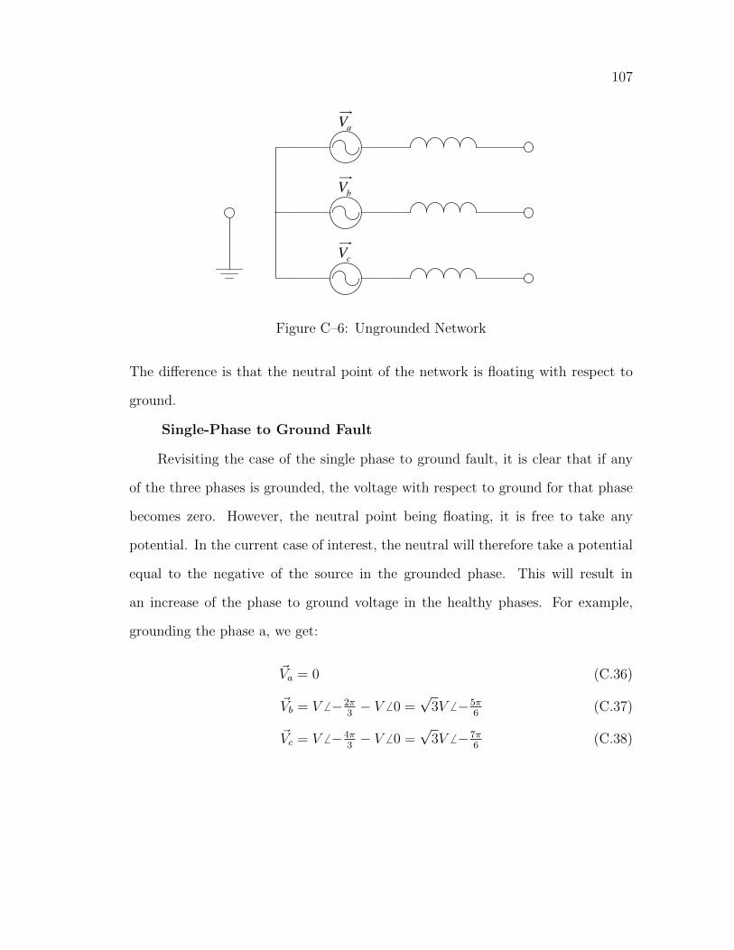
107
aV
bV
cV
Figure C–6: Ungrounded Network
The difference is that the neutral point of the network is floating with respect to
ground.
Single-Phase to Ground Fault
Revisiting the case of the single phase to ground fault, it is clear that if any
of the three phases is grounded, the voltage with respect to ground for that phase
becomes zero. However, the neutral point being floating, it is free to take any
potential. In the current case of interest, the neutral will therefore take a potential
equal to the negative of the source in the grounded phase. This will result in
an increase of the phase to ground voltage in the healthy phases. For example,
grounding the phase a, we get:
~Va = 0 (C.36)
~Vb = V 6 −2π3− V 6 0 =
√3V 6 −5π
6(C.37)
~Vc = V 6 −4π3− V 6 0 =
√3V 6 −7π
6(C.38)

108
and by applying (A.22) we get:
~V0 = V 6 π (C.39)
~V1 = V 6 0 (C.40)
~V2 = 0 (C.41)
Figure C–7 is a phasor diagram representing the phase to ground voltages during
the fault. The symmetrical components composing each phase voltage are repre-
sented by the smaller dashed phasors.
Real
Imaginary
−1.5
−1.0
−0.5
0.0
0.5
1.0
1.5
−1.5 −1.0 −0.5 0.0 0.5 1.0 1.5
Va
Vb
Vc
Figure C–7: Phase voltages during a single phase to ground fault in phase a
Two-Phases to Ground Fault
If any two of the three phases are grounded, the voltages with respect to
ground for those phases become zero. However, the neutral point being floating,
it is free to take any potential. In the current case of interest, the neutral will

109
therefore take a non-zero potential. For example, grounding the phases a and b,
we get the situation described by figure C–8 In a similar fashion to the phase to
aV
bV
cV
xV
I
Figure C–8: Two-Phase to Ground Fault in an Ungrounded Network
phase fault in the grounded network, KVL can be applied around the loop.
−~Va + ~I ~Zl = −~Vb − ~I ~Zl (C.42)
~I ~Zl =~Va − ~Vb
2(C.43)
Then, solving for ~Vx we get:
~Vx = −~Va + ~I ~Zl (C.44)
=−~Va − ~Vb
2(C.45)
Again, since the ideal three-phase source supplies positive sequence voltages only,
the latter expression can be simplified as:
~Vx = 12V 6 −4π
3(C.46)
In other words, a two-phase to ground fault in phases a and b results in an increase
of the neutral voltage by ~Vx calculated above. Therefore, the phase to ground

110
voltages at the point of common coupling become:
~Va = 0 (C.47)
~Vb = 0 (C.48)
~Vc = V 6 −4π3
+ 12V 6 −4π
3= 3
2V 6 −4π
3(C.49)
and by applying (A.22) we get:
~V0 = 12V 6 −4π
3(C.50)
~V1 = 12V 6 0 (C.51)
~V2 = 12V 6 −2π
3(C.52)
Figure C–9 is a phasor diagram representing the phase to ground voltages during
the fault. The symmetrical components composing each phase voltage are repre-
Real
Imag
inary
−1.5
−1.0
−0.5
0.0
0.5
1.0
1.5
−1.5 −1.0 −0.5 0.0 0.5 1.0 1.5
Va
Vb
Vc
Figure C–9: Phase voltages during a two phase to ground fault in phases a and b

111
sented by the smaller dashed phasors.
Phase to Phase Fault
If two phases are connected together but not to ground, the voltage with
respect to ground for these two phases will of course be the same. Revisiting
the phase to phase fault case for the grounded network but with an ungrounded
network this time, we can rewrite (C.16) and (C.17) as follows:
~Vb − ~I ~Zl + ~Vy = ~Vc + ~I ~Zl + ~Vy (C.53)
~I ~Zl =~Vb − ~Vc
2(C.54)
Where ~Vy is the voltage of the neutral point. It is clear that ~Vy has no impact on
the voltage drop across the impedance. Solving for ~Vx we get:
~Vx = ~Vy + ~Vb − ~I ~Zl (C.55)
= ~Vy +~Vb + ~Vc
2(C.56)
As shown by (C.53) and (C.54), the neutral voltage is completely independent from
the phase to phase fault condition and could take any value including zero. Since
the ideal three-phase source supplies positive sequence voltages only, and since the
impedances are balanced, it is obvious that the neutral voltage is zero prior to the
fault and therefore remains zero during the fault. The latter expression can then
be simplified as:
~Vx = 12V 6 π (C.57)

112
The voltages during the fault are therefore:
~Va = V 6 0 (C.58)
~Vb = 12V 6 π (C.59)
~Vc = 12V 6 π (C.60)
and by applying (A.22) we get:
~V0 = 0 (C.61)
~V1 = 12V 6 0 (C.62)
~V2 = 12V 6 0 (C.63)
Figure C–10 is a phasor diagram representing the phase to ground voltages during
Real
Imaginary
−1.5
−1.0
−0.5
0.0
0.5
1.0
1.5
−1.5 −1.0 −0.5 0.0 0.5 1.0 1.5
Va
Vb
Vc
Figure C–10: Phase voltages during a phase to phase fault between phases b andc

113
the fault. The symmetrical components composing each phase voltage are repre-
sented by the smaller dashed phasors.
Three-Phase Fault
The three-phase fault is a balanced fault and therefore creates no unbalances
in the voltages. Equations (C.27) to (C.32) thus remain valid.
C.2 Network Unbalances During Normal Operation
The network voltages may also be unblanced during normal operation. These
unbalances can be attributed to several phenomena occuring both at the transmis-
sion level and at the distribution level in many networks. The two main causes
of network voltage unbalances during normal operation are: unbalanced mutual
inductance between phases in a transmission line, and unbalanced loads. The fol-
lowing sections will not present an in depth analysis of these problems, but will
rather present them in a general way so that the reader may become familiar with
the concepts.
C.2.1 Transmission Line Unbalanced Impedances
A typical high voltage alternating current transmission line is shown in fig-
ure C–11. The three phase conductors are physically arranged in a coplaner man-
ner, and a neutral wire is placed above the phase conductors. The ground should
also be considered as a conductor. The voltages at the sending end and at the
receiving end of this line are:
~V s =
~V sa
~V sb
~V sc
~V se
~V sg
~V r =
~V ra
~V rb
~V rc
~V re
~V rg
(C.64)

114
a b c
g
e
Figure C–11: Typical three-phase transmission line
A primitive admittance matrix can be found which relates the currents and voltages
according to
~Ia
~Ib
~Ic
~Ie
~Ig
=
~Yaa ~Yab ~Yac ~Yae ~Yag
~Yba ~Ybb ~Ybc ~Ybe ~Ybg
~Yca ~Ycb ~Ycc ~Yce ~Ycg
~Yea ~Yeb ~Yec ~Yee ~Yeg
~Yga ~Ygb ~Ygc ~Yge ~Ygg
~V sa
~V sb
~V sc
~V se
~V sg
−
~V ra
~V rb
~V rc
~V re
~V rg
(C.65)
Since the ground conductor and the earth are at the same potential, this five
conductor system can be reduced to a three conductor equivalent by expressing the
phase voltages at both ends of the line with respect to their local ground potentials.
A full demonstration of this is presented in [10]. The result is a simplified system~Ia
~Ib
~Ic
=
~Yaaeq ~Yabeq ~Yaceq
~Ybaeq ~Ybbeq ~Ybceq
~Ycaeq ~Ycbeq ~Ycceq
(~V sa − ~V s
g
)−(~V ra − ~V r
g
)(~V sb − ~V s
g
)−(~V rb − ~V r
g
)(~V sc − ~V s
g
)−(~V rc − ~V r
g
) (C.66)

115
By transforming the simplified admittance matrix to its equivalent symmetric ad-
mittance matrix, we get
1
3
1 1 1
1 a a2
1 a2 a
~Yaaeq ~Yabeq ~Yaceq
~Ybaeq ~Ybbeq ~Ybceq
~Ycaeq ~Ycbeq ~Ycceq
1 1 1
1 a2 a
1 a a2
=
~Y00 ~Y01 ~Y02
~Y10 ~Y11 ~Y12
~Y20 ~Y21 ~Y22
(C.67)
For the latter to represent a balanced transmission line, the off-diagonal terms
must be zero. This can be understood as the requirement that a zero sequence
voltage give rise solely to a zero sequence current, a positive sequence voltage
give rise solely to a positive sequence current and a negative sequence voltage
give rise solely to a negative sequence current. In other words, a balanced line
will not create coupling between sequence networks. For the off-diagonal terms of
the symmetric admittance matrix to be zero, two constraints are imposed on the
simplified admittance matrix:
~Yaaeq = ~Ybbeq = ~Ycceq (C.68)
~Yabeq = ~Yaceq = ~Ybaeq = ~Ybceq = ~Ycaeq = ~Ycbeq (C.69)
These constraints can in turn be understood as the requirement for the self ad-
mittances of the phase conductors to be equal, and for the mutual admittances
between phases to be equal. The only way for this second requirement to be pos-
sible is for the physical arrangement of the conductors to be symmetrical with
respect to all three phase conductors. That is, the distances between phases must
be equal, the distances from each phase to the ground conductor must be equal
and the distances from each phase to the earth must be equal. The way to achieve
this in practice is to transpose the phase conductors so that over the entire length
of the transmission line, each phase conductor will be in each position equally.

116
C.2.2 Unbalanced loads
For various reasons, loads may be unbalanced as well. Often, this is caused
by the presence of single phase loads. Single phase loads are sometimes preferred
at the distribution level because they are fed by less conductors than three-phase
loads. The way to minimize this problem is to try to distribute single-phase loads
evenly on all three phases so that the total loading is approximately balanced.
C.3 Summary
The goal of this chapter was to show the worst unbalance conditions to be
expected in a network during fault conditions as well as during normal operating
conditions. The table below summarizes the results of the analysis regarding fault
conditions. With regards to transmission line and load unbalances, utilities gener-
ally try to minimize these problems by transposing long transmission lines and by
ditributing evenly unbalanced loads. The result is that network unbalances during
normal operation are usually kept at very low levels. Generally speaking, the ratio
of negative sequence voltage to positive seuquence voltage is around 1%, and the
zero sequence voltage is at negligible levels.
Table C–1 summarizes the results obtained in sections C.1.1 and C.1.2. The
reader should keep in mind that the voltage unbalances summarized in this table
were calculated using several assumptions. The major assumptions are that:
• The network model uses an ideal three-phase source which supplies only
positive sequence voltages
• The impedances are equal in all phases
• The network model is not dynamic (i.e. does not represent phase shifts or
changes in frequency during the fault)
• Transient phenomena are ignored (conditions during a fault are considered
steady-state conditions for the entire duration of the fault)

117
Table C–1: Summary of Voltage Unbalances Due to Faults
Fault Type Grounded Network Ungrounded Network
One phaseto ground
~V0 = 13V 6 π ~V0 = V 6 π
~V1 = 23V 6 0 ~V1 = V 6 0
~V2 = 13V 6 π ~V2 = 0
Two phasesto ground
~V0 = 13V 6 −4π
3~V0 = 1
2V 6 −4π
3
~V1 = 13V 6 0 ~V1 = 1
2V 6 0
~V2 = 13V 6 −2π
3~V2 = 1
2V 6 −2π
3
Phase tophase
~V0 = 0 ~V0 = 0~V1 = 1
2V 6 0 ~V1 = 1
2V 6 0
~V2 = 12V 6 0 ~V2 = 1
2V 6 0
Threephase
~V0 = 0 ~V0 = 0~V1 = 0 ~V1 = 0~V2 = 0 ~V2 = 0
Voltage unbalances may be different from those shown in table C–1 if the afore-
mentioned assumptions do not hold. However, these assumptions are justified and
sufficient for the development of the control stategies in this thesis.

APPENDIX DActive and Reactive Power Flow
The main goal of a network is of course to transmit electrical power from the
generation and to distribute it to the load centers. This appendix biefly describes
how active and reactive power flow along a transmission line. A simple two bus
network is shown in figure D–1. The direction of current flow establishes a con-
sV
rVI
LX
Figure D–1: Transmission line and active/reactive power flow
vention where the bus from which the current is originating is considered as the
sending end, while the bus to which the current is flowing is considered as the re-
ceiving end. This convention also means that generated power has a positive sign,
and absorbed power has a negative sign. For the purpose of the analysis presented
here, the line is considered as a short lossless line and is therefore modeled by a
simple reactance XL. The voltages at the sending end and receiving end are
~Vs = Vs 6 φs (D.1)
~Vr = Vr 6 φr (D.2)
The apparent power at the receiving end is therefore
Sr = ~Vr~I∗ (D.3)
118
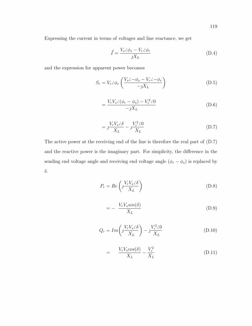
119
Expressing the current in terms of voltages and line reactance, we get
~I =Vs 6 φs − Vr 6 φr
XL
(D.4)
and the expression for apparent power becomes
Sr = Vr 6 φr
(Vs 6 −φs − Vr 6 −φr
−XL
)(D.5)
=VrVs 6 (φr − φs)− V 2
r6 0
−XL
(D.6)
= VrVs 6 δ
XL
− V2r6 0
XL
(D.7)
The active power at the receiving end of the line is therefore the real part of (D.7)
and the reactive power is the imaginary part. For simplicity, the difference in the
sending end voltage angle and receiving end voltage angle (φr − φs) is replaced by
δ.
Pr = Re
(VrVs 6 δ
XL
)(D.8)
= − VrVssin(δ)
XL
(D.9)
Qr = Im
(VrVs 6 δ
XL
)− V
2r6 0
XL
(D.10)
=VrVscos(δ)
XL
− V 2r
XL
(D.11)

120
Assuming that δ is small, (D.9) and (D.11) become
Pr ≈ −VrVsδ
XL
(D.12)
Qr ≈VrVsXL
− V 2r
XL
=Vr(Vs − Vr)
XL
(D.13)
These results show that the difference in phase angle between the sending end
voltage and the receiving end voltage has a large impact on the active power flow
on the line whereas it is the diffence in voltage magnitudes that has an impact on
the reactive power flow. The implication of this is that by controlling the reactive
power flow, the voltage magnitude at the receiving end can be controlled without
having a significant impact on the active power flow.