VLSI - 1.docx
23
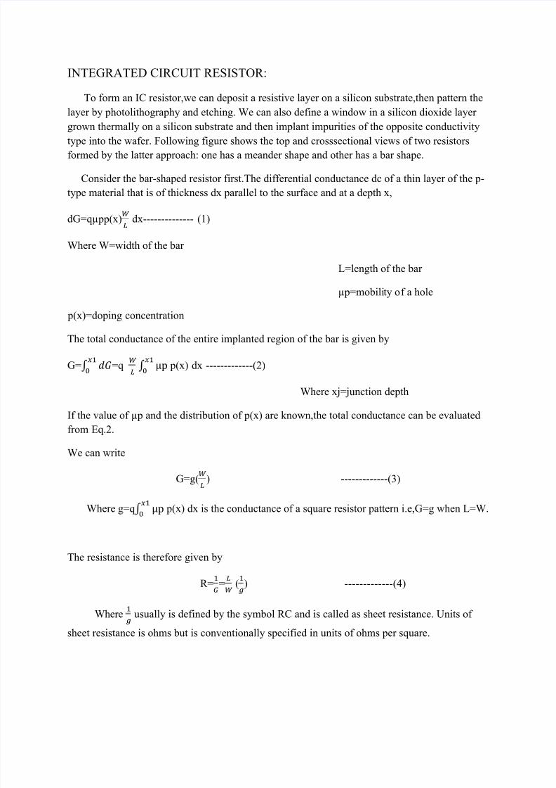
INTEGRATED CIRCUIT RESISTOR: To form an IC resistor,we can deposit a resistive layer on a silicon substrate,then pattern the layer by photolithography and etching. We can also define a window in a silicon dioxide layer grown thermally on a silicon substrate and then implant impurities of the opposite conductivity type into the wafer. Following figure shows the top and crosssectional views of two resistors formed by the latter approach: one has a meander shape and other has a bar shape. Consider the bar-shaped resistor first.The differential conductance dc of a thin layer of the p- type material that is of thickness dx parallel to the surface and at a depth x, dG=qµpp(x) dx-------------- (1) Where W=width of the bar L=length of the bar µp=mobili ty o f a hole p(x)=doping concentration The total conductance of the entire implanted region of the bar is given by G= =q p(x) dx -------------(2) Where xj=junction depth If the value of µp and the distribution of p(x) are known,the total conductance can be evaluated from Eq.2. We can write G=g( ) -------------(3) Where g=q p(x) dx is the conductance of a square resistor pattern i.e,G=g when L=W. The resistance is therefore given by R= = ( ) -------------(4) Where usually is defined by the symbol RC and is called as sheet resistance. Units of sheet resistance is ohms but is conventionally specified in units of ohms per square.
-
Upload
suda-krishnarjunarao -
Category
Documents
-
view
225 -
download
0
Transcript of VLSI - 1.docx
8/6/2019 VLSI - 1.docx
http://slidepdf.com/reader/full/vlsi-1docx 1/23
INTEGRATED CIRCUIT RESISTOR:
To form an IC resistor,we can deposit a resistive layer on a silicon substrate,then pattern thelayer by photolithography and etching. We can also define a window in a silicon dioxide layer grown thermally on a silicon substrate and then implant impurities of the opposite conductivity
type into the wafer. Following figure shows the top and crosssectional views of two resistorsformed by the latter approach: one has a meander shape and other has a bar shape.
Consider the bar-shaped resistor first.The differential conductance dc of a thin layer of the p-type material that is of thickness dx parallel to the surface and at a depth x,
dG=qµpp(x)
dx-------------- (1)
Where W=width of the bar
L=length of the bar
µp=mobility of a hole
p(x)=doping concentration
The total conductance of the entire implanted region of the bar is given by
G=
=q
�
p(x) dx -------------(2)
Where xj=junction depth
If the value of µp and the distribution of p(x) are known,the total conductance can be evaluatedfrom Eq.2.
We can write
G=g(
) -------------(3)
Where g=q �
p(x) dx is the conductance of a square resistor pattern i.e,G=g when L=W.
The resistance is therefore given by
R=
=
(
) -------------(4)
Where
usually is defined by the symbol RC and is called as sheet resistance. Units of
sheet resistance is ohms but is conventionally specified in units of ohms per square.

8/6/2019 VLSI - 1.docx
http://slidepdf.com/reader/full/vlsi-1docx 2/23
Many resistors in an IC are fabricated simultaneously by defining different geometric patterns inthe mask is shown in figure. Since the same processing cycle is used for all these resistors, it isconvenient to separate the resistance into two parts, the sheet resistance Rs, determined by the
diffusion process and the ratio of L/W is determined by the pattern lengths. Once the value of Rsis known then the ratio of L/W in the resistor pattern. The end contact areas will introduceadditional resistance to the IC resistors.
INTEGRATED CIRCUITCAPACITOR:
Basically, two types of capacitors are used in integrated circuits:MOS capacitors and p-n
junctions. The MOS capacitor can be fabricated by using a heavily doped region as one plate,thetop metal electrode as the other plate,and the intervening oxide layer as the dielectric. The topand cross-sectional views of a MOS capacitor are shown in below figure. To form a MOScapacitor, a thick oxide layer is thermally grown on a silicon substrate. Next, a window islithographically defined and etched in the oxide. Diffusion or ion implantation is used to form a p region in the windowarea,where as the surrounding thick oxide serves as a mask. A thin oxidelayer is then thermally grown in the window area, followed by a metallization step. Thacapacitance per unit area is given by
C=
------------------ (5)
Where = dielectric permittivity of SiO2
d= oxide thickness
To increase the capacitance further, insulators with higher dielectric constants are being studied,such as SiN4 and Ta2O3,which have dielectric constants of 7 and 25 respectively. The MOScapacitance is essentially independent of the applied voltage, because the lower plate of thecapacitor is made up of heavily doped material. This also reduces the associated series resistance.
A P-N junction is sometimes used as a capacitor in an integrated circuit. The top and
cross sectional views of an n-p junction capacitor as shown in below figure. As acapacitor, thedevice is usually reverse bias; i.e the P region is reverse biased w.r.t n* region. The capacitanceis not a constant, but varies as : (Vr+ Vb)-1/2
Where Vr=applied reverse voltage;
Vb=built in potential of the junction;
8/6/2019 VLSI - 1.docx
http://slidepdf.com/reader/full/vlsi-1docx 3/23
The series resistance is considerably higher than that of a MOS capacitance because the p regionhas higher resistivity than does the p* region.
PHOTOLITHOGRAPHY :
1. Photo- resist films:
Positive resist : Exposed areas are dissolved away by developing
Negative resist : Unexpected areas are dissolved away by developing
Negative resist superseded by positive resist for pattern dimensions below 3µm.This is becausenegative has poor contact characteristic and has tendency to swell.
Positive resist: It contains three components: 1.A resistor base material
2. PAC (Photo active compound)
3. Solvent
A no valance resist used for layer formation.
A photo sensitive component: Diazonaphthoquinone is most frequently used.
A solvent.
Popular positive resistors are referred to us DQN the most commonly used PAc¶s in positiveresist are the Diazonaphthoquinone (DQ) such as one is shown in figure.
The part of the molecule from so2 specific to particular manufacture and plays only a secondaryrole in the exposer process we will, therefore simplify the DQ molecule by representing it with agenetic R as shown below.
In this state , the PAC acts as an inhibitor , reducing the dissolution rate of the resist in thedeveloper by a factor of 10 or more .This occurs by a chemical bonding of the PAC and the NOVALAC at the surface of the resist when it is exposed to the envelop. For inhibitor mechanism to be operative thermal cycle such as the soft break are necessary after application.
8/6/2019 VLSI - 1.docx
http://slidepdf.com/reader/full/vlsi-1docx 4/23
The addition of UV light will free the weakly bonded nitrogen molecule from the carbon ring behind a highly reactive carbon site.
Our way to stabilize the structure is to move one of the carbons outside the ring. The oxygenatom is then covalently bonded to this external carbon atom. This is known as wolf rearrangement. The resultant molecule is called ketene. In the presence of water a finalrearrangement occurs in which double bond to the external carbon atom is replaced with a single bond and an OH group .This final product is carboxylic acid. (Dissolution enhancer)
This process acts as a PAC because the starting material will not dissolve in a base solution (one
with PH<7).carboxylic acid on the other hand, readily reacts with and dissolves in base solution.Two reasons for dissolutions:
Novalac resin itself is already water soluble and so dissolves easily.
The resin/carboxylic acid will rapidly take up water. The nitrogen released in the reaction alsoforms the resist, further assisting dissolution.
The chemical reaction that occurs during this dissolution is the breakdown of the carboxylic acidinto water soluble amines such as aniline and salts of K (or Na,depending on the developer)
This process continuous until all the exposed resist is removed .Only light, water, and theabilities to remove the nitrogen gas ate required to drift the process .Typical developer solutionsare KOH or Noah diluted with the water.
EXPOSURE: Photo resist are exposed by means of collimated UVlight a monochromatic light isrequired. During exposure with such a light source, the optical wave propagates through the
resist and is reflected backwards, resulting in a standing wave intensity pattern.
Intensity venations of this first type result in periodic changes in the development rate profit of the resist, causing striations of its side wall pattern after expose and development.
8/6/2019 VLSI - 1.docx
http://slidepdf.com/reader/full/vlsi-1docx 5/23
In addition this causes variation in the width of lines over profile surfaces.
Striation effect increases rapidly with the reflectivity of the under laying layer. They can begreatly reduced by the use of an antireflective coating (ARL).
Post bake: Biminis of this step is that it reduces striations caused by standing wave effects byredistributing photo active components which had been destroyed by optical radiation temp 100-120ºc
ION IMPLANTATION:
In this process dopand ions are implanted into the semiconductor by means of an ion beam
The doping concentration has a peak distribution inside the semiconductor.
The dopant distribution is determined mainly by the ion mass and the implanted ±ion energy.
Range of implanted ions:
Ion implantation is the introduction of energetic, charged particles into a substrate such assilicon.
Implantation energies are between 1kev and 1mev resulting in.
Ion distributions with average depths ranging from 10nm to 10µm.
Ion dose vary
From 1012 ions/cm2 for threshold voltage adjustment
To 1018 ions/cm2foe the formation of buried insulating layers.
Close is expressed as the number of ions implanted into 1cm2 of the semiconductor surface area.
Advantages:
8/6/2019 VLSI - 1.docx
http://slidepdf.com/reader/full/vlsi-1docx 6/23

8/6/2019 VLSI - 1.docx
http://slidepdf.com/reader/full/vlsi-1docx 7/23
Projected Straggle (p): The statistical fluctuations along the range are called the projectedstraggle.
Lateral Straggle (l): A statistical fluctuation along an axis perpendicular to the axis of incidence.
Diagrams
Along the axis of incidence, the implanted impurity profile can be approximated by a Gaussiandistribution function
S=ion dose per unit area
Ion Stopping: Two mechanisms.
Transferring its energy to the target nuclear: causes deflection of the incident ion and alsodislodges many target nuclei from their original lattice sites.
Nuclear stopping power Sn(E)=(dE/dX)n
E is the energy of ion at any point x along its pathBy the interaction of the ion with the cloud of electrons surrounding the target¶s atom
Electronic stopping power Se(E)=(dE/dx)e
The average rate of energy loss with distance is given by
dE/dx=Sn(E)+Se(E)
Total distance
R=�
Eo =initial ion energy
8/6/2019 VLSI - 1.docx
http://slidepdf.com/reader/full/vlsi-1docx 8/23
Idealized ion implantation systems:
Three components:
Ion source
The acceleration tube
The end station
Ion source: Starts with a feed gas
E.g. BF3, AsH3&PH3
If implant species is not available in gaseous form, a solid charge can be heated and the resultant
vapor can be used as the source. At high pressures, the electron current is often sufficient to maintain a glow discharge.
The gas flows into an arc chamber:
To break up the feed gas into a variety of atomic and molecular spices and
To ionize some of these species.
Gas flow into a low-pressure source chamber where its passes between a hot filament and ametal plate. The filament is maintained large negative potential W.R.T the plate. Electrons boil
off the filament and are accelerated towards the plate. As they do so collide with feed gasmolecules, transferring some of their energy. If the
The resulting ion beam is often a few millimeters by 1to 2cm
Gas pressure in this part of the source is 10-5to10-7 torr
Maximum ion current are typically a few mill amperes
Selection of the desired implant species is usually done with an analyzing magnet
MV2/r=qvBv =

8/6/2019 VLSI - 1.docx
http://slidepdf.com/reader/full/vlsi-1docx 9/23
Two masses and M and M+ M are said to be resolved when D is longer than the width of the beam plus the width of the exist slit.
The best resolution occurs where r is large and M is small.
Most mass filters used for fabrication have filters with a radius of a meter or less
Acceleration tube is a typically several meters long and must be maintained at a relatively highvacuum (<10-6torr)
This is necessary to avoid collisions during acceleration
The beam at this point is primarily composed of ions. Some neutrons may have reappeared.Commonly neutrons are ions that combined with thermal electrons
B11++e+ B11
They may also be ions that collided with another ion in the beam undergoing a electronexchange.
Neutrons are highly undesirable since they will not be deflected in electrostatic end stationscanning mechanism.
These neutrons will travel in a beam to wafer where they will continuously implant near thecenter of the wafer. To avoid this problem most ion implantation systems are equipped with a bend.
Ion channeling: channeling occurs when incident ions aligh with a major crytallognophicdirection and guided between rows of atoms in a crystal
8/6/2019 VLSI - 1.docx
http://slidepdf.com/reader/full/vlsi-1docx 10/23
DOPING:-
The practical use of impurity doping mainly has been to change the electrical properties of thesemiconductors.
There are two key methods of impurity doping
diffusion : is used to form a deep junction
ion implementation : is used to form a shallow junction
Formation of a dopped region by diffusion:-
Diffusion , the movement of one material through another is a natural chemical process withmany examples in every day life.
Two conditions are necessary
one of the materials must be at a higher concentration than the other
there must be sufficient energy in the system for the higher concentration materials to move in to(or) through the other
eg:-
a gas state diffusion is the action of a common pressurized spray can such as room deodorant
a liquid state diffusion is represented when a drop of ink is dropped in to a glass of water. If thewater in the glass is heated (giving the water more energy) , the ink will spread in to water faster.
solid state diffusion , when a doped water is exposed to a concentration of atoms higher than theconcentration in the wafer solid state diffusion phenomenon takes place.
Formation of junction :-
In a diffusion tube , the wafer is exported to a concentration of N-type dopants at a hightemperature . the N-type dopants diffuse through the hole in the oxide layer .
In layer no.1 the number of N-type atoms aregrater than the no. of P-type atoms converting itfrom P-type to N-type.
The diffusion process proceeds
At the second level, there are again more N-type dopants than P-type dopants , converting levelto N-type.
8/6/2019 VLSI - 1.docx
http://slidepdf.com/reader/full/vlsi-1docx 11/23
This process goes deeper in to the wafer.
The N-P junction :
At level 4 there are exactly the same number of N-type and P-type atoms .this level is thelocation of an N-P junction . The definition of an N-P junction is the location in the wafer wherethe number of N-type and P-type dopants are equal .
Below the junction , at level 5 , there are three N-type atoms , which are not enough to convertthat layer to N-type.
N-P junction indicates that there is a higher concentration of N-type dopants on one side of the jnction.
Goals of solid state diffusion :-
the creation of specific number of dopant atoms in the wafer surface.
to create the N-P (or P-N) junction at a specific distance below the wafer surface.
to create a specific distribution and concentration of dopant atoms in the wafer surface.
Lateral (or) slide ± diffusion :-
8/6/2019 VLSI - 1.docx
http://slidepdf.com/reader/full/vlsi-1docx 12/23
Some of the dopant atoms move in a lateral direction forming a junction under the oxide barrier .This is called lateral / side diffusion . The amount is approximately 85% of the vertical junctiondepth.
Concentration versus depth graphs :-
Two dimensional graphical representation of a doped region is the concentration versus depthgraphs .
The graph of an incoming dopant concentration versus depth profile for an actual , process is nota straight line . they are curved lines . The shape is determined by the physics of the dopanttechnique.
With in the wafer , the dopant atoms move by two different mechanisms :
Vacancy movement
Interstitial movement
This process is controlled or limited by several factors
Diffusivity of the particular dopant

8/6/2019 VLSI - 1.docx
http://slidepdf.com/reader/full/vlsi-1docx 13/23
Diffusivity is the rate (speed) of movement of the dopant through the particular wafer material.The higher the difficulty , the faster the dopant moves through the wafer.
Diffusivity increases with temperature.
Maximum solid solubility of the dopant in the wafer material :
It is the maximum concentration of a specific dopant that can be put in to the wafer.
Eg:- the coffee can dissolve only a certain amount of sugar before collecting in the bottom of thecup as solid.
The maximum solid solubility limit increases with increasing temperature.
Diffusion equation :-
We define a flux F as the number of dopant atoms passing through a unit area in a unit time andC as dopant concentration per unit volume.
Then we have
D-diffusivity
Note that the basic driving force of the diffusion process is the concentration gradient dc/dx
8/6/2019 VLSI - 1.docx
http://slidepdf.com/reader/full/vlsi-1docx 14/23
The flux is proportional to the concentration gradient , and the dopant atoms will move awayfrom a high concentration region toward a lower concentration region.
If F1 and F2 are not the same , the concentration of the diffusing species in the volume mustchange.
The no. of impurities in this volume element is just the product of the concentration and thedifferential volume element (A.dx).
Then the continuity equation is expressed as
From fick¶s first law this can be written
If D is assumed to be independent of position
Finally , in three dimensions for an isotropic medium , fick¶s second law is expressed as
Analysis of diffused properties :-
8/6/2019 VLSI - 1.docx
http://slidepdf.com/reader/full/vlsi-1docx 15/23
Once an impurity has diffused , it is desirable to be able to measure the impurities concentrationas a function of depth and position.
The diffusion profileof the dopant atoms is dependents on the initial and boundary conditions .
Two important cases are considered :
Constant surface concentration diffusion
Constant dopant diffusion
Constant surface concentration diffusion :-
Impurities are transported from a vapor source on to the semiconductor surface and diffused in tothe semiconductor wafer. The vapor source maintains a constant level of surface concentrationduring the entire diffusion period.
Initial condition at t=0 is c(x,0)=0
The boundary conditions are c(0,t)=Cs and c(�,t)=0
Where Cs-surface concentration (at x=0) , which is independent of time solution for fick¶s
diffusion equation that satisfies above conditions is given by
8/6/2019 VLSI - 1.docx
http://slidepdf.com/reader/full/vlsi-1docx 16/23
Total number of dopant atoms per unit area of the semi conductor is given by
Interpretation:-
The quantity Q(t) represents the area under one of the diffusion profiles of the above plot
A related quantity is the gradient of the diffusion profile dc/dx .the gradient can be obtained bydifferentiating c(x,t)
Constant total dopant diffusion :
For this case , a fixed (or constant) amount of dopant is deposited on to the semiconductor surface in a thin layer, and the dopant sequentially diffuses in to the semiconductor.
The initial condition is the same as the above C(x,0)=0
The boundary conditions are
Where S is the total amount of dopent per unit area.
The solution of the diffusion equation that satisfies the above condition is
8/6/2019 VLSI - 1.docx
http://slidepdf.com/reader/full/vlsi-1docx 17/23
This expression is the Gaussian distribution .since the dopant will move in to the semiconductor
as time increases, in order to keep the total dopent S constant ,the surface concentration mustdecrease.
This is indeed the case, since the surface concentration is given by equation (3) with x=0
Figure shows the dopent profile for a gaussiondistribution in which the normalized
concentration (c/s) is plotted as a function of the distance for three increasing diffusion lengths.
Note the reduction of the surface concentration as the diffusion time increases .
The gradient of the diffusion profile is obtained by differentiating (3) and is
The gradient (or slope ) is zero at X=0 and X=�, and the maximum gradient occurs at
8/6/2019 VLSI - 1.docx
http://slidepdf.com/reader/full/vlsi-1docx 18/23
In IC processing a two step diffusion process is commonly used , in which a pre depositiondiffused layer is first formed under the constant surface concentration condition. This step isfollowed by a drive in diffusion (also called redistribution diffusion) under a constant totaldopant condition.
For most practical cases , the diffusion length ¥DT for the pre deposition is much smaller thanthe diffusion length for the drive in diffusion . there for , the extent of the penetration of the predeposition profile can be regarded to be negligibly small compared with that of the final profilethat results from the drive-in step.
The resistance of diffused layer can be measured by a four-point probe technique shown below
The probes are equally spaced .a small current I from constant current source is passed throughthe outer probes , a voltages V is measured between inner two probes.
For a thin wafer with thickness W that is much smaller then the same diameter d, resistivity isgiven by
8/6/2019 VLSI - 1.docx
http://slidepdf.com/reader/full/vlsi-1docx 19/23
Where CF is known as the correction factor , it depends on d/s where d/s>20 the CF approaches4.54.
Diffusion systems :-
Liquid sources :-
Liquid sources of dopants an chlorinated or brominated compounds of the desired element
Boren liquid source is boron tri bromide
Phosphorous liquid source is phosphorous tri oxy chloride
Laminar flow is required to prevent gas from spiraling in the tube , creating non uniform doping.
8/6/2019 VLSI - 1.docx
http://slidepdf.com/reader/full/vlsi-1docx 20/23
A reaction gas is required to create the elemental dopant form in the tube .for BBr3 , the reactiongas is oxygen , which creates the boron oxide at the wafer surface , a boron trioxide layer deposits on the silicon , and the boron diffuses from the oxide in to the surface.
A similar reaction takes place in case of N-type dopant phosphorus also
Advantage :-
Offer the advantage of low to moderate cost and consistant doping
Disadvantages :-
Safety considerations are highly corrosive
Flasks or tubes must be pressurized and have been known to explore
Process is sensitive to small temperature changes , because the vapor pressure above the liquidincreases exponentially with temperature.
A significant danger of forming insoluble silicon components at the surface of the wafer that areinvisible , but are extremely undesirable.
The potential contamination associated with the opening of the flasks for recharging.
Gas sources :-These are hydrated forms of the dopant atom such as arsine and diborane.
8/6/2019 VLSI - 1.docx
http://slidepdf.com/reader/full/vlsi-1docx 21/23
These gases are mixed in different dilutions in the pressurized containers and connected directlyto the gas manifold.
Advantages :-
Precise control through pressure regulators
Favored for deposition on larger diameter wafers
Processes are in general chamber
Disadvantages :-
Unwanted chemical reaction in the manifold can create silica dust that can contaminate the tubeand wafers.
Solid sources :-
An oxide powder of the desired dqxent was placed on a quartz holder , called a spoon , and placed in a source furnace attached to the main deposition tube.
In the source furnace the oxide gives off source vapors that are carried in to the depositionfurnace where the diffusion takes place.
Advantage :-
Economical
Used in the doping when less precission is required
Disadvantage :-
Non uniform
Planar solid source :- solid neighbor source
8/6/2019 VLSI - 1.docx
http://slidepdf.com/reader/full/vlsi-1docx 22/23
These are wafer size slugs that contain the desired dopant boron sings are a compound of boronand nitride .slugs are also available for arsenic and phosphorus diffusions.
Advantages :-
Provides good uniformity for larger diameter wafers , since slug is the same size as the wafer
Slugs are safer to use, since no size as the wafer.
Disadvantages :-
Breakage of the slugs
Lower productivity
Necessity of cleaning.
Drive-in oxidation :-
This is the second major part of the diffusion process
Purpose :-
Redistribution of the dopant I the wafer
Growth of new oxide on the exposed silicon surface .the atmosphere in the tube is oxygen or water vapor, which performs the oxidation simultaneously as the dopants are being driven deeper in to the wafer.

8/6/2019 VLSI - 1.docx
http://slidepdf.com/reader/full/vlsi-1docx 23/23