VISVESVARAYA TECHNOLOGICAL UNIVERSITY, …vtu.ac.in/pdf/schememtech2014/vlsischsyll.pdf · 14EVE16...
55
VISVESVARAYA TECHNOLOGICAL UNIVERSITY, BELGAUM SCHEME OF TEACHING AND EXAMINATION FOR M.Tech. VLSI Design and Embedded Systems I Semester CREDIT BASED Subject Code Name of the Subject Teaching hours/week Duration of Exam in Hours Marks for Total Marks CREDITS Lecture Practical / Field Work / Assignment/ Tutorials I.A. Exam 14ELD11 Advanced Mathematics 4 2 3 50 100 150 4 14EVE12 Digital VLSI Design 4 2 3 50 100 150 4 14EVE13 Advanced Embedded Systems 4 2 3 50 100 150 4 14EVE14 VLSI Process Technology 4 2 3 50 100 150 4 14EVE15X Elective - 1 4 2 3 50 100 150 4 14EVE16 VLSI Design and Embedded System Lab -1 -- 3 3 25 50 75 2 14EVE17 Seminar on Advanced topics from refereed journals -- 3 -- 25 -- 25 1 Total 20 16 18 300 550 850 23 Elective-1: 14 ELD151 Digital System Design using Verilog 14 EVE 154 ASIC Design 14 EVE 152 VLSI Design Automation 14 EVE 155 System Verilog 14 ELD 153 Nanoelectronics
Transcript of VISVESVARAYA TECHNOLOGICAL UNIVERSITY, …vtu.ac.in/pdf/schememtech2014/vlsischsyll.pdf · 14EVE16...

VISVESVARAYA TECHNOLOGICAL UNIVERSITY, BELGAUM SCHEME OF TEACHING AND EXAMINATION FOR M.Tech. VLSI Design and Embedded Systems
I Semester CREDIT BASED
Subject Code Name of the Subject
Teaching hours/week
Duration of Exam in Hours
Marks for
Total Marks CREDITS
Lecture
Practical / Field Work / Assignment/
Tutorials
I.A. Exam
14ELD11 Advanced Mathematics 4 2 3 50 100 150 4
14EVE12 Digital VLSI Design 4 2 3 50 100 150 4
14EVE13 Advanced Embedded Systems 4 2 3 50 100 150 4
14EVE14 VLSI Process Technology 4 2 3 50 100 150 4
14EVE15X Elective - 1 4 2 3 50 100 150 4
14EVE16 VLSI Design and Embedded System Lab -1 -- 3 3 25 50 75 2
14EVE17 Seminar on Advanced topics from refereed journals
-- 3 -- 25 -- 25 1
Total 20 16 18 300 550 850 23
Elective-1:
14 ELD151 Digital System Design using Verilog 14 EVE 154 ASIC Design 14 EVE 152 VLSI Design Automation 14 EVE 155 System Verilog 14 ELD 153 Nanoelectronics

VISVESVARAYA TECHNOLOGICAL UNIVERSITY, BELGAUM SCHEME OF TEACHING AND EXAMINATION FOR M.Tech. VLSI Design and Embedded Systems
II Semester CREDIT BASED
Subject Code
Name of the Subject
Teaching hours/week
Duration of Exam in Hours
Marks for
Total Marks
CREDITS Lecture
Practical / Field Work / Assignment/
Tutorials
I.A. Exam
14EVE21 Design of Analog and Mixed mode VLSI Circuits
4 2 3 50 100 150 4
14EVE22 Low Power VLSI Design 4 2 3 50 100 150 4
14EVE23 VLSI Testing and Verification 4 2 3 50 100 150 4
14ELD 24 Real Time Operating Systems 4 2 3 50 100 150 4
14EVE25X Elective-2 4 2 3 50 100 150 4
14EVE26 VLSI Design and Embedded System Lab -2 3 3 25 50 75 2
14EVE27 Seminar on Advanced topics from refereed journals
-- 3 -- 25 -- 25 1
**Project Phase-I(6 week Duration)
Total 20 16 18 300 550 850 23
Elective-2: 14 EVE 251 VLSI for signal processing 14 EVE 254 CMOS RF Circuit Design 14 EVE 252 High Speed VLSI Design 14 EVE 255 SOC Design 14 ELD 253 MEMS
** Between the II Semester and III Semester, after availing a vocation of 2 weeks.

VISVESVARAYA TECHNOLOGICAL UNIVERSITY, BELGAUM
SCHEME OF TEACHING AND EXAMINATION FOR M.Tech. VLSI Design and Embedded Systems
III Semester: INTERNSHIP # CREDIT BASED
Course Code
Subject No. of Hrs./Week
Duration of the Exam in Hours
Marks for Total Marks
CREDITS Lecture
Practical / Field Work I.A. Exam
14EVE31 Midterm Presentation on Internship (After 8 weeks from the date of commencement) *
- - - 25 - 25 4
14EVE32 Report on Internship (After 16 weeks from the date of commencement)
- - - 75 75 12
14EVE33 Evaluation and Viva-voce - - 3 – 50 50 4
Total - - - 100 50 150 20
* The student shall make a midterm presentation of the activities undertaken during the first 8 weeks of internship to a panel comprising Internship Guide, a senior faculty from the department and Head of the Department. # The College shall facilitate and monitor the student internship program. The internship report of each student shall be submitted to the University.
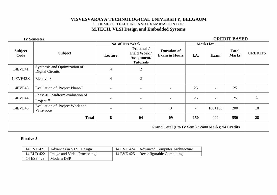
VISVESVARAYA TECHNOLOGICAL UNIVERSITY, BELGAUM SCHEME OF TEACHING AND EXAMINATION FOR
M.TECH. VLSI Design and Embedded Systems IV Semester CREDIT BASED
Subject Code Subject
No. of Hrs./Week
Duration of Exam in Hours
Marks for
Total Marks CREDITS
Lecture
Practical / Field Work / Assignment/
Tutorials
I.A. Exam
14EVE41 Synthesis and Optimization of Digital Circuits
4 2
14EVE42X Elective-3 4 2
14EVE43 Evaluation of Project Phase-I - - - 25 - 25 1
14EVE44 Phase-II : Midterm evaluation of
Project # - - - 25 - 25 1
14EVE45 Evaluation of Project Work and Viva-voce
– - 3 - 100+100 200 18
Total 8 04 09 150 400 550 28
Grand Total (I to IV Sem.) : 2400 Marks; 94 Credits
Elective-3:
14 EVE 421 Advances in VLSI Design 14 EVE 424 Advanced Computer Architecture 14 ELD 422 Image and Video Processing 14 EVE 425 Reconfigurable Computing 14 ESP 423 Modern DSP

Note:
1) Project Phase – I: 6 weeks duration shall be carried out between II and III Semesters. Candidates in consultation with the guides shall carryout literature survey / visit to Industries to finalize the topic of dissertation.
2) Project Phase – II: 16 weeks duration during III Semester. Evaluation shall be taken during the Second week of the IV Semester. Total Marks shall be 25. 3) Project Evaluation: 24 weeks duration in IV Semester. Project Work Evaluation shall be taken up at the end of the IV Semester. Project Work
Evaluation and Viva-Voce Examinations shall be conducted. Total Marks shall be 250 (Phase I Evaluation: 25 Marks, Phase –II Evaluation: 25 Marks, Project Evaluation marks by Internal Examiner (guide): 50, Project Evaluation marks by External Examiner: 50, marks for external and 100 for viva-voce).
Marks of Evaluation of Project:
• The I.A. Marks of Project Phase – I & II shall be sent to the University along with Project Work report at the end of the Semester.
4) During the final viva, students have to submit all the reports. 5) The Project Valuation and Viva-Voce will be conducted by a committee consisting of the following:
a) Head of the Department (Chairman) b) Guide c) Two Examiners appointed by the university. (Out of two external examiners at least one should be present).

Advanced Mathematics
Subject Code : 14ELD11 IA Marks : 50 No. of Lecture Hours / Week : 04 Exam. Hours : 03 Total No. of Lecture Hours : 50 Exam. Marks : 100
Matrix Theory
QR EL Decomposition – Eigen values using shifted QR algorithm- Singular Value EL Decomposition - Pseudo inverse- Least square
approximations
Calculus of Variations
Concept of Functionals- Euler’s equation – functional dependent on first and higher order derivatives – Functionals on several dependent
variables – Isoperimetric problems- Variational problems with moving boundaries
Transform Methods
Laplace transform methods for one dimensional wave equation – Displacements in a string – Longitudinal vibration of a elastic bar – Fourier
transform methods for one dimensional heat conduction problems in infinite and semi infinite rod.
Elliptic Equation
Laplace equation – Properties of harmonic functions – Fourier transform methods for laplace equations. Solution for Poisson equation by Fourier
transforms method
Linear and Non Linear Programming
Simplex Algorithm- Two Phase and Big M techniques – Duality theory- Dual Simplex method. Non Linear Programming –Constrained extremal
problems- Lagranges multiplier method- Kuhn- Tucker conditions and solutions
Reference Books:
1. Richard Bronson, "Schaum’s Outlines of Theory and Problems of Matrix Operations", McGraw-Hill, 1988.

2. Venkataraman M K, "Higher Engineering Mathematics" , National Pub. Co, 1992.
3. Elsgolts, L., "Differential Equations and Calculus of Variations" , Mir, 1977.
4. Sneddon,I.N., "Elements of Partial differential equations" , Dover Publications, 2006.
5. Sankara Rao, K., "Introduction to partial differential equations" , Prentice – Hall of India, 1995
6. Taha H A, “Operations research - An introduction" , McMilan Publishing co, 1982.

Digital VLSI Design
Subject Code : 14EVE12 IA Marks : 50 No. of Lecture Hours /week : 04 Exam Hours : 03 Total no. of Lecture Hours : 50 Exam Marks : 100
MOS Transistor: The Metal Oxide Semiconductor (MOS) Structure, The MOS System under External Bias, Structure and Operation of
MOS Transistor, MOSFET Current-Voltage Characteristics, MOSFET Scaling and Small-Geometry Effects.
MOS Inverters: Static Characteristics: Introduction, Resistive-Load Inverter, Inverters with n_Type MOSFET Load, CMOS Inverter.
MOS Inverters: Switching Characteristics and Interconnect Effects: Introduction, Delay-Time Definition, Calculation of Delay Times,
Inverter Design with Delay Constraints, Esimation of Interconnect Parasitics, Calculation of Interconnect Delay, Switching Power
Dissipation of CMOS Inverters.
Dynamic Logic Circuits : Introduction, Basic Principles of Pass Transistor Circuits, Voltage Bootstrapping, Synchronous Dynamic
Circuit Techniques, Dynamic CMOS Circuit Techniques, High Performance Dynamic CMOS Circuits.
Semiconductor Memories: Introduction, Dynamic Random Access Memory (DRAM), Static Random Access Memory (SRAM),
Nonvolatile Memory, Flash Memory, Ferroelectric Random Access Memory (FRAM).
Low-Power CMOS Logic Circuits: Introduction, Overview of Power Consumption, Low-Power Design Through Voltage Scaling,
Estimation and Optimization of Switching Acivity, Reduction of Switched Capacitance, Adiabatic Logic Circuits.
BiCMOS Logic Circuits: Introduction, Bipolar Junction Transistor (BJT): Structure and Operation, Dynamic Behavior of BJTs, Basic
BiCMOS Circuits: Static Behavior, Switching Delay in BiCMOS Logic Circuits, BiCMOS Applications.
Chip Input and Output ( I/O ) Circuits: Introduction, ESD Protection, Input Circuits, Output Circuits and L(di/dt) Noise, On-Chip Clock
Generation and Distribution, Latch-Up and Its Prevention.
Design for Manufacturability : Introduction, Process Variations, Basic Concepts and Definitions, Design of Experiments and
Performance Modelling, Parametric Yield Esimation, Parametric Yield Maximization, Worst-Case Analysis, Performance Variability
Minimization.

Reference Books:
1. Sung Mo Kang & Yosuf Leblebici, “CMOS Digital Integrated Circuits: Analysis and Design”, Tata McGraw-Hill, Third Edition.
2. Neil Weste and K. Eshragian, “Principles of CMOS VLSI Design: A System Perspective”, Second Edition, Pearson Education
(Asia) Pvt. Ltd. 2000.
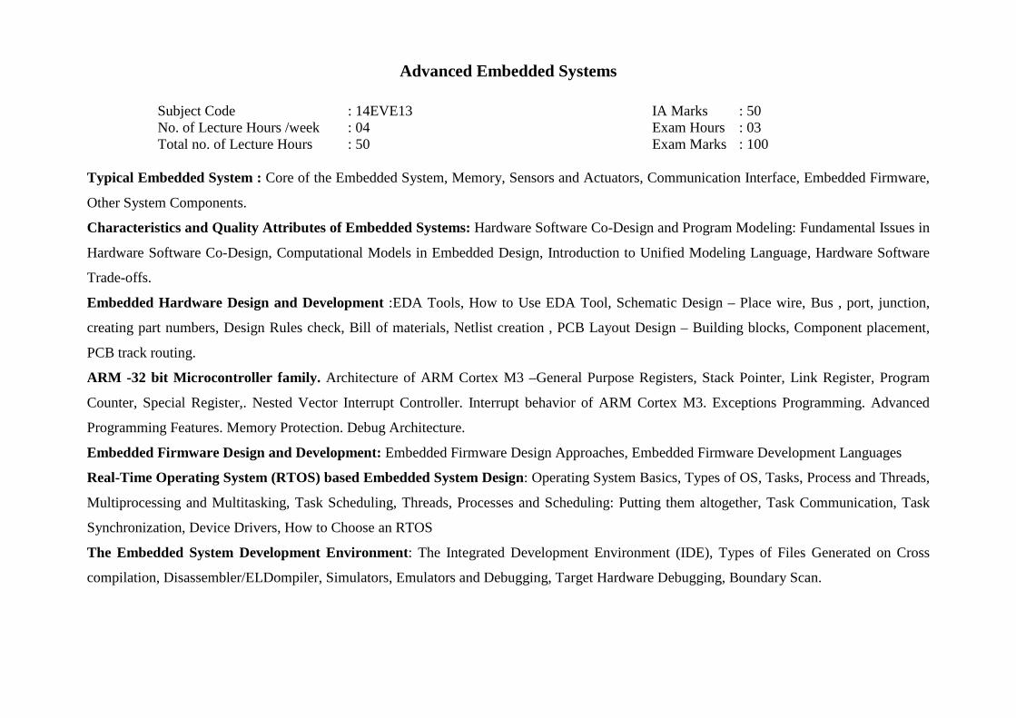
Advanced Embedded Systems
Subject Code : 14EVE13 IA Marks : 50 No. of Lecture Hours /week : 04 Exam Hours : 03 Total no. of Lecture Hours : 50 Exam Marks : 100
Typical Embedded System : Core of the Embedded System, Memory, Sensors and Actuators, Communication Interface, Embedded Firmware,
Other System Components.
Characteristics and Quality Attributes of Embedded Systems: Hardware Software Co-Design and Program Modeling: Fundamental Issues in
Hardware Software Co-Design, Computational Models in Embedded Design, Introduction to Unified Modeling Language, Hardware Software
Trade-offs.
Embedded Hardware Design and Development :EDA Tools, How to Use EDA Tool, Schematic Design – Place wire, Bus , port, junction,
creating part numbers, Design Rules check, Bill of materials, Netlist creation , PCB Layout Design – Building blocks, Component placement,
PCB track routing.
ARM -32 bit Microcontroller family. Architecture of ARM Cortex M3 –General Purpose Registers, Stack Pointer, Link Register, Program
Counter, Special Register,. Nested Vector Interrupt Controller. Interrupt behavior of ARM Cortex M3. Exceptions Programming. Advanced
Programming Features. Memory Protection. Debug Architecture.
Embedded Firmware Design and Development: Embedded Firmware Design Approaches, Embedded Firmware Development Languages
Real-Time Operating System (RTOS) based Embedded System Design: Operating System Basics, Types of OS, Tasks, Process and Threads,
Multiprocessing and Multitasking, Task Scheduling, Threads, Processes and Scheduling: Putting them altogether, Task Communication, Task
Synchronization, Device Drivers, How to Choose an RTOS
The Embedded System Development Environment: The Integrated Development Environment (IDE), Types of Files Generated on Cross
compilation, Disassembler/ELDompiler, Simulators, Emulators and Debugging, Target Hardware Debugging, Boundary Scan.

Reference Books:
1. Shibu K V, “Introduction to Embedded Systems”, Tata McGraw Hill Education Private Limited, 2009
2. Joseph Yiu, “The Definitive Guide to the ARM Cortex-M3” , Newnes, (Elsevier), 2008.
3. James K Peckol, “Embedded Systems – A contemporary Design Tool”, John Weily, 2008.
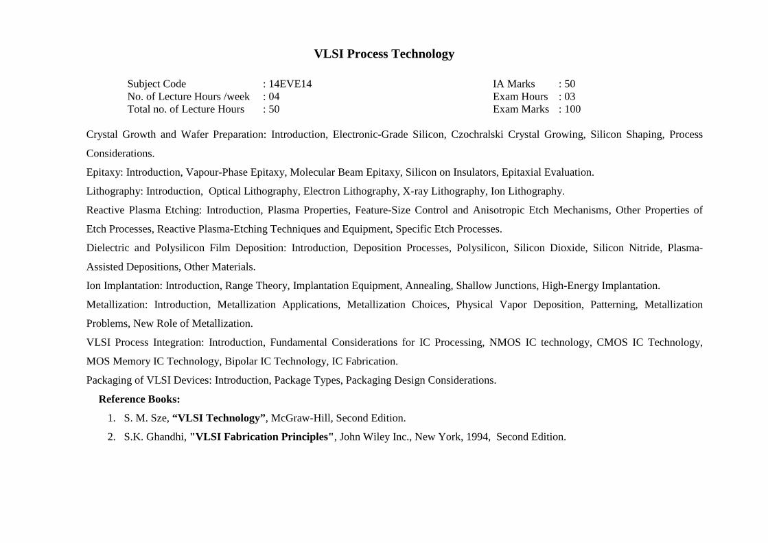
VLSI Process Technology
Subject Code : 14EVE14 IA Marks : 50 No. of Lecture Hours /week : 04 Exam Hours : 03 Total no. of Lecture Hours : 50 Exam Marks : 100
Crystal Growth and Wafer Preparation: Introduction, Electronic-Grade Silicon, Czochralski Crystal Growing, Silicon Shaping, Process
Considerations.
Epitaxy: Introduction, Vapour-Phase Epitaxy, Molecular Beam Epitaxy, Silicon on Insulators, Epitaxial Evaluation.
Lithography: Introduction, Optical Lithography, Electron Lithography, X-ray Lithography, Ion Lithography.
Reactive Plasma Etching: Introduction, Plasma Properties, Feature-Size Control and Anisotropic Etch Mechanisms, Other Properties of
Etch Processes, Reactive Plasma-Etching Techniques and Equipment, Specific Etch Processes.
Dielectric and Polysilicon Film Deposition: Introduction, Deposition Processes, Polysilicon, Silicon Dioxide, Silicon Nitride, Plasma-
Assisted Depositions, Other Materials.
Ion Implantation: Introduction, Range Theory, Implantation Equipment, Annealing, Shallow Junctions, High-Energy Implantation.
Metallization: Introduction, Metallization Applications, Metallization Choices, Physical Vapor Deposition, Patterning, Metallization
Problems, New Role of Metallization.
VLSI Process Integration: Introduction, Fundamental Considerations for IC Processing, NMOS IC technology, CMOS IC Technology,
MOS Memory IC Technology, Bipolar IC Technology, IC Fabrication.
Packaging of VLSI Devices: Introduction, Package Types, Packaging Design Considerations.
Reference Books:
1. S. M. Sze, “VLSI Technology” , McGraw-Hill, Second Edition.
2. S.K. Ghandhi, "VLSI Fabrication Principles" , John Wiley Inc., New York, 1994, Second Edition.

Digital System Design Using Verilog
Subject Code : 14 ELD151 IA Marks : 50 No. of Lecture Hours /week : 04 Exam Hours : 03 Total no. of Lecture Hours : 50 Exam Marks : 100
Introduction and Methodology: Digital Systems and Embedded Systems, Binary representation and Circuit Elements, Real-World Circuits,
Models, Design Methodology.
Combinational Basics: Boolean Functions and Boolean Algebra, Binary Coding, Combinational
Components and Circuits, Verification of Combinational Circuits.
Number Basics: Unsigned and Signed Integers, Fixed and Floating-point Numbers.
Sequential Basics: Storage elements, Counters, Sequential Datapaths and Control, Clocked Synchronous Timing Methodology.
Memories: Concepts, Memory Types, Error Detection and Correction.
Implementation Fabrics: ICs, PLDs, Packaging and Circuit Boards, Interconnection and Signal Integrity.
Processor Basics: Embedded Computer Organization, Instruction and Data, Interfacing with memory.
I/O interfacing : I/O devices, I/O controllers, Parallel Buses, Serial Transmission, I/O software.
Accelerators: Concepts, case study, Verification of accelerators.
Design Methodology: Design flow, Design optimization, Design for test.
REFERENCE BOOKS:
1. Peter J. Ashenden, “Digital Design: An Embedded Ssytems Approach Using VERILOG” , Elesvier, 2010.

VLSI Design Automation
Subject Code : 14EVE152 IA Marks : 50 No. of Lecture Hours /week : 04 Exam Hours : 03 Total no. of Lecture Hours : 50 Exam Marks : 100
Logic Synthesis & Verification: Introduction to combinational logic synthesis, Binary Decision Diagram, Hardware models for High-level
synthesis.
VLSI Automation Algorithms : Partitioning: problem formulation, classification of partitioning algorithms, Group migration algorithms,
simulated annealing & evolution, other partitioning algorithms.
Placement, Floor Planning & Pin Assignment: problem formulation, simulation base placement algorithms, other placement algorithms,
constraint based floor planning, floor planning algorithms for mixed block & cell design. General & channel pin assignment
Global Routing: Problem formulation, classification of global routing algorithms, Maze routing algorithm, line probe algorithm, Steiner Tree
based algorithms, ILP based approaches
Detailed Routing: problem formulation, classification of routing algorithms, single layer routing algorithms, two layer channel routing
algorithms, three layer channel routing algorithms, and switchbox routing algorithms.
Over The Cell Routing & Via Minimization : two layers over the cell routers, constrained & unconstrained via minimization
Scripting Languages : Overview of Scripting Languages – PERL, CGI, VB Script, Java Script. PERL: Operators, Statements Pattern Matching
etc. Data Structures, Modules, Objects, Tied Variables. Inter process Communication Threads, Compilation & Line Interfacing
REFERENCE BOOKS:
1. Naveed Shervani, “Algorithms for VLSI physical design Automation” , Kluwer Academic Publisher, Second edition.
2. Christophn Meinel & Thorsten Theobold, “Algorithm and Data Structures for VLSI Design” , KAP, 2002.
3. Rolf Drechsheler : “Evolutionary Algorithm for VLSI” , Second edition
4. Trimburger, “Introduction to CAD for VLSI”, Kluwer Academic publisher, 2002
5. Randal L, Schwartz Tom Phoenix, “Learning PERL” , Oreilly Publications, 3rd Edn., 2000

6. Larry Wall, Tom Christiansen, John Orwant, “Programming PERL” , Oreilly Publications, 3rd
7. Edn., 2000.
8. Tom Christiansen, Nathan Torkington, “PERL Cookbook” , Oreilly Publications, 3rd Edn,2000
NanoElectronics
Subject Code : 14ELD153 IA Marks : 50 No. of Lecture Hours /week : 04 Exam Hours : 03 Total no. of Lecture Hours : 50 Exam Marks : 100
Introduction: Overview of nanoscience and engineering. Development milestones in microfabrication and electronic industry. Moores law and
continued miniaturization., Classification of Nanostructures, Electronic properties of atoms and solids: Isolated atom, Bonding between atoms,
Giantmolecular solids, Free electron models and energy bands, crystalline solids, Periodicity of crystal lattices, Electronic conduction, effects of
nanometerlength scale, Fabrication methods: Top down processes, Bottom up processes methods for templating the growth of nanomaterials,
ordering of nanosystems.
Characterization: Classification, Microscopic techniques, Field ion microscopy, scanning probe techniques, diffraction techniques: bulk,
surface, spectroscopy techniques: photon, radiofrequency, electron, surface analysis and dept profiling: electron, mass, Ion beam,
Reflectrometry, Techniques for property measurement: mechanical, electron, magnetic, thermal properties.
Inorganic semiconductor nanostructures: overview of semiconductor physics. Quantum confinement in semiconductor nanostructures:
quantumwells, quantum wires, quantum dots, super-lattices, band offsets, electronicdensity of states.
Fabrication techniques: requirements of ideal semiconductor, epitaxial growth of quantum wells, lithography and etching, cleaved edgeover
growth, growth of vicinal substrates, strain induced dots and wires, electrostatically induced dots and wires, Quantum well width fluctuations,
thermally annealed quantum wells, semiconductor nanocrystals, collidal quantum dots, self-assembly techniques.
Physical processes: modulation doping, quantum hall effect, resonanttunneling, charging effects, ballistic carrier transport, Inter band
absorption, intraband absorption, Light emission processes, phonon bottleneck, quantumconfined stark effect, nonlinear effects, coherence and
dephasing, characterization of semiconductor nanostructures: optical electrical and structural.
Methods of measuring properties:structure:atomic,crystallography,microscopy,spectroscopy. Properties of nanoparticles: metalnano clusters,
semiconducting nanoparticles, rare gas and molecularclusters, methods of synthesis(RF, chemical, thermolysis, pulsed laser methods) Carbon
nanostructures and its applications(field emission and shielding, computers, fuelcells, sensors, catalysis).Self assembling nanostructured
molecular materials and devices: building blocks, principles of self assembly, methods to prepare and pattern nanoparticles, template
dnanostructures, liquid crystal mesophases. Nanomagnetic materials and devices: magnetism, materials, magnetoresistance, nanomagnetism
intechnology, challenges facing nanomagnetism.
Applications: Injectionlasers, quantumcascadelasers, singlephotonsources, biologicaltagging, opticalmemories, coulomb blockade devices,
photonic structures, QWIP’s, NEMS, MEMS.
Reference Books:
1. Ed Robert Kelsall,IanHamley,MarkGeoghegan, “ Nanoscale science and technology” ,John wiley and sons,2007.
2. Charles P Poole,Jr,Frank J owens, “Introduction to Nanotechnology” ,John wiley,copyright 2006,Reprint 2011.
3. Ed William A Goddard III,Donald W Brenner,Sergey EdwardLyshevski,Gerald J Lafrate, “ Hand Book of Nanoscience Engineering
and Technology” ,CRC press,2003

ASIC Design
Subject Code : 14EVE154 IA Marks : 50 No. of Lecture Hours /week : 04 Exam Hours : 03 Total no. of Lecture Hours : 50 Exam Marks : 100
Note: All Designs Will Be Based On VHDL Introduction : Full Custom with ASIC, Semi custom ASICS, Standard Cell based ASIC, Gate array based ASIC, Channelled gate array, Channel
less gate array, structured get array, Programmable logic device, FPGA design flow, SIC cell libraries.
Data Logic Cells: Data Path Elements, Adders, Multiplier, Arithmetic Operator, I/O cell, Cell Compilers
ASIC Library Design : Logical effort: practicing delay, logical area and logical efficiency logical paths, multi stage cells, optimum delay,
optimum no. of stages, library cell design.
Low-Level Design Entry: Schematic Entry: Hierarchical design. The cell library, Names, Schematic, Icons & Symbols, Nets, schematic entry
for ASIC’S, connections, vectored instances and buses, Edit in place attributes, Netlist, screener, Back annotation.
Programmable ASIC: programmable ASIC logic cell, ASIC I/O cell.
A Brief Introduction to Low Level Design Language: an introduction to EDIF, PLA Tools, an introduction to CFI designs representation. Half
gate ASIC. Introduction to Synthesis and Simulation.
ASIC Construction Floor Planning and Placement And Routing: Physical Design, CAD Tools, System Partitioning, Estimating ASIC size,
partitioning methods. Floor planning tools, I/O and power planning, clock planning, placement algorithms, iterative placement improvement,
Time driven placement methods. Physical Design flow global Routing, Local Routing, Detail Routing, Special Routing, Circuit Extraction and
DRC.
Reference Books:
1. M.J.S .Smith, - “Application - Specific Integrated Circuits” – Pearson Education, 2003.
2. Jose E.France, YannisTsividis, “Design of Analog-Digital VLSICircuits for Telecommunication and signal processing”, Prentice
Hall, 1994.

3. MalcolmR.Haskard; Lan. C. May, “Analog VLSI Design - NMOSand CMOS”, Prentice Hall, 1998.
4. Mohammed Ismail and Terri Fiez, “Analog VLSI Signal andInformation Processing”, McGraw Hill, 1994
System Verilog
Subject Code : 14 EVE155 IA Marks : 50 No. of Lecture Hours /week : 04 Exam Hours : 03 Total no. of Lecture Hours : 50 Exam Marks : 100
Basics of Verification: Difference between ASIC verification and ASIC testing, Verification basics, Testbenches, Layered Organization of
Testbenches. Importance of hardware verification languages and methodologies. (Reference website/Verilog Books / SystemVerilog
Methodologies )
System Verilog data types and typedefs: System Verilog data types, enhanced literal numbers syntax, 4-state and 2-state types, typedefs,
enum, struct data type, Type parameters, $unit and $root. Packages, strings, static and dynamic type casting, Random number generation.
(Reference 1)
System Verilog operators, loops, jumps, functions: loops and jumps in system verilog, introduction to different always blocks, systemverilog
enhancements to tasks and functions, systemverilog priority and unique modifiers for case and if statements, ‘time scale, systemverilog timeunit
and time precision (Reference 1)
Structs, Unions, Packed and Unpacked Arrays, Semaphores and Mailboxes:
Structs and its assignments, packed and unpacked arrays, array indexing, structs and packed structs, Unions and packed unions, dynamic arrays
and methods, foreach loop, associative arrays and methods, queues and concatenation operations, queue methods, semaphores and methods,
mailboxes and methods, bounded and unbounded mailboxes. (Reference 1)
Class and Randomization: Systemverilog class basics, class declaration, class members and methods, class handles, class object construction,
super and this keywords, object handles, user defined constructors, class extension and inheritance, chaining new() constructors, overriding class
methods, extending class methods, local and protected keywords, constrained random variables, directed vs random testing, rand and randc class
data types, randomize-randomizing class variables, random case, built-in-randomization methods, random sequence and examples. (Reference1)
Interfaces: Interface overview, generic interfaces, interfaces vs records, how interfaces work, requirements of good interface, interface
constructs, interface mode ports. (Reference 1)
Program block: Fundamental testbench construction, program blocks, program block interaction with modules, final blocks, Testbench

stimulus/Verification vector timing strategies. (Reference 1)
Clocking: Clocking blocks, clocking skews, clocking block scheduling, fork-join processes. (Reference 1)
Constrained Random variables, Coverage, Methods and interfaces:
Randomization constraints, simple and multi-statement constraints, constraint distribution and set membership, constraint distribution operators,
external constraints, covergroups, coverpoints, coverpoint bins and labels, cross coverage, covergroup options, coverage capabilities. Virtual
class, why to use virtual class, virtual class methods and restrictions, polymorphism using virtual methods, pure virtual methods, pure
constraints, passing type parameters, virtual interfaces. (Reference 1)
System Verilog assertions: Assertion definition, assertion benefits, system Verilog assertion types, immediate assertions, concurrent assertions,
assert and cover properties and labels, overlapping and non-overlapping implications, edge testing functions, sequences, Vacuous success,
property styles, System Verilog assertion system functions, Assertion severity tasks, assertion and coverage example of an FSM design.
(Reference 3)
References: 1. Christian B Spear, “ SystemVerilog for Verification: A guide to learning the Testbench language features”, Springer publications, 3 rd edition.
2. VijayaRaghavan, “SystemVerilog Assertions”, Springer publications, 2005
3. Sutherland, “ Systemverilog for Design”, Springer publications

VLSI Design and Embedded System Lab -1
Subject Code : 14EVE16 IA Marks : 50 No. of Lecture Hours /week : 03 Exam Hours : 03 Total no. of Lecture Hours : 42 Exam Marks : 50
VLSI Digital Design
ASIC-Digital Design Flow
1. Write Verilog Code for the following circuits and their Test Bench for verification, observe the waveform and synthesize the code with
technological library(constraints to be given). Do the initial timing verification with gate level simulation.
1.Aninverter,Buffer and Transmission gate
2.Basic/universal gates
3.Flip flop -RS, D, JK, MS, T
4.Serial & Parallel adder
5.4-bit counter [Synchronous & Asynchronous counter]
FPGA DIGITAL DESIGN
VLSI Front End Design programs:
Programming can be done using any complier. Down load the programs on FPGA/CPLD boards and performance testing may be done using
pattern generator (32 channels and logic analyzer )/Chipscope pro apart from verification by simulation with any of the front end tools
1. Write Verilog code for the design of 8-bit
i. Carry Ripple Adder
ii. Carry LookAhead adder
iii.Carry Skip Adder
iv.BCD Adder & Subtracter
2. Write Verilog Code for 8-bit
i. Array Multiplication (Signed and Unsigned)
ii. Booth Multiplication (Radix-4)
3. Write Verilog code for 4/8-bit
i. Magnitude Comparator
ii. LFSR
iii.Parity Generator
iv.Universal Shift Register
4. Write Verilog Code for 3-bit Arbitary Counter to generate 0,1,2,3,6,5,7 and repeats.
5. Design a Mealy and Moore Sequence Detector using Verilog to detect Sequence.
Eg 11101 (with and without overlap) any sequence can be specified
6. Design a FIFO and LIFO buffers in Verilog and Verify its Operation.
7. Design a coin operated public Telephone unit using Mealy FSM model with following operations
i. The calling process is initiated by lifting the receiver.
ii. Insert 1 Rupee Coin to make a call.
iii. If line is busy, placing the receiver on hook should return a coin
iv. If line is through, the call is allowed for 60 seconds at the 45th second prompt another 1 Rupee coin to be inserted, to continue the call.
v. If user doesn't insert the coin within 60 seconds the call should be terminated.
vi. The system is ready to accept new call request when the receiver is placed on the hook.
vii. The FSM goes 'out of order' state when there is a Line Fault.
Note: Implementing the above designs on Xilinx/Altera/Cypress/equivalent based FPGA/CPLD kits
Embedded Systems:
1.Use any EDA (Electronic Design Automation) tool to learn the Embedded Hardware Design and for PCB design.
2.Familiarize the different entities for the circuit diagram design.
3.Familiarize with the layout design tool, building blocks, component placement, routings, design rule checking etc.
ARM-CORTEX M3
[Programming to be done using Keiluvision 4 and download the program on to a M3 evaluation board such as NXP LPC1768 or
ATMEL ATSAM3U].
1. Write an Assembly language program to calculate 10+9+8+.........+1
2. Write a Assembly language program to link Multiple object files and link them together.
3. Write a Assembly language program to store data in RAM.
4. Write a C program to Output the "Hello World" message using UART.
5. Write a C program to Design a Stopwatch using interrupts.
6.Write an Exception vector table in C
7. Write an Assembly Language Program for locking a Mutex.
8. Write a SVC handler in C. Use the wrapper code to extract the correct stack frame starting location. The C handler can then use this to extract
the stacked PC location and the stacked register values.

Design of Analog and Mixed Mode VLSI Circuits
Subject Code : 14 EVE21 IA Marks : 50 No. of Lecture Hours /week : 04 Exam Hours : 03 Total no. of Lecture Hours : 50 Exam Marks : 100
Basic MOS Device Physics: General considerations, MOS I/V Characteristics, second order effects, MOS device models.
Single stage Amplifier: CS stage with resistance load, divide connected load, current source load, triode load, CS stage with source
degeneration, source follower, common-gate stage, cascade stage, choice of device models.
Frequency response of CS stage: source follower, Common gate stage, Cascade stage and Difference pair. Noise in CS stage, C- G stage,
source follower, cascade stage, differential pair.
Differential Amplifiers & Current Mirrors: Basic difference pair, common mode response, Differential pair with MOS loads, Gilbert cell.
Basic current mirrors, Cascade mirrors, active current mirrors.
Operational Amplifiers: One Stage OP-Amp. Two Stage OP-Amp, Gain boosting, Common Mode Feedback, Slew rate, Power Supply
Rejection, Noise in Op Amps.
Oscillators and Phase Locked Loops: Ring Oscillators, LC Oscillators, VCO, Mathematical Model of VCO.
Simple PLL, Charge pump PLL, Non-ideal effects in PLL, Delay locked loops and applications.
Bandgap Refernces and Switched capacitor Circuits: General Considerations, Supply Independent biasing, PTAT Current Generation, Constant
Gm Biasing, Sampling Switches, Switched Capacitor Amplifiers.
Data Converter Architecturres: DAC & ADC Specifications, Resistor String DAC, R-2R Ladder Network, Current Steering DAC, Charge
Scaling DAC, Cyclic DAC, Pipeline DAC, Flash ADC, Pipeline ADC, Integrating ADC, Successive Approximation ADC.
Reference Book:
1. “Design of Analog CMOS Integrated Circuits”, Behzad Razavi, TMH, 2007.

Low Power VLSI Design
Subject Code : 14 EVE22 IA Marks : 50 No. of Lecture Hours /week : 04 Exam Hours : 03 Total no. of Lecture Hours : 50 Exam Marks : 100
Introduction: Need for low power VLSI chips, Sources of power dissipation on Digital Integrated circuits. Emerging Low power approaches,
Physics of power dissipation in CMOS devices.
Device & Technology Impact on Low Power: Dynamic dissipation in CMOS, Transistor sizing & gate oxide thickness, Impact of technology
Scaling, Technology & Device innovation.
Power estimation, Simulation Power analysis: SPICE circuit simulators, gate level logic simulation, capacitive power estimation, static state
power, gate level capacitance estimation, architecture level analysis, data correlation analysis in DSP systems, Monte Carlo simulation.
Probabilistic power analysis: Random logic signals, probability & frequency, probabilistic power analysis techniques, signal entropy.
Low Power Design Circuit level: Power consumption in circuits. Flip Flops & Latches design, high capacitance nodes, low power digital cells
library.
Logic level: Gate reorganization, signal gating, logic encoding, state machine encoding, pre-computation logic.
Low power Architecture & Systems: Power & performance management, switching activity reduction, parallel architecture with voltage
reduction, flow graph transformation, low power arithmetic components, low power memory design.
Low power Clock Distribution: Power dissipation in clock distribution, single driver Vs distributed buffers, Zero skew Vs tolerable skew, chip
& package co design of clock network.
Algorithm & Architectural Level Methodologies: Introduction, design flow, Algorithmic level analysis & optimization, Architectural level
estimation & synthesis.
Reference Books:
1. Kaushik Roy, Sharat Prasad, “Low-Power CMOS VLSI Circuit Design” Wiley, 2000
2. Gary K. Yeap, “Practical Low Power Digital VLSI Design”, KAP, 2002

3. Rabaey, Pedram, “Low Power Design Methodologies” Kluwer Academic, 1997

VLSI Testing and Verification
Subject Code : 14 EVE23 IA Marks : 50 No. of Lecture Hours /week : 04 Exam Hours : 03 Total no. of Lecture Hours : 50 Exam Marks : 100
Introduction to Testing: Testing Philosophy, Role of Testing, Digital and Analog VLSI Testing, VLSI Technology Trends Affecting Testing.
Faults in Digital Circuits: Failures and Faults, Modeling of Faults, Temporary Faults.
Test Generation for Combinational Logic Circuits: Fault Diagnosis of Digital Circuits, Test Generation Techniques for Combinational
Circuits, Detection of Multiple Fauls in Combinational Logic Circuits.
Design of Testable Sequential Circuits: Controllability and Observability, Ad Hoc Design Rules for Improving Testability, Design of
Dignosable Sequential Circuits, The Scan-Path Technique for Testable Sequential Circuit Design, Level-Sensitive Scan Design, Random Access
Scan Technique, Partial Scan, Testable Sequential Circuit Design Using Nonscan Techniques, CrossCheck, Boundry Scan.
Built-In Self Test: Test Pattern Generation for BIST, Output Response Analysis, Circular BIST, BIST Architectures.
Testable Memory Design: RAM Fault Models, Test Algorithms for RAMs, Detection of Pattern Sensitive Faults, BIST Techniques for Ram
Chips, Test Generation and BIST for Embedded RAMs.
Importance of Design Verification: What is verification? What is attest bench? The importance of verification, Reconvergence model, Formal
verification, Equivalence checking, Model checking, Functional verification.[Ref4- Chapter1]
Verification Tools: Linting tools: Limitations of linting tools, linting verilog source code, linting VHDL source code, linting OpenVera and e-
source code, code reviews. Simulators: Stimulus and response, Event based simulation, cycle based simulation, Co-simulators, verification
intellectual property: hardware modelers, waveform viewers.[Ref4-Chapter2]
The verification plan: The role of verification plan: specifying the verification plan, defining the first success. Levels of verification: unit level
verification, reusable components verification, ASIC and FPGA verification, system level verification, board level verification, verifying
strategies, verifying responses. [Ref4-Chapter3]

Static Timing Verification : Concept of static timing analysis. Cross talk and noise. Limitations of STA. slew of a wave form, Skew between the
signals, Timing arcs and unateness, Min and Max timing paths, clock domains, operating conditions, critical path analysis, falsepaths, Timing
models. [Ref5 Chapter 1, 2, 3, 8]
Physical Design Verification: Layout rule checks and electrical rule checks. Parasitic extraction. Antenna, Crosstalk and Noise: Cross talk
glitch analysis, crosstalk delayanalysis, timing verification [Ref6 Chapter 8]
Reference Books:
1. P. K. Lala, “Digital Circuit Testing and Testability” , Academic Press
2. M.L. Bushnell and V.D. Agrawal, “Essentials of Electronic Testing for Digital, Memory and Mixed-Signal VLSI Circuits” , Kluwar
Academic Publishers.
3. M. Abramovici, M.A. Breuer and A.D. Friedman, "Digital Systems and Testable Design", Jaico Publishing House, 2002.
4. JanickBergeron, “Writing testbenches: functional verification of HDL models”, 2nd edition ,Kluwer Academic Publishers,2003
5. JayaramBhasker,RakeshChadha ,“Static Timing Analysis for Nanometer Designs” A practical approach, Springer publications
6. PrakashRashinkar, PeterPaterson,Leena Singh “System on a Chip Verification”, Kulwer Publications.
7. http://www.cse.psu.edu/~vijay/verify/instructors.html

Real Time Operating Systems
Subject Code : 14 ELD24 IA Marks : 50 No. of Lecture Hours /week : 04 Exam Hours : 03 Total no. of Lecture Hours : 50 Exam Marks : 100
Introduction to Real-Time Embedded Systems: Brief history of Real Time Systems, A brief history of Embedded Systems.
System Resources: Resource Analysis, Real-Time Service Utility, Scheduling Classes, The Cyclic Executive, Scheduler Concepts, Preemptive
Fixed Priority Scheduling Policies, Real-Time OS, Thread Safe Reentrant Functions.
Processing: Preemptive Fixed-Priority Policy, Feasibility, Rate Monotonic least upper bound, Necessary and Sufficient feasibility, Deadline –
Monotonic Policy, Dynamic priority policies.
I/O Resources: Worst-case Execution time, Intermediate I/O, Execution efficiency, I/O Architecture.
Memory: Physical hierarchy, Capacity and allocation, Shared Memory, ECC Memory, Flash file systems.
Multi-resource Services: Blocking, Deadlock and livestock, Critical sections to protect shared resources, priority inversion
Soft Real-Time Services: Missed Deadlines, QoS, Alternatives to rate monotonic policy, Mixed hard and soft real-time services.
Embedded System Components: Firmware components, RTOS system software mechanisms, Software application components.
Debugging Components: Execptions assert, Checking return codes, Single-step debugging, kernel scheduler traces, Test access ports, Trace
ports, Power-On self test and diagnostics, External test equipment, Application-level debugging.
Performance Tuning: Basic concepts of drill-down tuning, hardware – supported profiling and tracing, Building performance monitoring into
software, Path length, Efficiency, and Call frequency, Fundamental optimizations.
High availability and Reliability Design: Reliability and Availability, Similarities and differences, Reliability, Reliable software, Available
software, Design tradeoffs, Hierarchical applications for Fail-safe design.
Design of RTOS – PIC microcontroller. (Chap 13 of book Myke Predko)
Reference Books:
1. “Real-Time Embedded Systems and Components”, Sam Siewert, Cengage Learning India Edition, 2007.

2. “Programming and Customizing the PIC microcontroller”, Myke Predko, 3rd Ed, TMH, 2008.
3. “Programming for Embedded Systems”, Dreamtech Software Team, Jhon Wiley, India Pvt. Ltd., 2008.

VLSI for Signal Processing
Subject Code : 14 EVE251 IA Marks : 50 No. of Lecture Hours /week : 04 Exam Hours : 03 Total no. of Lecture Hours : 50 Exam Marks : 100
Introduction to DSP systems: Typical DSP Algorithms, DSP Application Demands And Scaled CMOS Technologies, Representations Of DSP
Algorithms.
Iteration Bounds: Data flow graph Representations, loop bound and Iteration bound, Algorithms for Computing Iteration Bound, Iteration
Bound of multi rate data flow graphs.
Pipelining and parallel processing, pipelining of FIR Digital Filters, parallel processing, Pipelining and parallel processing for low power.
Retiming: Definition and Properties, Solving Systems of Inequalities, Retiming Techniques, Unfolding An Algorithm for Unfolding, Properties
Of Unfolding, Critical path, Unfolding And Retiming, Application of Unfolding
Systolic architecture design: systolic array design Methodology, FIR systolic array, Selection of Scheduling Vector, Matrix-Matrix
Multiplication and 2D systolic Array Design, Systolic Design for space representation containing Delays.
Fast convolution–Cook-Toom Algorithm, Winograd Algorithm, Iterated convolution, cyclic Convolution Design of fast convolution Algorithm
by Inspection
Pipelined and Parallel recursive and adaptive filter: Pipeline Interleaving in Digital Filter, first order IIR digital Filter, Higher order IIR
digital Filter, parallel processing for IIR filter, Combined pipelining and parallel processing for IIR Filter, Low power IIR Filter Design Using
Pipe lining and parallel processing, pipelined Adaptive digital filter.
Reference Books:
1. KeshabK.Parthi, " VLSI Digital Signal Processing systems, Design and implementation ", Wiley, Inter Science, 1999.
2. Mohammed Isamail and Terri Fiez, " Analog VLSI Signal and Information Processing ", Mc Graw-Hill,1994.
3. S.Y. Kung, H.J. White House, T. Kailath, " VLSI and Modern Signal Processing ", Prentice Hall, 1985.
4. Jose E. France, YannisTsividis, " Design of Analog - Digital VLSI Circuits for Telecommunication and Signal Processing ", Prentice
Hall, 1994

High Speed VLSI Design
Subject Code : 14 EVE252 IA Marks : 50 No. of Lecture Hours /week : 04 Exam Hours : 03 Total no. of Lecture Hours : 50 Exam Marks : 100
Introduction to high speed digital design: Frequency, time and distance issues in digital VLSI design. Capacitance and inductance effects, high
speed properties of logic gates, speed and power. Modeling of wires, geometry and electrical properties of wires, Electrical models of wires,
transmission lines, lossless LC transmission lines, lossy RLC transmission lines and special transmission lines.
Power distribution and Noise: Power supply network, local power regulation, IR drops, area bonding. On-chip bypass capacitors and symbiotic
bypass capacitors. Power supply isolation. Noise sources in digital systems, power supply noise, crosstalk and inter symbol interference.
Signaling convention and circuits: Signaling modes for transmission lines, signaling over lumped transmission media, signaling over RC
interconnect, driving lossy LC lines, simultaneous bi-directional signaling terminations, transmitter and receiver circuits.
Timing convention and synchronisation: Timing fundamentals, timing properties of clocked storage elements, signals and events, open loop
timing, level sensitive clocking, pipeline timing, closed loop timing, clock distribution, synchronization failure and meta-stability, clock
distribution, clock skew and methods to reduce clock skew, controlling crosstalk in clock lines, delay adjustments, clock oscillators and clock
jitter - PLL and DLL based clock aligners.
Clocked & non clocked Logics:
Single-Rail Domino Logic, Dual-Rail Domino Structures, Latched Domino Structures, Clocked Pass GateLogic, Static CMOS, DCVS Logic,
Non-Clocked Pass Gate Families.
Latching Strategies:
Basic Latch Design, and Latching single-ended logic and Differential Logic,
Race Free Latches for Pre-charged Logic Asynchronous Latch Techniques
Reference Books:
1. William S. Dally & John W. Poulton, “Digital Systems Engineering”, Cambridge University Press, 1998.

2. Kerry Bernstein & et. Al., “High Speed CMOS Design Styles”, Kluwer, 1999.
3. Howard Johnson & Martin Graham, “High Speed Digital Design” A Handbook of Black Magic, Prentice Hall PTR, 1993.
4. Masakazu Shoji, “High Speed Digital Circuits” , Addison Wesley Publishing Company, 1996.
5. Jan M, Rabaey, et al, “Digital Integrated Circuits”, A Design Perspective, Pearson, 2003.

MEMS
Subject Code : 14ELD253 IA Marks : 50 No. of Lecture Hours /week : 04 Exam Hours : 03 Total no. of Lecture Hours : 50 Exam Marks : 100
Overview of MEMS & Microsystems: MEMS & Microsystems, Typical MEMS and Micro system products — features of MEMS, The
multidisciplinary nature of Microsystems design and manufacture, Applications of Microsystems in automotive industry, health care industry,
aerospace industry, industrial products, consumer products and telecommunications.
Scaling Laws in Miniaturization: Introduction to scaling, scaling in geometry, scaling in rigid body dynamics, scaling electrostatic forces,
electromagnetic forces, electricity, scaling in fluid mechanics & heat transfer.
Transduction Principles in MEMS & Microsystems: Introduction, Micro sensors — thermal, radiation, mechanical, magnetic and bio —
sensors, Micro actuation, MEMS with micro actuators.
Microsystems Fabrication Process: Introduction, Photolithography, Ion-implantation, diffusion, oxidation, CVD, PVD, etching and materials
used for MEMS, Some MEMS fabrication processes: surface micro-machining, bulk micromachining, LIGA process, LASER micro
machining, MUMPS, FAB-less fabrication.
Micro System Design and Modeling: Introduction, Design considerations: Process design, Mechanical design, Modeling using CAD tools:
ANSYS / Multiphysics or Intellisuite or MEMS CAD, Features and Design considerations of RF MEMS, Design considerations of Optical
MEMS (MOEMS), Design and Modeling: case studies - i) Cantilever beam ii) Micro switches iii) MEMS based SMART antenna in mobile
applications for maximum reception of signal in changing communication conditions and iv) MEMS based micro mirror array for control and
switching in optical communications.
Micro system packaging: Over view of mechanical packaging of micro electronics micro system packaging, Interfaces in micro system
packaging, Packaging technologies.
Reference Books
1. Tai — Ran Hsu, “MEMS and Micro Systems : Design and Manufacture”, Tata McGraw Hill, 2002

2. Boca Raton, “MEMS and NEMS: Systems, Devices and Structures”, CRC Press, 2002
3. J. W. Gardner and V. K. Vardan, “Micro Sensors MEMS and SMART Devices”, John Wiley, 2002
4. N. Maluf “Introduction to Micro Mechanical Systems Engineering, Artech House”, Norwood, MA, 2000.

CMOS RF Circuit Design
Subject Code : 14 EVE254 IA Marks : 50 No. of Lecture Hours /week : 04 Exam Hours : 03 Total no. of Lecture Hours : 50 Exam Marks : 100
Introduction to RF Design and Wireless Technology: Design and Applications, Complexity and Choice of Technology. Basic concepts in RF
design: Nonlinearly and Time Variance, Intersymbol interference, random processes and noise. Sensitivity and dynamic range, conversion of
gains and distortion
RF Modulation: Analog and digital modulation of RF circuits, Comparison of various techniques for power efficiency, Coherent and non-
coherent detection, Mobile RF communication and basics of Multiple Access techniques. Receiver and Transmitter architectures, Direct
conversion and two-step transmitters
RF Testing: RF testing for heterodyne, Homodyne, Image reject, Direct IF and sub sampled receivers.
BJT and MOSFET Behavior at RF Frequencies: BJT and MOSFET behavior at RF frequencies, modeling of the transistors and SPICE
model, Noise performance and limitations of devices, integrated parasitic elements at high frequencies and their monolithic implementation
RF Circuits Design: Overview of RF Filter design, Active RF components & modeling, Matching and Biasing Networks. Basic blocks in RF
systems and their VLSI implementation, Low noise Amplifier design in various technologies, Design of Mixers at GHz frequency range,
Various mixers- working and implementation. Oscillators- Basic topologies VCO and definition of phase noise, Noise power and trade off.
Resonator VCO designs, Quadrature and single sideband generators. Radio frequency Synthesizers- PLLS, Various RF synthesizer architectures
and frequency dividers, Power Amplifier design, Liberalization techniques, Design issues in integrated RF filters.
Reference Books:
B. Razavi, “RF Microelectronics” PHI 1998
R. Jacob Baker, H.W. Li, D.E. Boyce “CMOS Circuit Design, layout and Simulation”, PHI 1998.
Thomas H. Lee “Design of CMOS RF Integrated Circuits” Cambridge University press 1998.
Y.P. Tsividis, “Mixed Analog and Digital Devices and Technology”, TMH 1996

SoC Design
Subject Code : 14EVE255 IA Marks : 50 No. of Lecture Hours /week : 04 Exam Hours : 03 Total no. of Lecture Hours : 50 Exam Marks : 100
Goal of the course – Today, VLSI chips are entire “system-on-chip” designs, which include processors, memories, peripheral controllers, and
connectivity sub-systems. The course aims to provide an appreciation for the motivation behind SoC design, the challenges of SoC design, and
the overall SoC design flow.
Motivation for SoC Design - Review of Moore‟s law and CMOS scaling, benefits of system-on-chip integration in terms of cost, power, and
performance. Comparison on System-on-Board, System-on-Chip, and System-in-Package. Typical goals in SoC design – cost reduction, power
reduction, design effort reduction, performance maximization. Productivity gap issues and the ways to improve the gap – IP based design and
design reuse.
System On Chip Design Process: A canonical SoC Design, SoC Designflow, waterfall vs spiral, top down vs bottom up, Specification
requirement, Types of Specification, System Design Process, System level design issues, Soft IP vs Hard IP, IP verification and Integration,
Hardware-Software codesign, Design for timing closure, Logic design issues, Verification strategy, On chip buses and interfaces, Low Power,
Hardware Accelerators in Soc.
Embedded Memories –cache memories, flash memories, embedded DRAM. Topics related to cache memories. Cache coherence. MESI
protocol and Directory-based coherence.
Interconnect architectures for SoC. Bus architecture and its limitations. Network on Chip (NOC) topologies. Mesh-based NoC. Routing in an
NoC. Packet switching and wormhole routing.
MPSoCs: What, Why, How MPSoCs, Techniques for designing MPSoCs, Performance and flexibility for MPSoCs design
Case Study: A Low Power Open Multimedia Application Platform for 3G Wireless.

Reference Books:
1. Sudeep Pasricha and Nikil Dutt,"On-Chip Communication Architectures: System on Chip Interconnect”, Morgan Kaufmann
Publishers © 2008.
2. Rao R. Tummala, Madhavan Swaminathan, “Introduction to system on package sop- Miniaturization of the Entire Syste”,
McGraw-Hill, 2008.
3. James K. Peckol, “Embedded Systems: A Contemporary Design Tool”, Wiley Student Edition.
4. Michael Keating, Pierre Bricaud, “Reuse Methodology Manual for System on Chip designs”, Kluwer Accademic Publishers, 2nd
edition, 2008.
5. Sung-Mo Kang, Yusuf Leblebici, “CMOS Digital Integrated Circuits” , Tata Mcgraw-Hill, 3rd Edition.
VLSI Design and Embedded System Lab -2
Subject Code : 14EVE26 IA Marks : 25 No. of Lecture Hours /week : 03 Exam Hours : 03 Total no. of Lecture Hours : 42 Exam Marks : 50
ANALOG DESIGN
Analog Design Flow
1. Design an Inverter with given specifications*, completing the design flowmentioned below:
a. Draw the schematic and verify the following
i) DC Analysis
ii) Transient Analysis
b. Draw the Layout and verify the DRC, ERC
c. Check for XX
d. Extract RC and back annotate the same and verify the Design
e. Verify & Optimize for Time, Power and Area to the givenconstraint***
2. Design the following circuits with given specifications*, completing thedesign flow mentioned below:
a. Draw the schematic and verify the following
i) DC Analysis
ii) AC Analysis
iii) Transient Analysis
b. Draw the Layout and verify the DRC, ERC
c. Check for XX
d. Extract RC and back annotate the same and verify the Design.
i) A Single Stage differential amplifier

ii) Common source and Common Drain amplifier.
3. Design an op-amp with given specification* using given differentialamplifier Common source and Common Drain amplifier in library**
andcompleting the design flow mentioned below:
a. Draw the schematic and verify the following
i) DC Analysis
ii). AC Analysis
iii) Transient Analysis
b. Draw the Layout and verify the DRC, ERC
c. Check for XX
d. Extract RC and back annotate the same and verify the Design.
4. Design a 4 bit R-2R based DAC for the given specification and completing the design flow mentioned using given op-amp in the library**.
a. Draw the schematic and verify the following
i) DC Analysis
ii) AC Analysis
iii) Transient Analysis
b. Draw the Layout and verify the DRC, ERC
c. Check for XX
d. Extract RC and back annotate the same and verify the Design.
5. For the SAR based ADC mentioned in the figure below draw the mixed signal schematic and verify the functionality by completing ASIC
Design FLOW.[Specifications to GDS-II]

* Appropriate specification should be given.
** Applicable Library should be added & information should be given to the Designer.
*** An appropriate constraint should be given
6 Design a simple 8-bit ADC converter using any one of the tools given above.
7. Design a simple NAND/NOR gate using any one of the tools given above.(Any other experiments may be added in supportive of the course)
EMBEDDED SYSTEMS
Embedded Programming Concepts (RTOS)
1.Create ‘n’ number of child threads. Each thread prints the message “ I’m inthread number …” and sleeps for 50 ms and then quits. The main
threadwaits for complete execution of all the child threads and then quits. Compileand execute in Linux.
2.Implement the multithread application satisfying the following :
i.Two child threads are crated with normal priority.
ii.Thread 1 receives and prints its priority and sleeps for 50ms and thenquits.
iii.Thread 2 prints the priority of the thread 1 and rises its priority toabove normal and retrieves the new priority of thread 1, prints it
andthen quits.
iv.The main thread waits for the child thread to complete its job andquits.
3.Implement the usage of anonymous pipe with 512 bytes for data sharingbetween parent and child processes using handle inheritance
mechanism.
4.Test the program below using multithread application

i.The main thread creates a child thread with default stack size andname ‘Child_Thread’.
ii.The main thread sends user defined messages and the message ‘WM_QUIT’ randomly to the child thread.
iii.The child thread processes the message posted by the mainthread and quits when it receives the ‘WM_QUIT’ messge.
iv.The main thread checks the termination of the child thread andquits when the child thread complete its execution.
v.The main thread continues sending the random messages to thechild thread till the ‘WM_QUIT’ message is sent to child thread.
vi.The messaging mechanism between the main thread and childthread is synchronous.
5.Test the program application for creating an anonymous pipe with 512 bytes of size and pass the ‘Read Handle’ of the pipe to a second process
using memory mapped object. The first process writes a message ‘ Hi from Pipe Server’. The 2nd process reads the data written by the pipe
server to the pipe and displays it on the console. Use event object for indicating the availability of data on the pipe and mutex objects for
synchronizing the access in the pipe.
6.Create a POSIX based message queue for communicating between twotasks as per the requirements given below:-
i.Use a named message queue with name ‘MyQueue’.
ii.Create two tasks(Task1 & Task2) with stack size 4000 &priorities 99 & 100 respectively.
iii.Task 1 creates the specified message queue as Read Write andreads the message present, if any, from the message queue and
prints it on the console.
iv.Task2 open the message queue and posts the message ‘Hi fromTask2’. Handle all possible error scenarios appropriately.
Synthesis and Optimization of Digital Circuits
Subject Code : 14EVE41 IA Marks : 50 No. of Lecture Hours /week : 04 Exam Hours : 03 Total no. of Lecture Hours : 50 Exam Marks : 100
Introduction : Microelectronics, semiconductor technologies and circuit taxonomy, Microelectronic design styles, computer aided synthesis and
optimization.
Graphs: Notation, undirected graphs, directed graphs, combinatorial optimization, Algorithms, tractable and intractable problems, algorithms
for linear and integer programs, graph optimization problems and algorithms, Boolean algebra and Applications.
Hardware Modeling: Hardware Modeling Languages, distinctive features, structural hardware language, Behavioural hardware language,
HDLs used in synthesis, abstract models, structures logic networks, state diagrams, dataflow and sequencing graphs, compilation and
optimization techniques.
Two Level Combinational Logic Optimization: Logic optimization, principles, operation on two level logic covers, algorithms for logic
minimization, symbolic minimization and encoding property, minimization of Boolean relations.
Multiple Level Combinational Optimizations: Models and transformations for combinational networks, algebraic model, Synthesis of testable
network, algorithm for delay evaluation and optimization, rule based system for logic optimization.
Sequential Circuit Optimization: Sequential circuit optimization using state based models, sequential circuit optimization using network
models.
Schedule Algorithms: A model for scheduling problems, Scheduling wither source and without resource constraints, Scheduling algorithms for
extended sequencing models, Scheduling Pipe lined circuits.
Cell Library Binding : Problem formulation and analysis, algorithms for library binding, specific problems and algorithms for library binding
(lookup table F.P.G.As and Anti fuse based F.P.G.As), rule based library binding.
Testing: Simulation, Types of simulators, basic components of a simulator, fault simulation Techniques, Automatic test pattern generation
methods(ATPG), design for Testability (DFT) Techniques.
Reference Books:
1. Giovanni De Micheli, “Synthesis and Optimization of Digital Circuits” , Tata McGraw-Hill, 2003.
2. SrinivasDevadas, AbhijitGhosh, and Kurt Keutzer, “Logic Synthesis”, McGraw-Hill, USA, 1994.
3. NeilWeste and K. Eshragian, “Principles of CMOS VLSI Design: A System Perspective”, 2nd edition, Pearson Education (Asia) Pte.
Ltd., 2000.
4. KevinSkahill, “VHDL for Programmable Logic”, Pearson Education(Asia) Pvt. Ltd., 2000

Advances in VLSI Design
Subject Code : 14EVE421 IA Marks : 50 No. of Lecture Hours /week : 04 Exam Hours : 03 Total no. of Lecture Hours : 50 Exam Marks : 100
Review of MOS Circuits: MOS and CMOS static plots, switches, comparison between CMOS and BI - CMOS.
MESFETS: MESFET and MODFET operations, quantitative description of MESFETS.
MIS Structures and MOSFETS: MIS systems in equilibrium, under bias, small signal operation of MESFETS and MOSFETS.
Short Channel Effects and Challenges to CMOS: Short channel effects, scaling theory, processing challenges to further CMOS
miniaturization
Beyond CMOS: Evolutionary advances beyond CMOS, carbon Nanotubes, conventional vs. tactile computing, computing, molecular and
biological computing Mole electronics-molecular Diode and diode- diode logic. Defect tolerant computing,
Super Buffers, Bi-CMOS and Steering Logic: Introduction, RC delay lines, super buffers- An NMOS super buffer, tri state super buffer and
pad drivers, CMOS super buffers, Dynamic ratio less inverters, large capacitive loads, pass logic, designing of transistor logic, General
functional blocks -NMOS and CMOS functional blocks.
Special Circuit Layouts and Technology Mapping: Introduction, Talley circuits, NAND-NAND, NOR- NOR, and AOI Logic, NMOS,
CMOS Multiplexers, Barrel shifter, Wire routing and module layout.
System Design: CMOS design methods, structured design methods, Strategies encompassing hierarchy, regularity, modularity & locality,
CMOS Chip design Options, programmable logic, Programmable inter connect, programmable structure, Gate arrays standard cell approach,
Full custom design.
Reference Books:
1. Kevin F Brennan “Introduction to Semi Conductor Device”, Cambridge publications
2. Eugene D Fabricius “Introduction to VLSI Design”, McGraw-Hill International publications
3. D.APucknell “Basic VLSI Design”, PHI Publication

4. Wayne Wolf, “Modern VLSI Design” Pearson Education, SecondEdition , 2002
Image and Video Processing
Subject Code : 14ELD422 IA Marks : 50 No. of Lecture Hours /week : 04 Exam Hours : 03 Total no. of Lecture Hours : 50 Exam Marks : 100
Introduction: 2D systems, Mathematical preliminaries – Fourier Transform, Z Transform, Optical & Modulation transfer function, Matrix
theory, Random signals, Discrete Random fields, Spectral density function.(Ref.1,Chap.2)
Image Perception: Light, Luminance, Brightness, Contrast, MTF of the visual system, Visibility function, Monochrome vision models, Fidelity
criteria, Color representation, Chromaticity diagram, Color coordinate systems, Color difference measures, Color vision model, Temporal
properties of vision. (Ref.1, Chap.3)
Image Sampling and Quantization: Introduction, 2D sampling theory, Limitations in sampling & reconstruction, Quantization, Optimal
quantizer, Compander, Visual quantization. (Ref.1, Chap.4)
Image Transforms: Introduction, 2D orthogonal & unitary transforms, Properties of unitary transforms, DFT, DCT, DST, Hadamard, Haar,
Slant, KLT, SVD transform. (Ref.1, Chap.5)
Image Representation by Stochastic Models: Introduction, one dimensional Causal models, AR models, Non-causal representations, linear
prediction in two dimensions. (Ref.1, Chap.6)
Image Enhancement: Point operations, Histogram modelling, spatial operations, Transform operations, Multi-spectral image enhancement,
false color and Pseudo-color, Color Image enhancement. (Ref.1, Chap.7)
Image Filtering & Restoration: Image observation models, Inverse &Wiener filtering, Fourier Domain filters, Smoothing splines and
interpolation, Least squares filters, generalized inverse, SVD and Iterative methods, Maximum entropy restoration, Bayesian methods,
Coordinate transformation& geometric correction, Blind de-convolution. (Ref.1, Chap.8)
Image Analysis & Computer Vision: Spatial feature extraction, Transform features, Edge detection, Boundary Extraction, Boundary
representation, Region representation, Moment representation, Structure, Shape features, Texture, Scene matching & detection, Image
segmentation, Classification Techniques. (Ref.1, Chap.9)

Image Reconstruction from Projections: Introduction, Radon Transform, Back projection operator, Projection theorem, Inverse Radon
transform, Fourier reconstruction, Fan beam reconstruction, 3D tomography. (Ref.1,Chap.10)
Image Data Compression: Introduction, Pixel coding, Predictive techniques, Transform coding, Inter-frame coding, coding of two tone images,
Image compression standards. (Ref.1, Chap.11)
Video Processing: Fundamental Concepts in Video – Types of video signals, Analog video, Digital video, Color models in video, Video
Compression Techniques – Motion compensation, Search for motion vectors, H.261,H.263, MPEG I, MPEG 2, MPEG 4, MPEG 7 and beyond,
Content based video indexing. (Ref.4)
Reference Books:
1. Anil K. Jain, “Fundamentals of Digital Image Processing," Pearson Education (Asia) Pte. Ltd./Prentice Hall of India, 2004.
2. Z. Li and M.S. Drew, “Fundamentals of Multimedia” Pearson Education (Asia) Pte. Ltd., 2004.
3. R. C. Gonzalez and R. E. Woods, “Digital Image Processing” 2nd edition, Pearson Education (Asia) Pte. Ltd/Prentice Hall of India,
2004.
4. M. Tekalp, “Digital Video Processing”, Prentice Hall, USA, 1995.
Modern DSP
Subject Code : 14ESP423 IA Marks : 50 No. of Lecture Hours /week : 04 Exam Hours : 03 Total no. of Lecture Hours : 50 Exam Marks : 100
Goal of the course – Advances in Digital Signal Processing involve variable sampling rates and thus the multirate signal processing and hence
their applications in communication systems and signal processing. It is intended to introduce a basic course in multirate signal processing
especially meant for students of branches eligible for M Tech courses in EC related disciplines.
Introduction and Discrete Fourier Transforms: Signals, Systems and Processing, Classification of Signals, The Concept of Frequency in
Continuous-Time and Discrete-Time Signals, Analog-to-Digital and Digital-to-Analog Conversion, Frequency-Domain Sampling: The Discrete
Fourier Transform, Properties of the DFT, Linear Filtering Methods Based on the DFT (Ref.1 Chap. 1 & 7)
Design of Digital Filters: General Considerations, Design of FIR Filters, Design of IIR Filters from Analog Filters, Frequency Transformations.
(Ref.1Chap.10)
Multirate Digital Signal Processing: Introduction, EL Dimation by a factor ‘D’, Interpolation by a factor ‘I’, Sampling rate Conversion by a
factor ‘I/D’, implementation of Sampling rate conversion, Multistage implementation of Sampling rate conversion, Sampling rate conversion of
Band Pass Signals, Sampling rate conversion by an arbitrary factor, Applications of Multirate Signal Processing, Digital Filter banks, Two
Channel Quadrature Mirror Filter banks, M-Channel QMF bank. (Ref.1 Chap.11)
Adaptive Filters: Applications of Adaptive Filters, Adaptive Direct Form FIR Filters- The LMS Algorithm, Adaptive Direct Form Filters-RLS
Algorithm. (Ref.1 Chap.13)
Reference Books:
1. Proakis and Manolakis, “Digital Signal Processing”, Prentice Hall 1996. (Fourth Edition).
2. Roberto Cristi, “Modern Digital Signal Processing”, Cengage Publishers, India, (Erstwhile Thompson Publications), 2003.
3. S.K. Mitra, “Digital Signal Processing: A Computer Based Approach” , III Ed, Tata McGraw Hill, India, 2007.

4. E.C. Ifeachor and B W Jarvis, “Digital Signal Processing, a practitioners approach,” II Edition, Pearson Education, India, 2002 Reprint.
Advanced Computer Architecture
Subject Code : 14EVE424 IA Marks : 50 No. of Lecture Hours /week : 04 Exam Hours : 03 Total no. of Lecture Hours : 50 Exam Marks : 100
Introduction and Review of Fundamentals of Computer Design: Introduction; Classes computers; Defining computer architecture; Trends in
Technology; Trends in power in Integrated Circuits; Trends in cost; Dependability, Measuring, reporting and summarizing Performance;
Quantitative Principles of computer design; Performance and Price-Performance; Fallacies and pitfalls; Case studies.
Some topics in Pipelining, Instruction –Level Parallelism, Its Exploitation and Limits on ILP: Introduction to pipelining, ILP; Crosscutting
issues, fallacies, and pitfalls with respect to pipelining; Basic concepts and challenges of ILP; Case study of Pentium 4, Fallacies and pitfalls.
Introduction to limits in ILP; Performance and efficiency in advanced multiple-issue processors.
Memory Hierarchy Design, Storage Systems: Review of basic concepts; Crosscutting issues in the design of memory hierarchies; Case study of
AMD Opteron memory hierarchy; Fallacies and pitfalls in the design of memory hierarchies. Introduction to Storage Systems; Advanced topics
in disk storage.
Definition and examples of real faults and failures ; I/O performance, reliability measures, and benchmarks; Queuing theory; Crosscutting
issues; Designing and evaluating an I/O system – The Internet archive cluster; Case study of NetAA FAS6000 filer; Fallacies and pitfalls.
Hardware and Software for VLIW and EPIC Introduction: Exploiting Instruction-Level Parallelism Statically, Detecting and Enhancing Loop-
Level Parallelism, Scheduling and Structuring Code for Parallelism, Hardware Support for Exposing
Parallelism: Predicated Instructions, Hardware Support for Compiler Speculation, The Intel IA-64 Architecture and Itanium Processor,
Concluding Remarks.
Large-Scale Multiprocessors and Scientific Applications Introduction, Interprocessor Communication: The Critical Performance Issue,
Characteristics of Scientific Applications, Synchronization: Scaling Up, Performance of Scientific Applications on Shared-Memory
Multiprocessors, Performance Measurement of Parallel Processors with Scientific Applications, Implementing Cache Coherence, The Custom
Cluster Approach: Blue Gene/L, Concluding Remarks.

Computer Arithmetic: Introduction, Basic Techniques of Integer Arithmetic, Floating Point, Floating-Point Multiplication, Floating-Point
Addition, Division and Remainder, More on Floating-Point Arithmetic, Speeding Up Integer Addition, Speeding Up Integer Multiplication and
Division, Fallacies and Pitfalls.
Reference Books:
1. Hennessey and Patterson, “Computer Architecture A Quantitative Approach” , 4th Edition, Elsevier, 2007.
2. Kai Hwang, “Advanced Computer Architecture - Parallelism, Scalability, Programmability” , 2nd Edition
Reconfigurable Computing
Subject Code : 14 EVE425 IA Marks : 50 No. of Lecture Hours /week : 04 Exam Hours : 03 Total no. of Lecture Hours : 50 Exam Marks : 100
Introduction : Goals and motivations - History, state of the art, future trends - Basic concepts and related fields of study - Performance, power,
and other metrics - Algorithm analysis and speedup projections - RC Architectures - Device characteristics - Fine-grained architectures -
Coarsegrained architectures .
Fpga Design : FPGA Physical Design Tools -Technology mapping - Placement & routing - Register transfer (RT)/Logic Synthesis -
Controller/Data path synthesis - Logic minimization.
Parallel Processing : RC Application Design - Parallelism - Systolic arrays -Pipelining - Optimizations - Bottlenecks - High-level Design -
High-level synthesis - High-level languages - Design tools.
Architectures : Hybrid architectures- Communication - HW/SW partitioning - Soft-core microprocessors- System architectures -System design
strategies - System services - Small-scale architectures - HPC architectures - HPEC architectures - System synthesis - Architectural design space
explorations.
Case Study : Case Studies- Signal and image processing - Bioinformatics - Security - Special Topics - Partial Reconfiguration - Numerical
Analysis -Performance Analysis/Prediction - Fault Tolerance.
Reference Books:
1. C. Maxfield, “The Design Warrior's Guide to FPGAs: Devices, Tools and flows”, Newnes, 2004.
2. M. Gokhale and P. Graham, “Reconfigurable Computing: Accelerating Computation with Field-Programmable Gate Arrays”,
Springer, 2005.
3. C. Bobda, “Introduction to Reconfigurable Computing: Archit ectures, Algorithms and Applications”, Springer, 2007.
4. P. Lysaght and W. Rosenstiel, “New Algorithms, Architectures and Applications for Reconfigurable Computing”, Springer, 2005.
5. D. Pellerin and S. Thibault, “Practical FPGA Programming in C” , Prentice-Hall, 2005.
6. W. Wolf, “FPGA Based System Design”, Prentice-Hall, 2004.

7. R. Cofer and B. Harding, “Rapid System Prototyping with FPGAs: Accelerating the Design Process”, Newnes, 2005.