Visible Light Communication with...
17
1 Visible Light Communication with FPGAs Massachusetts Institute of Technology 6.111 Final Project Report Fall 2016 Zachary Zumbo | Mehmet Tugrul Savran
Transcript of Visible Light Communication with...

1
Visible Light Communication with FPGAs
Massachusetts Institute of Technology
6.111 Final Project Report
Fall 2016
Zachary Zumbo | Mehmet Tugrul Savran

2
Contents
Abstract………………………………………………………….…….3 Design Overview…………………………………………….………...4 High Level Diagram……………………………………….………….5 Hardware………………………………………………………….…..6 Implementation and Modules……………………………….……….7 Modifications from Original Proposal……………………………..13 What Went Wrong…………………………………………………..14 Conclusion……………………………………………………………16

3
Abstract
Nowadays, it is almost impossible to find an electronic device that does not perform any form of
communication. In fact, substantial research and capital is reserved to understand better and
enhance means of communication and related infrastructures. As such, we perceived 6.111 an
unmatched opportunity to learn what communication is, what constitutes a communication
protocol and what challenges communication brings up.
We engineered a communication infrastructure between two FPGAs that allowed real time
trafficking of audio signals. Our motivation was to circumvent the disadvantages of
communications interference by using a buffering system that allowed streaming data to be
interrupted yet still output in real time. In layman’s terms, we strived to build an infrastructure that
transmits audio even when wire between devices is unplugged!
Effectively, the transmitter module took in data via AC97 Line-In (microphone), processed the
data, passed it through our own communication protocols and transmitted them to a receiving
FPGA with a buffer. The receiving FPGA began playback after a certain amount of data has been
received. The end effect was seamless (although with a small bug) inter-FPGA communication
with interruption control.
4
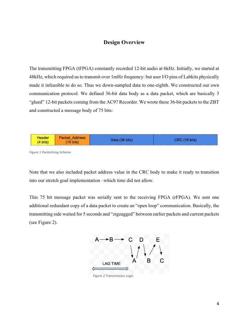
Design Overview
The transmitting FPGA (tFPGA) constantly recorded 12-bit audio at 6kHz. Initially, we started at
48kHz, which required us to transmit over 1mHz frequency: but user I/O pins of Labkits physically
made it infeasible to do so. Thus we down-sampled data to one-eighth. We constructed our own
communication protocol. We defined 36-bit data body as a data packet, which are basically 3
“glued” 12-bit packets coming from the AC97 Recorder. We wrote these 36-bit packets to the ZBT
and constructed a message body of 75 bits:
Figure1PacketizingScheme
Note that we also included packet address value in the CRC body to make it ready to transition
into our stretch goal implementation –which time did not allow.
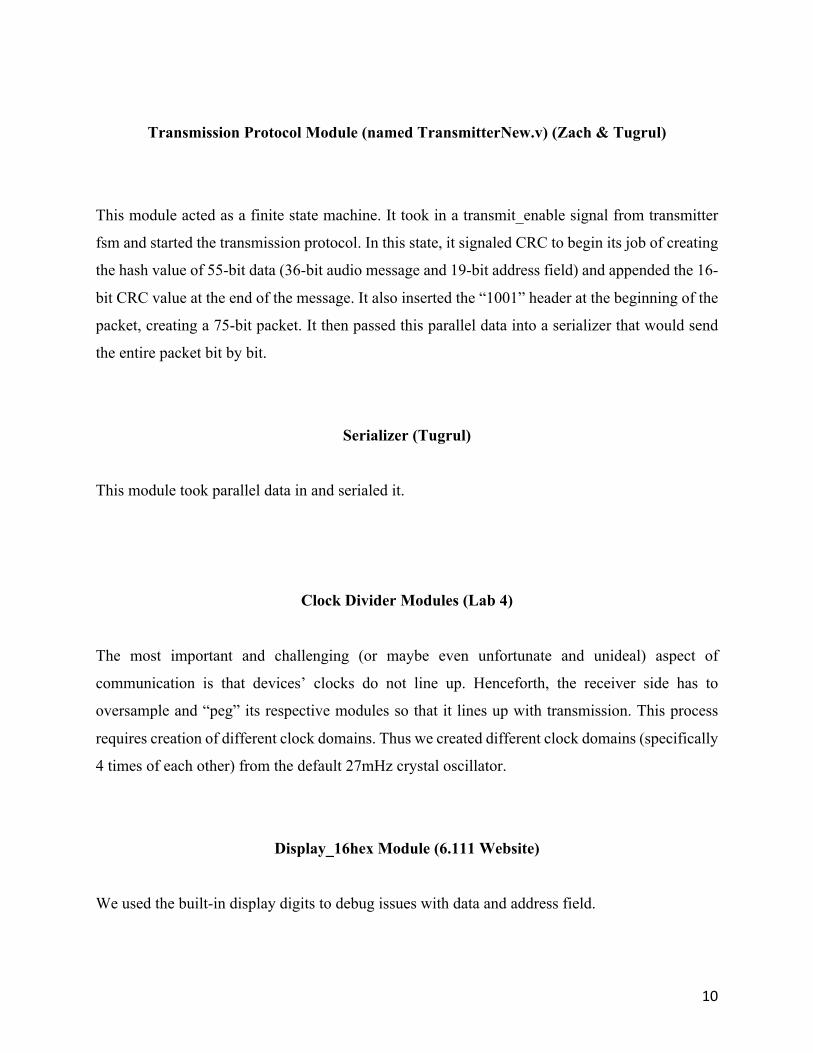
This 75 bit message packet was serially sent to the receiving FPGA (rFPGA). We sent one
additional redundant copy of a data packet to create an “open loop” communication. Basically, the
transmitting side waited for 5 seconds and “zigzagged” between earlier packets and current packets
(see Figure 2).
Figure2TransmissionLogic

5
The receiving FPGA checked the validity of an incoming packet by the header bits, resolved the
clock-domain differences between the transmitter FPGA (most challenging part of the project
indeed), ran the data through a CRC module and stored the data in a Block RAM memory. It
then played back audio after lag time has passed.
Below is the high level block diagram of our digital logic that contains a subset of our modules.
Description of all modules can be found at the next section.
High-Level Block Diagram

6
Hardware
In addition to two 6.111 Labkits, we initially utilized a pair of AV02 Fiber Optic Transmitter and
Receiver. We integrated them into the protoboard and interfaced them with the labkits as
follows:
Transmitter Circuit Receiver Circuit
It turns out digital abstraction is not really an absolute abstraction!
While fiber optic circuit worked just fine during the unit testing (since we tested it with lower
frequencies), it proved to be infeasible during the end to end project testing close to the end of
the project deadline. The ringing phenomena caused significant (65%) signal integrity casualties.
Thus, due to timing constraints we switched to using a physical wire between two FPGAs instead
of focusing on changing AV02 circuit elements.

7
Implementation and Modules
Synthesizing all the subproblems of the project was done using Verilog modules. Each of our
labkits had its respective copy of modules.
The modules below are topologically sorted in terms of order of function.
TRANSMITTING SIDE
AC97 Recorder and Playback Modules (Zach)
AC97 Recorder: This is the analog-to-digital converter that allowed us to sample the incoming
audio signal from a microphone through line-in. This was implemented in the AC97 module, but
we modified our existing audio lab to sample at 6kHz (formerly 48kHz) and at a bit depth of 12
bits. This allowed values from -2048 to 2047 using a 12-bit signed data bus. The module also
output to the high level FSM of transmitter that guided store the data in ZBT memory.

8
Memory (Zach)
ZBT Memory: This was the storage center for the FPGA that housed our audio data. With two
banks of 512kb x 36 bit memory, we were able to store a maximum of 32 seconds of 6kHz 12-bit
audio per bank, more than enough to satisfy the 5 second lag. A ram clock module was also
implemented (that is not shown) to satisfy timing constraints of the ZBT memory block. Reading
and writing was done on separate cycles. To the receiver FPGA, we sent the data (of course) and
the address the data resided in.
Cyclic Redundancy Check Module (LPset6)
To determine whether or not we have successfully transmitted a packet of data to the rFPGA, we
had a cyclic redundancy check module which that output a data integrity signal to the FSM. If the
packet is intact, we sent a PACKET_OK signal and then the packet itself was loaded into BRAM.
If the CRC failed, we send a PACKET_ERROR signal did not write the packet to the bram.

9
Transmitting FSM (Zach)
Transmitting FSM conducts the behavior of transmitting side. Its crucial feature was to manage
the transmission of lagged, redundant copies. This module will determine if we are currently
sampling information from the AC97 module and writing to memory. It muxed between the
AC_97 address and lagged address (when 5-second lag time passed). Essentially, it helped ensure
we routed data in the right direction. Its transmission logic is visualized below (Figure 2
reproduced)
Parallelizer (Tugrul)
This module took serial data in and deserialed it to a parallel state.
Figure3TransmissionLogic
10
Transmission Protocol Module (named TransmitterNew.v) (Zach & Tugrul)
This module acted as a finite state machine. It took in a transmit_enable signal from transmitter
fsm and started the transmission protocol. In this state, it signaled CRC to begin its job of creating
the hash value of 55-bit data (36-bit audio message and 19-bit address field) and appended the 16-
bit CRC value at the end of the message. It also inserted the “1001” header at the beginning of the
packet, creating a 75-bit packet. It then passed this parallel data into a serializer that would send
the entire packet bit by bit.
Serializer (Tugrul)
This module took parallel data in and serialed it.
Clock Divider Modules (Lab 4)
The most important and challenging (or maybe even unfortunate and unideal) aspect of
communication is that devices’ clocks do not line up. Henceforth, the receiver side has to
oversample and “peg” its respective modules so that it lines up with transmission. This process
requires creation of different clock domains. Thus we created different clock domains (specifically
4 times of each other) from the default 27mHz crystal oscillator.
Display_16hex Module (6.111 Website)
We used the built-in display digits to debug issues with data and address field.

11
RECEIVING SIDE
Checkpoint Module (probably the most complex module) (Tugrul & Zach)
Checkpoint module is a finite state machine that transitioned into a triggered stage whenever it
received a high bit (1). It then transitioned into a checker state where it expected a subsequent
“001” to complete a valid header of “1001.” In that case, it triggered the CRC check and started
the receival protocol. This module was then augmented by Zach to do a very crucial job:
oversample the data and meanwhile peg a “receiving clock” that successfully aligns with
transmission and drives the rest of the modules.
Receiver Finite State Machine (named receiverNew) (Tugrul)
This module conducts the safe and sound routing of data throughout the receiving device. It takes
in crc condition signals (crc_done and crc_good) and depacketizes the data accordingly.
Specifically, it splices the data packet into the address field, which then is used as an input to the
BRAM memory, and the audio message itself. It tells the bram memory module to write the packet
into the specified address by a write_enable signal.

12
Block Ram Memory (Tugrul)
We wrote the incoming data into a block ram that had 2^16 logs and 36 bit width, just enough to
handle around ten seconds of data. The data stored in this memory was then passed into the
AC97 playback module that played the data.
AC97 Playback: The digital-to-analog converter that converted our internal digitized and
packetized audio signal from memory to an analog signal to be used by the receiver module. The
input is a 36-bit bus. This bus was depacketized into three 12-bit buses. Its output was a single
wire out, again handled by the ac97 module.

13
Modifications from Original Proposal
Our instructor Dr. Gim Hom suggested that we make the feedback infrastructure a stretch goal
rather than the goal. For the goal, we were recommended that we take on an Open Loop
transmission –that we send redundant copies of a message with a lag. As the entire paper suggests
until this very page, we took on this advice. Apart from this change, we almost sticked identical to
our proposal in terms of timeline and responsibilities.
However, while we’ve come to appreciate the challenges of communication, we discovered many,
many setbacks along the way. Below are two setbacks, their detailed descriptions and the
approaches we took.
Visible Light Communication to Visible Wire Communication
Our initial motivation in starting our project was an ambition to get exposed to how communication
was done between two devices and to utilize visible light technology to make it more interesting
and fun. We succeeded in utilizing the fiber optic receiver/transmitter circuitry shown in the
hardware section. However, the circuitry did not respond well to higher frequencies which we did
not detect in the earlier stages of the project. While doing an end to end testing, we figured serious
signal integrity issues with frequencies higher than 50kHz. Due to the stage we were at, at that
time, we did not delve into debugging the ringing phenomena and switched to a single, physical
wire between the 2 FPGAs. In another view, it is easy to argue that the fiber optic circuitry basically
acts like a “fancy” wire. Actually, our “fancy” wire came really into handy as a debugging tool:
we were able to slow the clock frequencies down to Hz ranges and actually able to see when a bit
14
was being transmitted. It was indeed amazing to see how a packet (such as “DEADBEEF1”) could
successfully be seen on the other FPGA.
Thus, we continued the high frequency transmission with a physical wire and sometimes did the
debugging with the fiber optic circuitry driven by small clock frequencies. In the end, we were
content about the decision since the main point of the project was exposure to communication
methods, handling interruption and not mainly the visible light aspect.
High-Frequency Limitation of Labkit User IO pins: 48kHz to 6kHz Sampling
We discovered that Labkit IO pins could not drive faster than 1 mHz. Thus, we down-sampled
our data to 1/8 to provide a leeway for slower transmission. This way we slowed transmission
rate down to 480kbps. Down-sampling also caused a reduction in audio quality received.

15
What Went Wrong
After the abovementioned approaches were taken, we still ended up with a bug remaining in the
entire integration.
The expectation: System correctly transmits and receives message. When communication
between two labkits was interrupted, we desired to hear the message without interruption. We
should hear nothing once the lag-time tolerance was achieved.
The final outcome with the bug: System correctly transmitted and received data. When wire was
unplugged, we heard the message without interruption. However, we heard repetitions of the
last 5 seconds. In other words, instead of audio halting, it looped the last 5 seconds until we
replugged the wire. Communication resumed normally when wire was plugged back in (as
expected!)

16
Discussion and Conclusion
6.111 Visible Light Communication was indeed a substantial exposure to what we wanted:
communication. We had to reinvent the wheel every single time we wanted to implement a module.
We wrote our communication protocols, we learnt how to write to and read from memory
efficiently, we learnt how to interface new elements with our labkits and took a great risk of
working with something that we never did before.
We believe each of us has indeed lived through the legendary “Digital Death” experience.
Lamenting on even half a second signal delay (e.g. phone, internet etc) in our daily lives, we both
now highly respect and appreciate what communication infrastructure harbors within and how
complex it can be.
In addition, we learnt significant aspects that deserve to be shown on bold below:
Digital abstraction is not really an absolute abstraction!
The ringing effects caused by the fiber optic circuit and the user IO pins’ frequency are the best
examples. In other words, we learnt that whenever there is an analog system connected to a
digital system, analog system becomes the bottleneck. It was rather time consuming yet
rewarding to experience that analog and digital systems do not work mutually exclusively.
Things need not work in real world as they do in utopic testbenches!
I am a CS-oriented 6-2 student, and this has been a life-changing lesson for me. In software, code
is not generally interfaced with the real world. If code works in tests, it’ll work anywhere.
However, by definition, Verilog describes hardware that works with the physical world.

17
Thus many times we were faced with situations where code worked perfectly in testbenches but
not in the labkit (e.g. 1mHz limitation).
You never know the complexity until you work with it.
When we were suggested to use the open loop infrastructure for the main goal and not the
feedback infrastructure, we both thought it would be almost trivial to implement. However we
ended up encountering problems one over the other and spent many, many hours at the lab from
day 1. We even ended up with a bug in our final project state!
In conclusion, we strived to engineer a communication infrastructure that is robust to an
interference up to a certain limit. Through this demanding experience, we learnt how to think
better about communication, were required to reinvent some wheels (and debug/polish these
wheels!), had a great exposure to protocols, and achieved a great vision of trade-offs in real
systems: speed and memory. In big picture, our project taught us how to approach digital
systems, augmented with a firm teamwork.