netserver.aip.orgnetserver.aip.org/.../E-APPLAB-107-031532/APL_supp_0728.docx · Web...
16
Supplementary Material Cycling Excitation Process: An Ultra Efficient and Quiet Signal Amplification Mechanism in Semiconductor Yu-Hsin Liu 1 , Lujiang Yan 2 , Alex Zhang 2 , David Hall 2 , Iftikhar Ahmad Niaz 2 , Yuchun Zhou 2 , L. J. Sham 3 , and Yu-Hwa Lo 1,2* 1 Materials Science and Engineering Program, University of California, San Diego, 9500 Gilman Drive, La Jolla, California 92093-0418, USA 2 Department of Electrical and Computer Engineering, University of California, San Diego, 9500 Gilman Drive, La Jolla, California 92093-0409, USA 3 Department of Physics, University of California, San Diego 9500 Gilman Drive, La Jolla, California 92093, USA * [email protected] 1. Device Fabrication The OMCVD sample was grown by an epitaxial vendor. The 650nm deep device mesa was formed by inductively coupled plasma reactive-ion etching (ICP-RIE) with C4F8 and SF6 gases. The device mesa has a light sensitive area of 35 by 55 micrometers. After the mesa etch, a 300 nm thick layer of SiO 2 was deposited and patterned lithographically to form n- and p-metal contacts. E-beam evaporated Ti/Au was used to form the n- and p-Ohmic contacts. The metal contact was annealed at 290°C for 40 seconds in a rapid thermal annealing chamber.
Transcript of netserver.aip.orgnetserver.aip.org/.../E-APPLAB-107-031532/APL_supp_0728.docx · Web...

Supplementary Material
Cycling Excitation Process: An Ultra Efficient and Quiet Signal Amplification Mechanism in Semiconductor
Yu-Hsin Liu1, Lujiang Yan2, Alex Zhang2, David Hall2, Iftikhar Ahmad Niaz2, Yuchun Zhou2, L. J. Sham3, and Yu-Hwa Lo1,2*
1 Materials Science and Engineering Program, University of California, San Diego, 9500 Gilman Drive, La Jolla, California 92093-0418, USA2 Department of Electrical and Computer Engineering, University of California, San Diego, 9500 Gilman Drive, La Jolla, California 92093-0409, USA3 Department of Physics, University of California, San Diego 9500 Gilman Drive, La Jolla, California 92093, USA* [email protected]
1. Device FabricationThe OMCVD sample was grown by an epitaxial vendor. The 650nm deep device mesa was
formed by inductively coupled plasma reactive-ion etching (ICP-RIE) with C4F8 and SF6 gases.
The device mesa has a light sensitive area of 35 by 55 micrometers. After the mesa etch, a 300
nm thick layer of SiO2 was deposited and patterned lithographically to form n- and p-metal
contacts. E-beam evaporated Ti/Au was used to form the n- and p-Ohmic contacts. The metal
contact was annealed at 290°C for 40 seconds in a rapid thermal annealing chamber.
2. Dynamic Analysis of CEP Devices Here we model the characteristics of the CEP junction by a set of rate equations, and calculate
the CEP gain under steady state. The model takes into account carrier excitation from impurity
states in the compensated region and the roles of phonons, including the critical phonon
absorption process required for the generation of new e-h pairs and the countering process of
phonon emission. At first, all symbols are defined and listed below.
pA: Concentration (cm−3 ) of “unoccupied” acceptors in the n-region.
nD: Concentration (cm−3 ) of “occupied” donors in the p-region.
ph: Concentration (cm−3 ) of holes in the valence band of the n-region.
ne: Concentration (cm−3 ) of electrons in conduction band of the p-region.
N A: Total acceptor concentration (cm−3 ) in the n-region.
N D: Total donor concentration (cm−3 ) in the p-region.
V n: Effective volume (cm3 ) in the n-region that contributes to the CEP effect.
V p: Effective volume (cm3 ) in the p-region that contributes to the CEP effect.
ΩX: Effective volume (cm3 ) of Coulomb interaction between an energetic electron and an
occupied acceptor.
ΩY : Effective volume (cm3 ) of Coulomb interaction between an energetic hole and an unoccupied
donor.
τ : Single path carrier transit time ( sec ) across the depletion region.
τ h: Phonon absorption time ( sec ) for an unoccupied acceptor in the n-region to absorb a phonon
to produce a hole in the valence band.
τ n: Phonon absorption time ( sec ) for an occupied donor in the p-region to absorb a phonon to
produce an electron in the conduction band.
W e: Phonon emission coefficient (cm3/ s) between electrons and the unoccupied donors in the p-
region.
W h : Phonon emission coefficient (cm3/ s) between holes and the occupied acceptors in the n-
region.
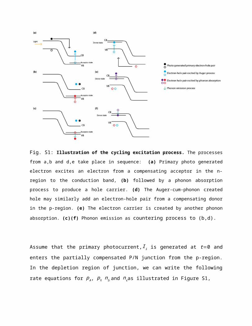
Fig. S1: Illustration of the cycling excitation process. The processes from a,b and d,e take place in
sequence: (a) Primary photo generated electron excites an electron from a compensating acceptor in the
n-region to the conduction band, (b) followed by a phonon absorption process to produce a hole carrier.
(d) The Auger-cum-phonon created hole may similarly add an electron-hole pair from a compensating
donor in the p-region. (e) The electron carrier is created by another phonon absorption. (c)(f) Phonon
emission as countering process to (b,d).
Assume that the primary photocurrent,I i is generated at t=0 and enters the partially compensated
P/N junction from the p-region. In the depletion region of junction, we can write the following
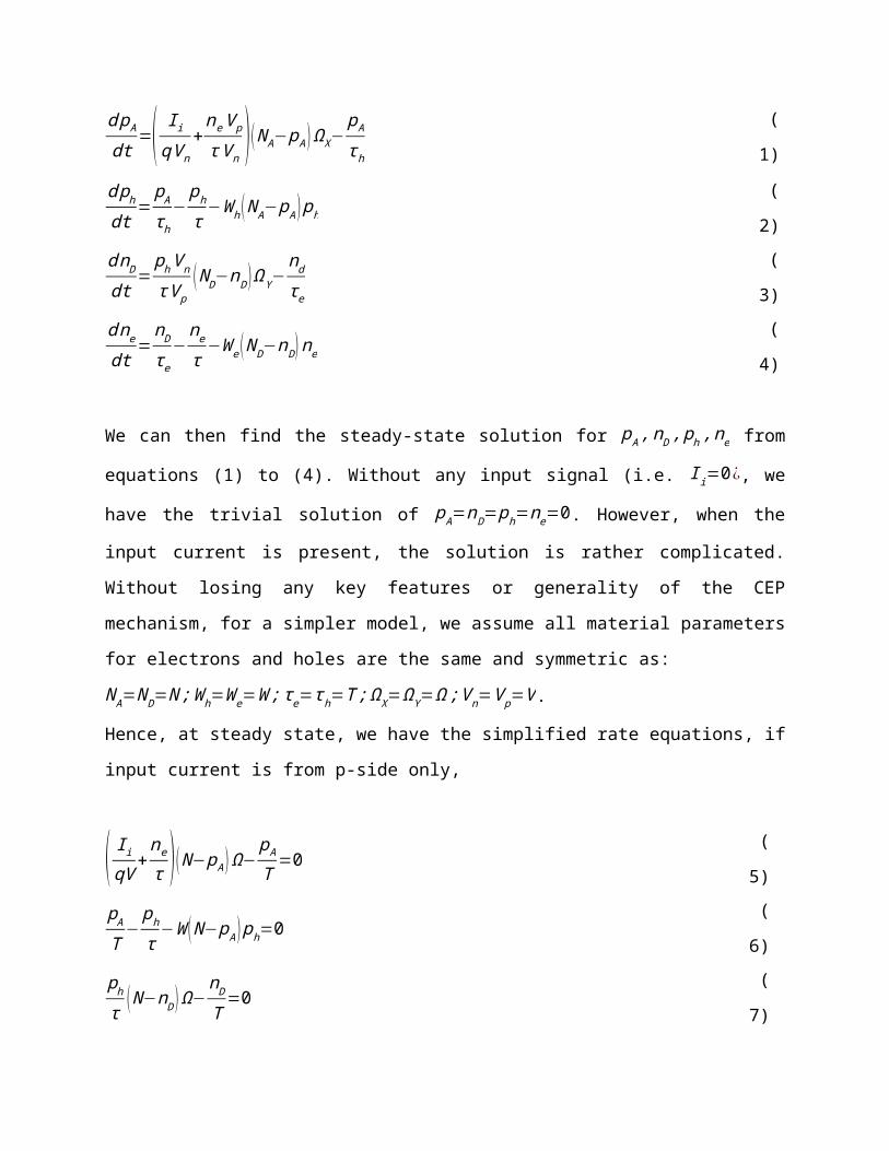
rate equations for pA, ph nD, and neas illustrated in Figure S1,
d pA
dt=( I i
qV n+
ne V p
τ V n) ( N A−pA ) ΩX−
pA
τh(1)
d ph
dt=
pA
τh−
ph
τ−W h ( N A−pA ) ph (2)
d nD
dt=
ph V n
τ V p( N D−nD ) ΩY−
nd
τ e(3)
d ne
dt=
nD
τ e−
ne
τ−W e ( N D−nD ) ne (4)
We can then find the steady-state solution for pA , nD , ph , ne from equations (1) to (4). Without
any input signal (i.e. I i=0 ¿, we have the trivial solution of pA=nD=ph=ne=0. However, when
the input current is present, the solution is rather complicated. Without losing any key features or
generality of the CEP mechanism, for a simpler model, we assume all material parameters for
electrons and holes are the same and symmetric as:
N A=N D=N ;W h=W e=W ;τe=τh=T ;ΩX=ΩY=Ω ;V n=V p=V .
Hence, at steady state, we have the simplified rate equations, if input current is from p-side only,
( Ii
qV+
ne
τ ) ( N−p A ) Ω−pA
T=0 (5)
p A
T−
ph
τ−W ( N−pA ) ph=0 (6)
ph
τ ( N−nD ) Ω−nD
T=0 (7)
nD
T−
ne
τ−W ( N−nD ) ne=0 (8)
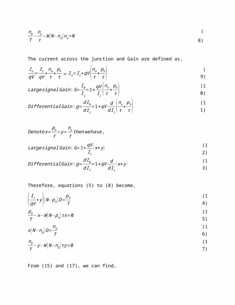
The current across the junction and Gain are defined as,
I o
qV=
I i
qV+
ne
τ+
ph
τ⇔ I o=I i+qV ( ne
τ+
ph
τ ) (9)
Large signalGain :G=I 0
I i=1+ qV
I i( ne
τ+
ph
τ ) (10)
Differential Gain :g=d I 0
d I i=1+qV d
d I i( ne
τ+
ph
τ ) (11)
Denote x=ph
τ∧ y=
ne
τthen we have ,
Large signal Gain :G=1+ qVIi
( x+ y ) (12)
Differential Gain :g=d I 0
d I i=1+qV d
d I i( x+ y ) (13)
Therefore, equations (5) to (8) become,
( Ii
qV+ y) ( N−p A ) Ω=
pA
T(14)
p A
T−x−W ( N−p A ) τx=0 (15)
x ( N−nD ) Ω=nD
T(16)
nD
T− y−W ( N−nD ) τy=0 (17)
From (15) and (17), we can find,
pA=(1+WNτ ) Tx
1+WTτx(18)
nD=(1+WNτ ) Ty
1+WTτy(19)
Substitute (18) and (19) into (14) and (16). After some simplification, we have,
( Ii
qV+ y)(1− T
Nx)=1+WNτ
N Ωx (20)
x (1− TN
y )=1+WNτN Ω
y (21)
Denoteconstants : A=1+WNτN Ω
; B= TN
;C=I i
qV
With the new notation, equations (20) and (21) become,
(C+ y ) (1−Bx )=Ax (22)x (1−By )=Ay (23)
Solve (22) (23) for x and y,
x=1−A2 B
+√( A−12 B )
2
+ ACB (1+ A+BC )
(24)
y= 1−A−BC2 B
+√( A+BC−12 B )
2
+ C( A+1 ) B
(25)
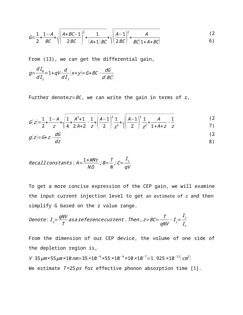
From (12), we can find the large signal gain as,
G=1+ qVIi
(x+ y )=1+ x+ yC
G=12+ 1−A
BC+√( A+BC−1
2BC )2
+ 1( A+1 ) BC
+√( A−12 BC )
2
+ ABC (1+ A+BC )
(26)
From (13), we can get the differential gain,
g=d I 0
d I i=1+qV d
d Ii( x+ y )=G+BC ∙ dG
d ( BC )
Further denotez=BC, we can write the gain in terms of z,
G ( z )=12+ 1−A
z+√ 1
4+ A2+1
2 A+2∙ 1
z+( A−1
2 )2 1
z2 +√( A−12 )
2 1z2 +
A1+ A+z
∙ 1z
(27)
g ( z )=G+z ∙ dGdz (28)
Recall constants : A=1+WNτN Ω
;B= TN
;C=I i
qV
To get a more concise expression of the CEP gain, we will examine the input current injection
level to get an estimate of z and then simplify G based on the z value range.
Denote : I s=qNV
Tas a referencecurrent . Then , z=BC= T
qNV∙ I i=
Ii
I s
From the dimension of our CEP device, the volume of one side of the depletion region is,
V 35 μm ×55 μm ×10 nm=35 ×10−4 ×55×10−4 ×10 ×10−7=1.925 ×10⁻¹¹ ( cm3 )
We estimate T ≈ 25 ps for effective phonon absorption time [1].
I s=qNV
T=1.602 ×10−19×2×1019 ×1.925 ×10−11
25× 10−12 =2.5 ( Amps ) (29)
This reference current value is huge compare to the current injection level in our measurements,
which is on the order of nano-ampere. Therefore, all the measurements were assumed to be done
under low current injection condition.

i .e . I i≪ I s⇒ z=I i
I s≪1
Re-arrange equation (27) also considering z≪1
G ( z )=12 +
1−Az +|A−1
2 ∙ 1z|√ 1
4 ∙( 2A−1 )
2
∙ z2+A2+1
2 A+2 ∙( 2A−1 )
2
∙ z+1+√1+( 2A−1 )
2
∙ A1+ A ∙ z
Denote , f ( z )=√ 14
∙( 2A−1 )
2
∙ z2+ A2+12 A+2
∙( 2A−1 )
2
∙ z+1+√1+( 2A−1 )
2
∙ A1+A
∙ z
G ( z )=12+ 1−A
z+|A−1
2∙ 1
z|∙ f ( z ) (30)
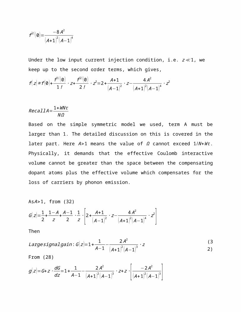
Apply Taylor series expansion on f ( z )
f ( z )=∑n=0
∞ f (n ) (0 )n!
zn=f ( 0 )+ f (1 ) (0 )1 !
∙ z+ f ( 2) (0 )2!
∙ z2+… (31)
f (0 )=2
f (1) (0 )= A+1( A−1 )2
f (2 ) (0 )= −8 A2
( A+1 )2 ( A−1 )4
Under the low input current injection condition, i.e. z≪1, we keep up to the second order terms,
which gives,
f ( z )≅ f (0 )+ f (1 ) (0 )1 !
∙ z+ f ( 2) (0 )2!
∙ z2=2+ A+1( A−1 )2
∙ z− 4 A2
( A+1 )2 ( A−1 )4∙ z2
Recall A=1+WNτN Ω
Based on the simple symmetric model we used, term A must be larger than 1. The detailed
discussion on this is covered in the later part. Here A>1 means the value of Ω cannot exceed
1/ N+Wτ . Physically, it demands that the effective Coulomb interactive volume cannot be
greater than the space between the compensating dopant atoms plus the effective volume which
compensates for the loss of carriers by phonon emission.
As A>1, from (32)
G ( z )=12+ 1−A
z+ A−1
2∙ 1
z∙[2+ A+1
( A−1 )2∙ z− 4 A2
( A+1 )2 ( A−1 )4 ∙ z2]Then
Large signal gain :G ( z )=1+ 1A−1
− 2 A2
( A+1 )2 ( A−1 )3∙ z (32)
From (28)
g ( z )=G+z ∙ dGdz
=1+ 1A−1
− 2 A2
( A+1 )2 ( A−1 )3∙ z+z ∙[ −2 A2
( A+1 )2 ( A−1 )3 ]Differential gain : g ( z )=1+ 1
A−1− 4 A2
( A+1 )2 ( A−1 )3∙ z (33)
Recall constants : A=1+WNτN Ω
;B= TN
;C=I i
qV; I s=
qNVT
∧z=BC=I i
I s
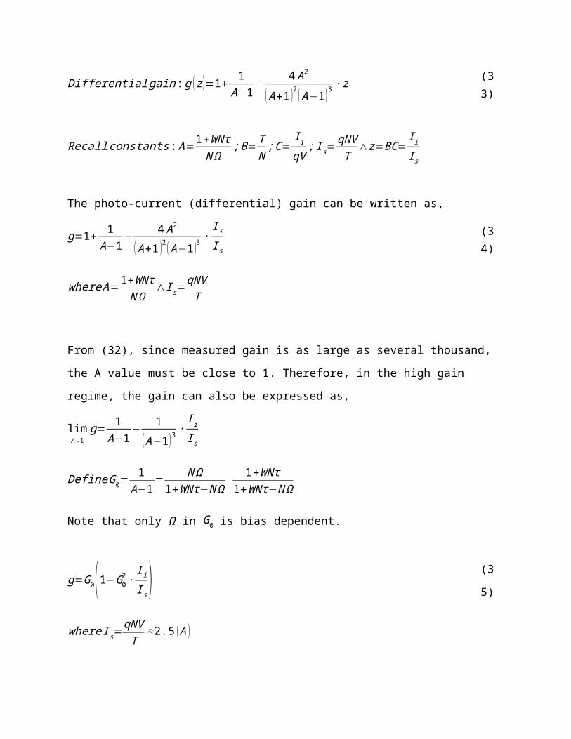
The photo-current (differential) gain can be written as,
g=1+ 1A−1
− 4 A2
( A+1 )2 ( A−1 )3∙I i
I s(34)
where A=1+WNτN Ω
∧I s=qNV
T
From (32), since measured gain is as large as several thousand, the A value must be close to 1.
Therefore, in the high gain regime, the gain can also be expressed as,
limA → 1
g= 1A−1
− 1( A−1 )3
∙Ii
I s
Define G0=1
A−1= N Ω
1+WNτ−N Ω1+WNτ
1+WNτ−N Ω

Note that only Ω in G0 is bias dependent.
g=G0(1−G02 ∙
Ii
I s) (35)
where I s=qNV
T≈ 2.5 ( A )
Equation (35) is the gain expression in the main text.
The maximum achievable gain can be found by settingdg
d Go=0, which gives the maximum gain
under a given input current,
Gmax2√3
9∙√ I s
I i
(36)
Estimate of the numerical value of WNτ
The term, WNτ in Go can be treated as the time ratio between carrier transmission through the depletion
region and carrier transition from the mobile bands to the localized compensating impurity states via
phonon emission.
From [2], the electron capture cross section,
σ=20|uf|
2
T×10−12 (cm2 ) where|u f|
2≈ 165
Using this result and approximate the thermal velocity of electrons by RMS value
⟨ v ⟩≅ √⟨ v2 ⟩=√ 3 kB Tm¿ =√ 3kB T
0.26 me
Therefore the electron capture / phonon emission coefficient @ room temperature is approximated by,
W =σ ⟨ v ⟩=20 ×10−12
65 ×300×√ 3 × 1.38× 10−23× 300
0.26 ×9.11× 10−31 ×102 (cm3/ s)≅ 2.4 × 10⁻⁸ (cm3/s )
For our device, N 2× 10¹⁹ ( cm−3 ) and the carrier transit time, τ, across the narrow (~20nm) depletion
region is around 0.1ps. Thus
WNτ 2.4 ×10−8× 2×1019×10−13=0.05≪1
The result indicates that phonon emission plays a relatively minor role for the CEP device. Therefore, in
the discussion of the main text we have omitted this effect for simplicity.
Discussions
Equation (34) shows analytically, after some approximations, several key features of the CEP
gain: (1) the dependence of the CEP gain on the input signal which is proportional to the light
intensity; (2) the relation between the achievable gain and the bias-dependent Coulomb
interaction between energetic carriers and the compensating ionized dopants represented through
the effective interaction volume Ω (cm3); (3) dependence of the CEP gain on the concentration of
compensating impurity and the phonon absorption time the latter of which we refer to as
“phonon bottleneck”. We describe each effect in more detail next.
1. Gain decrease with increasing input signal
From equation (34), the model predicts the decrease in gain with increasing current injection I i.
This characteristic has been experimentally observed as shown in Fig. S2 (also in Fig. 2 in the
main text). Within the range of primary photocurrent that has been measured, the gain decreases
almost linearly with the primary photocurrent (i.e. input signal to the CEP junction), as predicted
by equation (34). The different magnitude of gain under different bias in Fig. S2 is due to the
voltage dependence of the “A” coefficient to be explained next.
Fig. S2 (Fig. 2b): Input power (represented by the primary photocurrent under 635nm light at
zero bias) dependence of gain under different reverse bias.
2. Gain dependence on voltage bias
At a bias voltage as low as 3V, our measurement shows a maximum gain of several thousand in
Fig. S2. Correspondingly, the model shows when the only voltage dependent term “A” in
equation (34), approaches 1, the highest gain is reached. Under this condition, the effective
interaction volume of the impurity, Ω approaches the maximum value of1/ N+Wτ , signifying the
strongest achievable CEP effect.
This means the effective CEP volume Ω for the compensating impurity rises quickly with the
increasing bias and saturates at about ~3V. In such condition, every hot carrier “sees” the whole
volume of its path covered by the compensating impurity thus having the maximum chance to
excite new generation carriers. Furthermore, the additional term Wτ in Ω besides 1/ N
compensates for the loss of excited carriers due to recombination via phonon emission, which is
a relatively minor effect since phonon emission time (2.5ps) is usually much slower than the
carrier transit time across the CEP junction (~0.1 ps)1-2.
3. Gain increase with increasing temperature
With a higher temperature, the effective phonon absorption time, T, is reduced due to the Bose-
Einstein distribution of phonons. The current I s in equation (34) is equal to I s=qNV
T , so a longer
phonon absorption time causes a greater gain decrease with input current. In other words, for the
same input signal, the CEP device having a longer phonon absorption time shows a lower gain
according to our model. This is consistent with the observed gain decrease at lower temperature
as shown in Fig. S3.

Fig. S3 (Fig. 2c): Temperature dependence of gain under 635nm illumination. The gain values are normalized to the 300K gain at 3V reverse bias.
4. Gain saturation with increasing voltage
While increasing the voltage, the effective CEP volume quickly saturates to the value of1N
+Wτ
that produces the highest gain. The maximum achievable gain under a given input current is
Gmax2√3
9∙√ I s
I i
as derived in equation (36). Note that the maximum achievable CEP gain
decreases with increasing input current and the phonon absorption time, and increases with the
amount of compensating impurity. For a quick numerical estimation from equation (29), in our
device we have I s ≈ 2.5 ( Amps ) and have used input photocurrent of around I i≈ 1 (nA ), the above
equation suggests a maximum gain of around 20,000, which is of the same order as our measured
value in Fig. S2.
Reference1. T. R. Hart, R. L. Aggarwal and B. Lax, Phys. Rev. B. 1, 638 (1970).
2. H. Gummel and M. Lax. Annals of Physics. 2.1, 28-56 (1957).