VIBRATION SUPPRESSION OF ROTATING BEAMS THROUGH ...
103
VIBRATION SUPPRESSION OF ROTATING BEAMS THROUGH PIEZOELECTRIC SHUNT CIRCUITS by PRESTON POWELL JINWEI SHEN, COMMITTEE CHAIR WEIHUA SU STEVE SHEPARD HAO KANG A THESIS Submitted in partial fulfillment of the requirements for the degree of Master of Science in the Department of Aerospace Engineering and Mechanics in the Graduate School of The University of Alabama TUSCALOOSA, ALABAMA 2016
Transcript of VIBRATION SUPPRESSION OF ROTATING BEAMS THROUGH ...
VIBRATION SUPPRESSION OF ROTATING
BEAMS THROUGH PIEZOELECTRIC
SHUNT CIRCUITS
by
PRESTON POWELL
JINWEI SHEN, COMMITTEE CHAIRWEIHUA SU
STEVE SHEPARDHAO KANG
A THESIS
Submitted in partial fulfillment of the requirementsfor the degree of Master of Science
in the Department of Aerospace Engineering and Mechanicsin the Graduate School of
The University of Alabama
TUSCALOOSA, ALABAMA
2016

Copyright Preston Powell 2016ALL RIGHTS RESERVED
ABSTRACT
This thesis analytically investigates the feasibility of passive vibration damping of a rotat-
ing beam-like structure, such as a helicopter rotor, through the use of piezoelectric materials.
Piezoelectric materials are unique, in that, they produce an electrical charge under the pres-
ence of mechanical stresses. Conversely, they generate mechanical stresses under applied
electrical loads. When mounted to a structure undergoing bending stresses, such as a can-
tilever beam, there is an exchange of mechanical and electrical energy between the beam
and the piezoelectric material. This electrical energy can be used to power small electronics
such as onboard data transmitters. This energy can also be dissipated through electrical
shunt circuits rather than being harvested for external use. Electrical components in a
shunt circuit (resistors, capacitors, and inductors) release energy from the system as Joule
heat. Energy dissipation corresponds to a vibration damping effect in the electromechanical
system. Numerous configurations of electrical components and mechanical structures are ex-
plored. First, the Rayleigh-Ritz method of assumed modes is adopted for a rotating uniform
single degree-of-freedom cantilever beam. Both in-plane (lag) and out-of-plane (flap) bend-
ing directions are considered. The beam model is modified to include piezoelectric elements
and electrical shunt circuits. Two types of shunt circuits are considered: one with a single
resistive element and one with a resistor and inductor in series. Various resistances are used
in finding the frequency and impulse responses of the rotating beam with a shunt circuit.
The change in damping potential between resistors is evaluated for each electromechanical
ii
system. The effects of the number of modes assumed when modeling the beam are also
highlighted. Single-mode approximations are found to be helpful in understanding the foun-
dations of the physics in the beam/piezo systems. It is also determined that multiple-mode
approximations account for important electromechanical behavior that is neglected by the
single-mode formulations. The settling times of the impulse responses are used as the figure
of merit to assess energy dissipation in the systems. Successful vibration damping of rotating
cantilever beams is predicted through the piezoelectric shunt circuits.
iii
NOMENCLATURE
b width
βi roots of characteristic equation for mode shapes
c modulus of elasticity
Ci mode shape coefficients
Cp piezoelectric capacitance
D electric displacement
d31 piezoelectric constant
e piezoelectric coupling coefficient
E electric field
ε dielectric constant
f external force
floc location of applied force
FT centrifugal force
g31 voltage coefficient
I current
K stiffness matrix
k31 coupling coefficient
iv

L inductance
m mass per unit length
M mass matrix
N number of modes
Ω rotational speed
ωe electrical frequency
φ electric potential location
Ψi mode shapes
q electrical charge
R beam length, resistance
r spatial coordinate along axis of beam
ρ density
S strain
t thickness
T stress, kinetic energy
Θ electromechanical coupling matrix
U potential energy
V volume
v
v lag displacement
Vi temporal lag displacement coordinate
v voltage
w flap displacement
Wi temporal flap displacement coordinate
We electrical energy
W work
Superscripts
E parameter at constant electrical field
S parameter at constant strain
T parameter at constant stress
( )′ first derivative with respect to spatial coordinate
( )′′ second derivative with respect to spatial coordinate
˙( ) first derivative with respect to time
( ) second derivative with respect to time
Subscripts
b beam parameter
vi
p piezoelectric parameter
sh shunt parameter
v pertains to lag bending motion
w pertains to flap bending motion
vii
ACKNOWLEDGMENTS
I wish to thank my advisor and committee chair, Dr. Jinwei Shen, for providing the
opportunity to work on this project. His patience and guidance were essential in the comple-
tion of this thesis. His door was always open for my frequent visits and questions, which he
always welcomed even during his busy schedule. He challenged and motivated me to work
my hardest when I got stuck or lost focus.
I want to acknowledge the resources and experiences provided by the Army Research
Laboratory in Aberdeen Proving Ground, Maryland. I would like to thank Dr. Hao Kang
specifically for his mentorship during my time at ARL. His support and research interests led
to the development of my thesis topic. He served on my committee and also gave valuable
input throughout the course of my research.
I would like to show my gratitude towards the other committee members, Dr. Weihua Su
and Dr. Steve Shepard. I recognize that their participation in this work took time from their
daily schedules. Their contributions and advice were helpful and their friendly personalities
made this process significantly less intimidating.
Additionally, I have a sincere appreciation for The University of Alabama and the De-
partment of Aerospace Engineering & Mechanics. The faculty and staff have all contributed
to my education and, for that, I am truly indebted. I am grateful for all of my friends and
fellow graduate students who helped me relax at times when I was most stressed. Their
input and encouragement throughout the past two years was crucial in not only maintaining
viii

my focus and drive, but also reminding me to take it easy sometimes.
Finally, I want to thank my family for their constant support since the day I was born.
Mom, Dad, Lindsay, and Ashlyn, you each have had an immeasurable influence on my life.
Your being a role model and showing me the importance of hard work and education has
given me continual motivation and is the reason I am where I am today.
ix
CONTENTS
ABSTRACT . . . . . . . . . . . . . . . . . . . . . . . . . . . . . . . . . . . . . . . . ii
NOMENCLATURE . . . . . . . . . . . . . . . . . . . . . . . . . . . . . . . . . . . . iv
ACKNOWLEDGMENTS . . . . . . . . . . . . . . . . . . . . . . . . . . . . . . . . . viii
LIST OF TABLES . . . . . . . . . . . . . . . . . . . . . . . . . . . . . . . . . . . . . xiii
LIST OF FIGURES . . . . . . . . . . . . . . . . . . . . . . . . . . . . . . . . . . . . xiv
1 INTRODUCTION . . . . . . . . . . . . . . . . . . . . . . . . . . . . . . . . . . . 1
1.1 MOTIVATION . . . . . . . . . . . . . . . . . . . . . . . . . . . . . . . . . . 1
1.2 PIEZOELECTRICITY . . . . . . . . . . . . . . . . . . . . . . . . . . . . . . 2
2 LITERATURE REVIEW . . . . . . . . . . . . . . . . . . . . . . . . . . . . . . . 6
2.1 ACTIVE CONSTRAINED LAYER DAMPING . . . . . . . . . . . . . . . . 6
2.2 ENERGY HARVESTING . . . . . . . . . . . . . . . . . . . . . . . . . . . . 8
2.3 SHUNT CIRCUITS . . . . . . . . . . . . . . . . . . . . . . . . . . . . . . . . 9
3 APPROACH . . . . . . . . . . . . . . . . . . . . . . . . . . . . . . . . . . . . . . 14
3.1 MATHEMATICAL MODEL . . . . . . . . . . . . . . . . . . . . . . . . . . . 17
3.2 RESISTIVE SHUNT CIRCUIT . . . . . . . . . . . . . . . . . . . . . . . . . 27
3.3 RESISTIVE-INDUCTIVE SHUNT CIRCUIT . . . . . . . . . . . . . . . . . 30
4 VERIFICATION AND RESULTS . . . . . . . . . . . . . . . . . . . . . . . . . . 36
x
4.1 NON-ROTATING BEAM VERIFICATION . . . . . . . . . . . . . . . . . . 36
4.2 ROTATING BEAM SINGLE MODE VERIFICATION . . . . . . . . . . . . 40
4.3 SINGLE MODE WITH R - SHUNT . . . . . . . . . . . . . . . . . . . . . . 44
4.3.1 FLAP BENDING . . . . . . . . . . . . . . . . . . . . . . . . . . . . . 44
4.3.2 LAG BENDING . . . . . . . . . . . . . . . . . . . . . . . . . . . . . 45
4.4 SINGLE MODE WITH RL - SHUNT . . . . . . . . . . . . . . . . . . . . . . 48
4.4.1 FLAP BENDING . . . . . . . . . . . . . . . . . . . . . . . . . . . . . 49
4.4.2 LAG BENDING . . . . . . . . . . . . . . . . . . . . . . . . . . . . . 50
4.5 ROTATING BEAM MULTIPLE MODES VERIFICATION . . . . . . . . . 52
4.6 MULTIPLE MODES WITH R-SHUNT . . . . . . . . . . . . . . . . . . . . . 56
4.6.1 FLAP BENDING . . . . . . . . . . . . . . . . . . . . . . . . . . . . . 56
4.6.2 LAG BENDING . . . . . . . . . . . . . . . . . . . . . . . . . . . . . 58
4.7 MULTIPLE MODES WITH RL-SHUNT . . . . . . . . . . . . . . . . . . . . 61
4.7.1 FLAP BENDING TUNED TO FIRST MODE . . . . . . . . . . . . . 61
4.7.2 FLAP BENDING TUNED TO SECOND MODE . . . . . . . . . . . 64
4.7.3 LAG BENDING TUNED TO FIRST MODE . . . . . . . . . . . . . 67
4.7.4 LAG BENDING TUNED TO SECOND MODE . . . . . . . . . . . . 69
5 DISCUSSION . . . . . . . . . . . . . . . . . . . . . . . . . . . . . . . . . . . . . 74
xi
5.1 SUMMARY OF RESULTS . . . . . . . . . . . . . . . . . . . . . . . . . . . . 74
5.2 DISCUSSION OF SHUNT SYSTEMS . . . . . . . . . . . . . . . . . . . . . 75
6 CONCLUSION . . . . . . . . . . . . . . . . . . . . . . . . . . . . . . . . . . . . . 80
6.1 DAMPING POTENTIAL . . . . . . . . . . . . . . . . . . . . . . . . . . . . 80
6.2 APPLICATION TO HELICOPTER ROTORS . . . . . . . . . . . . . . . . . 81
6.3 FUTURE WORK . . . . . . . . . . . . . . . . . . . . . . . . . . . . . . . . . 82
REFERENCES . . . . . . . . . . . . . . . . . . . . . . . . . . . . . . . . . . . . . . 84
xii
LIST OF TABLES
3.1 Equivalent Mechanical and Electrical Components in Equations of Motion . 33
4.1 Beam and PZT Physical Properties . . . . . . . . . . . . . . . . . . . . . . . 37
4.2 Piezoelectric Parameters of PZT-5H . . . . . . . . . . . . . . . . . . . . . . . 37
4.3 Curve Numbers in Figure 4.2 and Their Corresponding Resistor Values . . . 38
4.4 Beam and PZT Material Properties . . . . . . . . . . . . . . . . . . . . . . . 40
4.5 Simulation Parameters . . . . . . . . . . . . . . . . . . . . . . . . . . . . . . 41
4.6 Hart-II Blade Frequencies vs. Model Predicted Frequencies . . . . . . . . . . 43
4.7 Hart-II Blade Frequencies vs. Model Predicted Frequencies . . . . . . . . . . 55
5.1 Summary of Shunt Circuit Resistances and Settling Times for Impulse Re-
sponses of Flap and Lag Bending . . . . . . . . . . . . . . . . . . . . . . . . 75
xiii
LIST OF FIGURES
1.1 Dipole Alignment Before, During, and After Poling Process for Piezoelectric
Manufacturing . . . . . . . . . . . . . . . . . . . . . . . . . . . . . . . . . . . 4
2.1 ACLD sandwich configuration [1] . . . . . . . . . . . . . . . . . . . . . . . . 6
2.2 ACLD with sensor and controller [2] . . . . . . . . . . . . . . . . . . . . . . 7
2.3 Piezoelectric bimorph cantilever beam with tip mass [3] . . . . . . . . . . . . 8
2.4 Cantilever Beam with Driving and Shunted Piezoceramic Pairs [4] . . . . . . 10
2.5 Schematic of Energy Transfer in a Piezoelectric Shunt Circuit [5] . . . . . . . 10
2.6 Piezoelectric element connected to series RL-shunt [6] . . . . . . . . . . . . . 11
2.7 Cantilever Beam With Piezoelectric Elements Connected to Series and Parallel
RL-shunts [7] . . . . . . . . . . . . . . . . . . . . . . . . . . . . . . . . . . . 12
3.1 Schematic of a Rotating Cantilever Beam Undergoing Flap Bending . . . . . 15
3.2 Schematic of a Rotating Cantilever Beam Undergoing Lag Bending . . . . . 15
3.3 Dimensional Parameters for Beam/Piezo System Undergoing Flap Bending . 16
3.4 Dimensional Parameters for Beam/Piezo System Undergoing Lag Bending . 16
3.5 Beam/Piezo Schematic with Resistive Shunt Circuit for Flap and Lag Bending 28
3.6 R-Shunt Circuit Design . . . . . . . . . . . . . . . . . . . . . . . . . . . . . . 28
3.7 RL-Shunt Circuit Designs: Series vs. Parallel . . . . . . . . . . . . . . . . . . 31
xiv
3.8 Beam/Piezo Schematic with Resistive-Inductive Shunt Circuit for Flap and
Lag Bending . . . . . . . . . . . . . . . . . . . . . . . . . . . . . . . . . . . . 31
3.9 RL-Shunt Circuit Design . . . . . . . . . . . . . . . . . . . . . . . . . . . . . 32
4.1 Schematic of Cantilever Beam with Collocated Piezoelectric Elements Con-
nected to a Series RL-Shunt . . . . . . . . . . . . . . . . . . . . . . . . . . . 37
4.2 Transfer Response of Series RL-Shunt [7] . . . . . . . . . . . . . . . . . . . . 38
4.3 Transfer Response of Series RL-Shunt . . . . . . . . . . . . . . . . . . . . . . 39
4.4 Impulse Response of Tip Displacement for Rotating Beam/Piezo System With-
out Shunt: Flap vs. Lag . . . . . . . . . . . . . . . . . . . . . . . . . . . . . 42
4.5 Frequency Response of Rotating Beam/Piezo System Without Shunt: Flap
vs. Lag . . . . . . . . . . . . . . . . . . . . . . . . . . . . . . . . . . . . . . . 43
4.6 Flap Bending Frequency Response of R-Shunt System for Various Resistor
Values . . . . . . . . . . . . . . . . . . . . . . . . . . . . . . . . . . . . . . . 44
4.7 Flap Bending Impulse Response of Tip Displacement: R-Shunt vs. No Shunt 45
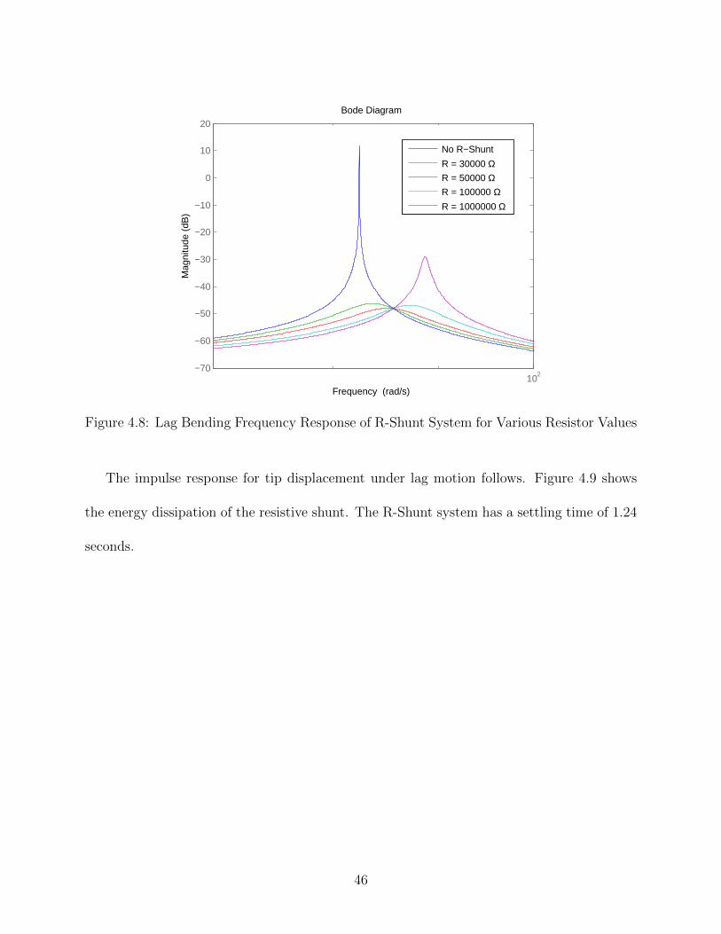
4.8 Lag Bending Frequency Response of R-Shunt System for Various Resistor Values 46
4.9 Lag Bending Impulse Response of Tip Displacement: R-Shunt vs. No Shunt 47
4.10 Impulse Response of Tip Displacement for System with 30000 Ω R-Shunt:
Flap vs. Lag . . . . . . . . . . . . . . . . . . . . . . . . . . . . . . . . . . . . 48
4.11 Flap Bending Frequency Response of RL-Shunt System for Various Resistor
Values . . . . . . . . . . . . . . . . . . . . . . . . . . . . . . . . . . . . . . . 49
xv
4.12 Flap Bending Impulse Response of Tip Displacement: R-Shunt vs. No Shunt 50
4.13 Lag Bending Frequency Response of RL-Shunt System for Various Resistor
Values . . . . . . . . . . . . . . . . . . . . . . . . . . . . . . . . . . . . . . . 51
4.14 Lag Bending Impulse Response of Tip Displacement: R-Shunt vs. No Shunt 52
4.15 Flap Bending Impulse Response of Beam/Piezo System (N=3) . . . . . . . . 53
4.16 Lag Bending Impulse Response of Beam/Piezo System (N=3) . . . . . . . . 54
4.17 Multiple Mode Frequency Response of Beam/Piezo System: Flap vs. Lag . . 55
4.18 Flap Bending Frequency Response at Resonant Frequencies For Various Re-
sistor Values . . . . . . . . . . . . . . . . . . . . . . . . . . . . . . . . . . . . 57
4.19 Flap Bending Impulse Response of R-Shunt System With 30000 Ω and 15000
Ω Resistors . . . . . . . . . . . . . . . . . . . . . . . . . . . . . . . . . . . . 58
4.20 Lag Bending Frequency Response at Resonant Frequencies For Various Resis-
tor Values . . . . . . . . . . . . . . . . . . . . . . . . . . . . . . . . . . . . . 59
4.21 Lag Bending Impulse Response of R-Shunt System With 50000 Ω, 10000 Ω,
and 5000 Ω Resistors . . . . . . . . . . . . . . . . . . . . . . . . . . . . . . . 60
4.22 Flap Bending Frequency Responses of RL-Shunt System for Various Resistors 62
4.23 Flap Bending Impulse Response with RL-Shunt and 25000 Ω Resistor . . . . 63
4.24 Flap Bending Impulse Response with RL-Shunt and 120000 Ω Resistor . . . 64
4.25 Flap Bending Frequency Responses of RL-Shunt System for Various Resistors 66
xvi
4.26 Flap Bending Impulse Response of RL-Shunt System Tuned to the Second
Mode Frequency with 30000 Ω and 10000 Ω Resistors . . . . . . . . . . . . . 67
4.27 Lag Bending Frequency Responses of RL-Shunt System for Various Resistors 68
4.28 Lag Bending Impulse Response with RL-Shunt and 35000 Ω Resistor . . . . 69
4.29 Lag Bending Frequency Responses of RL-Shunt System for Various Resistors 71
4.30 Lag Bending Impulse Response with RL-Shunt and 5000 Ω Resistor . . . . . 72
4.31 Lag Bending Impulse Response with RL-Shunt and 35000 Ω Resistor . . . . 73
xvii
CHAPTER 1
INTRODUCTION
1.1 MOTIVATION
Rotor vibration is a major concern in helicopter research and development. While vibra-
tion is undesirable in nearly every engineering application, it is particularly detrimental to
helicopters. In terms of performance, vibration reduction leads to less noise, more stability,
higher attainable forward speed, and a more comfortable ride for the passengers. Vibration
suppression also lessens the deterioration and extends the life of important mechanical parts.
The most challenging aspect of helicopter rotor vibration suppression is the complex
motion of the vibrating structures. Active damping methods have been shown to provide
significant damping in a number of applications. Unfortunately, these methods require exter-
nal power sources and controllers which lead to difficulties when incorporated with rapidly
rotating members. It is important to be mindful of the size and mass of potential damping
systems. Passive methods, like the piezoelectric shunt system, are ideal due to their minimal
mass contributions and relatively simple implementation.
Much research has been conducted on piezoelectric vibration damping of non-rotating
vibrating structures. Simple cantilever beams have been modeled and experimentally tested
for potential damping through the use of piezoelectric materials [7–9]. However, there has not
been much research devoted to piezoelectric damping of rapidly rotating beam-like structures,
1
such as helicopter rotors. A vibrating beam rotating at a high angular velocity experiences
additional internal forces that make the equations of motion more complex. It is the goal
of this research to confirm the potential damping capabilities of passive piezoelectric shunt
circuits on a rotating cantilever beam.
1.2 PIEZOELECTRICITY
The piezoelectric effect was discovered in 1880 by two brothers, Pierre and Jacques Curie
[10]. They found that some materials produce a positive or negative charge when stressed
in a particular direction. It was also noted that the charges generated were proportional to
the applied stress and that they vanished when the load was removed.
This discovery was fueled by a well-known effect, namely, the pyroelectric effect. Long
before piezoelectricity was observed, pyroelectricity had been found in certain crystals that
produced electrical charges when subjected to a change in temperature. The fitting name
“pyroelectricity” was chosen by Sir David Brewster in 1824. Having previously studied pyro-
electricity and crystal symmetry, Pierre decided to look for electricity arising from pressure.
This motivation likely followed a conjecture by Coulomb that considered the possibility of
electricity being a product of pressure. The Curie brothers discovered what we now refer
to as the direct piezoelectric effect - electric polarization of a material due to an applied
mechanical strain.
The converse effect, however, was proposed by Gabriel Lippmann. He used thermody-
namic principles regarding reversible electrical processes and claimed that a converse effect
should exist. The converse effect - mechanical strain produced by an applied electrical field -
2
was confirmed by the Curie brothers shortly after the discovery of the direct effect. Addition-
ally, the brothers found that both effects had the same piezoelectric coefficient, a property
of the material relating output voltage to applied stress or output stress to applied electrical
field.
The piezoelectric effect can be found naturally in some crystalline materials such as
quartz, tourmaline, and topaz. Most piezoelectric materials, however, are manufactured by
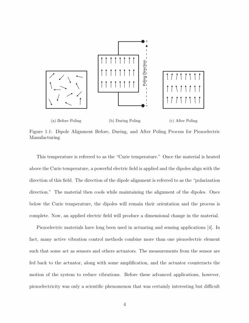
“poling” certain ceramic materials [11]. Before poling, these ceramic materials have dipoles
randomly arranged throughout. To create the piezoelectric effect, these dipoles need to be
aligned with one another. Before poling, an applied electric field would produce no net
extension or contraction in the material because the dipole responses would cancel each
other out. When aligned, the dipole responses would lead to a change in dimensions of the
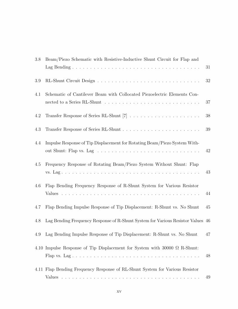
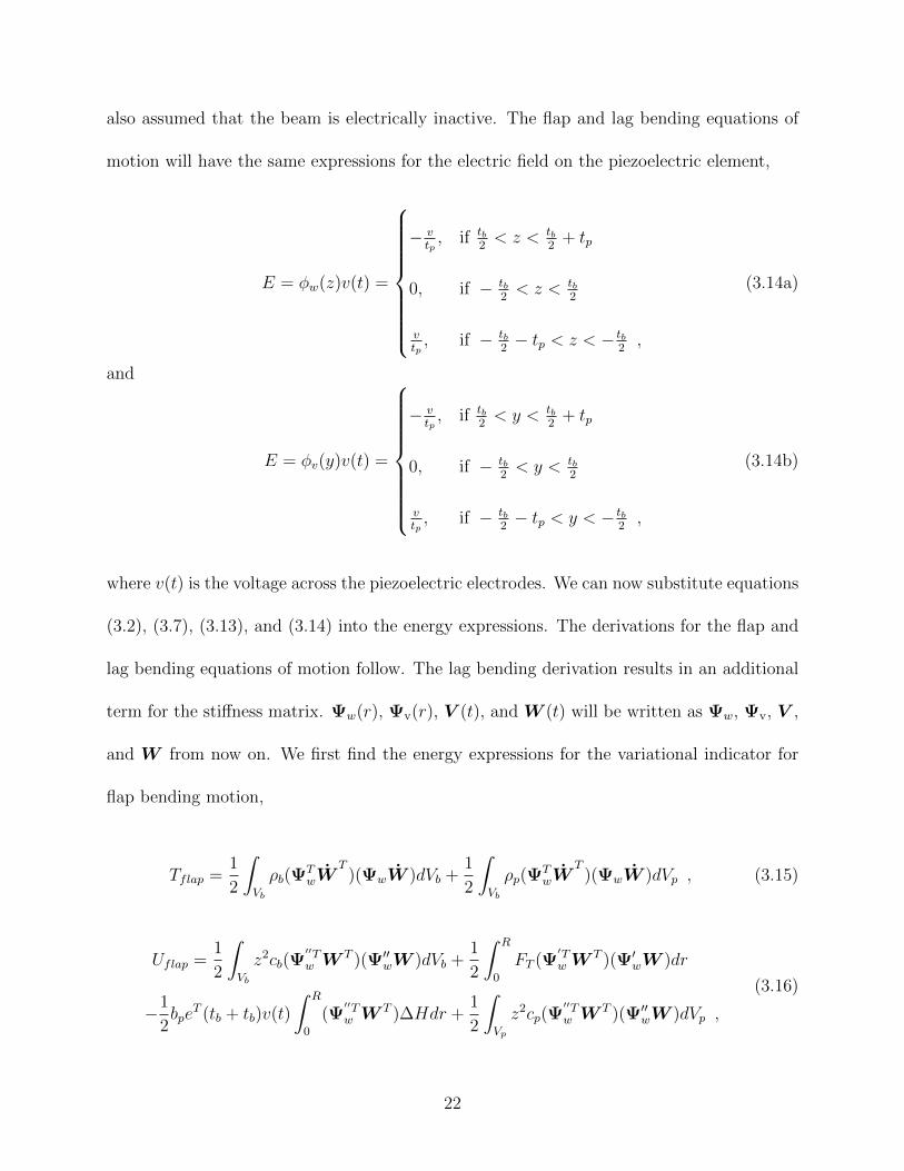
material proportional to the electric field. Figure 1.1 shows the change in dipole alignment
throughout the poling process, which requires the ceramic to be heated above a specific
temperature at which the orientations of the dipoles can be altered.
3
(a) Before Poling
+
-
Polin
g D
irect
ion
(b) During Poling (c) After Poling
Figure 1.1: Dipole Alignment Before, During, and After Poling Process for PiezoelectricManufacturing
This temperature is referred to as the “Curie temperature.” Once the material is heated
above the Curie temperature, a powerful electric field is applied and the dipoles align with the
direction of this field. The direction of the dipole alignment is referred to as the “polarization
direction.” The material then cools while maintaining the alignment of the dipoles. Once
below the Curie temperature, the dipoles will remain their orientation and the process is
complete. Now, an applied electric field will produce a dimensional change in the material.
Piezoelectric materials have long been used in actuating and sensing applications [4]. In
fact, many active vibration control methods combine more than one piezoelectric element
such that some act as sensors and others actuators. The measurements from the sensor are
fed back to the actuator, along with some amplification, and the actuator counteracts the
motion of the system to reduce vibrations. Before these advanced applications, however,
piezoelectricity was only a scientific phenomenon that was certainly interesting but difficult
4
to find applications for. The emergence of World War I fueled the revival of piezoelectric
materials and the hunt for their uses [10]. Paul Langevin suggested that quartz plates could
act as transmitters of high-frequency sound waves underwater. Scientist began using piezo-
electric materials to emit sound waves and record the echo returned by an obstructing object.
This became the basis for sonar. Thankfully, scientists learned not only how to manufacture
these types of materials, but how to achieve piezoelectric parameters over 100 times greater
than those of naturally occurring crystals. This led to the numerous applications found
today for piezoelectric materials.
The significantly larger piezoelectric parameters of human-manufactured piezoelectric
materials are necessary for their use in vibration damping techniques. The exchange of
mechanical and electrical energy between a vibrating structure and a piezoelectric element
is large enough for both active and passive vibration techniques. Therefore, various methods
for vibration damping using piezoelectric materials will now be discussed.
5
CHAPTER 2
LITERATURE REVIEW
2.1 ACTIVE CONSTRAINED LAYER DAMPING
The use of piezoelectric materials as a method for vibration reduction has been a popular
area of research for the past thirty years [1, 2, 12]. One of the early methods of vibration
reduction was through a method called Active Constrained Layer Damping (ACLD). An
ACLD treatment consists of two layers - one active and one passive. The active layer is a
piezoelectric layer and the passive layer is a viscoelastic layer.
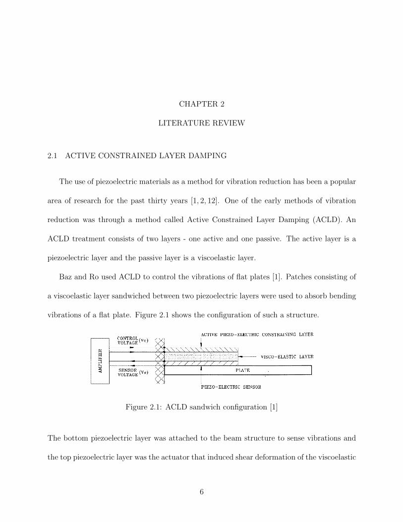
Baz and Ro used ACLD to control the vibrations of flat plates [1]. Patches consisting of
a viscoelastic layer sandwiched between two piezoelectric layers were used to absorb bending
vibrations of a flat plate. Figure 2.1 shows the configuration of such a structure.
Figure 2.1: ACLD sandwich configuration [1]
The bottom piezoelectric layer was attached to the beam structure to sense vibrations and
the top piezoelectric layer was the actuator that induced shear deformation of the viscoelastic
6
layer. The sensor voltage was manipulated and applied as a control voltage to the actuating
piezoelectric element.
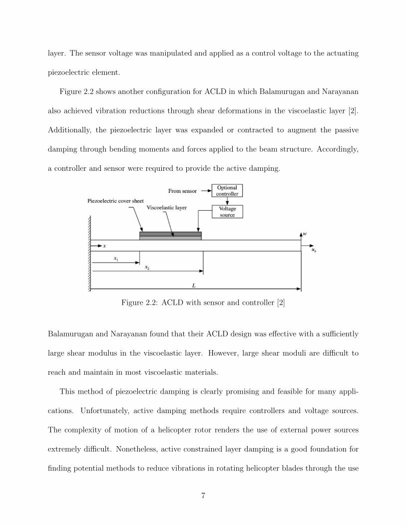
Figure 2.2 shows another configuration for ACLD in which Balamurugan and Narayanan
also achieved vibration reductions through shear deformations in the viscoelastic layer [2].
Additionally, the piezoelectric layer was expanded or contracted to augment the passive
damping through bending moments and forces applied to the beam structure. Accordingly,
a controller and sensor were required to provide the active damping.
Figure 2.2: ACLD with sensor and controller [2]
Balamurugan and Narayanan found that their ACLD design was effective with a sufficiently
large shear modulus in the viscoelastic layer. However, large shear moduli are difficult to
reach and maintain in most viscoelastic materials.
This method of piezoelectric damping is clearly promising and feasible for many appli-
cations. Unfortunately, active damping methods require controllers and voltage sources.
The complexity of motion of a helicopter rotor renders the use of external power sources
extremely difficult. Nonetheless, active constrained layer damping is a good foundation for
finding potential methods to reduce vibrations in rotating helicopter blades through the use
7
of piezoelectric materials.
2.2 ENERGY HARVESTING
A newer application for piezoelectric materials became a popular field of research after
active constrained layer damping had been thoroughly investigated. The frequent use of
batteries to power small wireless electronics can be expensive and inefficient. Batteries must
be replaced when they reach the end of their life. The goal of extracting electrical energy
from a vibrating system to extend a battery’s life or remove the requirement for the battery
altogether became a large area of research in piezoelectric materials [3, 13].
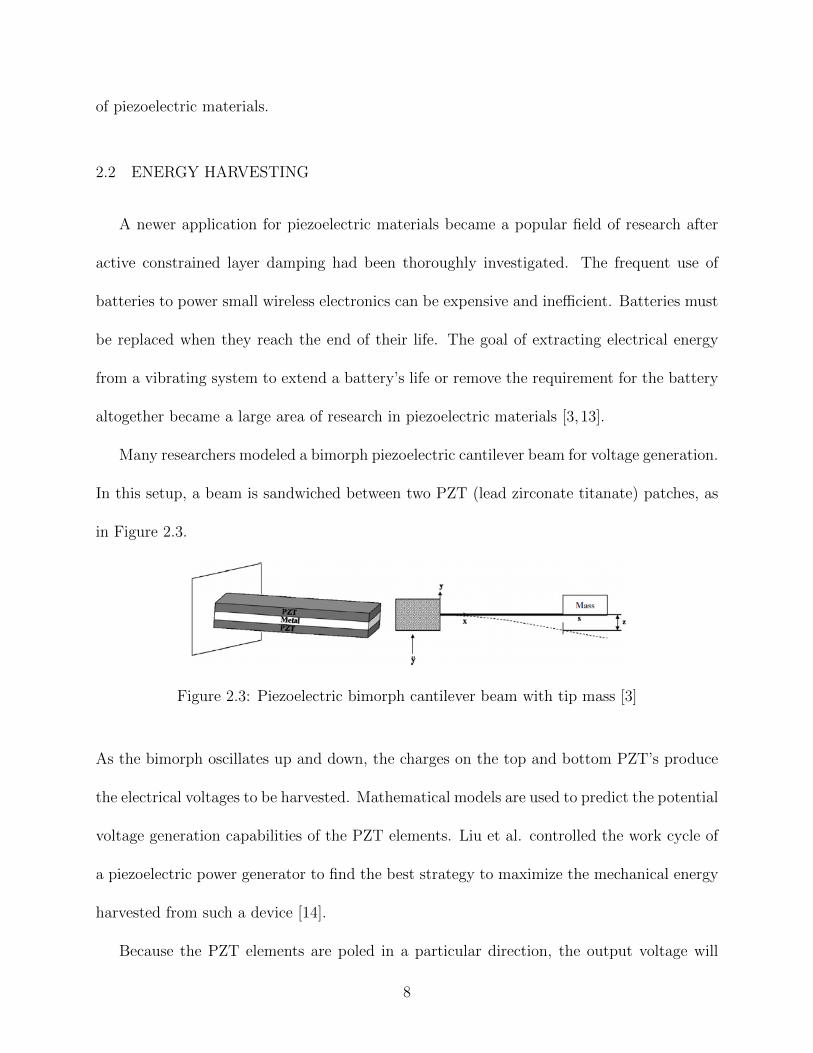
Many researchers modeled a bimorph piezoelectric cantilever beam for voltage generation.
In this setup, a beam is sandwiched between two PZT (lead zirconate titanate) patches, as
in Figure 2.3.
Figure 2.3: Piezoelectric bimorph cantilever beam with tip mass [3]
As the bimorph oscillates up and down, the charges on the top and bottom PZT’s produce
the electrical voltages to be harvested. Mathematical models are used to predict the potential
voltage generation capabilities of the PZT elements. Liu et al. controlled the work cycle of
a piezoelectric power generator to find the best strategy to maximize the mechanical energy
harvested from such a device [14].
Because the PZT elements are poled in a particular direction, the output voltage will
8
be either positive or negative. Lefeuvre et. al. used a “semi-passive” method involving
synchronized switching on voltage sources to artificially increase the voltage delivered by the
piezoelectric elements, thus increasing the amount of energy harvested [15].
These methods are suitable for many vibrating aerospace structures. Vibrations of non-
rotating structures such as wings or fuselages would be appropriate applications for these
types of energy harvesters. Again, however, the rotating aspect of helicopter rotors presents
problems with the practicality of such devices. The concept of removing energy from the
system, however, is key to the proposal of this thesis.
2.3 SHUNT CIRCUITS
A promising method for damping vibrating beams and plates is known as shunt circuit
damping. Many researchers investigated shunt damping techniques that convert mechanical
vibrations into electrical charges to be dissipated through an electrical circuit [4, 5]. The
charge from the piezoelctric element generate a current that is fed through an electrical
circuit, also known as a shunt circuit, with various components. The electric energy can be
released as joule heat as the current flows through a resistive element in the shunt circuit.
This energy dissipation from the system becomes, effectively, a form a structural damping.
As the beam vibrates, more and more energy will be removed until the vibrations have
damped out. This method is ideal for applications that require passive damping methods
with no controllers or voltage sources.
Hagood and von Flotow developed a model for a piezoelectric elements mounted to
a cantilever beam for structural vibration control [4]. In addition addition to a driving
9
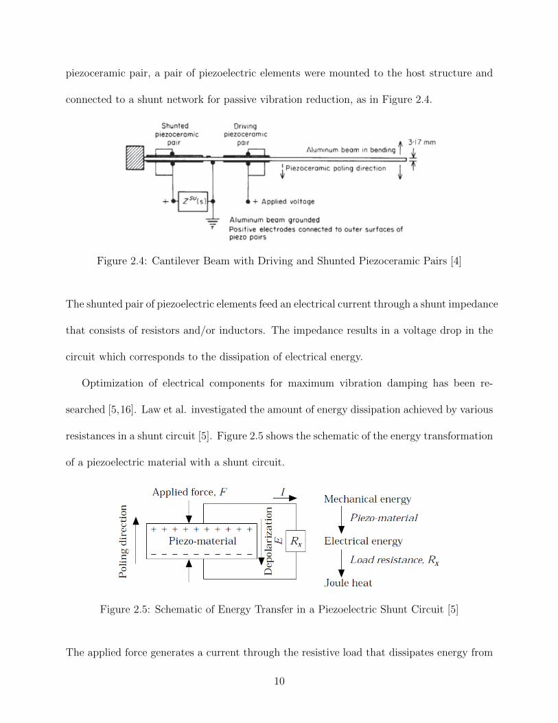
piezoceramic pair, a pair of piezoelectric elements were mounted to the host structure and
connected to a shunt network for passive vibration reduction, as in Figure 2.4.
Figure 2.4: Cantilever Beam with Driving and Shunted Piezoceramic Pairs [4]
The shunted pair of piezoelectric elements feed an electrical current through a shunt impedance
that consists of resistors and/or inductors. The impedance results in a voltage drop in the
circuit which corresponds to the dissipation of electrical energy.
Optimization of electrical components for maximum vibration damping has been re-
searched [5,16]. Law et al. investigated the amount of energy dissipation achieved by various
resistances in a shunt circuit [5]. Figure 2.5 shows the schematic of the energy transformation
of a piezoelectric material with a shunt circuit.
Figure 2.5: Schematic of Energy Transfer in a Piezoelectric Shunt Circuit [5]
The applied force generates a current through the resistive load that dissipates energy from
10
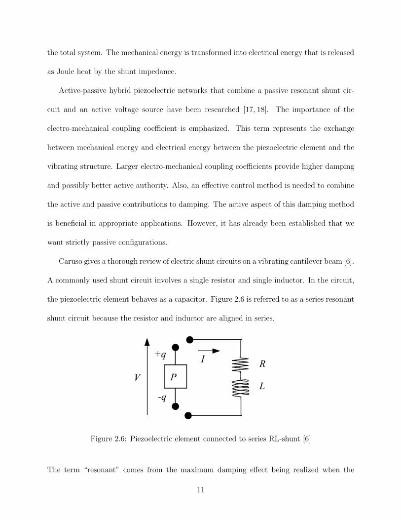
the total system. The mechanical energy is transformed into electrical energy that is released
as Joule heat by the shunt impedance.
Active-passive hybrid piezoelectric networks that combine a passive resonant shunt cir-
cuit and an active voltage source have been researched [17, 18]. The importance of the
electro-mechanical coupling coefficient is emphasized. This term represents the exchange
between mechanical energy and electrical energy between the piezoelectric element and the
vibrating structure. Larger electro-mechanical coupling coefficients provide higher damping
and possibly better active authority. Also, an effective control method is needed to combine
the active and passive contributions to damping. The active aspect of this damping method
is beneficial in appropriate applications. However, it has already been established that we
want strictly passive configurations.
Caruso gives a thorough review of electric shunt circuits on a vibrating cantilever beam [6].
A commonly used shunt circuit involves a single resistor and single inductor. In the circuit,
the piezoelectric element behaves as a capacitor. Figure 2.6 is referred to as a series resonant
shunt circuit because the resistor and inductor are aligned in series.
Figure 2.6: Piezoelectric element connected to series RL-shunt [6]
The term “resonant” comes from the maximum damping effect being realized when the
11
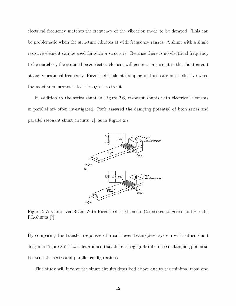
electrical frequency matches the frequency of the vibration mode to be damped. This can
be problematic when the structure vibrates at wide frequency ranges. A shunt with a single
resistive element can be used for such a structure. Because there is no electrical frequency
to be matched, the strained piezoelectric element will generate a current in the shunt circuit
at any vibrational frequency. Piezoelectric shunt damping methods are most effective when
the maximum current is fed through the circuit.
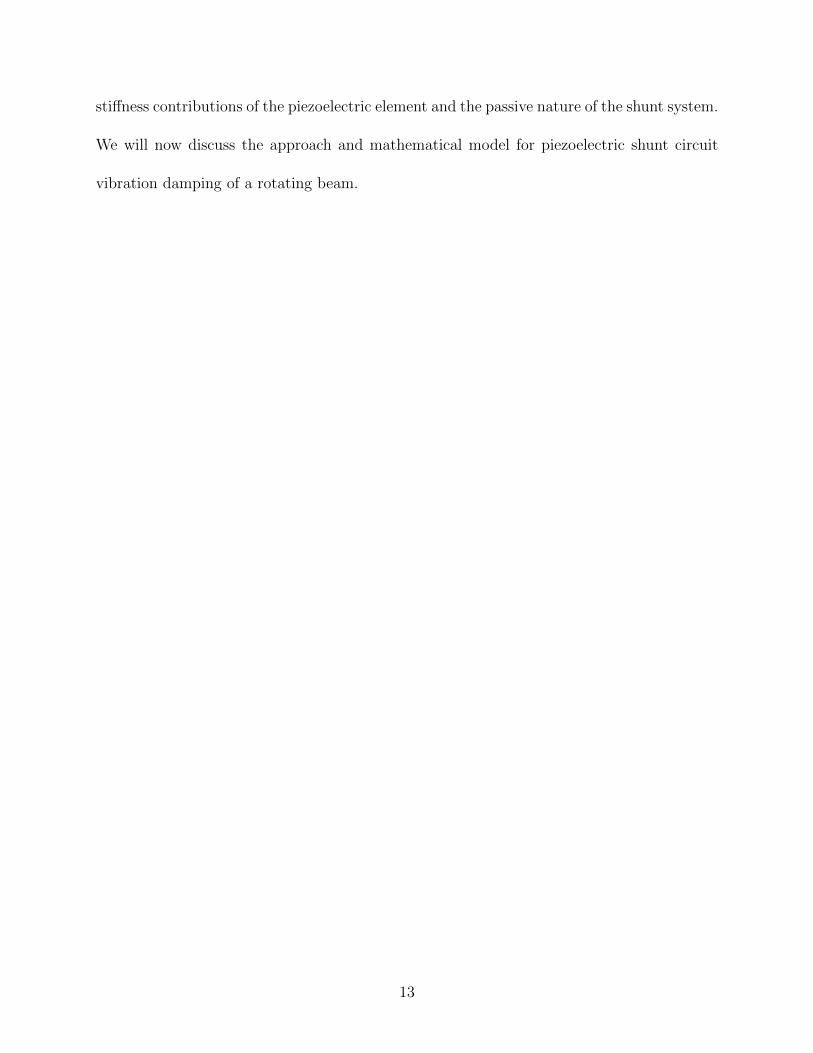
In addition to the series shunt in Figure 2.6, resonant shunts with electrical elements
in parallel are often investigated. Park assessed the damping potential of both series and
parallel resonant shunt circuits [7], as in Figure 2.7.
Figure 2.7: Cantilever Beam With Piezoelectric Elements Connected to Series and ParallelRL-shunts [7]
By comparing the transfer responses of a cantilever beam/piezo system with either shunt
design in Figure 2.7, it was determined that there is negligible difference in damping potential
between the series and parallel configurations.
This study will involve the shunt circuits described above due to the minimal mass and
12
stiffness contributions of the piezoelectric element and the passive nature of the shunt system.
We will now discuss the approach and mathematical model for piezoelectric shunt circuit
vibration damping of a rotating beam.
13
CHAPTER 3
APPROACH
A single degree-of-freedom (DOF) model is developed for a rotating uniform rectangular
cantilever beam with a piezoelectric shunt circuit. Two shunt circuit designs will be con-
sidered for the rotating structure: a simple resistive shunt and a series resistive-inductive
shunt. No inherent structural damping is included in the model. As a result, the damping
seen in the responses will be solely due to the shunt circuit. First, a single mode approx-
imation is employed. The purpose of this is to build a fundamental understanding of the
way the piezoelectric material interacts with a vibrating beam. Next, simulations assuming
multiple modes of vibration are carried out. The damping capabilities of shunting circuits
are assessed for various electrical components and configurations.
Single DOF linear models can be easily represented in state-space form. This simplifies
the simulation process and allows for a preliminary assessment of the shunt damping ca-
pabilities. Two types of bending motion are considered here: flap and lag. Flap bending
(out-of-plane bending) corresponds to displacement in a direction parallel to the axis of ro-
tation. Lag bending (in-plane bending) corresponds to displacement in the plane of rotation.
Due to the presence of rotation, the lag bending equations of motion will have an additional
term in the expression for strain energy. This will be highlighted during the derivation.
The piezoelectric element is assumed to be perfectly bonded to the beam. This implies
that there is no energy loss when mechanical energy is transformed into electrical energy
14
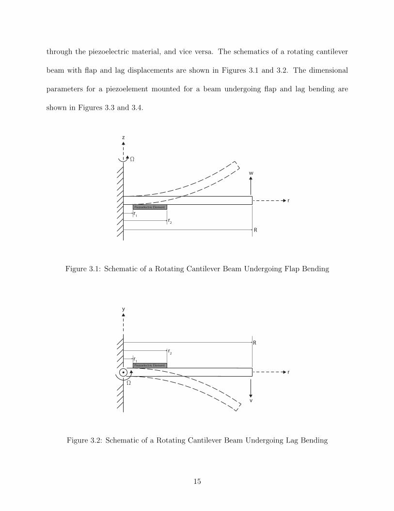
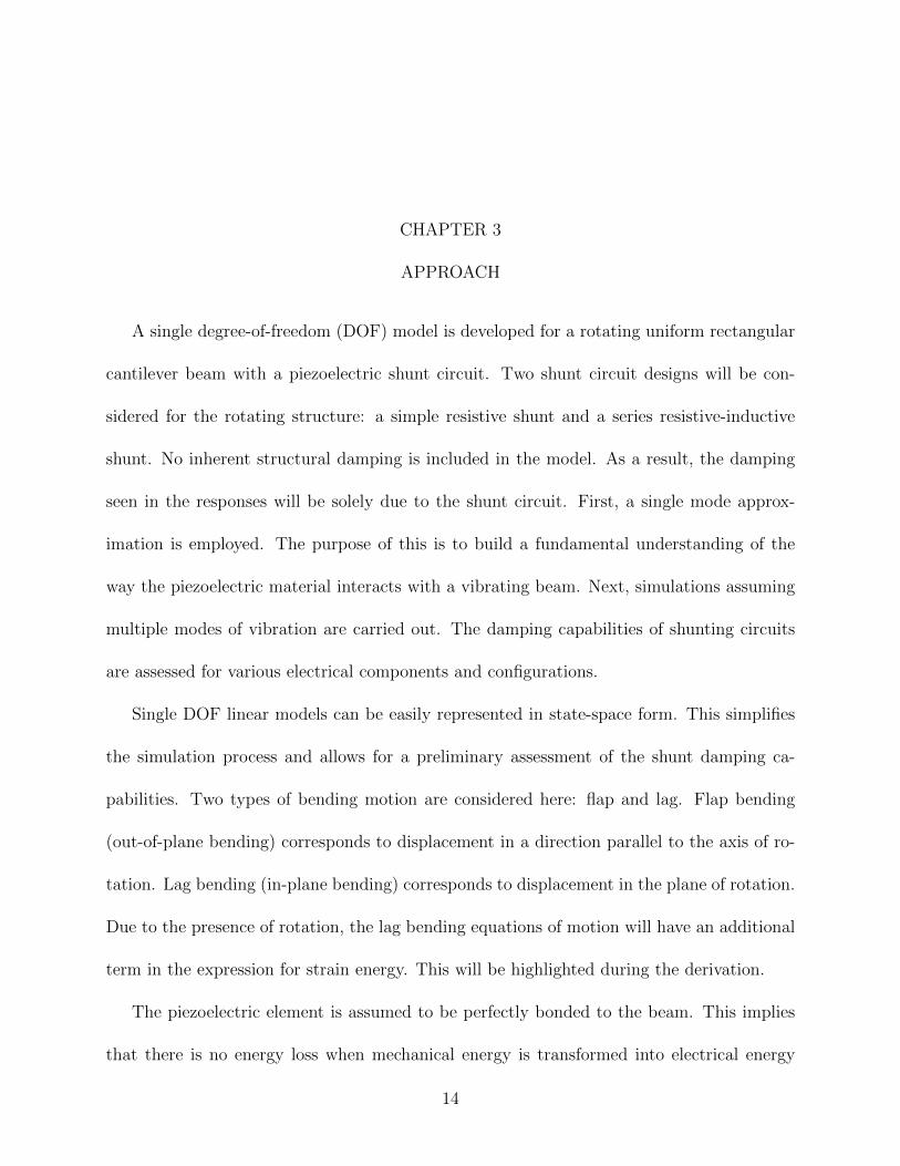
through the piezoelectric material, and vice versa. The schematics of a rotating cantilever
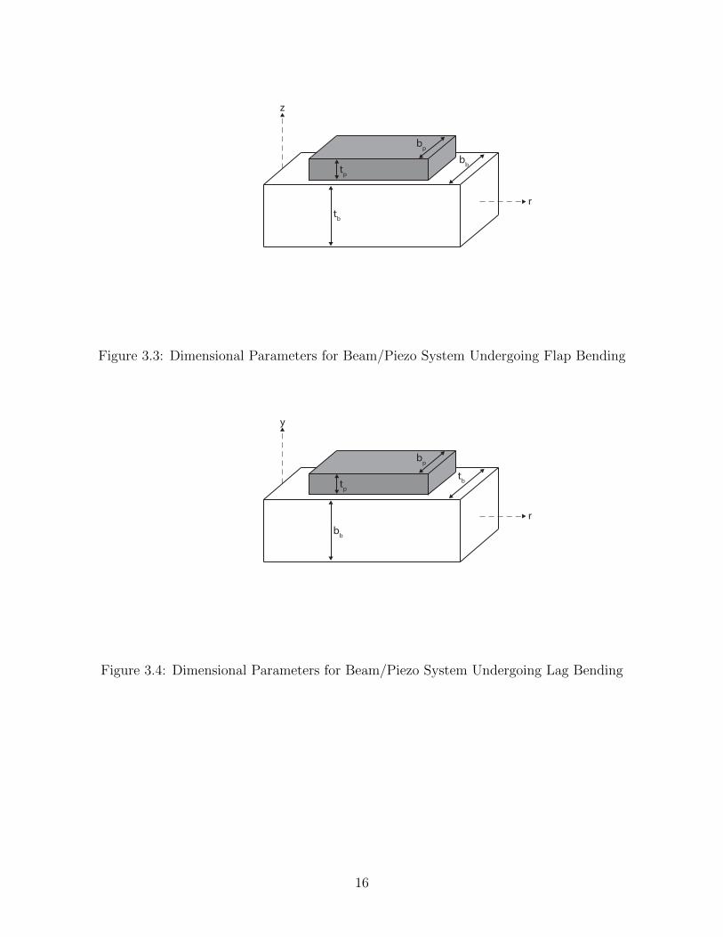
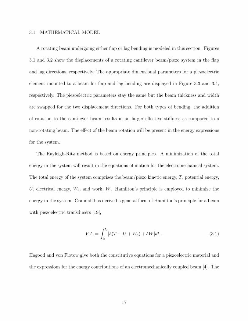
beam with flap and lag displacements are shown in Figures 3.1 and 3.2. The dimensional
parameters for a piezoelement mounted for a beam undergoing flap and lag bending are
shown in Figures 3.3 and 3.4.
w
r
z
Ω
Piezoelectric Element
R
r1r2
Figure 3.1: Schematic of a Rotating Cantilever Beam Undergoing Flap Bending
v
r
y
Ω
Piezoelectric Element
R
r1
r2
Figure 3.2: Schematic of a Rotating Cantilever Beam Undergoing Lag Bending
15
rtb
tp
z
tpbb
bp
Figure 3.3: Dimensional Parameters for Beam/Piezo System Undergoing Flap Bending
r
tbtp
y
tp
bb
bp
Figure 3.4: Dimensional Parameters for Beam/Piezo System Undergoing Lag Bending
16
3.1 MATHEMATICAL MODEL
A rotating beam undergoing either flap or lag bending is modeled in this section. Figures
3.1 and 3.2 show the displacements of a rotating cantilever beam/piezo system in the flap
and lag directions, respectively. The appropriate dimensional parameters for a piezoelectric
element mounted to a beam for flap and lag bending are displayed in Figure 3.3 and 3.4,
respectively. The piezoelectric parameters stay the same but the beam thickness and width
are swapped for the two displacement directions. For both types of bending, the addition
of rotation to the cantilever beam results in an larger effective stiffness as compared to a
non-rotating beam. The effect of the beam rotation will be present in the energy expressions
for the system.
The Rayleigh-Ritz method is based on energy principles. A minimization of the total
energy in the system will result in the equations of motion for the electromechanical system.
The total energy of the system comprises the beam/piezo kinetic energy, T , potential energy,
U , electrical energy, We, and work, W . Hamilton’s principle is employed to minimize the
energy in the system. Crandall has derived a general form of Hamilton’s principle for a beam
with piezoelectric transducers [19],
V.I. =
∫ t2
t1
[δ(T − U +We) + δW ]dt . (3.1)
Hagood and von Flotow give both the constitutive equations for a piezoelectric material and
the expressions for the energy contributions of an electromechanically coupled beam [4]. The
17
constitutive equations are written as
DT
=
εS e
−eT cE
ES
, (3.2)
where D is the vector of electrical displacements, T is the vector of material stresses, εS is
the matrix of dielectric constants, eij are the piezoelectric material constants relating voltage
in the ith direction to stress in the jth direction, cE is the stiffness matrix, E is the vector of
electric fields, and S is the vector of material strains. Bold font represents a quantity that
is an array.
The energy expressions given by Hagood and von Flotow must be augmented. For rotat-
ing beams, additional potential energy terms must be added to account for the strain energy
due to the centrifugal force [20]. The kinetic energy is written as
Tflap =1
2
∫Vb
ρb(∂w
∂t)2dVb +
1
2
∫Vp
ρp(∂w
∂t)2dVp , (3.3a)
and
Tlag =1
2
∫Vb
ρb(∂v
∂t)2dVb +
1
2
∫Vp
ρp(∂v
∂t)2dVp . (3.3b)
The potential energy expressions for flap and lag bending are written below. The potential
energy for lag bending contains one more term than flap bending.
Uflap =1
2
∫Vb
STTdVb +1
2
∫ R
0
FT (∂w
∂r)2dr +
1
2
∫Vp
STTdVp , (3.4a)
18
and
Ulag =1
2
∫Vb
STTdVb +1
2
∫ R
0
FT (∂v
∂r)2dr − 1
2
∫ R
0
mΩ2v2dr +1
2
∫Vp
STTdVp . (3.4b)
Where the centrifugal force is defined as FT =∫VbρbΩ
2rdVb. Equations (3.4a) and (3.4b)
account for the presence of beam rotation. Both flap and lag potential energy expressions
have a term corresponding to the centrifugal force as a result of the rotation. Additionally, lag
bending potential energy has a term representing the in-plane component of the centrifugal
force. The electrical energy expression is the same for both flap and lag bending written as
We =1
2
∫Vp
ETDdVp . (3.5)
Lastly, the virtual work terms are expressed as
δWflap =
nf∑i=1
δw(ri, t)fi(t) +
nq∑j=1
δvqj(t) , (3.6a)
and
δWlag =
nf∑i=1
δv(ri, t)fi(t) +
nq∑j=1
δvqj(t) , (3.6b)
where fi(t) is the external force and qj is the charge on the electrodes of the piezoelectric
patch.
This method assumes that the transverse deflections of a cantilever beam can be ap-
proximated by a series of shape functions that satisfy the geometric boundary conditions of
the problem. The goal is to minimize the error between this approximation and the exact
solution. This is accomplished by applying variational principles.
19
Let us now assume that the transverse deflections, w and v, are defined as
w(r, t) =N∑i=1
Ψw,i(r)Wi(t) =
[Ψw,1(r) Ψw,2(r) . . . Ψw,N(r)
]
W1(t)
W2(t)
...
WN(t)
= Ψw(r)W (t) ,
(3.7a)
and
v(r, t) =N∑i=1
Ψv,i(r)Vi(t) =
[Ψv,1(r) Ψv,2(r) . . . Ψv,N(r)
]
V1(t)
V2(t)
...
VN(t)
= Ψv(r)V (t) ,
(3.7b)
where Ψw,i(r) and Ψv,i(r) are the admissible spatial shape functions and Wi(t) and Vi(t)
are the temporal modal coordinates for flap and lag displacements, respectively. The shape
functions for a cantilever beam are determined by the following boundary conditions [21].
Geometric boundary conditions at the clamped end, r = 0, are
Ψ(0) = 0 anddΨ(0)
dr= 0 . (3.8)
Natural boundary conditions at the free end, r = L, are
d2Ψ(L)
dr2= 0 and
d3Ψ(L)
dr3= 0 . (3.9)
20
The shape functions that satisfy these boundary conditions are written as
Ψi(r) = sin(βir) − sinh(βir) + Ci[cos(βir) − cosh(βir)] , (3.10)
where βi are the roots of the characteristic equation
cos(βiL) cos(βiL) = −1 , (3.11)
and Ci are the mode shape constants determined by
Ci = − sin(βiL) + sinh(βiL)
cos(βiL) + cosh(βiL). (3.12)
There is an infinite set of roots that solve equation (3.10). It is common practice to assume
only the first few modes in vibration approximations. The beam matrices for the single DOF
models will be calculated by the first three modes of vibration.
Some assumptions must be made in addition to equation (3.7). We will assume Euler-
Bernoulli beam theory, that is, the strain at the surface of the beam can be written as a
function of the second derivative of displacement and distance from the neutral axis,
Sflap = −z∂2w(r, t)
∂r2= −zΨ′′w,i(r)Wi(t) , (3.13a)
and
Slag = −y∂2v(r, t)
∂r2= −yΨ′′v,i(r)Vi(t) . (3.13b)
We will assume that the electric potential across the piezoelectric element is constant. It is
21
also assumed that the beam is electrically inactive. The flap and lag bending equations of
motion will have the same expressions for the electric field on the piezoelectric element,
E = φw(z)v(t) =
− vtp, if tb
2< z < tb
2+ tp
0, if − tb2< z < tb
2
vtp, if − tb
2− tp < z < − tb
2,
(3.14a)
and
E = φv(y)v(t) =
− vtp, if tb
2< y < tb
2+ tp
0, if − tb2< y < tb
2
vtp, if − tb
2− tp < y < − tb
2,
(3.14b)
where v(t) is the voltage across the piezoelectric electrodes. We can now substitute equations
(3.2), (3.7), (3.13), and (3.14) into the energy expressions. The derivations for the flap and
lag bending equations of motion follow. The lag bending derivation results in an additional
term for the stiffness matrix. Ψw(r), Ψv(r), V (t), and W (t) will be written as Ψw, Ψv, V ,
and W from now on. We first find the energy expressions for the variational indicator for
flap bending motion,
Tflap =1
2
∫Vb
ρb(ΨTwW
T)(ΨwW )dVb +
1
2
∫Vb
ρp(ΨTwW
T)(ΨwW )dVp , (3.15)
Uflap =1
2
∫Vb
z2cb(Ψ′′Tw W T )(Ψ′′wW )dVb +
1
2
∫ R
0
FT (Ψ′Tw W T )(Ψ′wW )dr
−1
2bpe
T (tb + tb)v(t)
∫ R
0
(Ψ′′Tw W T )∆Hdr +
1
2
∫Vp
z2cp(Ψ′′Tw W T )(Ψ′′wW )dVp ,
(3.16)
22
We =1
2bpe(tb + tb)v(t)
∫ R
0
(Ψ′′wW )∆Hdr +2εbptp
v(t)v(t)
∫ R
0
∆Hdr , (3.17)
and
δWflap =
nf∑i=1
δ(Ψw(ri)W (t))fi(ri) +
nq∑j=1
δvqj(t) , (3.18)
where ∆H = [H(r − r1) −H(r − r2)], and H is the Heaviside function. This ensures that
the radial integral only accounts for the piezoelectric element along the length that it is
attached. e can be written as e = dijcp. Now we can take the variations of the equations
above, substitute into the variational indicator, equation (3.1), and introduce terms that will
simplify the variational indicator to provide some physical insight to the equations above
V Iflap =
∫ t2
t1
[δWTMb,flapW + δW
TMp,flapW + δW TKb,flapW + δW TKp,flapW
−δW TΘflapv(t) + δv(t)ΘTflapW + δv(t)Cpv(t)
+
nf∑i=1
δW (t)(ΨTw(ri)fi(t)) +
nq∑j=1
δvqj(t) .
(3.19)
In equation (3.19), Mb and Mp are the beam and piezoelectric mass matrices defined by
Mb,flap =
∫Vb
ρbΨTwΨwdVb ,
Mp,flap =
∫Vp
ρpΨTwΨwdVp .
(3.20)
Kb and Kp are the beam and piezoelectric stiffness matrices, respectively, defined by
Kb,flap =
∫Vb
z2cbΨ′′Tw Ψ′′wdVb +
∫Vb
FTΨ′Tw Ψ′wdVb ,
Kp,flap =
∫Vp
z2cpΨ′′Tw Ψ′′wdVp .
(3.21)
23
Θ is the electromechanical coupling matrix determined by
Θflap = bpd31cp(tb + tp)
∫ R
0
Ψ′′Tw ∆Hdr . (3.22)
Cp is the matrix representing the inherent capacitance of the piezoelectric material
Cp =2εbptp
∫ R
0
∆Hdr . (3.23)
We define the modal forcing vector as
F z =
nf∑i=1
ΨTw(floc,i)fi(t) . (3.24)
The two following equations of motion are derived by integrating the variational indicator
by parts and collecting the coefficients of the variations δW and δv(t). In this case, we only
have one shunt circuit connected to the piezoelectric element. Therefore,∑nq
j=1 δvqj(t) =
δvq(t). The first equation represents the mechanical behavior of the system while the second
shows the electrical behavior of the system:
(Mb,flap +Mp,flap)W + (Kb,flap +Kp,flap)W − Θflapv(t) = F z , (3.25)
ΘTflapW + Cpv(t) = q(t) . (3.26)
The above derivation will be repeated for lag bending motion. The same steps will be
24
taken to arrive at the electromechanical equations of motion. The energy expressions are
Tlag =1
2
∫Vb
ρb(ΨTv V
T)(ΨvV )dVb +
1
2
∫Vb
ρp(ΨTv V
T)(ΨvV )dVp , (3.27)
Ulag =1
2
∫Vb
z2cb(Ψ′′Tv V T )(Ψ′′vV )dVb +
1
2
∫ R
0
FT (Ψ′Tv V T )(Ψ′vV )dr
−1
2
∫Vb
ρbΩ2(ΨvV )(ΨvV )dVb −
1
2bpe
T (tb + tb)v(t)
∫ R
0
(Ψ′′Tv V T )∆Hdr
+1
2
∫Vp
z2cp(Ψ′′Tv V T )(Ψ′′vV )dVp ,
(3.28)
We =1
2bpe(tb + tb)v(t)
∫ R
0
(Ψ′′vV )∆Hdr +2εbptp
v(t)v(t)
∫ R
0
∆Hdr , (3.29)
and
δWlag =
nf∑i=1
δ(Ψv(ri)V (t))fi(ri) +
nq∑j=1
δvqj(t) . (3.30)
Taking the variations of the energy expressions and substituting into (3.1), we will arrive at
an expression for the variational indicator similar to that for flap bending,
V Ilag =
∫ t2
t1
[δVTMb,lagV + δV
TMp,lagV + δV TKb,lagV + δV TKp,lagV
−δV TΘlagv(t) + δv(t)ΘTlagV + δv(t)Cpv(t)
+
nf∑i=1
δV (t)(ΨTv (ri)fi(t)) +
nq∑j=1
δvqj(t) .
(3.31)
As in (3.19), Mb and Mp in (3.31) are mass matrices defined by
Mb,lag =
∫Vb
ρbΨTv ΨvdVb ,
Mp,lag =
∫Vb
ρbΨTv ΨvdVb .
(3.32)
25
Kb and Kp are stiffness matrices and are written as
Kb,lag =
∫Vb
z2cbΨ′′Tv Ψ′′vdVb +
∫Vb
FTΨ′Tv Ψ′vdVb −
∫Vb
ρbΩ2ΨT
v ΨvdVb ,
Kp,lag =
∫Vp
z2cpΨ′′Tv Ψ′′vdVp .
(3.33)
Θ is the electromechanical coupling matrix determined by
Θlag = bpd31cp(tb + tp)
∫ R
0
Ψ′′Tv ∆Hdr . (3.34)
Cp is the matrix representing the inherent capacitance of the piezoelectric material
Cp =2εbptp
∫ R
0
∆Hdr . (3.35)
We define the modal forcing vector as
F x =
nf∑i=1
ΨTv (floc,i)fi(t) . (3.36)
As in the derivation for flap bending, the variational indicator is integrated by parts and
the coefficients of δV and δv(t) are collected. Again, because we only have one shunt
circuit connected to the piezoelectric element, we can write∑nq
j=1 δvqj(t) = δvq(t). The
first equation represents the mechanical behavior of the lag bending motion and the second
equation shows the electrical behavior:
(Mb,lag +Mp,lag)V + (Kb,lag +Kp,lag)V − Θlagv(t) = F x , (3.37)
26
ΘTlagV + Cpv(t) = q(t) . (3.38)
The electromechanical models we have derived account for the mechanical vibrations of
the beam and the charges generated by the piezoelectric elements due to the displacement
of the beam. However, there is no present form of energy dissipation. Simulating equations
(3.25) and (3.26) for flap bending or (3.37) and (3.38) for lag bending would only show the
exchange between mechanical and electrical energy. Accordingly, we need to introduce an
expression involving the electrical components of the shunt circuit.
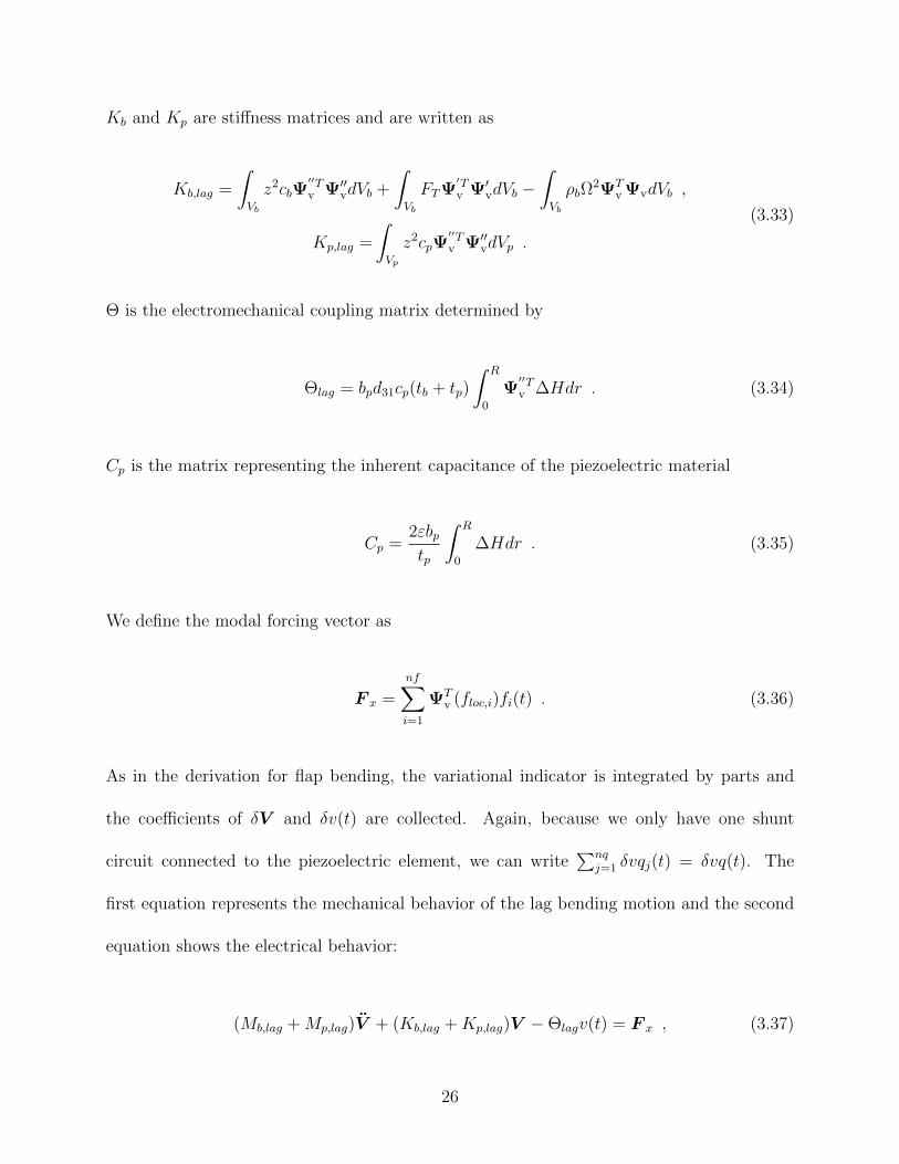
3.2 RESISTIVE SHUNT CIRCUIT
The derivations for the following shunt circuit systems will be shown for flap bending
only. The equations for flap and lag bending motion are identical after the appropriate
stiffness matrices have been incorporated. Accordingly, it would be repetitive to include
the derivations for both types of motion. When we arrive at the final equations for the
system, the flap and lag mass, stiffness, and electromechanical coupling matrices will be
interchangeable. Two shunt circuit designs will be examined. First, a circuit involving a
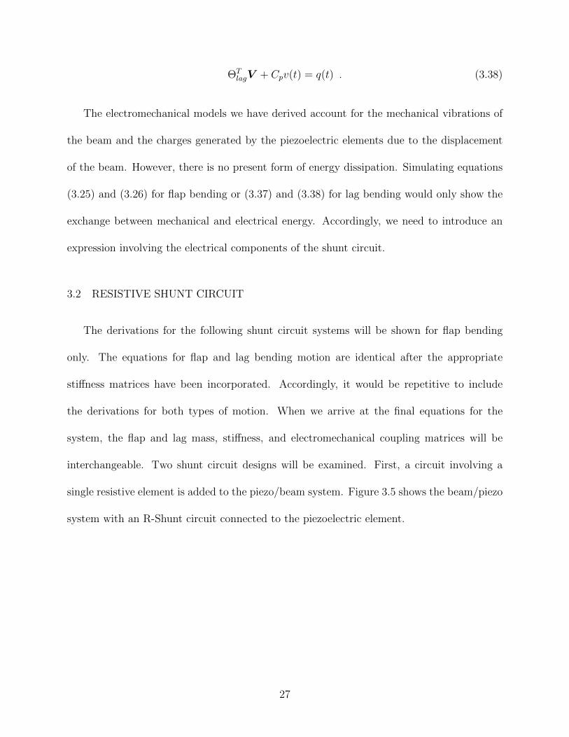
single resistive element is added to the piezo/beam system. Figure 3.5 shows the beam/piezo
system with an R-Shunt circuit connected to the piezoelectric element.
27
w
r
z
Ω
Piezoelectric Element
R
(a) Flap Bending
v
r
y
Ω
Piezoelectric Element
R
(b) Lag Bending
Figure 3.5: Beam/Piezo Schematic with Resistive Shunt Circuit for Flap and Lag Bending
Because we are considering a uniform cantilever beam and have made the assumptions
in (3.13), it does not matter which side we attach the piezoelectric element and shunt. This
simple resistive circuit will dissipate energy at all frequencies. It is advantageous to use a
circuit like this when there is not a dominant vibrational frequency or mode. Figure 3.6
shows the equivalent circuit design of the shunt attached to a piezoelectric element.
v R
−
+
vsh
q +
q −
(a) Voltage Source Representation
I = q R
Ish
Cp
(b) Current Source Representation
Figure 3.6: R-Shunt Circuit Design
The piezoelectric element can be represented as either a voltage or current source. The
impedance of the shunt electrical elements results in a drop in voltage according to Ohm’s law.
28
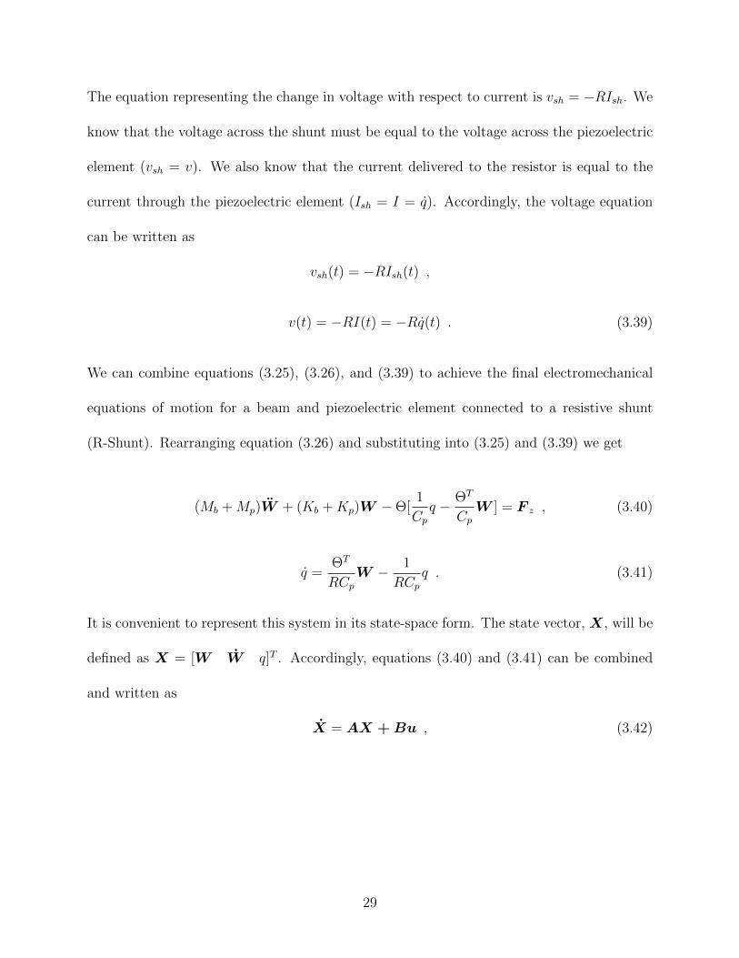
The equation representing the change in voltage with respect to current is vsh = −RIsh. We
know that the voltage across the shunt must be equal to the voltage across the piezoelectric
element (vsh = v). We also know that the current delivered to the resistor is equal to the
current through the piezoelectric element (Ish = I = q). Accordingly, the voltage equation
can be written as
vsh(t) = −RIsh(t) ,
v(t) = −RI(t) = −Rq(t) . (3.39)
We can combine equations (3.25), (3.26), and (3.39) to achieve the final electromechanical
equations of motion for a beam and piezoelectric element connected to a resistive shunt
(R-Shunt). Rearranging equation (3.26) and substituting into (3.25) and (3.39) we get
(Mb +Mp)W + (Kb +Kp)W − Θ[1
Cp
q − ΘT
Cp
W ] = F z , (3.40)
q =ΘT
RCp
W − 1
RCp
q . (3.41)
It is convenient to represent this system in its state-space form. The state vector, X, will be
defined as X = [W W q]T . Accordingly, equations (3.40) and (3.41) can be combined
and written as
X = AX + Bu , (3.42)
29
where u is the input and the matrices A and B are written as
A =
[0]N×N [I]N×N [0]N×1
−(Mb +Mp)−1[Kb +Kp + ΘΘT
Cp] −(Mb +Mp)
−1CbΘCp
ΘT
RCp[0]1×N
−1RCp
, (3.43)
and
B =
[0]N×1
(Mb +Mp)−1F z
0
. (3.44)
The output can be defined by
Y = CX . (3.45)
In the case of this thesis, the output of interest is usually tip displacement. The matrix, C,
corresponding to that output is written as
C =
[Ψ(R) [0]1×N 0
]. (3.46)
3.3 RESISTIVE-INDUCTIVE SHUNT CIRCUIT
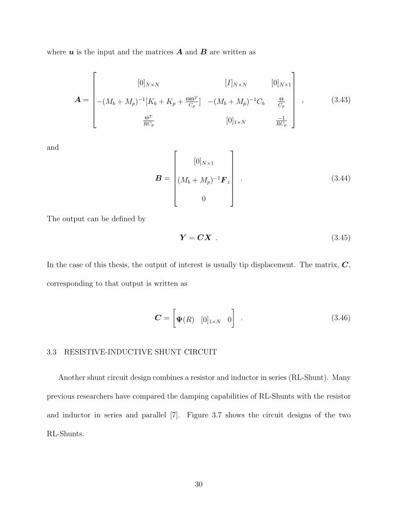
Another shunt circuit design combines a resistor and inductor in series (RL-Shunt). Many
previous researchers have compared the damping capabilities of RL-Shunts with the resistor
and inductor in series and parallel [7]. Figure 3.7 shows the circuit designs of the two
RL-Shunts.
30
L
RPie
zoE
lem
ent
(a) Elements in Series
LR
Pie
zoe
Ele
men
t
(b) Elements in Parallel
Figure 3.7: RL-Shunt Circuit Designs: Series vs. Parallel
It was found that there is little difference between the two types of RL-Shunt designs. Accord-
ingly, only a series RL-Shunt will be examined due to its comparatively simpler integration
into the electromechanical model.
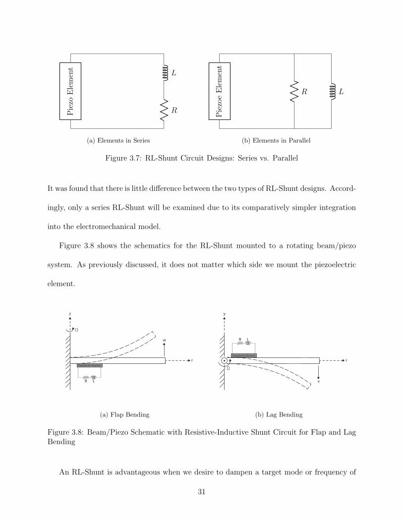
Figure 3.8 shows the schematics for the RL-Shunt mounted to a rotating beam/piezo
system. As previously discussed, it does not matter which side we mount the piezoelectric
element.
w
r
z
Ω
Piezoelectric Element
R L
(a) Flap Bending
v
r
y
Ω
Piezoelectric Element
R L
(b) Lag Bending
Figure 3.8: Beam/Piezo Schematic with Resistive-Inductive Shunt Circuit for Flap and LagBending
An RL-Shunt is advantageous when we desire to dampen a target mode or frequency of
31
vibration. The electrical frequency can be adjusted by altering the inductance. When the
electrical frequency matches the vibration frequency of the structure, the maximum amount
of energy will be dissipated. The downside to this method is the loss of damping potential
when the structure vibrates at a wide range of frequencies. Figure 3.9 shows the equivalent
circuit designs of an RL-Shunt connected to a piezoelectric element.
v
L
R
−
+
vsh
q +
q −
(a) Voltage Source Representation
I = q
L
R
Cp
Ish
(b) Current Source Representation
Figure 3.9: RL-Shunt Circuit Design
As the case was for the R-Shunt circuit, the piezoelectric element in an RL-Shunt circuit can
be represented as either a voltage or current source. The equation for the voltage drop as a
result of the impedance of the shunt circuit elements is vsh = −LIsh − RIsh. We know that
the piezoelectric voltage and shunt voltages must be equal (vsh = v) and that the current
from the piezoelectric element matches the current delivered to the resistor and inductor
(Ish = I = q). As in equation (3.39), Ohm’s law is used to find the change in voltage across
the electrical elements in the R-Shunt circuit:
vsh = −LIsh −RIsh ,
v = −LI −RI ,
32
v = −Lq −Rq . (3.47)
We must also be able to calculate the electrical frequency of an RL-Shunt circuit so that we
can tune it to the target mode frequency. The mechanical-electrical equivalent components
are shown in Table 3.1.
MECHANICAL COMPONENT ELECTRICAL COMPONENT
Mass, M Inductance, L
Damping, C Resistance, R
Compliance, K−1 Capacitance, Cp
Table 3.1: Equivalent Mechanical and Electrical Components in Equations of Motion
Therefore, the expression for electrical frequency is found to be
ωe =
√1
LCp
. (3.48)
Following the same method we used to derive the state-space representation for the R-
Shunt, we substitute equation (3.26) into equations (3.25) and (3.39) to get the equations of
motion:
(Mb +Mp)W + (Kb +Kp)W − Θ[1
Cp
q − ΘT
Cp
W ] = F z , (3.49)
q =ΘT
LCp
W − 1
LCp
q − R
Lq . (3.50)
The state vector, X, for this system will now contain the time derivative of both displacement
and electric charge: X = [W W q q]T . In state-space form, equations (3.49) and (3.50)
33
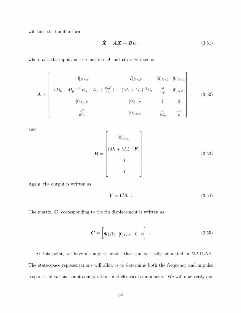
will take the familiar form
X = AX + Bu , (3.51)
where u is the input and the matrices A and B are written as
A =
[0]N×N [I]N×N [0]N×1 [0]N×1
−(Mb +Mp)−1[Kb +Kp + ΘΘT
Cp] −(Mb +Mp)
−1CbΘCp
[0]N×1
[0]1×N [0]1×N 1 0
ΘT
RCp[0]1×N
−1LCp
−RL
, (3.52)
and
B =
[0]N×1
(Mb +Mp)−1F z
0
0
. (3.53)
Again, the output is written as
Y = CX . (3.54)
The matrix, C, corresponding to the tip displacement is written as
C =
[Ψ(R) [0]1×N 0 0
]. (3.55)
At this point, we have a complete model that can be easily simulated in MATLAB.
The state-space representations will allow is to determine both the frequency and impulse
responses of various shunt configurations and electrical components. We will now verify our
34
model and then assess the damping capabilities of a piezoelectric shunt circuit on a rotating
beam.
35
CHAPTER 4
VERIFICATION AND RESULTS
This chapter will show the verification and results of the model derived in Chapter 3.
The damping capabilities of the model for a non-rotating beam with an RL-Shunt will be
verified for a number of resistors. The frequencies of the model for a rotating beam will also
be verified by comparing to simulation data from the HART-II Blade data [22]. This will
give us confidence that our electromechanical model is correct.
The results for a rotating vibrating beam with a piezoelectric shunt circuit will be pre-
sented for various electrical components. The damping capabilities of various circuits and
components will be assessed through the frequency and impulse responses of each system.
4.1 NON-ROTATING BEAM VERIFICATION
It is important to verify that the electromechanical model derived in the previous chapter
is correct. Park developed an electromechanical model for RL-Shunts on non-rotating beams
and showed the damping capabilities of the system for various resistor values [7]. A pair of
piezoelectric elements were mounted on top and bottom of the cantilever beam. The two
piezoelements were connected in series to a single shunt, as shown in Figure 4.1.
36
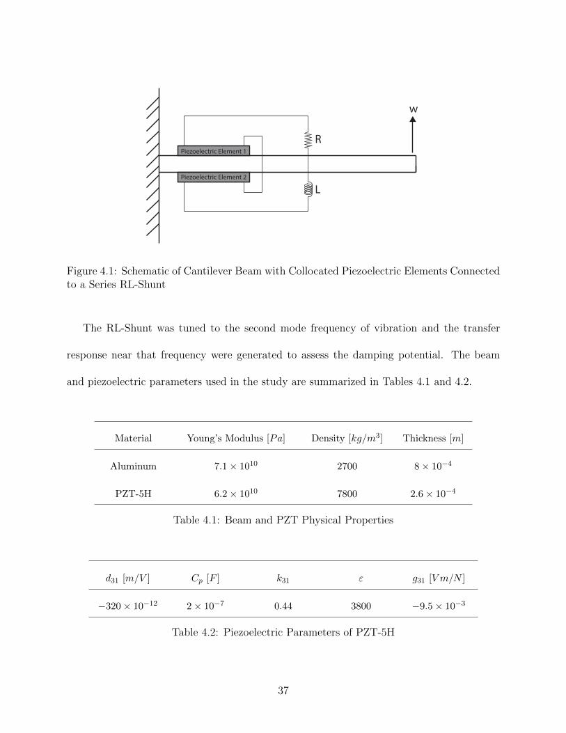
w
Piezoelectric Element 2
Piezoelectric Element 1
R
L
Figure 4.1: Schematic of Cantilever Beam with Collocated Piezoelectric Elements Connectedto a Series RL-Shunt
The RL-Shunt was tuned to the second mode frequency of vibration and the transfer
response near that frequency were generated to assess the damping potential. The beam
and piezoelectric parameters used in the study are summarized in Tables 4.1 and 4.2.
Material Young’s Modulus [Pa] Density [kg/m3] Thickness [m]
Aluminum 7.1 × 10¹⁰ 2700 8 × 10⁻⁴
PZT-5H 6.2 × 10¹⁰ 7800 2.6 × 10⁻⁴
Table 4.1: Beam and PZT Physical Properties
d31 [m/V ] Cp [F ] k31 ε g31 [V m/N ]
−320 × 10−12 2 × 10⁻⁷ 0.44 3800 −9.5 × 10⁻³
Table 4.2: Piezoelectric Parameters of PZT-5H
37
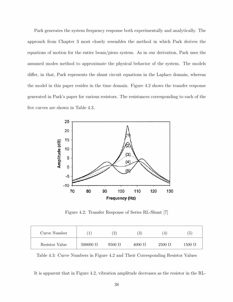
Park generates the system frequency response both experimentally and analytically. The
approach from Chapter 3 most closely resembles the method in which Park derives the
equations of motion for the entire beam/piezo system. As in our derivation, Park uses the
assumed modes method to approximate the physical behavior of the system. The models
differ, in that, Park represents the shunt circuit equations in the Laplace domain, whereas
the model in this paper resides in the time domain. Figure 4.2 shows the transfer response
generated in Park’s paper for various resistors. The resistances corresponding to each of the
five curves are shown in Table 4.3.
Figure 4.2: Transfer Response of Series RL-Shunt [7]
Curve Number (1) (2) (3) (4) (5)
Resistor Value 500000 Ω 9500 Ω 4000 Ω 2500 Ω 1500 Ω
Table 4.3: Curve Numbers in Figure 4.2 and Their Corresponding Resistor Values
It is apparent that in Figure 4.2, vibration amplitude decreases as the resistor in the RL-
38
Shunt decreases. After a certain value, the two peaks on either side of the target frequency
appear. This is analagous to the behavior of a mechanical absorber. The transfer response for
the same beam/piezo parameters is now found using the electromechanical model developed
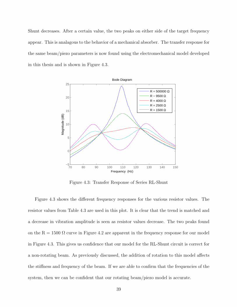
in this thesis and is shown in Figure 4.3.
70 80 90 100 110 120 130 140 150−5
0
5
10
15
20
25
Mag
nitu
de (
dB)
Bode Diagram
Frequency (Hz)
R = 500000 Ω
R − 9500 ΩR = 4000 ΩR = 2500 ΩR = 1500 Ω
Figure 4.3: Transfer Response of Series RL-Shunt
Figure 4.3 shows the different frequency responses for the various resistor values. The
resistor values from Table 4.3 are used in this plot. It is clear that the trend is matched and
a decrease in vibration amplitude is seen as resistor values decrease. The two peaks found
on the R = 1500 Ω curve in Figure 4.2 are apparent in the frequency response for our model
in Figure 4.3. This gives us confidence that our model for the RL-Shunt circuit is correct for
a non-rotating beam. As previously discussed, the addition of rotation to this model affects
the stiffness and frequency of the beam. If we are able to confirm that the frequencies of the
system, then we can be confident that our rotating beam/piezo model is accurate.
39
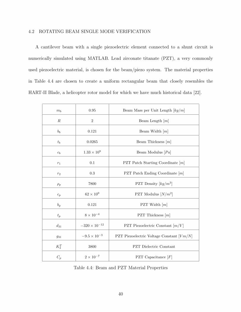
4.2 ROTATING BEAM SINGLE MODE VERIFICATION
A cantilever beam with a single piezoelectric element connected to a shunt circuit is
numerically simulated using MATLAB. Lead zirconate titanate (PZT), a very commonly
used piezoelectric material, is chosen for the beam/piezo system. The material properties
in Table 4.4 are chosen to create a uniform rectangular beam that closely resembles the
HART-II Blade, a helicopter rotor model for which we have much historical data [22].
mb 0.95 Beam Mass per Unit Length [kg/m]
R 2 Beam Length [m]
bb 0.121 Beam Width [m]
tb 0.0265 Beam Thickness [m]
cb 1.33 × 10⁹ Beam Modulus [Pa]
r1 0.1 PZT Patch Starting Coordinate [m]
r2 0.3 PZT Patch Ending Coordinate [m]
ρp 7800 PZT Density [kg/m3]
cp 62 × 109 PZT Modulus [N/m2]
bp 0.121 PZT Width [m]
tp 8 × 10⁻⁴ PZT Thickness [m]
d31 −320 × 10−12 PZT Piezoelectric Constant [m/V ]
g31 −9.5 × 10⁻³ PZT Piezoelectric Voltage Constant [V m/N ]
KT3 3800 PZT Dielectric Constant
Cp 2 × 10⁻⁷ PZT Capacitance [F ]
Table 4.4: Beam and PZT Material Properties
40
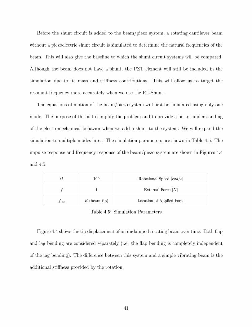
Before the shunt circuit is added to the beam/piezo system, a rotating cantilever beam
without a piezoelectric shunt circuit is simulated to determine the natural frequencies of the
beam. This will also give the baseline to which the shunt circuit systems will be compared.
Although the beam does not have a shunt, the PZT element will still be included in the
simulation due to its mass and stiffness contributions. This will allow us to target the
resonant frequency more accurately when we use the RL-Shunt.
The equations of motion of the beam/piezo system will first be simulated using only one
mode. The purpose of this is to simplify the problem and to provide a better understanding
of the electromechanical behavior when we add a shunt to the system. We will expand the
simulation to multiple modes later. The simulation parameters are shown in Table 4.5. The
impulse response and frequency response of the beam/piezo system are shown in Figures 4.4
and 4.5.
Ω 109 Rotational Speed [rad/s]
f 1 External Force [N ]
floc R (beam tip) Location of Applied Force
Table 4.5: Simulation Parameters
Figure 4.4 shows the tip displacement of an undamped rotating beam over time. Both flap
and lag bending are considered separately (i.e. the flap bending is completely independent
of the lag bending). The difference between this system and a simple vibrating beam is the
additional stiffness provided by the rotation.
41
0 0.2 0.4 0.6 0.8 1 1.2 1.4 1.6 1.8 2−0.025
−0.02
−0.015
−0.01
−0.005
0
0.005
0.01
0.015
0.02
0.025Tip Displacement for Impulse Load
Time [s]
Dis
plac
emen
t [m
]
Flap Bending
Lag Bending
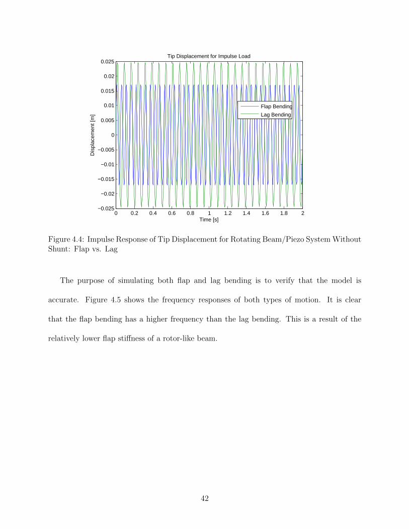
Figure 4.4: Impulse Response of Tip Displacement for Rotating Beam/Piezo System WithoutShunt: Flap vs. Lag
The purpose of simulating both flap and lag bending is to verify that the model is
accurate. Figure 4.5 shows the frequency responses of both types of motion. It is clear
that the flap bending has a higher frequency than the lag bending. This is a result of the
relatively lower flap stiffness of a rotor-like beam.
42
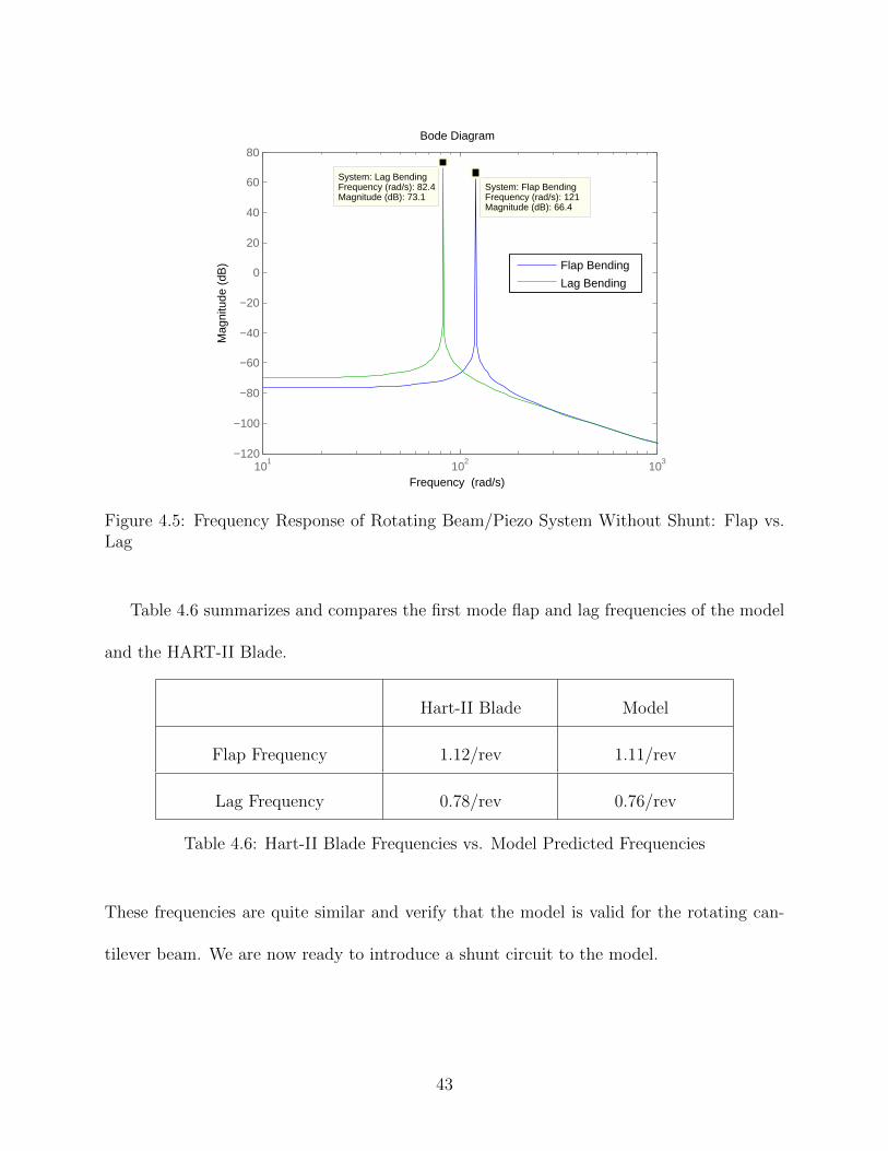
Bode Diagram
Frequency (rad/s)101 102 103
−120
−100
−80
−60
−40
−20
0
20
40
60
80
System: Flap Bending Frequency (rad/s): 121Magnitude (dB): 66.4
Mag
nitu
de (
dB)
System: Lag BendingFrequency (rad/s): 82.4Magnitude (dB): 73.1
Flap Bending
Lag Bending
Figure 4.5: Frequency Response of Rotating Beam/Piezo System Without Shunt: Flap vs.Lag
Table 4.6 summarizes and compares the first mode flap and lag frequencies of the model
and the HART-II Blade.
Hart-II Blade Model
Flap Frequency 1.12/rev 1.11/rev
Lag Frequency 0.78/rev 0.76/rev
Table 4.6: Hart-II Blade Frequencies vs. Model Predicted Frequencies
These frequencies are quite similar and verify that the model is valid for the rotating can-
tilever beam. We are now ready to introduce a shunt circuit to the model.
43
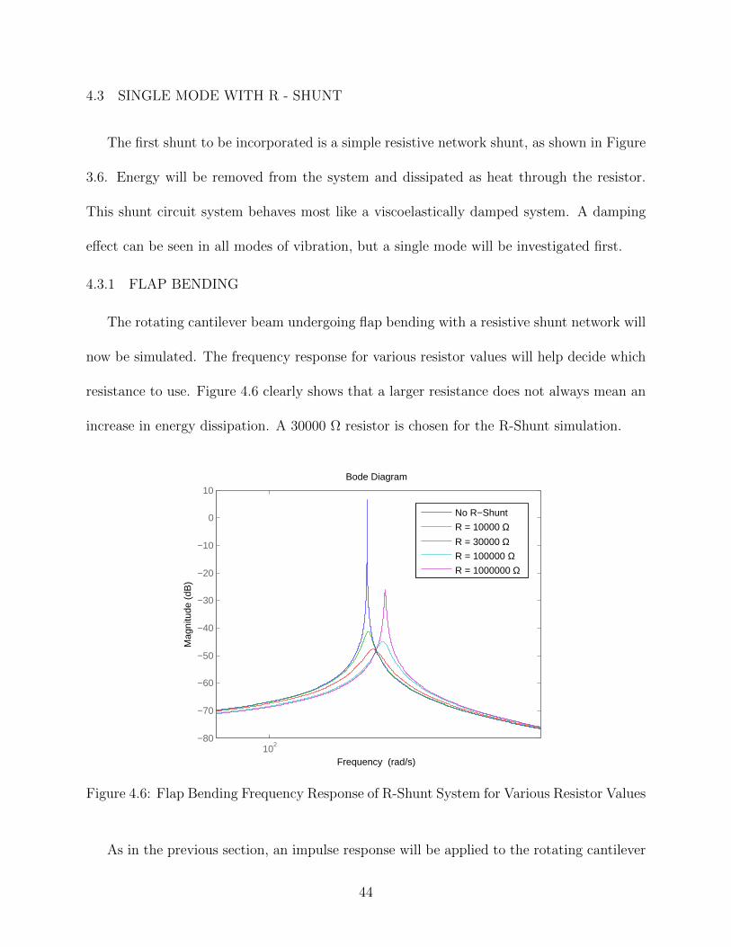
4.3 SINGLE MODE WITH R - SHUNT
The first shunt to be incorporated is a simple resistive network shunt, as shown in Figure
3.6. Energy will be removed from the system and dissipated as heat through the resistor.
This shunt circuit system behaves most like a viscoelastically damped system. A damping
effect can be seen in all modes of vibration, but a single mode will be investigated first.
4.3.1 FLAP BENDING
The rotating cantilever beam undergoing flap bending with a resistive shunt network will
now be simulated. The frequency response for various resistor values will help decide which
resistance to use. Figure 4.6 clearly shows that a larger resistance does not always mean an
increase in energy dissipation. A 30000 Ω resistor is chosen for the R-Shunt simulation.
102−80
−70
−60
−50
−40
−30
−20
−10
0
10
Mag
nitu
de (
dB)
Bode Diagram
Frequency (rad/s)
No R−Shunt
R = 10000 ΩR = 30000 ΩR = 100000 ΩR = 1000000 Ω
Figure 4.6: Flap Bending Frequency Response of R-Shunt System for Various Resistor Values
As in the previous section, an impulse response will be applied to the rotating cantilever
44
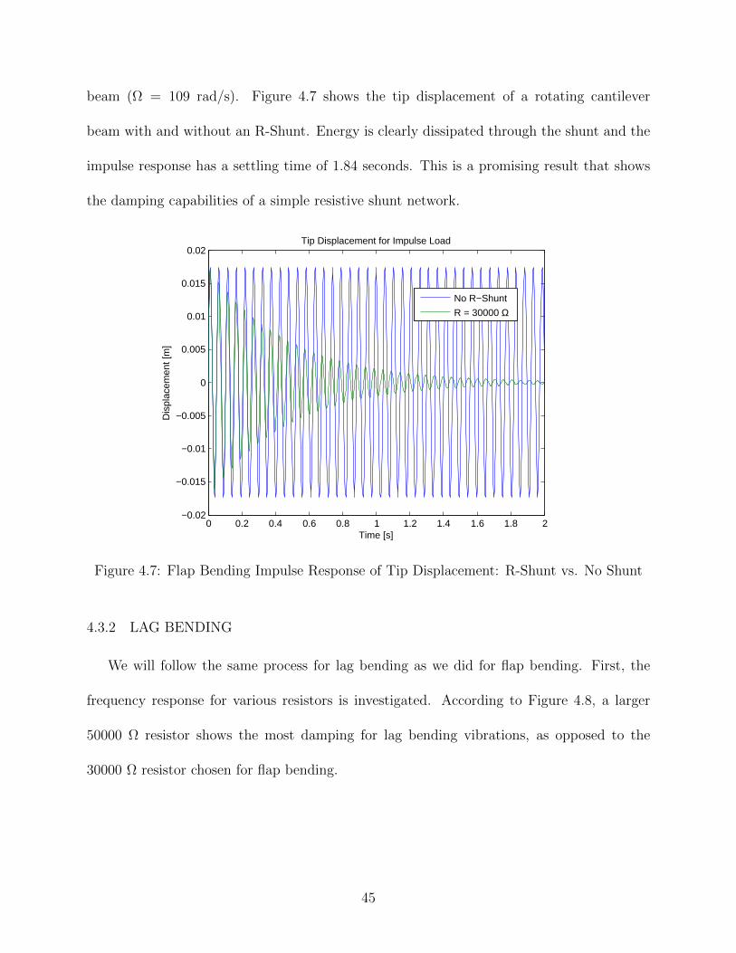
beam (Ω = 109 rad/s). Figure 4.7 shows the tip displacement of a rotating cantilever
beam with and without an R-Shunt. Energy is clearly dissipated through the shunt and the
impulse response has a settling time of 1.84 seconds. This is a promising result that shows
the damping capabilities of a simple resistive shunt network.
0 0.2 0.4 0.6 0.8 1 1.2 1.4 1.6 1.8 2−0.02
−0.015
−0.01
−0.005
0
0.005
0.01
0.015
0.02Tip Displacement for Impulse Load
Time [s]
Dis
plac
emen
t [m
]
No R−Shunt
R = 30000 Ω
Figure 4.7: Flap Bending Impulse Response of Tip Displacement: R-Shunt vs. No Shunt
4.3.2 LAG BENDING
We will follow the same process for lag bending as we did for flap bending. First, the
frequency response for various resistors is investigated. According to Figure 4.8, a larger
50000 Ω resistor shows the most damping for lag bending vibrations, as opposed to the
30000 Ω resistor chosen for flap bending.
45
102−70
−60
−50
−40
−30
−20
−10
0
10
20
Mag
nitu
de (
dB)
Bode Diagram
Frequency (rad/s)
No R−Shunt
R = 30000 ΩR = 50000 ΩR = 100000 ΩR = 1000000 Ω
Figure 4.8: Lag Bending Frequency Response of R-Shunt System for Various Resistor Values
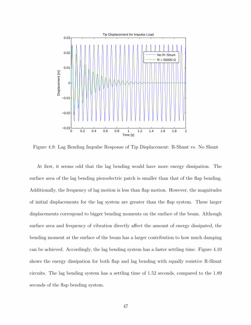
The impulse response for tip displacement under lag motion follows. Figure 4.9 shows
the energy dissipation of the resistive shunt. The R-Shunt system has a settling time of 1.24
seconds.
46
0 0.2 0.4 0.6 0.8 1 1.2 1.4 1.6 1.8 2−0.03
−0.02
−0.01
0
0.01
0.02
0.03Tip Displacement for Impulse Load
Time [s]
Dis
plac
emen
t [m
]
No R−Shunt
R = 50000 Ω
Figure 4.9: Lag Bending Impulse Response of Tip Displacement: R-Shunt vs. No Shunt
At first, it seems odd that the lag bending would have more energy dissipation. The
surface area of the lag bending piezoelectric patch is smaller than that of the flap bending.
Additionally, the frequency of lag motion is less than flap motion. However, the magnitudes
of initial displacements for the lag system are greater than the flap system. These larger
displacements correspond to bigger bending moments on the surface of the beam. Although
surface area and frequency of vibration directly affect the amount of energy dissipated, the
bending moment at the surface of the beam has a larger contribution to how much damping
can be achieved. Accordingly, the lag bending system has a faster settling time. Figure 4.10
shows the energy dissipation for both flap and lag bending with equally resistive R-Shunt
circuits. The lag bending system has a settling time of 1.52 seconds, compared to the 1.89
seconds of the flap bending system.
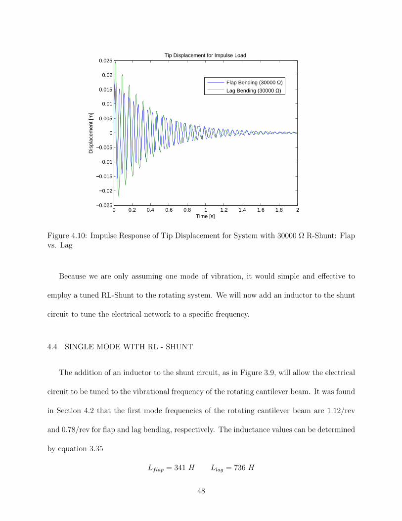
47
0 0.2 0.4 0.6 0.8 1 1.2 1.4 1.6 1.8 2−0.025
−0.02
−0.015
−0.01
−0.005
0
0.005
0.01
0.015
0.02
0.025Tip Displacement for Impulse Load
Time [s]
Dis
plac
emen
t [m
]
Flap Bending (30000 Ω)
Lag Bending (30000 Ω)
Figure 4.10: Impulse Response of Tip Displacement for System with 30000 Ω R-Shunt: Flapvs. Lag
Because we are only assuming one mode of vibration, it would simple and effective to
employ a tuned RL-Shunt to the rotating system. We will now add an inductor to the shunt
circuit to tune the electrical network to a specific frequency.
4.4 SINGLE MODE WITH RL - SHUNT
The addition of an inductor to the shunt circuit, as in Figure 3.9, will allow the electrical
circuit to be tuned to the vibrational frequency of the rotating cantilever beam. It was found
in Section 4.2 that the first mode frequencies of the rotating cantilever beam are 1.12/rev
and 0.78/rev for flap and lag bending, respectively. The inductance values can be determined
by equation 3.35
Lflap = 341 H Llag = 736 H
48
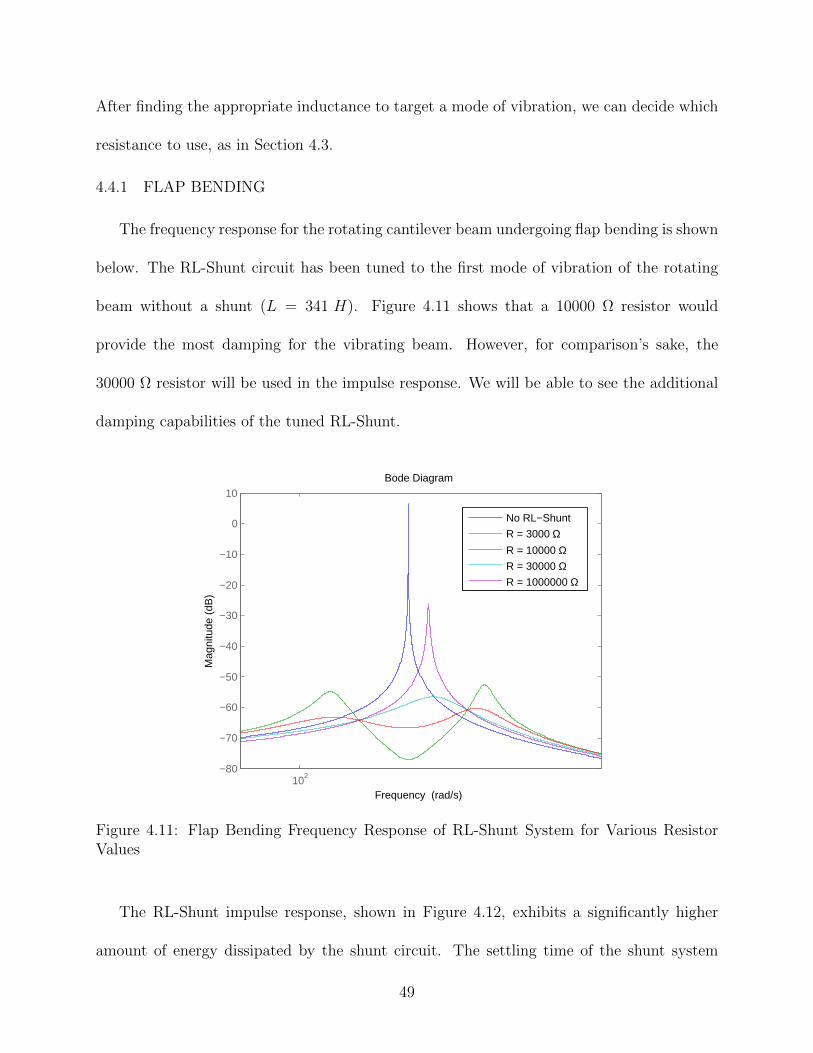
After finding the appropriate inductance to target a mode of vibration, we can decide which
resistance to use, as in Section 4.3.
4.4.1 FLAP BENDING
The frequency response for the rotating cantilever beam undergoing flap bending is shown
below. The RL-Shunt circuit has been tuned to the first mode of vibration of the rotating
beam without a shunt (L = 341 H). Figure 4.11 shows that a 10000 Ω resistor would
provide the most damping for the vibrating beam. However, for comparison’s sake, the
30000 Ω resistor will be used in the impulse response. We will be able to see the additional
damping capabilities of the tuned RL-Shunt.
102−80
−70
−60
−50
−40
−30
−20
−10
0
10
Mag
nitu
de (
dB)
Bode Diagram
Frequency (rad/s)
No RL−Shunt
R = 3000 ΩR = 10000 ΩR = 30000 ΩR = 1000000 Ω
Figure 4.11: Flap Bending Frequency Response of RL-Shunt System for Various ResistorValues
The RL-Shunt impulse response, shown in Figure 4.12, exhibits a significantly higher
amount of energy dissipated by the shunt circuit. The settling time of the shunt system
49
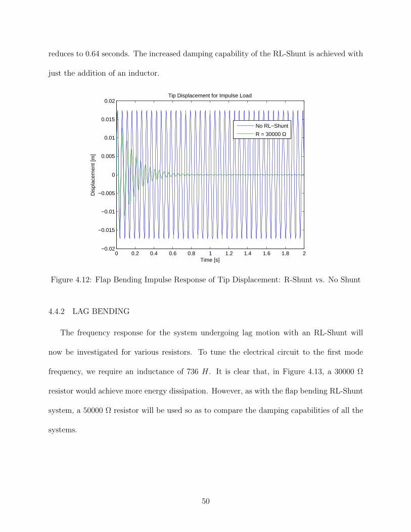
reduces to 0.64 seconds. The increased damping capability of the RL-Shunt is achieved with
just the addition of an inductor.
0 0.2 0.4 0.6 0.8 1 1.2 1.4 1.6 1.8 2−0.02
−0.015
−0.01
−0.005
0
0.005
0.01
0.015
0.02Tip Displacement for Impulse Load
Time [s]
Dis
plac
emen
t [m
]
No RL−Shunt
R = 30000 Ω
Figure 4.12: Flap Bending Impulse Response of Tip Displacement: R-Shunt vs. No Shunt
4.4.2 LAG BENDING
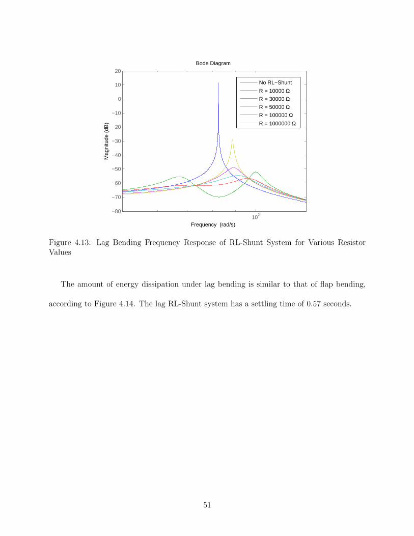
The frequency response for the system undergoing lag motion with an RL-Shunt will
now be investigated for various resistors. To tune the electrical circuit to the first mode
frequency, we require an inductance of 736 H. It is clear that, in Figure 4.13, a 30000 Ω
resistor would achieve more energy dissipation. However, as with the flap bending RL-Shunt
system, a 50000 Ω resistor will be used so as to compare the damping capabilities of all the
systems.
50
102−80
−70
−60
−50
−40
−30
−20
−10
0
10
20
Mag
nitu
de (
dB)
Bode Diagram
Frequency (rad/s)
No RL−Shunt
R = 10000 ΩR = 30000 ΩR = 50000 ΩR = 100000 ΩR = 1000000 Ω
Figure 4.13: Lag Bending Frequency Response of RL-Shunt System for Various ResistorValues
The amount of energy dissipation under lag bending is similar to that of flap bending,
according to Figure 4.14. The lag RL-Shunt system has a settling time of 0.57 seconds.
51
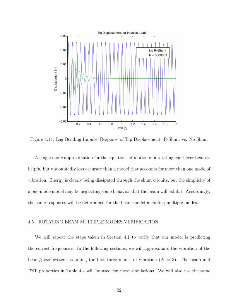
0 0.2 0.4 0.6 0.8 1 1.2 1.4 1.6 1.8 2−0.03
−0.02
−0.01
0
0.01
0.02
0.03Tip Displacement for Impulse Load
Time [s]
Dis
plac
emen
t [m
]
No R−Shunt
R = 50000 Ω
Figure 4.14: Lag Bending Impulse Response of Tip Displacement: R-Shunt vs. No Shunt
A single mode approximation for the equations of motion of a rotating cantilever beam is
helpful but undoubtedly less accurate than a model that accounts for more than one mode of
vibration. Energy is clearly being dissipated through the shunt circuits, but the simplicity of
a one-mode model may be neglecting some behavior that the beam will exhibit. Accordingly,
the same responses will be determined for the beam model including multiple modes.
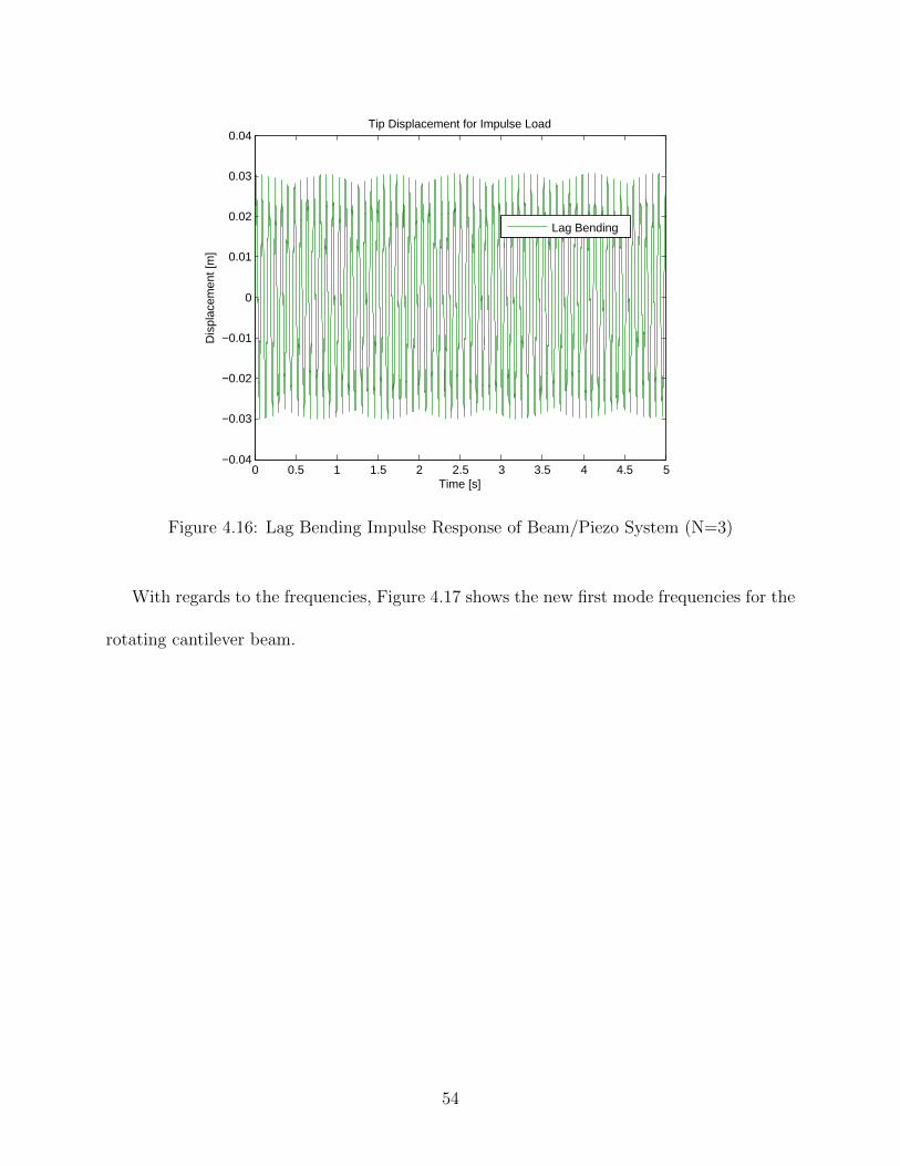
4.5 ROTATING BEAM MULTIPLE MODES VERIFICATION
We will repeat the steps taken in Section 4.1 to verify that our model is predicting
the correct frequencies. In the following sections, we will approximate the vibration of the
beam/piezo system assuming the first three modes of vibration (N = 3). The beam and
PZT properties in Table 4.4 will be used for these simulations. We will also use the same
52
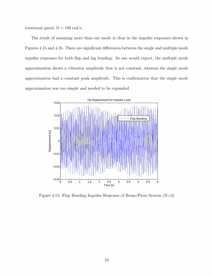
rotational speed, Ω = 109 rad/s.
The result of assuming more than one mode is clear in the impulse responses shown in
Figures 4.15 and 4.16. There are significant differences between the single and multiple mode
impulse responses for both flap and lag bending. As one would expect, the multiple mode
approximation shows a vibration amplitude that is not constant, whereas the single mode
approximation had a constant peak amplitude. This is confirmation that the single mode
approximation was too simple and needed to be expanded.
0 0.5 1 1.5 2 2.5 3 3.5 4 4.5 5−0.03
−0.02
−0.01
0
0.01
0.02
0.03Tip Displacement for Impulse Load
Time [s]
Dis
plac
emen
t [m
]
Flap Bending
Figure 4.15: Flap Bending Impulse Response of Beam/Piezo System (N=3)
53
0 0.5 1 1.5 2 2.5 3 3.5 4 4.5 5−0.04
−0.03
−0.02
−0.01
0
0.01
0.02
0.03
0.04Tip Displacement for Impulse Load
Time [s]
Dis
plac
emen
t [m
]
Lag Bending
Figure 4.16: Lag Bending Impulse Response of Beam/Piezo System (N=3)
With regards to the frequencies, Figure 4.17 shows the new first mode frequencies for the
rotating cantilever beam.
54
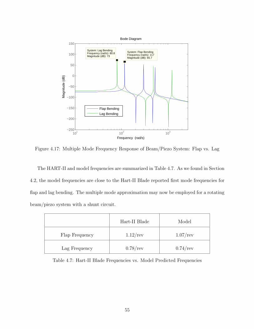
Bode Diagram
Frequency (rad/s)101 102 103
−250
−200
−150
−100
−50
0
50
100
150
System: Lag BendingFrequency (rad/s): 80.8Magnitude (dB): 73
Mag
nitu
de (
dB)
System: Flap Bending Frequency (rad/s): 117Magnitude (dB): 65.7
Flap Bending
Lag Bending
Figure 4.17: Multiple Mode Frequency Response of Beam/Piezo System: Flap vs. Lag
The HART-II and model frequencies are summarized in Table 4.7. As we found in Section
4.2, the model frequencies are close to the Hart-II Blade reported first mode frequencies for
flap and lag bending. The multiple mode approximation may now be employed for a rotating
beam/piezo system with a shunt circuit.
Hart-II Blade Model
Flap Frequency 1.12/rev 1.07/rev
Lag Frequency 0.78/rev 0.74/rev
Table 4.7: Hart-II Blade Frequencies vs. Model Predicted Frequencies
55
4.6 MULTIPLE MODES WITH R-SHUNT
Once again, a simple resistive shunt circuit, as in Figure 3.6, will added to the rotating
beam/piezo system. The advantage to this method, especially for multiple mode approxima-
tions, is that there will be energy dissipation no matter what vibration frequency the beam
is exhibiting. However, choosing the optimal resistor becomes more difficult when multiple
modes are present. The resistor that most dampens the first mode may not be as effective
for the second or third mode. Accordingly, it is ideal to find the dominant mode and choose
the resistor according to that mode’s frequency response.
4.6.1 FLAP BENDING
The frequency response will help us decide which resistance to use for optimal damping
of flap bending vibrations, and each of the three modes will be examined separately. The
change in resistor affects the damping potential for all three modes, as shown in Figure
4.18. It is not very surprising that the first mode frequency response reacts to changes
in resistance similarly to the single mode approximation in Figure 4.6. It appears that a
30000 Ω resistor would achieve the most energy dissipation when the beam vibrates at the
first mode frequency. However, the 15000 Ω resistor shows more of a decrease in vibration
amplitude for both the second and third modes. The system will be simulated for both
resistors to compare the damping capability.
56
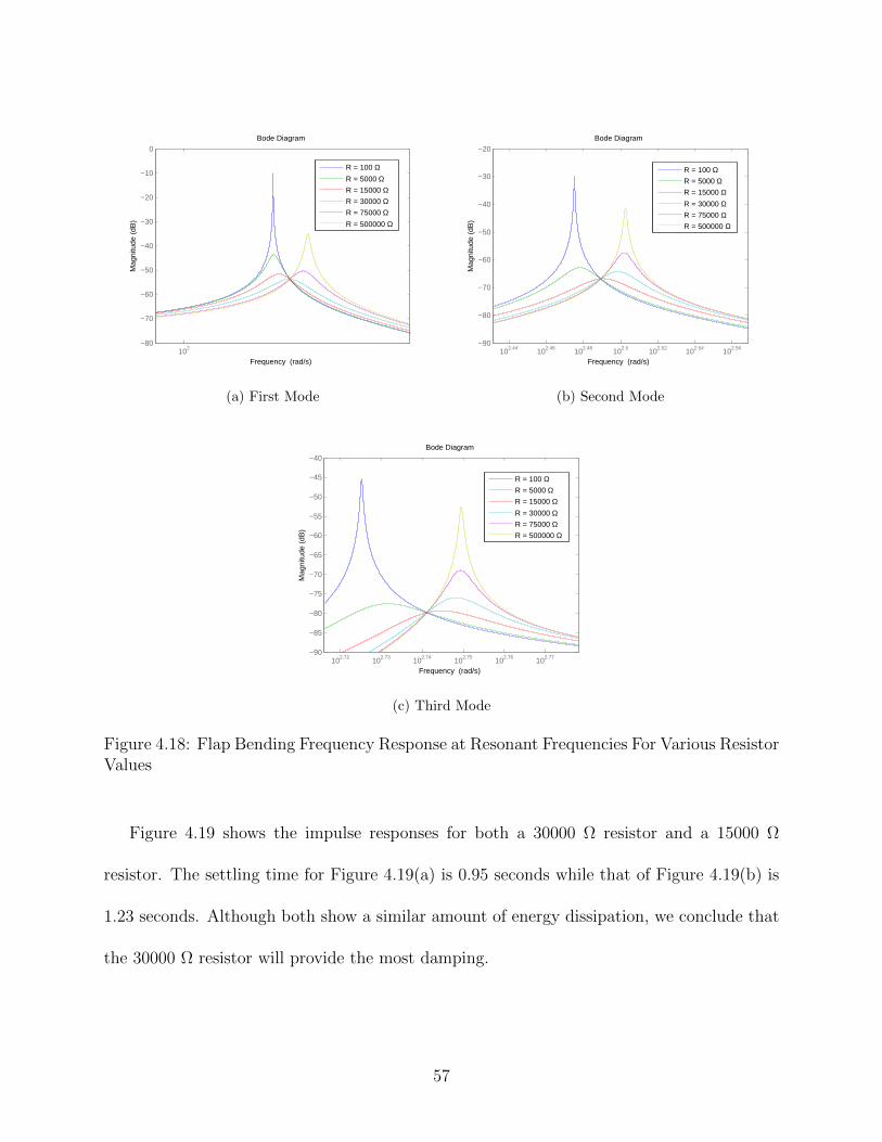
Bode Diagram
Frequency (rad/s)102
−80
−70
−60
−50
−40
−30
−20
−10
0
Mag
nitu
de (
dB)
R = 100 ΩR = 5000 ΩR = 15000 ΩR = 30000 ΩR = 75000 ΩR = 500000 Ω
(a) First Mode
Bode Diagram
Frequency (rad/s)102.44 102.46 102.48 102.5 102.52 102.54 102.56
−90
−80
−70
−60
−50
−40
−30
−20
Mag
nitu
de (
dB)
R = 100 ΩR = 5000 ΩR = 15000 ΩR = 30000 ΩR = 75000 ΩR = 500000 Ω
(b) Second Mode
Bode Diagram
Frequency (rad/s)102.72 102.73 102.74 102.75 102.76 102.77
−90
−85
−80
−75
−70
−65
−60
−55
−50
−45
−40
Mag
nitu
de (
dB)
R = 100 ΩR = 5000 ΩR = 15000 ΩR = 30000 ΩR = 75000 ΩR = 500000 Ω
(c) Third Mode
Figure 4.18: Flap Bending Frequency Response at Resonant Frequencies For Various ResistorValues
Figure 4.19 shows the impulse responses for both a 30000 Ω resistor and a 15000 Ω
resistor. The settling time for Figure 4.19(a) is 0.95 seconds while that of Figure 4.19(b) is
1.23 seconds. Although both show a similar amount of energy dissipation, we conclude that
the 30000 Ω resistor will provide the most damping.
57
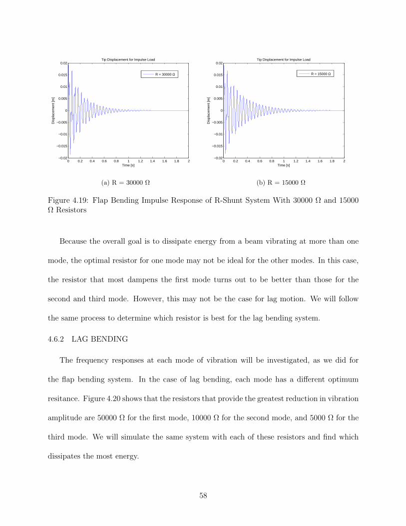
0 0.2 0.4 0.6 0.8 1 1.2 1.4 1.6 1.8 2−0.02
−0.015
−0.01
−0.005
0
0.005
0.01
0.015
0.02Tip Displacement for Impulse Load
Time [s]
Dis
plac
emen
t [m
]
R = 30000 Ω
(a) R = 30000 Ω
0 0.2 0.4 0.6 0.8 1 1.2 1.4 1.6 1.8 2−0.02
−0.015
−0.01
−0.005
0
0.005
0.01
0.015
0.02Tip Displacement for Impulse Load
Time [s]
Dis
plac
emen
t [m
]
R = 15000 Ω
(b) R = 15000 Ω
Figure 4.19: Flap Bending Impulse Response of R-Shunt System With 30000 Ω and 15000Ω Resistors
Because the overall goal is to dissipate energy from a beam vibrating at more than one
mode, the optimal resistor for one mode may not be ideal for the other modes. In this case,
the resistor that most dampens the first mode turns out to be better than those for the
second and third mode. However, this may not be the case for lag motion. We will follow
the same process to determine which resistor is best for the lag bending system.
4.6.2 LAG BENDING
The frequency responses at each mode of vibration will be investigated, as we did for
the flap bending system. In the case of lag bending, each mode has a different optimum
resitance. Figure 4.20 shows that the resistors that provide the greatest reduction in vibration
amplitude are 50000 Ω for the first mode, 10000 Ω for the second mode, and 5000 Ω for the
third mode. We will simulate the same system with each of these resistors and find which
dissipates the most energy.
58
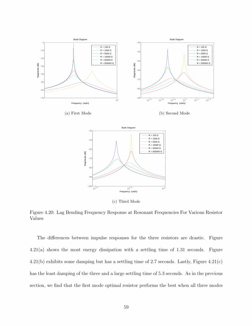
Bode Diagram
Frequency (rad/s)102
−70
−60
−50
−40
−30
−20
−10
0
Mag
nitu
de (
dB)
R = 100 ΩR = 1000 ΩR = 5000 ΩR = 10000 ΩR = 50000 ΩR = 500000 Ω
(a) First Mode
102.67 102.68 102.69 102.7 102.71 102.72−90
−80
−70
−60
−50
−40
−30
Mag
nitu
de (
dB)
Bode Diagram
Frequency (rad/s)
R = 100 ΩR = 1000 ΩR = 5000 ΩR = 10000 ΩR = 50000 ΩR = 500000 Ω
(b) Second Mode
Bode Diagram
Frequency (rad/s)103.08 103.09 103.1
−100
−90
−80
−70
−60
−50
−40
Mag
nitu
de (
dB)
R = 100 ΩR = 1000 ΩR = 5000 ΩR = 10000 ΩR = 50000 ΩR = 500000 Ω
(c) Third Mode
Figure 4.20: Lag Bending Frequency Response at Resonant Frequencies For Various ResistorValues
The differences between impulse responses for the three resistors are drastic. Figure
4.21(a) shows the most energy dissipation with a settling time of 1.31 seconds. Figure
4.21(b) exhibits some damping but has a settling time of 2.7 seconds. Lastly, Figure 4.21(c)
has the least damping of the three and a large settling time of 5.3 seconds. As in the previous
section, we find that the first mode optimal resistor performs the best when all three modes
59
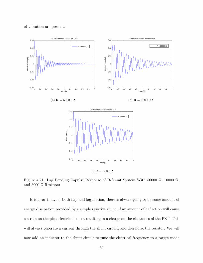
of vibration are present.
0 0.2 0.4 0.6 0.8 1 1.2 1.4 1.6 1.8 2−0.03
−0.02
−0.01
0
0.01
0.02
0.03Tip Displacement for Impulse Load
Time [s]
Dis
plac
emen
t [m
]
R = 50000 Ω
(a) R = 50000 Ω
0 0.2 0.4 0.6 0.8 1 1.2 1.4 1.6 1.8 2−0.03
−0.02
−0.01
0
0.01
0.02
0.03Tip Displacement for Impulse Load
Time [s]
Dis
plac
emen
t [m
]
R = 10000 Ω
(b) R = 10000 Ω
0 0.2 0.4 0.6 0.8 1 1.2 1.4 1.6 1.8 2−0.03
−0.02
−0.01
0
0.01
0.02
0.03Tip Displacement for Impulse Load
Time [s]
Dis
plac
emen
t [m
]
R = 5000 Ω
(c) R = 5000 Ω
Figure 4.21: Lag Bending Impulse Response of R-Shunt System With 50000 Ω, 10000 Ω,and 5000 Ω Resistors
It is clear that, for both flap and lag motion, there is always going to be some amount of
energy dissipation provided by a simple resistive shunt. Any amount of deflection will cause
a strain on the piezoelectric element resulting in a charge on the electrodes of the PZT. This
will always generate a current through the shunt circuit, and therefore, the resistor. We will
now add an inductor to the shunt circuit to tune the electrical frequency to a target mode
60
frequency.
4.7 MULTIPLE MODES WITH RL-SHUNT
As previously discussed, it is advantageous to include an inductor in the shunt circuit if
we want to target a specific mode or frequency of vibration for energy dissipation. For the
single mode simulations, the RL-Shunt system provided significantly more damping than the
purely resistive shunt circuit. This is because there were no other modes present to interfere
with the mechanical vibration frequency. Because we assumed that the beam vibrated at
or near a single frequency, the shunt circuit could be tuned such that it would allow the
maximum amount of current to flow through it. If multiple modes are introduced to the
simulation, we cannot assume that the shunt circuit will always remove energy from the
system. This concept will be investigated for both flap and lag motion.
4.7.1 FLAP BENDING TUNED TO FIRST MODE
The first mode frequency will be targeted in this simulation. Therefore, the frequency we
will tune the RL-Shunt to is 117 rad/s. The inductance required to tune the circuit to that
frequency is 365 H. It is clear that, in Figure 4.22(a), the tuning of the RL-Shunt to the
first mode frequency shifts the frequencies of the second and third modes. Figure 4.22(b)
is a close up view of the first mode frequency range. As before, an increase in resistance
reduces vibration amplitude up to a certain point. The 25000 Ω resistor corresponds to the
most energy dissipation in the first mode frequency range. We will now simulate the impulse
response for the system with a 25000 Ω resistor.
61
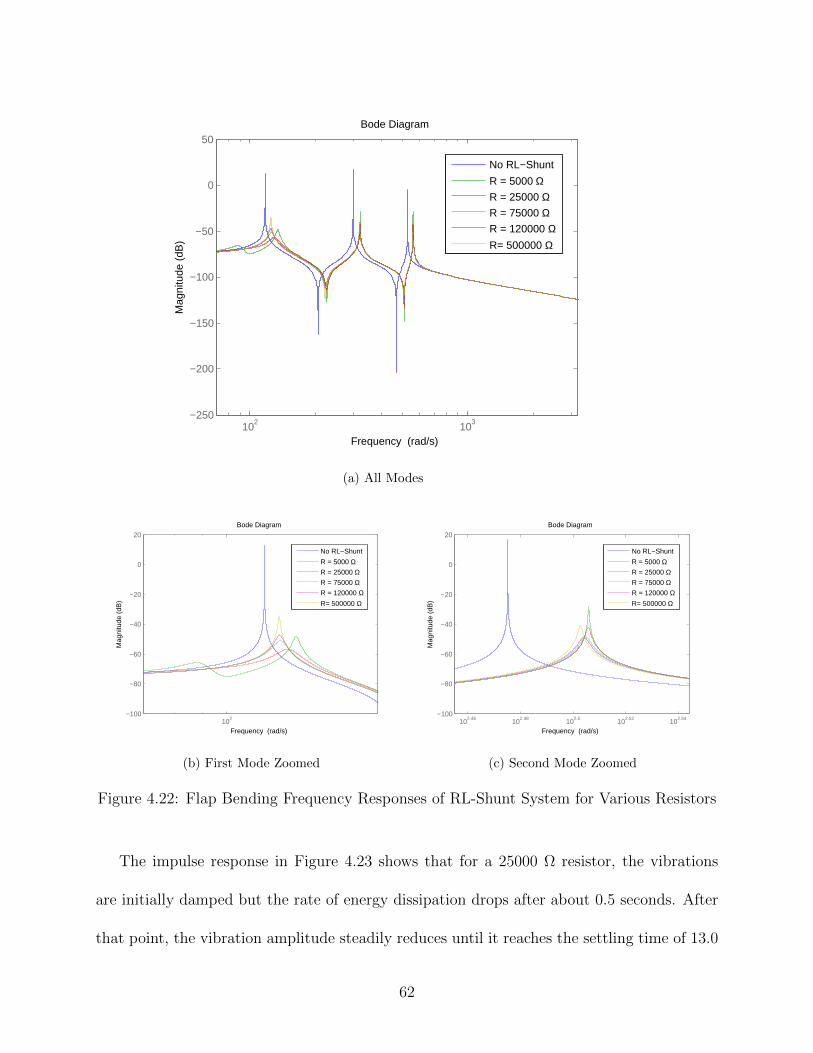
Bode Diagram
Frequency (rad/s)102 103
−250
−200
−150
−100
−50
0
50
Mag
nitu
de (
dB)
No RL−Shunt
R = 5000 ΩR = 25000 ΩR = 75000 ΩR = 120000 ΩR= 500000 Ω
(a) All Modes
Bode Diagram
Frequency (rad/s)102
−100
−80
−60
−40
−20
0
20
Mag
nitu
de (
dB)
No RL−Shunt
R = 5000 ΩR = 25000 ΩR = 75000 ΩR = 120000 ΩR= 500000 Ω
(b) First Mode Zoomed
Bode Diagram
Frequency (rad/s)102.46 102.48 102.5 102.52 102.54
−100
−80
−60
−40
−20
0
20
Mag
nitu
de (
dB)
No RL−Shunt
R = 5000 ΩR = 25000 ΩR = 75000 ΩR = 120000 ΩR= 500000 Ω
(c) Second Mode Zoomed
Figure 4.22: Flap Bending Frequency Responses of RL-Shunt System for Various Resistors
The impulse response in Figure 4.23 shows that for a 25000 Ω resistor, the vibrations
are initially damped but the rate of energy dissipation drops after about 0.5 seconds. After
that point, the vibration amplitude steadily reduces until it reaches the settling time of 13.0
62
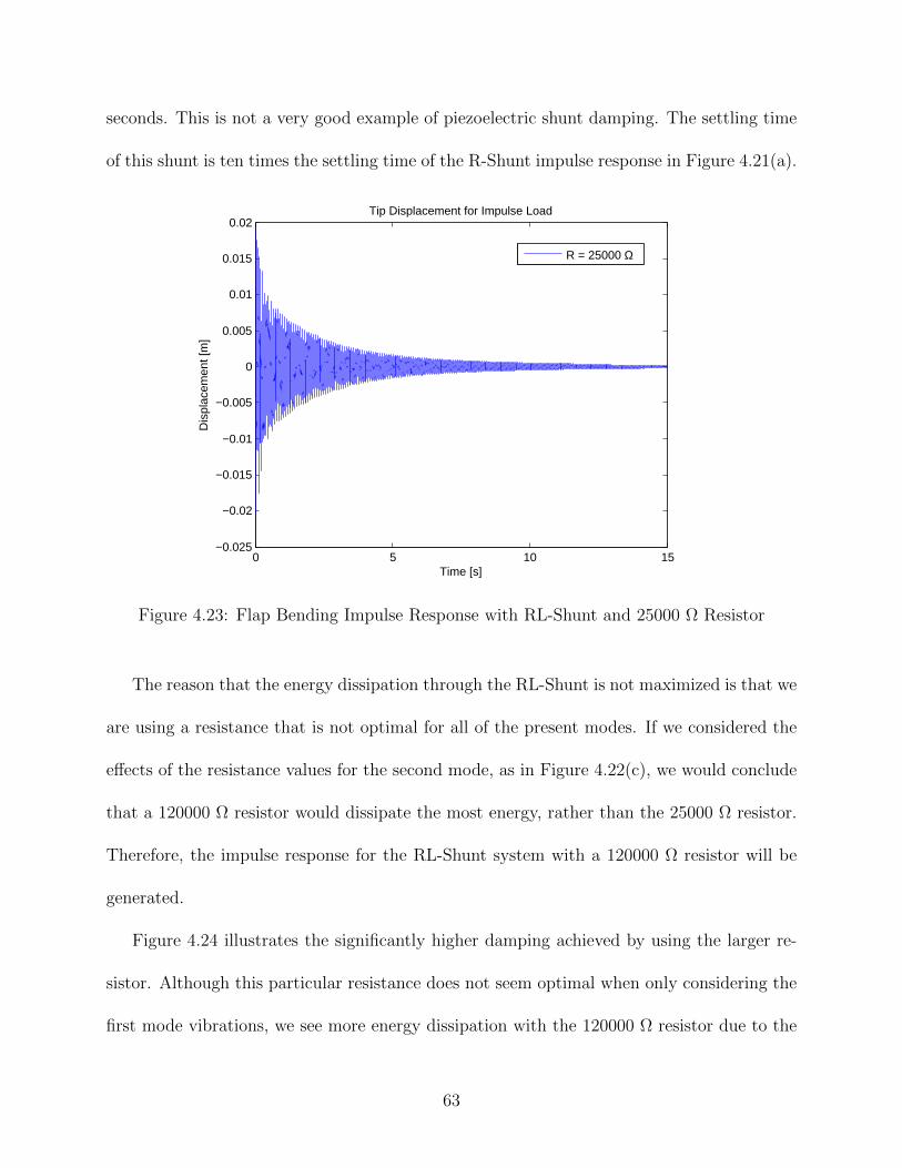
seconds. This is not a very good example of piezoelectric shunt damping. The settling time
of this shunt is ten times the settling time of the R-Shunt impulse response in Figure 4.21(a).
0 5 10 15−0.025
−0.02
−0.015
−0.01
−0.005
0
0.005
0.01
0.015
0.02Tip Displacement for Impulse Load
Time [s]
Dis
plac
emen
t [m
]
R = 25000 Ω
Figure 4.23: Flap Bending Impulse Response with RL-Shunt and 25000 Ω Resistor
The reason that the energy dissipation through the RL-Shunt is not maximized is that we
are using a resistance that is not optimal for all of the present modes. If we considered the
effects of the resistance values for the second mode, as in Figure 4.22(c), we would conclude
that a 120000 Ω resistor would dissipate the most energy, rather than the 25000 Ω resistor.
Therefore, the impulse response for the RL-Shunt system with a 120000 Ω resistor will be
generated.
Figure 4.24 illustrates the significantly higher damping achieved by using the larger re-
sistor. Although this particular resistance does not seem optimal when only considering the
first mode vibrations, we see more energy dissipation with the 120000 Ω resistor due to the
63
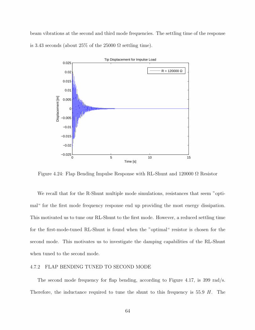
beam vibrations at the second and third mode frequencies. The settling time of the response
is 3.43 seconds (about 25% of the 25000 Ω settling time).
0 5 10 15−0.025
−0.02
−0.015
−0.01
−0.005
0
0.005
0.01
0.015
0.02
0.025Tip Displacement for Impulse Load
Time [s]
Dis
plac
emen
t [m
]
R = 120000 Ω
Figure 4.24: Flap Bending Impulse Response with RL-Shunt and 120000 Ω Resistor
We recall that for the R-Shunt multiple mode simulations, resistances that seem ”opti-
mal“ for the first mode frequency response end up providing the most energy dissipation.
This motivated us to tune our RL-Shunt to the first mode. However, a reduced settling time
for the first-mode-tuned RL-Shunt is found when the ”optimal“ resistor is chosen for the
second mode. This motivates us to investigate the damping capabilities of the RL-Shunt
when tuned to the second mode.
4.7.2 FLAP BENDING TUNED TO SECOND MODE
The second mode frequency for flap bending, according to Figure 4.17, is 399 rad/s.
Therefore, the inductance required to tune the shunt to this frequency is 55.9 H. The
64
frequency response for various resistors is found in Figure 4.25. The frequency responses
around the second mode in Figure 4.25(c) are similar to those of the first mode in Figure
4.22(b). The resistor that reduces the vibration amplitude at the second mode is 10000 Ω.
However, the corresponding resistor for the first mode is 30000 Ω.
65
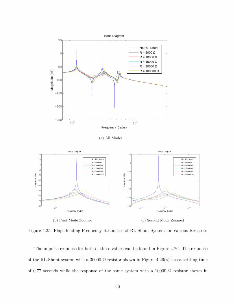
102 103−250
−200
−150
−100
−50
0
50
Mag
nitu
de (
dB)
Bode Diagram
Frequency (rad/s)
No RL−Shunt
R = 5000 ΩR = 10000 ΩR = 15000 ΩR = 30000 ΩR = 100000 Ω
(a) All Modes
102−80
−70
−60
−50
−40
−30
−20
−10
0
10
20
Mag
nitu
de (
dB)
Bode Diagram
Frequency (rad/s)
No RL−Shunt
R = 5000 ΩR = 10000 ΩR = 15000 ΩR = 30000 ΩR = 100000 Ω
(b) First Mode Zoomed
Bode Diagram
Frequency (rad/s)102.4 102.5 102.6
−100
−80
−60
−40
−20
0
20
Mag
nitu
de (
dB)
No RL−Shunt
R = 5000 ΩR = 10000 ΩR = 15000 ΩR = 30000 ΩR = 100000 Ω
(c) Second Mode Zoomed
Figure 4.25: Flap Bending Frequency Responses of RL-Shunt System for Various Resistors
The impulse response for both of these values can be found in Figure 4.26. The response
of the RL-Shunt system with a 30000 Ω resistor shown in Figure 4.26(a) has a settling time
of 0.77 seconds while the response of the same system with a 10000 Ω resistor shown in
66
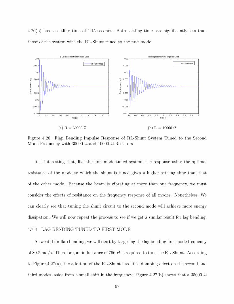
4.26(b) has a settling time of 1.15 seconds. Both settling times are significantly less than
those of the system with the RL-Shunt tuned to the first mode.
0 0.2 0.4 0.6 0.8 1 1.2 1.4 1.6 1.8 2−0.02
−0.015
−0.01
−0.005
0
0.005
0.01
0.015
0.02Tip Displacement for Impulse Load
Time [s]
Dis
plac
emen
t [m
]
R = 30000 Ω
(a) R = 30000 Ω
0 0.2 0.4 0.6 0.8 1 1.2 1.4 1.6 1.8 2−0.02
−0.015
−0.01
−0.005
0
0.005
0.01
0.015
0.02Tip Displacement for Impulse Load
Time [s]D
ispl
acem
ent [
m]
R = 10000 Ω
(b) R = 10000 Ω
Figure 4.26: Flap Bending Impulse Response of RL-Shunt System Tuned to the SecondMode Frequency with 30000 Ω and 10000 Ω Resistors
It is interesting that, like the first mode tuned system, the response using the optimal
resistance of the mode to which the shunt is tuned gives a higher settling time than that
of the other mode. Because the beam is vibrating at more than one frequency, we must
consider the effects of resistance on the frequency response of all modes. Nonetheless, We
can clearly see that tuning the shunt circuit to the second mode will achieve more energy
dissipation. We will now repeat the process to see if we get a similar result for lag bending.
4.7.3 LAG BENDING TUNED TO FIRST MODE
As we did for flap bending, we will start by targeting the lag bending first mode frequency
of 80.8 rad/s. Therefore, an inductance of 766 H is required to tune the RL-Shunt. According
to Figure 4.27(a), the addition of the RL-Shunt has little damping effect on the second and
third modes, aside from a small shift in the frequency. Figure 4.27(b) shows that a 35000 Ω
67
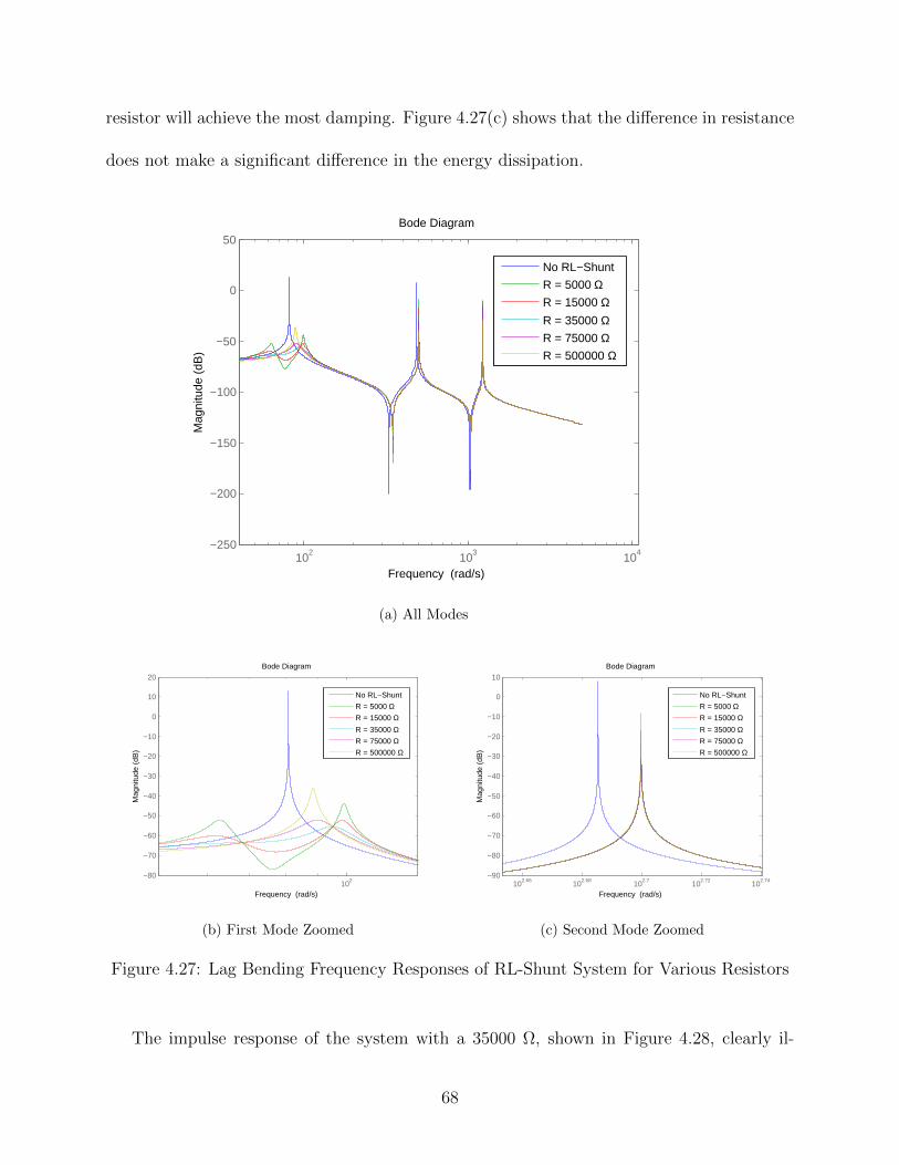
resistor will achieve the most damping. Figure 4.27(c) shows that the difference in resistance
does not make a significant difference in the energy dissipation.
102 103 104−250
−200
−150
−100
−50
0
50
Mag
nitu
de (
dB)
Bode Diagram
Frequency (rad/s)
No RL−Shunt
R = 5000 ΩR = 15000 ΩR = 35000 ΩR = 75000 ΩR = 500000 Ω
(a) All Modes
102−80
−70
−60
−50
−40
−30
−20
−10
0
10
20
Mag
nitu
de (
dB)
Bode Diagram
Frequency (rad/s)
No RL−Shunt
R = 5000 ΩR = 15000 ΩR = 35000 ΩR = 75000 ΩR = 500000 Ω
(b) First Mode Zoomed
102.66 102.68 102.7 102.72 102.74−90
−80
−70
−60
−50
−40
−30
−20
−10
0
10
Mag
nitu
de (
dB)
Bode Diagram
Frequency (rad/s)
No RL−Shunt
R = 5000 ΩR = 15000 ΩR = 35000 ΩR = 75000 ΩR = 500000 Ω
(c) Second Mode Zoomed
Figure 4.27: Lag Bending Frequency Responses of RL-Shunt System for Various Resistors
The impulse response of the system with a 35000 Ω, shown in Figure 4.28, clearly il-
68
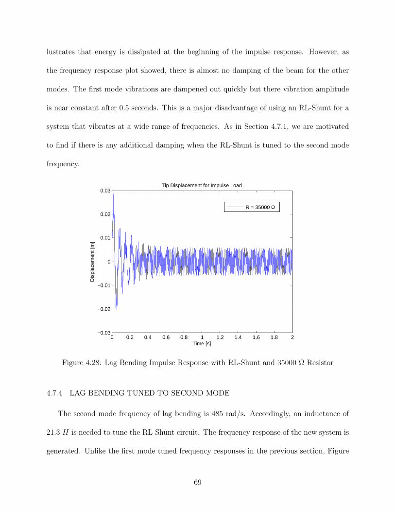
lustrates that energy is dissipated at the beginning of the impulse response. However, as
the frequency response plot showed, there is almost no damping of the beam for the other
modes. The first mode vibrations are dampened out quickly but there vibration amplitude
is near constant after 0.5 seconds. This is a major disadvantage of using an RL-Shunt for a
system that vibrates at a wide range of frequencies. As in Section 4.7.1, we are motivated
to find if there is any additional damping when the RL-Shunt is tuned to the second mode
frequency.
0 0.2 0.4 0.6 0.8 1 1.2 1.4 1.6 1.8 2−0.03
−0.02
−0.01
0
0.01
0.02
0.03Tip Displacement for Impulse Load
Time [s]
Dis
plac
emen
t [m
]
R = 35000 Ω
Figure 4.28: Lag Bending Impulse Response with RL-Shunt and 35000 Ω Resistor
4.7.4 LAG BENDING TUNED TO SECOND MODE
The second mode frequency of lag bending is 485 rad/s. Accordingly, an inductance of
21.3 H is needed to tune the RL-Shunt circuit. The frequency response of the new system is
generated. Unlike the first mode tuned frequency responses in the previous section, Figure
69
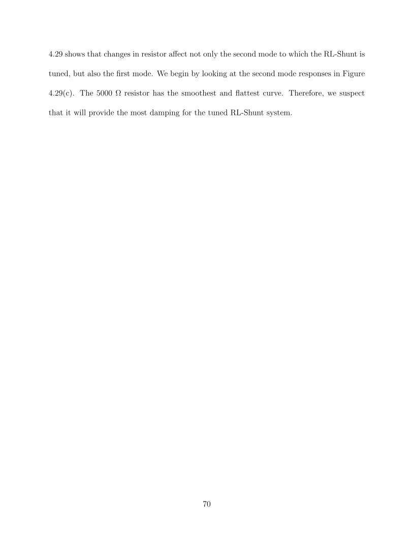
4.29 shows that changes in resistor affect not only the second mode to which the RL-Shunt is
tuned, but also the first mode. We begin by looking at the second mode responses in Figure
4.29(c). The 5000 Ω resistor has the smoothest and flattest curve. Therefore, we suspect
that it will provide the most damping for the tuned RL-Shunt system.
70
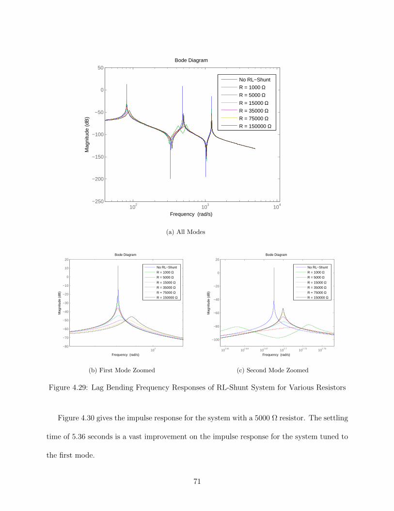
102 103 104−250
−200
−150
−100
−50
0
50
Mag
nitu
de (
dB)
Bode Diagram
Frequency (rad/s)
No RL−Shunt
R = 1000 ΩR = 5000 ΩR = 15000 ΩR = 35000 ΩR = 75000 ΩR = 150000 Ω
(a) All Modes
102−80
−70
−60
−50
−40
−30
−20
−10
0
10
20
Mag
nitu
de (
dB)
Bode Diagram
Frequency (rad/s)
No RL−Shunt
R = 1000 ΩR = 5000 ΩR = 15000 ΩR = 35000 ΩR = 75000 ΩR = 150000 Ω
(b) First Mode Zoomed
102.61 102.64 102.67 102.7 102.73 102.76
−100
−80
−60
−40
−20
0
20
Mag
nitu
de (
dB)
Bode Diagram
Frequency (rad/s)
No RL−Shunt
R = 1000 ΩR = 5000 ΩR = 15000 ΩR = 35000 ΩR = 75000 ΩR = 150000 Ω
(c) Second Mode Zoomed
Figure 4.29: Lag Bending Frequency Responses of RL-Shunt System for Various Resistors
Figure 4.30 gives the impulse response for the system with a 5000 Ω resistor. The settling
time of 5.36 seconds is a vast improvement on the impulse response for the system tuned to
the first mode.
71
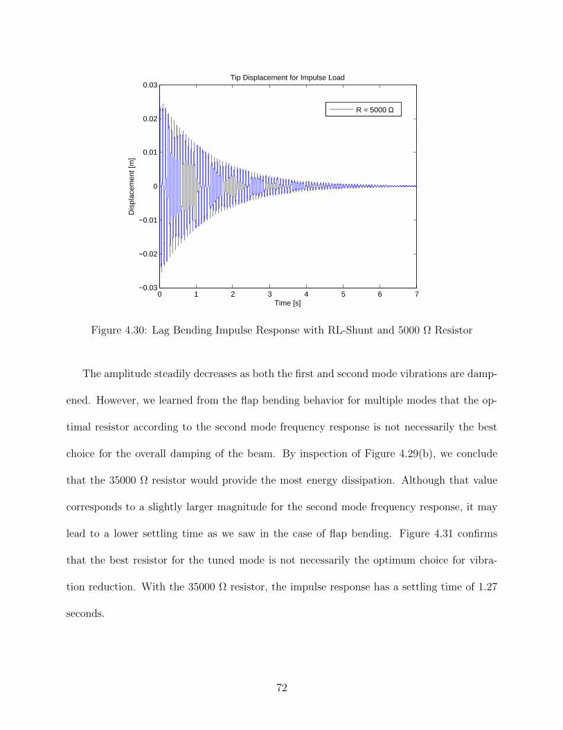
0 1 2 3 4 5 6 7−0.03
−0.02
−0.01
0
0.01
0.02
0.03Tip Displacement for Impulse Load
Time [s]
Dis
plac
emen
t [m
]
R = 5000 Ω
Figure 4.30: Lag Bending Impulse Response with RL-Shunt and 5000 Ω Resistor
The amplitude steadily decreases as both the first and second mode vibrations are damp-
ened. However, we learned from the flap bending behavior for multiple modes that the op-
timal resistor according to the second mode frequency response is not necessarily the best
choice for the overall damping of the beam. By inspection of Figure 4.29(b), we conclude
that the 35000 Ω resistor would provide the most energy dissipation. Although that value
corresponds to a slightly larger magnitude for the second mode frequency response, it may
lead to a lower settling time as we saw in the case of flap bending. Figure 4.31 confirms
that the best resistor for the tuned mode is not necessarily the optimum choice for vibra-
tion reduction. With the 35000 Ω resistor, the impulse response has a settling time of 1.27
seconds.
72
0 1 2 3 4 5 6 7−0.03
−0.02
−0.01
0
0.01
0.02
0.03Tip Displacement for Impulse Load
Time [s]
Dis
plac
emen
t [m
]
R = 35000 Ω
Figure 4.31: Lag Bending Impulse Response with RL-Shunt and 35000 Ω Resistor
This is the case for both flap and lag bending when the shunt circuit is tuned to the
second mode frequency. We have found that energy dissipation is attainable through either
R-Shunt or RL-Shunt circuits for both flap and lag bending motion. As expected, the size of
the resistor directly affects the damping potential of the system. The next chapter presents
a summary and comparison of all the systems we have investigated.
73
CHAPTER 5
DISCUSSION
5.1 SUMMARY OF RESULTS
Chapter 4 explored the energy dissipation capabilities of two different shunt circuits
applied to a rotating cantilever beam undergoing flap or lag bending. Both single-mode
and multi-mode approximations were included which resulted in the investigation thirteen
separate electromechanical systems. Table 5.1 reports the settling times for all thirteen
systems of interest. The type of bending, number of modes, shunt design, and resistor size
are the parameters that define each system.
74
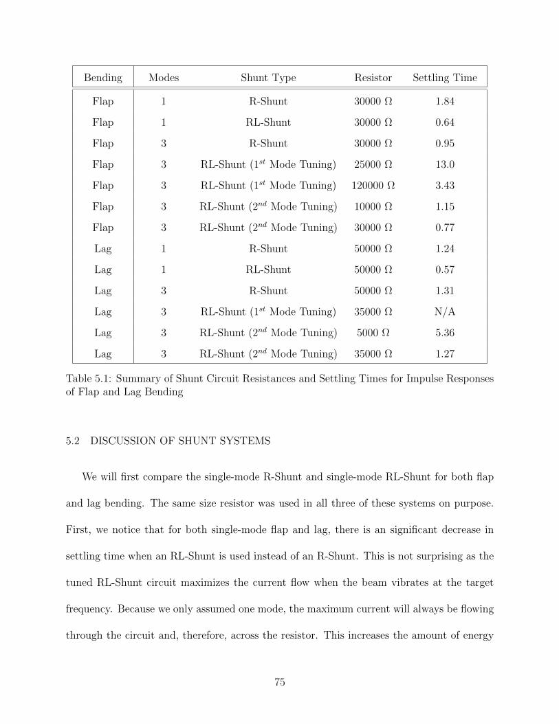
Bending Modes Shunt Type Resistor Settling Time
Flap 1 R-Shunt 30000 Ω 1.84
Flap 1 RL-Shunt 30000 Ω 0.64
Flap 3 R-Shunt 30000 Ω 0.95
Flap 3 RL-Shunt (1st Mode Tuning) 25000 Ω 13.0
Flap 3 RL-Shunt (1st Mode Tuning) 120000 Ω 3.43
Flap 3 RL-Shunt (2nd Mode Tuning) 10000 Ω 1.15
Flap 3 RL-Shunt (2nd Mode Tuning) 30000 Ω 0.77
Lag 1 R-Shunt 50000 Ω 1.24
Lag 1 RL-Shunt 50000 Ω 0.57
Lag 3 R-Shunt 50000 Ω 1.31
Lag 3 RL-Shunt (1st Mode Tuning) 35000 Ω N/A
Lag 3 RL-Shunt (2nd Mode Tuning) 5000 Ω 5.36
Lag 3 RL-Shunt (2nd Mode Tuning) 35000 Ω 1.27
Table 5.1: Summary of Shunt Circuit Resistances and Settling Times for Impulse Responsesof Flap and Lag Bending
5.2 DISCUSSION OF SHUNT SYSTEMS
We will first compare the single-mode R-Shunt and single-mode RL-Shunt for both flap
and lag bending. The same size resistor was used in all three of these systems on purpose.
First, we notice that for both single-mode flap and lag, there is an significant decrease in
settling time when an RL-Shunt is used instead of an R-Shunt. This is not surprising as the
tuned RL-Shunt circuit maximizes the current flow when the beam vibrates at the target
frequency. Because we only assumed one mode, the maximum current will always be flowing
through the circuit and, therefore, across the resistor. This increases the amount of energy
75
dissipated as heat by the resistor, so we see a reduction of settling time of 65% for flap and
54% for lag.
Next, the difference between single-mode and multi-mode R-Shunts for both flap and lag
will be highlighted. Flap bending shows a large reduction in settling time when using three
modes rather than one. The frequency responses in Figure 4.18 show that, although the
30000 Ω resistor is not the best for the second and third modes, it still provides damping
at both modes. The differences between the frequency responses of the optimal resistor and
30000 Ω resistor are quite small for both the second and third modes. Therefore, we see
additional energy dissipation when we expand to three modes.
The difference between single-mode and multi-mode R-Shunts for lag bending, however,
is the opposite of flap bending. When the impulse response is expanded to include three
modes, we see an increase in settling time. Again, we consult the frequency responses of the
three-mode system in Figure 4.20. When resistors for the second and third modes, we notice
a larger separation between the optimal curve and the curve corresponding to the chosen
50000 Ω resistor. This separation results in the increase in settling time.
When comparing the single-mode RL-Shunt to the multi-mode RL-Shunts, we notice an
increase in settling times for both flap and lag bending, regardless of tuning. It has been
emphasized that if a structure is vibrating at a wide range of frequencies, an RL-Shunt circuit
will dissipate less energy than it would if the structure is vibrating at an isolated frequency.
Therefore, it is no surprise that the single-mode RL-Shunts have the lowest settling times of
all the systems. The single-mode approximation, however, is an unrealistic one. It is useful
when learning the fundamental electromechanical behavior of a beam/piezo with a shunt
circuit, but is too simple and does inaccurately describe the system’s behavior. Such is the
76
case for both R-Shunts and RL-Shunts.
The multi-mode RL-Shunts that are tuned to the first mode for flap and lag bending
highlight the inaccuracy of the single-mode approximation. With the optimal resistors for
the single-mode RL-Shunts for both flap and lag, the settling times are found to be 0.64
seconds and 0.57 seconds, respectively. Then the simulations are altered to include three
modes, the RL-Shunts are tuned to the first mode frequencies, and the optimal resistors for
the first mode are selected. At this point, the two models (single and multi mode) are both
tuned to the first mode with the optimal resistor included in the circuit. The only difference,
the number of modes, turns out to have quite an effect on the systems. For flap bending,
the settling time increases about 2000%. The lag bending multi-mode RL-Shunt never even
settles. These contradictory results clearly show the purpose of including multiple modes in
the model.
We found that the flap bending RL-Shunt tuned to the first mode has a settling time
of 13.0 seconds, a rather large value. It was pointed out in Section 4.7 that the optimal
resistor for the first mode frequency response may not necessarily be best for the second
and third modes. After finding a high settling time for the 25000 Ω resistor, we noticed
that the vibrations were quickly dampened at the beginning but slowly decreased after less
than a second. This suggested that the vibrations of another mode were not being reduced.
We looked at the frequency response at the second mode and found that the ideal resistor
near that frequency was 120000 Ω. This value corresponded to a frequency response with
less damping than the 25000 Ω resistor for the first mode frequency. The impulse response
generated for the 120000 Ω resistor showed much more energy dissipation, as the settling
time dropped to 3.43 seconds. The frequency response near the third mode did not change
77
much with varying resistance. Therefore, we only considered the second mode when choosing
an alternative resistance. These results reinforced the notion that the best resistor for an
RL-Shunt is not necessarily the one that shows the most damping at the targeted frequency.
As for lag bending, the RL-Shunt tuned to the first mode was much less effective than
it was for flap bending. The change in resistor affected the vibration reduction at the
beginning of the impulse response, as it did for flap bending. However, after the first mode
was damped out, the vibration amplitude stayed constant, as in Figure 4.28. There was no
settling time for the system because it was, effectively, an undamped oscillating beam. The
frequency response in Figure 4.27(c) shows minimal damping or change in damping with
varying resistance. Therefore, no effort was made to find an optimal resistance because this
RL-Shunt design eventually stops dissipating energy for all of the resistors.
Having discovered that the frequency response of the second mode has a direct effect on
the energy dissipation of both flap and lag RL-Shunts, we decided to tune the RL-Shunt to
the second mode frequency, rather than that of the first mode. We found that the impulse
responses had much smaller settling times when tuned to the second mode. For flap bending,
the optimal resistor in the vicinity of the second mode was 10000 Ω and gave a settling time
of 1.15 seconds. However, from our previous results, we knew that the ideal resistor for the
second mode was not ideal for the first or third. A 30000 Ω resistor was found to provide
more energy dissipation at the first mode frequency. The impulse response in Figure 4.26
shows that the new resistor gives a settling time of 0.77 seconds.
The same process was followed for the lag bending RL-Shunts tuned to the second mode.
Initially, a 5000 Ω resistor was used for the impulse response and the settling time was
5.36 seconds. We adjusted this value, as we did for the flap bending, after looking at the
78
first mode frequency response. The new 35000 Ω resistor lowered the settling time to 1.27
seconds.
It is worth noting that we were able to drastically reduce the settling time of the same
exact beam/piezo system solely by adjusting the electrical components in the shunt circuit.
We reduced the settling time by 12.23 seconds and 4.09 seconds for flap and lag bending,
respectively. It is also important to recognize that the inductances required to tune the
RL-Shunts to the second mode are much smaller than those for the first mode. The 766
H inductor for the first lag mode is unrealistically large compared to the second mode
inductance of 21.3 H. It would be impractical to install a 766 H inductor on a complex
structure like a helicopter rotor.
The results found in Chapter 4 show that energy dissipation of a rotating cantilever
beam is possible through piezoelectric shunt circuits. Variations in electrical components are
strongly related to the damping capabilities of the shunts. For both flap and lag bending, the
second mode tuned RL-Shunts had smaller settling times than the R-Shunts. This is because
the second mode is dominant during the impulse response. The various resistance values used
in the simulations were chosen somewhat arbitrarily. Although we chose an “optimal” resistor
for each system by looking at the frequency response, the true “best case” value for achieving
the most energy dissipation is most likely near our optimal resistance but slightly higher
or lower. The range of whole number resistances was chosen to simplify the comparison of
different systems and to emphasize the effects on the frequency responses. Energy dissipation
shown in the impulse responses in Chapter 4 confirms that passive vibration damping of a
rotating cantilever beam has been achieved through piezoelectric shunt circuits.
79
CHAPTER 6
CONCLUSION
6.1 DAMPING POTENTIAL
Vibration reduction of a rotating cantilever beam by means of a piezoelectric element
connected to a shunt circuit was investigated. First, the mathematical model for a rotating
cantilever beam with a piezoelectric element was developed using the Rayleigh-Ritz method
of assumed modes. The equations of motion were derived for both flap and lag bending. Next,
the equations pertaining to the electrical circuit of both a resistive shunt and a resistive-
inductive shunt were incorporated into the beam/piezo equations of motion. The state
space representation of the electromechanical system was derived to allow the generation of
frequency and impulse responses.
In order to verify our model, the frequency response was found for beam and piezoelectric
parameters from a previous study in the literature. This was a non-rotating beam with two
piezoelements connected in series to a single RL-Shunt. The vibration reduction for various
resistors was found to closely match the results in the journal paper.
The frequencies of a rotating beam were then found using the parameters of the Hart-II
Blade. Both single-mode and multi-mode approximations provided first mode flap and lag
frequencies similar to those found in the Hart-II data, which further verified our model.
The model was simulated for a single-mode with both an R-Shunt and an RL-Shunt. Each
80
shunt was assessed for damping potential of a number of resistors for both flap and lag
bending. The simulations were then repeated for a model assuming multiple modes. The
variations in resistance led to changes in vibration reduction which allowed for the selection
of an “optimal” resistor. The impulse responses were generated and the settling time was
reported as a figure of merit to assess energy dissipation in the electromechanical system.
Energy dissipation was apparent in each system after finding an appropriate resistor.
The piezoelectric shunt circuits were found to be an effective method for passive vibration
reduction in rotating cantilever beams.
6.2 APPLICATION TO HELICOPTER ROTORS
Passive damping provided by piezoelectric shunt circuits is ideal for complex dynamic
structures such as helicopter rotors. A piezoelectric element would add little mass or stiff-
ness to the rotor and the shunt circuit is a simple component that would require no external
power source, unlike active damping methods. The concerns for using the piezoelectric shunt
method on helicopter rotors arise from the geometric properties of the blade. More specif-
ically, the damping potential for lag displacements is significantly less for a true helicopter
rotor than the uniform beam used for this thesis. Unlike our rectangular uniform beam,
the cross-section of a helicopter blade is an airfoil. This means that the leading edge and
trailing edge have much less surface area to which a piezoelectric element could be mounted.
Additionally, the electromechanical coupling would be significantly less as a result of the
reduced area. In the equations of motion, electromechanical coupling directly relates the
displacement to the voltage generation in the shunt circuit. Therefore, the lag vibration
81
damping potential would be noticeably less than that of the flap vibration for a helicopter
rotor.
The separation of flap and lag bending of the cantilever beam led to uncoupled single DOF
equations of motion for both displacement directions. This helped us develop a fundamental
understanding of the shunt circuits and the responses of the rotating system with respect
to changes in electrical components. However, complex beam models for the dynamics of
helicopter rotors include structural coupling for flap, lag, and torsion. In a manner analagous
to our extension from single-mode to multi-mode simulations, the inclusion of coupled flap,
lag, and torsion accounts for important behavior in the helicopter rotor that would otherwise
be omitted. An electromechanical model for a rotor without structural coupling would
inaccurately predict the damping potential of an piezoelectric shunt circuit.
Regardless of the beam model, however, it is obvious that there will be strains on the
external surfaces of a vibrating helicopter rotor. If a piezoelectric shunt circuit is placed on
the rotor where strains are present, the potential damping capabilities of the shunt can be
investigated as we did in this study.
6.3 FUTURE WORK
Potential future work on this topic includes a number of concepts not considered in this
thesis. First, further investigation into the optimum resistance for an R-Shunt and RL-Shunt
is desirable. Although the various resistors chosen in this study can provide an idea of the
range in which this optimum lies, determining how to find the true “best case” is important
if the shunts are to be used to maximize the damping potential.
82
Developing and incorporating new shunt designs could allow for more energy dissipation.
Because the RL-Shunt we considered could only be tuned to one target mode, a shunt that
adapts to multiple vibrational frequencies could result in improved damping potential.
The size and location of the piezoelectric element have an immediate effect on the elec-
tromechanical coupling factor and, therefore, are parameters that could be optimized. Each
mode of vibration has an area of maximum bending moment at which a tuned RL-Shunt
could be placed. Also, more than one piezoelectric element could be placed along the span
of the beam.
Lastly, expanding the model to include coupling terms between the flap and lag displace-
ments would better approximate the true behavior of a rotating cantilever beam. Beyond
that, a model that accounts for flap-lag-torsion structural coupling would allow us to deter-
mine with great confidence if the piezoelectric shunt circuit is a viable method for reducing
vibrations.
83
REFERENCES
[1] A. Baz and J. Ro, “Vibration control of plates with active constrained layer damping,”Smart Materials and Structures, vol. 5, pp. 272–280, 1996.
[2] V. Balamurugan and S. Narayanan, “Finite element formulation and active vibrationcontrol study on beams using smart constrained layer damping (scld) treatment,” Jour-nal of Sound and Vibration, vol. 249, no. 2, pp. 227–250, 2002.
[3] J. Ajitsaria, S. Y. Choe, D. Shen, and D. J. Kim, “Modeling and analysis of a bimorphpiezoelectric cantilever beam for voltage generation,” Smart Materials and Structures,vol. 16, pp. 447–454, 2007.
[4] N. W. Hagood and A. von Flotow, “Damping of structural vibrations with piezoelectricmaterials and passive electrical networks,” Journal of Sound and Vibration, vol. 146,no. 2, pp. 243–268, 1991.
[5] H. H. Law, P. L. Rossiter, G. P. Simon, and L. L. Koss, “Characterization of mechanicalvibration damping by piezoelectric materials,” Journal of Sound and Vibration, vol. 197,no. 4, pp. 489–513, 1996.
[6] G. Caruso, “A critical analysis of electric shunt circuits employed in piezoelectric passivevibration damping,” Smart Materials and Structures, vol. 10, pp. 1059–1068, 2001.
[7] C. H. Park, “Dynamics modelling of beams with shunted piezoelectric elements,” Jour-nal of Sound and Vibration, vol. 268, pp. 115–129, 2003.
[8] F. M. Li, K. Kishimoto, Y. S. Wang, Z. B. Chen, and W. H. Huang, “Vibration control ofbeams with active constrained layer damping,” Smart Materials and Structures, vol. 17,2008.
[9] M. Kerboua, A. Megnounif, M. Benguediab, K. H. Benrahou, and F. Kaoulala, “Vi-bration control beam using piezoelectric-based smart materials,” Composite Structures,vol. 123, pp. 430–442, 2015.
[10] W. G. Cady, Piezoelectricity. New York, NY: McGraw-Hill, 1946.
[11] S. O. R. Moheimani, “A survey of recent innovations in vibration damping and con-trol using shunted piezoelectric transducers,” IEEE Transactions on Control SystemsTechnology, vol. 11, no. 4, pp. 482–494, 2003.
[12] S. Yi, S. F. Ling, and M. Ying, “Finite element analysis of composite structures withsmart constrained layer damping,” Advances in Engineering Software, vol. 29, no. 3-6,pp. 265–271, 1998.
[13] H. A. Sodano, G. Park, D. J. Leo, and D. J. Inman, “Model of piezoelectric powerharvesting beam,” in Proceedings of International Mechanical Engineering Congress,(Washington, D.C.), November 2003.
84
[14] W. Q. Liu, Z. H. Feng, J. He, and R. B. Liu, “Maximum mechanical energy harvestingstrategy for a piezoelement,” Smart Materials and Structures, vol. 16, pp. 2130–2136,2007.
[15] E. Lefeuvre, A. Badel, L. Petit, C. Richard, and D. Guyomar, “Semi-passive piezo-electric structural damping by synchronized switching on voltage sources,” Journal ofIntelligent Material Systems and Structures, vol. 17, pp. 653–660, 2006.
[16] J. Y. Jeon, “Passive vibration damping enhancement of piezoelectric shunt dampingsystem using optimization approach,” Journal of Mechanical Science and Technology,vol. 23, pp. 1435–1445, 2009.
[17] M. S. Tsai and K. W. Wang, “On the structural damping characteristics of activepiezoelectric actuators with passive shunt,” Journal of Sound and Vibration, vol. 221,no. 1, pp. 1–22, 1999.
[18] J. Tang and K. W. Wang, “Active-passive hybrid piezoelectric networks for vibra-tion control: comparisons and improvement,” Smart Materials and Structures, vol. 10,pp. 794–806, 2001.
[19] S. H. Crandall, D. C. Karnopp, E. F. Kurtz, and D. C. Pridmore-Brown, Dynamics ofMechanical and Electromechanical Systems. McGraw-Hill, 1968.
[20] I. Chopra, “Class notes on helicopter blade mechanics.”
[21] L. Meirovitch, Elements of Vibration Analysis. McGraw-Hill, 1975.
[22] B. G. van der Wall, C. L. Burley, Y. H. Yu, K. Pengel, and P. Beaumier, “The hart iitest - measurement of helicopter rotor wakes,” Aerospace Science and Technology, vol. 8,no. 4, pp. 273–284, 2004.
85