Light Emitting Diodes - RS Components · 12 Light Emitting Diodes ..... 11
Elaine Lai, Woong Kim, and Peidong Yang( )
Department of Chemistry, University of California, Berkeley, CA 94720, USA
Molecular Foundry, Material Sciences Division, Lawrence Berkeley National Laboratory, Berkeley, CA 94720, USA
Received: 5 May 2008 / Revised: 22 June 2008 /Accepted: 22 June 2008
©Tsinghua Press and Springer-Verlag 2008
00123Nano Res (2008) 1: 123 128DOI 10.1007/s12274-008-8017-4Research Article
Address correspondence to [email protected]
ABSTRACT Electroluminescence from a nanowire array-based light emitting diode is reported. The junction consists of a p-type GaN thin fi lm grown by metal organic chemical vapor deposition (MOCVD) and a vertical n-type ZnO nanowire array grown epitaxially from the thin fi lm through a simple low temperature solution method. The fabricated devices exhibit diode like current voltage behavior. Electroluminescence is visible to the human eye at a forward bias of 10 V and spectroscopy reveals that emission is dominated by acceptor to band transitions in the p-GaN thin fi lm. It is suggested that the vertical nanowire architecture of the device leads to waveguided emission from the thin fi lm through the nanowire array.
KEYWORDSZnO nanowire, electroluminescence, LED, waveguiding
Introduction
GaN and ZnO are promising materials in the field of short wavelength optoelectronics due to their inherently wide and direct bandgaps, 3.39 eV and 3.37 eV, respectively [1, 2]. Nanostructures based on these semiconductors offer the added benefit of material quality leading to improved device effi ciency. The benefi ts of nanowire-based photonics have been assessed [3] and optoelectronic devices were realized early in the fi eld [4]; however, research in the area of wide bandgap materials is less mature due to limitations in material growth quality as well as diffi culties in growing p-type ZnO due to its intrinsically n-type nature [2, 5]. Recent achievements in p-type GaN thin film growth [6] and reliable growth of aligned, high quality ZnO nanostructures [7] have opened the arena to novel wide-bandgap
optoelectronic devices. In addition, ZnO and GaN are well suited materials because of the low lattice mismatch of about 1.9% in their wurtzite crystal structures [8].
In this paper, we present a nanowire-based light emitting diode (LED) consisting of a p-type GaN thin film and an n-type ZnO vertical nanowire array. The vertical nanowire array offers a number of potential advantages over the conventional thin film architecture. Firstly, the ZnO nanowire array is grown directly on the p-GaN thin film using a low temperature solution procedure. This is a simple and low-cost process towards making functional pn junctions. Secondly, the vertical nanowire array creates natural waveguiding cavities where part or all of the emission can be manipulated to travel to the top of the device, an improvement towards better extraction effi ciency. Waveguiding has already
Vertical Nanowire Array-Based Light Emitting Diodes

124 Nano Res (2008) 1: 123 128
Nano Research
been demonstrated in ZnO nanowires under photo excitation [9, 10].
Hybrid nanowire/thin fi lm based LEDs have been reported previously. ZnO nanowire arrays have been fabricated on p-type GaN thin fi lms [11 13] and p-type Si substrates [14]. Hybrid inorganic/organic LEDs have also been studied, employing ZnO nanowire arrays and poly(3,4-ethylene-dioxythiophene):poly(styrene-sulfonate) (PEDOT:PSS) thin films [15, 16] and further work has succeeded in making the devices fl exible [17]. There have also been reports of electroluminescence from n-ZnO single nanowire-based diodes on p-Si substrates [18] as well as n-GaN single nanowire-based diodes on p-GaN thin fi lms [19, 20] and p-Si substrates [21].
This report demonstrates a solution-based growth of a ZnO nanowire array on a p-type GaN thin film. The results also suggest possible waveguiding behavior of the electroluminescence by the vertical nanowire array device architecture.
1. Experimental
A p-GaN thin film was grown on a c-plane sapphire substrate (Al2O3) through metal organic chemical vapor deposition (MOCVD). The dopant source was magnesium and following deposition, a post-anneal of 20 min at 800 ˚C was utilized to ionize the dopants. The resulting 1 μm thin film had a hole concentration of 4.5×10¹⁷/cm3 and hole mobility of 12 cm2/Vs as determined by a four-point Hall measurement. A low temperature solution growth method was then used to form a vertical ZnO nanowire array on top of the thin film. The growth method was the hydrolysis of a zinc salt in water. The substrate was suspended in solution for 2 hours at 95 ˚Caffording 2 μm tall ZnO nanowires. The procedure was repeated two more times resulting in nanowire lengths of around 5 6 μm. Details of this growth method are described elsewhere [7].
The resulting nanowire array is entirely vertical with nominal diameters of 100 600 nm (Fig. 1). The structure is wurtzite hexagonal as evident by the hexagonal cross sections shown in Fig. 1(a). The nanowires are believed to be epitaxially grown from the p-GaN thin film because there is a good lattice match between the two materials. After nanowire growth, the substrate was then spin coated with poly(methyl methacrylate) (PMMA) to protect the nanowires and to form a buffer layer between the p-GaN thin film and eventual nanowire metal contacts (Fig. 2). An oxygen plasma etch was used to remove the PMMA from the tips of the nanowires in order to allow them to form effective ohmic contacts. Ni/Au contacts were thermally evaporated onto the p-GaN thin fi lm and Ti/Au contacts onto the exposed ZnO nanowire tips.
Figure 1 (a) Top down and (b) (d) 45˚ tilted SEM images of solution-grown ZnO nanowire array
(a) (b)
(c) (d)
3.0 μm 2.0 μm
30 μm5.0 μm

125Nano Res (2008) 1: 123 128
2. Results and discussion
The resulting devices displayed electroluminescence visible to the human eye when subjected to a forward bias over 10 V. The emitted light appeared to originate completely or perhaps predominantly from the p-type GaN thin fi lm at the junction between the p-type thin fi lm and n-type nanowire array (Fig. 3(a)). The localization of the electroluminescence at the p n junction gives evidence that the phenomenon is truly injection electroluminescence in which luminescence occurs from the recombination of minority carriers that were injected across the junction.
Almost all the devices showed diode like currentvoltage behavior which demonstrates proper p n junction formation with minimal contribution from contact resistances. The rectifying behavior is shown in Fig. 3(b). As further verifi cation, linear current-voltage behavior was observed when electrodes were probed simply across the p-GaN thin fi lm layer (the two left-hand metal contacts in Fig. 3(a)). Furthermore, back-to-back reverse rectifying current-voltage behavior was indeed observed when electrodes were probed across the nanowire array (the two right-hand metal contacts in Fig. 3(a)).
Room temperature photoluminescence (PL) spectra of the device were collected by means of excitation with a 325-nm HeCd continuous-wave laser. Emission was collected by a Nikon microscope coupled by multimode fiber to a spectrometer with a liquid nitrogen cooled silicon charge coupled device (CCD). As the spot size of the beam at the sample was around
100 μm in diameter, it was possible to localize the excitation area. PL was observed from the bare p-GaN thin film region of the device as well as from the n-ZnO nanowire array region of the device (Fig. 3(c)). The emission from the p-GaN thin fi lm is red-shifted from the bandgap to around 430 nm. This shift is well known and is commonly observed in Mg-doped GaN due to dominant band to acceptor transitions [22].
PL spectra collected from the nanowire array region revealed three peaks. The fi rst peak at around 380 nm corresponds to interband transitions in the ZnO material. The second peak at around 430 nm results from the p-GaN thin film directly below the nanowire array. The third broad peak centered around 600 nm is a “yellow peak” commonly seen in ZnO materials and is attributed to defects, perhaps due to interstitial oxygen ions [7].
Room temperature electroluminescence (EL) was collected by electrically stimulating the device using a Keithley voltage source and emission was detected in the same fashion as the PL measurements. Figure 3(d)shows spectra generated at 5 V increments between 0 and 25 V. Electroluminescence is detectable by the naked eye at 10 V. The emission generated is believed to be a result of a combination of the various transitions observed in the PL spectra. The dominant peak is centered at ~410 nm and thus the electroluminescence is believed to be dominated by acceptor to band transitions in the p-GaN thin film and is blue shifted by contributions of luminescence from the interband transitions in the nanowires and perhaps interband transitions in the thin fi lm as well.
10 μm 7.5 μm 12 μm
(a) (b) (c)Figure 2 (a) Top down and (b), (c) 45˚ tilted SEM images of solution-grown ZnO nanowires after spin coating of a PMMA insulating layer

126 Nano Res (2008) 1: 123 128
Nano Research
The relatively low contribution from the defect peak suggests that the deep level traps may be saturating, allowing interband transitions to dominate.
An additional observation is that the change in EL intensity per unit voltage step increases as the voltage increases. This behavior is consistent with the band bending model of a p n junction. As voltage increases, the band bending between the p and n materials is reduced; therefore, the number of carriers able to traverse the junction increases. In contrast, the increase in the defect peak per voltage step is not nearly as substantial. As applied voltage increases therefore, band-to-band transitions increasingly dominate over defect-related transitions.
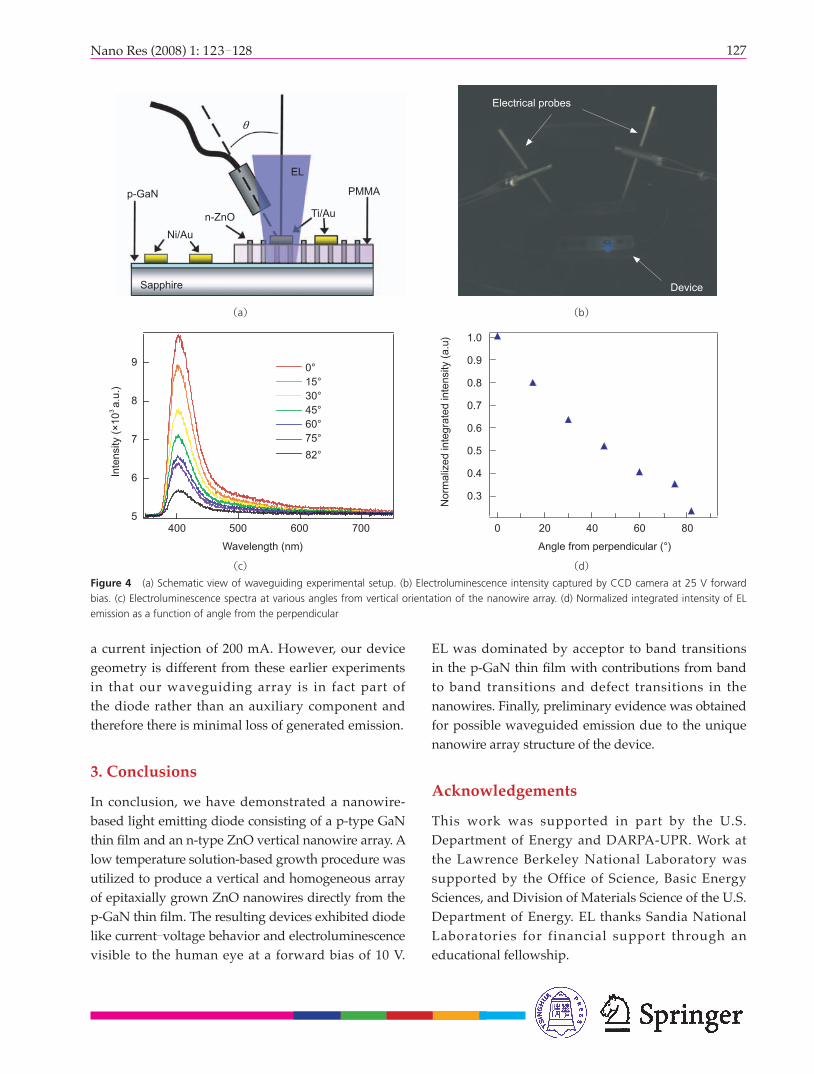
One of the advantages of using a vertical nanowire array over a thin fi lm is the potential for waveguided emission, and therefore the potential for improved extraction efficiency. The natural unseeded epitaxial growth of the ZnO nanowires from the p-GaN thin fi lm yielded fairly large diameters around 100 600 nm.An ideal single mode waveguide cavity would be around 200 nm for a ZnO material surrounded by a medium of PMMA in this wavelength regime [23]. For the waveguiding experimental setup, a modifi ed EL setup was used. The collecting optical fiber was placed directly above the luminescence site at angles ranging from 0˚ to 90˚ from the normal (Fig. 4(a)). At every measurement, the radial position of the end of the optical fiber was exactly 1 cm from the surface of the device. Figure 4(c) shows electroluminescence spectra at various angles from the normal and Fig. 4(d) shows the correlation between normalized integrated EL intensity for the various positions.
The strongest emission intensity was observed at 0˚ from normal (directly on top of the device), and the intensity rapidly decays as detection angle increases. This observation suggests that part of the junction emission might be directly waveguided to the tip of the nanowires. A similar setup has been investigated previously, employing a vertical ZnO nanorod array as a waveguiding mechanism for emission from a traditional GaN-based multiple quantum well (MQW) thin film LED [24, 25]. Increases of 50% and 100% in light output at applied currents of 20 and 50 mA, respectively, were reported by An et al. [24] whilst Chiu et al. reported a 38.4% light output increase for
Figure 3 Solution-grown-ZnO nanowire LED device: (a) schematic view of device and location of electroluminescence; (b) I V curves; (c) photoluminescence spectra; (d) electroluminescence spectra
p-GaN
Ni/Au
n-ZnO
EL
Ti/Au
PMMA
Sapphire
200
150
100
50
0–8 –6 –4 –2 0 2 4 6 8
Voltage (V)
Cur
rent
(μ
A)
140
120
100
80
60
40
20
Inte
nsity
(×
103 a.
u.)
Wavelength (nm)
300 400 500 600 700 800
n-ZnO nanowire arrayp-GaN thin fi lm
22
20
18
16
14
12
10
8
6
Inte
nsity
(×
103 a.
u.)
300 400 500 600 700 800
Bias voltage (V)0 5 10 15 20 25
Wavelength (nm)
(a)
(b)
(c)
(d)
127Nano Res (2008) 1: 123 128
a current injection of 200 mA. However, our device geometry is different from these earlier experiments in that our waveguiding array is in fact part of the diode rather than an auxiliary component and therefore there is minimal loss of generated emission.
3. Conclusions
In conclusion, we have demonstrated a nanowire-based light emitting diode consisting of a p-type GaN thin fi lm and an n-type ZnO vertical nanowire array. A low temperature solution-based growth procedure was utilized to produce a vertical and homogeneous array of epitaxially grown ZnO nanowires directly from the p-GaN thin fi lm. The resulting devices exhibited diode like current voltage behavior and electroluminescence visible to the human eye at a forward bias of 10 V.
p-GaN
Ni/Au
n-ZnO
EL
Ti/Au
PMMA
Sapphire
θ
9
8
7
6
5400 500 600 700
0°15°30°45°60°75°
82°
Wavelength (nm)
Inte
nsity
(×
103 a.
u.)
1.0
0.9
0.8
0.7
0.6
0.5
0.4
0.3
0 20 40 60 80
Angle from perpendicular (°)
Nor
mal
ized
inte
grat
ed in
tens
ity (
a.u)
(a) (b)
(c) (d)Figure 4 (a) Schematic view of waveguiding experimental setup. (b) Electroluminescence intensity captured by CCD camera at 25 V forward bias. (c) Electroluminescence spectra at various angles from vertical orientation of the nanowire array. (d) Normalized integrated intensity of EL emission as a function of angle from the perpendicular
Electrical probes
Device
EL was dominated by acceptor to band transitions in the p-GaN thin fi lm with contributions from band to band transitions and defect transitions in the nanowires. Finally, preliminary evidence was obtained for possible waveguided emission due to the unique nanowire array structure of the device.
Acknowledgements
This work was supported in part by the U.S. Department of Energy and DARPA-UPR. Work at the Lawrence Berkeley National Laboratory was supported by the Office of Science, Basic Energy Sciences, and Division of Materials Science of the U.S. Department of Energy. EL thanks Sandia National Laboratories for financial support through an educational fellowship.

128 Nano Res (2008) 1: 123 128
Nano Research
References
[1] Strite, S.; Morkoç, H. GaN, AlN, and InN: A review. J. Vac.
Sci. Technol. B 1992, 10, 1237 1266.
[2] Wang, Z. L. Zinc oxide nanostructures: Growth, properties
and applications. J. Phys.: Condens. Mat. 2004, 16, R829
R858.
[3] Sirbuly, D. J.; Law, M.; Yan, J.; Yang, P. Semiconductor
nanowires for subwavelength photonics integration. J.
Phys. Chem. B 2005, 109, 15190 15213.
[4] Duan, X.; Huang, Y.; Cui, Y.; Wang, J.; Lieber, C. M.
Indium phosphide nanowires as building blocks for
nanoscale electronic and optoelectronic devices. Nature
2001, 409, 66 69.
[5] Khan, A.; Balakrishnan, K.; Katona, T. Ultraviolet light-
emitting diodes based on group three nitrides. Nat.
Photon. 2008, 2, 77 84.
[6] Pearton, S. J.; Ren, F.; Zhang, A. P.; Lee, K. P. Fabrication
and performance of GaN electronic devices. Mater. Sci.
Eng. R 2000, 30, 55 212.
[7] Greene, L. E.; Law, M.; Goldberger, J.; Kim, F.; Johnson,
J. C.; Zhang, Y.; Saykally, R. J.; Yang, P. Low-temperature
nanowire arrays. Angew. Chem. Int. Ed. 2003, 42, 3031
3034.
[8] Ohgaki, T.; Sugimura, S.; Ryoken, H.; Ohashi, N.;
Sakaguchi, I.; Sekiguchi, T.; Haneda, H. Interfacial structure
of GaN and InN thin fi lms grown on ZnO substrates. Key
Eng. Mat. 2006, 301, 79 82.
[9] Johnson, J.; Yan, H.; Schaller, R. D.; Haber, L. H.; Saykally,
R. J.; Yang, P. Single nanowire lasers. J. Phys. Chem. B
2001, 105, 11387 11390.
[10] Law, M.; Sirbuly, D. J.; Johnson, J. C.; Goldberger, J.;
Saykally, R. J.; Yang, P. Nanoribbon waveguides for
subwavelength photonics integration. Science 2004,
305, 1269 1272.
[11] Park, W. I.; Yi, G. C. Electroluminescence in n-ZnO
nanorod arrays vertically grown on p-GaN. Adv. Mater.
2004, 16, 87 90.
[12] Kim, D. C.; Han, W. S.; Kong, B. H.; Cho, H. K.; Hong, C.
H. Fabrication of the hybrid ZnO LED structure grown on
p-type GaN by metal organic chemical vapor deposition.
Physica B 2007, 401 402, 386 390.
[13] Jeong, M. C.; Oh, B. Y.; Ham, M. H.; Lee, S. W.; Myoung,
H. M. ZnO-nanowire-inserted GaN/ZnO heterojunction
light-emitting diodes. Small 2007, 3, 568 572.
[14] Sun, H.; Zhang, Q. F.; Wu, J. L. Electroluminescence
from ZnO nanorods with an n-ZnO/p-Si heterojunction
structure. Nanotechnology 2006, 17, 2271 2274.
[15] Könenkamp, R.; Word, R. C.; Godinez, M. Ultraviolet
electroluminescence from ZnO/polymer heterojunction
light-emitting diodes. Nano Lett. 2005, 5, 2005 2008.
[16] Chang, C. Y.; Tsao, F. C.; Pan, C. J.; Chi, G. C.; Wang, H. T.;
Chen, J. J.; Ren, F.; Norton, D. P.; Pearton, S. J.; Chen, K.
H.; Chen, L. C. Electroluminescence from ZnO nanowire/
polymer composite p n junction. Appl. Phys. Lett. 2006,
88, 173503.
[17] Nadarajah, A.; Word, R. C.; Meiss, J.; Könenkamp, R.
Flexible inorganic nanowire light-emitting diode. Nano
Lett. 2008, 8, 534 537.
[18] Yang, W. Q.; Huo, H. B.; Dai, L.; Ma, R. M.; Liu, S. F.; Ran,
G. Z.; Shen, B.; Lin, C. L.; Qin, G. G. Electrical transport
and electroluminescence properties of n-ZnO single
nanowires. Nanotechnology 2006, 17, 4868 4872.
[19] Lee, S. K.; Kim, T. H.; Lee, S. Y.; Choi, K. C.; Yang, P.
High-brightness gallium nitride nanowire UV-blue light
emitting diodes. Philos. Mag. 2007, 87, 2105 2115.
[20] Motayed, A.; Davydov, A. V.; He, M.; Mohammad, S. N.;
Melngailis, J. 365 nm operation of n-nanowire/p-gallium
nitride homojunction light emitting diodes. Appl. Phys.
Lett. 2007, 90, 183120.
[21] Zimmler, M. A.; Bao, J.; Shalish, I.; Yi, W.; Yoon, J.;
Narayanamurti, V.; Capasso, F. Electroluminescence from
single nanowires by tunnel injection: An experimental
study. Nanotechnology 2007, 18, 1 5.
[22] Viswanath, A. K.; Shin, E. J.; Lee, J. I.; Yu, S.; Kim, D.;
Kim, B.; Choi, Y.; Hong, C. H. Magnesium acceptor levels
in GaN studies by photoluminescence. J. Appl. Phys.
1998, 83, 2272 2275.
[23] Johnson, J. C.; Yan, H.; Yang, P.; Saykally, R. J. Optical
cavity effects in ZnO nanowire lasers and waveguides. J.
Phys. Chem. B 2003, 107, 8816 8828.
[24] An, S. J.; Chae, J. H.; Yi, G. C.; Park, G. H. Enhanced
light output of GaN-based light-emitting diodes with
ZnO nanorod arrays. Appl. Phys. Lett. 2008, 92, 121108.
[25] Chiu, C. H.; Lee, C. E.; Chao, C. L.; Cheng, B. S.; Huang,
H. W.; Kuo, H. C.; Lu, T. C.; Wang, S. C.; Kuo, W. L.
Hsiao, C. S.; Chen, S. Y. Enhancement of light output
intensity by integrating ZnO nanorod arrays on GaN-
based LLO vertical LEDs. Electrochem. Solid-State Lett.
2008, 11, H84 H87.