Verilog Hardware Description Language -...
42
Transcript of Verilog Hardware Description Language -...
Content
Lecture 1: Computer organization and performance evaluation metrics
Lecture 2: Processor architecture and memory system
Lecture 3: Logic circuit: Combinational circuit and sequential circuit
Lecture 4: Number system and Its Importance
Lecture 5: Hardware design by HDL
Lecture 6: Parallel programming
Lecture 7: Hardware design by high-level synthesis
Lecture 8: Computer system design and its applications
2

Lecture Information
3

Grading (評価)Mini-test (40%) Score is based on the number of times that you attend the class and your
enthusiastic on doing mini-test.
You may get MAX score although your answer is not correct!
If you cannot attend the lecture with reasonable reason (ex: attend conference), you can get MAX score if you: Inform about your absent to me via email: [email protected]
Study from lecture video and submit mini-test by next time.
Home-work: (60%) Score is based on the correction of your home-work
Bonus (+10%) Your activeness, enthusiastic during the lecture (make question, answer the question,
etc.)
4
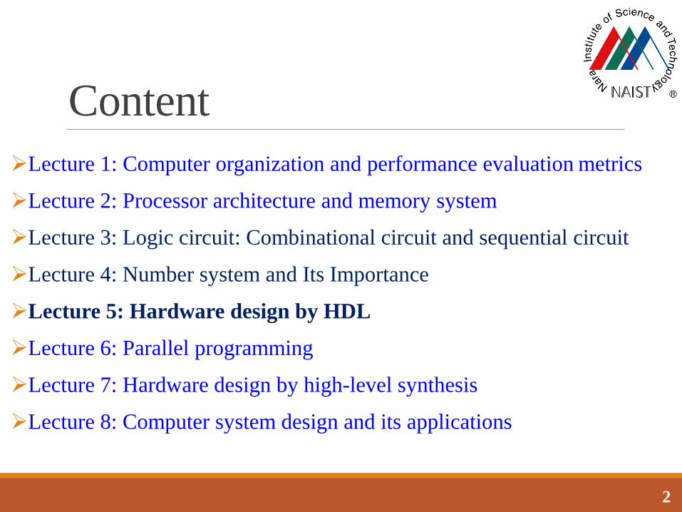
Overview of Hardware Circuit Design
Block
1
Binary Logic gate:
Not, And, Or, etc.
Transistors
System Block
2
Block
N…
Comb. Circuit: Do specific
function.
Seq. Circuit: Register,
memory, etc.
Adder Mul.
MUX Comp.
Latch Flipflop
Comparator
Adder Register Memory
Hardware System
Analog
Circuit
Design
Digital
Circuit
Design
Verilog HDL
5

Contents
Verilog HDL
Sample Designs
Quartus II
6

Hardware Description Languages (HDL)
Describe the hardware circuit by using codes Code is synthesized into logic gates
Require libraries of standard cells
Widely used in logic design
Verilog HDL and VHDL (Very High Speed Integrated Circuit HDL)
Verilog /
VHDL
Example of netlist
netlist
CompilerStandard cell
LibrariesQuartus II
7

Verilog
Verilog is one of the two major HDL used in industry and academia
Verilog is easier than VHDL
Digital systems are highly complex Verilog makes the digital circuit design becomes simple.
4-bit adder
8

ModuleBasic Unit of Verilog is: MODULE
◦ Describes the functionality of the design
◦ States the input and output ports
module module_name ( port_list );
port declarations;
…
variable declaration;
…
description of behavior
endmodule
General Definition Example
module adder_4bit
9

Numbers
Numbers are specified in the form:
<size><base format><Value>
Size: Number of bits that represents the number
Base format: b (binary); d (decimal); o (octal); h (hex)
Value: value of the number
Examples:◦ 4’b0110: 4-bit binary number with value 0110
◦ 8’hf7 : 8-bit hexadecimal number with value f7
◦ 16’d80: 16-bit decimal number with value 80
10

Quiz
What is the meaning of the following numbers?
6’b011000
8’d20
16’h093f
32’d100
9’o725
11

Signal Declaration Internal signals:
◦ Net: wire <size> <name> ;
◦ Register: reg <size> <name> ;
Example:
Port signals:
Input port: input <size> <name> ;
Output port:
◦ Net: output <size> <name> ;
◦ Register: output reg <size> <name> ;
When should a signal be
declared as a net / a
register ?
12

“assign” versus “always” (1/2)Assignment :
◦ Format: assign <LHS> = <RHS>;
◦ Means that whenever any change on the RHS occurs, it will be evaluated and assigned to the LHS.
◦ LHS must be a net type signal.
◦ Example:
13

Always blocks
◦ Describe events that should happen under certain conditions.
◦ The LHS of commands inside “always” block must be Register type
◦ Two kinds of “Always” blocks
always @(posedge clock) begin
LHS-1 <= RHS-1
end
always @(<signal list>) begin
LHS-2 = RHS-2
end
Type-1: describes the sequential
logic (or register). The LHS will
change its value at the positive or
negative edge of clock signal
Type-2: describes the
combinational block (or logic
gate). The LHS will change its
value when one or more signals in
the list change the value
“assign” versus “always” (2/2)
14
What kind of memory that LHS-1 and LHS-2 should be ?

“assign” versus “always” Example (1/3)
always
assign
15

always
assign
“assign” versus “always” Example (2/3)
16

always
assign
“assign” versus “always” Example (3/3)
17
What is the different between two waveforms ?

CommentsComment:
◦ “//” : one line comment
◦ “/* */ “ : multi-lines comment
Note: The language is case sensitive
example: “a” and “A” are different
18

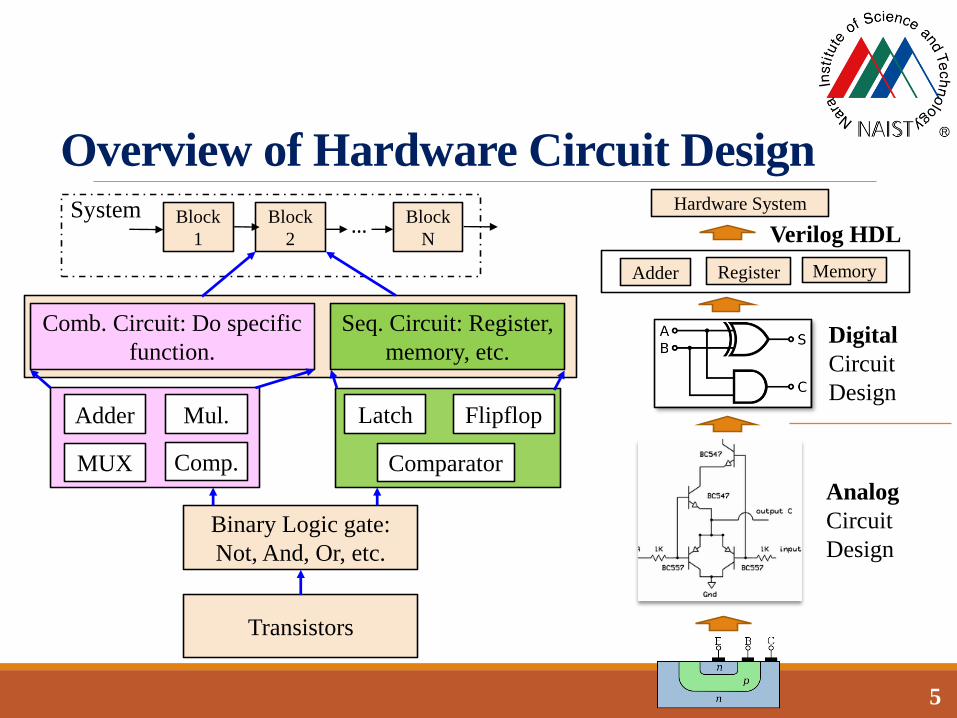
If … else… versus case commands
always @(…) begin
if ( <condition> ) begin
...
end
else if ( <condition> ) begin
...
end
else begin
...
end
end
if (datain == 2’b00) begindatao <= 2;
endelse if (datain == 2’b01) begin
datao <= 5;endelse begin
datao <= 10;end
Example:
These commands can be used inside always blocks only.
19
If … else… versus case commands
always @(…) begin
case (<signal name>)
<value 1> : command 1;
<value 2> : command 2;
…
default: command n;
endcase
end
case (datain)2’b00: datao <= 2;2’b01: datao <= 5;
default: datao <= 10;endcase
Example:
These commands can be used inside always blocks only.
20

Verilog Basic Commands (1/6)
assign c = (a < b);
If: a=3, b=4 c = 1
a = 5, b = 2 c = 0
21
22
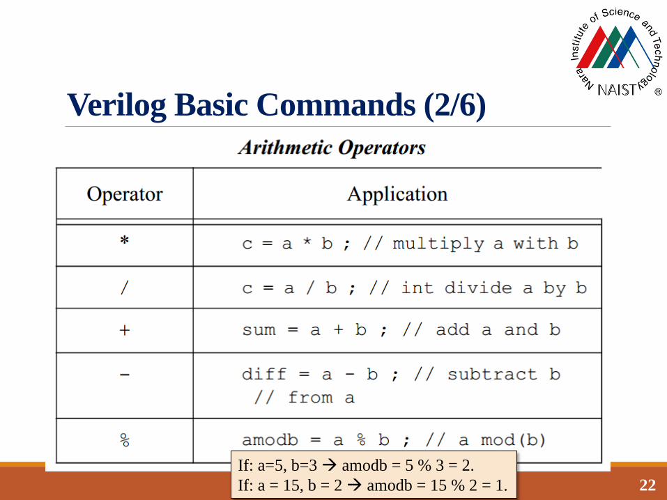
Verilog Basic Commands (2/6)
If: a=5, b=3 amodb = 5 % 3 = 2.
If: a = 15, b = 2 amodb = 15 % 2 = 1.

Mainly
used to
present
condition
inside if
command
23
Verilog Basic Commands (3/6)

Mainly
used to
present
condition
of if
command
assign
command
24
Verilog Basic Commands (4/6)
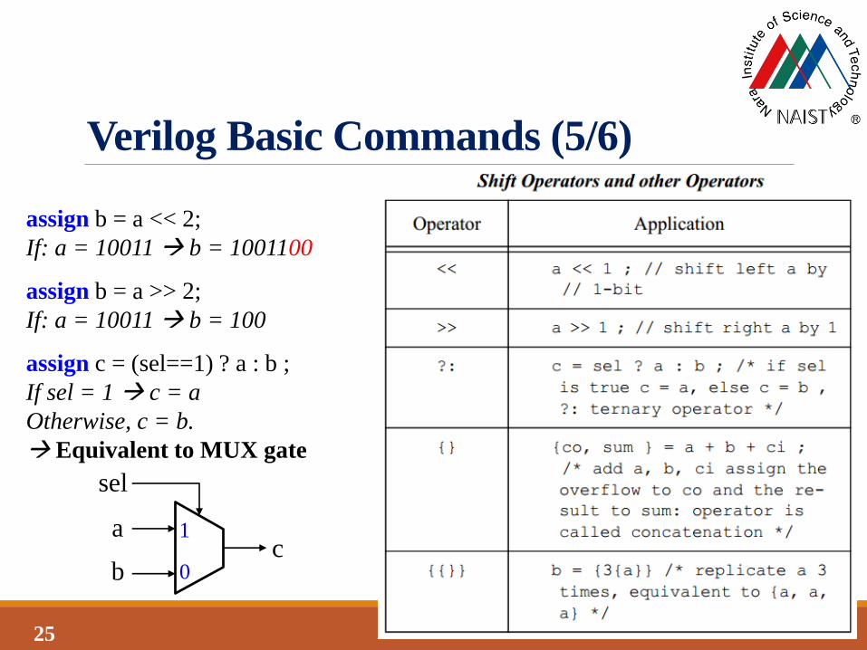
assign b = a << 2;
If: a = 10011 b = 1001100
assign b = a >> 2;
If: a = 10011 b = 100
assign c = (sel==1) ? a : b ;
If sel = 1 c = a
Otherwise, c = b.
Equivalent to MUX gate
25
Verilog Basic Commands (5/6)
a
bc
sel
1
0
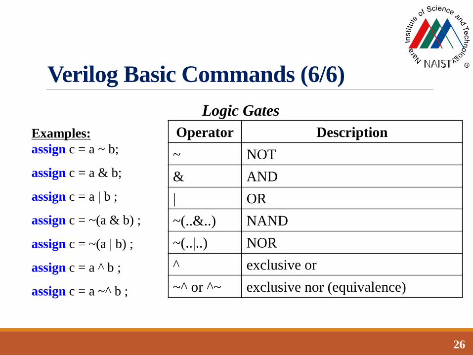
Operator Description
~ NOT
& AND
| OR
~(..&..) NAND
~(..|..) NOR
^ exclusive or
~^ or ^~ exclusive nor (equivalence)
26
Verilog Basic Commands (6/6)
Logic Gates
Examples:
assign c = a ~ b;
assign c = a & b;
assign c = a | b ;
assign c = ~(a & b) ;
assign c = ~(a | b) ;
assign c = a ^ b ;
assign c = a ~^ b ;

Sample design 1
Wire_1
Wire_2
Y
28
Write Verilog code for below circuits:
The Generated netlist:

Sample design 2
Wire_1
Wire_2
Y
29
Write Verilog code for below circuits:
clk

30
Verilog codeGenerated netlist
Sample design 2 - Answer
31
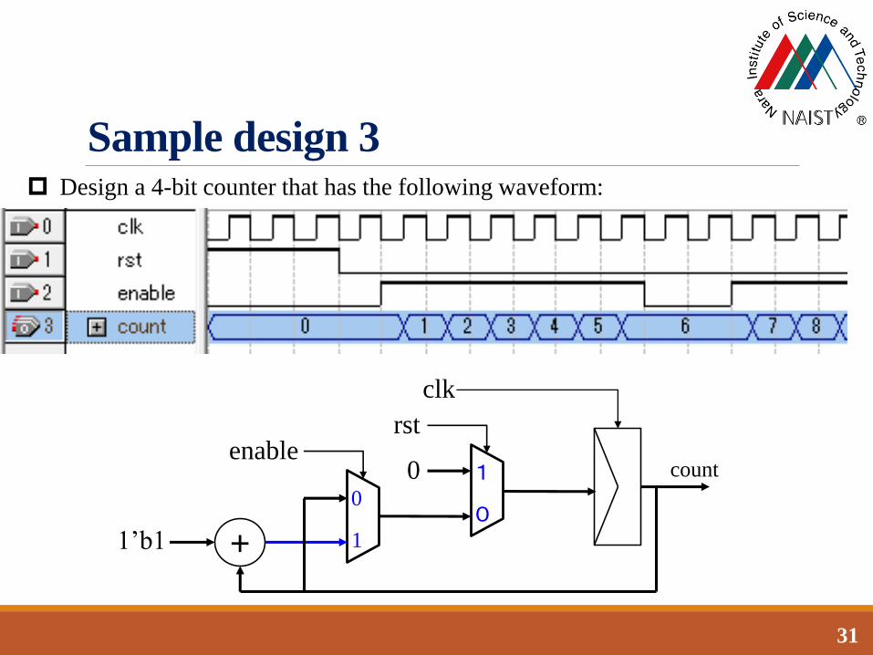
Design a 4-bit counter that has the following waveform:
count
+
0
rst
1
0
enable
0
11’b1
clk
Sample design 3

32
Sample design 3 - Answer

33
Sample design 4
Sample_4
clk
rst
enable
count
1
1
1
3
Design a counter that has the following waveform:
How many bits are needed for count signal?
34
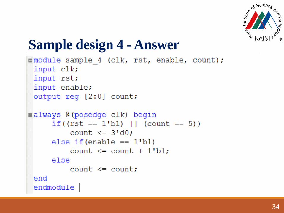
Sample design 4 - Answer
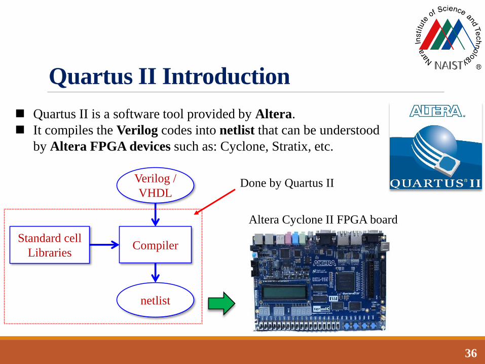
Quartus II Introduction
36
Quartus II is a software tool provided by Altera.
It compiles the Verilog codes into netlist that can be understood
by Altera FPGA devices such as: Cyclone, Stratix, etc.
Verilog /
VHDL
netlist
CompilerStandard cell
Libraries
Altera Cyclone II FPGA board
Done by Quartus II
Summary
Lecture 3: Logic circuit: Combinational circuit and sequential circuit
Lecture 4: Number system and Its Importance
Lecture 5: Hardware design by HDL
37
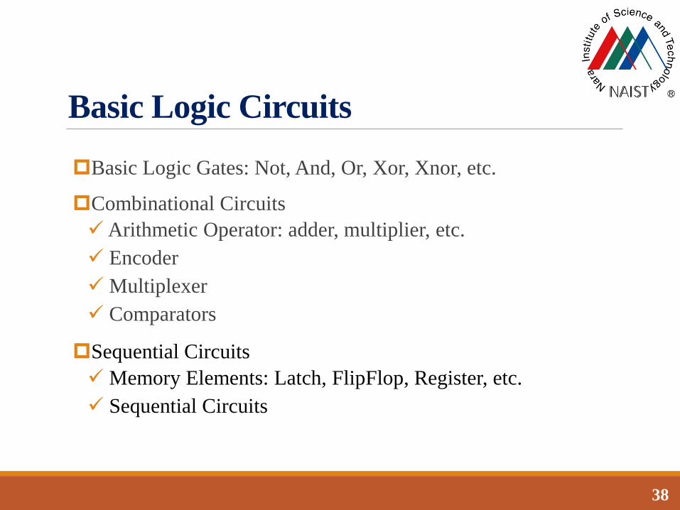
Basic Logic Circuits
Basic Logic Gates: Not, And, Or, Xor, Xnor, etc.
Combinational Circuits
Arithmetic Operator: adder, multiplier, etc.
Encoder
Multiplexer
Comparators
Sequential Circuits
Memory Elements: Latch, FlipFlop, Register, etc.
Sequential Circuits
38

Number Systems
Number System Introduction Number systems used by humanNumber systems used by computer: binary, decimal, octal, hexa-decimal
Number System Conversion
Signed Number RepresentationSign-magnitudeOne’s complementTwo’s complement
Fractional Number RepresentationFixed point numberFloating point number
Size of Number: Complexity vs. Performance
39

Verilog HDL
Verilog HDLModule
Always v.s. Assign
If … else… command
Case command
Verilog Basic commands
Sample Designs
Quartus II
40

Next Class
先進情報科学特別講義Ⅱ,Ⅳ(130047, 130049)
Advanced Cutting-edge
Research Seminar Ⅱ&Ⅳ(130047, 130049)
41
Time: 12月1, 6, 8, 13日 9:20--10:50
Course Name:
Research Trends on High Throughput Wireless Communication Systems
(高スループット無線通信システムに関する研究動向)
Place: L1 room
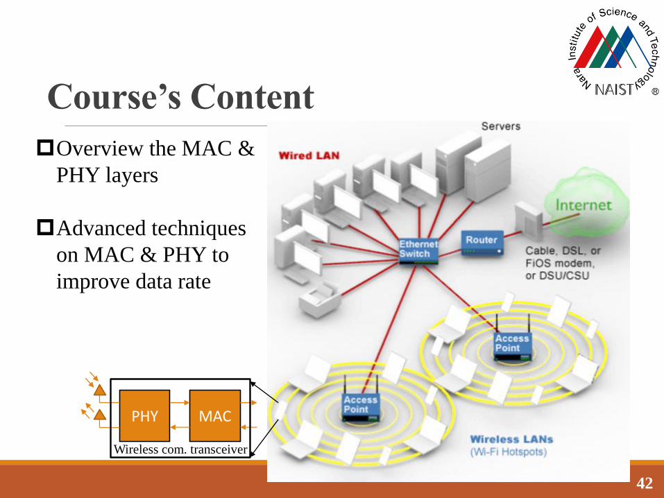
Course’s Content
42
PHY MAC
Wireless com. transceiver
Overview the MAC &
PHY layers
Advanced techniques
on MAC & PHY to
improve data rate