Vedic Architecture for Math Processors€¦ · The Booth recording multiplier is one such...
54
PIIT Journal of Electronics Engineering 1 Vedic Architecture for Math Processors Jayesh R. Koli, Aniket Mhatre, Deepak Kumar, Vibhu Layal Department of Department of Department of Department of Electronics Engineering, Electronics Engineering, Electronics Engineering Electronics Engineering PIIT PIIT PIIT PIIT New Panvel, New Panvel New Panvel New Panvel Maharashtra, India Maharashtra, India Maharashtra, India Maharashtra India [email protected] [email protected] [email protected] [email protected] Abstract - A typical processor consists of ALU (Arithmetic and Logic Unit) which performs all the arithmetic operations which is assigned to it, hence the computing power of the processor is totally based on it. Nowadays we are obsessed with the high end fast processors to be in are cell phones, laptops, desktops etc. So there has been race among the designers to design very high speed, and compact processor for the upcoming electronic devices. Even though the designers have succeeded in designing very high speed processors but most of them lack due to space complexity and power consumption. Thus this paper gives an ancient Indian technique known as Vedic Mathematics which is utilized to implement multiplier and divider for fast multiplication and division etc. It will give best results in terms of speed, area and power consumption. Keywords: space complexity, latency, Vedic Mathematics, multiplier, divider. I. INTRODUCTION For any DSP processor which controls LCD has to do multiplication and division for n number of times that also in very short time in the range of nanoseconds. So there have been many algorithms devised for multiplication and division in DSP‘s some of them are Wallace tree, Array multiplier, Booth‘s algorithm etc. Out of them Booth‘s algorithm is the fastest algorithm for multiplication but it has two disadvantages one is complex circuitry another is more power consumption. II. OBJECTIVE The objective of the good multiplier and divider is to provide a compact, high speed and low power consumption unit. Being an essential part of arithmetic processing unit multipliers and dividers are in extremely high demand on its speed and low power consumption. To reduce the significant power consumption the design should involve less number of operations so as to diminish the dynamic power consumption which is dominant of all. Also the design could be easily implemented using VLSI technology. III. VARIOUS METHODS AND ITS PROS AND CONS There are many ways to perform multiplication in binary system. It depends on the performance factors like latency, throughput, area, and design complexity. Some of them are explained below. A. Array Multiplier
Transcript of Vedic Architecture for Math Processors€¦ · The Booth recording multiplier is one such...

PIIT Journal of Electronics Engineering 1
Vedic Architecture for Math Processors
Jayesh R. Koli, Aniket Mhatre, Deepak Kumar, Vibhu Layal
Department of Department of Department of Department of
Electronics Engineering, Electronics Engineering, Electronics Engineering Electronics Engineering
PIIT PIIT PIIT PIIT
New Panvel, New Panvel New Panvel New Panvel
Maharashtra, India Maharashtra, India Maharashtra, India Maharashtra India
[email protected] [email protected] [email protected] [email protected]
Abstract - A typical processor consists of ALU
(Arithmetic and Logic Unit) which performs all the
arithmetic operations which is assigned to it, hence the
computing power of the processor is totally based on it.
Nowadays we are obsessed with the high end fast processors
to be in are cell phones, laptops, desktops etc. So there has
been race among the designers to design very high speed,
and compact processor for the upcoming electronic
devices. Even though the designers have succeeded in
designing very high speed processors but most of them lack
due to space complexity and power consumption. Thus this
paper gives an ancient Indian technique known as Vedic
Mathematics which is utilized to implement multiplier and
divider for fast multiplication and division etc. It will give
best results in terms of speed, area and power consumption.
Keywords: space complexity, latency, Vedic Mathematics,
multiplier, divider.
I. INTRODUCTION
For any DSP processor which controls LCD has to do
multiplication and division for n number of times that also in
very short time in the range of nanoseconds. So there have been
many algorithms devised for multiplication and division in
DSP‘s some of them are Wallace tree, Array multiplier, Booth‘s
algorithm etc. Out of them Booth‘s algorithm is the fastest
algorithm for multiplication but it has two disadvantages one
is complex circuitry another is more power consumption.
II. OBJECTIVE
The objective of the good multiplier and divider is
to provide a compact, high speed and low power consumption
unit. Being an essential part of arithmetic processing unit
multipliers and dividers are in extremely high demand on its
speed and low power consumption. To reduce the significant
power consumption the design should involve less number of
operations so as to diminish the dynamic power consumption
which is dominant of all. Also the design could be easily
implemented using VLSI technology.
III. VARIOUS METHODS AND ITS PROS AND CONS
There are many ways to perform multiplication in binary
system. It depends on the performance factors like latency,
throughput, area, and design complexity. Some of them are
explained below.
A. Array Multiplier

PIIT Journal of Electronics Engineering 2
Array multiplier is an efficient layout of a combinational
multiplier which performs the 1x1 bit multiplication.
The array multiplier is as shown below.
Figure1. Array multiplier
Array Multiplier gives more power consumption as well
as optimum number of components required, but delay for this
multiplier is larger. It also requires larger number of gates
because of which area is also increased; due to this array
multiplier is less economical. Thus, it is a fast multiplier but
hardware complexity is high.
B. Wallace tree multiplier
A fast process for multiplication of two numbers was
developed by Wallace. Using this method, a three step process is
used to multiply two numbers; the bit products are formed, the
bit product matrix is reduced to a two row matrix where sum
of the row equals the sum of bit products, and the two resulting
rows are summed with a fast adder to produce a final
product.Wallace tree is a tree of carry-save adders arranged
products are formed, the bit product matrix is reduced to a two
row matrix where sum of the row equals the sum of bit products,
and the two resulting rows are summed with a fast adder to
produce a final product.Wallace tree is a tree of carry-save
adders arranged as shown in figure 2
Figure2. Wallace tree multiplier
A carry save adder consists of full adders like the more familiar
ripple adders, but the carry output from each bit is brought out
to form second result vector rather being thanwired to the
next most significant bit. The carry vector is 'saved' to be
combined with the sum later. In the Wallace tree method, the
circuit layout is not easy although the speed of the operation is
high since the circuit is quite irregular.
C. Booth multiplier
Another improvement in the multiplier is by reducing
the number of partial products generated.
The Booth recording multiplier is one such multiplier; it scans
the three bits at a time to reduce the number of partial products.
These three bits are: the two bit from the present pair; and a third
bit from the high order bit of an adjacent lower order pair. After
examining each triplet of bits, the triplets are converted by
Booth logic into a set of five control signals used by the
adder cells in the array to control the operations performed by
the adder cells.
To speed up the multiplication Booth encoding performs several
steps of multiplication at once. Booth‘s algorithm takes
advantage of the fact that an adder subtractor is nearly as fast
and small as a simple adder.
The method of Booth recording reduces the
numbers of adders and hence the delay required to produce the

PIIT Journal of Electronics Engineering 3
partial sums by examining three bits at a time. The high
performance of booth multiplier comes with the drawback of
power consumption. The reason is large number of adder cells
required that consumes large power.
IV.ANCIENT INDIAN VEDIC METHOD FOR
MULTIPLICATION
The idea for designing the multiplier and adder unit was adopted
from ancient Indian mathematics ―Vedas‖. Based on those
formulae, the partial products and sums are generated in single
step which reduces the carry propagation from LSB to MSB.
The implementation of the Vedic mathematics and their
application to the complex multiplier ensured substantial
reduction of propagation delay in comparison with Distributed
Array (DA) based architecture and parallel adder based
implementation which are most commonly used architectures.
Reduced bit multiplication algorithm for digital
arithmetic is shown. It mainly consisted of the in depth
explanation of Urdhva tiryakbhyam sutra and the Nikhilam
sutra. These sutras are the extracts from the Vedas which are the
store house of knowledge. The former is suggested for smaller
numbers and the latter is suggested for larger numbers.
A. Urdhva-Tiryagbhyam Sutra
Urdhva-tiryagbhyam sutra is the general formula
applicable to all cases of multiplication and also very useful in
the division of a large number by another large number.
The formula itself is very short and terse, consisting of
only one compound word and means ―vertically and cross-wise‖.
It results in the generation of all partial products along with the
concurrent addition of these partial products in parallel. Since
there is a parallel generation of the partial products and their
sums, the processor becomes independent of the clock
frequency. The advantage here is that parallelism reduces the
need of processors to operate at increasingly high clock
frequencies. A higher clock frequency will result in increased
processing power, and its demerit is that it will lead to
increased power dissipation resulting in higher device
operating temperatures.
By employing the Vedic multiplier, all the demerits
associated with the increase in power dissipation can be
negotiated. Since it is quite faster and efficient its layout has a
quite regular structure. Owing to its regular structure, its layout
can be done easily on a silicon chip. The Vedic multiplier
has the advantage that as the number of bits increases, gate delay
and area increases very slowly as compared to other multipliers,
thereby making it time, space and power efficient. It is
demonstrated that this architecture is quite efficient in terms of
silicon area/speed.
The illustration of this method is considered with the
multiplication of two decimal numbers 123 and 135
By western method
123
X 135
615
3690
12300
16605
By urdhva-tiryakbhyam sutra:
1. We multiply the left-hand-most digits vertically to obtain
the left-hand-most part of the answer; 1x1=1
2. Then we multiply 1 and 3, and 1 and 2 cross-wise and add
the result to get the sum 5 as the second part of the answer.
3.Then we multiply cross-wise1 and 5, and 1 and 3 and,
vertically 2 and 3 and add the result to get the sum 14 as the
third part of the answer.
4.Then multiply 2 and 5, and 3 and 3 crosswise and add the

PIIT Journal of Electronics Engineering 4
result to get the sum 14 as the fourth part of the answer.
5.Then multiply right-hand-most digits 3 and 5 to get the result
15 as the last part of the answer. The partial products so
obtained is written as shown below
123
135
1:5:14:19:15
998
X 997
6986
89820
898200
995006
We can write the final answer as
123
135
1:5:4:9:5
0:1:1:1:0
1 6 6 0 5
This method is very useful when the numbers are small
to moderate but what happens if the numbers are very large, for
that purpose the Vedic math has given another technique which
is efficient for multiplication of large numbers it is Nikhilam
Sutra.
B. Nikhilam Sutra
The sutra reads Nikhilam Navatascaramam Dasatah
which, literally translated, means: ―all from 9 and last from
10‖.Suppose we have to multiply two large numbers 998 and
997.
By western method:
998
X 997
6986
89820
898200
995006
By nikhilam sutra:
1. We first select our base for the calculation which is the power
of 10 and nearest to the numbers to be multiplied.
2. In this case the base is 1000 and we calculate the deficiency
of each number from 1000.
3. For 998 it is 002 while for 997 it is 003
4. Then we append negative sign as the numbers are less
than 1000.
998 -002
997 -003
5. Now we can write the right-most-part of the answer by
multiplication of the deficits which is -002x-003=006.
6. To obtain the left-most-part of the answer we subtract 003
from 998 or subtract 002 from 997 to get the result as 995.
7. Thus we can write the final answer as shown below.
998 -002
997 -003
995 /006
Hence we conclude that urdhva tiryakbhyam gives best
result for the small numbers while nikhilam sutra is good at
large numbers. So by integrating these two modules, we can
design an efficient and intelligent multiplier.
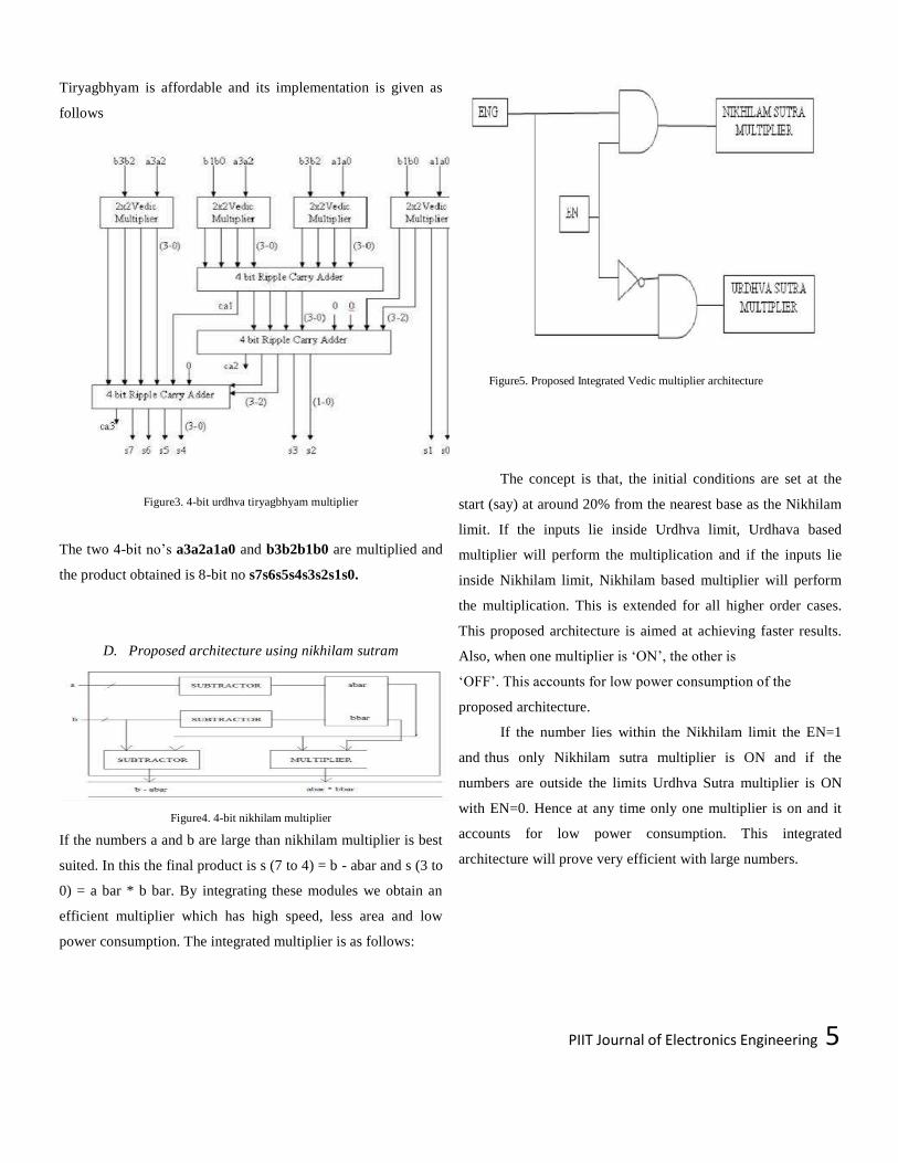
C. Proposed architecture using urdhva tiryagbhyam
If the numbers are small then multiplication with Urdhva
PIIT Journal of Electronics Engineering 5
Tiryagbhyam is affordable and its implementation is given as
follows
Figure3. 4-bit urdhva tiryagbhyam multiplier
The two 4-bit no‘s a3a2a1a0 and b3b2b1b0 are multiplied and
the product obtained is 8-bit no s7s6s5s4s3s2s1s0.
D. Proposed architecture using nikhilam sutram
Figure4. 4-bit nikhilam multiplier
If the numbers a and b are large than nikhilam multiplier is best
suited. In this the final product is s (7 to 4) = b - abar and s (3 to
0) = a bar * b bar. By integrating these modules we obtain an
efficient multiplier which has high speed, less area and low
power consumption. The integrated multiplier is as follows:
Figure5. Proposed Integrated Vedic multiplier architecture
The concept is that, the initial conditions are set at the
start (say) at around 20% from the nearest base as the Nikhilam
limit. If the inputs lie inside Urdhva limit, Urdhava based
multiplier will perform the multiplication and if the inputs lie
inside Nikhilam limit, Nikhilam based multiplier will perform
the multiplication. This is extended for all higher order cases.
This proposed architecture is aimed at achieving faster results.
Also, when one multiplier is ‗ON‘, the other is
‗OFF‘. This accounts for low power consumption of the
proposed architecture.
If the number lies within the Nikhilam limit the EN=1
and thus only Nikhilam sutra multiplier is ON and if the
numbers are outside the limits Urdhva Sutra multiplier is ON
with EN=0. Hence at any time only one multiplier is on and it
accounts for low power consumption. This integrated
architecture will prove very efficient with large numbers.

PIIT Journal of Electronics Engineering 6
V. ANCIENT INDIAN VEDIC METHOD FOR DIVISION
There are number of Vedic division methods like
Nikhilam Sutram, Paravartya Sutram, and Dhvajank Sutram etc.
A. Paravartya Sutra
We first describe here the Paravartya sutra which is
special case formula and read as ―Paravartya Yojayet‖ and
which means ―Transpose and apply‖.
Suppose we have to divide 1234 by 112
Figure6. division using Paravartya Sutra
1. The divisor 112 is written on the left then we transpose
all the digits except the leftmost digit write it down below as
-1 -2, this is modified 10‘s complement.
2. Put as many digits of the dividend on the right as there are
digits in the modified 10‘s complement. It gives the remainder
digits while right digits give the quotient.
3. Then directly write down the first digit as it is.
4. Then multiplying 1 by the 10‘s complement, we get 1 x -1 -
2 = -1 -3. Put -1 below the second digit and -
3 below the third digit of the dividend.
5. Now add the numbers under the second digit of the
dividend it get 2 + -1 = 1. Then put this sum directly below it.
Now multiply 1 with the modified 10‘ complement to get 1 x -
1 -2 = -1 -2.
6. Put -1 below the third and -2 below the fourth digit of the
dividend. Now add up the numbers under the third digit to get 3
+ -2 + -1 = 0. Put it at the bottom. Now add up the numbers
under the fourth digit to get 4 + -2 = 2. Put it at the bottom.
7. Thus we get the 11 as quotient and 02 as remainder.
73) 1 11
27 27
1 38
1. Here divisor is 73 and dividend is 111. So we find the 10‘s
complement of 73 just by subtracting 73 from the nearest base
which is 100 to get 100 – 73
= 27. Put 27 just below the 73.
2. Next we split the dividend into a left-hand part for the
quotient and right-hand part for the remainder. Put as many
digits to the right as there are in the 10‘ complement. In this
case we put two digits to the right and 1 digit to the left.
3. We put down the first digit as it is to get the quotient as1.
4. Then multiplying 27 by the left digit of the dividend to get 27
x 1 = 27. Then put it under the right digit group of the dividend.
5. Then add up the numbers under the right digit group to get 11
+ 27 = 38. Thus we get the remainder as 38 and written below
the right group.
Even this method proves to be hectic for the intermediate
numbers. But there is another sutra which is applicable for the
all cases of the division. It is Dhvajank Sutra, which means ―on
top of the flag‖.
C. Dhvajank Sutra
Division of 338982 by 73 with Dhvajank Sutra is explained
below:
3 : 38 9 8 : 2 :
7 : 3 3 : 1 :
: 5 3 4 : 0 :
1 1 2 1 2 3 4
-1 -2 -
1
-
2
-
1
-2
1 1 0 2
Quotient Remainder
PIIT Journal of Electronics Engineering 7
1. Out of the divisor 73, we put down only the first digit, i.e. 7
in the divisor column it is base digit. And put the other digit, i.e.
3 ―on top of the flag‖ as the flag digit.
2. Now entire division has to be done by 7. So we first divide 38
by 7 to get 5, as the quotient and 3 as the remainder. We put 5
down as the first quotient-digit and just prefix the remainder 3
up before the 9.
3. So we get the 39 as our intermediate dividend, to obtain gross
dividend we subtract product of first quotient digit and flag
digit, i.e. 3 x 5 = 15, therefore gross dividend is 39 – 15 = 24.
So now divide 24 by 7 to get 3 as the quotient and 3 as the
remainder.
4. We put 3 down as the second quotient-digit and just prefix
the remainder 3 up before the 8, to get 38 as intermediate
dividend. While gross dividend is obtained by subtracting the
product of second quotient digit and flag digit, i.e. 3 x 3 = 9,
therefore gross dividend is 38 – 9 = 29.
5. So we divide 29 by 7 to get 4 as the quotient and 1 as
the remainder. We put down 4 as the third quotient digit and
prefix the remainder 1 up before 2. To get the intermediate
dividend 12 from it we subtract 4 x 3
=12 to get 0 as the remainder.
6. Thus we say Q is 534 and R is 0.
D.3 digit by 2 digit Vedic division algorithm
A2 A1 A0 by B0 B1
B1 A2 A1: A0
B0 C1 C0
Z1 Z0: R
Steps:
1. First do A2 ÷ B0 to get Z1 as quotient and C1 remainder.
2. Call procedure ADJUST (Z1, C1, A1, B1, B0). Now take the
next dividend as K= (C1*10+A1)-(B1*Z1).
3. Do K ÷ B0 to get Z0 as quotient and C0 as remainder.
4. Call procedure ADJUST (Z0, C0, A0, B1, B0). Now our
required remainder, R=(C0*10+A0)-(B1*Z1).Hence the
quotient = Z1Z0, remainder=R.
5. Procedure ADJUST(H, I, E, B)
While((I*10+E)<B*H
H=H-1; I=I+A;
VI. CONCLUSION
The Vedic Math based multiplier and divider were
discussed and explained in detail. They were compared with the
existing methods. We found that the proposed architecture can
prove to be an efficient design for the math processors, since it
has regular structure it can be implemented easily on the silicon
chip using CMOS fabrication technology. Even this proposed
architecture has less number of logic gates requirement and
hence low power consumption with less delay and increased
calculating speed. The four bit multiplier based on the
Urdhva-Tiryagbhyam was designed and implemented on Xilinx
ISE 9.1 using VHDL. The simulation was carried out for the
same.

PIIT Journal of Electronics Engineering 8
VII. REFERENCES
[1] Jagadguru Swami Sri Bharati Krishna
Tirthaji Maharaja,―Vedic
Mathematics”, Motilal Banarsidas,
Varanasi, India, 1986.
[2] Douglas L. Perry, ―VHDL Programming by example‖
Mc Graw- Hill, fourth edition.
[3] M. Morris Mano, ―Computer System Architecture‖,
3rd edition,Prentice-Hall, New Jersey, USA,
1993, pp. 346-34

PIIT Journal of Electronics Engineering 9
Justifying Routing Misbehavior in Mobile
Ad Hoc Networks
Prof.. Sonali Kathare Asst Prof.(EXTC Dept.)
Pillai‘s Institute of Information Technology
New Panvel [email protected]
Mr. Kailas Kathare S.D.E.
Bharat Sanchar Nigam Limited
Fountain Mumbai [email protected]
Abstract— Parallel processing and parallel computer
architecture is a field with decades of experience that clearly
demonstrates the critical factors of interconnect latency and
bandwidth, the value of shared memory, and the need for
lightweight control software. Generally, clusters are known
to be weak on all these points. Bandwidths and latencies
both could differ by two orders of magnitude (or more)
between tightly couple MPPs and PC clusters. The shared
memory model is more closely related to how applications
programmers consider their variable name space and such
hardware support can provide more efficient mechanisms
for such critical functions as global synchronization and
automatic cache coherency. And custom node software
agents can consume much less memory and respond far
more quickly than full-scale standalone operating systems
usually found on PC clusters. In fact, for some application
classes these differences make clusters unsuitable. But
experience over the last few years has shown that the space
and requirements of applications are rich and varying.
While some types of applications may be difficult to
efficiently port to clusters, a much broader range of
workloads can be adequately supported on such systems,
perhaps with some initial effort in optimization. Where
conventional application MPP codes do not work well on
clusters, new algorithmic techniques that are latency
tolerant have been devised in some cases to overcome the
inherent deficiencies of clusters. As a consequence, on a per
node basis in many instances applications are performed at
approximately the same throughput as on an MPP for a
fraction of the cost. Indeed, the price- performance
advantage in many cases exceeds an order of magnitude. It
is this factor of ten that is driving the cluster revolution in
high performance computing.
I. INTRODUCTION
A ―commodity cluster‖ is a local computing system comprising
of a set of independent computers and a network interconnecting
them. A cluster is local in that all of its component subsystems
are supervised within a single administrative domain, usually
residing in a single room and managed as a single computer
system.The constituent computer nodes are commercial-off-the-
shelf (COTS), are capable of full independent operation as is, and
are of a type ordinarily employed individually for standalone
mainstream workloads and applications.The nodes may
incorporate a single microprocessor or multiple microprocessors
in a symmetric multiprocessor (SMP) configuration. The
interconnection network employs COTS local area network
(LAN) or systems area network (SAN) technology that may be a
hierarchy of or multiple separate network structures. A cluster
PIIT Journal of Electronics Engineering 10
network is dedicated to the integration of the cluster compute
nodes and is separate from the cluster‘s external (worldly)
environment. A cluster may be employed in many modes
including but not limited to: high capability or sustained
performance on a single problem, high capacity or throughput on
a job or process workload, high availability through redundancy
of nodes, or high bandwidth through multiplicity of disks and
disk access or I/O channels.
I. BENEFITS OF CLUSTERS
The more expensive switches permit simultaneous
transactions between disjoint pairs of nodes, thus greatly
increasing the potential system throughput and reducing network
contention.
While local area network technology provided an
incremental path to the realization of low cost commodity
clusters, the opportunity for the development of networks
optimized for this domain was recognized. Among the most
widely used is Myrinet with its custom network control processor
that provides peak bandwidth in excess of 1 Gbps at latencies on
the order of 20 microseconds. While more expensive per port
than Fast Ethernet, its costs are comparable to that of the recent
Gigabit Ethernet (1 Gbps peak bandwidth) even as it provides
superior latency characteristics. Another early system area
network is SCI (scalable coherent interface) that was originally
designed to support distributed shared memory. Delivering
several Gbps bandwidth, SCI has found service primarily in the
European community. Most recently, an industrial consortium
has developed a new class of network capable of moving data
between application processes without requiring the usual
intervening copying of the data to the node operating systems.
This ―zero copy‖ scheme is employed by the VIA (Virtual
Interface Architecture) network family yielding dramatic
reductions in latency. One commercial example is cLAN which
provides bandwidth on the order of a Gbps with latencies well
below 10 microseconds. Finally, a new industry standard is
emerging, Infiniband, that in two years promises to reduce the
latency even further approaching one microsecond while
delivering peak bandwidth of the order of 10 Gbps.
II.THE QUADRICS NETWORK: HIGH PERFORMANCE
CLUSTERING TECHNOLOGY
The interconnection network and its associated software
libraries are critical components for high-performance cluster
computers and supercomputers, Web-server farms, and network-
attached storage. Such components will greatly impact the
design, architecture, and use of future systems. Key solutions in
high-speed interconnects include Gigabit Ethernet, GigaNet, the
Scalable Coherent Interface (SCI), Myrinet, and the Gigabyte
System Network (Hippi-6400). These interconnects differ from
one another in their architecture, programmability, scalability,
performance, and ability to integrate into large-scale systems.
While Gigabit Ethernet resides at the low end of the
performance spectrum, it provides a low-cost solution. GigaNet,
SCI, Myrinet, and the Gigabyte System Network provide
programmability and performance by adding communication
processors on the network interface cards and implementing
different types of user- level Communication protocols.
IV. QSNET
QsNet consists of two hardware building blocks: a
programmable network interface called Elan and a high-
bandwidth, low latency communication switch called Elite. Elite
switches can be interconnected in a fat tree topology. With
respect to software, QsNet provides several layers of
communication libraries that trade-off between performance and
ease of use. QsNet combines these hardware and software
components to implement efficient and protected access to a
global virtual memory via remote direct memory access (DMA)
operations.
PIIT Journal of Electronics Engineering 11
V. ELAN NETWORK INTERFACE
The Elan network interface (we refer to the Elan3 version
of Elan in this article) connects the Quadrics network to a
processing node containing one or more CPUs. In addition to
generating and accepting packets to and from the network, Elan
provides substantial local processing power to implement high-
level, message-passing protocols such as the Message-Passing
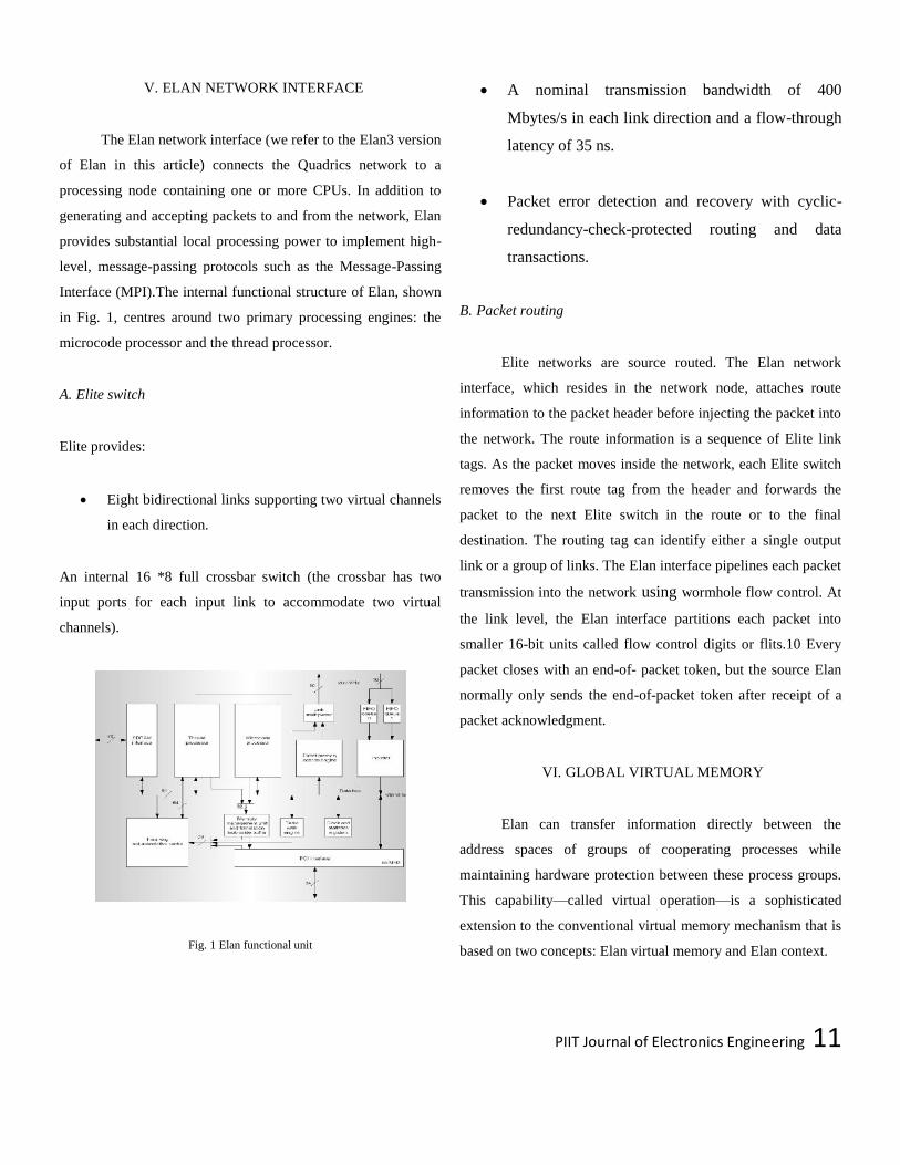
Interface (MPI).The internal functional structure of Elan, shown
in Fig. 1, centres around two primary processing engines: the
microcode processor and the thread processor.
A. Elite switch
Elite provides:
Eight bidirectional links supporting two virtual channels
in each direction.
An internal 16 *8 full crossbar switch (the crossbar has two
input ports for each input link to accommodate two virtual
channels).
Fig. 1 Elan functional unit
A nominal transmission bandwidth of 400
Mbytes/s in each link direction and a flow-through
latency of 35 ns.
Packet error detection and recovery with cyclic-
redundancy-check-protected routing and data
transactions.
B. Packet routing
Elite networks are source routed. The Elan network
interface, which resides in the network node, attaches route
information to the packet header before injecting the packet into
the network. The route information is a sequence of Elite link
tags. As the packet moves inside the network, each Elite switch
removes the first route tag from the header and forwards the
packet to the next Elite switch in the route or to the final
destination. The routing tag can identify either a single output
link or a group of links. The Elan interface pipelines each packet
transmission into the network using wormhole flow control. At
the link level, the Elan interface partitions each packet into
smaller 16-bit units called flow control digits or flits.10 Every
packet closes with an end-of- packet token, but the source Elan
normally only sends the end-of-packet token after receipt of a
packet acknowledgment.
VI. GLOBAL VIRTUAL MEMORY
Elan can transfer information directly between the
address spaces of groups of cooperating processes while
maintaining hardware protection between these process groups.
This capability—called virtual operation—is a sophisticated
extension to the conventional virtual memory mechanism that is
based on two concepts: Elan virtual memory and Elan context.
PIIT Journal of Electronics Engineering 12
A.Elan virtual memory
Elan contains an MMU to translate the virtual memory
addresses issued by the various on-chip functional units (thread
processor, DMA engine, and so on) into physical addresses.
These physical memory addresses can refer to either Elan local
memory (SDRAM) or the node‘s main memory. To support
main memory accesses, the configuration tables for the Elan
MMU are synchronized with the main processor‘s MMU tables
so that Elan can access its virtual address space. The system
software is responsible for MMU table synchronization and is
invisible to programmers.
The Elan MMU can translate between virtual addresses in the
main processor format (for example, a 64-bit word, big-endian
architecture, such as that of the Alpha Server) and virtual
addresses written in the Elan format (a 32-bit word, little-endian
architecture). A processor with a 32-bit architecture (for
example, an Intel Pentium) requires only one-to one mapping.
B.Elan context
In a conventional virtual-memory system, each user
process has an assigned process identification number that
selects the MMU table set and, therefore, the physical address
spaces accessible to the user process. QsNet extends this
concept so that the user address spaces in a parallel program can
intersect. Elan replaces the process identification number value
with a context value. User processes can directly access an
exported segment of remote memory using a context value and a
virtual address
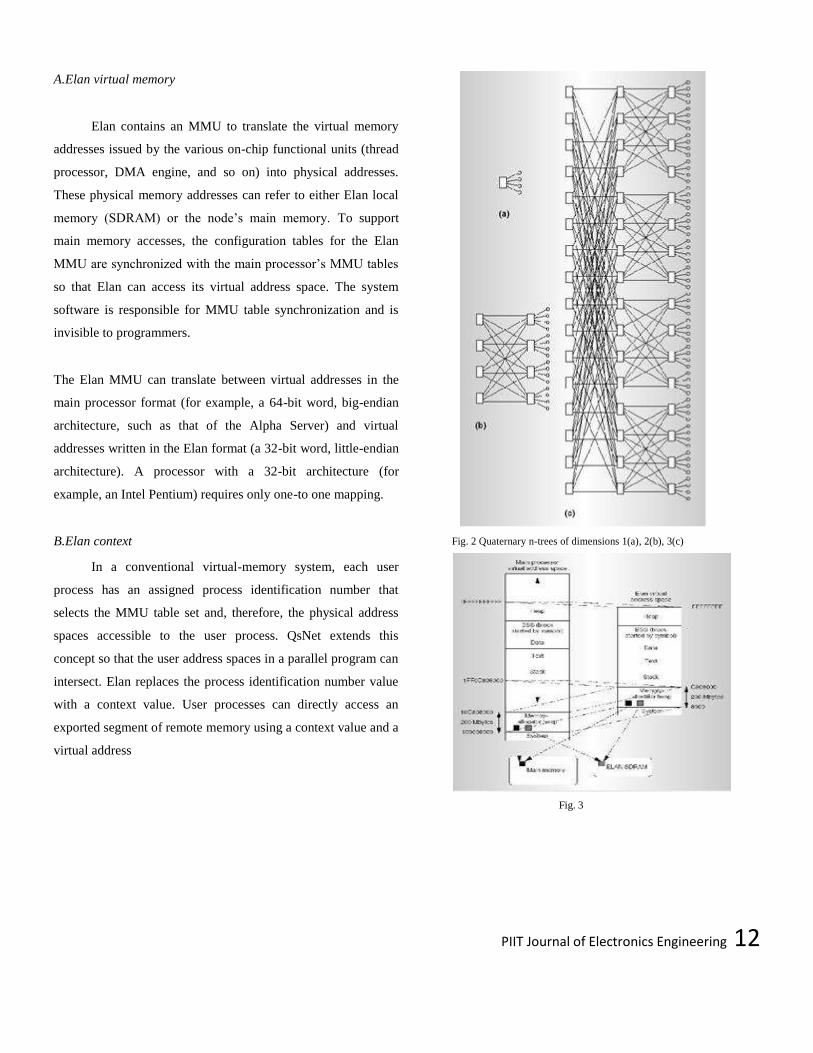
Fig. 2 Quaternary n-trees of dimensions 1(a), 2(b), 3(c)
Fig. 3
PIIT Journal of Electronics Engineering 13
VII. NETWORK FAULT DETECTION AND FAULT TOLERANCE
A. Network fault detection and fault tolerance
QsNet implements network fault detection and tolerance
in hardware. (It is important to note that this fault detection and
tolerance occurs between two communicating Elans). Under
normal operation, the source Elan transmits a packet (that is,
route information for source routing followed by one or more
transactions). When the receiver in the destination Elan receives
a transaction with an ACK Now flag, it means that this
transaction is the last one for the packet. The destination Elan
then sends a packet acknowledgment token back to the source
Elan. Only when the source Elan receives the packet
acknowledgment token does it send an end-of-packet token to
indicate the packet transfer‘s completion. The fundamental rule
of Elan network operation is that for every packet sent down a
link, an Elan interface returns a single packet- acknowledgment
token. The network will not reuse the link until the destination
Elan sends such a token.
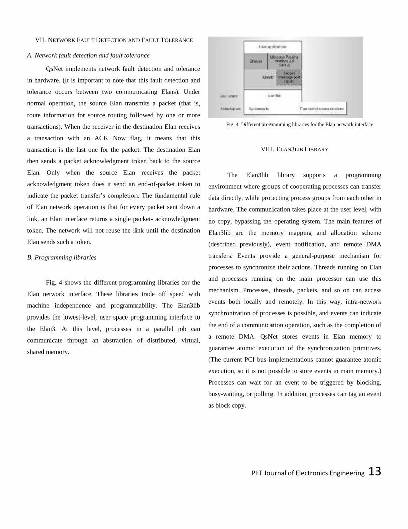
B. Programming libraries
Fig. 4 shows the different programming libraries for the
Elan network interface. These libraries trade off speed with
machine independence and programmability. The Elan3lib
provides the lowest-level, user space programming interface to
the Elan3. At this level, processes in a parallel job can
communicate through an abstraction of distributed, virtual,
shared memory.
Fig. 4 Different programming libraries for the Elan network interface
VIII. ELAN3LIB LIBRARY
The Elan3lib library supports a programming
environment where groups of cooperating processes can transfer
data directly, while protecting process groups from each other in
hardware. The communication takes place at the user level, with
no copy, bypassing the operating system. The main features of
Elan3lib are the memory mapping and allocation scheme
(described previously), event notification, and remote DMA
transfers. Events provide a general-purpose mechanism for
processes to synchronize their actions. Threads running on Elan
and processes running on the main processor can use this
mechanism. Processes, threads, packets, and so on can access
events both locally and remotely. In this way, intra-network
synchronization of processes is possible, and events can indicate
the end of a communication operation, such as the completion of
a remote DMA. QsNet stores events in Elan memory to
guarantee atomic execution of the synchronization primitives.
(The current PCI bus implementations cannot guarantee atomic
execution, so it is not possible to store events in main memory.)
Processes can wait for an event to be triggered by blocking,
busy-waiting, or polling. In addition, processes can tag an event
as block copy.
PIIT Journal of Electronics Engineering 14
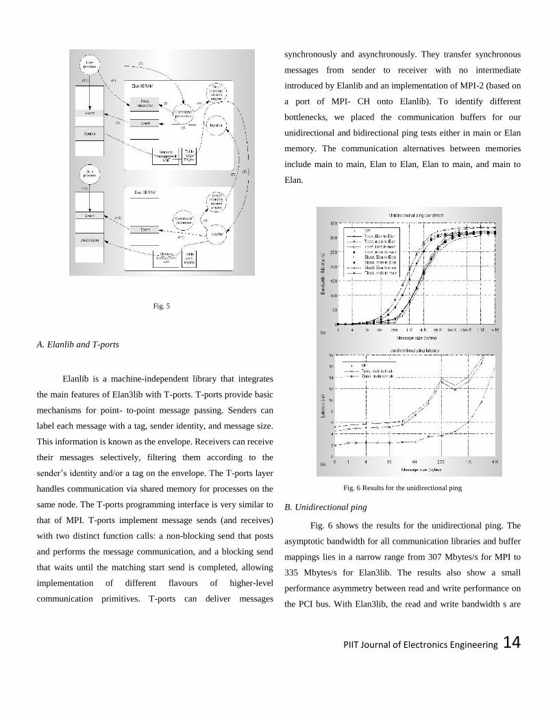
Fig. 5
A. Elanlib and T-ports
Elanlib is a machine-independent library that integrates
the main features of Elan3lib with T-ports. T-ports provide basic
mechanisms for point- to-point message passing. Senders can
label each message with a tag, sender identity, and message size.
This information is known as the envelope. Receivers can receive
their messages selectively, filtering them according to the
sender‘s identity and/or a tag on the envelope. The T-ports layer
handles communication via shared memory for processes on the
same node. The T-ports programming interface is very similar to
that of MPI. T-ports implement message sends (and receives)
with two distinct function calls: a non-blocking send that posts
and performs the message communication, and a blocking send
that waits until the matching start send is completed, allowing
implementation of different flavours of higher-level
communication primitives. T-ports can deliver messages
synchronously and asynchronously. They transfer synchronous
messages from sender to receiver with no intermediate
introduced by Elanlib and an implementation of MPI-2 (based on
a port of MPI- CH onto Elanlib). To identify different
bottlenecks, we placed the communication buffers for our
unidirectional and bidirectional ping tests either in main or Elan
memory. The communication alternatives between memories
include main to main, Elan to Elan, Elan to main, and main to
Elan.
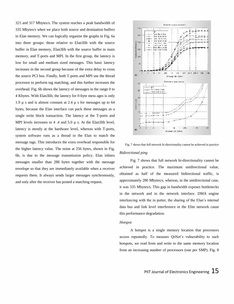
Fig. 6 Results for the unidirectional ping
B. Unidirectional ping
Fig. 6 shows the results for the unidirectional ping. The
asymptotic bandwidth for all communication libraries and buffer
mappings lies in a narrow range from 307 Mbytes/s for MPI to
335 Mbytes/s for Elan3lib. The results also show a small
performance asymmetry between read and write performance on
the PCI bus. With Elan3lib, the read and write bandwidth s are
PIIT Journal of Electronics Engineering 15
321 and 317 Mbytes/s. The system reaches a peak bandwidth of
335 Mbytes/s when we place both source and destination buffers
in Elan memory. We can logically organize the graphs in Fig. 6a
into three groups: those relative to Elan3lib with the source
buffer in Elan memory, Elan3lib with the source buffer in main
memory, and T-ports and MPI. In the first group, the latency is
low for small and medium sized messages. This basic latency
increases in the second group because of the extra delay to cross
the source PCI bus. Finally, both T-ports and MPI use the thread
processor to perform tag matching, and this further increases the
overhead. Fig. 6b shows the latency of messages in the range 0 to
4 Kbytes. With Elan3lib, the latency for 0-byte mess ages is only
1.9 µ s and is almost constant at 2.4 µ s for messages up to 64
bytes, because the Elan interface can pack these messages as a
single write block transaction. The latency at the T-ports and
MPI levels increases to 4 .4 and 5.0 µ s. At the Elan3lib level,
latency is mostly at the hardware level, whereas with T-ports,
system software runs as a thread in the Elan to match the
message tags. This introduces the extra overhead responsible for
the higher latency value. The noise at 256 bytes, shown in Fig.
6b, is due to the message transmission policy. Elan inlines
messages smaller than 288 bytes together with the message
envelope so that they are immediately available when a receiver
requests them. It always sends larger messages synchronously,
and only after the receiver has posted a matching request.
Fig. 7 shows that full network bi-directionality cannot be achieved in practice
Bidirectional ping
Fig. 7 shows that full network bi-directionality cannot be
achieved in practice. The maximum unidirectional value,
obtained as half of the measured bidirectional traffic, is
approximately 280 Mbytes/s, whereas, in the unidirectional case,
it was 335 Mbytes/s. This gap in bandwidth exposes bottlenecks
in the network and in the network interface. DMA engine
interleaving with the in putter, the sharing of the Elan‘s internal
data bus and link level interference in the Elite network cause
this performance degradation.
Hotspot
A hotspot is a single memory location that processors
access repeatedly. To measure QsNet‘s vulnerability to such
hotspots, we read from and write to the same memory location
from an increasing number of processors (one per SMP). Fig. 8

PIIT Journal of Electronics Engineering 16
(next page) plots bandwidth for increasing numbers of SMPs.
The upper curve of this figure shows the aggregate global
bandwidth for all processes. The curves are remarkably flat,
reaching 314 and 307 M bytes/s for read and write hotspots. The
lower curves show the per-SMP band- Bandwidth. The
scalability of this type of memory operation is very good, up to
the available number of processors in our cluster.
IX. CONCLUSION
While there are certainly a number of differences between
embedded clusters and standard clusters that have been brought
out in this section, there are also a number of similarities, and in
many ways, the two types of clusters are converging. Mass-
market forces and the need for software portability are driving
embedded clusters to use similar operating systems, tools, and
inter-connects as standard clusters. As traditional clusters grow
in size and complexity, there is a growing need to use denser
packaging techniques and higher bandwidth, lower latency
interconnects. Real- time capability is also becoming more
common in traditional clusters in industrial applications,
particularly as clusters become more interactive, both with
people and with other hardware. Additionally, fault-tolerance is
becoming more important for standard clusters: first, as they are
increasingly accepted into machine rooms and subject to
reliability and up-time requirements.
X. FUTURE WORK
As SMP become more common in clusters, we will see a
natural hierarchy arise. SMP have tight coupling, and will be
joined into clusters via low-latency high- bandwidth
interconnection networks. Indeed, we fully expect that
heterogeneous clusters of SMP will arise, having single, dual,
quad, and octo-processor boxes in the same cluster. These
clusters will, in turn, be joined by gigabit-speed wide-area
networks, which will differ from SAN primarily in their latency
characteristics. This environment will naturally have a three-level
hierarchy, with each level having an order of magnitude
difference in latency relative to the next layer.
This structure will have its greatest impact on scheduling,
both in terms of task placement and in terms of selecting a
process to run from a ready queue. Scheduling is traditionally
considered an operating system activity, yet it is quite likely that
at least some of this work will be carried out in middleware.
For example, as one of our research projects we are
investigating thread management for mixed-mode (multi-
threaded and message passing) computing using OpenMP and
MPI, which we believe is a natural by-product of clusters of
SMP. Most cluster applications, particularly scientific
computations traditionally solved via spatial decomposition,
consist of multiple cooperating tasks. During the course of the
computation, hot spots will arise, and a self-adapting program
might wish to manage the number of active threads it has in each
process. Depending on the relationship of new threads to existing
threads (and their communication pattern) and the system state, a
decision might be made to do one of the following:
Add a new thread on an idle processor of the SMP where
the process is already running.
Expand the address space via distributed shared memory
to include an additional node, and add a thread there.
Add a thread to a non-idle processor already assigned to
the process.
Migrate the process to a larger SMP (e.g. from 2 nodes
to 4 nodes) with an idle processor, and add a new thread
there.
REFERENCES
[1]R.Seifert, Gigabit Ethernet: Technology and Applications for High
Speed LANs, Addison Wesley, Reading, Mass., 1998.
[2]W. Vogels et al., ―Tree-Saturation Control in the AC3 Velocity
Cluster", Hot Interconnects vogels/clusters/ac3/hoti_files/frame.htm
(current Dec. 2001).

PIIT Journal of Electronics Engineering 17
[3]H. Hellwagner, ―The SCI Standard and Applications of SCI, ‖ SCI:
Scalable Coherent Interface, Lecture Notes in Computer Science, vol.
1291, H. Hellwagner and A. Reinfeld, eds., Springer-Verlag,
Heidelberg, Germany, 1999, pp. 95-116.
[4]N.J. Boden et al., ―Myrinet: A Gigabit-per- Second Local Area
Network, ‖ IEEE Micro, vol. 15, no. 1, Jan. 1995, pp. 29-36.

PIIT Journal of Electronics Engineering 18
Automated Design of Robust PID Controller Using
Genetic Algorithm
Patel Iftekar
Department of Electronics
Engineering
PIIT, New Panvel.
Prof.Monika Bhagwat
Department of Electronics
Engineering
PIIT, New Panvel.
Prof.Ujwal Harode
Department of Electronics
Engineering
PIIT, New Panvel.
Abstract—the paper deals with the design of robust
controller for uncertain SISO systems using Quantitative
Feedback Theory (QFT) and optimization of controller
being done with the help of Genetic Algorithm (GA).
Quantitative Feedback Theory (QFT) technique is a robust
control design based on frequency domain methodology. It is
useful for practical design of feedback system in ensuring
plant’s stability by reducing the sensitivity to parameter
variation and attenuates the effect of disturbances.
Parameter variation or physical changes to the plant is
taken into account in the QFT controller’s design.
Quantitative Feedback Theory (QFT) can provide robust
control for the plant with large uncertainties. The manual
design with the help of QFT toolbox in Matlab is
complicated and even unsolvable. The existing automatic
design methods are limited in optimization. Based on the
genetic algorithm (GA), a more effective automatic design
methodology of QFT robust controller is proposed. Some
new optimization indexes like IAE, ISE, ITAE and MSE are
adopted, so the design method is more mature. To obtain
good performance of the controller in a relatively short time,
the manual design and the automatic design are combined.
Compared with the results from the manual design method,
the performance of the QFT controller based on genetic
algorithms is better and the efficiency of searching scheme is
the best. An illustrative example which compares manual
loop shaping with automatic loop shaping is given.
Keywords—Robust controller, Quantitative Feedback
Theory (QFT), Genetic Algorithm(GA), Uncertainties,
stability, Manual loop shaping, Automatic loop shaping,
Optimization index, Matlab , Mean of the Squared Error
(MSE), Integral of Time multiplied by Absolute Error (ITAE),
Integral of Absolute Magnitude of the Error (IAE), Integral of
the Squared Error (ISE).
I.INTRODUCTION
There are two general control systems. (i) Conventional
control, and (ii) Robust control, which typically involves worst
case design approach for family of plants using a single fixed
controller [1]. If the design performs well for substantial
variations in the dynamics of the plant from the design values,
then the design is robust. Robust control deals explicitly with
uncertainty in its approach to controller design. Controllers
designed using robust control methods tend to be able to cope
with small differences between the true system and the nominal
model used for design. Quantitative Feedback Theory (QFT) is
robust control method which deals with the effects of

PIIT Journal of Electronics Engineering 19
uncertainty systematically. QFT is a graphical loop shaping
procedure used for the control design of either SISO (Single
Input Single Output) or MIMO (Multiple Input Multiple Output)
uncertain systems including the nonlinear and time varying
cases. QFT, developed by Isaac Horowitz is a frequency
domain technique utilizing the Nichols chart (NC) in order to
achieve a desired robust design over a specified region of plant
uncertainty. In comparison to other robust control methods, QFT
offers a number of advantages. For the purpose of QFT, the
feedback system is normally described by the two-degrees- of
freedom structure. [3]
A proportional–integral–derivative controller (PID
Controller) is a generic control loop feedback mechanism widely
used in industrial control systems. PID controllers have
dominated the process control industry over the decades owing to
its associated simplicity and easiness in implementation. The
design of PID controllers, tuning involves selecting the
amounts of Proportional, Integral and Derivative components
required at the output of the controller. Since the design of PID
controllers involves obtaining the P, I and D components there
always occurs a compromise in the design. The design of the
optimum values for the PID controller parameters has always
been challenging. Many new tuning techniques have been
developed for the design of PID controllers, however then still
exists a scope for better tuning method. Various control strategies
are used for design of control system depending on plant model.
[4]
One of the most frequently used on-line tuning methods is the
Genetic Algorithm (GA). The genetic algorithm is very effective
at finding optimal solutions to a variety of problems. This
innovative technique performs especially well when solving
complex problems because it doesn't impose many limitations of
traditional techniques. Due to its evolutionary nature, a GA will
search for solutions without regard to the specific inner working
of the problem. This ability lets the same general purpose GA
routine perform well on large, complex scheduling problems.
There is now considerable evidence that genetic algorithms are
useful for global function optimization.
II.LITERATURE REVIEW
Quantitative Feedback Theory (QFT) has been applied in
many engineering systems successfully since it was develop
In [7], Qingwei Wang, Zhenghua Liu, Lianjie Er presented
automatic design method of QFT controller based on GA and
proposed several initial optimization indexes to make the
controller more practical. They proved that GA based automatic
design method of QFT controller is very effective and
optimization method can achieve both high performance and
increased efficiency.
In [8], A Zolotas and G.D Halikias proposed an
optimization algorithm for designing PID controllers, which
minimizes the asymptotic open-loop gain of a system, subject to
appropriate robust stability and performance QFT constraints.
The algorithm is simple and can be used to automate the loop-
shaping step of the QFT design procedure. The effectiveness of
the method is illustrated with an example.
In [6], Wenhua Chen and Donald J. Balance addressed design
of robust controllers for uncertain and non-minimum phase and
unstable plant using QFT technique. Benchmark examples were
used to illustrate the improved method
In [11], Mario Garcia-Saenz In the first part of the paper
summarized the main concepts of the Quantitative Feedback
Theory (QFT) and presented a wide set of references related to
the principal areas of research. In the second part of the paper
introduced a method to design non-diagonal QFT controllers for
MIMO systems. Finally the paper ends presenting some real-
world applications of the technique, carried out by the author: an
industrial SCARA robot manipulator, a wastewater treatment
plant of 5000 m3/hour, a variable speed pitch controlled
multipolar wind turbine of 1.65 MW and an industrial furnace of
40 meters and 1 MW.

PIIT Journal of Electronics Engineering 20
In [10], O. Yana and M. Mazurka examined an analytically-
based algorithm for finding low order controllers that satisfy
closed loop gain and phase margin constraints and a bound on
the sensitivity.
In [14], K. Krishna Kumar and D. E. Goldberg proposed an
approach which improves the quality and speed of manual loop
shaping; Genetic Algorithm was used to provide global
optimization.
In [16], P.S.V.NATRAJ Proposed an algorithm for
generating QFT bounds to achieve robust tracking specifications.
The proposed algorithm can generate tracking bounds over
intervals of controller phase values, as opposed to discrete
controller phase values in existing algorithms.
BASICS OF PID CONTROL SYSTEM
PID controller consists of the three terms: proportional (P)
integral (I), and derivative (D). Its behavior can be roughly
interpreted as the sum of the three term actions The P term gives
a rapid control response and a possible steady state error, the I
term eliminates the steady state error and the D term improves
the behavior of the control system during transients.[4]
The Transfer function of PID controller is given b Where Kp
= Gain of the system.
Ti = Integral time constant.
Td = Derivative time constant
Fig. 1 parallel form of PID
III.QFT BASIC CONCEPTS
QFT is a very powerful control system design method when
the Plant parameters vary over a broad range of operating
conditions. The basic concept of QFT is to define and take into
account, along the control design process, the quantitative
Relation between the amount of uncertainty to deal with and the
amount of control effort to use. The Quantitative Feedback
Theory (QFT) method offers, frequency-domain based design
approach for tackling feedback control problems with robust
performance objectives.[3] In this approach, the plant Dynamics
may be described by frequency response data, or by a transfer
function with mixed (parametric and nonparametric) Uncertainty
models. The basic idea in QFT is to convert design specifications
at closed loop and plant uncertainties into robust stability and
performance bounds on open loop transmission of nominal
system and then design controller by using loop shaping [5]. The
two-degree-freedom feedback system configuration of QFT is
given in Fig.1.
Fig. 2 QFT Configuration, where G(s) - Controller, F(s) - pre-filter,
P(s) - uncertain plant which belongs to a given plant family Ƥ.
IV.CONTROLLER DESIGN PROCEDURE USING QFT
Design Steps for PID Controller are as follows:
1. Translation of TDS to FDS (Time Domain Specification
to Frequency Domain Specification).
2. Generation of the Plant Set.
3. Generation of the Template.
4. Grouping of Bounds.
5. Intersections of Bounds.
6. Loop shaping (Design of a Controller).
7. Pre-filter Designs.
PIIT Journal of Electronics Engineering 21
V.DESIGN EXAMPLE
A Benchmark example from QFT toolbox is
considered in order to explain the various design steps
QFT controller.
Consider a plant with parametric uncertainty given by:
P(s) = : k ϵ [1, 10], a ϵ [1, 10]
The stability index is given by:
, ω > 0,
And upper and lower boundaries of tracking index are,
TU (ω) ≤
≤ TL (ω)
Where TU (ω) =
and TL (ω) =
And output disturbance rejection bound is given by
Translation from TDS to FDS (Time Domain Specification to
Frequency Domain Specification)
Since a benchmark example from QFT TOOLBOX is
considered in this paper, the specifications are readily available
in frequency domain.
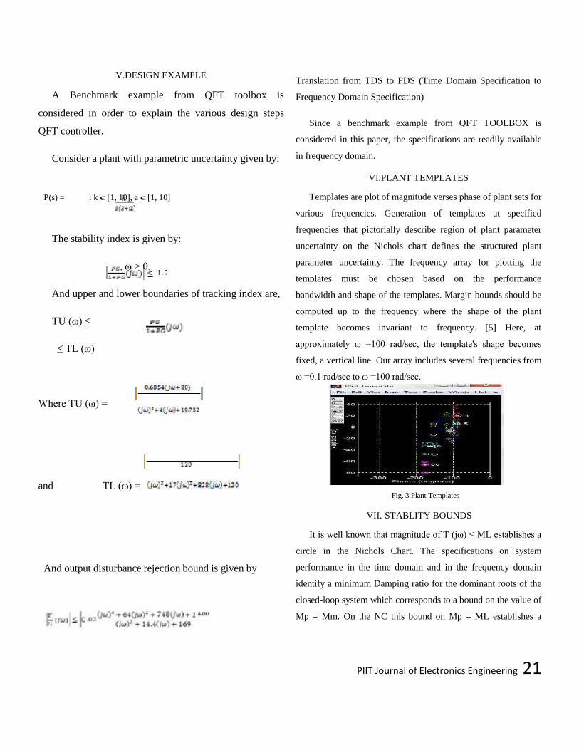
VI.PLANT TEMPLATES
Templates are plot of magnitude verses phase of plant sets for
various frequencies. Generation of templates at specified
frequencies that pictorially describe region of plant parameter
uncertainty on the Nichols chart defines the structured plant
parameter uncertainty. The frequency array for plotting the
templates must be chosen based on the performance
bandwidth and shape of the templates. Margin bounds should be
computed up to the frequency where the shape of the plant
template becomes invariant to frequency. [5] Here, at
approximately ω =100 rad/sec, the template's shape becomes
fixed, a vertical line. Our array includes several frequencies from
ω =0.1 rad/sec to ω =100 rad/sec.
Fig. 3 Plant Templates
VII. STABLITY BOUNDS
It is well known that magnitude of T (jω) ≤ ML establishes a
circle in the Nichols Chart. The specifications on system
performance in the time domain and in the frequency domain
identify a minimum Damping ratio for the dominant roots of the
closed-loop system which corresponds to a bound on the value of
Mp = Mm. On the NC this bound on Mp = ML establishes a
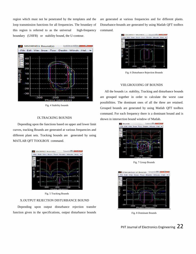
PIIT Journal of Electronics Engineering 22
region which must not be penetrated by the templates and the
loop transmission functions for all frequencies. The boundary of
this region is referred to as the universal high-frequency
boundary (UHFB) or stability bound, the U-contour.
Fig. 4 Stability bounds
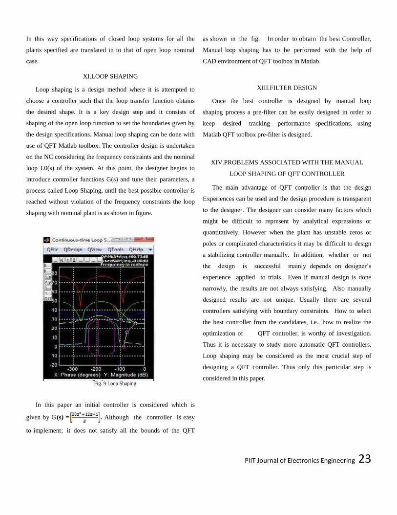
IX.TRACKING BOUNDS
Depending upon the functions based on upper and lower limit
curves, tracking Bounds are generated at various frequencies and
different plant sets. Tracking bounds are generated by using
MATLAB QFT TOOLBOX command.
Fig. 5 Tracking Bounds
X.OUTPUT REJECTION DISTURBANCE BOUND
Depending upon output disturbance rejection transfer
function given in the specifications, output disturbance bounds
are generated at various frequencies and for different plants.
Disturbance-bounds are generated by using Matlab QFT toolbox
command.
Fig. 6 Disturbance Rejection Bounds
VIII.GROUOING OF BOUNDS
All the bounds i.e. stability, Tracking and disturbance bounds
are grouped together in order to calculate the worst case
possibilities. The dominant ones of all the three are retained.
Grouped bounds are generated by using Matlab QFT toolbox
command. For each frequency there is a dominant bound and is
shown in intersection bound window of Matlab.
Fig. 7 Group Bounds
Fig. 8 Dominant Bounds
PIIT Journal of Electronics Engineering 23
In this way specifications of closed loop systems for all the
plants specified are translated in to that of open loop nominal
case.
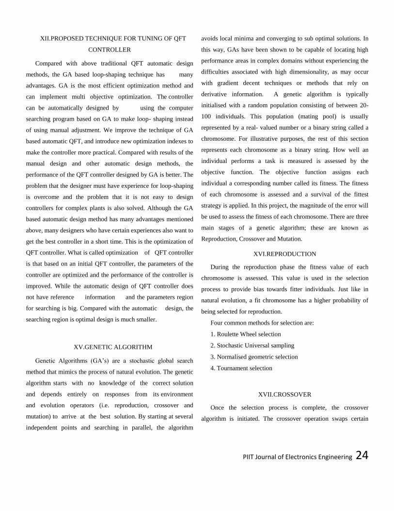
XI.LOOP SHAPING
Loop shaping is a design method where it is attempted to
choose a controller such that the loop transfer function obtains
the desired shape. It is a key design step and it consists of
shaping of the open loop function to set the boundaries given by
the design specifications. Manual loop shaping can be done with
use of QFT Matlab toolbox. The controller design is undertaken
on the NC considering the frequency constraints and the nominal
loop L0(s) of the system. At this point, the designer begins to
introduce controller functions G(s) and tune their parameters, a
process called Loop Shaping, until the best possible controller is
reached without violation of the frequency constraints the loop
shaping with nominal plant is as shown in figure.
Fig. 9 Loop Shaping
In this paper an initial controller is considered which is
given by G(s) = . Although the controller is easy
to implement; it does not satisfy all the bounds of the QFT
as shown in the fig. In order to obtain the best Controller,
Manual loop shaping has to be performed with the help of
CAD environment of QFT toolbox in Matlab.
XIII.FILTER DESIGN
Once the best controller is designed by manual loop
shaping process a pre-filter can be easily designed in order to
keep desired tracking performance specifications, using
Matlab QFT toolbox pre-filter is designed.
XIV.PROBLEMS ASSOCIATED WITH THE MANUAL
LOOP SHAPING OF QFT CONTROLLER
The main advantage of QFT controller is that the design
Experiences can be used and the design procedure is transparent
to the designer. The designer can consider many factors which
might be difficult to represent by analytical expressions or
quantitatively. However when the plant has unstable zeros or
poles or complicated characteristics it may be difficult to design
a stabilizing controller manually. In addition, whether or not
the design is successful mainly depends on designer‘s
experience applied to trials. Even if manual design is done
narrowly, the results are not always satisfying. Also manually
designed results are not unique. Usually there are several
controllers satisfying with boundary constraints. How to select
the best controller from the candidates, i.e., how to realize the
optimization of QFT controller, is worthy of investigation.
Thus it is necessary to study more automatic QFT controllers.
Loop shaping may be considered as the most crucial step of
designing a QFT controller. Thus only this particular step is
considered in this paper.
PIIT Journal of Electronics Engineering 24
XII.PROPOSED TECHNIQUE FOR TUNING OF QFT
CONTROLLER
Compared with above traditional QFT automatic design
methods, the GA based loop-shaping technique has many
advantages. GA is the most efficient optimization method and
can implement multi objective optimization. The controller
can be automatically designed by using the computer
searching program based on GA to make loop- shaping instead
of using manual adjustment. We improve the technique of GA
based automatic QFT, and introduce new optimization indexes to
make the controller more practical. Compared with results of the
manual design and other automatic design methods, the
performance of the QFT controller designed by GA is better. The
problem that the designer must have experience for loop-shaping
is overcome and the problem that it is not easy to design
controllers for complex plants is also solved. Although the GA
based automatic design method has many advantages mentioned
above, many designers who have certain experiences also want to
get the best controller in a short time. This is the optimization of
QFT controller. What is called optimization of QFT controller
is that based on an initial QFT controller, the parameters of the
controller are optimized and the performance of the controller is
improved. While the automatic design of QFT controller does
not have reference information and the parameters region
for searching is big. Compared with the automatic design, the
searching region is optimal design is much smaller.
XV.GENETIC ALGORITHM
Genetic Algorithms (GA‘s) are a stochastic global search
method that mimics the process of natural evolution. The genetic
algorithm starts with no knowledge of the correct solution
and depends entirely on responses from its environment
and evolution operators (i.e. reproduction, crossover and
mutation) to arrive at the best solution. By starting at several
independent points and searching in parallel, the algorithm
avoids local minima and converging to sub optimal solutions. In
this way, GAs have been shown to be capable of locating high
performance areas in complex domains without experiencing the
difficulties associated with high dimensionality, as may occur
with gradient decent techniques or methods that rely on
derivative information. A genetic algorithm is typically
initialised with a random population consisting of between 20-
100 individuals. This population (mating pool) is usually
represented by a real- valued number or a binary string called a
chromosome. For illustrative purposes, the rest of this section
represents each chromosome as a binary string. How well an
individual performs a task is measured is assessed by the
objective function. The objective function assigns each
individual a corresponding number called its fitness. The fitness
of each chromosome is assessed and a survival of the fittest
strategy is applied. In this project, the magnitude of the error will
be used to assess the fitness of each chromosome. There are three
main stages of a genetic algorithm; these are known as
Reproduction, Crossover and Mutation.
XVI.REPRODUCTION
During the reproduction phase the fitness value of each
chromosome is assessed. This value is used in the selection
process to provide bias towards fitter individuals. Just like in
natural evolution, a fit chromosome has a higher probability of
being selected for reproduction.
Four common methods for selection are:
1. Roulette Wheel selection
2. Stochastic Universal sampling
3. Normalised geometric selection
4. Tournament selection
XVII.CROSSOVER
Once the selection process is complete, the crossover
algorithm is initiated. The crossover operation swaps certain

PIIT Journal of Electronics Engineering 25
parts of the two selected strings in a bid to capture the good parts
of old chromosomes and create better new ones. Genetic
operators manipulate the characters of a chromosome directly,
using the assumption that certain individual‘s gene codes, on
average, produce fitter individuals. Following are the three
crossover techniques:
1. Single-Point Crossover.
2. Multi-Point Crossover.
3. Uniform Crossover.
XVIII.MUTATION
Using selection and crossover on their own will generate a
large amount of different strings. However there are two main
problems with this:
1. Depending on the initial population chosen, there may not
be enough diversity in the initial strings to ensure the GA
searches the entire problem space.
2. The GA may converge on sub-optimum strings due to a
bad choice of initial population.
These problems may be overcome by the introduction of a
mutation operator into the GA. Mutation is the occasional
random alteration of a value of a string position. It is considered
a background operator in the genetic algorithm. The probability
of mutation is normally low because a high mutation rate would
destroy fit strings and degenerate the genetic algorithm into a
random search. Mutation probability values of around 0.1% or
0.01% are common, these values represent the probability that a
certain string will be selected for mutation i.e. for a probability of
0.1%; one string in one thousand will be selected for mutation.
XIX.ELITISM
With crossover and mutation taking place, there is a high risk
that the optimum solution could be lost as there is no guarantee
that these operators will preserve the fittest string. To counteract
this, elitist models are often used. In an elitist model, the best
individual from a population is saved before any of these
operations take place. After the new population is formed and
evaluated, it is examined to see if this best structure has
been preserved. If not, the saved copy is reinserted back into the
population. The GA then continues on as normal.
The steps involved in creating and implementing a genetic
algorithm are as follows:
1. Generate an initial, random population of individuals for a
fixed size.
2. Evaluate their fitness.
3. Select the fittest members of the population.
4. Reproduce using a probabilistic method (e.g., roulette
wheel).
5. Implement crossover operation on the reproduced
chromosomes (Choosing probabilistically both the crossover
site and the ‗mates‘).
6. Execute mutation operation with low probability.
7. Repeat step 2 until a predefined convergence criterion is
met.
XX.TERMINATION
This generational process is repeated until a termination
condition has been reached. Common terminating conditions are:
1. A solution is found that satisfies minimum criteria.
2. Fixed number of generations reached.
3. Allocated budget (computation time/money) reached.
4. The highest ranking solution's fitness is reaching or has
Reached a plateau such that successive iterations no
Longer produce better results.
5. Manual inspection.
6. Combinations of the above.

PIIT Journal of Electronics Engineering 26
XXI.USING THE OPTIMIZATION TOOL
To open the Optimization Tool, enter Optimtool ('ga') at the
command line, or enter optimtool and then choose ga from the
Solver menu.
To use the Optimization Tool, you must first enter the
following information:
XXII.FITNESS FUNCTION
The objective function you want to minimize. Enter the
fitness function in the form @fitnessfun, where fitnessfun.m is a
file that computes the fitness function. The @ sign creates a
function handle to fitnessfun. Writing an objective function is the
most difficult part of creating a genetic algorithm. In this paper,
the objective function is required to evaluate the best PID
controller for the DC Motor. An objective function could be
created to find a PID controller that gives the smallest overshoot,
fastest rise time or quickest settling time but in order to combine
all of these objectives it was decided to design an objective
function that will minimise the error of the controlled system.
Each chromosome in the population is passed into the objective
function one at a time. The chromosome is then evaluated and
assigned a number to represent its fitness, the bigger its number
the better its fitness. The genetic algorithm uses the
chromosome‘s fitness value to create a new population consisting
of the fittest members.
In this paper the objective function is defined by various
Error Performance Criterion such as MSE, ITAE, ISE, and IAE.
The controlled system is given a step input and the error is
assessed using an appropriate error performance criterion i.e.
ITAE, ISE, IAE or MSE. The chromosome is assigned an overall
fitness value according to the magnitude of the error, the smaller
the error the larger the fitness value. The above mentioned
objective functions are specified with the help of a code in a
Matlab file and it is then called appropriately from the objective
functions pane.
XXIII.NUMBER OF VARIABLES
The length of the input vector to the fitness function is
defined by number of variables. In this paper the number of
variables are 3 i.e. Kp, Z1, Z2.
XXIV.CONVERSION OF QFT BOUNDS INTO
QUADRATIC INEQUALITIES OR GA CONSTRAINTS
You can enter constraints or a nonlinear
constraint function for the problem in the Constraints pane.
If the problem is unconstrained, leave these fields blank.
(1) Stability bound given by
is converted to a quadratic inequality given by
(2) Disturbance bound given by
is converted to a quadratic inequality given by
(3) Tracking bound given by
PIIT Journal of Electronics Engineering 27
Is converted to a quadratic inequality by
The above derived constraints are specified with the help
of a code in a Matlab file and it is then called
appropriately from the constraints pane.
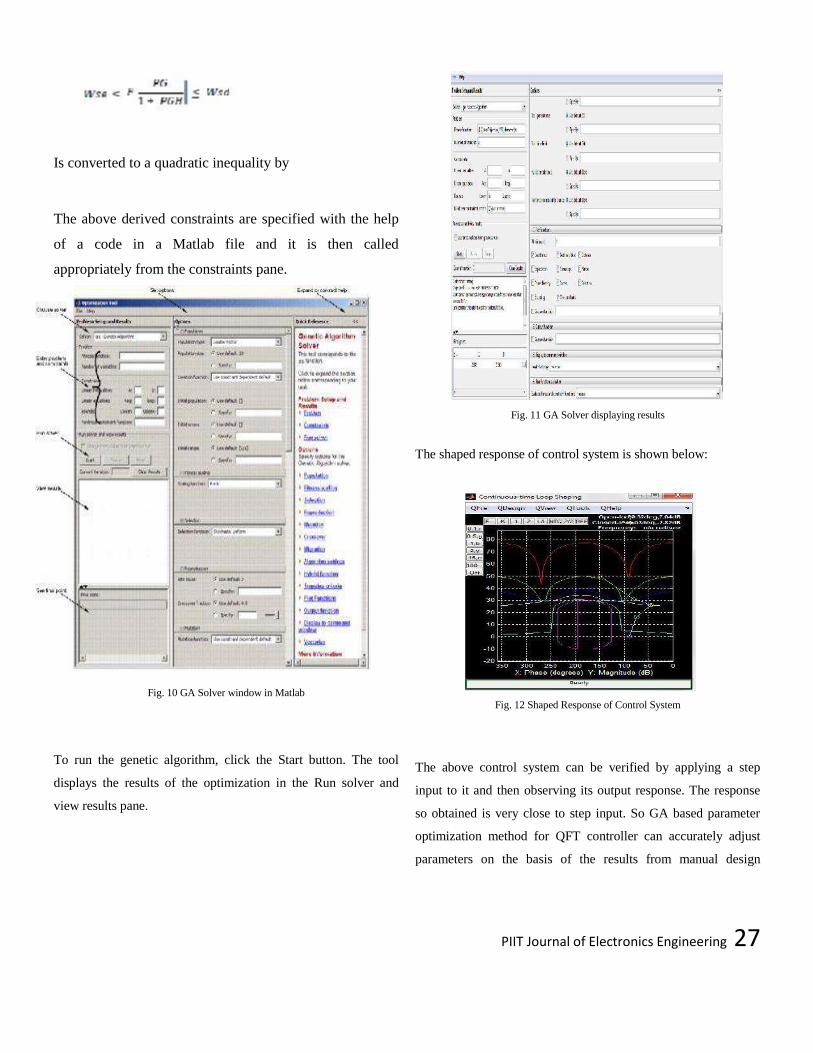
Fig. 10 GA Solver window in Matlab
To run the genetic algorithm, click the Start button. The tool
displays the results of the optimization in the Run solver and
view results pane.
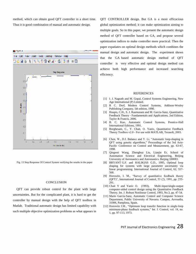
Fig. 11 GA Solver displaying results
The shaped response of control system is shown below:
Fig. 12 Shaped Response of Control System
The above control system can be verified by applying a step
input to it and then observing its output response. The response
so obtained is very close to step input. So GA based parameter
optimization method for QFT controller can accurately adjust
parameters on the basis of the results from manual design
PIIT Journal of Electronics Engineering 28
method, which can obtain good QFT controller in a short time.
Thus it is good combination of manual and automatic design.
Fig. 13 Step Response Of Control System verifying the results in the paper
CONCLUSION
QFT can provide robust control for the plant with large
uncertainties. But for the complicated plant, it is hard to get the
controller by manual design with the help of QFT toolbox in
Matlab. Traditional automatic design has limited capability with
such multiple objective optimization problems as what appears in
QFT CONTROLLER design. But GA is a more efficacious
global optimization method; it can make optimization aiming to
multiple goals. So in this paper, we present the automatic design
method of QFT controller based on GA, and propose several
optimization indices to make controller more practical. Then the
paper expatiates on optimal design methods which combines the
manual design and automatic design. The experiment shows
that the GA based automatic design method of QFT
controller is very effective and optimal design method can
achieve both high performance and increased searching
efficiency.
REFERENCES
[1] I. J. Nagrath and M. Gopal, Control Systems Engineering, New Age International (P) Limited.
[2] R C. Dorf, Modern Control Systems, Addison-Wesley Publishing Company, 5th edition, 1990.
[3] Houpis, C.H., S. J. Rasmussen and M. Garcia-Sanz, Quantitative
Feedback Theory - Fundamentals and Applications, 2nd Edition,
Taylor & Francis, 2006.
[4] B. C. Kuo, Automatic Control Systems, Prentice-Hall
International Editions, 1991.
[5] Borghesani, C., Y. Chait, O. Yaniv, Quantitative Feedback
Theory Toolbox v2.0 - For use with MATLAB, Terasoft, 2003.
[6] Chen, W., D.J. Balance and Y. Li, ―Automatic loop-shaping in
QFT using genetic algorithms,‖ Proceedings of the 3rd Asia-
Pacific Conference on Control and Measurement, pp. 63-67,
1998.
[7] Qingwei Wang, Zhenghua Liu, Lianjie Er, School of
Automation Science and Electrical Engineering, Beijing University of Aeronautics and Astronautics. Beijing 100083.
[8] BRYANT G.F. and HALIKIAS G.D., 1995, Optimal loop
shaping for systems with large parameter uncertainty via
linear programming. International Journal of Control, 62, 557-568.
[9] Horowitz, I. M., ―Survey of quantitative feedback theory
(QFT)‖, International Journal of Control, 53 (2), 1991, pp. 255-
291.
[10] Chait Y and Yaniv O. (1993), Multi-input/single-output
computer-aided control design using the Quantitative Feedback Theory. Int. J. Robust Nonlinear Control, 1993, No.3, pp. 47-54.
[11] Mario Garcia-Sanz, Automatic Control and Computer Science
Department, Public University of Navarra. Campus, Arrosadia, 31006, Pamplona, Spain.
[12] Horowitz I.M., ―Optimum loop transfer function in single-loop
minimum-phase feedback systems,‖ Int. J. Control, vol. 18, no. 1, pp. 97-113, 1973.

PIIT Journal of Electronics Engineering 29
[13] Ibtissem Chiha, 1 Noureddine Liouane, 2 and Pierre Borne3,
Tuning PID Controller Using Multi-objective Ant Colony Optimization.

PIIT Journal of Electronics Engineering 30
DATA ACQUISITION THROUGH GSM
Prof.Meera .B. Kharat
Department of Electronics Engineering
PIIT, New Panvel
Ankur Upadhyay
Department of Electronics Engineering
PIIT, New Panvel
Abstract—The purpose of this device is used for acquiring
data from remote location using PC .The data to be
acquired is collected by micro controller that is installed
at industrial location and is connected to various
machines. The micro controller continuously records
whatever parameters it is programmed to record and
display them on display screen. The micro controller is
also connected to mobile. A PC installed in an office at a
distance location can connect to this micro controller to
mobile. Whenever the data is to be acquired the PC dials
up the number of micro controller line. Once the
connection is made PC sends the command to the micro
controller giving the details of required. The micro
controller then sends the demanded data to the PC .the
data acquired by the micro controller is in digital format
and is stored in EEPROM .The PC automatically
generates the file name and stores data along with the real
time.
1. INTRODUCTION
Data acquisition systems have evolved rapidly in the past few
decades fueled by the advances in electrical computer
engineering and computer science. Standardized input output
interfaces have allowed for the development of peripherals
such as transducers that connect seamlessly to the computer
and make the task of data acquisition a simple one. Data
acquisition systems have become faster and relatively
inexpensive [2]. They have also experienced a reduction in
size and are more reliable. Their high accuracy has made them
an essential tool in a wide range of research areas where
quantitative methods of analysis are required. DAS plays
important role in engineering experiments. Data acquisition
system is the process by which events in the real world are
sampled and translated into machine- readable signals [1].
Sometimes abbreviated DAQ data acquisition typically
involves sensors, transmitters and other instruments to collect
signals, waveforms etc. to be processed and with a computer.
A typical data acquisition system in common use is the data
acquisition card, which can be inserted in the PC main board
and make a PC- based data acquisition system. The first step
in data acquisition is to detect and convert physical
characteristics, such as pressure, temperature, and flow rate,
and position into an electrical signal. This is done using a
transducer is a
Device that converts a physical quantity into an electrical
signal. Transducers have several important properties. One
such property is linearity. Data acquisition systems, as the
name implies, are products and/or processes used to collect
information to document or analyze some phenomenon. In the
simplest form, a technician logging the temperature of an oven
on a piece of paper is performing data acquisition. As
technology has progressed, this type of process has been
simplified and made more accurate, versatile, and reliable
through electronic equipment. Equipment ranges from
simple recorders to sophisticated computer systems [1] [3].
Data acquisition products serve as a focal point in a system,
tying together a wide variety of products, such as sensors that
indicate temperature, flow, level, or pressure.

PIIT Journal of Electronics Engineering 31
II. METHODOLOGY
A. Hardware Description
This system is used to access data from remote location
Using PC the data is to acquire is collected by microcontroller
and it is stored in EEPROM. The data which is stored in
EEPROM is continuously displayed on LCD display. In this
system data acquisition is done by GSM module .When the
person wants to access the data from receiver side one can
directly dial the mobile number present at transmitter side.
Once the number dialed and connection is established
microcontroller will get the signal from DTMF decoder that
call is arrived. Then the microcontroller will send the signal
SOC to ADC and after reading the complete data from ADC it
will send the signal EOC to microcontroller. The
microcontroller then sends the recorded data to PC through
GSM module. PC is interfaced with GSM module through
RS232 port. The same data which is recorded at transmitter
can be seen at receiver on PC. The data can be taken at
regular interval. The data which is to be taken are different
parameters like temperature, voltage, current and frequency.
For temperature sensor is used in the system which will record
the present temperature. For current, current transformer is
used which is applied channel-2 of ADC. For voltage, voltage
transformer is used which is applied channel-1 of ADC.
Frequency input is taken from NAND gate here two NAND
gates are shorted which will act as signal conditioning and
then applied to microcontroller. In this system these four
parameters are recorded at transmitter and these data can be
accessed at receiver by simply dialing the number of
transmitter. Data transmission is done through GSM module.
It‘s a wireless communication system. RTC is also used in this
project so that it will display the time as well when the data is
recorded. Thus the system is use to acquire data from remote
location the data acquire in the system is through GSM.
Block Diagram of Data Acquisition through GSM (Transmitter)
B. System Model
This device is used for acquiring data from a
remote location using a PC[1]. The readings which are
supposed to be recorded are temperature, voltage,
current and frequency. For temperature sensor LM34 IC is
used in the system which will record the present temperature it
is applied to voltage follower and then to channel-0 of ADC
For current, current transformer is used which is applied to
voltage follower and then to channel-2 of ADC . For voltage,
voltage transformer is used which is applied to voltage
follower and to Channel-1 of ADC. The output of all these
parameters is applied to voltage follower so that no leakage in
voltage takes place. Frequency input is taken from NAND
gate here two NAND gates are shorted which will act as
signal conditioning and then applied to microcontroller,
These parameters are continuously recorded in
microcontroller and stored in EEPROM .It is volatile memory.
Even if supply is not there data will remain in it. At the same
time the data is displayed on LCD display. Whenever the
device present at remote location wants to acquire the data it
will directly dial GSM number of transmitter. The GSM
module at transmitter is interfaced with microcontroller with
RS232 serial bus. The call is decoded at microcontroller with
help of DTMF decoder, as shown in figure then the

PIIT Journal of Electronics Engineering 32
microcontroller sends SOC signal to ADC Then the ADC will
convert all these signals to digital and are applied to
microcontroller. After sending all the data to microcontroller
ADC will send EOC pulse to microcontroller, then the
microcontroller sends SOC signal to ADC Then the ADC will
convert all these signals to digital and are applied to
microcontroller. After sending all the data to microcontroller
ADC will send EOC pulse to microcontroller.
After getting all the data it is send to receiver through GSM
module. Data communication is done through GSM. When all
the data comes at receiver side through DTMF decoder, it will
decode the pulses and are applied to microcontroller. The
microcontroller, GSM and PC are interfaced with RS232
serial The transmitter of RS232 is connected to receiver
of microcontroller and receiver of RS232 is connected to
transmitter of microcontroller. Thus same data which is
recorded at transmitter can be seen at receiver on PC. The data
can be taken at regular interval , Keys which are present at
transmitter are push to on and are normally use to set the
parameter readings as per the requirement. If the system
crosses the set value then it will automatically switch off the
load. Relays which are used in the system are use to drive the
load if the system is over loaded. RTC is also used at
transmitter so that whatever parameter is recorded it will
record the time as well. Once the data is read on PC it can
Again dial the GSM number for next slot of data, thus the data
can be recorded at regular interval is clear by figure
C. Compiling the code
The hand written code on paper was then transferred into
computer. For that we have used Keil pre-install on PC. The
Keil is a Computer Aided Program to simulate the working of
Microcontroller in real time without burning the software into
actual IC. We simulated and compiled our program for error
checking. After removing several compiling errors the
program was converted into machine language i.e. Intel hex
format. µ Vision is a Windows-based front end for all Keil
Compilers and Assemblers. Burning the hex file into
microcontroller with Programmer In this stage the compiled
hex format file was downloaded or burned into AT89C51
Microcontroller.
D. Keil software
µ Vision is a Windows-based front end for all Keil
Compilers and Assemblers. It includes an editor, project
manager, and make facility. µ Vision includes everything
needed to create, edit, compile, assemble, link, load and debug
your 8051 projects. Compiler, assembler, and linker options
are set by pointing and clicking on prompted selections. The
Program Manager conveniently accesses your files helping
you organize and maintain your embedded software
projects. µ Vision has the ability to call 3rd party executables
and the Keil Simulator dScope easing the transition from
application to application. The edit/build/run cycle is
quickly performed speeding up your project completion. All
code is written in Embedded C language, so no assembly
language is required. Industry- standard C compiler from Keil
software is included in the system. The Program Manager
conveniently accesses your files
Block Diagram of Data Acquisition through GSM (Transmitter)
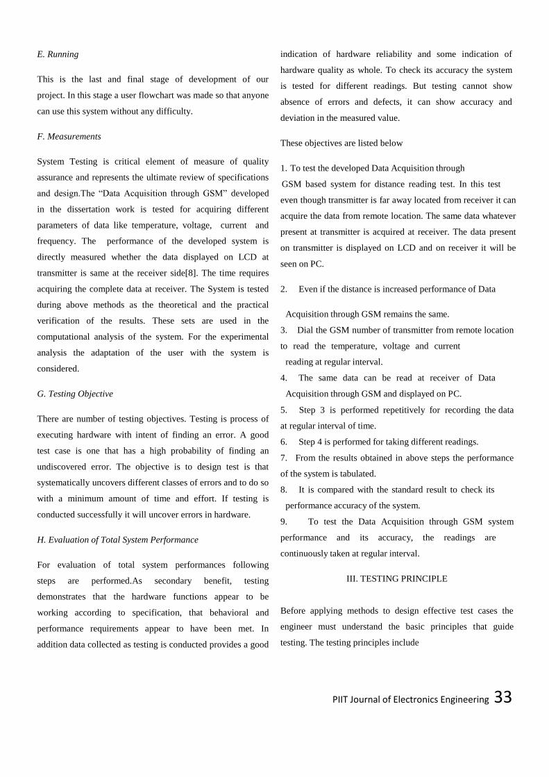
PIIT Journal of Electronics Engineering 33
E. Running
This is the last and final stage of development of our
project. In this stage a user flowchart was made so that anyone
can use this system without any difficulty.
F. Measurements
System Testing is critical element of measure of quality
assurance and represents the ultimate review of specifications
and design.The ―Data Acquisition through GSM‖ developed
in the dissertation work is tested for acquiring different
parameters of data like temperature, voltage, current and
frequency. The performance of the developed system is
directly measured whether the data displayed on LCD at
transmitter is same at the receiver side[8]. The time requires
acquiring the complete data at receiver. The System is tested
during above methods as the theoretical and the practical
verification of the results. These sets are used in the
computational analysis of the system. For the experimental
analysis the adaptation of the user with the system is
considered.
G. Testing Objective
There are number of testing objectives. Testing is process of
executing hardware with intent of finding an error. A good
test case is one that has a high probability of finding an
undiscovered error. The objective is to design test is that
systematically uncovers different classes of errors and to do so
with a minimum amount of time and effort. If testing is
conducted successfully it will uncover errors in hardware.
H. Evaluation of Total System Performance
For evaluation of total system performances following
steps are performed.As secondary benefit, testing
demonstrates that the hardware functions appear to be
working according to specification, that behavioral and
performance requirements appear to have been met. In
addition data collected as testing is conducted provides a good
indication of hardware reliability and some indication of
hardware quality as whole. To check its accuracy the system
is tested for different readings. But testing cannot show
absence of errors and defects, it can show accuracy and
deviation in the measured value.
These objectives are listed below
1. To test the developed Data Acquisition through
GSM based system for distance reading test. In this test
even though transmitter is far away located from receiver it can
acquire the data from remote location. The same data whatever
present at transmitter is acquired at receiver. The data present
on transmitter is displayed on LCD and on receiver it will be
seen on PC.
2. Even if the distance is increased performance of Data
Acquisition through GSM remains the same.
3. Dial the GSM number of transmitter from remote location
to read the temperature, voltage and current
reading at regular interval.
4. The same data can be read at receiver of Data
Acquisition through GSM and displayed on PC.
5. Step 3 is performed repetitively for recording the data
at regular interval of time.
6. Step 4 is performed for taking different readings.
7. From the results obtained in above steps the performance
of the system is tabulated.
8. It is compared with the standard result to check its
performance accuracy of the system.
9. To test the Data Acquisition through GSM system
performance and its accuracy, the readings are
continuously taken at regular interval.
III. TESTING PRINCIPLE
Before applying methods to design effective test cases the
engineer must understand the basic principles that guide
testing. The testing principles include
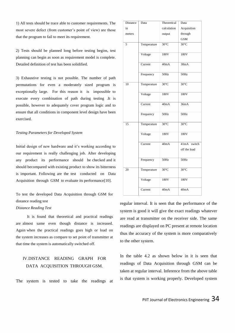
PIIT Journal of Electronics Engineering 34
Distance
in
meters
Data Theoretical
calculation
output
Data
Acquisition
through
GSM 5 Temperature 30°C 30°C
Voltage 180V 180V
Current 40mA 38mA
Frequency 50Hz 50Hz
10 Temperature 30°C 30°C
Voltage 180V 180V
Current 40mA 36mA
Frequency 50Hz 50Hz
15 Temperature 30°C 30°C
Voltage 180V 180V
Current 40mA 41mA switch
off the load
Frequency 50Hz 50Hz
20 Temperature 30°C 30°C
Voltage 180V 180V
Current 40mA 40mA
1) All tests should be trace able to customer requirements. The
most severe defect (from customer‘s point of view) are those
that the program to fail to meet its requirement.
2) Tests should be planned long before testing begins, test
planning can begin as soon as requirement model is complete.
Detailed definition of test has been solidified.
3) Exhaustive testing is not possible. The number of path
permutations for even a moderately sized program is
exceptionally large. For this reason it is impossible to
execute every combination of path during testing .It is
possible, however to adequately cover program logic and to
ensure that all conditions in component level design have been
exercised.
Testing Parameters for Developed System
Initial design of new hardware and it‘s working according to
our requirement is really challenging job. After developing
any product its performance should be checked and it
should becompared with existing product to show its bitterness
is important. Following are the test conducted on Data
Acquisition through GSM to evaluate its performance[10].
To test the developed Data Acquisition through GSM for
distance reading test
Distance Reading Test
It is found that theoretical and practical readings
are almost same even though distance is increased.
Again when the practical readings goes high or load on
the system increases as compare to set point of transmitter at
that time the system is automatically switched off.
IV.DISTANCE READING GRAPH FOR
DATA ACQUISITION THROUGH GSM.
The system is tested to take the readings at
regular interval. It is seen that the performance of the
system is good it will give the exact readings whatever
are read at transmitter on the receiver side. The same
readings are displayed on PC present at remote location
thus the accuracy of the system is more comparatively
to the other system.
In the table 4.2 as shown below in it is seen that
readings of Data Acquisition through GSM can be
taken at regular interval. Inference from the above table
is that system is working properly. Developed system
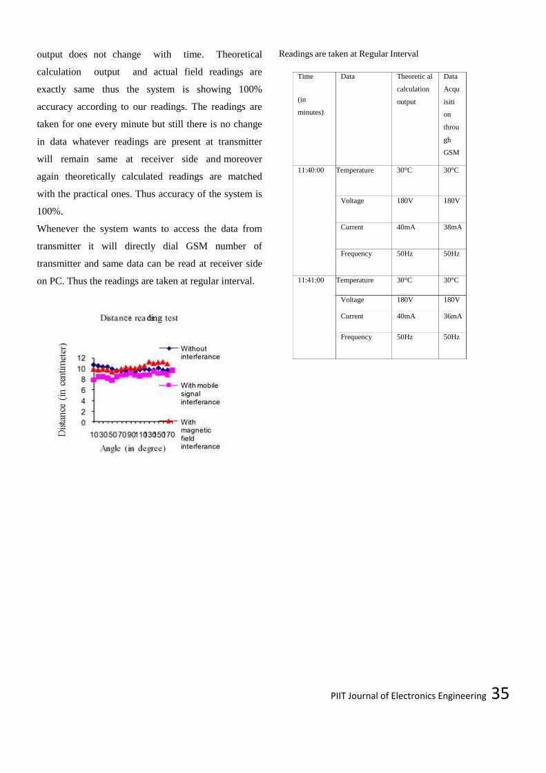
PIIT Journal of Electronics Engineering 35
Time
(in
minutes)
Data Theoretic al
calculation
output
Data
Acqu
isiti
on
throu
gh
GSM
11:40:00 Temperature 30°C 30°C
Voltage 180V 180V
Current 40mA 38mA
Frequency 50Hz 50Hz
11:41:00 Temperature 30°C 30°C
Voltage 180V 180V
Current 40mA 36mA
Frequency 50Hz 50Hz
output does not change with time. Theoretical
calculation output and actual field readings are
exactly same thus the system is showing 100%
accuracy according to our readings. The readings are
taken for one every minute but still there is no change
in data whatever readings are present at transmitter
will remain same at receiver side and moreover
again theoretically calculated readings are matched
with the practical ones. Thus accuracy of the system is
100%.
Whenever the system wants to access the data from
transmitter it will directly dial GSM number of
transmitter and same data can be read at receiver side
on PC. Thus the readings are taken at regular interval.
Readings are taken at Regular Interval

PIIT Journal of Electronics Engineering 36
11:50:00 Temperature 30°C 30°C
Voltage 180V 180V
Current 40mA 41mA
switch
off
the load
Frequency 50Hz 50Hz
11:51:00 Temperature 30°C 30°C
Voltage 180V 180V
Current 40mA 39mA
Frequency 50Hz 50Hz
11:52:00 Temperature 30°C 30°C
Voltage 180V 180V
Current 40mA 39mA
Frequency 50Hz 50Hz
11:53:00 Current 40mA
41mA
Switch off the load
Frequency 50Hz 50Hz
Analytical Analysis
Designed Data Acquisition system is compared using two-
method analytical and graphical method. In analytical method
%error is calculated using following formula.
% Error =
x100
Accuracy offers to degree of closeness or conformity to true
value of quantity under measurement. Accuracy of system is
calculated by following formula.
% Accuracy = 100 - %Error.
Comparison between Analytical and Experimental Analysis
Theoretical results of Data Acquisition through GSM are
compared with the practical value of Data Acquisition through
GSM. Graphical representation shows the comparison results of
Data Acquisition through GSM practical and theoretical results.
As curve for system and theoretical reading is overlapped it will
switch off the load. From the comparison it is clear that the
proposed system and calculated results are almost the same.
The results obtained in the above analysis analytical and
experimental for the data acquisition through GSM are tabulated
here.
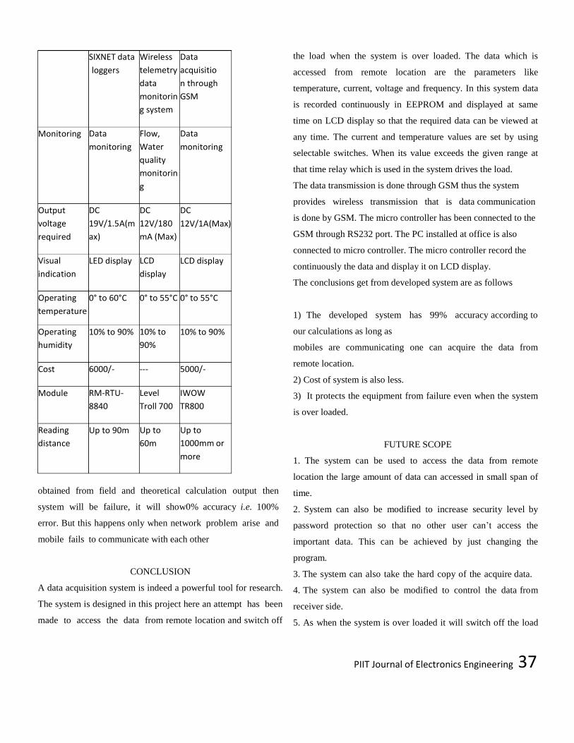
PIIT Journal of Electronics Engineering 37
SIXNET data
loggers
Wireless
telemetry
data
monitorin
g system
Data
acquisitio
n through
GSM
Monitoring Data
monitoring
Flow,
Water
quality
monitorin
g
Data
monitoring
Output
voltage
required
DC
19V/1.5A(m
ax)
DC
12V/180
mA (Max)
DC
12V/1A(Max)
Visual
indication
LED display LCD
display
LCD display
Operating
temperature
0° to 60°C 0° to 55°C 0° to 55°C
Operating
humidity
10% to 90% 10% to
90%
10% to 90%
Cost 6000/- --- 5000/-
Module RM-RTU-
8840
Level
Troll 700
IWOW
TR800
Reading
distance
Up to 90m Up to
60m
Up to
1000mm or
more
obtained from field and theoretical calculation output then
system will be failure, it will show0% accuracy i.e. 100%
error. But this happens only when network problem arise and
mobile fails to communicate with each other
CONCLUSION
A data acquisition system is indeed a powerful tool for research.
The system is designed in this project here an attempt has been
made to access the data from remote location and switch off
the load when the system is over loaded. The data which is
accessed from remote location are the parameters like
temperature, current, voltage and frequency. In this system data
is recorded continuously in EEPROM and displayed at same
time on LCD display so that the required data can be viewed at
any time. The current and temperature values are set by using
selectable switches. When its value exceeds the given range at
that time relay which is used in the system drives the load.
The data transmission is done through GSM thus the system
provides wireless transmission that is data communication
is done by GSM. The micro controller has been connected to the
GSM through RS232 port. The PC installed at office is also
connected to micro controller. The micro controller record the
continuously the data and display it on LCD display.
The conclusions get from developed system are as follows
1) The developed system has 99% accuracy according to
our calculations as long as
mobiles are communicating one can acquire the data from
remote location.
2) Cost of system is also less.
3) It protects the equipment from failure even when the system
is over loaded.
FUTURE SCOPE
1. The system can be used to access the data from remote
location the large amount of data can accessed in small span of
time.
2. System can also be modified to increase security level by
password protection so that no other user can‘t access the
important data. This can be achieved by just changing the
program.
3. The system can also take the hard copy of the acquire data.
4. The system can also be modified to control the data from
receiver side.
5. As when the system is over loaded it will switch off the load
PIIT Journal of Electronics Engineering 38
thus it protect the equipment from failure and therefore the
existing system can also be modified as UPS.
REFERENCES
1. John Park, Steve Mackay ―Practical data acquisition for
instrumentation‖ 1994, IEEE
Transactions on Wireless data communication, Vol.
12, No.8, 1990, pp. 787-808.
2. Omega Engineering Inc., The Data Acquisition
Systems Handbook. Stamford, CT The Curtis Publishing
Company, 2000.
3. Yuwen Zhai. The monitoring system of wireless data
transmission. International journal of wireless information
networks.1998, 5 (3). 187-202.
4. hester L Nachtigal ― Instrumentation and control‖
IEEE Transactions on Data Acquisition System, Vol.
18, No.10, October 1996, pp.1039-1045.
5. enneth.J.Ayala, ―89c51 architecture and programming
‖ Delinar Publisher, second edition.
6. Youbok Lee,‖ GSM Design‖, Microchip Technology
Inc.1998 Microchip Technology Inc.IEEE Transactions on
Data Acquisition System Intelligence, Vol. 18, No.10, October
1996, pp.1039-1045.
7. M.A.Mazidi and J.G.Mazidi, ―The 8051 microcontroller
and embedded systems‖ Pearson Education Publisher,
Thirteenth Indian Reprint.
8. L. Rabiner and B.H. Juang, ―Fundamental of Data
Acquisition through GSM‖, First Edition, Pearson
Education India, 1993, pp 257-261.
9.http://www.dataacquisitioncenter.com/wiki/accuracy/s
eries/2,accessdate:July20,2008.
10. http://www.chipsilicon.com/articles/series/1, access date:
May 15, 2008.
11.http://en.wikipedia.orgwiki/Data Acquisition, access date: July 17,
2008.

PIIT Journal of Electronics Engineering 39
Power Optimization for Turbo Coded CDMA
Prof. Seema P Mishra Asst. Professor.(ETRX Department)
Pillai Institute Of Information technology , [email protected]
Abstract-We utilize Extrinsic Information Transfer (EXIT)
charts to optimize the power allocation in a multiuser
CDMA system. We investigate two methods to obtain
the optimal power levels: the first minimizes the total
power; the second minimizes the area between the transfer
curves of the interference canceller (IC) or turbo decoder.
We show through simulation that the optimized power
levels allow for successful decoding of heavily loaded
systems. The optimal decoding schedule is derived
dynamically using the power optimized EXIT chart and
a Viterbi search algorithm. Dynamic scheduling is
shown to be a more flexible approach which results in a
more stable QoS for a typical system configuration than
one-shot scheduling, and large complexity savings over a
receiver without scheduling. We propose dynamic decoding
schedule optimization to fix the problem, that is, on each
iteration of the receiver derive the optimal schedule to
achieve a target bit error rate using a minimum
number of turbo decoder iterations.
I. INTRODUCTION
The adventage of the turbo decoding algorithm for
parallel concatenated codes, a decade ago ranks among the
most significant breakthroughs in modern communications in
the past half century: a coding and decoding procedure of
reasonable computational complexity was finally at hand
offering performance approaching the previously elusive
Shannon limit, which predicts reliable communications for all
channel capacity rates slightly in excess of the source entropy
rate. The practical success of the iterative turbo
decoding algorithm has inspired its adaptation to other code
classes, notably serially concatenated codes, and has
rekindled interest in low-density parity-check codes, which
give the definitive historical precedent in iterative decoding.
The serial concatenated configuration holds particular interest
for communication systems, since the ―inner encoder‖ of such
a configuration can be given more general interpretations, such
as a ―parasitic‖ encoder induced by a convolutional channel or
by the spreading codes used in CDMA. The corresponding
iterative decoding algorithm can then be extended into new
arenas, giving rise to turbo equalization or turbo
CDMA, among doubtless other possibilities. Such
applications demonstrate thepower of iterative techniques
which aim to jointly optimize receiver components, compared
to the traditional approach of adapting such components
independently of one another. Algorithms are often
developed and tested in floating- point environments on
GPPs in order to show the achievable optimal
performance. Besides shortest development time, there
are no requirements on, for example, processing speed or
power consumption, and hence this platform is the best choice
for the job. However, speed or power constraints might require
an implementation in more or less specialized hardware. This
transition usually causes many degradations, for example,
reduced dynamic range caused by fixed-point arithmetic,
which on the other hand provides tremendous reduction in
implementation complexity.
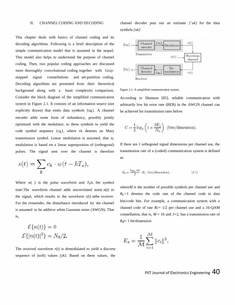
PIIT Journal of Electronics Engineering 40
II. CHANNEL CODING AND DECODING
This chapter deals with basics of channel coding and its
decoding algorithms. Following is a brief description of the
simple communication model that is assumed in the sequel.
This model also helps to understand the purpose of channel
coding. Then, two popular coding approaches are discussed
more thoroughly: convolutional coding together with Gray-
mapped signal constellations and set-partition coding.
Decoding algorithms are presented from their theoretical
background along with a basic complexity comparison.
Consider the block diagram of the simplified communication
system in Figure 2.1. It consists of an information source (not
explicitly drawn) that emits data symbols uk. A channel
encoder adds some form of redundancy, possibly jointly
optimized with the modulator, to these symbols to yield the
code symbol sequence ck, where ck denotes an Mary
transmission symbol. Linear modulation is assumed, that is,
modulation is based on a linear superposition of (orthogonal)
pulses. The signal sent over the channel is therefore
Where w( ) is the pulse waveform and Tsis the symbol
time.The waveform channel adds uncorrelated noise n(t) to
the signal, which results in the waveform r(t) atthe receiver.
For the remainder, the disturbance introduced by the channel
is assumed to be additive white Gaussian noise (AWGN). That
is,
The received waveform r(t) is demodulated to yield a discrete
sequence of (soft) values yk. Based on these values, the
channel decoder puts out an estimate ˆuk for the data
symbols uk
Figure 2.1: A simplified communication system.
According to Shannon [85], reliable communication with
arbitrarily low bit error rate (BER) in the AWGN channel can
be achieved for transmission rates below
If there are J orthogonal signal dimensions per channel use, the
transmission rate of a (coded) communication system is defined
as
whereM is the number of possible symbols per channel use and
Rc<1 denotes the code rate of the channel code in data
bits/code bits. For example, a communication system with a
channel code of rate Rc= 1/2 per channel use and a 16-QAM
constellation, that is, M = 16 and J=2, has a transmission rate of
Rd= 1 bit/dimension
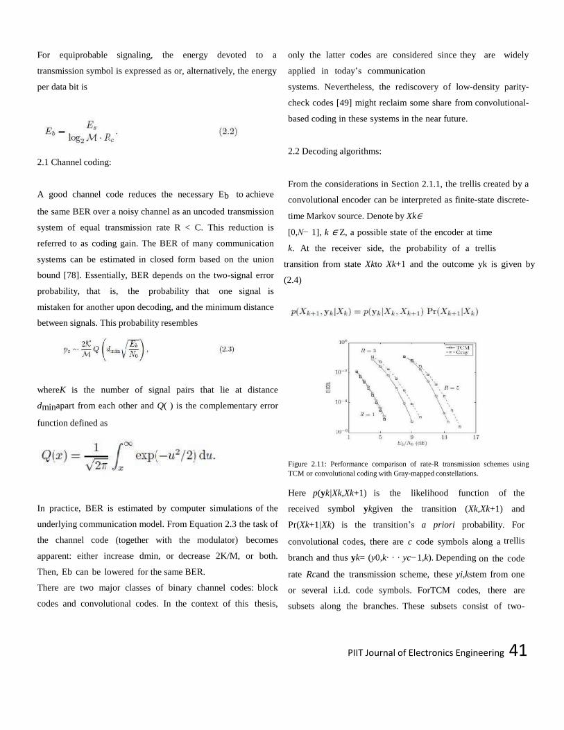
PIIT Journal of Electronics Engineering 41
For equiprobable signaling, the energy devoted to a
transmission symbol is expressed as or, alternatively, the energy
per data bit is
2.1 Channel coding:
A good channel code reduces the necessary Eb to achieve
the same BER over a noisy channel as an uncoded transmission
system of equal transmission rate R < C. This reduction is
referred to as coding gain. The BER of many communication
systems can be estimated in closed form based on the union
bound [78]. Essentially, BER depends on the two-signal error
probability, that is, the probability that one signal is
mistaken for another upon decoding, and the minimum distance
between signals. This probability resembles
whereK is the number of signal pairs that lie at distance
dminapart from each other and Q( ) is the complementary error
function defined as
In practice, BER is estimated by computer simulations of the
underlying communication model. From Equation 2.3 the task of
the channel code (together with the modulator) becomes
apparent: either increase dmin, or decrease 2K/M, or both.
Then, Eb can be lowered for the same BER.
There are two major classes of binary channel codes: block
codes and convolutional codes. In the context of this thesis,
only the latter codes are considered since they are widely
applied in today‘s communication
systems. Nevertheless, the rediscovery of low-density parity-
check codes [49] might reclaim some share from convolutional-
based coding in these systems in the near future.
2.2 Decoding algorithms:
From the considerations in Section 2.1.1, the trellis created by a
convolutional encoder can be interpreted as finite-state discrete-
time Markov source. Denote by Xk∈
[0,N− 1], k ∈ Z, a possible state of the encoder at time
k. At the receiver side, the probability of a trellis
transition from state Xkto Xk+1 and the outcome yk is given by
(2.4)
Figure 2.11: Performance comparison of rate-R transmission schemes using
TCM or convolutional coding with Gray-mapped constellations.
Here p(yk|Xk,Xk+1) is the likelihood function of the
received symbol ykgiven the transition (Xk,Xk+1) and
Pr(Xk+1|Xk) is the transition‘s a priori probability. For
convolutional codes, there are c code symbols along a trellis
branch and thus yk= (y0,k· · · yc−1,k). Depending on the code
rate Rcand the transmission scheme, these yi,kstem from one
or several i.i.d. code symbols. ForTCM codes, there are
subsets along the branches. These subsets consist of two-
PIIT Journal of Electronics Engineering 42
dimensional signals and ykis a two-dimensional signal. When
a demodulated noisy value yk is received from an AWGN
channel with variance σ2 = N0/2, the likelihood function
becomes
One can take the logarithm of Equation 2.8 and scale with −N0
to yield the branch metric (BM)
(2.6)
And
(2.7)
respectively. Clearly, ML and MAP decoders would estimate
the same symbol sequence if all symbols were equally likely,
that is, the a priori probability is equal for all branches. Then,
the second term in Equation 2.11 is the same for all branches
(Xi,Xi+1), and can thus be removed in calculating the branch
metrics. If there is a priori information about the transition,
though, the decoding might give different results for ML and
MAP. In any case, ML minimizes the sequence error
probability, whereas MAP can be set up so as to minimize the
bit error probability [8].
III. TURBO CODES
In information theory, turbo codes (originally in French Turbo
codes) are a class of high-performance forward error correction
(FEC) codes developed in 1993, which were the first practical
codes to closely approach the channel capacity, a theoretical
maximum for the code rate at which reliable communication
is still possible given a specific noise level. Turbo codes are
finding use in (deep space) satellitecommunications and other
applications where designers seek to achieve reliable
information transfer over bandwidth- or latency- constrained
communication links in the presence of data-corrupting
noise. Turbo codes are nowadays competing with LDPC codes,
which provide similar performance.
Soft decision approach:
The decoder front-end produces an integer for each bit in the
data stream. This integer is a measure of how
likely it is that the bit is a 0 or 1 and is also called soft bit.
The integer could be drawn from the range [-127,
127], where:
-127 means "certainly 0"
-100 means "very likely 0"
0 means "it could be either 0 or 1"
100 means "very likely 1"
127 means "certainly 1"
etc.
This introduces a probabilistic aspect to the data-stream from
the front end, but it conveys more information about each bit
than just 0 or 1
IV. SYSTEM DESCRIPTION
A.Existing system:
The turbo decoding algorithm for error-correction codes is known
not to converge, in general, to a maximum likelihood solution,
although in practice it is usually observed to give comparable
performance. The quest to understand the convergence behavior
has spawned numerous inroads, including extrinsic information
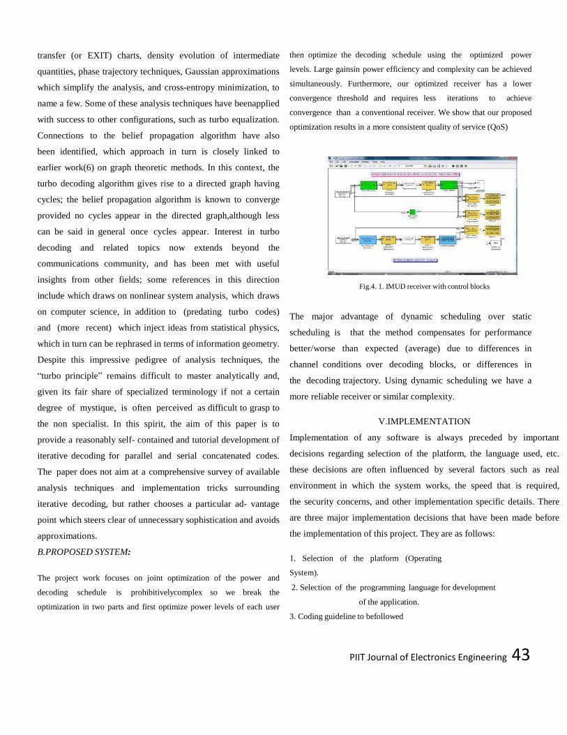
PIIT Journal of Electronics Engineering 43
transfer (or EXIT) charts, density evolution of intermediate
quantities, phase trajectory techniques, Gaussian approximations
which simplify the analysis, and cross-entropy minimization, to
name a few. Some of these analysis techniques have beenapplied
with success to other configurations, such as turbo equalization.
Connections to the belief propagation algorithm have also
been identified, which approach in turn is closely linked to
earlier work(6) on graph theoretic methods. In this context, the
turbo decoding algorithm gives rise to a directed graph having
cycles; the belief propagation algorithm is known to converge
provided no cycles appear in the directed graph,although less
can be said in general once cycles appear. Interest in turbo
decoding and related topics now extends beyond the
communications community, and has been met with useful
insights from other fields; some references in this direction
include which draws on nonlinear system analysis, which draws
on computer science, in addition to (predating turbo codes)
and (more recent) which inject ideas from statistical physics,
which in turn can be rephrased in terms of information geometry.
Despite this impressive pedigree of analysis techniques, the
―turbo principle‖ remains difficult to master analytically and,
given its fair share of specialized terminology if not a certain
degree of mystique, is often perceived as difficult to grasp to
the non specialist. In this spirit, the aim of this paper is to
provide a reasonably self- contained and tutorial development of
iterative decoding for parallel and serial concatenated codes.
The paper does not aim at a comprehensive survey of available
analysis techniques and implementation tricks surrounding
iterative decoding, but rather chooses a particular ad- vantage
point which steers clear of unnecessary sophistication and avoids
approximations.
B.PROPOSED SYSTEM:
The project work focuses on joint optimization of the power and
decoding schedule is prohibitivelycomplex so we break the
optimization in two parts and first optimize power levels of each user
then optimize the decoding schedule using the optimized power
levels. Large gainsin power efficiency and complexity can be achieved
simultaneously. Furthermore, our optimized receiver has a lower
convergence threshold and requires less iterations to achieve
convergence than a conventional receiver. We show that our proposed
optimization results in a more consistent quality of service (QoS)
Fig.4. 1. IMUD receiver with control blocks
The major advantage of dynamic scheduling over static
scheduling is that the method compensates for performance
better/worse than expected (average) due to differences in
channel conditions over decoding blocks, or differences in
the decoding trajectory. Using dynamic scheduling we have a
more reliable receiver or similar complexity.
V.IMPLEMENTATION
Implementation of any software is always preceded by important
decisions regarding selection of the platform, the language used, etc.
these decisions are often influenced by several factors such as real
environment in which the system works, the speed that is required,
the security concerns, and other implementation specific details. There
are three major implementation decisions that have been made before
the implementation of this project. They are as follows:
1. Selection of the platform (Operating
System).
2. Selection of the programming language for development
of the application.
3. Coding guideline to befollowed
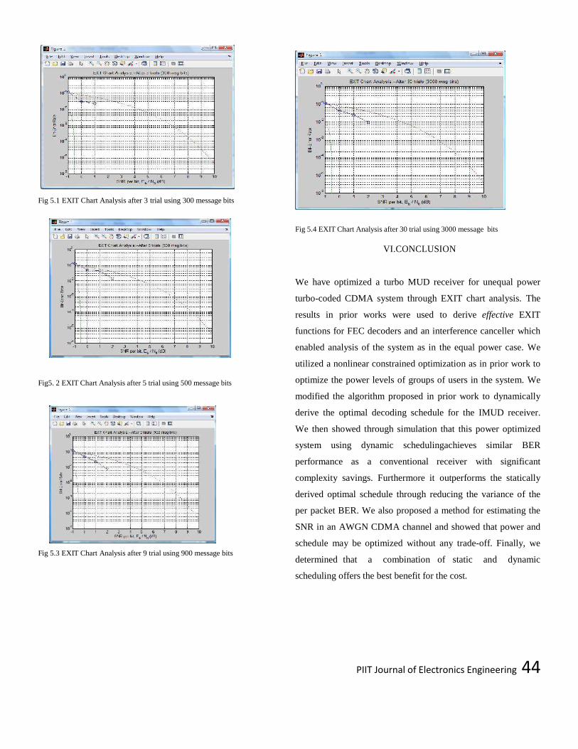
PIIT Journal of Electronics Engineering 44
Fig 5.1 EXIT Chart Analysis after 3 trial using 300 message bits
Fig5. 2 EXIT Chart Analysis after 5 trial using 500 message bits
Fig 5.3 EXIT Chart Analysis after 9 trial using 900 message bits
Fig 5.4 EXIT Chart Analysis after 30 trial using 3000 message bits
VI.CONCLUSION
We have optimized a turbo MUD receiver for unequal power
turbo-coded CDMA system through EXIT chart analysis. The
results in prior works were used to derive effective EXIT
functions for FEC decoders and an interference canceller which
enabled analysis of the system as in the equal power case. We
utilized a nonlinear constrained optimization as in prior work to
optimize the power levels of groups of users in the system. We
modified the algorithm proposed in prior work to dynamically
derive the optimal decoding schedule for the IMUD receiver.
We then showed through simulation that this power optimized
system using dynamic schedulingachieves similar BER
performance as a conventional receiver with significant
complexity savings. Furthermore it outperforms the statically
derived optimal schedule through reducing the variance of the
per packet BER. We also proposed a method for estimating the
SNR in an AWGN CDMA channel and showed that power and
schedule may be optimized without any trade-off. Finally, we
determined that a combination of static and dynamic
scheduling offers the best benefit for the cost.
PIIT Journal of Electronics Engineering 45
REFERENCES
[1] G. Caire, R. M¨uller, and T. Tanaka, ―Iterative multiuser joint
decoding: Optimal power allocation and low-complexity
implementation,‖ IEEE Trans. Inform. Theory, vol. 50, no. 9, pp.
1950–1973, Sept. 2004.
[2] C. Schlegel and Z. Shi, ―Optimal power allocation and code
selection in iterative detection of random CDMA,‖ in Proc. Zurich
Seminar on Communications, Zurich, Switzerland, Feb. 2004, pp. 98–
101.
[3] R. M¨uller and G. Caire, ―The optimal received power
distribution for IC-based iterative multiuser joint decoders,‖ in Proc.
Allerton Conf. on Commun., Control and Computing, Monticello,
USA, Oct. 2001.
[4] S. ten Brink, ―Convergence behavior of iteratively decoded parallel
concatenated codes,‖ IEEE Trans. Commun., vol. 49, no. 10, pp.
1727–1737, Oct. 2001.
[5] F. Br¨annstr¨om, L. K. Rasmussen, and A. J. Grant, ―Convergence
analysis and optimal scheduling for multiple concatenated codes,‖
IEEE Trans. Inform. Theory, vol. 51, pp. 3354–3364, Sept. 2005.
[6] D. P. Shepherd, F. Br¨annstr¨om, and M. C. Reed,
―Minimising complexity in iterative multiuser detection using dynamic
decoding schedules,‖ in Proc. IEEE Int. Workshop on Sig. Proc.
Advanced in Wireless Communications, Cannes, France, 2006, pp. 1–
5.
[7] K. Li and X. Wang, ―EXIT chart analysis of turbo multiuser
detection,‖ IEEE Trans. Wireless Commun., vol. 4, no. 1, pp. 300–
311, Jan. 2005.
[8] J. W. Lee and R. E. Blahut, ―Convergence analysis and BER
performance of finite-length turbo codes,‖ IEEE Trans. Commun., vol.
55, no. 5, pp. 1033–1043, May 2007.
[9] D. P. Shepherd, F. Schreckenbach, and M. C. Reed, ―Optimization
of unequal power coded multiuser DS- CDMA using extrinsic
information transfer charts,‖ in Proc. Conf. Info. Sciences and
Systems, Princeton, USA, Mar. 2006, pp. 1435–1439.
[10] D. Shepherd, F. Br¨annstr¨om, and M. Reed, ―Dynamic
scheduling for a turbo CDMA receiver using EXIT charts,‖ in
Proc. Aust. Commun. Theory Workshop, Adelaide, Australia, Feb.
2007, pp. 34–38.
[11] P. D. Alexander, A. J. Grant, and M. C. Reed, ―Performance
analysis of an iterative decoder for code- division multiple-access,‖
European Trans. Telecom., vol. 9, no. 5, pp. 419–426, Sept./Oct.
1998.
[12] ―3GPP TS 25.104 V5.9.0; 3rd generation partnership
project; technical specification group radio access network;base station
(BS) radio transmission and
reception (FDD) (release 5),‖ Sept. 2004.
[13] D. P. Shepherd, Z. Shi, M. Anderson, and M. C. Reed, ―EXIT
chart analysis of an iterative receiver with channel estimation,‖ in
Proc. IEEE Global
Telecommunications Conf., Washington D.C., USA, Nov. 2007, pp.
4010–4014.
[14] Z. Shi and C. Schlegel, ―Performance analysis of iterative
detection for unequal power coded CDMA systems,‖ in Proc.
IEEE Global Telecommunications
Conf., vol. 3, Dec. 2003, pp. 1537–1542.
[15] D. P. Shepherd, F. Br¨annstr¨om, and M. C. Reed, ―Fidelity
charts and stopping/termination criteria for iterative multiuser
detection,‖ in Proc. 4th Int. Symp. On Turbo Codes and Related
Topics, Munich, Germany, 2006.
[16] F. Br¨annstr¨om and L. K. Rasmussen, ―Non-data- aided
parameter estimation in an additive white Gaussian noise channel,‖ in
Proc. IEEE Int. Symp.on Info. Theory, Adelaide, Australia, 2005,
pp. 1446–1450.
[17] F. Br¨annstr¨om, ―Convergence analysis and design of multiple
concatenated codes,‖ Ph.D. dissertation, Chalmers University of
Technology, G¨oteborg Sweden, 2004.
[18] M. Tuchler and J. Hagenauer, ―EXIT charts of irregular
codes,‖ in Proc. Conf. Info. Sciences and
Systems, Princeton, USA Mar. 2002.
[19] F. Schreckenbach and G. Bauch, ―Bit-interleaved coded irregular
modulation,‖ European Trans. Telecommun., vol. 17, pp. 269–282,
Mar. 2006.
[20] T. Coleman and Y. Li, ―An interior, trust region approach for
nonlinear minimization subject to bounds,‖ SIAM J. Optimization, vol.
6, pp. 418–445, 1996.
[21] ——, ―On the convergence of reflective newton methods for
large-scale nonlinear minimization subject bounds,‖ Mathematical
Programming, vol. 67, no. 2, pp. 189–224, 1996.
[22] V. Franz and J. B. Anderson, ―Concatenated
decoding with a reduced search BCJR algorithm,‖ IEEE J. Select.
Areas Commun., vol. 16, no. 2, pp. 186–195, Feb. 1998.
[23] U. Dasgupta and K. R. Narayanan, ―Parallel decoding of
turbo codes using soft output T-algorithms,‖ IEEE Commun. Lett.,
vol. 5, no. 8, pp. 352–354, Aug. 2001
PIIT Journal of Electronics Engineering 46
INTERACTIVE VOICE RESPONSE SYSTEM FOR
EDUCATIONAL INSTITUTION
Prof.Seema P Mishra
Address for Correspondence
Asst.Prof. (ETRX Dept.)
PIIT
New Panvel, Mumbai
Prof.Apeksha S.Chavan,
Address for Correspondence
Asst.Prof.(ETRX Dept.)
PIIT
New Panvel, Mumbai
Prof.Swapnil S. Gourkar
Address for Correspondence
Asst.Prof.(ETRX Dept.)
PIIT
New Panvel, Mumbai
Abstract-The Interactive Voice Response(IVR) system serves as a
bridge between people and computer databases by connecting the
telephone network with database. The telephone user can acces the
information from anywhere at any time simply by dialing a
specified number and following an on-line instruction when a
connection has been established. The IVR system uses prerecorded
or computer generated voice responses to provide information in
response to an input from a telephone column.The input may be
given by means of touch-tone or Dual Tone Multi-
Frequency(DTMF)signal which is generated when a caller presses a
key of his/a telephone set,and the sequence of messages to be played
is determined dynamically according to an internal menu
structure(maintained within the IVR application program) and the
user input. The IVR system which will be designed will provide an
ideal platform for the operation of start-ups and existing small
concerns. It will be a highly economical and efficient way to replace
the Dialogic card which is very costly and requires a high
maintenance and regular up gradation. The IVR system which will
be designed will consist of simple components like microcontroller
and some basic application chips interfaced to a PC which will have
a small software running in the backend while the other jobs are
performed on the front end.
I.INTRODUCTION
Interactive Voice Response systems can play a significant
role in providing efficient customer service. Properly
implemented, they can increase customer satisfaction, lower
costs and offer new services. The return on investment (ROI) on
these systems is also quite amazing, making them the most
popular Computer Telephony systems in the world. Compare
them to a call center. The price for the extra ―human touch‖
translates into a huge running cost in the form of Agents,
Supervisors, infrastructure maintenance, training, call center
performance & discipline reviews, etc. World over, the first
systems that any company deploys with a view towards
enhancing customer satisfaction are IVR‘s. Call centers come
much later. IVR‘s can provide information to callers in one of
two ways:
Pre-recorded information.
Common examples are audio movie snippet previews
(e.g. at PVR). Though it is possible to build these IVR‘s
through live information from databases (using text-to-speech
engines), one doesn‘t get the voice variations, which are so
important for the moviegoer. Other examples are around
procedural (or ―how to‖) information dissemination like
Income tax filing procedures, bank account opening or credit
card application procedures, etc.
Live information from databases.
These IVR‘s get information from databases, convert to
voice, and speaks it back to the caller. Practically all industry

PIIT Journal of Electronics Engineering 47
segments are potential users for this, and examples include
Phone banking (where you call in, dial in your account number
& TPIN and can hear your account balance on phone) Courier
packet trace (where you call in, dial the AWB number, and the
system tells you whether the packet has been delivered, if it is
in transit, etc).
Microcontroller Based IVRs For College Automation.
In telephony, interactive voice response, or IVR, is a
phone technology that allows a computer to detect voice and
touch tones using a normal phone call. The IVR system can
respond with pre-recorded or dynamically generated audio to
further direct callers on how to proceed. IVR systems can be
used to control almost any function where the interface can be
broken down into a series of simple menu choices. Once
constructed IVR systems generally scale well to handle large
call volumes.
Now-a-days every institution needs automation. As a
part of college automation, we have decided to do a project.
Voice Interactive System for College Automation. Our project
allows the user to know the student attendance and marks
quickly through the telephone line without the intention of the
college authority. In the hardware side embedded system has
been used. It will be very obliging to the parents to be
acquainted with their son/daughter recital in the college.
In the hardware side embedded system has been used.
A 20 pin microcontroller 89C2051 is used because of its
compatibility with our hardware. This microcontroller controls
the whole hardware. Telephone line is used for communication
purpose. Visual Basic has been used for software
programming. Presentation in the class and outcome of the
university are made reachable to students and parents on phone
by our project.
Interactive Voice Response (IVR) is a software
application that accepts a combination of voice telephone input
and touch-tone keypad selection and provides appropriate
responses in the form of voice, fax, callback, e-mail and
perhaps other media. IVR is usually part of a larger application
that includes database access.
An IVR application provides pre-recorded voice
responses for appropriate situations, keypad signal logic, and
access to relevant data, and potentially the ability to record
voice input for later handling. Using computer telephony
Integration (CTI), IVR applications can hand off a call to a
human being who can view data related to the caller at a
display. Interactive Voice Response (IVR) systems allow
callers to get access to information without human
intervention. Thus callers hear a pleasant and cheerful
voice 24-hours a day, 7 days a year without any attendant
human fatigue.
Since even the cost of the call is borne by the caller,
apart from the one-time installation cost, there is no running
expense for the company who deploys the IVR systems.
Another advantage to the company is that it would otherwise
be impossible to handle high loads of callers, both in terms of
time, and the cost of the large number of individuals that it
would require.
II. INTERACTIVE VOICE RESPONSE SYSTEM
FEATURES
1. Simple t o u s e Graphical System Design
Interface
2. Multiple t e l e p h o n e line support both on
Analog and Digital
3. Advanced call screening and call switching options
4. Can be integrated with any type of database.
Playback data retrieved from Database
5. Text to Speech
6. Call Transfer to other extensions, optionally announcing
the Caller ID, allowing the recipient to accept or
decline the call
7. Full logging of callers' details and all the selections

PIIT Journal of Electronics Engineering 48
made during the call
8. Multi-Language support (English /Hindi)
9. DNIS: (Dialed number identification service)
10. ANI: (Automatic Number Identification)
11. Common IVR applications include:
12. Schools, Colleges and Educational Institutions
13. Bank and stock account balances and transfers
14. Surveys and polls
15. Call center forwarding
16. Simple order entry transactions
17. Selective information lookup (movie schedules,
etc.)
18. Ticketing and Reservation
19. IT Enabled Services
20. Hotels, Airline & Train Ticket Enquiry & Booking
Centers
21. Entertainment Industry
22. Complaint Booking and Customer Support Centers
23. Banks, Finance and Credit Corporations
24. Tele-Marketing Industry –Outbound Calls
IVRS for an Educational Institution
An IVRS is an exemplary innovation in the area of
voice assisted browsing and data retrieval on telephone, data
that contains information of interest and has straight
relevance to the user. This application software allows full
resource sharing and integration with the existing database of :
Our Software solution for the complete computerization
of Educational Institutions, for e.g. in a) Visual Basics 6.0 &
(MS –Access 2003). The software first converts the data into a
voice format and then sends it on to the telephony network. The
voice response by the system is then heard by the caller, and as
discussed, shall cover the following informational requirements:
1. Fees Installment Paid/Due Status of the
Student.
2. Attendance status for any day, week, month or entire
year.
3. Marks scored in any test or exam.
4. Rank in any test or exam.
5. Percentage scored in exam.
6. Score, rank and percentage in any particular subject.
7. Homework for any day.
8. Remarks given by teachers.
9. Timetable.
10. Test schedule and test syllabus.
11. Dates of admission, pre-requisites for admission and
status of admission for any application.
12. Vacancies for faculty, if any.
13. Any important announcements for parents like dates
for parents-teachers meetings or any other messages.
14. Automatic Fee Reminders on student
telephone numbers.
15. Voice mail accounts for each and every student
(especially in case of a boarding school), to help
parents leave important messages for their wards.
Parents‘ Grievance Box, to make parents leave their
grievances about their child‘s performance, for any subject. The
recorded grievance is then automatically sent to the voice
mailbox of the teacher who takes that particular subject in the
class. The basic system can handle 4 incoming calls at one
point of time, 24 hours a day, 7 days a week and 365 days a
year.
The Hardware Requirement
• A Server computer
• Telephony cards that answer calls
• IVR software
Apart from this, there needs to be connection to the
database from where the Information will be picked up.
This is generally through an IP based network. Apart from
delivering information by voice, there are other methods,
as well that one should consider. They are fax, email &
PIIT Journal of Electronics Engineering 49
SMS. For instance, if the caller wanted an account
statement from his bank, voice is quite useless, Fax or
email are better options. The system can be integrated with
applications to send Emails, fax, SMS features. Thus
1. Relay: For switching between the ring detector
and the DTMF decoder.
2. Ring detector: To detect the presence of incoming calls.
3. DTMF decoder: To convert the DTMF tones
to 4 bit BCD codes.
4. Micro controller: To accept the BCD calls, process
them and transmit them serially to the PC.
5. Level Translator: To provide the interface between PC
and micro controller.
6. Personal Computer: To store the data base and to
carry out the text to speech conversion.
7. Audio Amplifier: To provide audio amplification to
standard output and to act as a buffer between the
telephone line and sound card.
III. SEQUENCE FOLLOWED IN THE IVRS
SERVICE
• Caller dials the IVRS service number.
• The computer waits for a specified number of
ringing tones at the end of which, the connection is
established.
• The connection is established by lifting the handset
of telephone base from ONHOOK condition.
• Now, a pre-recorded voice greets the caller
conforming that the number dialed corresponding to
the particular service.
• Next, the menu is presented to the caller again in
the voice form, giving him then various options to
choose from.
• If the information to be relayed back is
confidential, then the system may even ask the dialer,
to feed in a password number.
• The database is accordingly referenced and the
necessary information is obtained.
• Next, the same information is put across to the user in
voice.
• The caller generally given the option to :
a. Repeat whatever information was voiced to
him.
b. Repeat the choices.
c. Break the call by restarting ON-HOOK
condition.
CIRCUIT DIAGRAM of IVR System
Figure 1 Shows diagram of IVR System for college
automation system. Any telephone set will always be in any
of the conditions mentioned below:
ON-HOOK
It is the state whenever telephone handset is placed
on the cradle. During this state, the telephone line is open
circuit with the exchange and the voltage of
–48 V is available on each telephone line from the exchange.
OFF-HOOK
This is the state whenever telephone handset is
displaced from the cradle. During this state the voltage
level is between ± 5V to ± 12 V. The telephone OFF –
HOOK resistance is typically 600 Ω SIGNALING TONES
• Dial tone: This tone indicates that the exchange is
ready to accept dialed digits from the subscriber. The
subscriber should start dialing only after hearing the
dial tone. Otherwise, initial dialed pulse may be missed
by the exchange that may result in the call landing on
the wrong number. The dialed tone is 33 Hz or 50 Hz
or 400 Hz continuous tones.
• Ring tone: When the called party is obtained, the
exchange sense out the ringing current to the telephone
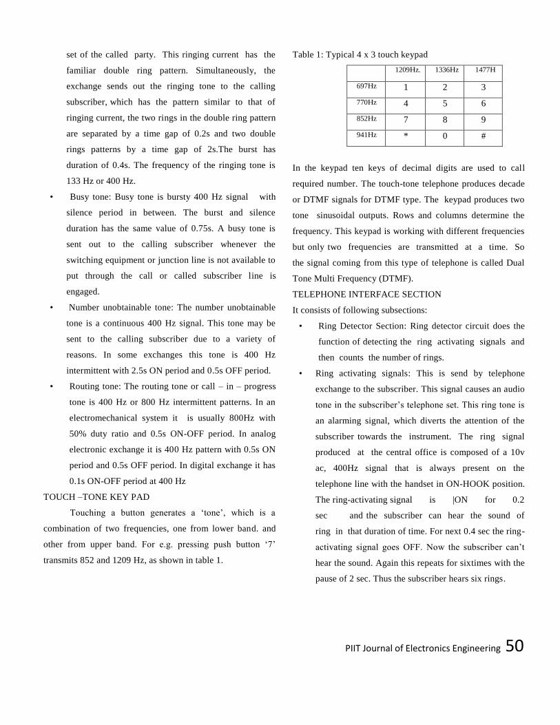
PIIT Journal of Electronics Engineering 50
set of the called party. This ringing current has the
familiar double ring pattern. Simultaneously, the
exchange sends out the ringing tone to the calling
subscriber, which has the pattern similar to that of
ringing current, the two rings in the double ring pattern
are separated by a time gap of 0.2s and two double
rings patterns by a time gap of 2s.The burst has
duration of 0.4s. The frequency of the ringing tone is
133 Hz or 400 Hz.
• Busy tone: Busy tone is bursty 400 Hz signal with
silence period in between. The burst and silence
duration has the same value of 0.75s. A busy tone is
sent out to the calling subscriber whenever the
switching equipment or junction line is not available to
put through the call or called subscriber line is
engaged.
• Number unobtainable tone: The number unobtainable
tone is a continuous 400 Hz signal. This tone may be
sent to the calling subscriber due to a variety of
reasons. In some exchanges this tone is 400 Hz
intermittent with 2.5s ON period and 0.5s OFF period.
• Routing tone: The routing tone or call – in – progress
tone is 400 Hz or 800 Hz intermittent patterns. In an
electromechanical system it is usually 800Hz with
50% duty ratio and 0.5s ON-OFF period. In analog
electronic exchange it is 400 Hz pattern with 0.5s ON
period and 0.5s OFF period. In digital exchange it has
0.1s ON-OFF period at 400 Hz
TOUCH –TONE KEY PAD
Touching a button generates a ‗tone‘, which is a
combination of two frequencies, one from lower band. and
other from upper band. For e.g. pressing push button ‗7‘
transmits 852 and 1209 Hz, as shown in table 1.
Table 1: Typical 4 x 3 touch keypad
1209Hz. 1336Hz 1477H
697Hz 1 2 3
770Hz 4 5 6
852Hz 7 8 9
941Hz * 0 #
In the keypad ten keys of decimal digits are used to call
required number. The touch-tone telephone produces decade
or DTMF signals for DTMF type. The keypad produces two
tone sinusoidal outputs. Rows and columns determine the
frequency. This keypad is working with different frequencies
but only two frequencies are transmitted at a time. So
the signal coming from this type of telephone is called Dual
Tone Multi Frequency (DTMF).
TELEPHONE INTERFACE SECTION
It consists of following subsections:
• Ring Detector Section: Ring detector circuit does the
function of detecting the ring activating signals and
then counts the number of rings.
• Ring activating signals: This is send by telephone
exchange to the subscriber. This signal causes an audio
tone in the subscriber‘s telephone set. This ring tone is
an alarming signal, which diverts the attention of the
subscriber towards the instrument. The ring signal
produced at the central office is composed of a 10v
ac, 400Hz signal that is always present on the
telephone line with the handset in ON-HOOK position.
The ring-activating signal is |ON for 0.2
sec and the subscriber can hear the sound of
ring in that duration of time. For next 0.4 sec the ring-
activating signal goes OFF. Now the subscriber can‘t
hear the sound. Again this repeats for sixtimes with the
pause of 2 sec. Thus the subscriber hears six rings.
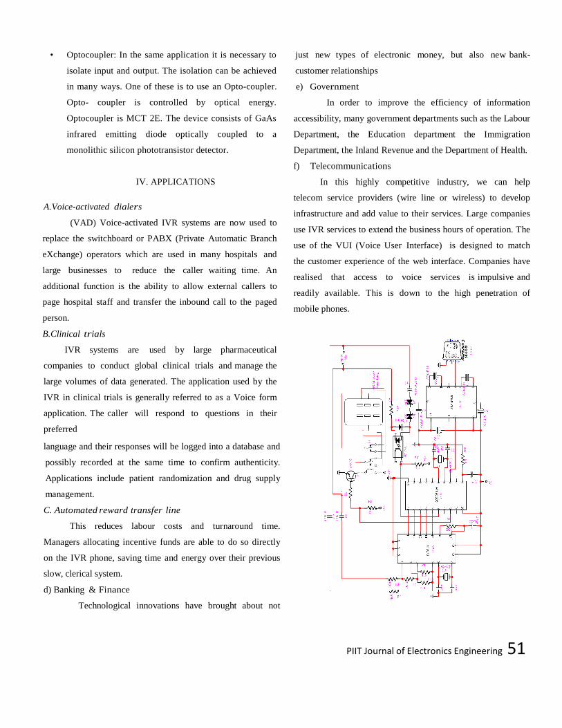
PIIT Journal of Electronics Engineering 51
• Optocoupler: In the same application it is necessary to
isolate input and output. The isolation can be achieved
in many ways. One of these is to use an Opto-coupler.
Opto- coupler is controlled by optical energy.
Optocoupler is MCT 2E. The device consists of GaAs
infrared emitting diode optically coupled to a
monolithic silicon phototransistor detector.
IV. APPLICATIONS
A.Voice-activated dialers
(VAD) Voice-activated IVR systems are now used to
replace the switchboard or PABX (Private Automatic Branch
eXchange) operators which are used in many hospitals and
large businesses to reduce the caller waiting time. An
additional function is the ability to allow external callers to
page hospital staff and transfer the inbound call to the paged
person.
B.Clinical trials
IVR systems are used by large pharmaceutical
companies to conduct global clinical trials and manage the
large volumes of data generated. The application used by the
IVR in clinical trials is generally referred to as a Voice form
application. The caller will respond to questions in their
preferred
language and their responses will be logged into a database and
possibly recorded at the same time to confirm authenticity.
Applications include patient randomization and drug supply
management.
C. Automated reward transfer line
This reduces labour costs and turnaround time.
Managers allocating incentive funds are able to do so directly
on the IVR phone, saving time and energy over their previous
slow, clerical system.
d) Banking & Finance
Technological innovations have brought about not
just new types of electronic money, but also new bank-
customer relationships
e) Government
In order to improve the efficiency of information
accessibility, many government departments such as the Labour
Department, the Education department the Immigration
Department, the Inland Revenue and the Department of Health.
f) Telecommunications
In this highly competitive industry, we can help
telecom service providers (wire line or wireless) to develop
infrastructure and add value to their services. Large companies
use IVR services to extend the business hours of operation. The
use of the VUI (Voice User Interface) is designed to match
the customer experience of the web interface. Companies have
realised that access to voice services is impulsive and
readily available. This is down to the high penetration of
mobile phones.

PIIT Journal of Electronics Engineering 52
V. ADVANTAGES & DISAVANTAGES OF IVR
SYSTEMS
A. ADVANTAGES
In software we have to implement the basic code for
working of our system. For this we will be using Visual Basic
and Structured Query Language. We will be designing
database using SQL. Database will consist of student‘s
information like student‘s attendance and student‘s marks
along with their roll numbers. With the help of Visual basic,
we will be doing front end coding. Front end will consist of a
Graphical User Interface (GUI) which will help the college or
organization in adding, updating or deleting the data from
the database.
• Better Customer Contact.
The IVRS can collect necessary information relating
to the call from the customer which he is waiting to be
connected to a customer care executive. The IVRS will
collect the details from the customers and is been displayed
on the customer care executive's system. Thus helping him to
handle the in a swift professional manner. Both parties can
straightaway get down to resolving the object of the call.
• Better Customer Satisfaction
This can make sure by the following ways: The
number of missed calls will be very much less as the calls
are attended by the system Instead of waiting for a customer
care executive the customer can get the necessary details
directly from the system very easily by just pressing
necessary keys. The company can provide consistent replies
for all routine enquires. This enhances the quality of
customer service. Customer can obtain the requested
information, products and service at any time, 24X7.
• Cost Effective
Customer service cost can be significantly reduced
through automated customer service and it reduces human
resource inefficiencies. Since IVR works for 24 hours, the
company can use it as a sales order line. Also the increase in
customer satisfaction promotes repeat business with existing
customers thus generating more revenue without much
expenditure. Many clients often realize a full return on
investment within a year of implementation.
• Security
Unlike internet-based applications, in IVR system
there is no entry point for hackers. This will give more
security to the data.
• Upgradeability
The latest cutting edge technologies can be easily
adapted to the existing system.
• The biggest advantage of IVR for small and large
organizations is to save time and money. Answering phone
calls takes a lot of time, and not every phone call deserves
the attention of a trained employee. IVR systems can take
care of most of the frequently asked questions that an
organization receives (office hours, directions, phone
directory, common tech support questions, etc.) and allow
customer service reps, salesmen and tech support specialists
to concentrate on the harder stuff. If a large company is able
to shave even a second off the average length of each phone
call with a live operator, it can save them hundreds of
thousands or even millions of dollars a year [source: Human
Factors International]. IVR systems have the advantage of
making callers and customers feel like they're being
attended to, even if it's just by a machine. If you have a
simple question, it's better to get a quick answer from a
computerized operator than to wait ten minutes on hold
before talking to a human being.
• Another advantage is that IVR systems don't sleep.
They don't take lunch breaks. They don't go on vacations to
the Bahamas. An IVR system can be available 24 hours a
day to field questions and help customers with simple
tasks. An IVR system can make a small company look
bigger. Some IVR hosting plans even set you up with an 800
number to look more official. Subscription IVR hosting

PIIT Journal of Electronics Engineering 53
plans make it easier for businesses and organizations to use
these automated phone services. This is a big advantage of
days past, when only large companies with big
telecommunications and computing budgets could afford the
hardware, software and staff to run in-house IVR
systems.
• The addition of speech recognition capabilities help
IVRS owners derive more benefit from their investment in
existing IVRS resource.
• Motivating organizations to embrace speech
solutions is the potential for dramatic reductions in
operational cost.
• Increased automation frees the customer service
agents from any routine administrative tasks and reduces
cost related to customer service staffing. That is fewer agents
are able to serve more customers.
• Resources that have been developed to support an
internet presence can support an IVRS as well. Thus
organizations can use some of the same data modules bid for
speech enabled IVRS application for their intranets. This
could deliver a high degree of code reuse.
B. DISADVANTAGES
• The greatest disadvantage of IVR systems is that
many people simply dislike talking to machines. Older adults
may have a hard time following telephone menus and
lengthy instructions.
• And younger callers get frustrated with the
slowness of multiple phone Menus.
• Defects of the Public Switched Telephone
Network (PSTN) is applicable to IVRS also.
• Visual basic, the software used is platform
dependent.
• In its present condition IVRS cannot be used in
internet applications.
• The security measures adopted are also not up to the
mark.
V. CONCLUSION
Interactive Voice Response System has been the
latest technology; each provides the foundation for providing
convenient new IVRS services for customers as well as
reduced operational costs, improved customer satisfaction and
retention, increased return on investment and a stronger market
presence for the IVRS services provider. A speech interface
gives caller more flexible navigation outputs that are less
complex and more rigidly hierarchical touch tone menu
options.
IVRS can be used in organizations to know about
various departments, mode of working and levels of control.
Hardware circuitry of IVRS is very compact and it can be used
as a card in computer. By the wide spread of internet it is
possible to know information from anywhere in the world with
the advanced features of Interactive Voice Response System.
The system designed will be intelligent for
interaction and will suitably provide a good response to the
caller who will access it. It will be truly a responsible system
for human mankind. We will make it better than the present
scenario system. It will be digitally accessed and will have a
strong data base and can be operated easily and of low cost.
And the future will show that every organization will be using
our system. So we have decided it to implement this
system for educational purpose i.e. marks enrolment.
VII. REFERENCES
[1] http://web.cmc.net.in/products/ivrs/ivrs.asp
[2] http://www.blissit.org/ivrs.htm
[3] http://www.kleward.com/ivr_solutions.htm
[4] http://www.sciencedirect.com/science?ob=Artic
leURL&_udi=B6VRG0RRMJ4&_user=7427940&_coverDate=08
%2F05%2F2004&_alid=810799566&_rdoc=6&_fmt=high&_orig
=search&_cdi=6234&_docanchor=&view=c&_t=7&_acct=0
00050221&_version=1&_urlVersion=0&_userid=7427940
md5=58db2884bcbc7ed43d9119ed01 eefe1a
[5] Thiagarajan Vishwanathan/Telecommunication Switching
System & Networks/India PRI Pvt.ltd/Second Edition
[6] Kenneth J. Ayala/ The 8051 Microcontroller Architecture,
Programming and Applications/India/ PRI Pvt. ltd/ Second
Edition

PIIT Journal of Electronics Engineering 54
[7] Douglas V.Hall / Microcontroller and Interfacing
/New York/TMH Publishing
[8] Company Pvt Ltd/Second Edition