VC7643-11 Preliminary Datashet V1
37
Preliminary Datasheet Vanchiptech Confidential Multimode Multiband Power Amplifier Module for 3G,4G LTE Application Product ID:VC7643‐11 Version:V1.0 VC7643-11 Vanchip Technologies *Products and Product Information are Subject to Change Without Prior Notice Downloaded From Oneyac.com
Transcript of VC7643-11 Preliminary Datashet V1

Preliminary Datasheet Vanchiptech Confidential
Multimode Multiband Power Amplifier Module for 3G,4G LTE Application
Product ID:VC7643‐11
Version:V1.0
VC7643-11
Vanchip Technologies
*Products and Product Information are Subject to Change Without Prior Notice
Downloaded From Oneyac.com

Preliminary Datasheet Vanchiptech Confidential
VC7643-11
Revision History
Version Date Author Modify Description
1.0 Feb. 2016 Vanchip
*Products and Product Information are Subject to Change Without Prior Notice
Downloaded From Oneyac.com

Preliminary Datasheet Vanchiptech Confidential
Product DescriptionThe VC7643‐11 is a Multi‐Band Power Amplifier Module for
3G,4G LTE application. VC7643‐11 includes broadband coverage of 690MHz to 2.7GHz in a compact 4.0 mm x 6.8mm package .
Package: 4.0mm x 6.8mm x 0.83mm
FeaturesFully Compliant with 3G, TDD/FDD‐LTE Modulations
Integrated ESD protection at input
Integrated DC‐Block capacitor at the RF output
High , Low Gain Mode
MIPI RFFE Digital Interface
High Band Frequency Coverage:
‐ B40 (2.3 – 2.4GHz)TDD‐LTE
‐ B41 ( 2.496 – 2.69GHz ) TDD‐LTE
B7 ( 2.5 – 2.57GHz ) FDD‐LTE
B38 ( 2.57 – 2.62GHz ) TDD‐LTE
XGP (2.545 – 2.62GHz) TDD‐LTE
Small Low Profile Package :
‐ 4.0 x 6.8x 0.83mm‐ 42 Pad configuration
Main Process
‐ HBT/CMOS/SOI
VC7643-11Vanchip Technologies
ApplicationsTDD/FDD Multiband Handset and Data cards
WCDMA Bands 1,2,3,4,5,8
FDD LTE Bands 1,2,3,4,5,7,8,12,13,17,20,28,30
TD‐SCDMA Bands 34,39
TDD‐LTE Bands 38,39,40,41,XGP
The integrated Silicon‐on‐insulator (SOI) RF switch in VC7643‐11 directs broadband power amplifier output signal to either a FDD‐LTE band 7 or one of three TDD‐LTE bands (Band38/40/ 41).In order to reuse TDD filters in Rx mode, the SOI RF switch adds
two paths connecting to either the T/R1 port (Band 40 Rx) or a shared T/R2 port (Band 7/38/41 Rx).
*Products and Product Information are Subject to Change Without Prior Notice
This Module builds upon Vanchip’s unique power amplifier technology to provide High linearity efficiency and Pout.
The VC7643‐11 also support HSPA for WCDMA, TD‐SCDMA modulation application and optimized for DC‐DC converter operation to maximize efficiency .
The VC7643‐11 supports 1.4/3/5/10/15/20MHz channel bandwidths for LTE application, and also optimized for DC‐DC converter operation to maximize efficiency.
Downloaded From Oneyac.com
Preliminary Datasheet Vanchiptech Confidential
VC7643-11Vanchip Technologies
*Products and Product Information are Subject to Change Without Prior Notice
VC7643‐11 Functional Block Diagram
Downloaded From Oneyac.com

Preliminary Datasheet Vanchiptech Confidential
Parameter Min Typ. Max Unit Test ConditionSupply Voltage Vcc1 0.55 3.4 3.8 VSupply Voltage Vcc2/Vcc2_2 0.55 3.4 3.8 VMIPI Supply 1.7 1.8 1.9 VSupply Voltage VBATT 3.1 3.4 4.35 V
MIPI Signal Level0 0.2*VIO V Signal Level Low
0.8*VIO 1.8 VIO V Signal Level High
Leakage Current 10 uA Applied DC Only:VCC=VBATT=4.35V,
Operating temperature ‐25 +25 +85 °C
VC7643-11
Parameter Rating Unit
Supply Voltage (Vcc1,Vcc2/Vcc2_2,VBATT) ‐0.5 to +5.0 V
MIPI Supply Voltage 2 V
MIPI Signal Level 2 V
RF Input Power +10 dBm
Output Load VSWR 10:1 ‐
ESD‐Charge Device Model (CDM) 1000 V
ESD‐Human Body Mode (HBM) 1000 V
Operating temperature ‐30 to +100 °C
Storage Temperature ‐40 to +150 °C
Absolute Maximum Ratings
Vanchip Technologies
Recommended Operating Condition
*Products and Product Information are Subject to Change Without Prior Notice
Downloaded From Oneyac.com

Preliminary Datasheet Vanchiptech Confidential
VC7643-11VC7643‐11 MIPI RFFE Register Maps
Vanchip Technologies
*Products and Product Information are Subject to Change Without Prior Notice
Register 0, Address: 0x00 (PA_CTRL0) Register 0 Description Default Notes
[7] Trigger Select 0 0 = Trigger 0, 1, 2 or’ d together
1 = Trigger 0, 1, 2 fire independently
[6:3] PA Band SelectControl Mode
000 Control Mode 0000 = PA's Disabled 0101 = LB2_TX (LB/MB) 1011 = MB3_TX (LB/MB) 0001 = B41_TX (HB) 0110 = LB3_TX (LB/MB) 1100 = MB4_TX (LB/MB) 0010 = B40_TX (HB) 0111 = LB4_TX (LB/MB) 1101 = MB5_TX (LB/MB) 0011 = B38_TX (HB) 1110 = LB5_TX (LB/MB) 1111 = PA's Disabled 1000 = B7_TX (HB) 1001 = MB1_TX (LB/MB) 0100 = LB1_TX (LB/MB) 1010 = MB2_TX (LB/MB)
[2] PA Enable 0 PA Enable
0 = Off 1 = On
[1:0] PA Mode
00 PA Mode 00 = HPM 01 = MPM – Not used 10 = LPM 11 = ULPM – Not used Register 1, Address: 0x01 (BIAS_CTRL)
Register 1 Description Default Notes
[7:4] Stage 1 (Final) BiasVoltage Reference
0000 0000 = Disable 0001=2.65V 0110=2.90V 1011=3.15V 0010=2.70V 0111=2.95V 1100=3.20V0011=2.75V 1000=3.00V 1101=3.25V 0100=2.80V 1001=3.05V 1110=3.30V 0101=2.85V 1010=3.10V 1111=3.35V
[3:0] Stage 2 (Driver) BiasVoltage Reference
0000 0000 = Disable 0001=2.65V 0110=2.90V 1011=3.15V 0010=2.70V 0111=2.95V 1100=3.20V0011=2.75V 1000=3.00V 1101=3.25V 0100=2.80V 1001=3.05V 1110=3.30V 0101=2.85V 1010=3.10V 1111=3.35V
Register 2, Address: 0x02 (SWITCH_CTRL) Register 2 Description Default Notes
[7:4]
Band SwitchControl Mode
0000 Control Mode 0000 = Switch Off (Standby) 0110 = LB5_TX 1100 = MB3_TX 0001 = High Isolation 0111 = High Isolation 1101 = MB4_TX 0010 = LB1_TX 1000 = High Isolation 1110 = MB5_TX 0011 = LB2_TX 1001 = High Isolation 1111 = High Isolation 0100 = LB3_TX 1010 = MB1_TX 0101 = LB4_TX 1011 = MB2_TX
[3:0]
0000 Control Mode 0000 = Switch Off (Standby) 1010 = B38_Tx 1110 = B41_Rx 0111 = B7_Rx 1011 = B41_Tx 1111 = High Isolation 1000 = B7_Tx 1100 = B40_Rx Rest = High Isolation 1001 = B40_Tx 1101 = B38_Rx
Downloaded From Oneyac.com

Preliminary Datasheet Vanchiptech Confidential
VC7643-11Vanchip TechnologiesVC7643‐11 MIPI RFFE Register Maps continued’‐‐ 2
*Products and Product Information are Subject to Change Without Prior Notice
Register 28, Address: 0x1C (PM_TRIG) Register 28 Description Default Notes
[7:6]
PWR_MODE 00 00 = Normal Operation (ACTIVE) 01 = Default Settings (STARTUP) 10 = Low Power (LOW POWER) 11 = Reserved
[5] Trigger Mask 2 0 Trigger Enable: 0 Trigger Disable: 1 [4] Trigger Mask 1 0 Trigger Enable: 0 Trigger Disable: 1 [3] Trigger Mask 0 0 Trigger Enable: 0 Trigger Disable: 1 [2] Trigger Register 2 0 Not supported [1] Trigger Register 1 0 1 = Latch Register 2 contents [0] Trigger Register 0 0 1 = Latch Register 0, 1, 3 contents
Register 29, Address: 0x01D (PROD_ID) Register 29 Description Default Notes
[7:0] Product ID 0x1B Product ID = 0x1B Register 30, Address: 0x01E (MAN_ID)
Register 30 Description Default Notes[7:0] Manufacturer ID 0x38 Manufacturer ID[7:0] = 0x38
Register 31 Address: 0x01F (USID) Register 31 Description Default Notes
[7:6] Spare 00[5:4] Manufacturer ID 11 Manufacturer ID[9:8] = 0x11 [3:0] USID 1111 USID = 1111
Downloaded From Oneyac.com
Preliminary Datasheet Vanchiptech Confidential
VC7643-11Vanchip Technologies
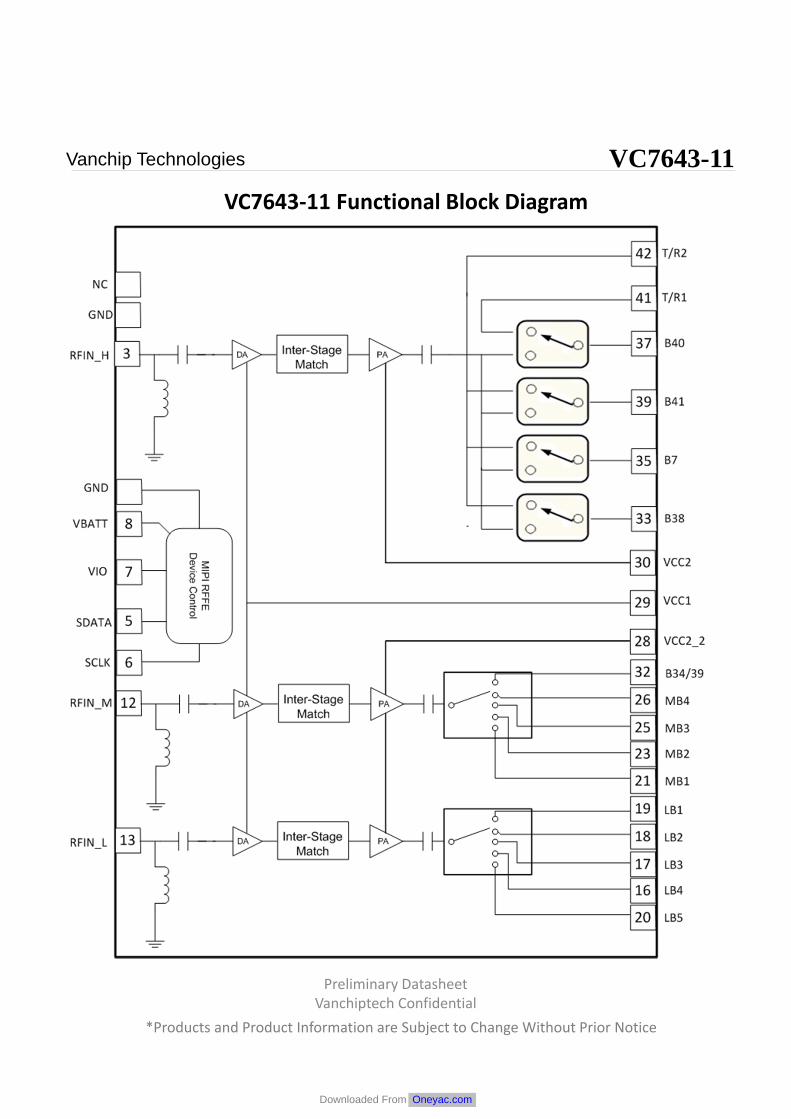
Electrical Characteristics for HIGH FDD‐LTE Mode– Conditions: VCC1=VCC2=VBATT = 3.4V, Ta = 25°C, Zin/Zout = 50ohm– Signal Configuration: 3GPP TS36.101, unless otherwise specified .
FDD‐LTE Band 7VBATT = VCC1 = VCC2 = 3.4 V at Room Temperature +25 °C.
Test LTE signal with QPSK/10MHz/12RBCharacteristics Minimum Typical Maximum Unit Test Condition
Operating Frequency 2500 2535 2570 MHz
Maximum Output Power (Pout_Max) 28 dBm MPR = 0 (3GPP TS36.101)
Gain20 dB Pout=3dBm at Low Gain Mode
28.5 dB Pout=Pout_Max at High Gain Mode
Gain Flatness 0.5 dB High Gain Mode
Relative Gain2 dB Gain at Rx 2620 MHz–2690 MHz
0.5 dB Gain at ISM Band 2400‐2483MHz
17 dB Gain at GPS Band 1574 MHz–1576 MHz
Power Added Efficiency 31 % Pout=Pout_MaxSupply Current 590 mA POUT = Pout_Max, VBATT = 3.4 V
Adjacent Channel Leakage power Ratio‐37 ‐33 dBc ACLR_EUTRA (Pout=Pout_Max)
‐39 ‐36 dBc ACLR1_UTRA
‐43 ‐39 dBc ACLR2_UTRA
Harmonic Suppression‐6 dBm 2nd Harmonic
‐30 dBm 3rd Harmonic
‐40 ‐33 dBm All other harmonics up to 12.75GHz
Tx Noise in Rx Bands*‐126 dBm/Hz Rx Band 2620 MHz–2690 MHz
‐108 dBm/Hz ISM Band 2400‐2483MHz
‐140 dBm/Hz GPS Band 1574 MHz–1577 MHz
EVM 3.5 % Pout = Pout_Max, Load = 50 ohms
Phase Discontinuity Variation ±10 degree
Input VSWR 2.0:1 —Stability (Spurious output) ‐36 dBm At load VSWR = 6:1, all phases, RBW 1MHz,POUT≤28dBm,
Ruggedness 10:1 — No damage or Permanent Degradation at POUT≤28dBm
* Noise power measured with 20MHz/100RB LTE waveform.
*Products and Product Information are Subject to Change Without Prior Notice
Downloaded From Oneyac.com
Preliminary Datasheet Vanchiptech Confidential
VC7643-11Vanchip Technologies
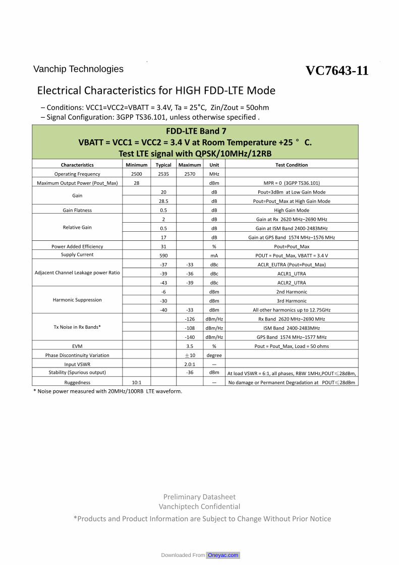
Electrical Characteristics for TDD‐LTE Mode– Conditions: VCC1=VCC2=VBATT = 3.4V, Ta = 25°C, Zin/Zout = 50ohm– Signal Configuration: 3GPP TS36.101, unless otherwise specified .
TDD‐LTE Band 38/41/XGPVBATT = VCC1 = VCC2 = 3.4 V at Room Temperature +25 °C.
Test LTE signal with QPSK/10MHz/12RBCharacteristics Minimum Typical Maximum Unit Test Condition
Operating Frequency 2496 2595 2690 MHz
Maximum Output Power (Pout_Max) 28 dBm MPR = 0 (3GPP TS36.101)
Gain20 dB Pout=3dBm at Low Gain Mode
29 dB Pout=Pout_Max at High Gain Mode
Gain Flatness 0.5 dB High Gain Mode
Relative Gain2.4 dB Gain at ISM Band 2400‐2483MHz
15 dB Gain at GPS Band 1574 MHz–1576 MHz
Power Added Efficiency 30 % Pout=Pout_Max
Supply Current 610 mA POUT = Pout_Max, VBATT = 3.4 V
Adjacent Channel Leakage power Ratio
‐37 ‐33 dBc ACLR_EUTRA (Pout=Pout_Max)
‐39 ‐36 dBc ACLR1_UTRA
‐43 ‐39 dBc ACLR2_UTRA
Harmonic Suppression
‐6 dBm 2nd Harmonic
‐30 dBm 3rd Harmonic
‐40 ‐33 dBm All other harmonics up to 12.75GHz
Tx Noise in Rx Bands*‐106 dBm/Hz ISM Band 2447‐2483MHz
‐140 dBm/Hz GPS Band 1574 MHz–1577 MHz
EVM 3.5 % Pout = Pout_Max, Load = 50 ohms
DC ON/OFF Time 5 us
RF ON/OFF Time 5 us
Input VSWR 2.0:1 —
Stability (Spurious output) ‐36 dBm At load VSWR = 6:1, all phases, RBW 1MHz,POUT≤28dBm,
Ruggedness 10:1 — No damage or Permanent Degradation at POUT≤28dBm
* Noise power measured with 20MHz/100RB LTE waveform.
*Products and Product Information are Subject to Change Without Prior Notice
Downloaded From Oneyac.com

Preliminary Datasheet Vanchiptech Confidential
VC7643-11Vanchip Technologies
Electrical Characteristics for TDD‐LTE Mode– Conditions: VCC1=VCC2=VBATT = 3.4V, Ta = 25°C, Zin/Zout = 50ohm– Signal Configuration: 3GPP TS36.101, unless otherwise specified .
TDD‐LTE Band 40VBATT = VCC1 = VCC2 = 3.4 V at Room Temperature +25 °C.
Test LTE signal with QPSK/10MHz/12RBCharacteristics Minimum Typical Maximum Unit Test Condition
Operating Frequency 2300 2350 2400 MHz
Maximum Output Power (Pout_Max) 28 dBm MPR = 0 (3GPP TS36.101)
Gain20 dB Pout=3dBm at Low Gain Mode
28 dB Pout=Pout_Max at High Gain Mode
Gain Flatness 1 dB High Gain Mode
Relative Gain0.3 dB Gain at ISM Band 2400‐2483MHz
18 dB Gain at GPS Band 1574 MHz–1576 MHz
Power Added Efficiency 31 % Pout=Pout_Max
Supply Current 590 mA POUT = Pout_Max, VBATT = 3.4 V
Adjacent Channel Leakage power Ratio
‐38 ‐33 dBc ACLR_EUTRA (Pout=Pout_Max)
‐40 ‐36 dBc ACLR1_UTRA
‐48 ‐39 dBc ACLR2_UTRA
Harmonic Suppression
‐3 dBm 2nd Harmonic
‐30 dBm 3rd Harmonic
‐40 ‐33 dBm All other harmonics up to 12.75GHz
Tx Noise in Rx Bands*‐106 dBm/Hz ISM Band 2447‐2483MHz
‐140 dBm/Hz GPS Band 1574 MHz–1577 MHz
EVM 5 % Pout = Pout_Max, Load = 50 ohms
DC ON/OFF Time 5 us
RF ON/OFF Time 5 us
Input VSWR 2.0:1 —
Stability (Spurious output) ‐36 dBm At load VSWR = 6:1, all phases, RBW 1MHz,POUT≤28dBm,
Ruggedness 10:1 —No damage or Permanent Degradation at
POUT≤28dBm
* Noise power measured with 20MHz/100RB LTE waveform.
*Products and Product Information are Subject to Change Without Prior Notice
Downloaded From Oneyac.com

Preliminary Datasheet Vanchiptech Confidential
VC7643-11Vanchip Technologies
Electrical Characteristics for MID FDD‐LTE Band Mode– Conditions: VCC1=VCC2=VBATT = 3.4V, Ta = 25°C, Zin/Zout = 50ohm– Signal Configuration: 3GPP TS36.101, unless otherwise specified .
*Products and Product Information are Subject to Change Without Prior Notice
FDD‐LTE Band 1VBATT = VCC1 = VCC2 = 3.4 V at Room Temperature +25 °C.
Test LTE signal with QPSK/10MHz/12RBCharacteristics Minimum Typical Maximum Unit Test Condition
Operating Frequency 1920 1950 1980 MHzMaximum Output Power (Pout_Max) 28 dBm MPR = 0 (3GPP TS36.101)
Gain20 dB Pout=3dBm at Low Gain Mode29.5 dB Pout=Pout_Max at High Gain Mode
Gain Flatness 0.5 dB High Gain Mode
Relative Gain1.5 dB Gain at Rx 2110 MHz–2170 MHz4 dB Gain at ISM Band 2400‐2483MHz1.8 dB Gain at GPS Band 1574 MHz–1576 MHz
Power Added Efficiency 35 % Pout=Pout_MaxSupply Current 520 mA POUT = Pout_Max, VBATT = 3.4 V
Adjacent Channel Leakage power Ratio‐38 ‐33 dBc ACLR_EUTRA (Pout=Pout_Max)‐42 ‐36 dBc ACLR1_UTRA‐57 ‐39 dBc ACLR2_UTRA
Harmonic Suppression‐3 dBm 2nd Harmonic‐25 dBm 3rd Harmonic
‐33 dBm All other harmonics up to 12.75GHz
Tx Noise in Rx Bands‐133 dBm/Hz Rx Band fT+190MHz‐140 dBm/Hz ISM Band 2400‐2483MHz
‐140 dBm/Hz GPS Band 1574 MHz–1577 MHzEVM 5 % Pout = Pout_Max, Load = 50 ohms
Phase Discontinuity Variation ±10 degreeInput Voltage Standing Wave Ratio 2:1 —
Stability (Spurious output) ‐36 dBm At load VSWR = 6:1, all phases, RBW 1MHz, POUT≤28dBm, Ruggedness 10:1 — No damage or Permanent Degradation at POUT≤28dBm
Downloaded From Oneyac.com
Preliminary Datasheet Vanchiptech Confidential
VC7643-11Vanchip Technologies
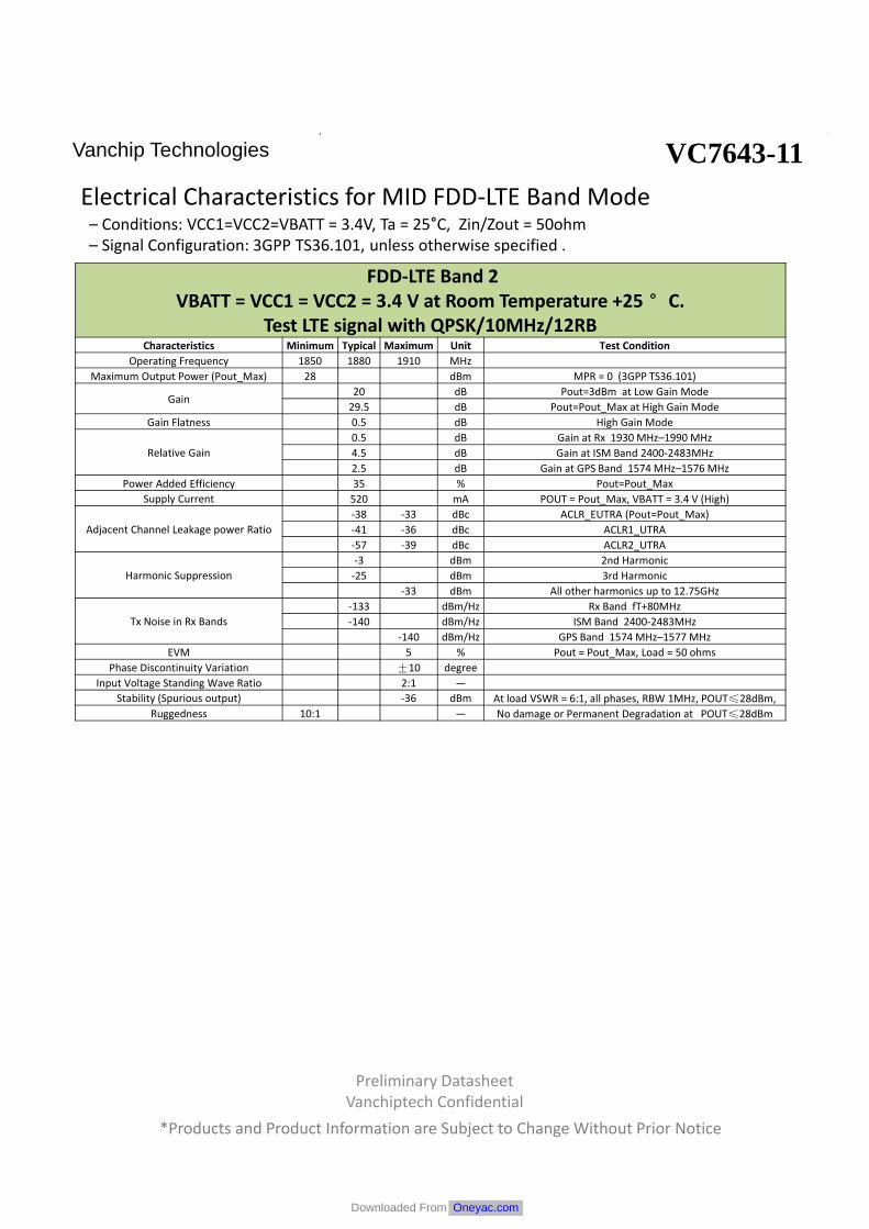
Electrical Characteristics for MID FDD‐LTE Band Mode– Conditions: VCC1=VCC2=VBATT = 3.4V, Ta = 25°C, Zin/Zout = 50ohm– Signal Configuration: 3GPP TS36.101, unless otherwise specified .
*Products and Product Information are Subject to Change Without Prior Notice
FDD‐LTE Band 2VBATT = VCC1 = VCC2 = 3.4 V at Room Temperature +25 °C.
Test LTE signal with QPSK/10MHz/12RBCharacteristics Minimum Typical Maximum Unit Test Condition
Operating Frequency 1850 1880 1910 MHzMaximum Output Power (Pout_Max) 28 dBm MPR = 0 (3GPP TS36.101)
Gain20 dB Pout=3dBm at Low Gain Mode29.5 dB Pout=Pout_Max at High Gain Mode
Gain Flatness 0.5 dB High Gain Mode
Relative Gain0.5 dB Gain at Rx 1930 MHz–1990 MHz4.5 dB Gain at ISM Band 2400‐2483MHz2.5 dB Gain at GPS Band 1574 MHz–1576 MHz
Power Added Efficiency 35 % Pout=Pout_MaxSupply Current 520 mA POUT = Pout_Max, VBATT = 3.4 V (High)
Adjacent Channel Leakage power Ratio‐38 ‐33 dBc ACLR_EUTRA (Pout=Pout_Max)‐41 ‐36 dBc ACLR1_UTRA‐57 ‐39 dBc ACLR2_UTRA
Harmonic Suppression‐3 dBm 2nd Harmonic‐25 dBm 3rd Harmonic
‐33 dBm All other harmonics up to 12.75GHz
Tx Noise in Rx Bands‐133 dBm/Hz Rx Band fT+80MHz‐140 dBm/Hz ISM Band 2400‐2483MHz
‐140 dBm/Hz GPS Band 1574 MHz–1577 MHzEVM 5 % Pout = Pout_Max, Load = 50 ohms
Phase Discontinuity Variation ±10 degreeInput Voltage Standing Wave Ratio 2:1 —
Stability (Spurious output) ‐36 dBm At load VSWR = 6:1, all phases, RBW 1MHz, POUT≤28dBm, Ruggedness 10:1 — No damage or Permanent Degradation at POUT≤28dBm
Downloaded From Oneyac.com

Preliminary Datasheet Vanchiptech Confidential
VC7643-11Vanchip Technologies
– Conditions: VCC1=VCC2=VBATT = 3.4V, Ta = 25°C, Zin/Zout = 50ohm– Signal Configuration: 3GPP TS36.101, unless otherwise specified .
*Products and Product Information are Subject to Change Without Prior Notice
FDD‐LTE Band 3VBATT = VCC1 = VCC2 = 3.4 V at Room Temperature +25 °C.
Test LTE signal with QPSK/10MHz/12RBCharacteristics Minimum Typical Maximum Unit Test Condition
Operating Frequency 1710 1747 1785 MHzMaximum Output Power (Pout_Max) 28 dBm MPR = 0 (3GPP TS36.101)
Gain20 dB Pout=3dBm at Low Gain Mode29.5 dB Pout=Pout_Max at High Gain Mode
Gain Flatness 0.5 dB High Gain Mode
Relative Gain0.2 dB Gain at Rx 1805 MHz–1880 MHz4 dB Gain at ISM Band 2400‐2483MHz2.5 dB Gain at GPS Band 1574 MHz–1576 MHz
Power Added Efficiency 35 % Pout=Pout_MaxSupply Current 520 mA POUT = Pout_Max, VBATT = 3.4 V
Adjacent Channel Leakage power Ratio‐38 ‐33 dBc ACLR_EUTRA (Pout=Pout_Max)‐40 ‐36 dBc ACLR1_UTRA ‐57 ‐39 dBc ACLR2_UTRA
Harmonic Suppression‐3 dBm 2nd Harmonic‐25 dBm 3rd Harmonic
‐33 dBm All other harmonics up to 12.75GHz
Tx Noise in Rx Bands‐133 dBm/Hz Rx Band fT+95MHz‐140 dBm/Hz ISM Band 2400‐2483MHz‐140 dBm/Hz GPS Band 1574 MHz–1577 MHz
EVM 5 % Pout = Pout_Max, Load = 50 ohmsPhase Discontinuity Variation ±10 degree
Input Voltage Standing Wave Ratio 1.2:1 2:1 —Stability (Spurious output) ‐36 dBm At load VSWR = 6:1, all phases, RBW 1MHz,POUT≤28dBm,
Ruggedness 10:1 — No damage or Permanent Degradation at POUT≤28dBm
Electrical Characteristics for MID FDD‐LTE Band Mode
Downloaded From Oneyac.com

Preliminary Datasheet Vanchiptech Confidential
VC7643-11Vanchip Technologies
– Conditions: VCC1=VCC2=VBATT = 3.4V, Ta = 25°C, Zin/Zout = 50ohm– Signal Configuration: 3GPP TS36.101, unless otherwise specified .
*Products and Product Information are Subject to Change Without Prior Notice
FDD‐LTE Band 4VBATT = VCC1 = VCC2 = 3.4 V at Room Temperature +25 °C.
Test LTE signal with QPSK/10MHz/12RBCharacteristics Minimum Typical Maximum Unit Test Condition
Operating Frequency 1710 1737.5 1755 MHzMaximum Output Power (Pout_Max) 28 dBm MPR = 0 (3GPP TS36.101)
Gain20 dB Pout=3dBm at Low Gain Mode29 dB Pout=Pout_Max at High Gain Mode
Gain Flatness 0.5 dB High Gain Mode
Relative Gain0.2 dB Gain at Rx 1805 MHz–1880 MHz4 dB Gain at ISM Band 2400‐2483MHz2.5 dB Gain at GPS Band 1574 MHz–1576 MHz
Power Added Efficiency 36 % Pout=Pout_MaxSupply Current 520 mA POUT = Pout_Max, VBATT = 3.4 V
Adjacent Channel Leakage power Ratio‐39 ‐33 dBc ACLR_EUTRA (Pout=Pout_Max)‐39 ‐36 dBc ACLR1_UTRA ‐57 ‐39 dBc ACLR2_UTRA
Harmonic Suppression‐3 dBm 2nd Harmonic‐25 dBm 3rd Harmonic
‐33 dBm All other harmonics up to 12.75GHz
Tx Noise in Rx Bands‐133 dBm/Hz Rx Band fT+400MHz‐140 dBm/Hz ISM Band 2400‐2483MHz‐140 dBm/Hz GPS Band 1574 MHz–1577 MHz
EVM 5 % Pout = Pout_Max, Load = 50 ohmsPhase Discontinuity Variation ±10 degree
Input Voltage Standing Wave Ratio 1.2:1 2:1 —Stability (Spurious output) ‐36 dBm At load VSWR = 6:1, all phases, RBW 1MHz,POUT≤28dBm,
Ruggedness 10:1 — No damage or Permanent Degradation at POUT≤28dBm
Electrical Characteristics for MID FDD‐LTE Band Mode
Downloaded From Oneyac.com

Preliminary Datasheet Vanchiptech Confidential
VC7643-11Vanchip Technologies
– Conditions: VCC1=VCC2=VBATT = 3.4V, Ta = 25°C, Zin/Zout = 50ohm– Signal Configuration: 3GPP TS36.101, unless otherwise specified .
*Products and Product Information are Subject to Change Without Prior Notice
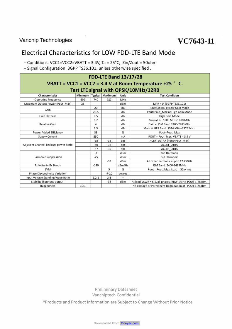
Electrical Characteristics for LOW FDD‐LTE Band Mode
FDD‐LTE Band5VBATT = VCC1 = VCC2 = 3.4 V at Room Temperature +25 °C.
Test LTE signal with QPSK/10MHz/12RBCharacteristics Minimum Typical Maximum Unit Test Condition
Operating Frequency 824 836 849 MHzMaximum Output Power (Pout_Max) 28 dBm MPR = 0 (3GPP TS36.101)
Gain20 dB Pout=3dBm at Low Gain Mode28 dB Pout=Pout_Max at High Gain Mode
Gain Flatness 0.5 dB High Gain Mode
Relative Gain0.5 dB Gain at Rx 869 MHz–894 MHz37 dB Gain at ISM Band 2400‐2483MHz25 dB Gain at GPS Band 1574 MHz–1576 MHz
Power Added Efficiency 34 % Pout=Pout_MaxSupply Current 530 mA POUT = Pout_Max, VBATT = 3.4 V
Adjacent Channel Leakage power Ratio‐40 ‐33 dBc ACLR_EUTRA (Pout=Pout_Max)‐41 ‐36 dBc ACLR1_UTRA ‐64 ‐39 dBc ACLR2_UTRA
Harmonic Suppression‐9 dBm 2nd Harmonic‐20 dBm 3rd Harmonic
‐33 dBm All other harmonics up to 12.75GHz
Tx Noise in Rx Bands‐133 dBm/Hz Rx Band fT+45MHz‐140 dBm/Hz ISM Band 2400‐2483MHz‐140 dBm/Hz GPS Band 1574 MHz–1577 MHz
EVM 5 % Pout = Pout_Max, Load = 50 ohmsPhase Discontinuity Variation ±10 degree
Input Voltage Standing Wave Ratio 2:1 —Stability (Spurious output) ‐36 dBm At load VSWR = 6:1, all phases, RBW 1MHz,POUT≤28dBm,
Ruggedness 10:1 — No damage or Permanent Degradation at POUT≤28dBm
Downloaded From Oneyac.com

Preliminary Datasheet Vanchiptech Confidential
VC7643-11Vanchip Technologies
Electrical Characteristics for LOW FDD‐LTE Mode– Conditions: VCC1=VCC2=VBATT = 3.4V, Ta = 25°C, Zin/Zout = 50ohm– Signal Configuration: 3GPP TS36.101, unless otherwise specified .
*Products and Product Information are Subject to Change Without Prior Notice
FDD‐LTE Band8VBATT = VCC1 = VCC2 = 3.4 V at Room Temperature +25 °C.
Test LTE signal with QPSK/10MHz/12RBCharacteristics Minimum Typical Maximum Unit Test Condition
Operating Frequency 880 897 915 MHzMaximum Output Power (Pout_Max) 28 dBm MPR = 0 (3GPP TS36.101)
Gain20 dB Pout=3dBm at Low Gain Mode28 dB Pout=Pout_Max at High Gain Mode
Gain Flatness 0.5 dB High Gain Mode
Relative Gain0.5 dB Gain at Rx 925 MHz–960 MHz36 dB Gain at ISM Band 2400‐2483MHz24 dB Gain at GPS Band 1574 MHz–1576 MHz
Power Added Efficiency 35 % Pout=Pout_MaxSupply Current 530 mA POUT = Pout_Max, VBATT = 3.4 V
Adjacent Channel Leakage power Ratio‐38 ‐33 dBc ACLR_EUTRA (Pout=Pout_Max)‐40 ‐36 dBc ACLR1_UTRA ‐63 ‐39 dBc ACLR2_UTRA
Harmonic Suppression‐9 dBm 2nd Harmonic‐20 dBm 3rd Harmonic
‐33 dBm All other harmonics up to 12.75GHz
Tx Noise in Rx Bands‐133 dBm/Hz Rx Band fT+45MHz‐140 dBm/Hz ISM Band 2400‐2483MHz‐140 dBm/Hz GPS Band 1574 MHz–1577 MHz
EVM 5 % Pout = Pout_Max, Load = 50 ohmsPhase Discontinuity Variation ±10 degree
Input Voltage Standing Wave Ratio 2:1 —Stability (Spurious output) ‐36 dBm At load VSWR = 6:1, all phases, RBW 1MHz, POUT≤28dBm,
Ruggedness 10:1 — No damage or Permanent Degradation at POUT≤28dBm
Downloaded From Oneyac.com

Preliminary Datasheet Vanchiptech Confidential
VC7643-11Vanchip Technologies
– Conditions: VCC1=VCC2=VBATT = 3.4V, Ta = 25°C, Zin/Zout = 50ohm– Signal Configuration: 3GPP TS36.101, unless otherwise specified .
*Products and Product Information are Subject to Change Without Prior Notice
FDD‐LTE Band 20VBATT = VCC1 = VCC2 = 3.4 V at Room Temperature +25 °C.
Test LTE signal with QPSK/10MHz/12RBCharacteristics Minimum Typical Maximum Unit Test Condition
Operating Frequency 832 847 862 MHzMaximum Output Power (Pout_Max) 28 dBm MPR = 0 (3GPP TS36.101)
Gain20 dB Pout=3dBm at Low Gain Mode28 dB Pout=Pout_Max at High Gain Mode
Gain Flatness 0.5 dB High Gain Mode
Relative Gain0.2 dB Gain at Rx 1805 MHz–1880 MHz4 dB Gain at ISM Band 2400‐2483MHz2.5 dB Gain at GPS Band 1574 MHz–1576 MHz
Power Added Efficiency 34 % Pout=Pout_MaxSupply Current 530 mA POUT = Pout_Max, VBATT = 3.4 V
Adjacent Channel Leakage power Ratio‐39 ‐33 dBc ACLR_EUTRA (Pout=Pout_Max)‐40 ‐36 dBc ACLR1_UTRA‐57 ‐39 dBc ACLR2_UTRA
Harmonic Suppression‐3 dBm 2nd Harmonic‐25 dBm 3rd Harmonic
‐33 dBm All other harmonics up to 12.75GHz
Tx Noise in Rx Bands‐133 dBm/Hz Rx Band fT‐41MHz‐140 dBm/Hz ISM Band 2400‐2483MHz‐140 dBm/Hz GPS Band 1574 MHz–1577 MHz
EVM 5 % Pout = Pout_Max, Load = 50 ohmsPhase Discontinuity Variation ±10 degree
Input Voltage Standing Wave Ratio 1.2:1 2:1 —Stability (Spurious output) ‐36 dBm At load VSWR = 6:1, all phases, RBW 1MHz, POUT≤28dBm,
Ruggedness 10:1 — No damage or Permanent Degradation at POUT≤28dBm
Electrical Characteristics for LOW FDD‐LTE Band Mode
Downloaded From Oneyac.com
Preliminary Datasheet Vanchiptech Confidential
VC7643-11Vanchip Technologies
– Conditions: VCC1=VCC2=VBATT = 3.4V, Ta = 25°C, Zin/Zout = 50ohm– Signal Configuration: 3GPP TS36.101, unless otherwise specified .
*Products and Product Information are Subject to Change Without Prior Notice
FDD‐LTE Band 13/17/28VBATT = VCC1 = VCC2 = 3.4 V at Room Temperature +25 °C.
Test LTE signal with QPSK/10MHz/12RBCharacteristics Minimum Typical Maximum Unit Test Condition
Operating Frequency 699 740 787 MHzMaximum Output Power (Pout_Max) 28 dBm MPR = 0 (3GPP TS36.101)
Gain20 dB Pout=3dBm at Low Gain Mode28.5 dB Pout=Pout_Max at High Gain Mode
Gain Flatness 0.5 dB High Gain Mode
Relative Gain0.2 dB Gain at Rx 1805 MHz–1880 MHz4 dB Gain at ISM Band 2400‐2483MHz2.5 dB Gain at GPS Band 1574 MHz–1576 MHz
Power Added Efficiency 33 % Pout=Pout_MaxSupply Current 550 mA POUT = Pout_Max, VBATT = 3.4 V
Adjacent Channel Leakage power Ratio‐38 ‐33 dBc ACLR_EUTRA (Pout=Pout_Max)‐40 ‐36 dBc ACLR1_UTRA‐57 ‐39 dBc ACLR2_UTRA
Harmonic Suppression‐3 dBm 2nd Harmonic‐25 dBm 3rd Harmonic
‐33 dBm All other harmonics up to 12.75GHzTx Noise in Rx Bands ‐140 dBm/Hz ISM Band 2400‐2483MHz
EVM 5 % Pout = Pout_Max, Load = 50 ohmsPhase Discontinuity Variation ±10 degree
Input Voltage Standing Wave Ratio 1.2:1 2:1 —Stability (Spurious output) ‐36 dBm At load VSWR = 6:1, all phases, RBW 1MHz, POUT≤28dBm,
Ruggedness 10:1 — No damage or Permanent Degradation at POUT≤28dBm
Electrical Characteristics for LOW FDD‐LTE Band Mode
Downloaded From Oneyac.com

Preliminary Datasheet Vanchiptech Confidential
VC7643-11Vanchip Technologies
Electrical Characteristics for WCDMA MID‐Band Mode– Conditions: VCC1=VCC2=VBATT = 3.4V, Ta = 25°C, Zin/Zout = 50ohm– Signal Configuration: WCDMA(R99) WCDMA Voice Mode (Uplink Reference Measurement Channel: 12.2 kbps)
*Products and Product Information are Subject to Change Without Prior Notice
WCDMA Band1VBATT = VCC1 = VCC2 = 3.4 V at Room Temperature +25 °C.
Characteristics Minimum Typical Maximum Unit Test ConditionOperating Frequency 1920 1950 1980 MHz
Maximum Output Power (Pout_Max) 28 dBm
Gain20 dB Pout=3dBm at Low Gain Mode29.5 dB Pout=Pout_Max at High Gain Mode
Gain Flatness 0.5 dB High Gain Mode
Relative Gain1.5 dB Gain at Rx 2110MHz–2170 MHz4 dB Gain at ISM Band 2400‐2483MHz1.8 dB Gain at GPS Band 1574 MHz–1576 MHz
Power Added Efficiency 35 % Pout=Pout_MaxSupply Current 510 mA POUT = Pout_Max, VBATT = 3.4 V
Adjacent Channel Leakage power Ratio
‐45 ‐38 dBc ACLR1_UTRA‐56 ‐48 dBc ACLR2_UTRA
Harmonic Suppression‐3 dBm 2nd Harmonic‐25 dBm 3rd Harmonic
‐33 dBm All other harmonics up to 12.75GHz
Tx Noise in Rx Bands‐133 dBm/Hz Rx Band fT+190MHz‐141 dBm/Hz ISM Band 2400‐2483MHz‐141 dBm/Hz GPS Band 1574 MHz–1577 MHz
EVM 5 % Pout = Pout_Max, Load = 50 ohmsPhase Discontinuity Variation ±10 degree
Input Voltage Standing Wave Ratio 2:1 —Stability (Spurious output) ‐36 dBm At load VSWR = 6:1, all phases, RBW 1MHz, POUT≤28dBm,
Ruggedness 10:1 — No damage or Permanent Degradation at POUT≤28dBm
Downloaded From Oneyac.com

Preliminary Datasheet Vanchiptech Confidential
VC7643-11Vanchip Technologies
Electrical Characteristics for WCDMA MID‐Band Mode– Conditions: VCC1=VCC2=VBATT = 3.4V, Ta = 25°C, Zin/Zout = 50ohm– Signal Configuration: WCDMA(R99) WCDMA Voice Mode (Uplink Reference Measurement Channel: 12.2 kbps)
*Products and Product Information are Subject to Change Without Prior Notice
WCDMA Band2VBATT = VCC1 = VCC2 = 3.4 V at Room Temperature +25 °C.
Characteristics Minimum Typical Maximum Unit Test ConditionOperating Frequency 1850 1880 1910 MHz
Maximum Output Power (Pout_Max) 28 dBm
Gain25 dB Pout=3dBm at Low Gain Mode29.5 dB Pout=Pout_Max at High Gain Mode
Gain Flatness 0.5 dB High Gain Mode
Relative Gain0.5 dB Gain at Rx 1930 MHz–1990 MHz4.5 dB Gain at ISM Band 2400‐2483MHz2.5 dB Gain at GPS Band 1574 MHz–1576 MHz
Power Added Efficiency 37 % Pout=Pout_MaxSupply Current 500 mA POUT = Pout_Max, VBATT = 3.4 V
Adjacent Channel Leakage power Ratio‐45 ‐38 dBc ACLR1_UTRA‐56 ‐48 dBc ACLR2_UTRA
Harmonic Suppression‐3 dBm 2nd Harmonic‐25 dBm 3rd Harmonic
‐33 dBm All other harmonics up to 12.75GHz
Tx Noise in Rx Bands‐133 dBm/Hz Rx Band fT+80MHz‐141 dBm/Hz ISM Band 2400‐2483MHz‐141 ‐140 dBm/Hz GPS Band 1574 MHz–1577 MHz
EVM 5 % Pout = Pout_Max, Load = 50 ohmsPhase Discontinuity Variation ±10 degree
Input Voltage Standing Wave Ratio 2:1 —Stability (Spurious output) ‐36 dBm At load VSWR = 6:1, all phases, RBW 1MHz, POUT≤28dBm,
Ruggedness 10:1 — No damage or Permanent Degradation at POUT≤28dBm
Downloaded From Oneyac.com

Preliminary Datasheet Vanchiptech Confidential
VC7643-11Vanchip Technologies
Electrical Characteristics for WCDMA MID‐Band Mode– Conditions: VCC1=VCC2=VBATT = 3.4V, Ta = 25°C, Zin/Zout = 50ohm– Signal Configuration: WCDMA(R99) WCDMA Voice Mode (Uplink Reference Measurement Channel: 12.2 kbps)
*Products and Product Information are Subject to Change Without Prior Notice
WCDMA Band3VBATT = VCC1 = VCC2 = 3.4 V at Room Temperature +25 °C.
Characteristics Minimum Typical Maximum Unit Test ConditionOperating Frequency 1710 1747 1785 MHz
Maximum Output Power (Pout_Max) 28.5 dBm
Gain25 dB Pout=3dBm at Low Gain Mode29 dB Pout=Pout_Max at High Gain Mode
Gain Flatness 0.5 dB High Gain Mode
Relative Gain0.2 dB Gain at Rx 1805 MHz–1880 MHz4 dB Gain at ISM Band 2400‐2483MHz2.5 dB Gain at GPS Band 1574 MHz–1576 MHz
Power Added Efficiency 36 % Pout=Pout_MaxSupply Current 510 mA POUT = Pout_Max, VBATT = 3.4 V
Adjacent Channel Leakage power Ratio‐45 ‐38 dBc ACLR1_UTRA‐55 ‐48 dBc ACLR2_UTRA
Harmonic Suppression‐3 dBm 2nd Harmonic‐25 dBm 3rd Harmonic
‐33 dBm All other harmonics up to 12.75GHz
Tx Noise in Rx Bands‐133 dBm/Hz Rx Band fT+95MHz‐140 dBm/Hz ISM Band 2400‐2483MHz‐140 dBm/Hz GPS Band 1574 MHz–1577 MHz
EVM 5 % Pout = Pout_Max, Load = 50 ohmsPhase Discontinuity Variation ±10 degree
Input Voltage Standing Wave Ratio 2:1 —Stability (Spurious output) ‐36 dBm At load VSWR = 6:1, all phases, RBW 1MHz, POUT≤28dBm,
Ruggedness 10:1 — No damage or Permanent Degradation at POUT≤28dBm
Downloaded From Oneyac.com

Preliminary Datasheet Vanchiptech Confidential
VC7643-11Vanchip Technologies
Electrical Characteristics for WCDMA MID‐Band Mode– Conditions: VCC1=VCC2=VBATT = 3.4V, Ta = 25°C, Zin/Zout = 50ohm– Signal Configuration: WCDMA(R99) WCDMA Voice Mode (Uplink Reference Measurement Channel: 12.2 kbps)
*Products and Product Information are Subject to Change Without Prior Notice
WCDMA Band4VBATT = VCC1 = VCC2 = 3.4 V at Room Temperature +25 °C.
Characteristics Minimum Typical Maximum Unit Test ConditionOperating Frequency 1710 1737.5 1755 MHz
Maximum Output Power (Pout_Max) 28 dBm
Gain25 dB Pout=3dBm at Low Gain Mode29 dB Pout=Pout_Max at High Gain Mode
Gain Flatness 0.5 dB High Gain Mode
Relative Gain0.2 dB Gain at Rx 1805 MHz–1880 MHz4 dB Gain at ISM Band 2400‐2483MHz2.5 dB Gain at GPS Band 1574 MHz–1576 MHz
Power Added Efficiency 36 % Pout=Pout_MaxSupply Current 510 mA POUT = Pout_Max, VBATT = 3.4 V
Adjacent Channel Leakage power Ratio‐45 ‐38 dBc ACLR1_UTRA‐55 ‐48 dBc ACLR2_UTRA
Harmonic Suppression‐3 dBm 2nd Harmonic‐25 dBm 3rd Harmonic
‐33 dBm All other harmonics up to 12.75GHz
Tx Noise in Rx Bands‐133 dBm/Hz Rx Band fT+400MHz‐140 dBm/Hz ISM Band 2400‐2483MHz‐140 dBm/Hz GPS Band 1574 MHz–1577 MHz
EVM 5 % Pout = Pout_Max, Load = 50 ohmsPhase Discontinuity Variation ±10 degree
Input Voltage Standing Wave Ratio 2:1 —Stability (Spurious output) ‐36 dBm At load VSWR = 6:1, all phases, RBW 1MHz, POUT≤28dBm,
Ruggedness 10:1 — No damage or Permanent Degradation at POUT≤28dBm
Downloaded From Oneyac.com

Preliminary Datasheet Vanchiptech Confidential
VC7643-11Vanchip Technologies
Electrical Characteristics for WCDMA LOW‐Band Mode– Conditions: VCC1=VCC2=VBATT = 3.4V, Ta = 25°C, Zin/Zout = 50ohm– Signal Configuration: WCDMA(R99) WCDMA Voice Mode (Uplink Reference Measurement Channel: 12.2 kbps)
*Products and Product Information are Subject to Change Without Prior Notice
WCDMA Band5VBATT = VCC1 = VCC2 = 3.4 V at Room Temperature +25 °C.
Characteristics Minimum Typical Maximum Unit Test ConditionOperating Frequency 824 836 849 MHz
Maximum Output Power (Pout_Max) 28 dBm
Gain25 dB Pout=3dBm at Low Gain Mode28 dB Pout=Pout_Max at High Gain Mode
Gain Flatness 0.5 dB High Gain Mode
Relative Gain0.5 dB Gain at Rx 869 MHz–894 MHz37 dB Gain at ISM Band 2400‐2483MHz25 dB Gain at GPS Band 1574 MHz–1576 MHz
Power Added Efficiency 36 % Pout=Pout_MaxSupply Current 510 mA POUT = Pout_Max, VBATT = 3.4 V
Adjacent Channel Leakage power Ratio‐42 ‐38 dBc ACLR1_UTRA‐59 ‐48 dBc ACLR2_UTRA
Harmonic Suppression‐12 dBm 2nd Harmonic‐20 dBm 3rd Harmonic
‐33 dBm All other harmonics up to 12.75GHz
Tx Noise in Rx Bands‐133 dBm/Hz Rx Band fT+45MHz‐141 dBm/Hz ISM Band 2400‐2483MHz‐141 dBm/Hz GPS Band 1574 MHz–1577 MHz
EVM 5 % Pout = Pout_Max, Load = 50 ohmsPhase Discontinuity Variation ±10 degree
Input Voltage Standing Wave Ratio 2:1 —Stability (Spurious output) ‐37 dBm At load VSWR = 6:1, all phases, RBW 1MHz, POUT≤28dBm,
Ruggedness 10:1 — No damage or Permanent Degradation at POUT≤28dBm
Downloaded From Oneyac.com

Preliminary Datasheet Vanchiptech Confidential
VC7643-11Vanchip Technologies
Electrical Characteristics for WCDMA LOW‐Band Mode– Conditions: VCC1=VCC2=VBATT = 3.4V, Ta = 25°C, Zin/Zout = 50ohm– Signal Configuration: WCDMA(R99) WCDMA Voice Mode (Uplink Reference Measurement Channel: 12.2 kbps)
*Products and Product Information are Subject to Change Without Prior Notice
WCDMA Band8VBATT = VCC1 = VCC2 = 3.4 V at Room Temperature +25 °C.
Characteristics Minimum Typical Maximum Unit Test ConditionOperating Frequency 880 897 915 MHz
Maximum Output Power (Pout_Max) 28 dBm
Gain25 dB Pout=3dBm at Low Gain Mode28 dB Pout=Pout_Max at High Gain Mode
Gain Flatness 0.5 dB High Gain Mode
Relative Gain0.5 dB Gain at Rx 925 MHz–960 MHz36 dB Gain at ISM Band 2400‐2483MHz24 dB Gain at GPS Band 1574 MHz–1576 MHz
Power Added Efficiency 35 % Pout=Pout_MaxSupply Current 500 mA POUT = Pout_Max, VBATT = 3.4 V
Adjacent Channel Leakage power Ratio‐45 ‐38 dBc ACLR1_UTRA‐60 ‐48 dBc ACLR2_UTRA
Harmonic Suppression‐9 dBm 2nd Harmonic‐20 dBm 3rd Harmonic
‐33 dBm All other harmonics up to 12.75GHz
Tx Noise in Rx Bands‐133 dBm/Hz Rx Band fT+45MHz‐141 dBm/Hz ISM Band 2400‐2483MHz‐141 dBm/Hz GPS Band 1574 MHz–1577 MHz
EVM 5 % Pout = Pout_Max, Load = 50 ohmsPhase Discontinuity Variation ±10 degree
Input Voltage Standing Wave Ratio 2:1 —Stability (Spurious output) ‐36 dBm At load VSWR = 6:1, all phases, RBW 1MHz,POUT≤28dBm,
Ruggedness 10:1 — No damage or Permanent Degradation at POUT≤28dBm
Downloaded From Oneyac.com

Preliminary Datasheet Vanchiptech Confidential
VC7643-11Vanchip Technologies
Electrical Characteristics for TDD‐LTE Mode– Conditions: VCC1=VCC2=VBATT = 3.4V, Ta = 25°C, Zin/Zout = 50ohm– Signal Configuration: 3GPP TS36.101, unless otherwise specified .
TDD‐LTE Band 39VBATT = VCC1 = VCC2 = 3.4 V at Room Temperature +25 °C.
Test LTE signal with QPSK/10MHz/12RBCharacteristics Minimum Typical Maximum Unit Test Condition
Operating Frequency 1880 1900 1920 MHz
Maximum Output Power (Pout_Max) 28 dBm MPR = 0 (3GPP TS36.101)
Gain 26 dB Pout=Pout_Max
Gain Flatness 0.5 dB
Power Added Efficiency 35 % Pout=Pout_Max
Supply Current 520 mA POUT = Pout_Max, VBATT = 3.4 V
Adjacent Channel Leakage power Ratio
‐39 ‐33 dBc ACLR_EUTRA (Pout=Pout_Max)
‐40 ‐36 dBc ACLR1_UTRA
‐48 ‐41 dBc ACLR2_UTRA
Harmonic Suppression
‐5 dBm 2nd Harmonic
‐28 dBm 3rd Harmonic
‐33 dBm All other harmonics up to 12.75GHz
EVM 3.5 % Pout = Pout_Max, Load = 50 ohms
DC ON/OFF Time 5 us
RF ON/OFF Time 5 us
Input VSWR 2.0:1 —
Stability (Spurious output) ‐36 dBm At load VSWR = 6:1, all phases, RBW 1MHz,POUT≤28dBm,
Ruggedness 10:1 — No damage or Permanent Degradation at POUT≤28dBm
*Products and Product Information are Subject to Change Without Prior Notice
Downloaded From Oneyac.com
Preliminary Datasheet Vanchiptech Confidential
VC7643-11Vanchip Technologies
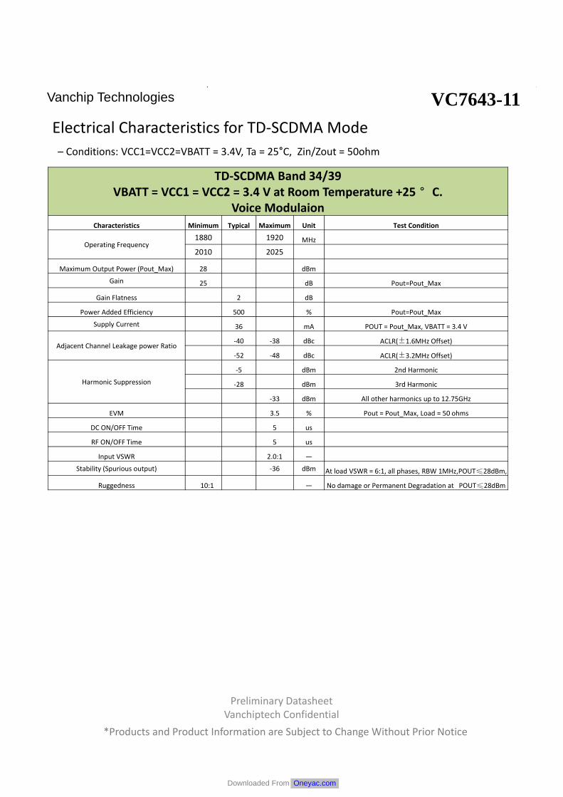
Electrical Characteristics for TD‐SCDMA Mode– Conditions: VCC1=VCC2=VBATT = 3.4V, Ta = 25°C, Zin/Zout = 50ohm
TD‐SCDMA Band 34/39VBATT = VCC1 = VCC2 = 3.4 V at Room Temperature +25 °C.
Voice ModulaionCharacteristics Minimum Typical Maximum Unit Test Condition
Operating Frequency1880 1920 MHz
2010 2025
Maximum Output Power (Pout_Max) 28 dBm
Gain 25 dB Pout=Pout_Max
Gain Flatness 2 dB
Power Added Efficiency 500 % Pout=Pout_Max
Supply Current 36 mA POUT = Pout_Max, VBATT = 3.4 V
Adjacent Channel Leakage power Ratio‐40 ‐38 dBc ACLR(±1.6MHz Offset)
‐52 ‐48 dBc ACLR(±3.2MHz Offset)
Harmonic Suppression
‐5 dBm 2nd Harmonic
‐28 dBm 3rd Harmonic
‐33 dBm All other harmonics up to 12.75GHz
EVM 3.5 % Pout = Pout_Max, Load = 50 ohms
DC ON/OFF Time 5 us
RF ON/OFF Time 5 us
Input VSWR 2.0:1 —
Stability (Spurious output) ‐36 dBm At load VSWR = 6:1, all phases, RBW 1MHz,POUT≤28dBm,
Ruggedness 10:1 — No damage or Permanent Degradation at POUT≤28dBm
*Products and Product Information are Subject to Change Without Prior Notice
Downloaded From Oneyac.com
Preliminary Datasheet Vanchiptech Confidential
VC7643-11Vanchip Technologies
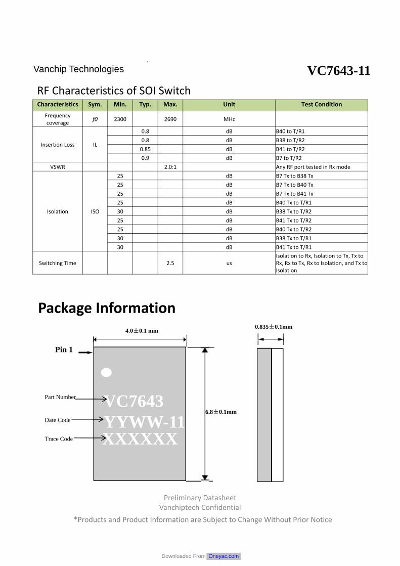
RF Characteristics of SOI SwitchCharacteristics Sym. Min. Typ. Max. Unit Test Condition
Frequency coverage f0 2300 2690 MHz
Insertion Loss IL
0.8 dB B40 to T/R1 0.8 dB B38 to T/R2 0.85 dB B41 to T/R2 0.9 dB B7 to T/R2
VSWR 2.0:1 Any RF port tested in Rx mode
Isolation ISO
25 dB B7 Tx to B38 Tx 25 dB B7 Tx to B40 Tx 25 dB B7 Tx to B41 Tx 25 dB B40 Tx to T/R1 30 dB B38 Tx to T/R2 25 dB B41 Tx to T/R2 25 dB B40 Tx to T/R2 30 dB B38 Tx to T/R1 30 dB B41 Tx to T/R1
Switching Time 2.5 usIsolation to Rx, Isolation to Tx, Tx to Rx, Rx to Tx, Rx to Isolation, and Tx to Isolation
*Products and Product Information are Subject to Change Without Prior Notice
6.8±0.1mm
Part Number
Date Code
Trace Code
VC7643YYWW-11XXXXXX
Pin 1
4.0±0.1 mm 0.835±0.1mm
Package Information
Downloaded From Oneyac.com

Preliminary Datasheet Vanchiptech Confidential
VC7643-11Vanchip Technologies
Pad layout as seen from Top View looking through package
Pin illustration and DescriptionGND
GND
GNDB4
0
B41
T/R1
T/R2
VBATT
VIO
RFIN_H
GND
GND
SDATA
NC
SCLK
VCC1
VCC2
GND
B7
B34/39
B38
GND
*Products and Product Information are Subject to Change Without Prior Notice
GND
GND
GND
GND
GND
GND
LB2
LB5
MB1
LB1
LB3
LB4
GND
GND
NC
NC
RFIN_M
NC
RFIN_L
VCC2_2
GND
MB4
GND
GND
MB3
MB2
GND PAD
GND PAD
Pin # Symbol Description3 RFIN_H High Band (HB) RF Signal Input 4 NC No Connect5 SDATA MIPI Data 6 SCLK MIPI Clock 7 VIO MIPI Supply8 VBATT Battery Supply9 NC No Connect10 NC No Connect11 NC No Connect12 RFIN_M Mid Band (MB) RF Signal Input 13 RFIN_L Low Band (LB) RF Signal Input 16 LB4 LB 4 RF OUT 17 LB3 LB 3 RF OUT 18 LB2 LB 2 RF OUT 19 LB1 LB 1 RF OUT 20 LB5 LB 5 RF OUT 21 MB1 MB 1 RF OUT 23 MB2 MB 2 RF OUT 25 MB3 MB 3 RF OUT 26 MB4 MB 4 RF OUT 28 VCC2_2 MB/LB 2nd Stage PA Collector Supply 29 VCC1 HB/MB/LB 1st Stage PA Collector Supply30 VCC2 HB Stage2 PA Collector Supply 32 B34/39 Bands 34/39 RF OUT 33 B38 Band 38 RF OUT 35 B7 Band 7 RF OUT 37 B40 Band 40 RF OUT 39 B41 Band 41 RF OUT41 T/R1 B40 Rx Port42 T/R2 B7/B38/B41 Rx PortGround Pin 1,2,14,15,22,24,27,31,34,36,38,40Ground PAD Ground Pad is Module Underside
Downloaded From Oneyac.com

Preliminary Datasheet Vanchiptech Confidential
VC7643-11Vanchip Technologies
Package Outline (Unit: mm)
*Products and Product Information are Subject to Change Without Prior Notice
Downloaded From Oneyac.com

Preliminary Datasheet Vanchiptech Confidential
EVB Schematic Diagram
VC7643-11Vanchip Technologies
Note:1. ALL RF Input and output Trace with 50 Ohm Microstrip‐line.2. RF OUTPUT DC‐Block less.
*Products and Product Information are Subject to Change Without Prior Notice
Downloaded From Oneyac.com
Preliminary Datasheet Vanchiptech Confidential
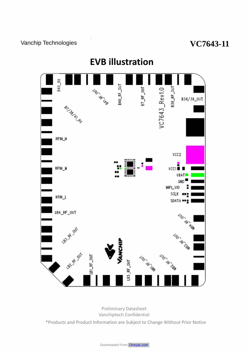
VC7643-11
EVB illustration
Vanchip Technologies
*Products and Product Information are Subject to Change Without Prior Notice
Downloaded From Oneyac.com
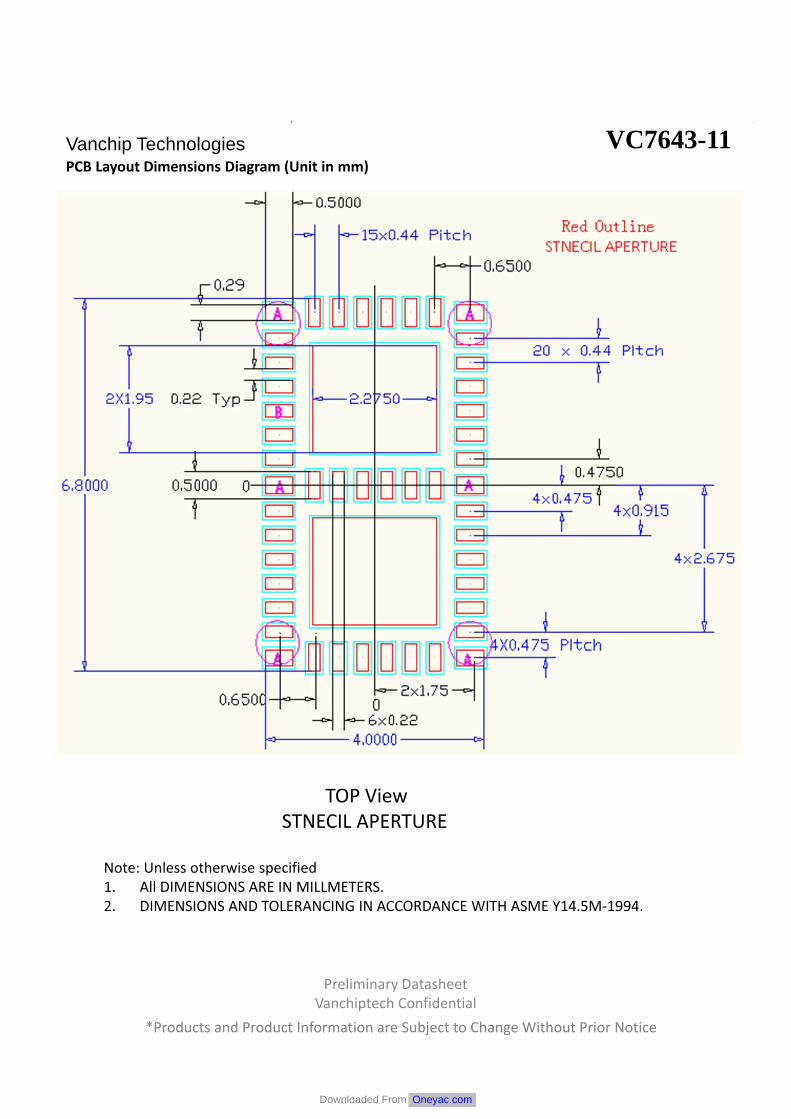
Preliminary Datasheet Vanchiptech Confidential
VC7643-11Vanchip TechnologiesPCB Layout Dimensions Diagram (Unit in mm)
*Products and Product Information are Subject to Change Without Prior Notice
Note: Unless otherwise specified1. All DIMENSIONS ARE IN MILLMETERS.2. DIMENSIONS AND TOLERANCING IN ACCORDANCE WITH ASME Y14.5M‐1994.
TOP ViewSTNECIL APERTURE
Downloaded From Oneyac.com
Preliminary Datasheet Vanchiptech Confidential
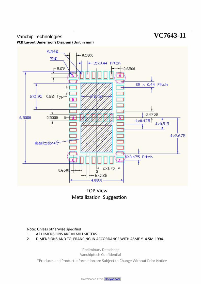
VC7643-11Vanchip TechnologiesPCB Layout Dimensions Diagram (Unit in mm)
*Products and Product Information are Subject to Change Without Prior Notice
Note: Unless otherwise specified1. All DIMENSIONS ARE IN MILLMETERS.2. DIMENSIONS AND TOLERANCING IN ACCORDANCE WITH ASME Y14.5M‐1994.
TOP ViewMetallization Suggestion
Downloaded From Oneyac.com

Preliminary Datasheet Vanchiptech Confidential
VC7643-11Vanchip TechnologiesPCB Layout Dimensions Diagram (Unit in mm)
*Products and Product Information are Subject to Change Without Prior Notice
Note: Unless otherwise specified1. All DIMENSIONS ARE IN MILLMETERS.2. DIMENSIONS AND TOLERANCING IN ACCORDANCE WITH ASME Y14.5M‐1994.
For A SMT PAD Detail For B SMT PAD Detail
3x This Rotation3x Rotation 180°
12x This Rotation12x Rotation 180°6x Rotation 90°CW6x Rotation 90°CCW
Downloaded From Oneyac.com

Preliminary Datasheet Vanchiptech Confidential
VC7643-11Vanchip TechnologiesPCB Layout Dimensions Diagram (Unit in mm)
*Products and Product Information are Subject to Change Without Prior Notice
Note: Unless otherwise specified1. All DIMENSIONS ARE IN MILLMETERS.2. DIMENSIONS AND TOLERANCING IN ACCORDANCE WITH ASME Y14.5M‐1994.
Downloaded From Oneyac.com

Preliminary Datasheet Vanchiptech Confidential
VC7643-11
Tape and ReelVC7643‐11 carrier tape basic dimensions are based on EIA 481. The pocket is designed to holdthe part for shipping and loading onto SMT manufacturing equipment, while protecting thebody and the solder terminals from damaging stresses.
Prior to shipping, moisture sensitive parts (MSL level 3) are baked and placed into the pocketsof the carrier tape. A cover tape is sealed over the top of the entire length of the carrier tape.The reel is sealed in a moisture barrier ESD bag with the appropriate units of desiccant and ahumidity indicator card, which is placed in a cardboard shipping box. It is important to notethat unused moisture sensitive parts need to be resealed in the moisture barrier bag. If thereels exceed the exposure limit and need to be rebaked, most carrier tape and shipping reelsare not rated as bakeable at 125°C.
Vanchip Technologies
*Products and Product Information are Subject to Change Without Prior Notice
Downloaded From Oneyac.com

单击下面可查看定价,库存,交付和生命周期等信息
>>Vanchip(唯捷创芯)
Downloaded From Oneyac.com