Variation-Tolerant SRAM Sense-Amplifier Timing Using...
4
Variation-Tolerant SRAM Sense-Amplifier Timing Using Configurable Replica Bitlines Umut Arslan, Mark P. McCartney, Mudit Bhargava, Xin Li, Ken Mai, and Lawrence T. Pileggi Electrical and Computer Engineering Department, Carnegie Mellon University 5000 Forbes Ave., Pittsburgh PA 15213 {uarslan,mmccartn,mbhargav,xinli,kenmai,pileggi}@ece.cmu.edu Abstract - A configurable replica bitline (cRBL) technique for controlling sense-amplifier enable (SAE) timing for small-swing bitline SRAMs is described. Post-silicon selection of a subset of replica bitline driver cells from a statistically designed pool of cells facilitates precise SAE timing. An exponential reduction in timing variation is enabled by statistical selection of driver cells, which can provide 14x reduction in SAE timing uncertainty with 200x less area and power than a conventional RBL with equivalent variation control. We describe the post-silicon test and configuration methodology necessary for cRBLs. To demonstrate the efficacy of the proposed cRBL technique, we present measured results from a 90nm bulk CMOS 64kb SRAM testchip. I. INTRODUCTION To achieve fast, low-power read operations, SRAMs use small-swing bitlines (BL) and clocked sense amplifiers (sense-amps). For reliable operation at high speed, however, the sense-amp enable (SAE) signal must track the small-swing BL delay across global and local process, voltage, and temperature (PVT) variations. If the SAE signal fires before the differential BL signal exceeds the sense-amp offset, a read failure may occur at the sense-amp output. Conversely, if the SAE fires too late, then the access time and power increase unnecessarily. The SAE signal is usually self-timed using replica bitlines (RBL) (Fig. 1), since they track BL delays better than simple buffer chains over global PVT skews [1]. However, the susceptibility of the RBL delay to local transistor mismatch (which is becoming the dominant source of variation with CMOS scaling) has become a major concern [2]. A conventional RBL column uses replica memory cells that are essentially identical to the core cells (Fig. 3a). During a read, the replica wordline (RWL) signal is asserted turning on a fixed number of replica driver cells that discharge the RBL. These driver cells are hardwired to store “0” while the rest of the replica cells function as dummy loads on the RBL. The full-swing RBL signal is then inverted and buffered to generate the SAE signal. The RBL signal is also used to turn off the active wordline to limit the bitline swing and save power. Global PVT variations cause memory cells on the same die to have correlated read current variations and thereby good tracking between RBL and BL delays. Local transistor mismatch (increasingly dominated by threshold voltage (Vt) mismatch due to random dopant fluctuations), however, causes uncorrelated current variations between memory cells on a chip. This degrades tracking between BL and RBL delays, increasing the possibility of read failures or unnecessary latency and power. Fig. 2 illustrates the two-sided SAE timing constraint and how a large variability in the SAE timing would cause failures. RBL delay variation due to mismatch can be reduced by increasing the number of driver cells in the RBL column [3]. Using this method, however, the number of driver cells needed to cancel mismatch grows rapidly with scaling and ultimately necessitates use of multiple RBL columns. At advanced process nodes, the size and power of the RBL necessary for sufficiently controlled SAE timing variation becomes impractical. As an alternative to this brute force approach to RBL delay variation, we propose a configurable RBL (cRBL) column that selects a subset of a pool of potential driver cells (configurable cells) (Fig. 3b). A post-silicon characterization and configuration step can select the subset of configurable cells that offers the best cancellation of local mismatch. Fig. 2 – Illustration of probability distribution of slowest BL delay and SAE delay. SAE timing suffers from two-sided timing constraint. Fig. 1 – Block diagram of an SRAM array using a replica bitline column for sense-amp enable timing. 415 IEEE 2008 Custom Intergrated Circuits Conference (CICC) 978-1-4244-2018-6/08/$25.00 ©2008 IEEE 16-4-1 Authorized licensed use limited to: Carnegie Mellon Libraries. Downloaded on November 24, 2008 at 16:06 from IEEE Xplore. Restrictions apply.
Transcript of Variation-Tolerant SRAM Sense-Amplifier Timing Using...

Variation-Tolerant SRAM Sense-Amplifier Timing Using Configurable Replica Bitlines
Umut Arslan, Mark P. McCartney, Mudit Bhargava, Xin Li, Ken Mai, and Lawrence T. Pileggi
Electrical and Computer Engineering Department, Carnegie Mellon University 5000 Forbes Ave., Pittsburgh PA 15213
{uarslan,mmccartn,mbhargav,xinli,kenmai,pileggi}@ece.cmu.edu
Abstract - A configurable replica bitline (cRBL) technique for controlling sense-amplifier enable (SAE) timing for small-swing bitline SRAMs is described. Post-silicon selection of a subset of replica bitline driver cells from a statistically designed pool of cells facilitates precise SAE timing. An exponential reduction in timing variation is enabled by statistical selection of driver cells, which can provide 14x reduction in SAE timing uncertainty with 200x less area and power than a conventional RBL with equivalent variation control. We describe the post-silicon test and configuration methodology necessary for cRBLs. To demonstrate the efficacy of the proposed cRBL technique, we present measured results from a 90nm bulk CMOS 64kb SRAM testchip.
I. INTRODUCTION To achieve fast, low-power read operations, SRAMs use
small-swing bitlines (BL) and clocked sense amplifiers (sense-amps). For reliable operation at high speed, however, the sense-amp enable (SAE) signal must track the small-swing BL delay across global and local process, voltage, and temperature (PVT) variations. If the SAE signal fires before the differential BL signal exceeds the sense-amp offset, a read failure may occur at the sense-amp output. Conversely, if the SAE fires too late, then the access time and power increase unnecessarily. The SAE signal is usually self-timed using replica bitlines (RBL) (Fig. 1), since they track BL delays better than simple buffer chains over global PVT skews [1]. However, the susceptibility of the RBL delay to local transistor mismatch (which is becoming the dominant source of variation with CMOS scaling) has become a major concern [2].
A conventional RBL column uses replica memory cells that are essentially identical to the core cells (Fig. 3a). During a read, the replica wordline (RWL) signal is asserted turning on a fixed number of replica driver cells that discharge the RBL. These driver cells are hardwired to store “0” while the rest of the replica cells function as dummy loads on the RBL. The full-swing RBL signal is then inverted and buffered to generate the SAE signal. The RBL signal is also used to turn off the active wordline to limit the bitline swing and save power. Global PVT variations cause memory cells on the same die to have correlated read current variations and thereby good tracking between RBL and BL delays. Local transistor mismatch (increasingly dominated by threshold voltage (Vt) mismatch due to random dopant fluctuations), however, causes uncorrelated current variations between memory cells on a chip. This degrades tracking between BL and RBL delays, increasing the possibility of read failures or unnecessary
latency and power. Fig. 2 illustrates the two-sided SAE timing constraint and how a large variability in the SAE timing would cause failures.
RBL delay variation due to mismatch can be reduced by increasing the number of driver cells in the RBL column [3]. Using this method, however, the number of driver cells needed to cancel mismatch grows rapidly with scaling and ultimately necessitates use of multiple RBL columns. At advanced process nodes, the size and power of the RBL necessary for sufficiently controlled SAE timing variation becomes impractical. As an alternative to this brute force approach to RBL delay variation, we propose a configurable RBL (cRBL) column that selects a subset of a pool of potential driver cells (configurable cells) (Fig. 3b). A post-silicon characterization and configuration step can select the subset of configurable cells that offers the best cancellation of local mismatch.
Fig. 2 – Illustration of probability distribution of slowest BL delay and SAE delay. SAE timing suffers from two-sided timing constraint.
Fig. 1 – Block diagram of an SRAM array using a replica bitline column for
sense-amp enable timing.
415
IEEE 2008 Custom Intergrated Circuits Conference (CICC)
978-1-4244-2018-6/08/$25.00 ©2008 IEEE 16-4-1
Authorized licensed use limited to: Carnegie Mellon Libraries. Downloaded on November 24, 2008 at 16:06 from IEEE Xplore. Restrictions apply.
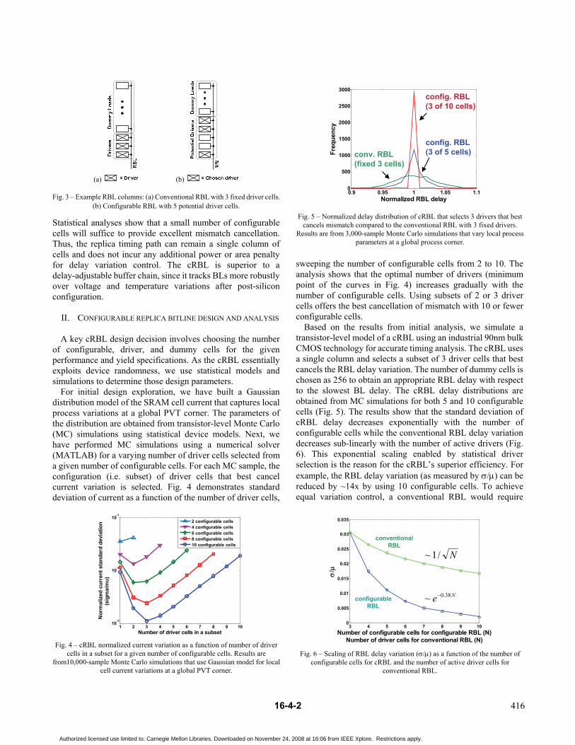
Statistical analyses show that a small number of configurable cells will suffice to provide excellent mismatch cancellation. Thus, the replica timing path can remain a single column of cells and does not incur any additional power or area penalty for delay variation control. The cRBL is superior to a delay-adjustable buffer chain, since it tracks BLs more robustly over voltage and temperature variations after post-silicon configuration.
II. CONFIGURABLE REPLICA BITLINE DESIGN AND ANALYSIS A key cRBL design decision involves choosing the number
of configurable, driver, and dummy cells for the given performance and yield specifications. As the cRBL essentially exploits device randomness, we use statistical models and simulations to determine those design parameters.
For initial design exploration, we have built a Gaussian distribution model of the SRAM cell current that captures local process variations at a global PVT corner. The parameters of the distribution are obtained from transistor-level Monte Carlo (MC) simulations using statistical device models. Next, we have performed MC simulations using a numerical solver (MATLAB) for a varying number of driver cells selected from a given number of configurable cells. For each MC sample, the configuration (i.e. subset) of driver cells that best cancel current variation is selected. Fig. 4 demonstrates standard deviation of current as a function of the number of driver cells,
sweeping the number of configurable cells from 2 to 10. The analysis shows that the optimal number of drivers (minimum point of the curves in Fig. 4) increases gradually with the number of configurable cells. Using subsets of 2 or 3 driver cells offers the best cancellation of mismatch with 10 or fewer configurable cells.
Based on the results from initial analysis, we simulate a transistor-level model of a cRBL using an industrial 90nm bulk CMOS technology for accurate timing analysis. The cRBL uses a single column and selects a subset of 3 driver cells that best cancels the RBL delay variation. The number of dummy cells is chosen as 256 to obtain an appropriate RBL delay with respect to the slowest BL delay. The cRBL delay distributions are obtained from MC simulations for both 5 and 10 configurable cells (Fig. 5). The results show that the standard deviation of cRBL delay decreases exponentially with the number of configurable cells while the conventional RBL delay variation decreases sub-linearly with the number of active drivers (Fig. 6). This exponential scaling enabled by statistical driver selection is the reason for the cRBL’s superior efficiency. For example, the RBL delay variation (as measured by σ/μ) can be reduced by ~14x by using 10 configurable cells. To achieve equal variation control, a conventional RBL would require
(a) (b)
Fig. 3 – Example RBL columns: (a) Conventional RBL with 3 fixed driver cells. (b) Configurable RBL with 5 potential driver cells.
0.9 0.95 1 1.05 1.10
500
1000
1500
2000
2500
3000
Normalized RBL delay
Freq
uenc
y
config. RBL(3 of 10 cells)
config. RBL (3 of 5 cells)conv. RBL
(fixed 3 cells)
Fig. 5 – Normalized delay distribution of cRBL that selects 3 drivers that best cancels mismatch compared to the conventional RBL with 3 fixed drivers.
Results are from 3,000-sample Monte Carlo simulations that vary local process parameters at a global process corner.
3 4 5 6 7 8 9 100
0.005
0.01
0.015
0.02
0.025
0.03
0.035
Number of configurable cells for configurable RBL (N)Number of driver cells for conventional RBL (N)
σ/μ
conventional RBL
N/1~
Ne 38.0~ −configurable RBL
Fig. 6 – Scaling of RBL delay variation (σ/μ) as a function of the number of
configurable cells for cRBL and the number of active driver cells for conventional RBL.
1 2 3 4 5 6 7 8 9 1010
-3
10-2
10-1
Number of driver cells in a subset
Nor
mal
ized
cur
rent
sta
ndar
d de
viat
ion
(sig
ma/
mu)
2 configurable cells4 configurable cells6 configurable cells8 configurable cells10 configurable cells
Fig. 4 – cRBL normalized current variation as a function of number of driver
cells in a subset for a given number of configurable cells. Results are from10,000-sample Monte Carlo simulations that use Gaussian model for local
cell current variations at a global PVT corner.
41616-4-2
Authorized licensed use limited to: Carnegie Mellon Libraries. Downloaded on November 24, 2008 at 16:06 from IEEE Xplore. Restrictions apply.

~600 active driver cells using ~200 columns and thus increase the power and area overhead of the self-timing path by ~200x.
III. CONFIGURABLE REPLICA BITLINE TEST AND
CONFIGURATION Although the cRBL is superior to the conventional RBL, it
relies on post-silicon test and configuration. Therefore, the development of efficient test and configuration techniques is required to make the cRBL practically viable. The primary goal of the cRBL test/configuration is to select a configuration of replica cells that provides the appropriate SAE timing so that the memory can be read correctly at the specified clock speed. For a given cRBL configuration, the tester (either on-chip built-in self-test logic or automated test equipment), which can read and write data from every address in the memory at-speed (e.g. by applying a specific marching pattern [4]), can detect a read failure and thereby can report a pass/fail evaluation. If the tester finds a configuration that evaluates as pass for the whole array, the configuration can be used to control SAE timing during normal memory operation. To avoid failures due to change in environmental conditions, an additional delay margin can be added to the BL path during test to force marginally fast configurations to fail. To further increase read speed and/or reduce bitline power, the above test scheme can be improved to enable speed binning of configurations. Repeating the array read/write tests for varying additional delays on the BL path, configurations can be classified based on their speed at the expense of test time and complexity.
Simulating the proposed post-silicon test/configuration scheme to quantitatively analyze yield recovery enabled by the cRBL necessitates a timing model of the memory that includes the uncertainty of both BL and RBL delays. We have used the same modeling approach as the initial design explorations. SRAM cell currents are modeled as Gaussian random variables and a first-order timing model is used to compute the BL and RBL delays. MC simulations are performed to obtain the statistics of yield recovery enabled by the cRBL. We have applied the analysis technique to a 64kb SRAM prototype. The results given in Table I demonstrate that using cRBLs the parametric yield due to self-timing failures can be increased from ~83% to over 99.99% at a specified clock frequency.
Although the test overhead is not considered in our analysis and a built-in self-test (BIST) engine was not implemented in the test chip, we believe that it would be of a low overhead cost relative to the benefit obtained from cRBLs.
TABLE I
YIELD RECOVERY BY CONFIGURABLE RBL # of configurable cells Self-timing yield 3 (conventional RBL) 83.083% 4 95.686% 6 99.667% 8 99.975% 10 99.998%
Results from 1M-sample MC simulations assuming no memory redundancy. The selection criteria for a
passing configuration is that it should be at least 40ps (~1 F04 inverter delay) slower than the slowest BL
and faster than a specified limit. The resulting SAE timing uncertainty is smaller than ~50ps.
IV. TEST CHIP AND MEASUREMENT RESULTS
To demonstrate the efficacy of the proposed cRBL technique,
a 64kb SRAM prototype has been designed and manufactured in 90nm bulk CMOS (Fig. 7). The implemented cRBL uses a single column with 10 configurable cells and 256 dummy load cells (Fig. 8). A scan chain sets the configurable cell control bits determining which driver cells are used. The test chip is instrumented with on-chip samplers that enable precise read-out of internal node waveforms and accurate measurement of internal delays [5].
Fig. 9 shows the sampled waveforms for internal signals in the bitline and the self-timing paths during a read at 1.0V supply and 100 MHz external clock (CLK). CLK to SAE delay of each cRBL configuration is measured by sampling clock and the SAE signal with 10 ps resolution. Fig. 10 shows the measured CLK to SAE delays from one test chip for conventional RBL mode using 3 fixed driver cells and the cRBL mode using 10 configurable cells. While the conventional RBL provides a fixed delay of 1.68ns, the cRBL provides a delay tunable between 1.66-1.75ns (90ps tuning range). The measurements from 18 test chips show that the tuning range of the cRBL varies between 60-130ps. These results agree closely with the expected tuning range obtained from transistor-level MC simulations (Fig. 11).
We have also processed the measured delay data to emulate a post-silicon configuration step. A cRBL with 10 configurable cells can emulate a cRBL with fewer configurable cells by
Fig. 8 – Circuit schematic of the implemented cRBL.
Fig. 7 – Die photo of the 2mm x 1.2mm test chip with three 64kb SRAM macros one of which is instrumented with on-die samplers in 90nm bulk CMOS.
41716-4-3
Authorized licensed use limited to: Carnegie Mellon Libraries. Downloaded on November 24, 2008 at 16:06 from IEEE Xplore. Restrictions apply.
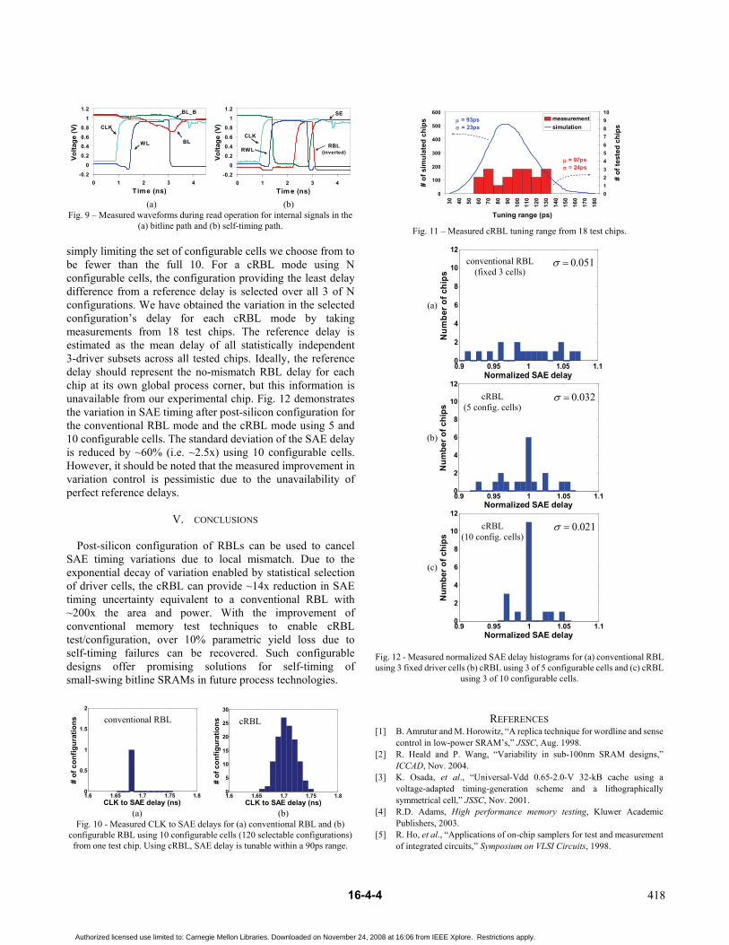
simply limiting the set of configurable cells we choose from to be fewer than the full 10. For a cRBL mode using N configurable cells, the configuration providing the least delay difference from a reference delay is selected over all 3 of N configurations. We have obtained the variation in the selected configuration’s delay for each cRBL mode by taking measurements from 18 test chips. The reference delay is estimated as the mean delay of all statistically independent 3-driver subsets across all tested chips. Ideally, the reference delay should represent the no-mismatch RBL delay for each chip at its own global process corner, but this information is unavailable from our experimental chip. Fig. 12 demonstrates the variation in SAE timing after post-silicon configuration for the conventional RBL mode and the cRBL mode using 5 and 10 configurable cells. The standard deviation of the SAE delay is reduced by ~60% (i.e. ~2.5x) using 10 configurable cells. However, it should be noted that the measured improvement in variation control is pessimistic due to the unavailability of perfect reference delays.
V. CONCLUSIONS
Post-silicon configuration of RBLs can be used to cancel
SAE timing variations due to local mismatch. Due to the exponential decay of variation enabled by statistical selection of driver cells, the cRBL can provide ~14x reduction in SAE timing uncertainty equivalent to a conventional RBL with ~200x the area and power. With the improvement of conventional memory test techniques to enable cRBL test/configuration, over 10% parametric yield loss due to self-timing failures can be recovered. Such configurable designs offer promising solutions for self-timing of small-swing bitline SRAMs in future process technologies.
REFERENCES
[1] B. Amrutur and M. Horowitz, “A replica technique for wordline and sense control in low-power SRAM’s,” JSSC, Aug. 1998.
[2] R. Heald and P. Wang, “Variability in sub-100nm SRAM designs,” ICCAD, Nov. 2004.
[3] K. Osada, et al., “Universal-Vdd 0.65-2.0-V 32-kB cache using a voltage-adapted timing-generation scheme and a lithographically symmetrical cell,” JSSC, Nov. 2001.
[4] R.D. Adams, High performance memory testing, Kluwer Academic Publishers, 2003.
[5] R. Ho, et al., “Applications of on-chip samplers for test and measurement of integrated circuits,” Symposium on VLSI Circuits, 1998.
-0.2
0
0.2
0.40.6
0.8
1
1.2
0 1 2 3 4Time (ns)
Volta
ge (V
) CLK
WL BL
BL_B
-0.2
0
0.2
0.4
0.6
0.8
1
1.2
0 1 2 3 4Tim e (ns)
Volta
ge (V
)
CLK
RWLRBL
(inverted)
SE
(a) (b) Fig. 9 – Measured waveforms during read operation for internal signals in the
(a) bitline path and (b) self-timing path.
0.9 0.95 1 1.05 1.10
2
4
6
8
10
12
Normalized SAE delay
Num
ber o
f chi
ps
0.9 0.95 1 1.05 1.10
2
4
6
8
10
12
Normalized SAE delay
Num
ber o
f chi
ps
0.9 0.95 1 1.05 1.10
2
4
6
8
10
12
Normalized SAE delay
Num
ber o
f chi
ps
Fig. 12 - Measured normalized SAE delay histograms for (a) conventional RBL using 3 fixed driver cells (b) cRBL using 3 of 5 configurable cells and (c) cRBL
using 3 of 10 configurable cells.
1.6 1.65 1.7 1.75 1.80
0.5
1
1.5
2
CLK to SAE delay (ns)
# of
con
figur
atio
ns
1.6 1.65 1.7 1.75 1.80
5
10
15
20
25
30
CLK to SAE delay (ns)
# of
con
figur
atio
ns
(a) (b)
Fig. 10 - Measured CLK to SAE delays for (a) conventional RBL and (b) configurable RBL using 10 configurable cells (120 selectable configurations) from one test chip. Using cRBL, SAE delay is tunable within a 90ps range.
0
100
200
300
400
500
600
30 40 50 60 70 80 90 100
110
120
130
140
150
160
170
180
Tuning range (ps)
# of
sim
ulat
ed c
hips
012345678910
# of
test
ed c
hips
measurementsimulation
μ = 93psσ = 23ps
μ = 97psσ = 24ps
Fig. 11 – Measured cRBL tuning range from 18 test chips.
conventional RBL cRBL
051.0=σconventional RBL (fixed 3 cells)
032.0=σcRBL (5 config. cells)
cRBL (10 config. cells)
021.0=σ
(a)
(b)
(c)
41816-4-4
Authorized licensed use limited to: Carnegie Mellon Libraries. Downloaded on November 24, 2008 at 16:06 from IEEE Xplore. Restrictions apply.