Uttyler ScholarWorks - University of Texas at Tyler
63
University of Texas at Tyler Scholar Works at UT Tyler Electrical Engineering eses Electrical Engineering Fall 2-4-2013 Design of a 2.4 GHz Horizontally Polarized Microstrip Patch Antenna using Rectangular and Circular Directors and Reflectors Yosef Yilak Woldeamanuel Follow this and additional works at: hps://scholarworks.uyler.edu/ee_grad Part of the Electrical and Computer Engineering Commons is esis is brought to you for free and open access by the Electrical Engineering at Scholar Works at UT Tyler. It has been accepted for inclusion in Electrical Engineering eses by an authorized administrator of Scholar Works at UT Tyler. For more information, please contact [email protected]. Recommended Citation Woldeamanuel, Yosef Yilak, "Design of a 2.4 GHz Horizontally Polarized Microstrip Patch Antenna using Rectangular and Circular Directors and Reflectors" (2013). Electrical Engineering eses. Paper 14. hp://hdl.handle.net/10950/104
Transcript of Uttyler ScholarWorks - University of Texas at Tyler
University of Texas at TylerScholar Works at UT Tyler
Electrical Engineering Theses Electrical Engineering
Fall 2-4-2013
Design of a 2.4 GHz Horizontally PolarizedMicrostrip Patch Antenna using Rectangular andCircular Directors and ReflectorsYosef Yilak Woldeamanuel
Follow this and additional works at: https://scholarworks.uttyler.edu/ee_grad
Part of the Electrical and Computer Engineering Commons
This Thesis is brought to you for free and open access by the ElectricalEngineering at Scholar Works at UT Tyler. It has been accepted forinclusion in Electrical Engineering Theses by an authorized administratorof Scholar Works at UT Tyler. For more information, please [email protected].
Recommended CitationWoldeamanuel, Yosef Yilak, "Design of a 2.4 GHz Horizontally Polarized Microstrip Patch Antenna using Rectangular and CircularDirectors and Reflectors" (2013). Electrical Engineering Theses. Paper 14.http://hdl.handle.net/10950/104

DESIGN OF A 2.4GHZ HORIZONTALLY POLARIZED MICROSTRIP
PATCH ANTENNA USING RECTANGULAR AND CIRCULAR
DIRECTORS AND REFLECTORS
by
YOSEF YILAK WOLDEAMANUEL
A thesis submitted in partial fulfillmentof the requirements for the degree of
Master of Science in Electrical EngineeringDepartment of Electrical Engineering
Hector A. Ochoa, Ph.D., Committee ChairCollege of Engineering and Computer Science
The University of Texas at TylerNovember 2012


Acknowledgements
First of all, I would like to give special thanks to my family who has always been
there when I needed with constant support and guidance. You never had a doubt in
your mind and stood behind me from day one. You always listened and felt my pain.
You gave me strength and energy. And you often opened my eyes when I was blind.
Thank you so much for just being there! Love you guys!!!!!
I would like to thank my advisor, Dr. Hector A. Ochoa, for his continuous encourage-
ment, invaluable supervision, timely suggestions and inspired guidance throughout
the completion of this thesis.
I would like to thank Dr. Mukul Shirvaikar for guiding me, advising me and encour-
aging me throughout my Master’s program. I would like to thank my committee
member Dr. Ron J. Pieper for taking time and reviewing my work. I also would like
to thank the entire EE department faculty members for their support and encourage-
ment they gave to me.
Finally, I extend my gratitude to one and all who are directly or indirectly involved
in the successful completion of this thesis work.

Table of Contents
List of Tables . . . . . . . . . . . . . . . . . . . . . . . . . . . . . . . . . . . . iv
List of Figures . . . . . . . . . . . . . . . . . . . . . . . . . . . . . . . . . . . v
Abstract . . . . . . . . . . . . . . . . . . . . . . . . . . . . . . . . . . . . . . . vii
Chapter One: Background . . . . . . . . . . . . . . . . . . . . . . . . . . . . . 1
1.1 Introduction . . . . . . . . . . . . . . . . . . . . . . . . . . . . . . . . 1
1.2 Types of Antennas . . . . . . . . . . . . . . . . . . . . . . . . . . . . 1
1.2.1 Wire Antennas . . . . . . . . . . . . . . . . . . . . . . . . . . 1
1.2.2 Aperture Antennas . . . . . . . . . . . . . . . . . . . . . . . . 2
1.2.3 Microstrip Antennas . . . . . . . . . . . . . . . . . . . . . . . 2
1.2.4 Array Antennas . . . . . . . . . . . . . . . . . . . . . . . . . . 3
1.2.5 Reflector Antennas . . . . . . . . . . . . . . . . . . . . . . . . 4
1.2.6 Lens Antennas . . . . . . . . . . . . . . . . . . . . . . . . . . 4
1.3 Fundamental Parameters of Antenna . . . . . . . . . . . . . . . . . . 5
1.3.1 Radiation Pattern . . . . . . . . . . . . . . . . . . . . . . . . . 5
1.3.2 BeamWidth . . . . . . . . . . . . . . . . . . . . . . . . . . . . 6
1.3.3 Radiation Intensity . . . . . . . . . . . . . . . . . . . . . . . . 7
1.3.4 Directivity . . . . . . . . . . . . . . . . . . . . . . . . . . . . . 8
1.3.5 Antenna Efficiency . . . . . . . . . . . . . . . . . . . . . . . . 8
1.3.6 Antenna Gain . . . . . . . . . . . . . . . . . . . . . . . . . . . 9
i

1.3.7 BandWidth . . . . . . . . . . . . . . . . . . . . . . . . . . . . 9
1.3.8 Polarization . . . . . . . . . . . . . . . . . . . . . . . . . . . . 10
1.3.9 Input Impedance . . . . . . . . . . . . . . . . . . . . . . . . . 10
1.4 Antenna Modeling . . . . . . . . . . . . . . . . . . . . . . . . . . . . 12
1.5 Antenna Simulation Software . . . . . . . . . . . . . . . . . . . . . . 14
Chapter Two: Microstrip Antenna . . . . . . . . . . . . . . . . . . . . . . . . 16
2.1 Introduction . . . . . . . . . . . . . . . . . . . . . . . . . . . . . . . . 16
2.2 Radiation Mechanism of Microstrip Antenna . . . . . . . . . . . . . . 18
2.3 Feeding Techniques and Modeling . . . . . . . . . . . . . . . . . . . . 19
2.4 Microstrip Antenna Design Considerations . . . . . . . . . . . . . . . 20
2.4.1 Substrate Selection . . . . . . . . . . . . . . . . . . . . . . . . 20
2.4.2 Element Width and Length . . . . . . . . . . . . . . . . . . . 21
2.4.3 Radiation Patterns and Radiation Resistance . . . . . . . . . 23
2.4.4 Feed Point Location . . . . . . . . . . . . . . . . . . . . . . . 24
2.4.5 Polarization . . . . . . . . . . . . . . . . . . . . . . . . . . . . 25
Chapter Three: Microstrip Patch Antenna Design and Simulation Results . . 26
3.1 Review of Relevant Works . . . . . . . . . . . . . . . . . . . . . . . . 26
3.2 Microstrip Patch Antenna Design . . . . . . . . . . . . . . . . . . . . 27
3.3 Simulation Results . . . . . . . . . . . . . . . . . . . . . . . . . . . . 29
3.3.1 Radiation Pattern . . . . . . . . . . . . . . . . . . . . . . . . . 29
3.3.2 Antenna Gain . . . . . . . . . . . . . . . . . . . . . . . . . . . 31
3.3.3 Return Loss . . . . . . . . . . . . . . . . . . . . . . . . . . . . 32
3.4 Directors and Reflectors Design . . . . . . . . . . . . . . . . . . . . . 32
3.5 Design 1 : Rectangular Reflector and Four Rectangular Directors . . 34
3.5.1 Radiation Pattern . . . . . . . . . . . . . . . . . . . . . . . . . 35
ii

3.5.2 Antenna Gain . . . . . . . . . . . . . . . . . . . . . . . . . . . 36
3.5.3 Return Loss . . . . . . . . . . . . . . . . . . . . . . . . . . . . 37
3.6 Design 2 : Loop Director and Rectangular Reflector . . . . . . . . . . 41
3.6.1 Radiation Pattern . . . . . . . . . . . . . . . . . . . . . . . . . 42
3.6.2 Antenna Gain . . . . . . . . . . . . . . . . . . . . . . . . . . . 43
3.6.3 Return Loss . . . . . . . . . . . . . . . . . . . . . . . . . . . . 44
Chapter Four: Conclusion and Future Work . . . . . . . . . . . . . . . . . . . 48
4.1 Conclusion . . . . . . . . . . . . . . . . . . . . . . . . . . . . . . . . . 48
4.2 Future Work . . . . . . . . . . . . . . . . . . . . . . . . . . . . . . . . 49
References . . . . . . . . . . . . . . . . . . . . . . . . . . . . . . . . . . . . . . 50
iii

List of Tables
Table 3.1 Antenna Elements Dimensions,Locations, and Substrate Thickness 35
Table 3.2 Antenna Elements Dimensions,Locations, and Substrate Thickness 41
Table 3.3 Antenna Elements Dimensions,Locations, and Substrate Thickness 45
iv

List of Figures
Figure 1.1 Wire antenna configuration . . . . . . . . . . . . . . . . . . . . . 2
Figure 1.2 Aperture antenna configurations . . . . . . . . . . . . . . . . . . . 3
Figure 1.3 Rectangular microstrip patch antenna . . . . . . . . . . . . . . . 3
Figure 1.4 Array configurations(Yagi Uda and Microstrip Array) . . . . . . . 4
Figure 1.5 Reflector antenna configuration . . . . . . . . . . . . . . . . . . . 5
Figure 1.6 Lens antenna configurations . . . . . . . . . . . . . . . . . . . . . 5
Figure 1.7 Coordinate system for antenna analysis . . . . . . . . . . . . . . . 6
Figure 1.8 Radiation lobes and beam widths of an antenna pattern . . . . . 7
Figure 1.9 Polarizations (Linear, Circular, and Elliptical) . . . . . . . . . . . 11
Figure 1.10 Geometry of Yee cell . . . . . . . . . . . . . . . . . . . . . . . . . 14
Figure 2.1 Microstrip patch antenna configuration . . . . . . . . . . . . . . . 17
Figure 2.2 Microstrip antenna charge distribution and current density . . . 18
Figure 2.3 Fringing fields for the dominant mode in a rectangular Microstrip
patch . . . . . . . . . . . . . . . . . . . . . . . . . . . . . . . . . . 19
Figure 2.4 Magnetic and electric wall model of microstrip patch antenna . . 21
Figure 2.5 Two slots model . . . . . . . . . . . . . . . . . . . . . . . . . . . 22
Figure 3.1 Rectangular microstrip patch antenna configuration . . . . . . . . 28
Figure 3.2 2D (phi=0 degrees) cut view of E- field . . . . . . . . . . . . . . . 30
Figure 3.3 3D far zone total E-Field distribution . . . . . . . . . . . . . . . . 30
Figure 3.4 3D far zone E-Field distribution (Theta view) . . . . . . . . . . . 31
v

Figure 3.5 3D far zone E-Field distribution (Phi view) . . . . . . . . . . . . 31
Figure 3.6 2D (phi=0 degrees) cut view of the gain . . . . . . . . . . . . . . 33
Figure 3.7 3D far zone total gain . . . . . . . . . . . . . . . . . . . . . . . . 33
Figure 3.8 Return loss (S11) and steady state parameters . . . . . . . . . . . 34
Figure 3.9 Microstrip antenna configuration with Directors and Reflector . . 35
Figure 3.10 2D (phi=0 degrees) cut view of E- field . . . . . . . . . . . . . . . 36
Figure 3.11 3D far zone total E-Field distribution . . . . . . . . . . . . . . . . 36
Figure 3.12 Radiation pattern variation with director positions . . . . . . . . 37
Figure 3.13 2D (phi=0 degrees) cut view of the gain . . . . . . . . . . . . . . 38
Figure 3.14 3D far zone total gain . . . . . . . . . . . . . . . . . . . . . . . . 38
Figure 3.15 Return loss (S11) and steady state parameters . . . . . . . . . . 39
Figure 3.16 Microstrip patch antenna configuration with directors and reflector 39
Figure 3.17 3D far zone total gain . . . . . . . . . . . . . . . . . . . . . . . . 40
Figure 3.18 Microstrip patch antenna configuration with loop director . . . . 41
Figure 3.19 2D (phi=0 degrees) cut view of E- field . . . . . . . . . . . . . . . 42
Figure 3.20 3D far zone total E-Field distribution . . . . . . . . . . . . . . . . 42
Figure 3.21 2D (phi=0 degrees) cut view of the gain . . . . . . . . . . . . . . 43
Figure 3.22 3D far zone total gain . . . . . . . . . . . . . . . . . . . . . . . . 43
Figure 3.23 Return loss (S11) and steady state parameters . . . . . . . . . . . 44
Figure 3.24 Microstrip antenna configuration with three reflectors . . . . . . . 45
Figure 3.25 2D (phi=0 degrees) cut view of the gain . . . . . . . . . . . . . . 46
Figure 3.26 3D far zone total gain . . . . . . . . . . . . . . . . . . . . . . . . 46
Figure 3.27 Return loss (S11) and steady state parameters . . . . . . . . . . . 47
vi

Abstract
DESIGN OF A 2.4GHZ HORIZONTALLY POLARIZED MICROSTRIPPATCH ANTENNA USING RECTANGULAR AND CIRCULAR
DIRECTORS AND REFLECTORS
YOSEF YILAK WOLDEAMANUEL
Thesis Chair: Hector A. Ochoa, Ph.D.
The University of Texas at Tyler
November 2012
In the urban or indoor wireless environment, after a complicated multiple reflection
or scattering effect, the polarization of the propagating radio wave may change signif-
icantly. Although many current wireless systems are vertically polarized, it has been
predicted that it is advantageous to use horizontally polarized antennas at both the
transmitter and receiver ends. A horizontally polarized antenna is less likely to pick
up man-made interference produced by automobile ignition systems and electrical
appliances, which is usually vertically polarized. A second advantage is that there
is less absorption of radiated energy by buildings or wiring when these antennas are
used. Another advantage is that support structures for these antennas are of a more
convenient size than those for vertically polarized antennas. Finally, horizontally po-
larized waves suffer lower losses than vertically polarized waves, especially above 100
MHz.
Modern communication systems and instruments such as Wireless Local Area Net-
works (WLAN), mobile handsets and local positioning systems (LPS) require lightweight,
small size and low cost antennas. The selection of microstrip antenna technology can
fulfill these requirements. The main problem is that they usually radiate in a direc-
tion along the ground plane (vertically), and the gain in the horizontal direction is
vii

only a few decibels.
In this thesis, new designs are proposed to develop a horizontally polarized microstrip
patch antennas for 2.4 GHz applications using directors and reflectors to guide the
radiated power. This thesis will focus on the development of designs which retain the
advantages of microstrip patch antenna while improving its horizontal radiation. The
results from the two most significant antenna configurations are discussed and ana-
lyzed. The first design is composed of four rectangular directors and one rectangular
reflector. The second design is composed of one loop director and one rectangu-
lar reflector. The radiation characteristics of these designs with respect to various
geometrical parameters such as the dimensions of the reflector and directors, and
spacing between these elements are studied in order to obtain the best possible per-
formance. Furthermore, two-dimensional and three-dimensional radiation patterns,
antenna gain and return loss for each of these designs are presented.
The results from the first design yielded a radiation pattern with an elevation of
20 degrees with a maximum gain of 2.033 dBi. The proposed antenna structure has
dimensions of 61.785mm x 67.65 mm, and a total height of 35.794mm. The results
from the second design yielded a radiation pattern with an elevation of 0 degrees with
a maximum gain of 3.847 dBi. The compactness of the overall antenna structure was
further improved to 61.875mm x 67.65mm, and a total height of 30.794mm. The
input impedance and resonance center frequencies are also in the desired range for
both designs. The proposed compact antennas present an excellent candidate for the
emerging wireless communications with large amount of data transmitting in rapid
bursts requirement at 2.4 GHz frequency, which include Bluetooth and WiFi (802.11).
viii

Chapter One
Background
1.1 Introduction
An antenna is a device used to transform an RF signal, traveling on a conductor, into
an electromagnetic guided wave in free space, and vice versa (i.e., in either trans-
mitting or receiving mode of operation). Antennas are frequency-dependent devices.
Each antenna is designed for a certain frequency band, and it rejects signals beyond
the operating band. For that reason, antennas can be considered bandpass filters and
transducers. In addition, an antenna in advanced wireless systems is usually required
to optimize or accentuate the radiation energy in some directions and suppress it in
others. Nowadays, these devices constitute an essential part of wireless communica-
tion systems [1].
Basic antenna classification depends on design particularities, mode of operations
and their applications. The isotropic point source radiator, which radiates the same
intensity of electromagnetic signal in all directions, is considered as a benchmark for
other antennas. However, these sources do not exist, but most antennas’ gains are
measured with respect to this specific radiator.
1.2 Types of Antennas
1.2.1 Wire Antennas
Wire antennas are a simple and familiar type of antenna, which are seen almost
everywhere - on automobiles, buildings, ships, and aircraft. There are various shapes
of wire antennas such as a straight wire (dipole), loop, and helix. In the case of loop
antennas, they are not required to possess a circular shape. They can take the form
of a rectangle, square, ellipse, or any other desired shape. However, the circular loop
1

is the most common configuration, because of its simplicity in construction. The
configuration of the dipole and circular loop antenna is shown in figure 1.1.
Figure 1.1: Wire antenna configuration
1.2.2 Aperture Antennas
The use of aperture antennas is becoming more and more typical. An aperture an-
tenna contains some sort of opening through which electromagnetic waves are trans-
mitted or received. Examples of aperture antennas include slots, waveguides, and
horn antennas. Three different configurations of horn antennas (pyramidal, conical,
and rectangular) are shown in the figure 1.2. Antennas of this type are very useful in
space missions, because they can be used to produce wide-beam coverage and can be
conveniently flush-mounted onto the skin of the aircraft or spacecraft. In addition,
they can be covered with a dielectric material to protect them from hazardous con-
ditions.
1.2.3 Microstrip Antennas
Microstrip antennas became very popular in the 1970s primarily for spaceborne ap-
plications. Today, they are heavily used for government and commercial applications.
These antennas consist of a metallic patch on a grounded substrate. A graphical rep-
resentation of a microstrip patch antenna is shown in figure 1.3. The metallic patch
2

Figure 1.2: Aperture antenna configurations
on the top of the substrate can take different configurations. However, the rectangular
and circular patches are the most popular, because they are easy to analyze and fab-
ricate, and their attractive radiation characteristics, especially low cross-polarization
radiation. Microstrip antennas have low profile, and they are simple and inexpen-
sive to fabricate using modern printed-circuit technology. They are also mechanically
robust when mounted on rigid surfaces, and compatible with Monolithic Microwave
Integrated Circuit (MMIC) designs. Microstrip antennas are versatile in terms of
resonant frequency, polarization, radiation pattern, and impedance. These antennas
can be mounted on the surface of high-performance aircraft, spacecraft, satellites,
missiles, cars, and even handheld mobile devices [2].
Figure 1.3: Rectangular microstrip patch antenna
1.2.4 Array Antennas
Many applications require radiation patterns and gains that may not be achieved
by a single element antenna. In order to obtain the desired radiation characteristics
3

several single antenna elements are combined to form an antenna array. Examples of
a microstrip patch array and a Yagi - Uda array are shown in figure 1.4. The arrange-
ment of the array is in such a way that the radiation from each individual element
adds up to produce a maximum radiation in a particular direction or directions. The
overall radiation characteristics of array antennas can be influenced by the number of
elements, spacing, and radiating element properties. Unlike a single element antenna
whose radiation pattern is fixed, the radiation pattern of array antennas, called the
array pattern, can be changed upon exciting its elements with different currents. This
provides a freedom to design a certain desired array pattern from an array without
changing its physical dimensions [3].
Figure 1.4: Array configurations(Yagi Uda and Microstrip Array)
1.2.5 Reflector Antennas
Reflector antennas are high gain antennas, which can easily achieve gains above 30
dB for microwave and higher frequencies. They are used for long distance radio
communication, high-resolution radars, and radio-astronomy. A typical example of a
reflector antenna configuration is the parabolic reflector shown in figure 1.5. Antennas
of this type have been built with diameters as large as 305 m [4].
1.2.6 Lens Antennas
Lenses are primarily used to collimate incident divergent energy to prevent it from
spreading in undesired directions. By properly shaping the geometrical configuration
and choosing the appropriate material of the lenses, they can transform various forms
4
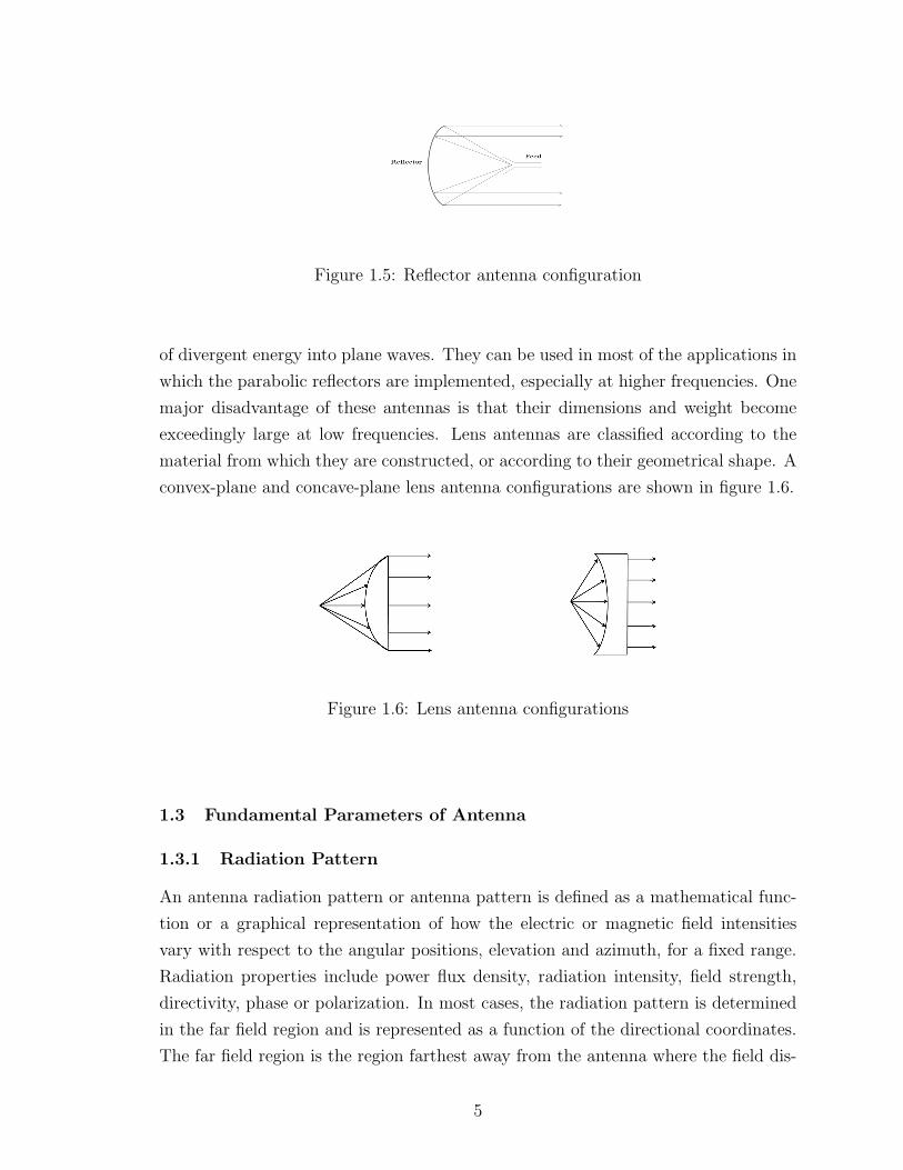
Figure 1.5: Reflector antenna configuration
of divergent energy into plane waves. They can be used in most of the applications in
which the parabolic reflectors are implemented, especially at higher frequencies. One
major disadvantage of these antennas is that their dimensions and weight become
exceedingly large at low frequencies. Lens antennas are classified according to the
material from which they are constructed, or according to their geometrical shape. A
convex-plane and concave-plane lens antenna configurations are shown in figure 1.6.
Figure 1.6: Lens antenna configurations
1.3 Fundamental Parameters of Antenna
1.3.1 Radiation Pattern
An antenna radiation pattern or antenna pattern is defined as a mathematical func-
tion or a graphical representation of how the electric or magnetic field intensities
vary with respect to the angular positions, elevation and azimuth, for a fixed range.
Radiation properties include power flux density, radiation intensity, field strength,
directivity, phase or polarization. In most cases, the radiation pattern is determined
in the far field region and is represented as a function of the directional coordinates.
The far field region is the region farthest away from the antenna where the field dis-
5

tribution is independent of the distance from the antenna. It is identified by those
distances greater than 2D2/λo, D being the maximum overall dimension of the an-
tenna and λo the free-space wavelength [5].
In general, most of the radiation patterns are composed of multiple lobes, which may
Figure 1.7: Coordinate system for antenna analysis
be sub classified into major or main, minor, side, and back lobes as shown in figure
1.7. A radiation lobe is a portion of the radiation pattern bounded by regions of rel-
atively weak radiation intensity. A major lobe (also called main beam) is defined as
the radiation lobe containing the direction of maximum radiation. In some antennas,
such as split-beam antennas, there may exist more than one major lobe. A sidelobe
is a radiation lobe in any direction other than the intended lobe. Usually a sidelobe
is adjacent to the main lobe and occupies the hemisphere in the direction of the main
beam. A backlobe is a radiation lobe whose axis makes an angle of approximately
1800 with respect to the beam of an antenna. Usually it refers to a minor lobe that
occupies the hemisphere in a direction opposite to that of the major (main) lobe [1].
1.3.2 BeamWidth
The beamwidth of an antenna is defined as the angular separation between two iden-
tical points on opposite sides of the pattern maximum. In an antenna pattern, there
are a number of beamwidths as indicted in figure 1.8. One of the most widely used
beamwidth is the Half-Power Beamwidth (HPBW), which is defined by IEEE as,
”In a plane containing the direction of the maximum of a beam, the angle between
6

the two directions in which the radiation intensity is one-half value of the beam”
[4]. Another important beamwidth is the angular separation between the first nulls
of the pattern, and it is referred to as the First-Null Beam width (FNBW). Other
beamwidths are those where the pattern is -10 dB from the maximum, or any other
value. However, in practice, the term beamwidth, with no other identification, usu-
ally refers to HPBW [1]. The beamwidth of an antenna is an important parameter,
and often is used to describe the resolution capabilities of the antenna to distinguish
between two adjacent radiating sources or radar targets.
Figure 1.8: Radiation lobes and beam widths of an antenna pattern
1.3.3 Radiation Intensity
Radiation intensity in a given direction is defined as the power radiated from an an-
tenna per unit solid angle. The radiation intensity is a far-field parameter, and it can
be obtained by multiplying the radiation density by the square of the distance. In a
mathematical form, it is expressed as
U = r2Wrad (1.1)
Where
U - radiation intensity (W/unit solid angle)
7
Wrad - radiation density (W/m2)
r - distance (m)
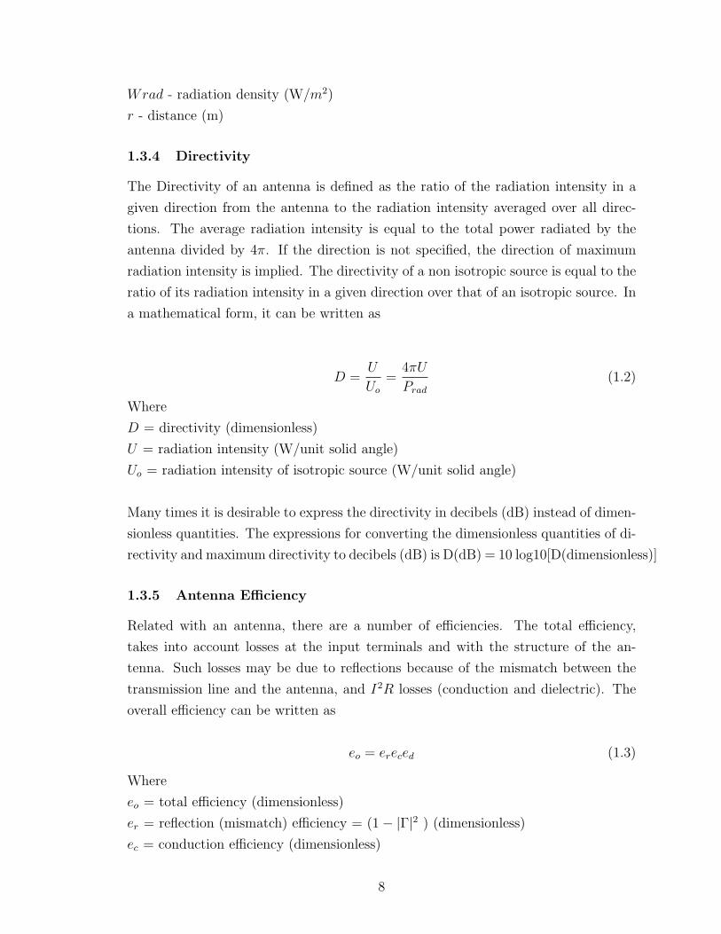
1.3.4 Directivity
The Directivity of an antenna is defined as the ratio of the radiation intensity in a
given direction from the antenna to the radiation intensity averaged over all direc-
tions. The average radiation intensity is equal to the total power radiated by the
antenna divided by 4π. If the direction is not specified, the direction of maximum
radiation intensity is implied. The directivity of a non isotropic source is equal to the
ratio of its radiation intensity in a given direction over that of an isotropic source. In
a mathematical form, it can be written as
D =U
Uo
=4πU
Prad
(1.2)
Where
D = directivity (dimensionless)
U = radiation intensity (W/unit solid angle)
Uo = radiation intensity of isotropic source (W/unit solid angle)
Many times it is desirable to express the directivity in decibels (dB) instead of dimen-
sionless quantities. The expressions for converting the dimensionless quantities of di-
rectivity and maximum directivity to decibels (dB) is D(dB) = 10 log10[D(dimensionless)]
1.3.5 Antenna Efficiency
Related with an antenna, there are a number of efficiencies. The total efficiency,
takes into account losses at the input terminals and with the structure of the an-
tenna. Such losses may be due to reflections because of the mismatch between the
transmission line and the antenna, and I2R losses (conduction and dielectric). The
overall efficiency can be written as
eo = ereced (1.3)
Where
eo = total efficiency (dimensionless)
er = reflection (mismatch) efficiency = (1− |Γ|2 ) (dimensionless)
ec = conduction efficiency (dimensionless)
8

ed = dielectric efficiency (dimensionless)
Γ= voltage reflection coefficient at the input terminals of the antenna
Γ= (Zin −Zo)/(Zin +Zo) where Zin = antenna input impedance,Zo = characteristic
impedance of the transmission line.
V SWR = V oltageStandingWaveRatio =1 + |Γ|1− |Γ|
(1.4)
1.3.6 Antenna Gain
Another useful measure describing the performance of an antenna is the gain. Al-
though the gain of the antenna is closely related to the directivity, it is a measure that
takes into account the efficiency of the antenna as well as its directional capabilities.
It is defined as the ratio of the intensity, in a given direction, to the radiation intensity
that would be obtained if the power accepted by the antenna were radiated isotrop-
ically. The radiation intensity corresponding to the isotropically radiated power is
equal to the power accepted (input) by the antenna divided by 4π
Gain = 4πRadiationIntensity
TotalPower= 4π
U(θ, ϕ)
Pin
(1.5)
In most cases, the gain is relative, which is defined as the ratio of the power gain in
a given direction to the power gain of a reference antenna in its referenced direction.
The reference antenna is usually a dipole or isotropic antenna [6].
1.3.7 BandWidth
The bandwidth of an antenna is defined as the range of frequencies within which the
performance of the antenna, with respect to some characteristic, conforms to a spec-
ified standard. The bandwidth can be considered to be the range of frequencies, on
either side of a center frequency, usually the resonance frequency. In this range, the
antenna characteristics such as input impedance, pattern, beamwidth, polarization,
side lobe level, gain, and radiation efficiency are within an acceptable value of those
at the center frequency. For broadband antennas, the bandwidth is usually expressed
as the ratio of the upper-to-lower frequencies of acceptable operation. For example, a
10:1 bandwidth indicates the upper frequency is 10 times greater than the lower. For
narrowband antennas, the bandwidth is expressed as a percentage of the frequency
9
difference (upper minus lower) over the center frequency of the bandwidth. For ex-
ample, a 5 percent bandwidth indicates that the frequency difference of acceptable
operation is 5 percent of the center frequency of the bandwidth [1].
1.3.8 Polarization
Polarization of a radiated wave is defined as the property of an electromagnetic wave
describing the time-varying direction and relative magnitude of the electric-field vec-
tor. It is described by the geometric figure traced by the electric field vector upon
a stationary plane perpendicular to the direction of propagation, as the wave travels
through that plane. The three different types of antenna polarizations are shown in
figure 1.9. Vertical, and horizontal polarizations are the simplest forms of antenna
polarization and they both fall into a category known as linear polarization. It is also
possible that antennas can have a circular polarization. Circular polarization occurs
when two or more linearly polarized waves add together, such that the E-field of the
net wave rotates. Circular polarization has a number of benefits for areas such as
satellite applications where it helps overcome the effects of propagation anomalies,
ground reflections and the effects of the spin that occur on many satellites [7]. An-
other form of polarization is known as elliptical polarization. It occurs when there
is a mix of linear and circular polarization. This can be visualized by the tip of
the electric field vector tracing out an elliptically shaped corkscrew. It is possible
for linearly polarized antennas to receive circularly polarized signals and vice versa.
But, there is a 3 dB polarization mismatch between linearly and circularly polarized
antennas [8].
1.3.9 Input Impedance
Antenna impedance is presented as the ratio of voltage to current at the antenna’s
terminals. In order to achieve maximum energy transfer the input impedance of the
antenna must identically match the characteristic impedance of the transmission line.
If the two impedances do not match, a reflected wave will be generated at the antenna
terminal and travel back towards the energy source. This reflection of energy results
in a reduction in the overall antenna efficiency. The impedance of an antenna, with
no load attached, is defined as:
10

Figure 1.9: Polarizations (Linear, Circular, and Elliptical)
ZA = RA + jXA (1.6)
Where
ZA = antenna impedance (ohms)
RA = antenna resistance (ohms)
XA = antenna reactance (ohms)
The resistive part
RA = Rr +RL (1.7)
Where
Rr = radiation resistance of the antenna
RL = loss resistance of the antenna
The input impedance of an antenna is generally a function of frequency. Thus, the
antenna will be matched to the interconnecting transmission line and other associ-
ated equipment only within a bandwidth. In addition, the input impedance of the
antenna depends on many factors including its geometry, its method of excitation,
and its proximity to surrounding objects. Because of their complex geometries, only
a limited number of practical antennas had been investigated analytically. For many
others, the input impedance has been determined experimentally.
11
1.4 Antenna Modeling
Maxwell’s partial differential equations of electrodynamics were formulated around
1870. It has been considered as the most outstanding achievement of the 19th-
century science. Maxwell’s equations represent a fundamental unification of electric
and magnetic fields predicting electromagnetic wave phenomena. The solution of
Maxwell’s equations is an area of significant importance to the microwave and antenna
engineering community [4].
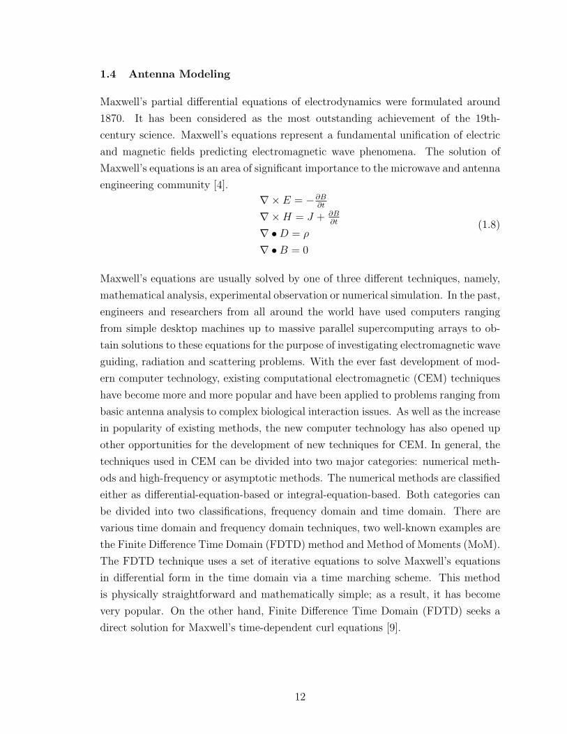
∇× E = −∂B∂t
∇×H = J + ∂B∂t
∇ •D = ρ
∇ • B = 0
(1.8)
Maxwell’s equations are usually solved by one of three different techniques, namely,
mathematical analysis, experimental observation or numerical simulation. In the past,
engineers and researchers from all around the world have used computers ranging
from simple desktop machines up to massive parallel supercomputing arrays to ob-
tain solutions to these equations for the purpose of investigating electromagnetic wave
guiding, radiation and scattering problems. With the ever fast development of mod-
ern computer technology, existing computational electromagnetic (CEM) techniques
have become more and more popular and have been applied to problems ranging from
basic antenna analysis to complex biological interaction issues. As well as the increase
in popularity of existing methods, the new computer technology has also opened up
other opportunities for the development of new techniques for CEM. In general, the
techniques used in CEM can be divided into two major categories: numerical meth-
ods and high-frequency or asymptotic methods. The numerical methods are classified
either as differential-equation-based or integral-equation-based. Both categories can
be divided into two classifications, frequency domain and time domain. There are
various time domain and frequency domain techniques, two well-known examples are
the Finite Difference Time Domain (FDTD) method and Method of Moments (MoM).
The FDTD technique uses a set of iterative equations to solve Maxwell’s equations
in differential form in the time domain via a time marching scheme. This method
is physically straightforward and mathematically simple; as a result, it has become
very popular. On the other hand, Finite Difference Time Domain (FDTD) seeks a
direct solution for Maxwell’s time-dependent curl equations [9].
12

σ−→E + ε∂
−→E∂t
= ∇×−→H
µ∂−→H∂t
= −∇×−→E
(1.9)
Instead of employing potentials to find solution for the Maxwell curl equations, The
FDTD is based upon volumetric sampling of the unknown near field distribution
within and surrounding the structure of interest over a finite period of time. In this
approach, the space is divided into discrete cells, which should be small compared to
the wavelength. The electric fields are located on the edges of the box, and the mag-
netic fields are positioned on the faces as shown in figure 1.10. This orientation of the
fields is known as the Yee cell and is the basis for FDTD [9]. Time is quantized into
small steps where each step represents the time required for the field to travel from
one cell to the next. The electric and magnetic fields are updated using a leapfrog
scheme where first the electric fields, then the magnetic are computed at each step
in time. When many FDTD cells are combined together to form a three-dimensional
volume, the result is an FDTD grid or mesh. Each FDTD cell will overlap edges and
faces with its neighbors, by convention each cell will have three electric fields that
begin at a common node associated with it. The electric fields at the other nine edges
of the FDTD cell will belong to other adjacent cells. Each cell will also have three
magnetic fields originating on the faces of the cell adjacent to the common node of
the electric fields [2].
The FDTD is a general method since it aims at solving Maxwell’s partial differential
equations directly without analytical preprocessing and modeling. Therefore, com-
plex antennas can also be analyzed using this technique. Some of the advantages of
the FDTD techniques are:
• From a mathematical point of view it is a direct implementation of Maxwell’s
curl equations.Therefore, analytical processing of Maxell’s equations is almost
negligible.
• It is capable of predicting broadband frequency response because, the analysis
is carried out in the time domain.
• It is capable of analyzing complex systems, including wave interaction with
human body, or satellite, nonlinear device simulation, and complex antennas.
13

Figure 1.10: Geometry of Yee cell
• It is capable of analyzing structures using different types of materials, for ex-
ample, lossy dielectrics, magnetized ferrites, and anisotropic plasmas.
• It provides a real-time animation display, which is a powerful tool for both a
student and an electromagnetic designer [2].
1.5 Antenna Simulation Software
Although many techniques for accurately simulating the electromagnetic character-
istics of antennas exist, it is difficult to design a good antenna system. Antennas
are frequently designed through an ad-hoc combination of experience, intuition, and
guesswork [7]. Designing antennas for multiple frequency ranges and diverse ap-
plications is even more complicated. There exists a need for new technologies and
methodologies to supplement traditional antenna design techniques. Electromagnetic
Professional (EMPro), is Agilent EEsof EDA’s EM simulation software design plat-
form for analyzing 3D electromagnetic (EM) effects of components such as high-speed
and RF IC packages, bondwires, antennas, on-chip and off-chip embedded passives
and PCB interconnects. EMPro EM simulation software features a modern design,
simulation and analysis environment, high capacity simulation technologies and in-
14

tegration with the industry’s leading RF and microwave circuit design environment,
Advanced Design System (ADS) for fast and efficient RF and microwave circuit de-
sign.
Key Benefits of EMPro EM Simulation Software
• Design Flow Integration: Create 3D components that can be simulated together
with 2D circuit layouts and schematics within Advanced Design System (ADS),
using EM-circuit cosimulation.
• Broad Simulation Technology: Set up and run analyses using both frequency-
domain and time-domain 3D EM simulation technologies: Finite Element Method
(FEM) and Finite Difference Time Domain (FDTD).
• Efficient User Interface: Quickly create arbitrary 3D structures with a mod-
ern, simple GUI that saves time and EMPro EM simulation software provides
advanced scripting features [10].
15

Chapter Two
Microstrip Antenna
2.1 Introduction
The concept of Microstrip radiators was first proposed by Georges A. Deschamps in
1953. However, 20 years passed before practical antennas were actually fabricated.
The development of these antennas during the 1970s was accelerated by the availabil-
ity of good substrate with low loss tangent and attractive thermal and mechanical
properties. Also, the improvement in photolithographic techniques and the availabil-
ity of suitable theoretical models helped the fast development of these antennas. The
first practical antennas were developed by Howell and Munson in the early 1970’s
[2]. Microstrip antennas have considerably matured in the last 25 years, and many
of their limitations have been overcome.
Microstrip antennas are low profile, light weight, inexpensive and easy to integrate
with accompanying electronics antennas. They are most suitable for aerospace and
mobile applications. Many of the antenna applications for satellite links, mobile
communications, and wireless local-area networks, impose constraints on compact-
ness, dual frequency operation, frequency agility, polarization control, and radiation
control. These functions can be achieved by properly loading a simple Microstrip
antenna. For that reason, they are becoming more and more popular [6]. The char-
acteristics of microstrip antennas can be significantly improved by using multilayered
structures with thick substrate and low permittivity materials. Because of their low
power handling capabilities, these antennas can also be used in low power transmit-
ting and receiving applications.
As shown in figure 2.1, a Microstrip antenna in its simplest configuration consists
of a radiating patch on one side of a dielectric substrate which has a ground plane on
the other side. The patch conductors normally made of copper or gold, can assume
16

virtually any shape, but regular shapes, such as rectangles and circles, are generally
used to simplify performance prediction. Ideally, the dielectric constant εr, of the
substrate should be low (εr < 2.5), to enhance the fringing fields that account for
radiation [2].
Figure 2.1: Microstrip patch antenna configuration
Microstrip antennas have several advantages compared to conventional antennas.
Many applications that cover a frequency range of 100 MHz to 100GHz use these
structures. Some of the principal advantages of Microstrip antennas are:
• Light weight, low volume, and thin profile configuration;
• Low fabrication cost;
• Linear and circular polarizations are possible with simple feed;
• Dual frequency and dual polarization antennas can be easily made;
• Can be easily integrated with microwave integrated circuits;
• Feed lines and matching networks can be fabricated with antenna structures.
However, Microstrip antennas also have some limitations compared to conventional
antennas:
17

• Narrow bandwidth and tolerance problems;
• Somewhat lower gain;
• Large ohmic loss in the feed structures and arrays;
• Complex feed structures are required for high performance arrays;
• High cross polarizations and mutual coupling at high frequencies.
2.2 Radiation Mechanism of Microstrip Antenna
The important characteristic of Microstrip antennas is their inherent ability to radiate
efficiently despite their low profile. The primary source of radiation is the electric
fringing fields between the edges of the conductor element and the ground plane.
Thick substrates with low permittivity are used in Microstrip antennas for better
radiation efficiency [11]. The radiation from Microstrip antenna can be determined
from the field distribution between the patch metallization and the ground plane.
Alternatively, radiation can be described in terms of the surface current distribution.
An accurate calculation of the field or current distribution of the patch antenna is
complicated. However, crude approximations and simple arguments can be used to
develop a workable model for Microstrip antennas. A patch, which is connected to
a microwave source, has a charge distribution on the upper and lower surface of the
patch as well as the ground plane as shown in figure 2.2. The excitation of the patch
results in positive and negative charge distribution, mainly because the patch is half
wavelength in the dominant mode [12].
Figure 2.2: Microstrip antenna charge distribution and current density
The repulsive nature of those charges at the bottom surface of the patch pushes some
18

charges around the side to the top generating the current densities Jb and Js. In
microstrip antennas, the height to width ratio (h/W) is small as compared to the
overall patch length. Therefore, the strong attractive forces between the charges
cause that most of the current and charge concentration remains underneath the
patch. However, also the repulsive force between positive charges creates a large
charge density around the edges. The fringing fields generated by these charges are
responsible for the radiation. Figure 2.3 shows the fringing fields in a Microstrip
patch.
Figure 2.3: Fringing fields for the dominant mode in a rectangular Microstrip patch
2.3 Feeding Techniques and Modeling
Microstrip antennas have radiating elements on one side of the dielectric substrate.
Thus, early microstrip antennas were fed either by a microstrip-line or a coaxial
probe through the ground plane. The selection of feeding techniques is governed by
a number of factors. The most important consideration is the efficient power transfer
between the radiating structure and the feed structure, that is, impedance matching
between the radiating and the feed structures. Microstrip patch antennas can be
fed by a variety of methods. These methods can be classified into two categories-
19

contacting and non-contacting. In the contacting method, the RF power is fed di-
rectly to the radiating patch using a connecting element such as a microstrip-line. In
the non-contacting scheme, electromagnetic field coupling is done to transfer power
between the microstrip-line and the radiating patch. The four most popular feeding
techniques are the microstrip-line, coaxial probe (both contacting schemes), aperture
coupling and proximity coupling (both non-contacting schemes). Excitation of mi-
crostrip antennas by a microstrip-line on the same substrate appears to be a natural
choice, because the patch can be considered an extension of the microstrip-line, and
both can be fabricated simultaneously.
The simple transmission line model, the generalized transmission line model, and
the cavity model are some of the techniques used to analyze patch antennas. These
models are used to predict the characteristics of a microstrip patch antenna. These
include its resonant frequency, bandwidth, radiation pattern, etc. The cavity model
becomes a natural choice to analyze microstrip antennas due to the fact that mi-
crostrip patch antennas are narrow-band resonant antennas, which can be termed
lossy cavities. In this model, the interior region of the patch is modeled as a cavity
bounded by electric walls on the top and bottom, and a magnetic wall all along the
periphery. The bases for this assumption are,
• The fields in the interior region do not vary with z (that is, ∂/∂z ≡ 0 ), because
the substrate is very thin, (h<< λo).
• The electric field is radiated only in the z-direction, and the magnetic field has
only the transverse components in the region bounded by the patch metalliza-
tion and the ground plane.
• The electric current in the patch has no component normal to the edge of
the patch metallization, which implies that the tangential component(y and z
directions) of H along the edge is negligible, and a magnetic wall can be placed
along the periphery ( ∂Ez/∂n ≡ 0 ).
2.4 Microstrip Antenna Design Considerations
2.4.1 Substrate Selection
It is critical for the design of these antennas to select a suitable dielectric substrate
of appropriate thickness h, and loss tangent. A thicker substrate, besides being me-
20

Figure 2.4: Magnetic and electric wall model of microstrip patch antenna
chanically strong, will increase the radiated power, reduce conductor loss and improve
impedance bandwidth. However, it will also increase the weight, dielectric loss, sur-
face wave loss and extraneous radiation from the probe feed. A rectangular patch
antenna stops resonating for a substrate thickness greater than 0.11λo due to induc-
tive reactance of the feed. The substrate dielectric constant (εr) plays a role similar
to that of substrate thickness. A low dielectric constant for the substrate will in-
crease the fringing field at the patch periphery. As a result, the radiated power of
the antenna will be also increased. Therefore, a dielectric constant of less than 2.55
(εr <2.55) is preferred unless a smaller patch size is desired. An increase in the sub-
strate thickness has similar effects on the antenna characteristics as decreasing the
value of the dielectric constant . A high substrate loss tangent increases the dielectric
loss of the antenna and reduces the antenna efficiency. The most commonly used
substrate materials are honeycomb ( εr=1.07), duroid (εr=2.32), Quartz (εr=3.8),
and alumina (εr=10).
2.4.2 Element Width and Length
Patch width has a minor effect on the resonant frequency and radiation pattern of the
antenna. However, it affects the input resistance and bandwidth to a larger extent. A
bigger patch width increases the power radiated and thus provides a decreased reso-
nant resistance, increased bandwidth, and increased radiation efficiency. A constraint
against a larger patch width is the generation of grating lobes in antenna arrays. It
has been suggested that the length to width ratio of the path has to lie in the range of
one and two (1 < L/W < 2) to obtain a good radiation efficiency. The patch length
21

determines the resonant frequency, and is a critical parameter in the design, because
of the inherent narrow bandwidth of the patch. The microstrip patch length (L), for
TM10 (Traverse Magnetic) mode of operation can be approximated as;
L =c
2fr√εr
(2.1)
Where
c - Speed of light in free space
fr - Resonant frequency
εr- Dielectric constant of the substrate
In practice, the fields are not confined to the patch. A fraction of the fields lie
outside the physical dimensions of the patch (LxW ) as shown in figure 2.5. This is
called the fringing field.
Figure 2.5: Two slots model
The effect of the fringing field along the patch width, W can be included through
the effective dielectric constant εeff for a Microstrip line of width W on the given
substrate [13].
εeff =εr + 1
2+
εr − 1
2(1 + 12
h
W)−
12 (2.2)
Where
22

εeff = Effective dielectric constant
εr = Dielectric constant of substrate
h = Height of dielectric substrate
W = Width of the patch
Whereas the effect of the fringing field along the patch length L can be described
in terms of an additional line length on either ends of the patch length.
∆L =0.41h(εeff + 0.3)(W
h) + 0.264)
(εeff − 0.258)(Wh+ 08)
(2.3)
The effective length is given by:
Leff = L+ 2L (2.4)
The resonant frequency is:
fr =c
2Leff√εeff
(2.5)
2.4.3 Radiation Patterns and Radiation Resistance
The radiation patterns of microstrip antennas are of prime importance in determining
most of its radiation characteristics, which include beam-width, beam shape, side-
lobe level, directivity, polarization and radiated power. Radiation from a patch can
be derived either from the Ez field across the aperture between the patch and the
ground plane (using vector eclectic potential) or from the currents on the surface of
the patch conductor (employing vector magnetic potentials). The two-slot model and
electric surface current model are commonly used to calculate the radiation patterns
of microstrip antennas. In the first case, the antenna is modeled as a combination of
two parallel slots of length W , width h, and spaced a distance L apart, whereas in the
second case, the patch metallization is replaced by the surface current distribution.
The radiation patterns obtained from the two different approaches are very similar.
23
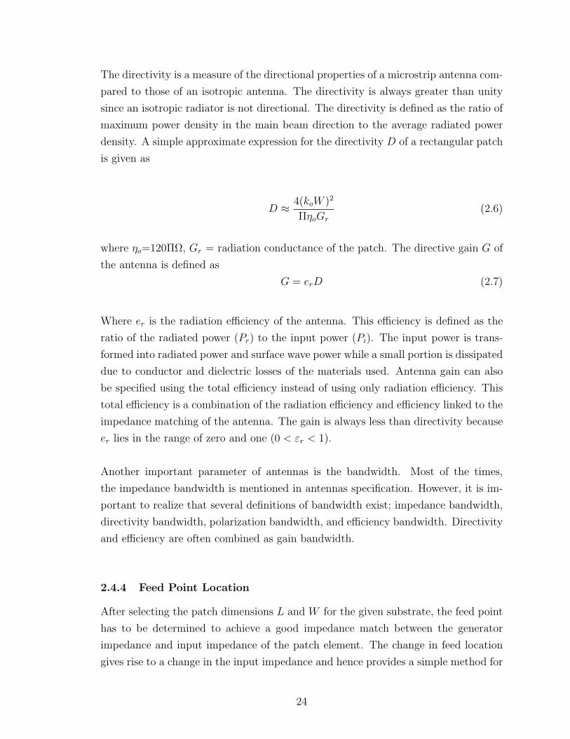
The directivity is a measure of the directional properties of a microstrip antenna com-
pared to those of an isotropic antenna. The directivity is always greater than unity
since an isotropic radiator is not directional. The directivity is defined as the ratio of
maximum power density in the main beam direction to the average radiated power
density. A simple approximate expression for the directivity D of a rectangular patch
is given as
D ≈ 4(koW )2
ΠηoGr
(2.6)
where ηo=120ΠΩ, Gr = radiation conductance of the patch. The directive gain G of
the antenna is defined as
G = erD (2.7)
Where er is the radiation efficiency of the antenna. This efficiency is defined as the
ratio of the radiated power (Pr) to the input power (Pi). The input power is trans-
formed into radiated power and surface wave power while a small portion is dissipated
due to conductor and dielectric losses of the materials used. Antenna gain can also
be specified using the total efficiency instead of using only radiation efficiency. This
total efficiency is a combination of the radiation efficiency and efficiency linked to the
impedance matching of the antenna. The gain is always less than directivity because
er lies in the range of zero and one (0 < εr < 1).
Another important parameter of antennas is the bandwidth. Most of the times,
the impedance bandwidth is mentioned in antennas specification. However, it is im-
portant to realize that several definitions of bandwidth exist; impedance bandwidth,
directivity bandwidth, polarization bandwidth, and efficiency bandwidth. Directivity
and efficiency are often combined as gain bandwidth.
2.4.4 Feed Point Location
After selecting the patch dimensions L and W for the given substrate, the feed point
has to be determined to achieve a good impedance match between the generator
impedance and input impedance of the patch element. The change in feed location
gives rise to a change in the input impedance and hence provides a simple method for
24
impedance matching. The feed point is selected such that the input resistance Rinis
equal to the feed line impedance, usually taken to be 50Ω.
2.4.5 Polarization
The polarization of a rectangular patch antenna is linear and directed along the res-
onating dimension, when operated in the dominant mode. Large bandwidth patch
antennas may operate in the higher order mode also. The radiation pattern and
polarization for these modes can be different from the dominant mode. Another
source for cross-polarization is the fringing field along the no radiating edges. These
fields are oriented 90 degrees with respect to the field at the radiating edges. Their
contribution to the radiation fields in the E and H planes is zero. However, in the
intercardinal planes, even the ideal, single mode patch will radiate cross-polarized
fields. The cross-polarization level increases with substrate thickness. Polarization of
the antenna can be changed mechanically or electronically. For the electronic tuning,
PIN diodes or varactor diodes can be used [2]. Polarization diversity used in mobile
communications to account for the reduction in signal strength due to fading.
25

Chapter Three
Microstrip Patch Antenna Design and Simulation Results
This chapter will discuss the procedures used to design the configurations of the pro-
posed microstrip patch antenna. Also, in this chapter, the radiation characteristics
for each of the designs will be discussed.
3.1 Review of Relevant Works
The approaching maturity of microstrip antenna technology coupled with the in-
creasing demand and applications for such devices has resulted in a huge volume of
research work in the field of microstrip antennas. The most relevant publications for
this specific research include ”Vertically Multilayer-stacked Yagi antenna with Sin-
gle and Dual polarizations” by Olivier Kramer, Tarek Djerafi, and Ke Wu [14], and
”Microstrip Yagi Array Antenna for Mobile Satellite Vehicle Application” by John
Huang, and Athur C. Densmore [15].
In the first paper, high gain and compact stacked multilayered Yagi antennas were
proposed and demonstrated at 5.8 GHz for a local positioning system. The proposed
structure was made of vertically stacked Yagi like parasitic director elements to ob-
tain a high antenna gain. Two different antenna configurations were proposed. The
first one based on a dipole geometry for single polarization and the second one on
a circular patch to achieve dual polarization. The result from this research work
presents a very directive and symmetric radiation pattern.
The work also suggests that the proposed designs provide a number of advantages
compared to uni-planar Yagi antennas. First, the usage of a third dimension (the
vertical dimension) that has not been widely used in the design of microstrip anten-
nas, allows an effective reduction in size, and footprint. Second, a high permittivity
26

substrate can be used, reducing spacing between the directors, which is critical for a
high-density integration between antenna and circuits. Third, wide bandwidth char-
acteristics can be achieved by implementing dual polarization designs based on the
Yagi antenna concept, and coupling-based feed mechanisms. Finally, the design of
such antennas over millimeter-wave and terahertz ranges where the substrate spac-
ing between Yagi antenna elements can naturally be made compatible with current
three-dimensional circuit processing techniques.
In the work done by Huang and Densmore, a very low profile and medium gain an-
tenna for satellite vehicle application was proposed. The design contained an antenna
active patch (driven element) and a parasitic patch (reflector and director elements)
located on the same horizontal plane. They suggested that in order for microstrip
patches to function similarly to the standard Yagi array antenna, the adjacent patches
need to be placed closely to each other so that a significant amount of coupling can be
obtained through surface waves in the substrate. They also proposed the dimension
ratio between the director patch and the driven element patch to be between 0.8 and
0.95; The distance between the centers of the reflector and the driven elements to be
about 0.35 free-space wavelengths, while the separation between the centers of the
director and driven elements to be approximately 0.3 free-space wavelength.
3.2 Microstrip Patch Antenna Design
Based on the microstrip patch antenna design considerations mentioned in section
2.4, Duroid 5870/5880 was chosen as the dielectric substrate for the antenna. This
material is lightweight, and possesses a low dielectric constant (ϵr = 2.33). It also
has uniform electrical properties over a wide frequency range. In order to achieve a
high radiation power without increasing the antenna weight and the dielectric loss, a
1.575 mm thick substrate is selected from the available commercial duroid substrate
[16]. As show in the figure 3.1 a patch length (L) of 41mm and width (W) of 37.5mm
are calculated using equations 2.1-2.7 for a resonant frequency of 2.4GHz. The feed
position must be located at a point on the patch where the input impedance is 50
ohms for the resonant frequency. The equations used to calculate the exact feed po-
sition are very complex. However, by using equation 3.1 an initial estimate of the
feed location can be calculated [17].
27

Figure 3.1: Rectangular microstrip patch antenna configuration
Rin ≈ Rr
2[1− sin(
Π
L.yf )] (3.1)
Where
Rin - Input resistance
yf - Position of feed from patch edge
L - Patch Length
Rr - Radiating resistance (for W < λ0, Rr = 90. (λ0)2
W 2 )
As a result, an approximate of 14.5mm is calculated for yf , which will be optimized
by the simulation software to achieve a 50 ohms antenna input impedance.
Typically, the size of the ground plane is assumed to be infinite during the anal-
ysis and design of microstrip patch antennas. In an actual application only a finite
size ground plane can be implemented. The implementation of a finite ground plane
induces diffraction of radiation from the edges of the ground plane, resulting in a
change in radiation pattern, radiation conductance, and resonant frequency. But, if
the size of the ground plane is greater than the patch dimensions by approximately
six times the substrate thickness all around the periphery, a similar radiation char-
28
acteristic for finite and infinite ground plane can be obtained [2].
3.3 Simulation Results
As explained in section 1.4, using the FDTD method to model an antenna has many
advantages. Such as, direct implementation of Maxwell’s curl equations, capability of
predicting broadband frequency response, analyzing structures using different types
of materials, and provides a real-time animation display. There is available different
commercial antenna simulation software that uses FDTD method. EMPro is a three
dimensional full wave electromagnetic solver that uses FDTD and Finite Element
method (FEM) to run analyses both in the frequency domain and in the time do-
main. Besides the available FDTD method, EMPro has a parameterization feature
that can be used to optimize the design to achieve better radiation characteristics.
The simulation results of the designed rectangular patch antenna radiation character-
istics (radiation pattern, antenna gain and return loss) using EMPro 3D simulation
software are presented in the following sections.
3.3.1 Radiation Pattern
In order to compare the change in radiation characteristics for the proposed designs,
the radiation characteristics for a regular microstrip patch antenna are presented.
Figures 3.2 - 3.5 present the simulated 2D cut view and 3D far zone E-plane radiation
patterns for this antenna. These results show that the microstrip patch antenna
mainly radiates in the vertical direction. This is in agreement with the theoretical
radiation pattern for these structures. It is also observed that the radiation pattern
possess a high directivity and symmetry [2][18].
29

Figure 3.2: 2D (phi=0 degrees) cut view of E- field
Figure 3.3: 3D far zone total E-Field distribution
30

Figure 3.4: 3D far zone E-Field distribution (Theta view)
Figure 3.5: 3D far zone E-Field distribution (Phi view)
3.3.2 Antenna Gain
As shown in figures 3.6 and 3.7 a maximum antenna gain of 7.083dBi with a main
lobe in the direction of theta = 0 degrees and phi = 0 degrees was obtained. The
31

simulated gain is a little higher compared to the results reported by Bhartia, Bahl,
and Garg [2].
3.3.3 Return Loss
The simulated S-parameter versus frequency and the steady state parameters in the
time domain at 2.4GHz are presented in figure 3.8. It can be seen that the simulated
center frequency is slightly shifted from the designed target, but still very close to
2.4GHz, and an input impedance of 48.718 Ohms is obtained, which is fairly close to
the standard 50 Ohms antenna input impedance.
3.4 Directors and Reflectors Design
The design of a microstrip Yagi antenna implements a similar principle as conven-
tional Yagi-Uda dipole array, where the electromagnetic energy is coupled from the
driven element dipole through space into the parasitic diploes and then reradiated to
form a directional beam. In a microstrip Yagi array, the electromagnetic energy is
coupled from the driven patch to the parasitic patches not only through space, but
also by surface waves in the substrate. Unlike a dipole antenna, the microstrip patch
radiates primarily in its broadside direction. As a consequence, the adjacent patches
need to be placed close to each other (0.15λ0 to 0.2λ0 ) in order to function similar
to Yagi dipoles [15].
The parasitic elements of the microstrip Yagi antenna operate by re-radiating their
energy in a slightly different phase to that of the driven element which reinforce the
driven element signal in some directions and cancel out in others. The amplitude and
phase of the induced current depend on the separation between the parasitic elements
and the driver element. Also, the length of the parasitic elements affects the induced
current. In order to obtain the required phase shift the parasitic element can be made
either inductive or capacitive. If the parasitic element is made inductive, the induced
currents are in such a phase that they reflect the power away from the parasitic el-
ement. This causes the microstrip patch antenna to radiate more power away from
it. These types of elements are known as reflectors. In order to make these elements
inductive their resonant length should be longer compared to the patch length. If the
parasitic element is made capacitive, the induced currents are in such a phase that
32

Figure 3.6: 2D (phi=0 degrees) cut view of the gain
Figure 3.7: 3D far zone total gain
33

Figure 3.8: Return loss (S11) and steady state parameters
they direct the power radiated by the whole antenna in the direction of the parasitic
element. These types of elements are known as directors [14][15].
In the following sections, the results from the two most significant designs will be
discussed and analyzed. It needs to be noted that more designs were studied, but
their results were not good enough to be included in this document.
3.5 Design 1 : Rectangular Reflector and Four Rectangular Directors
The configuration of the proposed microstrip patch antenna is composed by four
directors and one reflector as shown in figure 3.9. The same substrate used for the
microstrip patch is used to support the directors and reflector on the top of the patch.
In order to reduce the overall weight of the design, the thickness of the substrate for
the directors and the reflector is chosen to be 0.794mm. The entire size of the de-
signed structure is optimized as shown in table 3.1 in order to achieve a horizontal
radiation with the highest possible gain.
34
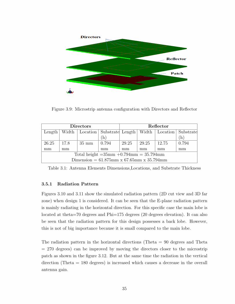
Figure 3.9: Microstrip antenna configuration with Directors and Reflector
Directors ReflectorLength Width Location Substrate
(h)Length Width Location Substrate
(h)26.25mm
17.8mm
35 mm 0.794mm
29.25mm
29.25mm
12.75mm
0.794mm
Total height =35mm +0.794mm = 35.794mmDimension = 61.875mm x 67.65mm x 35.794mm
Table 3.1: Antenna Elements Dimensions,Locations, and Substrate Thickness
3.5.1 Radiation Pattern
Figures 3.10 and 3.11 show the simulated radiation pattern (2D cut view and 3D far
zone) when design 1 is considered. It can be seen that the E-plane radiation pattern
is mainly radiating in the horizontal direction. For this specific case the main lobe is
located at theta=70 degrees and Phi=175 degrees (20 degrees elevation). It can also
be seen that the radiation pattern for this design possesses a back lobe. However,
this is not of big importance because it is small compared to the main lobe.
The radiation pattern in the horizontal directions (Theta = 90 degrees and Theta
= 270 degrees) can be improved by moving the directors closer to the microstrip
patch as shown in the figure 3.12. But at the same time the radiation in the vertical
direction (Theta = 180 degrees) is increased which causes a decrease in the overall
antenna gain.
35
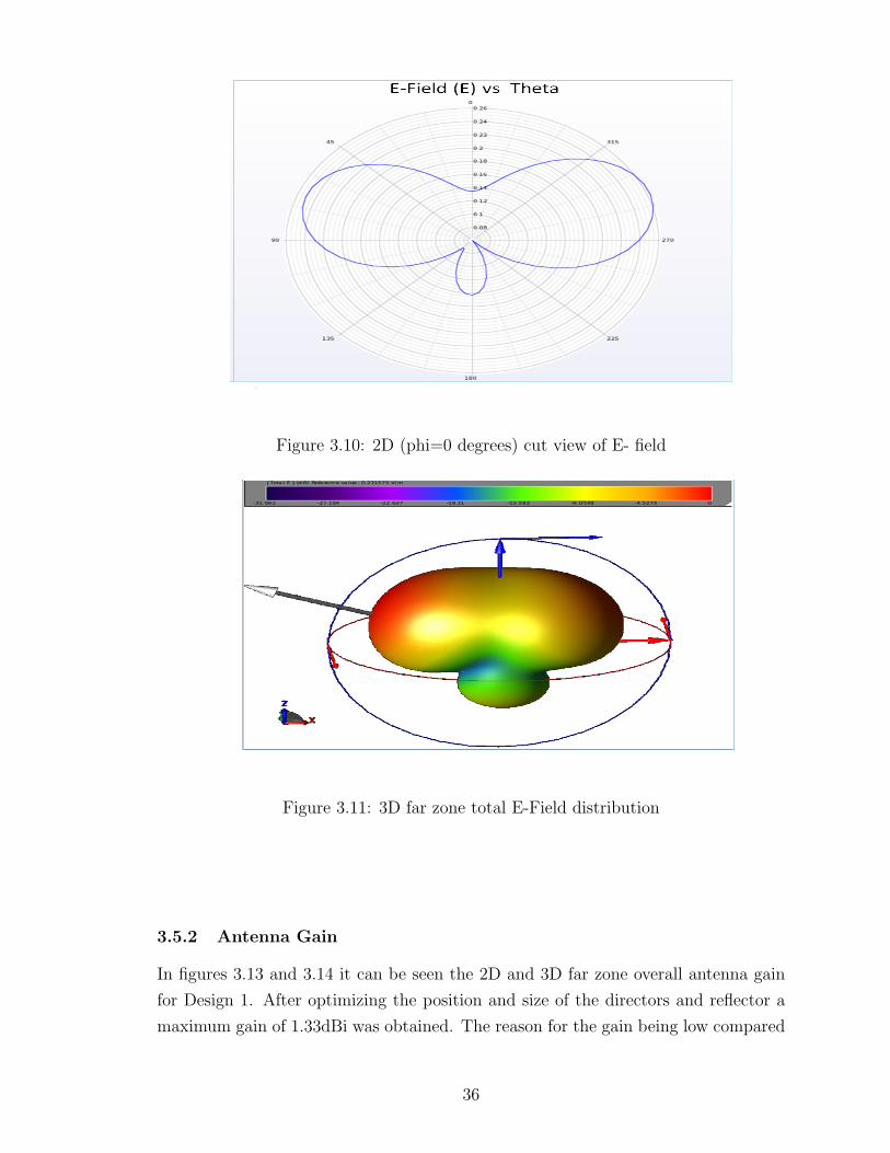
Figure 3.10: 2D (phi=0 degrees) cut view of E- field
Figure 3.11: 3D far zone total E-Field distribution
3.5.2 Antenna Gain
In figures 3.13 and 3.14 it can be seen the 2D and 3D far zone overall antenna gain
for Design 1. After optimizing the position and size of the directors and reflector a
maximum gain of 1.33dBi was obtained. The reason for the gain being low compared
36

Figure 3.12: Radiation pattern variation with director positions
to the rectangular patch antenna is that the microstrip patch antenna covers a wide
solid angle which makes it best suited for applications that require a wide coverage
in short distances.
As reported in [2][19], although most horizontally polarized antennas have a low gain,
it has been predicted that using horizontally polarized antenna at both the transmitter
and receiver will result in 10dB more power as compared to the power received using
vertically polarized antennas at both end of the link. The reason is that horizontally
polarized antennas are less likely to pick up manmade interference, which is normally
vertically polarized. When antennas are located near dense forests, horizontally po-
larized waves suffer smaller losses compared to vertically polarized waves, especially
above 100MHz. Small changes in antenna location do not cause large variations in
the field intensity of horizontally polarized waves when an antenna is located among
trees or buildings. When vertical polarization is used, a change of only a few feet in
the antenna location may have a significant effect on the received signal strength [20].
3.5.3 Return Loss
The S11-parameter (return loss) versus frequency and time domain steady state pa-
rameters at 2.4GHz are presented in figure 3.15. It is observed that the center resonant
37

Figure 3.13: 2D (phi=0 degrees) cut view of the gain
Figure 3.14: 3D far zone total gain
frequency has been shifted to a lower frequency due to the reactance variation of the
antenna due to the reflector and directors. The input impedance of the antenna has
also decreased to 41.734 Ohms, and it has become more reactive.
A better microstrip patch antenna gain of 2.033 dBi is obtained by removing the
extension of the substrate beyond the dimensions of reflector and directors except for
38

Figure 3.15: Return loss (S11) and steady state parameters
the material necessary to fix the directors and reflector with the patch. The proposed
design is shown in figure 3.16. An input impedance of 42.3 Ohms, which is closer to
the 50 Ohms standard antenna input impedance is achieved, whereas the resonance
frequency remained the same.
Figure 3.16: Microstrip patch antenna configuration with directors and reflector
39

Figure 3.17: 3D far zone total gain
40

3.6 Design 2 : Loop Director and Rectangular Reflector
The configuration of the proposed microstrip patch is composed of one loop director
and one rectangular reflector as shown in figure 3.18. It was observed from design
1 that the radiation pattern of the microstrip patch antenna is more uniform and
horizontally directed when the four directors are placed close to each other. Based on
this observation it was decided to replace the four directors with a loop to improve
the radiation characteristics of the proposed antenna. The same substrate type and
thickness was used for the loop director as the rectangular directors in design 1.The
entire size of the designed structure is optimized as shown in table 3.2 in order to
achieve a horizontal radiation with the highest possible gain.
Figure 3.18: Microstrip patch antenna configuration with loop director
Director ReflectorsOuterRadius
InnerRadius
Location Substrate(h)
Length Width Location Substrate(h)
29.615mm
17.5mm
35 mm 0.794mm
36.25mm
36.25mm
23 mm 0.794mm
Total height = 35mm + 0.794mm =35.794 mmDimensions = 61.875mm x 67.65mm x 35.794mm
Table 3.2: Antenna Elements Dimensions,Locations, and Substrate Thickness
41

3.6.1 Radiation Pattern
Figures 3.19 and 3.20 present the 2D cut view and 3D far zone simulation result of
the E-plane radiation pattern of the microstrip patch antenna configuration with a
loop director. As shown in figure 3.19 a fully horizontal (0 degrees elevation) and
symmetric radiation pattern is obtained, Also the vertical direction radiation was
suppressed and made very low which helps to improve the overall performance of the
antenna.
Figure 3.19: 2D (phi=0 degrees) cut view of E- field
Figure 3.20: 3D far zone total E-Field distribution
42

3.6.2 Antenna Gain
The simulation results of the 2D cut view and 3D far zone gain for the microstrip
patch antenna configuration with the loop director are presented in figures 3.21 and
3.22. A maximum gain of 1.972 dBi is obtained where the main lobe is directed to
theta=90 degrees and Phi=170 degrees (0 degrees elevation). The gain is low because
the microstrip patch antenna covers a wide solid angle which makes it best suited for
applications that require a wide coverage in a short distance.
Figure 3.21: 2D (phi=0 degrees) cut view of the gain
Figure 3.22: 3D far zone total gain
43
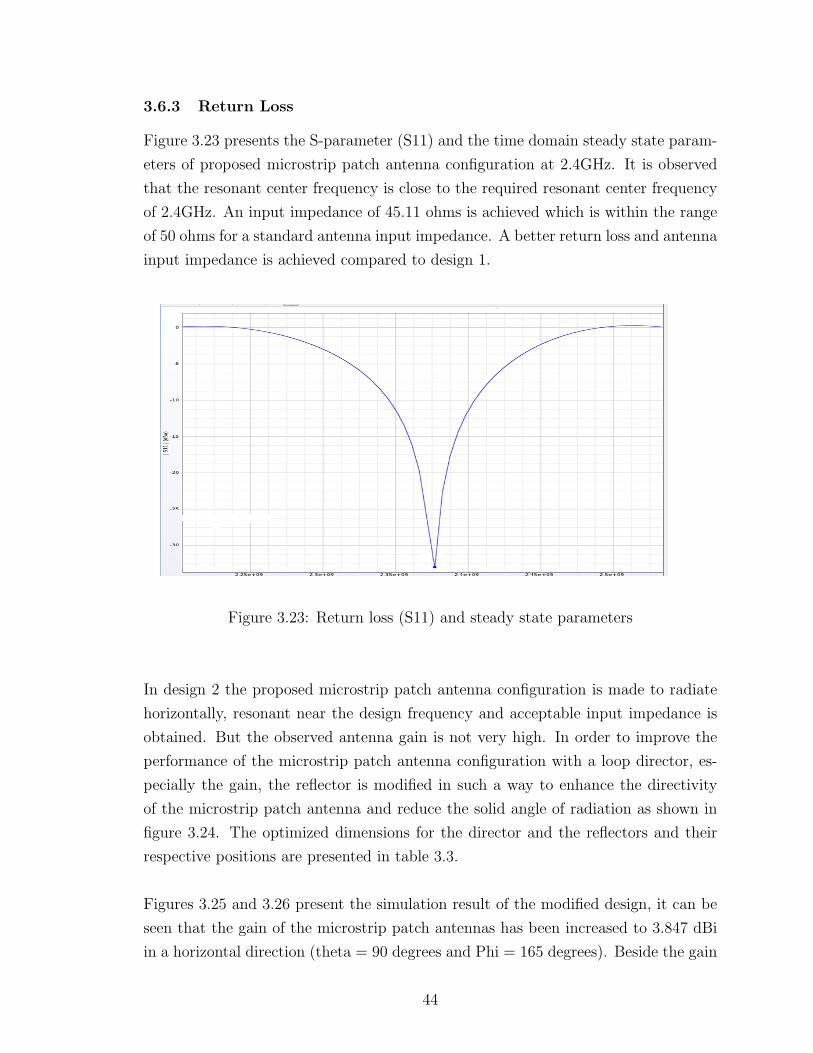
3.6.3 Return Loss
Figure 3.23 presents the S-parameter (S11) and the time domain steady state param-
eters of proposed microstrip patch antenna configuration at 2.4GHz. It is observed
that the resonant center frequency is close to the required resonant center frequency
of 2.4GHz. An input impedance of 45.11 ohms is achieved which is within the range
of 50 ohms for a standard antenna input impedance. A better return loss and antenna
input impedance is achieved compared to design 1.
Figure 3.23: Return loss (S11) and steady state parameters
In design 2 the proposed microstrip patch antenna configuration is made to radiate
horizontally, resonant near the design frequency and acceptable input impedance is
obtained. But the observed antenna gain is not very high. In order to improve the
performance of the microstrip patch antenna configuration with a loop director, es-
pecially the gain, the reflector is modified in such a way to enhance the directivity
of the microstrip patch antenna and reduce the solid angle of radiation as shown in
figure 3.24. The optimized dimensions for the director and the reflectors and their
respective positions are presented in table 3.3.
Figures 3.25 and 3.26 present the simulation result of the modified design, it can be
seen that the gain of the microstrip patch antennas has been increased to 3.847 dBi
in a horizontal direction (theta = 90 degrees and Phi = 165 degrees). Beside the gain
44

Figure 3.24: Microstrip antenna configuration with three reflectors
ReflectorsDirector Center reflector Side reflector
OuterRadius
InnerRadius
Location Substrate(h)
Length Width Location Substrate(h)
29.615mm
17.5mm
30 mm 0.794mm
36.25mm
36.25mm
12.81mm
44.35mm
ReflectorsLocation Substrate(h)13 mm 0.794 mm
Total height = 30mm + 0.794mm =30.794 mmDimension = 61.875mm x 67.65mm x 30.794mm
Table 3.3: Antenna Elements Dimensions,Locations, and Substrate Thickness
enhancement due to the added side reflectors the entire antenna structure height is
reduced by 5 mm as shown in table 3.3. The resonant center frequency is also slightly
shifted toward the design center frequency and an input impedance of 56.77 ohms is
obtained as shown in figure 3.27.
45

Figure 3.25: 2D (phi=0 degrees) cut view of the gain
Figure 3.26: 3D far zone total gain
46

Figure 3.27: Return loss (S11) and steady state parameters
47

Chapter Four
Conclusion and Future Work
4.1 Conclusion
This research introduced and investigated a novel concept in the design of microstrip
patch antennas with a radiation pattern in the horizontal direction. Two different
antenna configurations with directors and reflectors to guide the radiated power in
the horizontal direction were designed and simulated. The characteristics of the two
proposed designs with respect to various parameters such as reflector dimensions, di-
rector dimensions, and spacing between these elements and the microstrip patch have
been studied. The simulated results of the radiation pattern showed that the radi-
ated power was horizontally directed on both designs which was insignificant for the
standard microstrip patch antenna. The design with four rectangular directors and
one rectangular reflector yielded a radiation pattern with an elevation of 20 degrees
with a maximum gain of 2.033dBi. The proposed antenna structure has dimensions of
61.785mm x 67.65 mm and total height of 35.794mm. The overall size of the proposed
antenna structure is compact compared to commercially available antenna of its type.
The results from the design with one loop director and three rectangular reflectors
yielded a radiation pattern with an elevation of 0 degrees with a maximum gain of
3.847 dBi. The compactness of the overall antenna structure was further improved
to 61.875mm x 67.65mm and a total height of 30.794mm.The input impedance and
resonance center frequencies for both designs were close to the calculated values ac-
cording to the simulation results.
This work suggests that the proposed antennas configurations provide a light-weight,
compact, low cost and better signal strength in horizontal direction compared to the
regular microstrip patch antenna. These antennas present an excellent candidate for
emerging wireless communications at 2.4 GHz frequency that require a transfer of
48

large amount of data in rapid bursts, which include Bluetooth and WiFi (802.11).
4.2 Future Work
The simulation results are good enough to justify fabrication of the proposed anten-
nas on hardware to check the actual radiation performance. The investigation has
been limited to theoretical studies and simulations due to lack of testing facilities at
2.4GHz frequency. In order to enhance the gain and other radiation performances of
the antennas, additional directors/reflectors can be added accordingly. Using thicker
substrates for those applications where the weight of the antenna is not an issue could
improve the performance of the proposed designs. It is also expected that the size
of the proposed antennas can be reduced approximately by half for 5GHz applications.
49

References
[1] Constantine A. Balanis, ”Antenna Theory: Analysis and Design, 3rd Edition,”
John Wiley and Sons, Inc. Hoboken, New Jersey 2005.
[2] P. Bhartia , Inder Bahl , R. Garg, and A. Ittipiboon, ”Microstrip Antenna Design
Handbook,” Artech House Inc. Norwood, MA 2001.
[3] Jagdish. M. Rathod, and Y.P.Kosta, ”Development of Feed for Parabolic Reflec-
tor Antenna,” International Journal of Engineering and Technology, Vol. 1, No.
1, April, 2009, pp.1793-8236.
[4] IEEE Standard Definitions of Terms for Antennas, Transactions on antennas
and propagation, May 1969.
[5] Edited by William A. Imbriale, Steven S. Gao and Luigi BocciaJohn, ”Space
Antenna Handbook,” Wiley and Sons Ltd. West Sussex, UK 2012.
[6] C.-C. Lin, L.-C. Kuo, and H.-R. Chuang, ”A Horizontally Polarized Omnidirec-
tional Printed Antenna for WLAN Applications,” IEEE Transactions On An-
tennas And Propagation, Vol.54, No. 11, November 2006, pp.3551-3556.
[7] ”Antenna Fundamentals,” http://etd.lib.fsu.edu/theses/available/etd-04102004-
143656/unrestricted/Chapter2.pdf.
[8] Dr. Steven R. Best, ”Antenna Properties and their impact on Wireless System
Performance,” Cushcraft Corporation, Manchester, NH 03013.
[9] Weili Ma, ”Discrete Green’s Function Formulation of the FDTD Method and its
Application,” Department of Electronic Engineering, Queen Mary University of
London, United Kingdom, February 2004.
[10] ”EMPro 3D EM Simulation Software,” http://www.home.agilent.com/en/pc-
1297143/empro-3d-em-simulation-software.
50

[11] Mouloud Challal1, Arab Azrar1 and Mokrane Dehmas, ”Rectangular Patch An-
tenna Performances Improvement Employing Slotted Rectangular shaped for
WLAN Applications,” IJCSI International Journal of Computer Science Issues,
Vol. 8, Issue 3, No. 1, May 2011, pp.254-258.
[12] Shiv Kaushik Varanasi, ”Investigations On Cavity Backed Wideband Microstrip
Patch Antennas With Enhanced Performance For Wireless Communication Ap-
plications,” San Diego State University, Fall 2010.
[13] RongLin Li, Gerald DeJean, Moonkyun Maeng, Kyutae Lim, Stephane Pinel,
Manos M. Tentzeris, and Joy Laskar, ”Design of Compact Stacked-Patch Anten-
nas in LTCC Multilayer Packaging Modules for Wireless Applications,” IEEE
Transactions On Advanced Packaging, Vol. 27, No. 4, November 2004,
pp.581-589.
[14] Olivier Kramer, Tarek Djerafi, and Ke Wu, ”Vertically Multilayer-Stacked Yagi
Antenna With Single and Dual Polarizations,” IEEE Transactions On Antennas
And Propagation, Vol. 58, No. 4, April 2010, pp.1022-1030.
[15] John Huang, and Arthur C. Densmore, ”Microstrip Yagi Array Antenna for Mo-
bile Satellite Vehicle Application,” IEEE Transactions On Antennas And Prop-
agation, Vol. 39, No. 7, July 1991, pp.1024-1030.
[16] . ”RT/duroid-High Frequency Laminates,” http://www.rogerscorp.com/acm/products/10/RT-
duroid-5870-5880-5880LZ-High-Frequency-Laminates.aspx.
[17] ”Satellite Communications,” http://www.odyseus.nildram.co.uk/.
[18] Gray A Thiele, ”Analysis of Yagi-Uda-Type Antennas,” IEEE Transactions On
Antennas And Propagation, Vol. Ap-17, So. 1, January 1969, pp.24-31.
[19] C.Soras, M.Karaboikis, G. Tsachtsiris and V. Markios, ” Analysis and Design of
an inverted-F antenna printed on a PCMCIA Card for 2.4GHz ISM Band,” IEEE
Antenna’s and Propagation Magazine, Vol 44, No. 1, February 2002, pp.37-42.
[20] J. E. RHODES Lieutenant General, U.S. Marine Commanding General Ma-
rine Corps Combat Development Command, ”Antenna Handbook,” Distribu-
tion: 144 000062 00.
51