USPAS June 2015 Rutgersuspas.fnal.gov/materials/15Rutgers/AMVF_Alternative_Surface...Anne‐Marie...
55
This week Program Alternative Processes for bulk Nb Technology Today, Monday 22 PM SRF Materials Other than Bulk Nb Tuesday 23 PM RF, Cryogenic & Other Methods for SRF Materials Wednesday 24 PM Surface/Material Analyses for SRF Materials Thursday 25 AM Anne‐Marie Valente‐Feliciano ‐ Alternative Surface Preparation ‐ USPAS June2015 ‐ Rutgers
Transcript of USPAS June 2015 Rutgersuspas.fnal.gov/materials/15Rutgers/AMVF_Alternative_Surface...Anne‐Marie...
This week Program
Alternative Processes for bulk Nb TechnologyToday, Monday 22 PM
SRF Materials Other than Bulk NbTuesday 23 PM
RF, Cryogenic & Other Methods for SRF MaterialsWednesday 24 PM
Surface/Material Analyses for SRF MaterialsThursday 25 AM
Anne‐Marie Valente‐Feliciano ‐Alternative Surface Preparation ‐USPAS June2015 ‐ Rutgers

Anne‐Marie Valente‐FelicianoThomas Jefferson National Accelerator Facility
USPAS June 2015 Rutgers

Standard Nb Surface Treatments
Anne‐Marie Valente‐Feliciano ‐Alternative Surface Preparation ‐USPAS June2015 ‐ Rutgers
From Last week …
Required Procedures for Qualifying SRF Cavities •Degreasing surfaces to remove contaminates •Chemical removal of exterior films incurred from welding•Removal of damage layer of niobium from fabrication (150 µm)•Removal of hydrogen from bulk Nb•Mechanical tuning•Chemical removal of internal surface for clean assembly (10‐20 µm)Additional “cleaning” steps if Electropolishing(EP) is used•High Pressure Rinsing (HPR) to remove particulates from interior surfaces (incurred during chemistry and handling) •Drying of cavity for assembly in cleanroom(reduce risk of particulate adhesion and reduce wear on vacuum systems)•Clean assembly •Clean evacuation•Low‐temperature baking

Conventional Surface Preparation for SRF Cavities
• Buffered Chemical Polishing: HF : HNO3 : H3PO4
(ratio 1:1:1 or 1:1:2)HNO3 : Oxiding agentHF : Transforms Nb2O5 into a water soluble saltH3PO4 : Reaction moderator or Buffer
• ElectroPolishing: HF : H2SO4 (ratio 1:9)
Anne‐Marie Valente‐Feliciano ‐ Alternative Surface Preparation ‐ USPAS June2015 ‐ Rutgers
Both etching and EP electrolyte are composed of very harmful components both for humans and the environment, needing preventive and expensive mitigation proceduresEfforts around the world to get rid of the most harmful components

Standard BCP: HF : HNO3 : H3PO4
Modified BCP: HF : HNO3 : H2SO4 (ratio 1:1:2) at 78°CY. Uzel, K. Schnitzke, N. Krause: Appl. Phys., A30 (1983) p.185
HF : HNO3 : H2SO4 (ratio 1:1:1) RTC. Z. Antoine, A. Aspart, J.P. Charrier, H. Safa, B.Visentin, Proc 9th Workshop on SC RF, (1999) Santa Fe
Alternatives to BCP
Anne‐Marie Valente‐Feliciano ‐ Alternative Surface Preparation ‐ USPAS June2015 ‐ Rutgers
Introduction of LESS HAZARDOUS COMPONENTS in the standard BCP
For example: HF NH4F
HNO3 H2O2
NH4F + HCl + H2O2 + H3PO4 at room temperatureSeveral percentages studied, the best results were obtained with the
NH4F : HCl : H2O2 : H3PO4 in the 2:2:4:1 ratio with (60g/l) of NH4FV. Palmieri, F. Stivanello, C. Roncolato, M. Valentino –Proc. 10th SC RF workshop, 2001 Tsukuba

2° International TESLA Workshop, DESY, Hamburg ,August 1991
Composition HF : H2SO4 : Lactic acid in the ratio 18 : 21 : 61
Current Density = 90‐110 mA/cm2
Voltage = 15‐18 VTemperature = 50‐60 °C
Note: Lactic acid solutions can be explosive
Improved Methods for Electrochemical Polishing of Nb Superconducting cavitiesV.M. Efremov, L.M. Sevryukova, M. Hein, L. Ponto
Alternatives for EP: lactic acid
Anne‐Marie Valente‐Feliciano ‐ Alternative Surface Preparation ‐ USPAS June2015 ‐ Rutgers

Buffer Electro‐Polishing (BEP)
Anne‐Marie Valente‐Feliciano ‐Alternative Surface Preparation ‐USPAS June2015 ‐ Rutgers
Major Benefits:1. Smoothest surface finish
BEP 35nm vs BCP 1274nm better RF performance
2.Highremoval rate BEP 4.09μm/min vs. EP 0.38μm/min
potential huge reduction in cavity preparation cost
Current Status:1.BEP on large grain cavity reaches 32MV/m2.BEP on regular fine grain cavity reaches 23MV/m (quench limited)3.The inner surfaces of cavities look very smooth for both large and fine grain cavities after BEP4.Next, compare with standard EP
Buffered Electropolishing (BEP) uses an acid mixture of lactic, sulfuric, hydrofluoric acids as electrolyte. Partial replacement of sulfuric acid by lactic acid makes handling the electrolyte safer.

There are a lot of horror stories about HF:Hydrofluoric acid is a highly corrosive solutionIf it is accidentally released, it forms an aerosol acid cloud which can cause serious bone damage anddeath by burns to the skin, tissue or lungs. Even minor exposure can cause skin burns and blindness.
A plethora of devastating histories in refineries using Hydrofluoric acid
•On contact, HF passes through skin and tissue.•Contact with HF does not cause immediate pain, so systemic poisoning begins before the person is
aware•Because its action can be delayed for many hours, it can distribute through out the body, causing the
erosion of bones.•F‐ions bind to Ca++and Mg++ions to form in soluble salts•(CaF2 and MgF2 salts form some natural gemstones).•In the body, Ca and Mg ions are used to mediate a variety of physiological processes, such as muscle
movement.•Cardiac arrests have been reported from concentrated acid burns to as little as 2.5% of exposed body
surface area
Anne‐Marie Valente‐Feliciano ‐ Alternative Surface Preparation ‐ USPAS June2015 ‐ Rutgers
Alternatives for EP: getting rid of HF?
The Chemical/Electro‐chemical Polishing of 20,000+ cavities for ILC would require several hundred Tons of HF
Phasing out the use of HF and enacting a safer alternative would be a big asset

EP Alternative: Ionic liquidsIonic liquids are defined today as liquids which solely consist ofcations and anions and which by definition must have a melting pointof 100 °C or below.In the middle of the 1990s the term ‘‘room temperature molten salt’’was definitely replaced by ‘‘ionic liquid’’.The ‘‘room temperature molten salts’’ were regarded as uncommonand as a curiosity for a while. The situation has changed dramaticallythroughout the recent 3 years
Anne‐Marie Valente‐Feliciano ‐ Alternative Surface Preparation ‐ USPAS June2015 ‐ Rutgers
Ionic liquids are going to represent a main stream in various fieldsof chemistry and physical chemistry!
Imagine making a liquid just by mixing two solids! And think what you could do with this liquid if it was non‐toxic, biodegradable and
could dissolve a wide range of materials.
The trend is to look for liquids that can be used to substitute thestrong and corrosive acids traditionally used as solvents in manyindustrial chemical reactions.

In exactly the same way as common salt, liquid salts consist of positively charged and negatively charged ions, thoughthey are not simple ions like sodium and chloride but are much larger and more complex, and unable to form easily acrystal lattice. If even a small amount of heat is applied to them, the solid crystalline structure disintegrates and thebonds between the ions are broken. The salt becomes a liquid – an ionic liquid.
Salt flats in California: A lake has evaporated, leaving behind a layer of salt.
Anne‐Marie Valente‐Feliciano ‐Alternative Surface Preparation ‐USPAS June2015 ‐ Rutgers
Benefits Non‐aqueous Non‐volatile Non‐toxic Highly conducting Improved current efficiencies Recyclable Decrease hydrogen evolution Decreased emissions Iron Residue Recovery Costs comparable to organic solvents Bacterial growth inhibition Micro finish enhancement Reduced occurrence of intergranular
attack ( preferential etching) Reflective finish Polished surface can withstand
cleaning and autoclaving Any size metal can be electropolished
Electropolishing solutions based on Ionic Liquid Technology

HF‐free electropolishing
Anne‐Marie Valente‐Feliciano ‐Alternative Surface Preparation ‐USPAS June2015 ‐ Rutgers
Dosage and UseTake 1 to 3 teaspoons daily.It is best mixed with approximately2 oz. of juice per teaspoon.
Choline Chlorine enhances and accelerates growth in animals during times of rapid development (common poultry feed additive).
Choline is important for• fetal development and for babies/children. Human milk contains high amounts of choline.•cell membrane structure, for synthesizing folic acid and vitamin B12, and for protecting the liver from accumulating fat. (Take choline chloride supplements to protect the liver from damage, to lower cholesterol, to improve memory, to preserve prostate and to enhance mood!)
The brain has a voracious appetite for choline.
Choline is required for •synthesis of the key neurotransmitter acetylcholine•building and maintaining brain cell membranes.( Acetylcholine is vital for thought, memory and sleep, and is also involved in the control of movements)
…. and to electropolish Niobium

Anne‐Marie Valente‐Feliciano ‐ Alternative Surface Preparation ‐ USPAS June2015 ‐ Rutgers
Molecular formula C5H14ClNOMolar Mass 139.62 g.mol−1Appearance White or deliquescent crystalsMolecular Formula 302 °C (decomposes)Solubility in water very soluble
Choline chloride (2‐hydroxyethyl‐trimethylammonium) is a quaternary ammonium salt also known as Vitamin B4. It has a Choline cation with a Chloride anion.
It forms with Urea a Deep Eutectic Solvent able to dissolve many metal salts
Electropolishing with Choline Chlorine
ABBOTT Patent deposited by Shonix
Surprisingly, however, we have now found that by forming the anion of an ionic compoundfrom a hydrated metal salt and the cation from certain specific amine salts, it is possible toproduce compounds which are liquid at low temperatures (i.e. 50 °C and below), relativelyinexpensive, and relatively water insensitive.
Choline chloride and hydrated metal halides, as magnesium chloride, Copper nitrate, orCalcium chloride, … succeed in electropolishing a big variety of metals.
A. P. Abbott et al., Electrochemica acta 51 (2006) 4420‐4425

On the basis of Abbott Patent
Electropolishing of Nb was achievedby a mixture of Choline Chloride, Urea, NH4F at80°C.
Anne‐Marie Valente‐Feliciano ‐ Alternative Surface Preparation ‐ USPAS June2015 ‐ Rutgers

Bare Surface
Standard ElectropolishingUrea/Choline Cloride 3/1 + Ammonium Chloride 10g/L (190 °C; 200 mA/cm2).
Profilometry ( 500mm x 500mm scans)
Anne‐Marie Valente‐Feliciano ‐ Alternative Surface Preparation ‐ USPAS June2015 ‐ Rutgers
Ra= 785.9 nm
Ra= 248.8 nm Ra= 189.7 nm
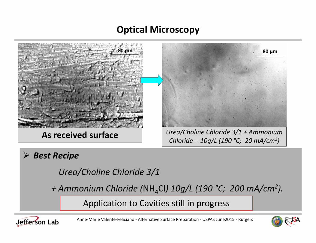
Urea/Choline Chloride 3/1 + Ammonium Chloride ‐ 10g/L (190 °C; 20 mA/cm2)
As received surface
Optical Microscopy
Best Recipe
Urea/Choline Chloride 3/1
+ Ammonium Chloride (NH4Cl) 10g/L (190 °C; 200 mA/cm2).
80 μm 80 μm
Application to Cavities still in progress Anne‐Marie Valente‐Feliciano ‐ Alternative Surface Preparation ‐ USPAS June2015 ‐ Rutgers

BIPOLAR OR PULSED REVERSE EP

Anodic Pulse “Tuned” to: • Control current distribution • Eliminates need for viscous, low water content
electrolytes , such as H2SO41, NaOH2
Cathodic Pulse “Tuned” to:• Reduce oxide/depassivate surface • Eliminate need for HF Need further understanding
Off‐Time “Tuned” to: • Heat dissipation • Replenish reacting species • Remove reaction productsNeed further optimization
Bipolar Pulse EP for Nb SRF Cavity
1) M. Inman, E. J. Taylor, and T. D. Hall Journal of The Electrochemical Society, 160 (9) E94‐E98 (2013)
2) M. Umehara, T. Saeki, H. Hayano, LINAC 2014
Anne‐Marie Valente‐Feliciano ‐Alternative Surface Preparation ‐USPAS June2015 ‐ Rutgers
Bipolar EP (pulse‐forward, reverse‐pulse technique) uses an anodic forward pulse to grow an oxide layer on the reacting surface. The anodic pulse is followed by a delay, or voltage off‐time, that dissipates the heat, removes reaction by‐products, and replenishes active agents needed for the reaction. A cathodic pulse then reverses the voltage and reduces the passive oxide layer on the reacting surface.
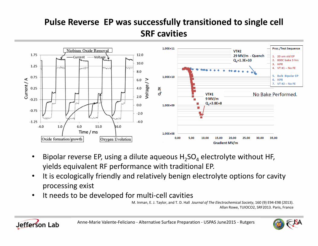
Pulse Reverse EP was successfully transitioned to single cell SRF cavities
• Bipolar reverse EP, using a dilute aqueous H2SO4 electrolyte without HF, yields equivalent RF performance with traditional EP.
• It is ecologically friendly and relatively benign electrolyte options for cavity processing exist
• It needs to be developed for multi‐cell cavities M. Inman, E. J. Taylor, and T. D. Hall Journal of The Electrochemical Society, 160 (9) E94‐E98 (2013).
Allan Rowe, TUIOCO2, SRF2013. Paris, France
Anne‐Marie Valente‐Feliciano ‐ Alternative Surface Preparation ‐ USPAS June2015 ‐ Rutgers
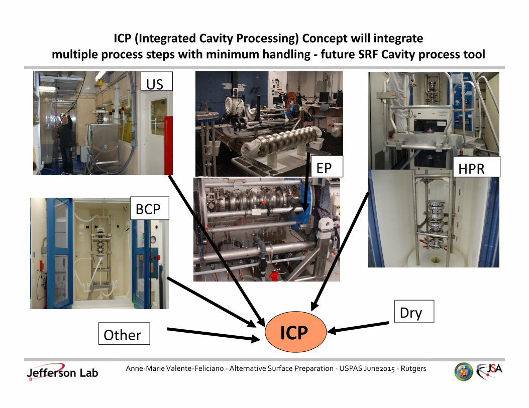
ICP
BCP
HPR
US
EP
Dry
ICP (Integrated Cavity Processing) Concept will integrate multiple process steps with minimum handling ‐ future SRF Cavity process tool
Other
Anne‐Marie Valente‐Feliciano ‐Alternative Surface Preparation ‐USPAS June2015 ‐ Rutgers

The next step, ICP
We need confident and variable multi‐parameter process control.• ICP units will integrate VEP, BCP, HPR, US, and HWR in an automated tool in a clean environment.
• The concept is to leave the cavity stationary and bring the sequential processes to the cavity.
Anne‐Marie Valente‐Feliciano ‐Alternative Surface Preparation ‐USPAS June2015 ‐ Rutgers

DRY ETCHING
Anne‐Marie Valente‐Feliciano ‐ Alternative Surface Preparation ‐ USPAS June2015 ‐ Rutgers

Although Wet acid etching (BCP or EP) is the commonly used process in processing of SRF
cavities, it has been abandoned as the fabrication process in microelectronic industry, primarily due to the isotropic
material removal
Plasma‐assisted etch process (dry etching) is the enabling process in semiconductor industry, since it can be highly selective with respect to direction and hence indispensable in patterned removal of surface material or in removal of material from non‐flat surfaces .
(a)
(b)
Schematic illustration of (a) isotropic action (wet) etching, and (b) anisotropic (dry) etching
Dry Etching vs. Wet Etching
Anne‐Marie Valente‐Feliciano ‐Alternative Surface Preparation ‐USPAS June2015 ‐ Rutgers

Motivation for dry etching for SRF cavities
• Low Cost• No wet chemistry• Environment and People friendly (compared to wet etching process)• Full control on the final surface
“Oxide –free” surface if kept under UHV A variety of surfaces can be intentionally created through plasma processing
Pure Nb2O5, or other cap layer superconducting NbN S‐I‐S Multilayer
BCP Process
Dry Process
Comparison of surface micrographstaken with KH‐3000 digital microscopewith magnification 10×350
M. Rašković, L. Vušković, S. Popović, L. Phillips, A. M. Valente‐Feliciano, S. B. Radovanov, and L. Godet, Nucl. Instrum. Methods Phys. Res. A 569, 663 (2006
Anne‐Marie Valente‐Feliciano ‐Alternative Surface Preparation ‐USPAS June2015 ‐ Rutgers

Mechanism of Plasma Etching
Nb surface
1. Generation of reactive species
2. Diffusion of reactive species
3. Adsorption on surface 4. Reactions
5. Desorption of products
Bulk Nb
2Nb (s) + 5Cl2 (g) 2NbCl5 (g) No oxidizing agent needed
Anne‐Marie Valente‐Feliciano ‐Alternative Surface Preparation ‐USPAS June2015 ‐ Rutgers
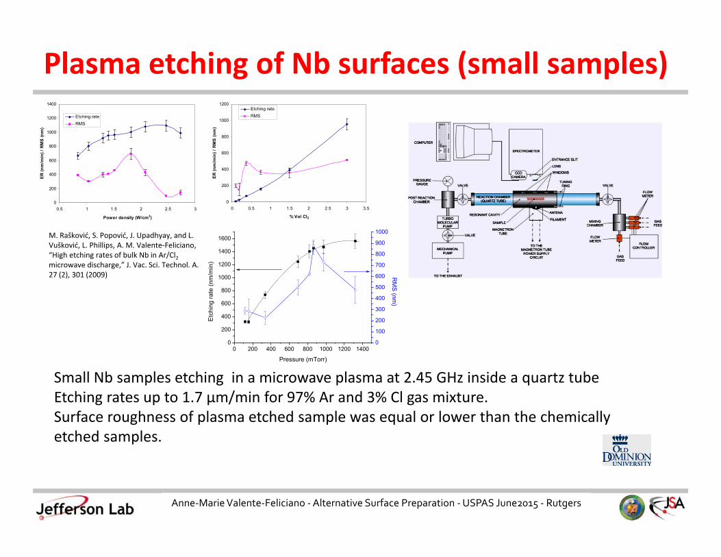
Plasma etching of Nb surfaces (small samples)
Anne‐Marie Valente‐Feliciano ‐Alternative Surface Preparation ‐USPAS June2015 ‐ Rutgers
0
200
400
600
800
1000
1200
1400
0.5 1 1.5 2 2.5 3
Power density (W/cm3)
ER (n
m/m
in) /
RM
S (n
m)
Etching rateRMS
0
200
400
600
800
1000
1200
0 0.5 1 1.5 2 2.5 3 3.5
% Vol Cl2ER
(nm
/min
) / R
MS
(nm
)
Etching rate RMS
0 200 400 600 800 1000 1200 14000
200
400
600
800
1000
1200
1400
1600
Pressure (mTorr)
Etch
ing
rate
(nm
/min
)
0
100
200
300
400
500
600
700
800
900
1000
RM
S (nm)
M. Rašković, S. Popović, J. Upadhyay, and L. Vušković, L. Phillips, A. M. Valente‐Feliciano, “High etching rates of bulk Nb in Ar/Cl2microwave discharge,” J. Vac. Sci. Technol. A. 27 (2), 301 (2009)
Small Nb samples etching in a microwave plasma at 2.45 GHz inside a quartz tubeEtching rates up to 1.7 μm/min for 97% Ar and 3% Cl gas mixture. Surface roughness of plasma etched sample was equal or lower than the chemically etched samples.

Flat Samples ‐ Surface Roughness
BCP 1:1:2, 20 m
BCP + PE
AFM scans (50 μm 50 μm)
RMS =286nmRa=215nm
RMS =215nmRa=169 nm
As receivedRMS=254nm Ra=210 nm
120 m
3‐steps PE ,120 mRMS=234nmRa=174 nm
Anne‐Marie Valente‐Feliciano ‐Alternative Surface Preparation ‐USPAS June2015 ‐ Rutgers

3‐step process
1. Pure Ar removes physisorbed gasses and organic residues from Nb surface without damaging surfaceTime 30 min, Total flow 150 sccm, Input power density 2.08 W/cm3 ,Pressure 500 mTorr
Etching rate 0nm/min2. 3 Vol% Cl2 in Ar removes surface necessary for cavity productionTime 120 min , Total flow 198.6 sccm, Input power density 2.08 W/cm3 , Pressure 550 mTorr
Etching rate 1 µm/minremoves ~120 mm of surface in 2 h3. 1.5 Vol% Cl2 in Ar removes surface under conditions more favorable for surface smootheningTime 240 min , Total flow 348.6 sccm, Input power density 1.4 W/cm3 , Pressure 1250 mTorr
Etching rate 0.5 µm/min
Anne‐Marie Valente‐Feliciano ‐ Alternative Surface Preparation ‐ USPAS June2015 ‐ Rutgers
Plasma Etching of Single Cell Nb Cavity
Plasma in The Cavity
Schematic Diagram
Investigate the plasma etching behavior on samples placed on actual geometry of the single cell cavity (plasma distribution, roughness uniformity.. .)Plasma etching of single cell cavities and RF performance measurements.
Transition from planar to cylindrical geometry

Cylindrical plasma etching for Nb cavities
Transition from planar to cylindrical geometryCoaxial capacitively coupled RF plasmaon large area curved Nb
samplesStudy of the effect of discharge asymmetry by correlation of the inner electrode diameter with the self‐bias voltage and the etching rate. Determine the dependence of etching rate on the driven electrode diameter, RF power, gas pressure, and Cl concentration(at 422 K).
0
2
4
6
8
10
12
14
16
0
2
4
6
8
10
12
14
16
2 3 4 5 6
Etch
ing
Rat
e [n
m/m
in]
Diameter of the Driven Electrode [cm]
Etching Rate
Self-bias Voltage
15% Cl2P = 100 WT = 422 Kp = 150 mTorr
Self-biasVoltage [100 V
]
0
20
40
60
80
100
0 100 200 300 400 500
Etch
ing
Rate
[nm
/min
]
Pressure [mTorr]
15 % Cl2P = 150 WT = 422 KD = 5.08 cm
0
20
40
60
80
100
100 150 200
Etch
ing
Rat
e [n
m/m
in]
RF Power [W]
15% Cl2T = 422 Kp = 150 mTorrD = 5.08 cm
0
10
20
30
40
50
60
0 5 10 15 20
Etch
ing
Rat
e [n
m/m
in]
Chlorine Concentration [%]
P = 150 WT = 422 Kp = 150 mTorrD = 5.08 cm
Robust etching of a cylindrical Nb sample of diameter comparable to cavity wall dimensions
Plasma etching of a single cell Nb cavity : first results under analysis
Anne‐Marie Valente‐Feliciano ‐Alternative Surface Preparation ‐USPAS June2015 ‐ Rutgers

Plasma Etching of bulk NbEtching rates of bulk Nb as high as 1.7 ± 0.2 mm/min can be achieved in a microwave glow
Discharge using Cl2 as the reactive gas.
Nb etching rate depends on Cl2 reactive gas concentration and discharge parameters: input power density and pressure in reaction chamber.
Surface composition analyses (EDS, XPS) show that no impurities have been introduced into Nb during microwave discharge treatment.
Developed 3‐step process.
Further improvement needed to achieve the state‐of‐the‐art roughness values of conventional EP.
Emission spectroscopy result combined with measured etching rates, suggests that the Nb etching mechanism in Ar/Cl2 MW glow discharge is more a chemical etching than a physical sputtering process.
Final surface modifications (final oxidation, nitridation…) can be done in the same process cycle with the plasma etching process.
The geometry of the inner surface of the cavity implies that the plasma discharge has to be asymmetric. ca
Anne‐Marie Valente‐Feliciano ‐Alternative Surface Preparation ‐USPAS June2015 ‐ Rutgers

Atmospheric plasma cleaning for cavities processing
Anne‐Marie Valente‐Feliciano ‐Alternative Surface Preparation ‐USPAS June2015 ‐ Rutgers
Atmospheric plasma experiments going on at SNS, FNAL, INFN‐LNL

SURFACE MELTING

µm
0
10
20
30
40
50
60
70
80
90
100
110
120
130
140
150
160
µm
0
20
40
60
80
100
120
140
160
0 0.05 0.1 0.15 0.2 0.25 0.3 0.35 0.4 0.45 0.5 0.55 0.6 mm
Length = 0.623 mm Pt = 148 µm Scale = 160 µm
µm
0
20
40
60
80
100
120
140
160
0 0.05 0.1 0.15 0.2 0.25 0.3 0.35 0.4 0.45 0.5 0.55 0.6 mm
Length = 0.645 mm Pt = 143 µm Scale = 160 µm
1.3GHz 9‐cell cavity
EB‐Welding seam
Y-Y’
X-X’
X-X’
Y-Y’
TB9ACC017 quenched at 12.3MV/m, Pit was found at Cell #4 equator 180 deg region (quench location), the pit is 150 µm deep and 200 µm wideon the top.
Anne‐Marie Valente‐Feliciano ‐Alternative Surface Preparation ‐USPAS June2015 ‐ Rutgers
Cavity Surface Repair Laser re‐melting technique (M. Ge, et al. FNAL)

Laser repair tool Cavity
MirrorLaser beam
Goals:Try to push cavity gradient from20MV/m limited by pits to 40MV/m.
Anne‐Marie Valente‐Feliciano ‐Alternative Surface Preparation ‐USPAS June2015 ‐ Rutgers
Laser source Ar gas cylinder
CCD camera Laser beam deliver line
Laser focus platform X‐Y stage
V‐block with rollers
MonitorGas nozzle holder
Rotation stage

Diameter: 400µm,Depth: 60µm
µm
010
203040
5060
7080
90100
0 0.1 0.2 0.3 0.4 0.5 0.6 0.7 0.8 0.9 1 1.1 1.2 1.3 1.4 mm
Length = 1.49 mm Pt = 81.9 µm Scale = 100 µm
Diameter: 1300µm, Depth: 60µm A 15µm tiny bump in the centre.
µm
0102030405060708090100110120130140150160170180190200210220230240250260270280290300
µm
0
10
20
30
40
50
60
70
0 0.05 0.1 0.15 0.2 0.25 0.3 0.35 0.4 0.45 0.5 mm
Length = 0.5 mm Pt = 63.9 µm Scale = 70 µm
µm
0
10
20
30
40
50
60
70
80
90
100
110
120
130
140
36MV/m quenched at pit region
39MV/m quenched at pit region
TE1ACC003
TE1AES004
Equator welding seam
Equator
welding seam
HAZ
Experience from Fermilab 1.3GHz single-cell cavity activity
Anne‐Marie Valente‐Feliciano ‐Alternative Surface Preparation ‐USPAS June2015 ‐ Rutgers

After re‐melting the pit profile changed from 120µm deep to 30µm flat
µm
0
20
40
60
80
100
120
140
0 0.1 0.2 0.3 0.4 0.5 0.6 0.7 0.8 0.9 1 mm
Length = 1 mm Pt = 125 µm Scale = 140 µm
Manmade pit
µm
0
20
40
60
80
100
120
140
0 0.05 0.1 0.15 0.2 0.25 0.3 0.35 0.4 0.45 0.5 0.55 0.6 0.65 0.7 0.75 mm
Length = 0.8 mm Pt = 29.6 µm Scale = 140 µm
µm
0102030405060708090100110120130
µm
0
5
10
15
20
25
30
Profile Comparison before and after laser re‐melting
Anne‐Marie Valente‐Feliciano ‐Alternative Surface Preparation ‐USPAS June2015 ‐ Rutgers

Laser processing of 1.3GHz single‐cell cavity (TE1ACC003)
The Pit before re‐melting After re‐melting
Images was taken from Kyoto Optical Inspection machine
Screenshot of the monitor before and after laser re‐melting
Anne‐Marie Valente‐Feliciano ‐Alternative Surface Preparation ‐USPAS June2015 ‐ Rutgers
µm
0
10
20
30
40
50
60
70
80
90
100
110
120
130
140
Profile comparison before and after Laser processing
The pit profile changed from 60µm deep to 30µm flat after re‐melting and 50µm light EP
400µm in diameter
60 µm in depth
700µm in diameter
30 µm in depth

TE1ACC003 vertical test results before and after laser processing
After Laser processing: EP 20µm+HPR+120C baking;Gradient achieved 39.4MV/m, quenched at molten region;After flux trapped into cavity, cavity quenched at 32MV/m.
Anne‐Marie Valente‐Feliciano ‐ Alternative Surface Preparation ‐ USPAS June2015 ‐ Rutgers
• Successfully re‐melted pit inside 1.3GHz single‐cell cavity.• Cavity gradient achieved nearly 40MV/m.• Flux trapping degraded gradient from 39MV/m to 32MV/m.• Flux trapping was improved by additional EP (about 50µm ).
Cavity was EP’d another 30µm+HPR+120 °C baking;Gradient achieved 40.3MV/m, quenched at molten region;Cavity quenched at 38MV/m after first quench.
After another light EP (20 mm)

CAP LAYERS

Atomic Layer Deposition (ALD)
Anne‐Marie Valente‐Feliciano ‐ Alternative Surface Preparation ‐ USPAS June2015 ‐ Rutgers
Grow a dielectric oxide with superior properties to the Niobium Oxides– Simple ‐ non‐interactive with the sc layer– Passivating (stable surface, protective of the Nb
metal underneath)
ALD Reaction Scheme
•ALD involves the use of a pair of reagents.• each reacts with the surface completely• each will not react with itself
•This setup eliminates line of site requirements•Application of this AB Scheme
•Reforms the surface•Adds precisely 1 monolayer
•Pulsed Valves allow atomic layer precision in growth•Viscous flow (~1 Torr) allows rapid growth
•~1 mm / 1‐4 hours
T. Proslier, ANL.

ALD Reaction Scheme
Flat, Pinhole‐Free Film
Seagate, Stephen Ferro
• No uniform line of sight requirement• Errors do not accumulate with filmthickness.
• Fast ( μm’s in 1‐3 hrs )• Pinholes seem to be removed.
T. Proslier, ANL.
Anne‐Marie Valente‐Feliciano ‐Alternative Surface Preparation ‐USPAS June2015 ‐ Rutgers
Atomic Force Microscopy
• RMS Roughness = 4 Å (3000 Cycles)• ALD Films Flat, Pinhole free
Film growth is linear with AB Cycles

JLab Cavity: After ALD Synthesis (10 nm Al2O3 + 3 nm Nb2O5)
• Only last point shows detectable field emission. • 2nd test after 2nd high pressure rinse. (1st test
showed field emission consistent with particulate contamination)
108
109
1010
1011
Quench @Eacc = 32.9 MV/m
Q0
Eacc [MV/m]0 5 15 20 25 30 3510
Atomic Layer Deposition (10 nm Al2O3 + 3 nm Nb2O5)
Previous Best Cavity Performance (Initial Electro-Polish and Bake)Cavity As Received For Coating
Single Cell Cavity Test (J Lab 6/27/08)Argonne Cavity Coating Procedure
1.Obtain a Single Cell Cavity from JLaba)“good” performanceb)Tested several times2.Coat cavity with 10 nm’s Al2O3, 3 nm Nb2O5
a)Niobia to reproduce original cavity surface
b)Dust, clean room care3.Acceleration Test at J Laba)First test of ALD on cavitiesb)Check for “stuck” dust, high pressure rinse difficulties, material incompatibilities, etc.
c)Goal: No performance loss4.Bake @ Fermi, retest @ JLab (in progress)
T. Proslier, ANL.
Anne‐Marie Valente‐Feliciano ‐Alternative Surface Preparation ‐USPAS June2015 ‐ Rutgers

ALD ‐ Conformal Coating Removes Field Induced Breakdown
• ALD is a compatible method for SCRF Cavity Processing.• No significant multipacting.
– Alumina underlayer does not enhance– Other surface choices? Many better choices than
Nb2O5 are available.• Field Emission reduction (dielectric improvement).
– Alumina is a much better dielectric than Nb2O5
– Is 10 nm optimum? Thicker, two step coating, etc.• Improved Performance from last result.
– 200 °C during layer synthesis + surface reduction• Improved performance vs previous best
– 3x improvement in Q, slight gradient enhancement– Anneal?
• In Situ “ALD” Etching (NbCl5 + 400 °C; 1 nm/cycle; Nb Metal)– Reduce or remove need to “dissolve” oxide– Controlled etching for C, O surface
impurity control– Sub‐oxide etching
• Multipacting, Emission Control (Nb2O5 used here)– What material?
Figure 3: Scanning Electron Microscope images ofnearly atomically‐sharp tips, before and aftercoating with a total of 35nm of material by ALD.The tip, initially about 4 nm, has been rounded to35nm radius of curvature by growth of an ALD film.Rough surfaces are inherently smoothed by theprocess of conformal coating.
Normal conducting systems ( m‐ cooling, CLIC ) can also benefit.• ~100 nm smooth coatings should eliminate breakdown sites in NCRF.• Copper is a hard material to deposit, and it may be necessary to studyother materials and alloys. Some R&D is required.• The concept couldn’t be simpler. Should work at all frequencies, can be in‐situ.
T. Proslier, ANL.
Anne‐Marie Valente‐Feliciano ‐Alternative Surface Preparation ‐USPAS June2015 ‐ Rutgers

SURFACE DOPING (N, Ti)
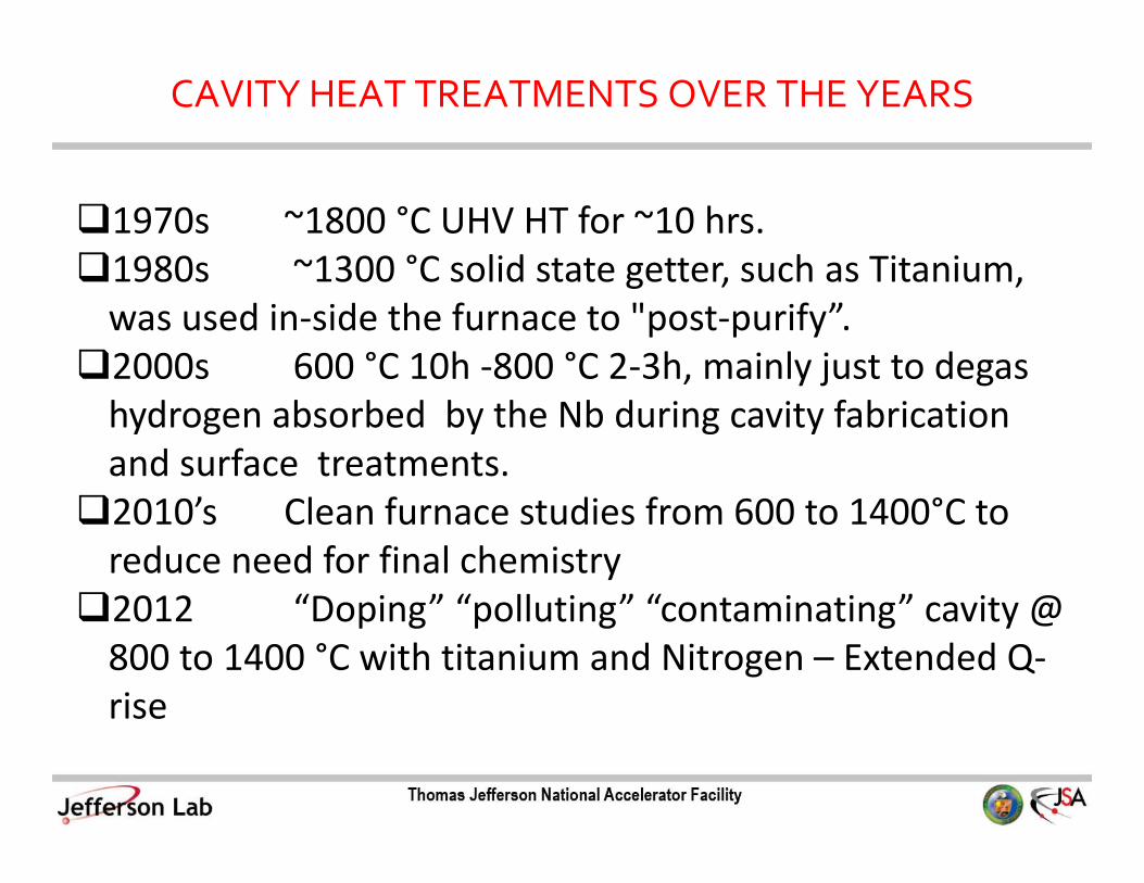
1970s ~1800 °C UHV HT for ~10 hrs. 1980s ~1300 °C solid state getter, such as Titanium, was used in‐side the furnace to "post‐purify”. 2000s 600 °C 10h ‐800 °C 2‐3h, mainly just to degas hydrogen absorbed by the Nb during cavity fabrication and surface treatments. 2010’s Clean furnace studies from 600 to 1400°C to reduce need for final chemistry 2012 “Doping” “polluting” “contaminating” cavity @ 800 to 1400 °C with titanium and Nitrogen – Extended Q‐rise
CAVITY HEAT TREATMENTS OVER THE YEARS

High‐Q0 by Ti doping during furnace treatment
A new induction furnace was designed and installed at JLab to continue the high‐temperature annealing study above 800 °C in a “clean” environment and without subsequent chemistry.
In 2012, heat treatment at 1400°C/3h of an ingot Nb cavity with NbTi flanges at JLab resulted in doping of the surface with Ti (~1 at./%, ~1 mm deep) producing an unprecedented high Q0 ≅ 4.5×10¹⁰ at 2 K, 90 mT
Anne‐Marie Valente‐Feliciano ‐Alternative Surface Preparation ‐USPAS June2015 ‐ Rutgers
Ingot Nb cavity, 1.48 GHz, 2.0 K
P. Dhakal, Rev. Sci. Inst. 83, 065105 (2012) P. Dhakal et al., Phys. Rev. ST Accel. Beams 16, 042001 (2013) P. Dhakal et al., IPAC’14, p. 2651
Avg. Q0(2K) at 19 MV/m measured in VT of C100 cavities
Samples analysis after 1400°C show: Reduced H
content and ~1 at.% Ti content
Higher energy gap and reduced broadening parameter

Nitrogen doping: a breakthrough in Q0
Anne‐Marie Valente‐Feliciano ‐Alternative Surface Preparation ‐USPAS June2015 ‐ Rutgers
2009 JLab attempted to make aHydrogen blocking niobium nitridelayer on the surface of a cavity(purposed in the 1970’s), with nopost heat treatment chemistry.Limited to 1e‐4 torr because ofinterlock so higher pressures neverused. ~30% gain in Q0 (notdoping).
2013 an attempt was made atFNAL to create niobium nitride(Tc=NbN) on the surface of the SRFcavity with nitrogen @ ~20mTorrand 800 °C. The experiment failed.Q = 1e7. But after random materialremoval ,cavity showed new Q‐risenot seem before (except with Tidoping the year before) .
G. Coivati et al., PRST ‐ ACCELERATORS AND BEAMS 13, 022002 (2010)
0 5 10 15 20 25 30 35 40109
1010
1011
Q0
Eacc (MV/m)
T= 2K
Record after nitrogen doping – up to 4 times higher Q!
A. Grassellino et al, 2013 Supercond. Sci. Technol. 26 102001
1.3 GHz
Standard state‐of‐the art preparation: EP+ low T‐baking

Doping treatmentsmall variation from standard XFEL/ILC processing recipe
Example from N20/A30 doping process:
• Light BCP(internal) & Bulk EP (120)• 800 ° C for 3 hours in vacuum• Nitrogen @ 26 mTorr & 800 ° C (diffusion)• 800 °C for 30 minutes in vacuum• Vacuum cooling• 16 µm EP
Cavity after Equator Welding
EP 140 um
Ethanol Rinse
External 20 um BCP
Short HPR
800C HT Bake
RF Tuning
EP 40 um
Ethanol Rinse
Long HPR
Final Assembly
Long HPR
Helium Tank Welding Procedure
VT Assembly
HPR
HOM Tuning
Ship to DESY
Leak Check
120C bake
XFEL
X
X
Courtesy Anna Grassellino FNALX
Anne‐Marie Valente‐Feliciano ‐Alternative Surface Preparation ‐USPAS June2015 ‐ Rutgers

N surface doping : SIMS results
Anne‐Marie Valente‐Feliciano ‐Alternative Surface Preparation ‐USPAS June2015 ‐ Rutgers
A. Romanenko, FNAL, LINAC 2014D. Gonella, Cornell, LINAC 2014

Anne‐Marie Valente‐Feliciano ‐Alternative Surface Preparation ‐USPAS June2015 ‐ Rutgers
Depth Profiling of N for with /without doping Nb Sample under 800˚C Heat‐treatment and EP Removal
1.0E+18
1.0E+19
1.0E+20
1.0E+21
0 50 100 150 200 250 300
NbN
Con
centratio
n (cm^‐3)
Depth (nm)
Depth profile of N ofwith 1 minute N2 doping at ~26 mTorr
vs. without doping samples under 800°C then with 5 µm EP removal
1N/10+50N/10+5
The short‐hand notation 1N/10+5denotes:1. 1minute exposure to ~ 26
mTorr N2 @ 800 °C2. 10minute 800°C vacuum
annealing3. 5 µm electropolish
N concentration drops to around 2~3×10¹⁹ level in less 1µm removal, and remains constant forup to 35 µm removal incrementally by EP for all measured N doped fine grain Nb samples(doping time, different annealing time). Nb samples having same heat‐treatment without Ndoping show 3~5×10¹⁸ level of NbN (detection limit of TOF SIMS for NbN).
N surface doping : SIMS results

N surface doping : Improvements in Q
Anne‐Marie Valente‐Feliciano ‐Alternative Surface Preparation ‐USPAS June2015 ‐ Rutgers
All cavities were Q‐slope limited, with AES035 also having some FE but not enough to limit the test
BASELINE RF TESTS AFTER BULK ELECTRO‐POLISH RESET
All cavities were tested with Stainless steel flanges which add 1.4 nΩ. Residual resistance with 1.4 nΩ has been subtracted from the
data. –
NITROGEN DOPING ROUND 2 RF RESULTS
Courtesy A. Palczewski JLab
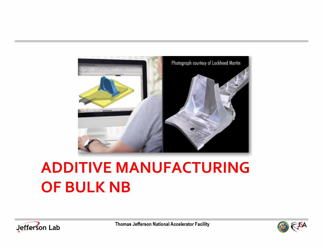
ADDITIVE MANUFACTURING OF BULK NB

Bulk Nb Additive Manufacturing (3D Printing)
Anne‐Marie Valente‐Feliciano ‐ Alternative Surface Preparation ‐ USPAS June2015 ‐ Rutgers
Electron Beam Additive Manufacturing (EBAM) Technology
Additive manufacturing techniques allow for higher average power and otherwise impossible designs
Layers of atomized metal powder /wire is selectively melted with an electron beamUS Patent 7,411,361: Method
and apparatus for radio frequency cavity;
Joint patent with JLab ‐pending: Additive
Manufacturing Method for SRF Components of Various
Geometries
An electron beam melts each layer to a geometry defined by a CAD model
Fully‐dense, functional parts Advantages: Cost/time savings Excellent material properties Added freedom in design
Allows for nearly monolithic, seamless, and thermally‐stabilized SRF niobium structures of arbitrary shape at reduced cost

Bulk Nb Additive Manufacturing
Anne‐Marie Valente‐Feliciano ‐ Alternative Surface Preparation ‐ USPAS June2015 ‐ Rutgers
Electron Beam Melting (ARCAM) 4kW Electron beam is generated within the electron beam
gun The tungsten filament is heated at extremely high
temperatures which releases electrons Electrons accelerate with an electrical field and are focused
by electromagnetic coils The electron beam melts each layer of metal powder to the
desired geometry Vacuum/melt process eliminates impurities and yields high
strength properties of the material Vacuum also facilitates the use of highly reactive metals High build temperature provides good form stability and
low residual stress in the part 20‐200 micron layer thickness 20‐300 micron powder

Bulk Nb Additive Manufacturing
Anne‐Marie Valente‐Feliciano ‐ Alternative Surface Preparation ‐ USPAS June2015 ‐ Rutgers
Fabricating Copper Components with Electron Beam Melting, Advanced Materials & Processes, Vol. 172, Iss. 7, July 2014 (ASM International) C. Terrazas t. al., EBM Fabrication and Characterization of Reactor‐Grade Niobium for Superconductor Applications, Proceeding of Solid Freeform Fabrication Symposium, UT Austin, August 4‐5, 2014 C. Terrazas, Characterization of High‐Purity Niobium Structures Fabricated using the Electron Beam Melting Process ,PhD Dissertation, UT El Paso, August, 2014
RRR measurements (4‐probe method, JLab) showUniform superconducting properties Tc ~ 9.1 to 9.2 K, with sharp transitions As‐EBM, RRR ~ 17‐18 (roughly half of feedstock material) RRR ~ 44 after BCP dip +800˚ C 3hr HV in Ti box

Concluding Remarks
Anne‐Marie Valente‐Feliciano ‐ Alternative Surface Preparation ‐ USPAS June2015 ‐ Rutgers
Non‐exhaustive review of alternative processes for bulk Nb (
Although Bulk Nb has been progressing for the past 40+ yearsand SRF performance is approaching the limit of Nb, there issome room for improvement as shown from the results ofsurface doping with N and Ti.
With the advances in technology in other fields, manufacturing(additive manufacturing) and processing ( ionic liquids, non‐HFchemistry, plasma etching, ALD… ) can be made cheaper, safer(personnel & environment) and more reliable.