Using the UCC28704EVM-724 10-W USB Adapter · Using the UCC28704EVM-724 10-W ... 1 Description The...
21
Using the UCC28704EVM-724 10-W USB Adapter User's Guide Literature Number: SLUUBF1 February 2016
-
Upload
vuongthuan -
Category
Documents
-
view
215 -
download
1
Transcript of Using the UCC28704EVM-724 10-W USB Adapter · Using the UCC28704EVM-724 10-W ... 1 Description The...
Using the UCC28704EVM-724 10-W USBAdapter
User's Guide
Literature Number: SLUUBF1February 2016

www.ti.com
2 SLUUBF1–February 2016Submit Documentation Feedback
Copyright © 2016, Texas Instruments Incorporated
WARNING
Always follow TI’s set-up and application instructions, including use of all interface components within theirrecommended electrical rated voltage and power limits. Always use electrical safety precautions to helpensure your personal safety and the safety of those working around you. Contact TI’s Product InformationCenter http://support/ti./com for further information.
Save all warnings and instructions for future reference.Failure to follow warnings and instructions may result in personal injury, property damage, ordeath due to electrical shock and/or burn hazards.The term TI HV EVM refers to an electronic device typically provided as an open framed, unenclosedprinted circuit board assembly. It is intended strictly for use in development laboratory environments,solely for qualified professional users having training, expertise, and knowledge of electrical safety risks indevelopment and application of high-voltage electrical circuits. Any other use and/or application are strictlyprohibited by Texas Instruments. If you are not suitably qualified, you should immediately stop from furtheruse of the HV EVM.1. Work Area Safety:
(a) Keep work area clean and orderly.(b) Qualified observer(s) must be present anytime circuits are energized.(c) Effective barriers and signage must be present in the area where the TI HV EVM and its interface
electronics are energized, indicating operation of accessible high voltages may be present, for thepurpose of protecting inadvertent access.
(d) All interface circuits, power supplies, evaluation modules, instruments, meters, scopes and otherrelated apparatus used in a development environment exceeding 50 VRMS/75 VDC must beelectrically located within a protected Emergency Power Off (EPO) protected power strip.
(e) Use a stable and non-conductive work surface.(f) Use adequately insulated clamps and wires to attach measurement probes and instruments. No
freehand testing whenever possible.2. Electrical Safety:
(a) De-energize the TI HV EVM and all its inputs, outputs, and electrical loads before performing anyelectrical or other diagnostic measurements. Revalidate that TI HV EVM power has been safely de-energized.
(b) With the EVM confirmed de-energized, proceed with required electrical circuit configurations, wiring,measurement equipment hook-ups and other application needs, while still assuming the EVM circuitand measuring instruments are electrically live.
(c) Once EVM readiness is complete, energize the EVM as intended.
WARNING: while the EVM is energized, never touch the EVM or its electrical circuits as theycould be at high voltages capable of causing electrical shock hazard.
3. Personal Safety:(a) Wear personal protective equipment e.g. latex gloves and/or safety glasses with side shields or
protect EVM in an adequate lucent plastic box with interlocks from accidental touch.4. Limitation for Safe Use:
(a) EVMs are not to be used as all or part of a production unit.

3SLUUBF1–February 2016Submit Documentation Feedback
Copyright © 2016, Texas Instruments Incorporated
Using the UCC28704EVM-724 10-W USB Adapter
User's GuideSLUUBF1–February 2016
Using the UCC28704EVM-724 10-W USB Adapter
1 DescriptionThe UCC28704EVM-724 is a 10-W evaluation module for evaluating an off-line adapter for USBapplications. The EVM meets CoC tier 2 and DoE Level 6 efficiency and standby power requirements. It isintended for evaluation purposes and is not intended to be an end product. The UCC28704EVM-724converters 85-VRMS to 265-VRMS input voltage down to 5-VDC, with a 2.1-A current limit for USB adapterapplications.
Figure 1. UCC28704EVM-724

Electrical Performance Specifications www.ti.com
4 SLUUBF1–February 2016Submit Documentation Feedback
Copyright © 2016, Texas Instruments Incorporated
Using the UCC28704EVM-724 10-W USB Adapter
2 Electrical Performance Specifications
(1) Specification includes loss from 0.15-Ω cable.(2) Specification measured at the end of 1 m of 0.15-Ω cable with 100 nF of filter capacitance.
Table 1. UCC28704EVM-724 Electrical Performance Specifications
PARAMETER TEST CONDITIONS MIN TYP MAX UNITINPUT CHARACTERISTICSVIN Input voltage (RMS) 85 115/230 265 VfLINE Line frequency 47 50/60 63 HzPSTBY No load input power VIN = 115 V / 230 V RMS, IOUT = 0 A 50 65 mWOUTPUT CHARACTERISTICSVOUT Output voltage (1) VIN = nom, IOUT = nom 4.75 5.25 VVOUT Output ripple voltage (2) VIN = nom, IOUT = max, 80 mVppIOUT Output current VIN = min to max 2 2.2 AIOUT Constant current VIN = min to max 2 2.1 2.2 A
Load step 0 A to 0.5 A 4.1 6 VSYSTEMS CHARACTERISTICS
η 4-point average efficiency 25%, 50%, 75% and 100% load, 115-V / 230-VRMS input 83%
η 4-point average efficiency (1) 25%, 50%, 75% and 100% load, 115-V / 230-VRMS input 80%
η 10% Efficiency 115-V / 230-V RMS input 75% 77%Operating temperaturerange VIN = min to max, IOUT = min to max 25 °C
~3
+1
~4
-2
D1
HD
06
-T
F1
INP
UT:
85
VR
MS
-2
65
VR
MS
,0
.35
AP
EA
K,
47
Hz
TO
63
Hz
SG
ND
SG
ND
10
0p
F
C10
VO
UT
= 5
V @
2A
10
R17
1
32
Q1
ST
U7
NM
60
N
PG
ND
PG
ND
PG
ND
10
µF
C2
1µ
FC
71
.00
kR
9
2.1
5R
15
No
Co
mp
on
en
t V
alu
e =
Un
po
pu
late
d
C9
L N
10
µF
C1
47
0µ
FC
54
70
µF
C6
75
0µ
H
1 2
3 45
6
FL
1
FL2
MH1
MH2
T1
PG
ND
1
3
2
D3
SB
RT
15
U50
SP
5-1
3
NT
C1
VD
D2
VS
6
GN
D5
CS
4
DR
V3
U1
47
0µ
H
L1
5o
hm
t°
RT
1
2.1
5R
16
10
0k
oh
m
t°
RT
20
.33
µF
C8
D4
MU
RS
16
0-1
3-F
5.1
1M
R2
5.1
1M
R3 5
.11
MR
4
0R14
36
.5k
R12
11
5k
R11
D2
MU
RS
16
0-1
3-F
51
.1
R6
47
0p
FC
3
511
kR
5
PG
ND
1.0
0k
R1
TP
1
20
R10
TP
2
TP
3
TP
4
VB
US
1
D-
2
D+
3
GN
D4
S1 S2
J1
L2
R7
C4
71
5
R13
0R18 0R
19
PG
ND
L3
12
J2
www.ti.com Schematic
5SLUUBF1–February 2016Submit Documentation Feedback
Copyright © 2016, Texas Instruments Incorporated
Using the UCC28704EVM-724 10-W USB Adapter
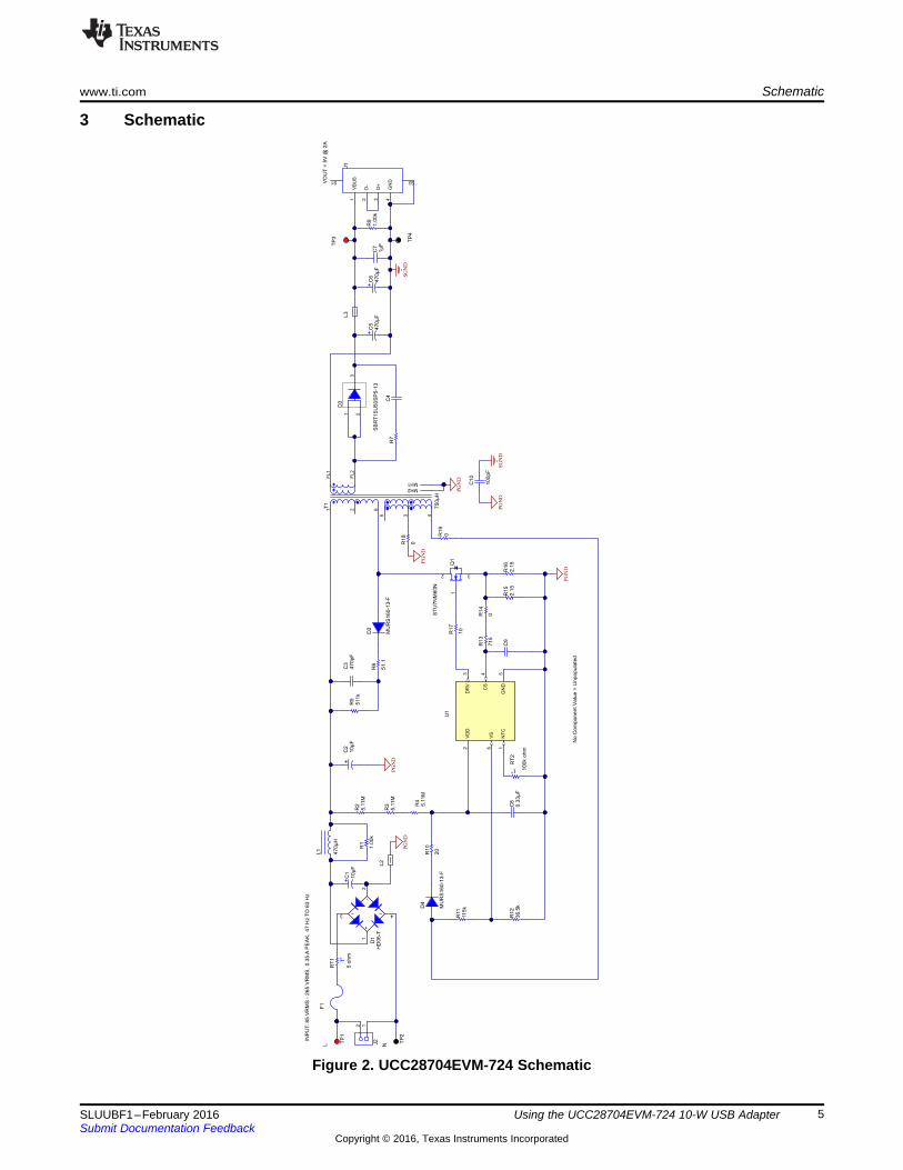
3 Schematic
Figure 2. UCC28704EVM-724 Schematic

AC Line
AC Neutral
VOUT +
VOUTí
Isolated Variable AC Source
1 ��Precision Shunt
CurrentMeasurement
VoltageMeasurement
Power Analyzer
Load
UCC28704EVM-724
TP1
TP2
TP3
TP4
Volt Meter
Oscilloscope
100 nF
Scope Probe
Measuring Standby Power Requires Moving Neutral Sensing for the Power Analyzer
Test Setup www.ti.com
6 SLUUBF1–February 2016Submit Documentation Feedback
Copyright © 2016, Texas Instruments Incorporated
Using the UCC28704EVM-724 10-W USB Adapter
4 Test Setup
4.1 Test Setup RequirementsSafety: This evaluation module is not encapsulated and there are voltages that are much greater than 50VDC.
WARNINGIf you are not trained in the proper safety of handling and testingpower electronics please do not test this evaluation module.
Voltage Source: Isolated AC source or variable AC transformer capable of 265 VAC cable of handling 10W
Voltmeter: Digital voltage meter
Power Analyzer: Capable of measuring 1 mW to 10 W of input power and capable of handling 265-VRMS input voltage. Some power analyzers may require a precision shunt resistor for measuring inputcurrent to measure input power of 5 W or less. Please read the power analyzer’s user manual for propersetup.
Oscilloscope:• 4 Channel 100 MHz.• Probes capable of handling 600 V.
Output Load: Resistive or electronic load capable handling 15 W at 5 V.
Recommended Wire Gauge: Insulated 22 AWG.
4.2 Test Setup Diagram
Figure 3. UCC28704EVM-724 Test Setup Diagram

www.ti.com Test Points
7SLUUBF1–February 2016Submit Documentation Feedback
Copyright © 2016, Texas Instruments Incorporated
Using the UCC28704EVM-724 10-W USB Adapter
5 Test Points
Table 2. Test Point Functions
TEST POINTS NAME DESCRIPTIONTP1 L AC line voltage inputTP2 N AC neutral inputTP3 VOUT + Output supplyTP4 VOUT – Output return
6 Performance Data and Typical Characteristic Curves
6.1 Efficiency
Table 3. Efficiency Test Data
VIN RMS VOUT IOUT PINEFFICIENCYWITH CABLE
EFFICIENCYAVERAGE
WITH CABLE
EFFICIENCYWITHOUT
CABLE
EFFICIENCYAVERAGEWITHOUT
CABLE85 5.120 0.000 0.032 N/A N/A N/A N/A85 5.346 2.003 13.132 77.0% N/A 81.5% N/A265 5.123 0.000 0.055 N/A N/A N/A N/A265 5.346 2.003 12.856 78.6% N/A 83.3% N/A115 5.121 0.000 0.036 N/A N/A N/A115 5.115 0.200 1.267 80.3% 80.7%115 5.154 0.501 3.095 82.2% 83.4%115 5.221 1.001 6.238 81.4% 83.8%115 5.283 1.502 9.495 80.0% 83.6%115 5.348 2.003 12.796 79.0% 80.7% 83.7% 83.6%230 5.122 0.000 0.050 N/A N/A230 5.116 0.200 1.327 76.7% 77.1%230 5.150 0.501 3.152 80.7% 81.9%230 5.214 1.001 6.241 81.2% 83.6%230 5.281 1.502 9.482 80.1% 83.7%230 5.334 2.003 12.735 79.2% 80.3% 83.9% 83.3%

IOUT
VO
UT
0.00
00.
100
0.20
00.
300
0.40
00.
500
0.60
00.
700
0.80
00.
900
1.00
01.
100
1.20
01.
300
1.40
01.
500
1.60
01.
700
1.80
01.
900
2.00
02.
100
2.20
0
2.000
2.500
3.000
3.500
4.000
4.500
5.000
5.500
D002
VOUT @ 115 VRMSVOUT @ 115 VRMS With Cable
IOUT
VO
UT
0.00
00.
100
0.20
00.
300
0.40
00.
500
0.60
00.
700
0.80
00.
900
1.00
01.
100
1.20
01.
300
1.40
01.
500
1.60
01.
700
1.80
01.
900
2.00
02.
100
2.20
02.000
2.500
3.000
3.500
4.000
4.500
5.000
5.500
D003
VOUT @ 230 VRMSVOUT @ 230 VRMS With Cable
Output Power
% E
ffici
ency
10% 20% 30% 40% 50% 60% 70% 80% 90% 100%60.0%
65.0%
70.0%
75.0%
80.0%
85.0%
D001
Efficiency Without Cable @ 115 VRMSEfficiency Without Cable @ 230 VRMSEfficiency With 0.15-: Cable @ 115 VRMSEfficiency With 0.15-: Cable @ 230 VRMS
Performance Data and Typical Characteristic Curves www.ti.com
8 SLUUBF1–February 2016Submit Documentation Feedback
Copyright © 2016, Texas Instruments Incorporated
Using the UCC28704EVM-724 10-W USB Adapter
Figure 4. Efficency
6.2 VI Characteristics
Figure 5. VIN = 115 VRMS Figure 6. VIN = 230 VRMS

VVDD
VOUT
Aux
VRCS
VIN
VOUT
Aux
VRCS
www.ti.com Performance Data and Typical Characteristic Curves
9SLUUBF1–February 2016Submit Documentation Feedback
Copyright © 2016, Texas Instruments Incorporated
Using the UCC28704EVM-724 10-W USB Adapter
6.3 StartupCH1 = Aux (D4 Anode), CH2 = VOUT, CH3 = VRCS (R16) , CH4 = VIN (C1), RLOAD = 2.5 Ω
CH1 = 100 V/div, CH2 = 5 V/div, CH3 = 1 V/div, CH4 = 200 V/div
Figure 7. VIN = 85 VRMSFigure 8. VIN = 265 VRMS
CH1 = Aux (D4 Anode), CH2 = VOUT, CH3 = VRCS (R16) , CH4 = VVDD (C8)
CH1 = 100 V/div, CH2 = 2 V/div, CH3 = 1 V/div, CH4 = 20 V/div
Figure 9. VIN = 115 VRMS, Unloaded Figure 10. VIN = 115 VRMS, 2.5-Ω Load
Figure 11. VIN = 230 VRMS, Unloaded Figure 12. VIN = 230 VRMS, 2.5-Ω Load

V = 5.528 V to 4.520 VOUT
VOUT
Aux
VRCS
IOUT
Performance Data and Typical Characteristic Curves www.ti.com
10 SLUUBF1–February 2016Submit Documentation Feedback
Copyright © 2016, Texas Instruments Incorporated
Using the UCC28704EVM-724 10-W USB Adapter
6.4 Load TransientsCH1 = Aux (D4 Anode), CH2 = VOUT, CH3 = VRCS (R16), CH4 = IOUT
CH1 = 100 V/div, CH2 = 1 V/div, CH3 = 2 V/div, CH4 = 2 A/div
Load = 0 to 2 A, 50 Hz, 50% Duty Cycle
Figure 13. VIN = 85 V RMS Figure 14. VIN = 115 V RMS
Figure 15. VIN = 230 V RMS Figure 16. VIN = 265 V RMS
6.5 Output Ripple Voltage at Full LoadCH1 = VOUT at EVM output, CH2 = VOUT measured at the end of the 3 m of cable in parallel with a 100-nF capacitor. The output voltage has less than 80 mV of output ripple at the end of the cable.
Figure 17. VIN = 85 VRMS, IOUT = 2 A Figure 18. VIN = 265 VRMS, IOUT = 2 A

VVDD
VOUT
Aux
VRCS
VQ1d
Aux
VRCS
www.ti.com Performance Data and Typical Characteristic Curves
11SLUUBF1–February 2016Submit Documentation Feedback
Copyright © 2016, Texas Instruments Incorporated
Using the UCC28704EVM-724 10-W USB Adapter
6.6 Q1 Drain Voltage EvaluationCH1 = Aux (D4 Anode), CH3 = VRCS (R15), CH3 = Q1d
CH1 = 100 V/div, CH3 = 1 V/div, CH4 = 200 V/div
Figure 19. VIN = 85 VRMS, IOUT = 2 A Figure 20. VIN = 265 VRMS
6.7 Constant Current Under Voltage ProtectionThe UCC28704 has constant current under voltage protection (CCUV) that can be used to protect theconverter from excessive loading for long periods of time. When the output is pulled bellow 2.95 V forgreater than 120 ms in this design the UCC28704 activates CCUV protection. The converter will stopswitching and charge and discharge the VDD capacitor (C8) 4 times between ULVO turn on and turnoffbefore trying to restart the adapter. After VDD reaches the UCC28704 UVLO turn on threshold it will thenattempt to restart. If the fault condition remains the UCC28704 will enter the fault condition again and willrepeat the cycling of the VDD capacitor until the fault is cleared. Please refer to the UCC28704 data sheetfor more details. The waveform in Figure 21 show this CCUV fault behavior with the output loaded with a2.9-V constant voltage load briefly.
CH1 = VVDD, CH2 = VOUT, CH3 = VRCS (R16), CH4 = Aux (D4 Anode)
CH1 = 10 V/div, CH2 = 2 V/div, CH3 = 2 V/div, CH4 = 100 V/div
Figure 21. CCUV Fault Behavior

Performance Data and Typical Characteristic Curves www.ti.com
12 SLUUBF1–February 2016Submit Documentation Feedback
Copyright © 2016, Texas Instruments Incorporated
Using the UCC28704EVM-724 10-W USB Adapter
6.8 Conducted EMI Output Grounded to LISN ground
Figure 22. VIN = 115 VRMS, Load = 2.5 Ω Figure 23. VIN = 115 VRMS, Load = 2.5 Ω
NOTE: Please note this was evaluated on an unqualified EMI station. It is recommended that allfinal designs be verified by agency qualified EMI test house.

1
2
6
Np/2
Np/2
4
3
Na1 Na2
5
Nc1 Nc2
Ns1 Ns2
FL1
FL2
Flying Leads (FL)
www.ti.com Transformer Details
13SLUUBF1–February 2016Submit Documentation Feedback
Copyright © 2016, Texas Instruments Incorporated
Using the UCC28704EVM-724 10-W USB Adapter
7 Transformer DetailsWurth Elektronik transformer part number 750315841 is used on this design and wound on an RM6 core.
Figure 24. Transformer Schematic
Table 4. Transformer Specifications
PARAMETER PINS/LEADS TEST CONDITIONS VALUED.C. resistance 1 – 2 At 20ºC 0.56 Ω, ±10%D.C. resistance 3 – 4 At 20ºC 0.157 Ω, ±10%D.C. resistance FL1 – FL2 At 20ºC 0.012 Ω, ±20%D.C. resistance 3 – 5 At 20ºC 0.142 Ω, ±10%D.C. resistance 2 – 6 At 20ºC 0.845 Ω, ±10%
Inductance 1 – 6 10 kHz, 100 mV, Ls 750 µH, ±10%Saturation current 1 – 6 20% rolloff from initial 800 mA
Leakage inductance 1 – 6 tie (FL1 + FL2, 3 + 4 + 5),100kHz, 100 mV, Ls
4.0 µH typical, 6.0 µHmaximum
Dielectric 6vFL1 tie (5 + 6), 3750 VAC, 1 secondTurns ratio (1 – 6):(FL1 – FL2) 13:1, ±1%Turns ratio (1 – 6):(3 – 4) 4:1, ±1%Turns ratio (1 – 6):(5 – 3) 5.78:1, ±1%Turns ratio (1 – 2):(2 – 6) 1:1, ±1%

1
2
Tape
Nc1 = 9 turns, 34 AWG
Nc2 = 9 turns, 34 AWG
Wound Bifilar Single Layer 5
Tape
Tape
Na1 = 13 turns, 34 AWG
Na2 = 13 turns 34 AWG
Wound Bifilar Single Layer
3 4
Tape
Np/2 = 26 Turns, 34 AWG, Single Layer 2
Bobbin Surface
Transformer Inner Core
Clockwise
Clockwise
Ns1 = 4 turns, 25 AWG Triple Insulated
Ns2 = 4 turns, 25 AWG Triple Insulated
Wound Bifilar Single Layer
FL1 FL2 Clockwise
3Counter
Clockwise
Np/2 = 26 Turns, 34 AWG
20 Turns on one layer and 6 on the next6 Clockwise
PinPin
Start Winding Finish Winding
Winding Direction
Transformer Outer Core
Transformer Details www.ti.com
14 SLUUBF1–February 2016Submit Documentation Feedback
Copyright © 2016, Texas Instruments Incorporated
Using the UCC28704EVM-724 10-W USB Adapter
Figure 25. Transformer Winding Structure

J2
Q1
www.ti.com EVM Assembly and Layout
15SLUUBF1–February 2016Submit Documentation Feedback
Copyright © 2016, Texas Instruments Incorporated
Using the UCC28704EVM-724 10-W USB Adapter
8 EVM Assembly and Layout
Figure 26. EVM Assembly (Top View)
Figure 27. EVM Assembly/Layout (Bottom View)

List of Materials www.ti.com
16 SLUUBF1–February 2016Submit Documentation Feedback
Copyright © 2016, Texas Instruments Incorporated
Using the UCC28704EVM-724 10-W USB Adapter
9 List of MaterialsUCC28704EVM-724 list of materials as shown in Figure 2.
Table 5. UCC28704EVM-724 List of Materials
Quantity Designator Description PartNumber Manufacturer
2 C1, C2 Capacitor, aluminum, 10 µF, 400 V, ±20%, TH UCS2G100MPD1TD Nichicon1 C3 Capacitor, ceramic, 470 pF, 630 V, ± 5%, U2J, 1206 GRM31A7U2J471JW31D MuRata0 C4 Capacitor, ceramic, 100 pF, 50 V, ±5%, C0G/NP0,
080508055A101JAT2A AVX
2 C5, C6 Capacitor, aluminum, 470 µF, 16 V, ±20%, 0.009 ohm,TH
PLF1C471MDO1 Nichicon
1 C7 Capacitor, ceramic, 1 µF, 25 V, ±10%, X7R, 0603 C1608X7R1E105K080AB TDK1 C8 Capacitor, ceramic, 0.33 µF, 50 V, ±10%, X7R, 1206 GRM319R71H334KA01D MuRata0 C9 Capacitor, ceramic, 27 pF, 50 V, ±5%, C0G/NP0, 0603 06035A270JAT2A AVX1 C10 Capacitor, ceramic, 100 pF, 440 V, ±10%, B, 7.0 mm ×
11.0 mm × 7.0 mmCD70-B2GA101KYNKA TDK
1 D1 Diode, switching-bridge, 600 V, 0.8 A, MiniDIP HD06-T Diodes Inc.2 D2, D4 Diode, ultrafast, 600 V, 1 A, SMB MURS160-13-F Diodes Inc.1 D3 Diode, super barrier rectifier, 50 V, 15 A, AEC-Q101,
PowerDI5SBRT15U50SP5-13 Diodes Inc.
1 F1 Fuse, 0.5 A, 250 VAC/VDC, TH RST 500 Bel Fuse1 J1 Connector, receptacle, USB type A, vertical, TH 923 Keystone1 J2 2 pos terminal block 1715721 Phoenix Contact1 L1 Inductor, wirewound, ferrite, 470 µH, 0.5 A, 1.3 Ω, TH RLB0914-471KL Bourns2 L2, L3 Ferrite bead, 300 Ω at 100 MHz, 3 A, 1206_190 742792121 Wurth Elektronik1 Q1 MOSFET, N-channel, 600 V, 5 A, IPAK STU7NM60N STMicroelectronics1 R1 Resistor, 1.00 kΩ, 1%, 0.25 W, 1206 CRCW12061K00FKEA Vishay-Dale3 R2, R3,
R4Resistor, 5.11 MΩ, 1%, 0.125 W, 0805 CRCW08055M11FKEA Vishay-Dale
1 R5 Resistor, 511 kΩ, 1%, 0.25 W, 1206 CRCW1206511KFKEA Vishay-Dale1 R6 Resistor, 51.1, 1%, 0.125 W, 0805 CRCW080551R1FKEA Vishay-Dale0 R7 Resistor, 510 kΩ, 5%, 0.125 W, 0805 CRCW0805510KJNEA Vishay-Dale1 R9 Resistor, 1.00 kΩ, 1%, 0.1 W, 0603 CRCW06031K00FKEA Vishay-Dale1 R10 Resistor, 20 Ω, 5%, 0.125 W, 0805 CRCW080520R0JNEA Vishay-Dale1 R11 Resistor, 115 kΩ, 1%, 0.125 W, 0805 CRCW0805115KFKEA Vishay-Dale1 R12 Resistor, 36.5 kΩ, 1%, 0.1 W, 0603 CRCW060336K5FKEA Vishay-Dale1 R13 Resistor, 715 Ω, 1%, 0.1 W, 0603 RC0603FR-07715RL Yageo America3 R14, R18,
R19Resistor, 0 Ω, 5%, 0.25 W, 1206 MCR18EZHJ000 Rohm
2 R15, R16 Resistor, 2.15 Ω, 1%, 0.125 W, 0805 CRCW08052R15FKEA Vishay-Dale1 R17 Resistor, 10 Ω, 5%, 0.25 W, 0603 CRCW060310R0JNEAHP Vishay-Dale1 RT1 Thermistor NTC, 5 Ω, 20%, MF72D5 TH MF72-005D5 Cantherm1 RT2 Thermistor NTC, 100 kΩ, 1%, 0603 NTCG164KF104F TDK1 T1 Transformer, 750 µH, TH 750315841 Wurth Elektronik2 TP1, TP3 Test point, multipurpose, red, TH 5010 Keystone2 TP2, TP4 Test point, multipurpose, black, TH 5011 Keystone1 U1 CV/CC Flyback Controller with Primary-Side Regulation
(PSR) and CC Under-Voltage Protection, DBV0006AUCC28704DBVR-1 Texas Instruments

STANDARD TERMS AND CONDITIONS FOR EVALUATION MODULES1. Delivery: TI delivers TI evaluation boards, kits, or modules, including any accompanying demonstration software, components, or
documentation (collectively, an “EVM” or “EVMs”) to the User (“User”) in accordance with the terms and conditions set forth herein.Acceptance of the EVM is expressly subject to the following terms and conditions.1.1 EVMs are intended solely for product or software developers for use in a research and development setting to facilitate feasibility
evaluation, experimentation, or scientific analysis of TI semiconductors products. EVMs have no direct function and are notfinished products. EVMs shall not be directly or indirectly assembled as a part or subassembly in any finished product. Forclarification, any software or software tools provided with the EVM (“Software”) shall not be subject to the terms and conditionsset forth herein but rather shall be subject to the applicable terms and conditions that accompany such Software
1.2 EVMs are not intended for consumer or household use. EVMs may not be sold, sublicensed, leased, rented, loaned, assigned,or otherwise distributed for commercial purposes by Users, in whole or in part, or used in any finished product or productionsystem.
2 Limited Warranty and Related Remedies/Disclaimers:2.1 These terms and conditions do not apply to Software. The warranty, if any, for Software is covered in the applicable Software
License Agreement.2.2 TI warrants that the TI EVM will conform to TI's published specifications for ninety (90) days after the date TI delivers such EVM
to User. Notwithstanding the foregoing, TI shall not be liable for any defects that are caused by neglect, misuse or mistreatmentby an entity other than TI, including improper installation or testing, or for any EVMs that have been altered or modified in anyway by an entity other than TI. Moreover, TI shall not be liable for any defects that result from User's design, specifications orinstructions for such EVMs. Testing and other quality control techniques are used to the extent TI deems necessary or asmandated by government requirements. TI does not test all parameters of each EVM.
2.3 If any EVM fails to conform to the warranty set forth above, TI's sole liability shall be at its option to repair or replace such EVM,or credit User's account for such EVM. TI's liability under this warranty shall be limited to EVMs that are returned during thewarranty period to the address designated by TI and that are determined by TI not to conform to such warranty. If TI elects torepair or replace such EVM, TI shall have a reasonable time to repair such EVM or provide replacements. Repaired EVMs shallbe warranted for the remainder of the original warranty period. Replaced EVMs shall be warranted for a new full ninety (90) daywarranty period.
3 Regulatory Notices:3.1 United States
3.1.1 Notice applicable to EVMs not FCC-Approved:This kit is designed to allow product developers to evaluate electronic components, circuitry, or software associated with the kitto determine whether to incorporate such items in a finished product and software developers to write software applications foruse with the end product. This kit is not a finished product and when assembled may not be resold or otherwise marketed unlessall required FCC equipment authorizations are first obtained. Operation is subject to the condition that this product not causeharmful interference to licensed radio stations and that this product accept harmful interference. Unless the assembled kit isdesigned to operate under part 15, part 18 or part 95 of this chapter, the operator of the kit must operate under the authority ofan FCC license holder or must secure an experimental authorization under part 5 of this chapter.3.1.2 For EVMs annotated as FCC – FEDERAL COMMUNICATIONS COMMISSION Part 15 Compliant:
CAUTIONThis device complies with part 15 of the FCC Rules. Operation is subject to the following two conditions: (1) This device may notcause harmful interference, and (2) this device must accept any interference received, including interference that may causeundesired operation.Changes or modifications not expressly approved by the party responsible for compliance could void the user's authority tooperate the equipment.
FCC Interference Statement for Class A EVM devicesNOTE: This equipment has been tested and found to comply with the limits for a Class A digital device, pursuant to part 15 ofthe FCC Rules. These limits are designed to provide reasonable protection against harmful interference when the equipment isoperated in a commercial environment. This equipment generates, uses, and can radiate radio frequency energy and, if notinstalled and used in accordance with the instruction manual, may cause harmful interference to radio communications.Operation of this equipment in a residential area is likely to cause harmful interference in which case the user will be required tocorrect the interference at his own expense.
SPACER
SPACER
SPACER
SPACER
SPACER
SPACER
SPACER
SPACER

FCC Interference Statement for Class B EVM devicesNOTE: This equipment has been tested and found to comply with the limits for a Class B digital device, pursuant to part 15 ofthe FCC Rules. These limits are designed to provide reasonable protection against harmful interference in a residentialinstallation. This equipment generates, uses and can radiate radio frequency energy and, if not installed and used in accordancewith the instructions, may cause harmful interference to radio communications. However, there is no guarantee that interferencewill not occur in a particular installation. If this equipment does cause harmful interference to radio or television reception, whichcan be determined by turning the equipment off and on, the user is encouraged to try to correct the interference by one or moreof the following measures:
• Reorient or relocate the receiving antenna.• Increase the separation between the equipment and receiver.• Connect the equipment into an outlet on a circuit different from that to which the receiver is connected.• Consult the dealer or an experienced radio/TV technician for help.
3.2 Canada3.2.1 For EVMs issued with an Industry Canada Certificate of Conformance to RSS-210
Concerning EVMs Including Radio Transmitters:This device complies with Industry Canada license-exempt RSS standard(s). Operation is subject to the following two conditions:(1) this device may not cause interference, and (2) this device must accept any interference, including interference that maycause undesired operation of the device.
Concernant les EVMs avec appareils radio:Le présent appareil est conforme aux CNR d'Industrie Canada applicables aux appareils radio exempts de licence. L'exploitationest autorisée aux deux conditions suivantes: (1) l'appareil ne doit pas produire de brouillage, et (2) l'utilisateur de l'appareil doitaccepter tout brouillage radioélectrique subi, même si le brouillage est susceptible d'en compromettre le fonctionnement.
Concerning EVMs Including Detachable Antennas:Under Industry Canada regulations, this radio transmitter may only operate using an antenna of a type and maximum (or lesser)gain approved for the transmitter by Industry Canada. To reduce potential radio interference to other users, the antenna typeand its gain should be so chosen that the equivalent isotropically radiated power (e.i.r.p.) is not more than that necessary forsuccessful communication. This radio transmitter has been approved by Industry Canada to operate with the antenna typeslisted in the user guide with the maximum permissible gain and required antenna impedance for each antenna type indicated.Antenna types not included in this list, having a gain greater than the maximum gain indicated for that type, are strictly prohibitedfor use with this device.
Concernant les EVMs avec antennes détachablesConformément à la réglementation d'Industrie Canada, le présent émetteur radio peut fonctionner avec une antenne d'un type etd'un gain maximal (ou inférieur) approuvé pour l'émetteur par Industrie Canada. Dans le but de réduire les risques de brouillageradioélectrique à l'intention des autres utilisateurs, il faut choisir le type d'antenne et son gain de sorte que la puissance isotroperayonnée équivalente (p.i.r.e.) ne dépasse pas l'intensité nécessaire à l'établissement d'une communication satisfaisante. Leprésent émetteur radio a été approuvé par Industrie Canada pour fonctionner avec les types d'antenne énumérés dans lemanuel d’usage et ayant un gain admissible maximal et l'impédance requise pour chaque type d'antenne. Les types d'antennenon inclus dans cette liste, ou dont le gain est supérieur au gain maximal indiqué, sont strictement interdits pour l'exploitation del'émetteur
3.3 Japan3.3.1 Notice for EVMs delivered in Japan: Please see http://www.tij.co.jp/lsds/ti_ja/general/eStore/notice_01.page 日本国内に
輸入される評価用キット、ボードについては、次のところをご覧ください。http://www.tij.co.jp/lsds/ti_ja/general/eStore/notice_01.page
3.3.2 Notice for Users of EVMs Considered “Radio Frequency Products” in Japan: EVMs entering Japan may not be certifiedby TI as conforming to Technical Regulations of Radio Law of Japan.
If User uses EVMs in Japan, not certified to Technical Regulations of Radio Law of Japan, User is required by Radio Law ofJapan to follow the instructions below with respect to EVMs:1. Use EVMs in a shielded room or any other test facility as defined in the notification #173 issued by Ministry of Internal
Affairs and Communications on March 28, 2006, based on Sub-section 1.1 of Article 6 of the Ministry’s Rule forEnforcement of Radio Law of Japan,
2. Use EVMs only after User obtains the license of Test Radio Station as provided in Radio Law of Japan with respect toEVMs, or
3. Use of EVMs only after User obtains the Technical Regulations Conformity Certification as provided in Radio Law of Japanwith respect to EVMs. Also, do not transfer EVMs, unless User gives the same notice above to the transferee. Please notethat if User does not follow the instructions above, User will be subject to penalties of Radio Law of Japan.
SPACER
SPACER
SPACER
SPACER
SPACER

【無線電波を送信する製品の開発キットをお使いになる際の注意事項】 開発キットの中には技術基準適合証明を受けていないものがあります。 技術適合証明を受けていないもののご使用に際しては、電波法遵守のため、以下のいずれかの措置を取っていただく必要がありますのでご注意ください。1. 電波法施行規則第6条第1項第1号に基づく平成18年3月28日総務省告示第173号で定められた電波暗室等の試験設備でご使用
いただく。2. 実験局の免許を取得後ご使用いただく。3. 技術基準適合証明を取得後ご使用いただく。
なお、本製品は、上記の「ご使用にあたっての注意」を譲渡先、移転先に通知しない限り、譲渡、移転できないものとします。上記を遵守頂けない場合は、電波法の罰則が適用される可能性があることをご留意ください。 日本テキサス・イ
ンスツルメンツ株式会社東京都新宿区西新宿6丁目24番1号西新宿三井ビル
3.3.3 Notice for EVMs for Power Line Communication: Please see http://www.tij.co.jp/lsds/ti_ja/general/eStore/notice_02.page電力線搬送波通信についての開発キットをお使いになる際の注意事項については、次のところをご覧ください。http://www.tij.co.jp/lsds/ti_ja/general/eStore/notice_02.page
SPACER4 EVM Use Restrictions and Warnings:
4.1 EVMS ARE NOT FOR USE IN FUNCTIONAL SAFETY AND/OR SAFETY CRITICAL EVALUATIONS, INCLUDING BUT NOTLIMITED TO EVALUATIONS OF LIFE SUPPORT APPLICATIONS.
4.2 User must read and apply the user guide and other available documentation provided by TI regarding the EVM prior to handlingor using the EVM, including without limitation any warning or restriction notices. The notices contain important safety informationrelated to, for example, temperatures and voltages.
4.3 Safety-Related Warnings and Restrictions:4.3.1 User shall operate the EVM within TI’s recommended specifications and environmental considerations stated in the user
guide, other available documentation provided by TI, and any other applicable requirements and employ reasonable andcustomary safeguards. Exceeding the specified performance ratings and specifications (including but not limited to inputand output voltage, current, power, and environmental ranges) for the EVM may cause personal injury or death, orproperty damage. If there are questions concerning performance ratings and specifications, User should contact a TIfield representative prior to connecting interface electronics including input power and intended loads. Any loads appliedoutside of the specified output range may also result in unintended and/or inaccurate operation and/or possiblepermanent damage to the EVM and/or interface electronics. Please consult the EVM user guide prior to connecting anyload to the EVM output. If there is uncertainty as to the load specification, please contact a TI field representative.During normal operation, even with the inputs and outputs kept within the specified allowable ranges, some circuitcomponents may have elevated case temperatures. These components include but are not limited to linear regulators,switching transistors, pass transistors, current sense resistors, and heat sinks, which can be identified using theinformation in the associated documentation. When working with the EVM, please be aware that the EVM may becomevery warm.
4.3.2 EVMs are intended solely for use by technically qualified, professional electronics experts who are familiar with thedangers and application risks associated with handling electrical mechanical components, systems, and subsystems.User assumes all responsibility and liability for proper and safe handling and use of the EVM by User or its employees,affiliates, contractors or designees. User assumes all responsibility and liability to ensure that any interfaces (electronicand/or mechanical) between the EVM and any human body are designed with suitable isolation and means to safelylimit accessible leakage currents to minimize the risk of electrical shock hazard. User assumes all responsibility andliability for any improper or unsafe handling or use of the EVM by User or its employees, affiliates, contractors ordesignees.
4.4 User assumes all responsibility and liability to determine whether the EVM is subject to any applicable international, federal,state, or local laws and regulations related to User’s handling and use of the EVM and, if applicable, User assumes allresponsibility and liability for compliance in all respects with such laws and regulations. User assumes all responsibility andliability for proper disposal and recycling of the EVM consistent with all applicable international, federal, state, and localrequirements.
5. Accuracy of Information: To the extent TI provides information on the availability and function of EVMs, TI attempts to be as accurateas possible. However, TI does not warrant the accuracy of EVM descriptions, EVM availability or other information on its websites asaccurate, complete, reliable, current, or error-free.
SPACER
SPACER
SPACER
SPACER
SPACER
SPACER

SPACER6. Disclaimers:
6.1 EXCEPT AS SET FORTH ABOVE, EVMS AND ANY WRITTEN DESIGN MATERIALS PROVIDED WITH THE EVM (AND THEDESIGN OF THE EVM ITSELF) ARE PROVIDED "AS IS" AND "WITH ALL FAULTS." TI DISCLAIMS ALL OTHERWARRANTIES, EXPRESS OR IMPLIED, REGARDING SUCH ITEMS, INCLUDING BUT NOT LIMITED TO ANY IMPLIEDWARRANTIES OF MERCHANTABILITY OR FITNESS FOR A PARTICULAR PURPOSE OR NON-INFRINGEMENT OF ANYTHIRD PARTY PATENTS, COPYRIGHTS, TRADE SECRETS OR OTHER INTELLECTUAL PROPERTY RIGHTS.
6.2 EXCEPT FOR THE LIMITED RIGHT TO USE THE EVM SET FORTH HEREIN, NOTHING IN THESE TERMS ANDCONDITIONS SHALL BE CONSTRUED AS GRANTING OR CONFERRING ANY RIGHTS BY LICENSE, PATENT, OR ANYOTHER INDUSTRIAL OR INTELLECTUAL PROPERTY RIGHT OF TI, ITS SUPPLIERS/LICENSORS OR ANY OTHER THIRDPARTY, TO USE THE EVM IN ANY FINISHED END-USER OR READY-TO-USE FINAL PRODUCT, OR FOR ANYINVENTION, DISCOVERY OR IMPROVEMENT MADE, CONCEIVED OR ACQUIRED PRIOR TO OR AFTER DELIVERY OFTHE EVM.
7. USER'S INDEMNITY OBLIGATIONS AND REPRESENTATIONS. USER WILL DEFEND, INDEMNIFY AND HOLD TI, ITSLICENSORS AND THEIR REPRESENTATIVES HARMLESS FROM AND AGAINST ANY AND ALL CLAIMS, DAMAGES, LOSSES,EXPENSES, COSTS AND LIABILITIES (COLLECTIVELY, "CLAIMS") ARISING OUT OF OR IN CONNECTION WITH ANYHANDLING OR USE OF THE EVM THAT IS NOT IN ACCORDANCE WITH THESE TERMS AND CONDITIONS. THIS OBLIGATIONSHALL APPLY WHETHER CLAIMS ARISE UNDER STATUTE, REGULATION, OR THE LAW OF TORT, CONTRACT OR ANYOTHER LEGAL THEORY, AND EVEN IF THE EVM FAILS TO PERFORM AS DESCRIBED OR EXPECTED.
8. Limitations on Damages and Liability:8.1 General Limitations. IN NO EVENT SHALL TI BE LIABLE FOR ANY SPECIAL, COLLATERAL, INDIRECT, PUNITIVE,
INCIDENTAL, CONSEQUENTIAL, OR EXEMPLARY DAMAGES IN CONNECTION WITH OR ARISING OUT OF THESETERMS ANDCONDITIONS OR THE USE OF THE EVMS PROVIDED HEREUNDER, REGARDLESS OF WHETHER TI HASBEEN ADVISED OF THE POSSIBILITY OF SUCH DAMAGES. EXCLUDED DAMAGES INCLUDE, BUT ARE NOT LIMITEDTO, COST OF REMOVAL OR REINSTALLATION, ANCILLARY COSTS TO THE PROCUREMENT OF SUBSTITUTE GOODSOR SERVICES, RETESTING, OUTSIDE COMPUTER TIME, LABOR COSTS, LOSS OF GOODWILL, LOSS OF PROFITS,LOSS OF SAVINGS, LOSS OF USE, LOSS OF DATA, OR BUSINESS INTERRUPTION. NO CLAIM, SUIT OR ACTION SHALLBE BROUGHT AGAINST TI MORE THAN ONE YEAR AFTER THE RELATED CAUSE OF ACTION HAS OCCURRED.
8.2 Specific Limitations. IN NO EVENT SHALL TI'S AGGREGATE LIABILITY FROM ANY WARRANTY OR OTHER OBLIGATIONARISING OUT OF OR IN CONNECTION WITH THESE TERMS AND CONDITIONS, OR ANY USE OF ANY TI EVMPROVIDED HEREUNDER, EXCEED THE TOTAL AMOUNT PAID TO TI FOR THE PARTICULAR UNITS SOLD UNDERTHESE TERMS AND CONDITIONS WITH RESPECT TO WHICH LOSSES OR DAMAGES ARE CLAIMED. THE EXISTENCEOF MORE THAN ONE CLAIM AGAINST THE PARTICULAR UNITS SOLD TO USER UNDER THESE TERMS ANDCONDITIONS SHALL NOT ENLARGE OR EXTEND THIS LIMIT.
9. Return Policy. Except as otherwise provided, TI does not offer any refunds, returns, or exchanges. Furthermore, no return of EVM(s)will be accepted if the package has been opened and no return of the EVM(s) will be accepted if they are damaged or otherwise not ina resalable condition. If User feels it has been incorrectly charged for the EVM(s) it ordered or that delivery violates the applicableorder, User should contact TI. All refunds will be made in full within thirty (30) working days from the return of the components(s),excluding any postage or packaging costs.
10. Governing Law: These terms and conditions shall be governed by and interpreted in accordance with the laws of the State of Texas,without reference to conflict-of-laws principles. User agrees that non-exclusive jurisdiction for any dispute arising out of or relating tothese terms and conditions lies within courts located in the State of Texas and consents to venue in Dallas County, Texas.Notwithstanding the foregoing, any judgment may be enforced in any United States or foreign court, and TI may seek injunctive reliefin any United States or foreign court.
Mailing Address: Texas Instruments, Post Office Box 655303, Dallas, Texas 75265Copyright © 2015, Texas Instruments Incorporated
spacer

IMPORTANT NOTICE
Texas Instruments Incorporated and its subsidiaries (TI) reserve the right to make corrections, enhancements, improvements and otherchanges to its semiconductor products and services per JESD46, latest issue, and to discontinue any product or service per JESD48, latestissue. Buyers should obtain the latest relevant information before placing orders and should verify that such information is current andcomplete. All semiconductor products (also referred to herein as “components”) are sold subject to TI’s terms and conditions of salesupplied at the time of order acknowledgment.TI warrants performance of its components to the specifications applicable at the time of sale, in accordance with the warranty in TI’s termsand conditions of sale of semiconductor products. Testing and other quality control techniques are used to the extent TI deems necessaryto support this warranty. Except where mandated by applicable law, testing of all parameters of each component is not necessarilyperformed.TI assumes no liability for applications assistance or the design of Buyers’ products. Buyers are responsible for their products andapplications using TI components. To minimize the risks associated with Buyers’ products and applications, Buyers should provideadequate design and operating safeguards.TI does not warrant or represent that any license, either express or implied, is granted under any patent right, copyright, mask work right, orother intellectual property right relating to any combination, machine, or process in which TI components or services are used. Informationpublished by TI regarding third-party products or services does not constitute a license to use such products or services or a warranty orendorsement thereof. Use of such information may require a license from a third party under the patents or other intellectual property of thethird party, or a license from TI under the patents or other intellectual property of TI.Reproduction of significant portions of TI information in TI data books or data sheets is permissible only if reproduction is without alterationand is accompanied by all associated warranties, conditions, limitations, and notices. TI is not responsible or liable for such altereddocumentation. Information of third parties may be subject to additional restrictions.Resale of TI components or services with statements different from or beyond the parameters stated by TI for that component or servicevoids all express and any implied warranties for the associated TI component or service and is an unfair and deceptive business practice.TI is not responsible or liable for any such statements.Buyer acknowledges and agrees that it is solely responsible for compliance with all legal, regulatory and safety-related requirementsconcerning its products, and any use of TI components in its applications, notwithstanding any applications-related information or supportthat may be provided by TI. Buyer represents and agrees that it has all the necessary expertise to create and implement safeguards whichanticipate dangerous consequences of failures, monitor failures and their consequences, lessen the likelihood of failures that might causeharm and take appropriate remedial actions. Buyer will fully indemnify TI and its representatives against any damages arising out of the useof any TI components in safety-critical applications.In some cases, TI components may be promoted specifically to facilitate safety-related applications. With such components, TI’s goal is tohelp enable customers to design and create their own end-product solutions that meet applicable functional safety standards andrequirements. Nonetheless, such components are subject to these terms.No TI components are authorized for use in FDA Class III (or similar life-critical medical equipment) unless authorized officers of the partieshave executed a special agreement specifically governing such use.Only those TI components which TI has specifically designated as military grade or “enhanced plastic” are designed and intended for use inmilitary/aerospace applications or environments. Buyer acknowledges and agrees that any military or aerospace use of TI componentswhich have not been so designated is solely at the Buyer's risk, and that Buyer is solely responsible for compliance with all legal andregulatory requirements in connection with such use.TI has specifically designated certain components as meeting ISO/TS16949 requirements, mainly for automotive use. In any case of use ofnon-designated products, TI will not be responsible for any failure to meet ISO/TS16949.
Products ApplicationsAudio www.ti.com/audio Automotive and Transportation www.ti.com/automotiveAmplifiers amplifier.ti.com Communications and Telecom www.ti.com/communicationsData Converters dataconverter.ti.com Computers and Peripherals www.ti.com/computersDLP® Products www.dlp.com Consumer Electronics www.ti.com/consumer-appsDSP dsp.ti.com Energy and Lighting www.ti.com/energyClocks and Timers www.ti.com/clocks Industrial www.ti.com/industrialInterface interface.ti.com Medical www.ti.com/medicalLogic logic.ti.com Security www.ti.com/securityPower Mgmt power.ti.com Space, Avionics and Defense www.ti.com/space-avionics-defenseMicrocontrollers microcontroller.ti.com Video and Imaging www.ti.com/videoRFID www.ti-rfid.comOMAP Applications Processors www.ti.com/omap TI E2E Community e2e.ti.comWireless Connectivity www.ti.com/wirelessconnectivity
Mailing Address: Texas Instruments, Post Office Box 655303, Dallas, Texas 75265Copyright © 2016, Texas Instruments Incorporated


![State Game Lands 211 Map - Pennsylvania Game Commission · 2021. 1. 22. · 724-238-9523 724-238-9524 570-398-4744 570-398-4745 northwest regional headquarters í ñ ì õ w ] µ](https://static.fdocuments.net/doc/165x107/61155029cfb5055b1930b1ac/state-game-lands-211-map-pennsylvania-game-commission-2021-1-22-724-238-9523.jpg)