
User Manual: Hardware RH850 F1x Series · All information included in this document is current as...
44
RH850/F1x StarterKit V3 User Manual: Hardware RENESAS MCU RH850 F1x Series Y-ASK-RH850F1L-V3 Y-ASK-RH850F1K-V3 Y-ASK-RH850F1H-V3 Y-ASK-RH850F1KM-S4-V3 Y-ASK-RH850F1KH-D8-V3 All information contained in these materials, including products and product specifications, represents information on the product at the time of publication and is subject to change by Renesas Electronics Corp. without notice. Please review the latest information published by Renesas Electronics Corp. through various means, including the Renesas Electronics Corp. website (http://www.renesas.com). For updates of the StarterKit software and documentation please check: http://www.renesas.com/ASK-RH850F1X 32 User Manual
Transcript of User Manual: Hardware RH850 F1x Series · All information included in this document is current as...
RH850/F1x StarterKit V3
User Manual: Hardware
RENESAS MCU RH850 F1x Series
Y-ASK-RH850F1L-V3 Y-ASK-RH850F1K-V3 Y-ASK-RH850F1H-V3
Y-ASK-RH850F1KM-S4-V3 Y-ASK-RH850F1KH-D8-V3
All information contained in these materials, including products and product specifications, represents information on the product at the time of publication and is subject to change by Renesas Electronics Corp. without notice. Please review the latest information published by Renesas Electronics Corp. through various means, including the Renesas Electronics Corp. website (http://www.renesas.com).
For updates of the StarterKit software and documentation please check: http://www.renesas.com/ASK-RH850F1X
32
User M
anual
RH850/F1x StarterKit V3 User Manual
R01UH0724ED0120 Page 2 January 2018
Notice
1. All information included in this document is current as of the date this document is issued. Such information, however, is subject to change without any prior notice. Before purchasing or using any Renesas Electronics products listed herein, please confirm the latest product information with a Renesas Electronics sales office. Also, please pay regular and careful attention to additional and different information to be disclosed by Renesas Electronics such as that disclosed through our website.
2. Renesas Electronics does not assume any liability for infringement of patents, copyrights, or other intellectual property rights of third parties by or arising from the use of Renesas Electronics products or technical information described in this document. No license, express, implied or otherwise, is granted hereby under any patents, copyrights or other intellectual property rights of Renesas Electronics or others.
3. You should not alter, modify, copy, or otherwise misappropriate any Renesas Electronics product, whether in whole or in part. 4. Descriptions of circuits, software and other related information in this document are provided only to illustrate the operation of semiconductor products
and application examples. You are fully responsible for the incorporation of these circuits, software, and information in the design of your equipment. Renesas Electronics assumes no responsibility for any losses incurred by you or third parties arising from the use of these circuits, software, or information.
5. When exporting the products or technology described in this document, you should comply with the applicable export control laws and regulations and follow the procedures required by such laws and regulations. You should not use Renesas Electronics products or the technology described in this document for any purpose relating to military applications or use by the military, including but not limited to the development of weapons of mass destruction. Renesas Electronics products and technology may not be used for or incorporated into any products or systems whose manufacture, use, or sale is prohibited under any applicable domestic or foreign laws or regulations.
6. Renesas Electronics has used reasonable care in preparing the information included in this document, but Renesas Electronics does not warrant that such information is error free. Renesas Electronics assumes no liability whatsoever for any damages incurred by you resulting from errors in or omissions from the information included herein.
7. Renesas Electronics products are classified according to the following three quality grades: “Standard”, “High Quality”, and “Specific”. The recommended applications for each Renesas Electronics product depends on the product’s quality grade, as indicated below. You must check the quality grade of each Renesas Electronics product before using it in a particular application. You may not use any Renesas Electronics product for any application categorized as “Specific” without the prior written consent of Renesas Electronics. Further, you may not use any Renesas Electronics product for any application for which it is not intended without the prior written consent of Renesas Electronics. Renesas Electronics shall not be in any way liable for any damages or losses incurred by you or third parties arising from the use of any Renesas Electronics product for an application categorized as “Specific” or for which the product is not intended where you have failed to obtain the prior written consent of Renesas Electronics. The quality grade of each Renesas Electronics product is “Standard” unless otherwise expressly specified in a Renesas Electronics data sheets or data books, etc.
“Standard”: Computers; office equipment; communications equipment; test and measurement equipment; audio and visual equipment; home
electronic appliances; machine tools; personal electronic equipment; and industrial robots. “High Quality”: Transportation equipment (automobiles, trains, ships, etc.); traffic control systems; anti-disaster systems; anti- crime systems; safety
equipment; and medical equipment not specifically designed for life support. “Specific”: Aircraft; aerospace equipment; submersible repeaters; nuclear reactor control systems; medical equipment or systems for life
support (e.g. artificial life support devices or systems), surgical implantations, or healthcare intervention (e.g. excision, etc.), and any other applications or purposes that pose a direct threat to human life.
8. You should use the Renesas Electronics products described in this document within the range specified by Renesas Electronics, especially with respect to the maximum rating, operating supply voltage range, movement power voltage range, heat radiation characteristics, installation and other product characteristics. Renesas Electronics shall have no liability for malfunctions or damages arising out of the use of Renesas Electronics products beyond such specified ranges.
9. Although Renesas Electronics endeavors to improve the quality and reliability of its products, semiconductor products have specific characteristics such as the occurrence of failure at a certain rate and malfunctions under certain use conditions. Further, Renesas Electronics products are not subject to radiation resistance design. Please be sure to implement safety measures to guard them against the possibility of physical injury, and injury or damage caused by fire in the event of the failure of a Renesas Electronics product, such as safety design for hardware and software including but not limited to redundancy, fire control and malfunction prevention, appropriate treatment for aging degradation or any other appropriate measures. Because the evaluation of microcomputer software alone is very difficult, please evaluate the safety of the final products or system manufactured by you.
10. Please contact a Renesas Electronics sales office for details as to environmental matters such as the environmental compatibility of each Renesas Electronics product. Please use Renesas Electronics products in compliance with all applicable laws and regulations that regulate the inclusion or use of controlled substances, including without limitation, the EU RoHS Directive. Renesas Electronics assumes no liability for damages or losses occurring as a result of your noncompliance with applicable laws and regulations.
11. This document may not be reproduced or duplicated, in any form, in whole or in part, without prior written consent of Renesas Electronics. 12. Please contact a Renesas Electronics sales office if you have any questions regarding the information contained in this document or Renesas
Electronics products, or if you have any other inquiries.
(Note 1) “Renesas Electronics” as used in this document means Renesas Electronics Corporation and also includes its majority- owned subsidiaries. (Note 2) “Renesas Electronics product(s)” means any product developed or manufactured by or for Renesas Electronics.
RH850/F1x StarterKit V3 User Manual
R01UH0724ED0120 Page 3 January 2018
Table of Contents 1. Introduction ............................................................................................................................ 4
2. Cautions ................................................................................................................................. 5
3. Quick Start Information ......................................................................................................... 6
3.1 Connector and jumper overview ............................................................................................... 6 3.2 Board Overview RH850/F1L Version [Y-ASK-RH850F1L-V3] ................................................ 10 3.3 Board Overview RH850/F1K Version [Y-ASK-RH850F1K-V3] ............................................... 11 3.4 Board Overview RH850/F1H Version [Y-ASK-RH850F1H-V3] ............................................... 12 3.5 Board Overview RH850/F1KM-S4 Version [Y-ASK-RH850F1KM-S4-V3] .............................. 13 3.6 Board Overview RH850/F1KH-D8 Version [Y-ASK-RH850F1KH-D8-V3] .............................. 14
4. StarterKit Hardware ............................................................................................................. 15
4.1 StarterKit functions ................................................................................................................... 15 4.2 Functional Areas ....................................................................................................................... 16
4.2.1 Power Supply ............................................................................................................................ 17 4.2.2 Microcontroller Area and Port Pin Interfaces ........................................................................ 19 4.2.3 LEDs ........................................................................................................................................... 20 4.2.4 Digital inputs for Low Power Sampler (LPS)......................................................................... 22 4.2.5 Pushbutton Switches ................................................................................................................ 22 4.2.6 Analog Input - Potentiometer .................................................................................................. 23 4.2.7 Rotary Encoder with Pushbutton Switch ............................................................................... 23 4.2.8 Serial Communication Interfaces ........................................................................................... 24 4.2.9 On-chip Debug and Flash Programming Connector ........................................................... 28 4.2.10 OLED Board (optional) ............................................................................................................. 28
5. Development tools ............................................................................................................... 29
5.1 E1 On-Chip Debug Emulator [R0E000010KCE00] .................................................................. 29 5.2 Development Software.............................................................................................................. 29
6. RH850/F1x StarterKit Example Software ............................................................................ 30
6.1 StartUp Test ............................................................................................................................... 31 6.2 Mode 1 ........................................................................................................................................ 31 6.3 Mode 2 ........................................................................................................................................ 32 6.4 StandBy ...................................................................................................................................... 33 6.5 Webserver Application ............................................................................................................. 33
7. Component Placement and Schematics ............................................................................ 34
7.1 Component placement.............................................................................................................. 34 7.1.1 Release Version EEAS-0401-002-01 .................................................................................... 34 7.1.2 Release Version EEAS-0401-003-01 .................................................................................... 35
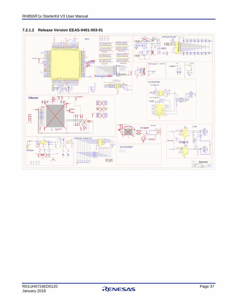
7.2 Schematics ................................................................................................................................ 36 7.2.1 Y-ASK-RH850F1L-V3 and Y-ASK-RH850F1K-V3 Schematics ......................................... 36 7.2.2 Y-ASK-RH850F1H-V3 Schematics ........................................................................................ 38 7.2.3 Y-ASK-RH850F1KM-S4-V3 Schematics ............................................................................... 39 7.2.4 Y-ASK-RH850F1KH-D8-V3 Schematics ............................................................................... 40
8. Revision History ................................................................................................................... 41

RH850/F1x StarterKit V3 User Manual
R01UH0724ED0120 Page 4 January 2018
1. Introduction The ‘RH850/F1x StarterKit’ serves as a simple and easy to use platform for evaluating the features and performance of Renesas Electronics’ 32-bit RH850/F1x microcontrollers.
Features:
• Connections for on-chip debugging and flash memory programming • Access to all microcontroller I/O pins • User interaction through potentiometer, rotary switch, buttons and LEDs • Serial interface connections for
− 1x RS232 − 1x LIN − 2x CAN-FD (RH850/F1L version does only support High Speed CAN) − 1x FlexRay (RH850/F1H, F1KM-S4 and F1KH-D8 version only) − 1x Ethernet 100Base-T (RH850/F1H, F1KM-S4 and F1KH-D8 version only)
• Power supply by RENESAS E1 On-Chip debugger or externally (12V DC input) • Support of different RH850/F1x family members
− RH850/F1L − RH850/F1K − RH850/F1H − RH850/F1KM-S4 − RH850/F1KH-D8
This document will describe the functionality provided by the StarterKit and guide the user through its operation. For details regarding the operation of the microcontroller refer to the RH850/F1x User Manuals.
RH850/F1x StarterKit V3 User Manual
R01UH0724ED0120 Page 5 January 2018
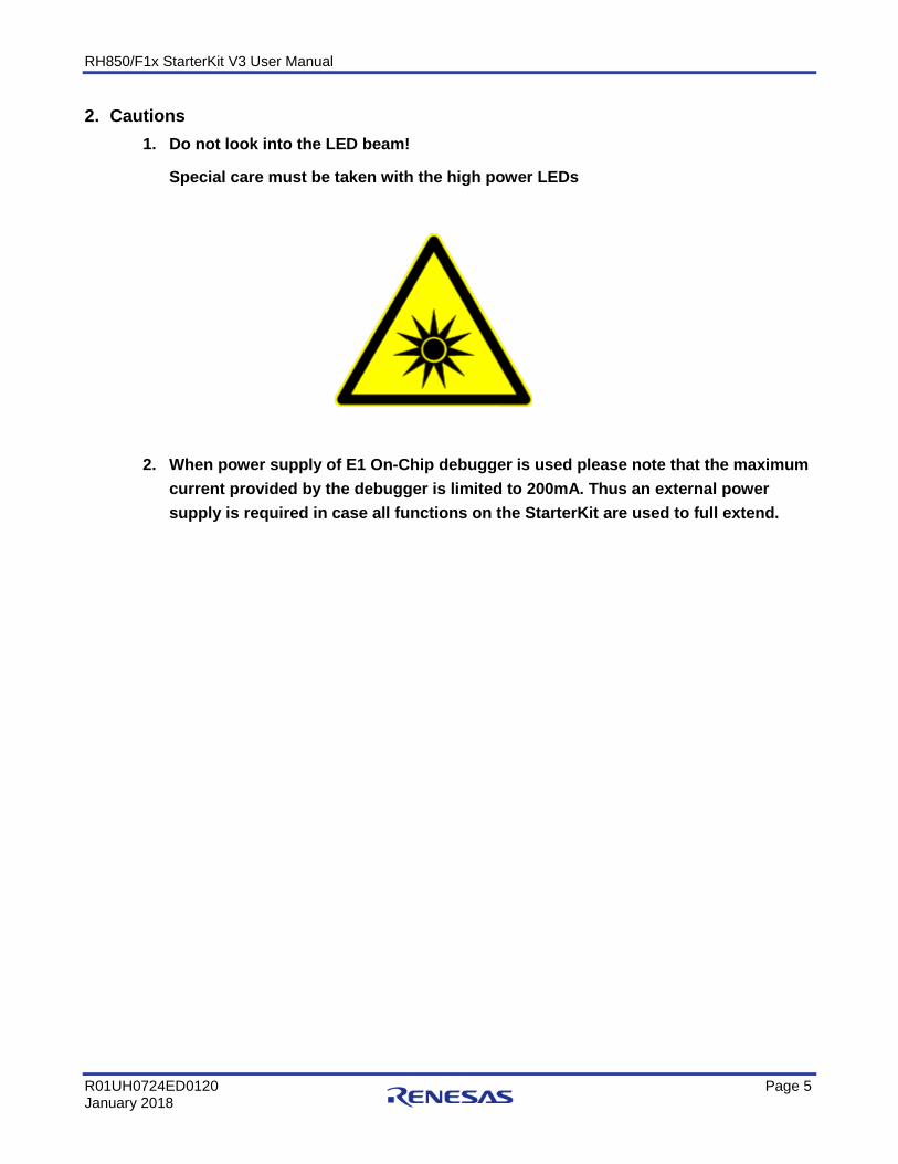
2. Cautions 1. Do not look into the LED beam!
Special care must be taken with the high power LEDs
2. When power supply of E1 On-Chip debugger is used please note that the maximum current provided by the debugger is limited to 200mA. Thus an external power supply is required in case all functions on the StarterKit are used to full extend.
RH850/F1x StarterKit V3 User Manual
R01UH0724ED0120 Page 6 January 2018
3. Quick Start Information
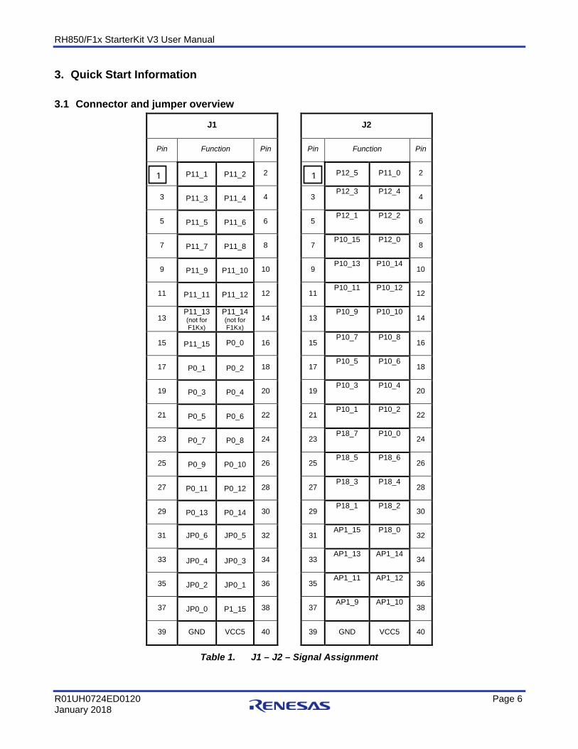
3.1 Connector and jumper overview
J1 J2
Pin Function Pin Pin Function Pin
P11_1 P11_2 2 P12_5 P11_0 2
3 P11_3 P11_4 4 3 P12_3 P12_4
4
5 P11_5 P11_6 6 5 P12_1 P12_2
6
7 P11_7 P11_8 8 7 P10_15 P12_0
8
9 P11_9 P11_10 10 9 P10_13 P10_14
10
11 P11_11 P11_12 12 11 P10_11 P10_12
12
13 P11_13 (not for F1Kx)
P11_14 (not for F1Kx)
14 13 P10_9 P10_10
14
15 P11_15 P0_0 16 15 P10_7 P10_8
16
17 P0_1 P0_2 18 17 P10_5 P10_6
18
19 P0_3 P0_4 20 19 P10_3 P10_4
20
21 P0_5 P0_6 22 21 P10_1 P10_2
22
23 P0_7 P0_8 24 23 P18_7 P10_0
24
25 P0_9 P0_10 26 25 P18_5 P18_6
26
27 P0_11 P0_12 28 27 P18_3 P18_4
28
29 P0_13 P0_14 30 29 P18_1 P18_2
30
31 JP0_6 JP0_5 32 31 AP1_15 P18_0
32
33 JP0_4 JP0_3 34 33 AP1_13 AP1_14
34
35 JP0_2 JP0_1 36 35 AP1_11 AP1_12
36
37 JP0_0 P1_15 38 37 AP1_9 AP1_10
38
39 GND VCC5 40 39 GND VCC5 40
Table 1. J1 – J2 – Signal Assignment
1 1
RH850/F1x StarterKit V3 User Manual
R01UH0724ED0120 Page 7 January 2018
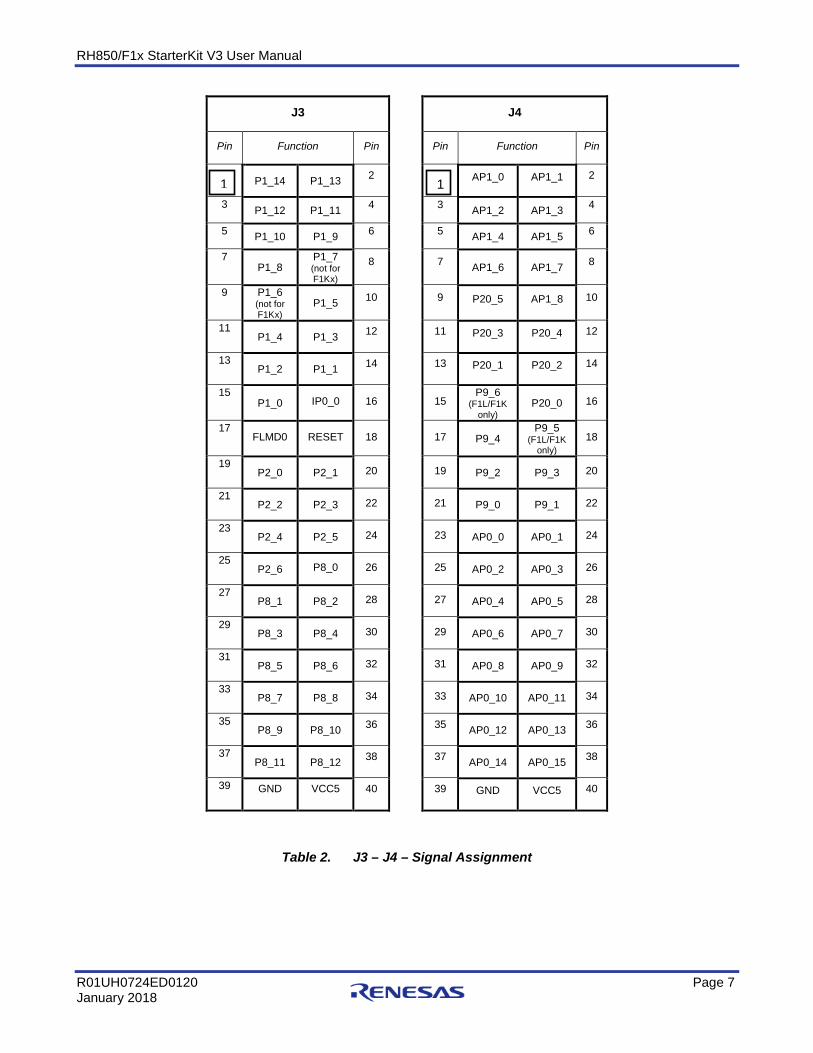
J3 J4
Pin Function Pin Pin Function Pin
P1_14 P1_13 2 AP1_0 AP1_1 2
3 P1_12 P1_11 4 3 AP1_2 AP1_3 4
5 P1_10 P1_9 6 5 AP1_4 AP1_5 6
7 P1_8
P1_7 (not for F1Kx)
8 7 AP1_6 AP1_7 8
9 P1_6 (not for F1Kx)
P1_5 10 9 P20_5 AP1_8 10
11 P1_4 P1_3 12 11 P20_3 P20_4 12
13 P1_2 P1_1 14 13 P20_1 P20_2 14
15 P1_0 IP0_0 16 15
P9_6 (F1L/F1K
only) P20_0 16
17 FLMD0 RESET 18 17 P9_4
P9_5 (F1L/F1K
only) 18
19 P2_0 P2_1 20 19 P9_2 P9_3 20
21 P2_2 P2_3 22 21 P9_0 P9_1 22
23 P2_4 P2_5 24 23 AP0_0 AP0_1 24
25 P2_6 P8_0 26 25 AP0_2 AP0_3 26
27 P8_1 P8_2 28 27 AP0_4 AP0_5 28
29 P8_3 P8_4 30 29 AP0_6 AP0_7 30
31 P8_5 P8_6 32 31 AP0_8 AP0_9 32
33 P8_7 P8_8 34 33 AP0_10 AP0_11 34
35 P8_9 P8_10 36 35 AP0_12 AP0_13 36
37 P8_11 P8_12 38 37 AP0_14 AP0_15 38
39 GND VCC5 40 39 GND VCC5 40
Table 2. J3 – J4 – Signal Assignment
1 1
RH850/F1x StarterKit V3 User Manual
R01UH0724ED0120 Page 8 January 2018
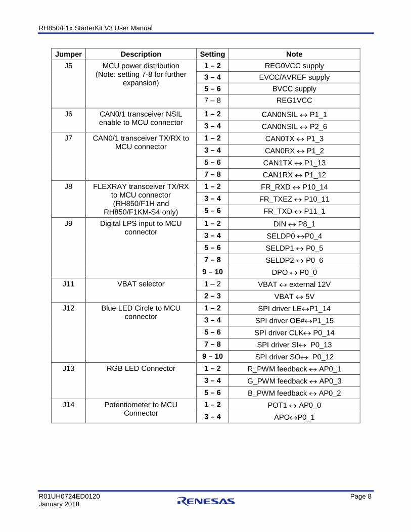
Jumper Description Setting Note J5
MCU power distribution (Note: setting 7-8 for further
expansion)
1 – 2 REG0VCC supply 3 – 4 EVCC/AVREF supply 5 – 6 BVCC supply 7 – 8 REG1VCC
J6 CAN0/1 transceiver NSIL enable to MCU connector
1 – 2 CAN0NSIL ↔ P1_1 3 – 4 CAN0NSIL ↔ P2_6
J7 CAN0/1 transceiver TX/RX to MCU connector
1 – 2 CAN0TX ↔ P1_3 3 – 4 CAN0RX ↔ P1_2 5 – 6 CAN1TX ↔ P1_13 7 – 8 CAN1RX ↔ P1_12
J8 FLEXRAY transceiver TX/RX to MCU connector (RH850/F1H and
RH850/F1KM-S4 only)
1 – 2 FR_RXD ↔ P10_14 3 – 4 FR_TXEZ ↔ P10_11 5 – 6 FR_TXD ↔ P11_1
J9 Digital LPS input to MCU connector
1 – 2 DIN ↔ P8_1 3 – 4 SELDP0 ↔P0_4 5 – 6 SELDP1 ↔ P0_5 7 – 8 SELDP2 ↔ P0_6 9 – 10 DPO ↔ P0_0
J11 VBAT selector 1 – 2 VBAT ↔ external 12V 2 – 3 VBAT ↔ 5V
J12 Blue LED Circle to MCU connector
1 – 2 SPI driver LE↔P1_14 3 – 4 SPI driver OE#↔P1_15 5 – 6 SPI driver CLK↔ P0_14 7 – 8 SPI driver SI↔ P0_13 9 – 10 SPI driver SO↔ P0_12
J13 RGB LED Connector 1 – 2 R_PWM feedback ↔ AP0_1 3 – 4 G_PWM feedback ↔ AP0_3 5 – 6 B_PWM feedback ↔ AP0_2
J14 Potentiometer to MCU Connector
1 – 2 POT1 ↔ AP0_0 3 – 4 APO↔P0_1
RH850/F1x StarterKit V3 User Manual
R01UH0724ED0120 Page 9 January 2018
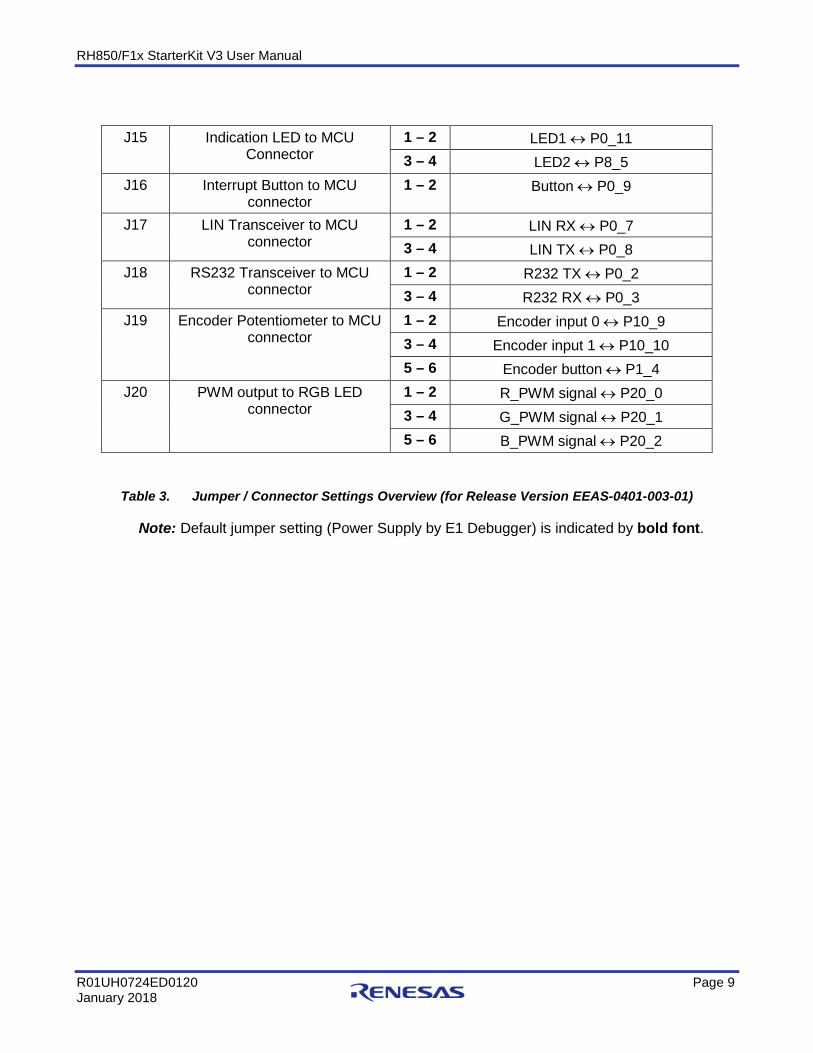
Table 3. Jumper / Connector Settings Overview (for Release Version EEAS-0401-003-01)
Note: Default jumper setting (Power Supply by E1 Debugger) is indicated by bold font.
J15 Indication LED to MCU Connector
1 – 2 LED1 ↔ P0_11 3 – 4 LED2 ↔ P8_5
J16 Interrupt Button to MCU connector
1 – 2 Button ↔ P0_9
J17 LIN Transceiver to MCU connector
1 – 2 LIN RX ↔ P0_7 3 – 4 LIN TX ↔ P0_8
J18 RS232 Transceiver to MCU connector
1 – 2 R232 TX ↔ P0_2 3 – 4 R232 RX ↔ P0_3
J19
Encoder Potentiometer to MCU connector
1 – 2 Encoder input 0 ↔ P10_9 3 – 4 Encoder input 1 ↔ P10_10 5 – 6 Encoder button ↔ P1_4
J20
PWM output to RGB LED connector
1 – 2 R_PWM signal ↔ P20_0 3 – 4 G_PWM signal ↔ P20_1 5 – 6 B_PWM signal ↔ P20_2
RH850/F1x StarterKit V3 User Manual
R01UH0724ED0120 Page 10 January 2018
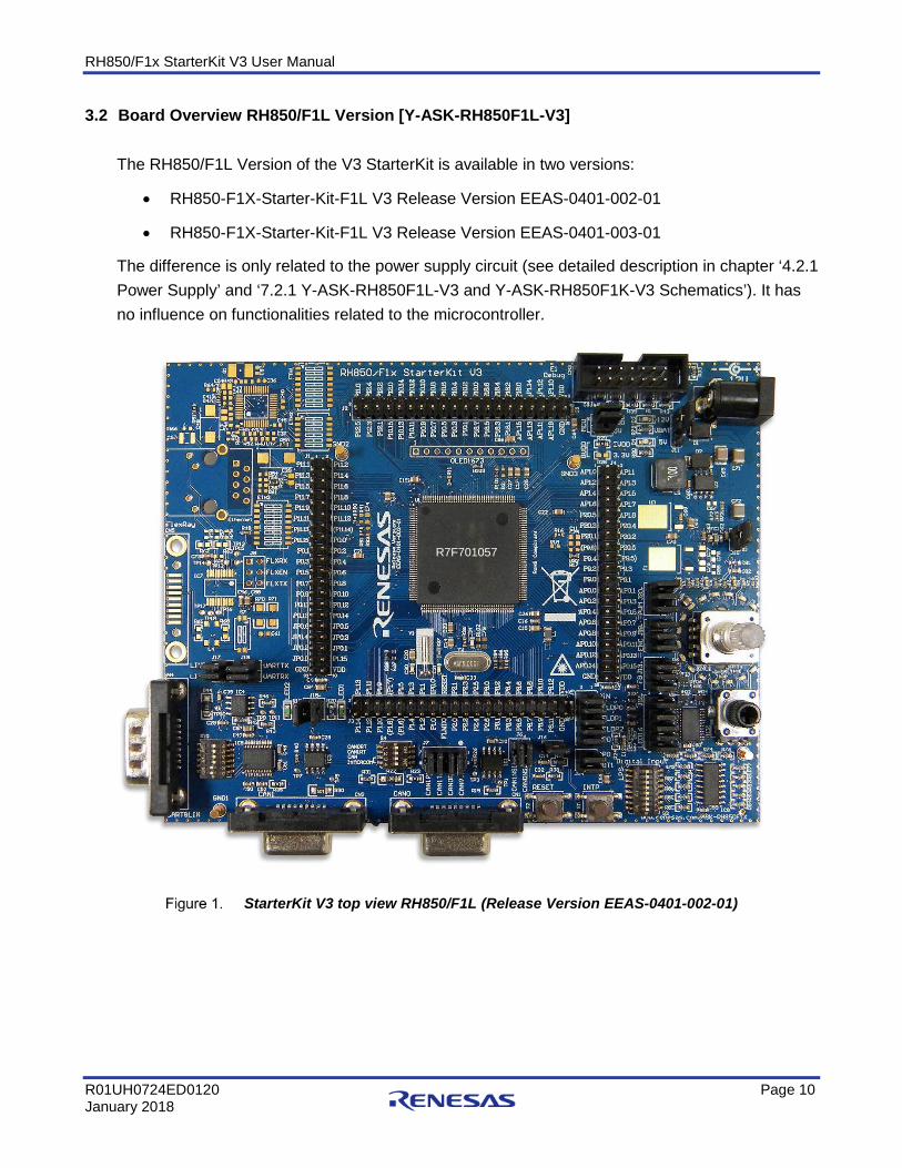
3.2 Board Overview RH850/F1L Version [Y-ASK-RH850F1L-V3]
The RH850/F1L Version of the V3 StarterKit is available in two versions:
• RH850-F1X-Starter-Kit-F1L V3 Release Version EEAS-0401-002-01
• RH850-F1X-Starter-Kit-F1L V3 Release Version EEAS-0401-003-01
The difference is only related to the power supply circuit (see detailed description in chapter ‘4.2.1 Power Supply’ and ‘7.2.1 Y-ASK-RH850F1L-V3 and Y-ASK-RH850F1K-V3 Schematics’). It has no influence on functionalities related to the microcontroller.
StarterKit V3 top view RH850/F1L (Release Version EEAS-0401-002-01)
R7F701057
RH850/F1x StarterKit V3 User Manual
R01UH0724ED0120 Page 11 January 2018
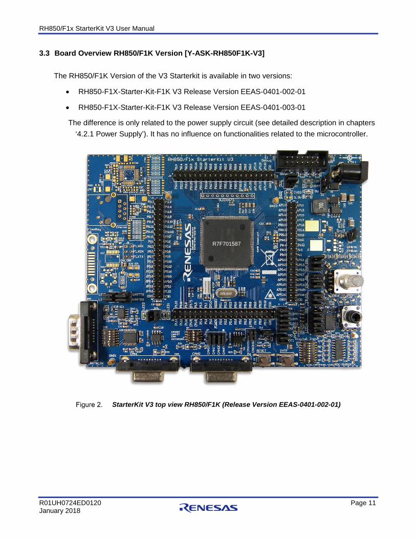
3.3 Board Overview RH850/F1K Version [Y-ASK-RH850F1K-V3]
The RH850/F1K Version of the V3 Starterkit is available in two versions:
• RH850-F1X-Starter-Kit-F1K V3 Release Version EEAS-0401-002-01
• RH850-F1X-Starter-Kit-F1K V3 Release Version EEAS-0401-003-01
The difference is only related to the power supply circuit (see detailed description in chapters ‘4.2.1 Power Supply’). It has no influence on functionalities related to the microcontroller.
StarterKit V3 top view RH850/F1K (Release Version EEAS-0401-002-01)
R7F701587
RH850/F1x StarterKit V3 User Manual
R01UH0724ED0120 Page 12 January 2018
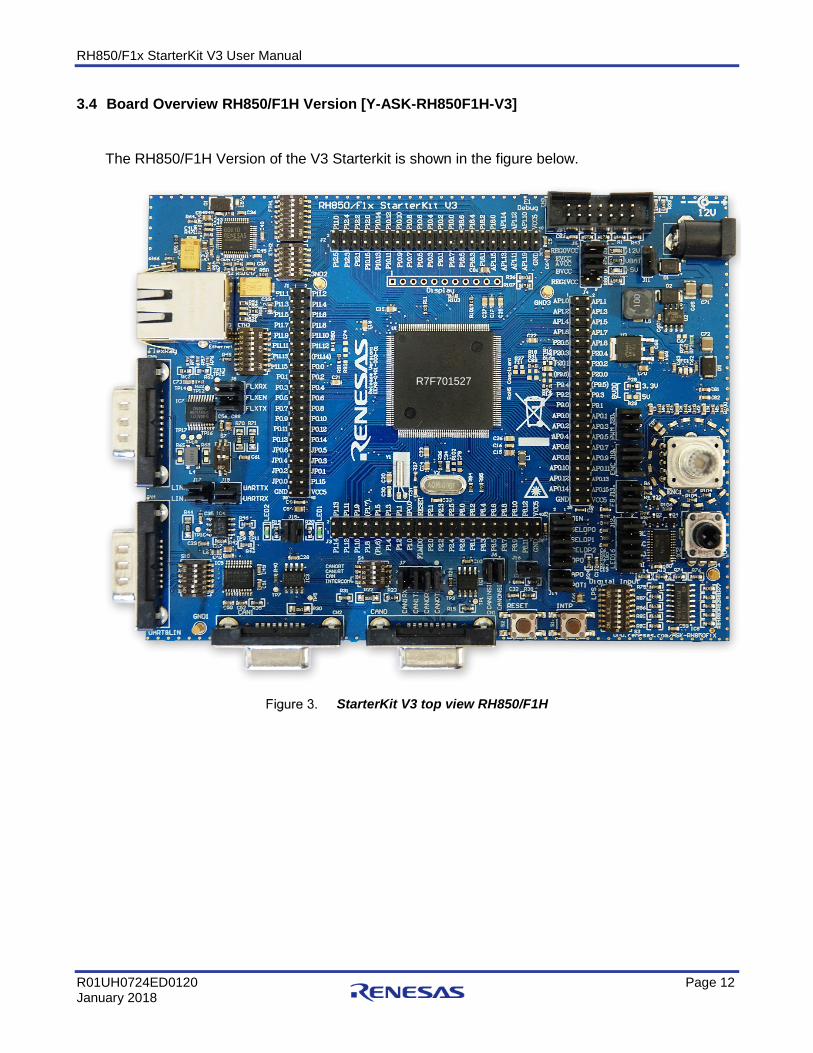
3.4 Board Overview RH850/F1H Version [Y-ASK-RH850F1H-V3]
The RH850/F1H Version of the V3 Starterkit is shown in the figure below.
StarterKit V3 top view RH850/F1H
R7F701527

RH850/F1x StarterKit V3 User Manual
R01UH0724ED0120 Page 13 January 2018
3.5 Board Overview RH850/F1KM-S4 Version [Y-ASK-RH850F1KM-S4-V3]
The RH850/F1KM-S4 Version of the V3 StarterKit is shown in the figure below.
StarterKit V3 top view RH850/F1KM-S4
R7F701649
RH850/F1x StarterKit V3 User Manual
R01UH0724ED0120 Page 14 January 2018
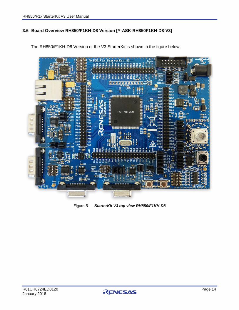
3.6 Board Overview RH850/F1KH-D8 Version [Y-ASK-RH850F1KH-D8-V3]
The RH850/F1KH-D8 Version of the V3 StarterKit is shown in the figure below.
StarterKit V3 top view RH850/F1KH-D8
R7F701709
RH850/F1x StarterKit V3 User Manual
R01UH0724ED0120 Page 15 January 2018
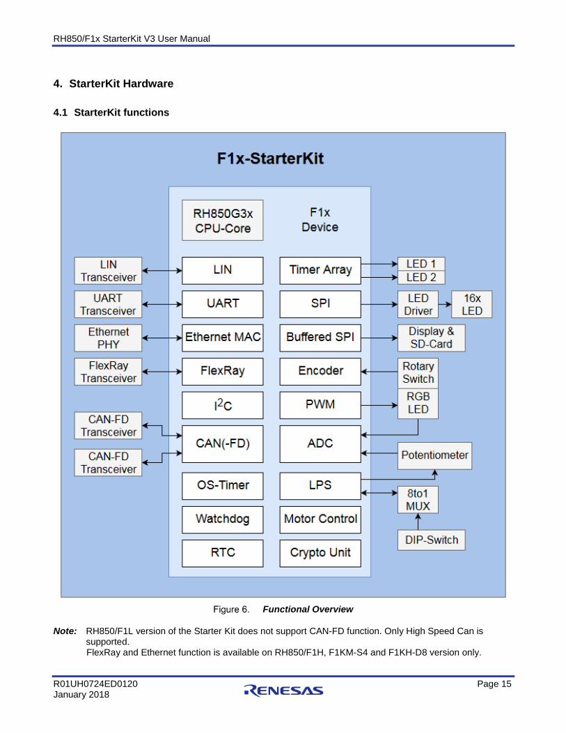
4. StarterKit Hardware
4.1 StarterKit functions
Functional Overview
Note: RH850/F1L version of the Starter Kit does not support CAN-FD function. Only High Speed Can is supported.
FlexRay and Ethernet function is available on RH850/F1H, F1KM-S4 and F1KH-D8 version only.
RH850/F1x StarterKit V3 User Manual
R01UH0724ED0120 Page 16 January 2018
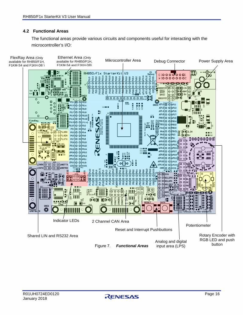
4.2 Functional Areas The functional areas provide various circuits and components useful for interacting with the microcontroller’s I/O:
Functional Areas
Shared LIN and RS232 Area Reset and Interrupt Pushbuttons
Potentiometer
Debug Connector Mikrocontroller Area Power Supply Area
Indicator LEDs
FlexRay Area (Only available for RH850/F1H, F1KM-S4 and F1KH-D8 )
2 Channel CAN Area
Analog and digital input area (LPS)
Rotary Encoder with RGB LED and push
button
Ethernet Area (Only available for RH850/F1H, F1KM-S4 and F1KH-D8)
RH850/F1x StarterKit V3 User Manual
R01UH0724ED0120 Page 17 January 2018
4.2.1 Power Supply
4.2.1.1 Power supply configuration
The StarterKit provides two options for powering the board’s integrated circuits. It is possible to supply the StarterKit by using the E1 Debugger or it is possible to supply the StarterKit by using an external 12 Volt power supply.
With the default jumper setting (see 0) the StarterKit is configured to be power supplied by the E1 Debugger.
The operation of the LIN and the FlexRay interface is only possible by using an external 12 Volt power supply.
When the board is supplied externally by 12 Volt, please choose the following jumper settings:
Jumper Description Setting Note J11 VBAT selector 1-2 closed (12V)
2-3 Open J10 Voltage regulator output to VDD Connector
(only available on StarterKit Release Version EEAS-0401-002-01) 1-2 closed
Table 4. Jumper setting for external 12 volt power supply
When the board is supplied by E1 debugger, please choose the following jumper settings:
Jumper Description Setting Note J11 VBAT selector 1-2 open
2-3 closed (5V) J10 Voltage regulator output to VDD Connector
(only available on StarterKit Release Version EEAS-0401-002-01) 1-2 open
Table 5. Jumper setting for power supply by E1 Debugger
The power supply area includes a DC jack type connector for providing external power supply to the StarterKit and its components. The external supply is reversibly protected against overvoltage. Nevertheless, please always observe the right polarity and voltage.
Connector Description Input Voltage
Range PowerCon DC Power Jack ID=2.0mm, center positive +10V to +15V
Table 6. Power supply connector specification
The two indicator LEDs (D3 and D4) are showing which power supply voltages are available.
RH850/F1x StarterKit V3 User Manual
R01UH0724ED0120 Page 18 January 2018
4.2.1.2 Power supply measurement
The current which is consumed by MCU can be measured by using J5. The appearance of J5 is different on the two Release Version. Please find below a description of the different versions.
RH850/F1L and RH850/F1K:
Jumper Description Pins Note J5 MCU power
measurement 1-2 REGVCC power supply (5 V) 3-4 EVCC, AV0REF, A1VREF power supply (5 V) 5-6 BVCC (5 V) 7-8 (not used)
Table 7. RH850/F1L and RH850/F1K MCU power measurement on Release Version EEAS-0401-003-01
Jumper Description Pins Note for RH850/F1L and RH850/F1K J5 MCU power
measurement 1-2 REGVCC power supply (5 V) 3-4 Total MCU power supply (5 V)
Table 8. RH850/F1L and RH850/F1K MCU power measurement on Release Version EEAS-0401-002-01
RH850/F1H and RH850/F1KM-S4:
Jumper Description Pins Note J5 MCU power
measurement 1-2 REGVCC power supply (5 V) 3-4 EVCC, AV0REF, A1VREF power supply (5 V) 5-6 BVCC (3,3 V) 7-8 (not used)
Table 9. RH850/F1H MCU power measurement on Release Version EEAS-0401-003-01
RH850/F1x StarterKit V3 User Manual
R01UH0724ED0120 Page 19 January 2018
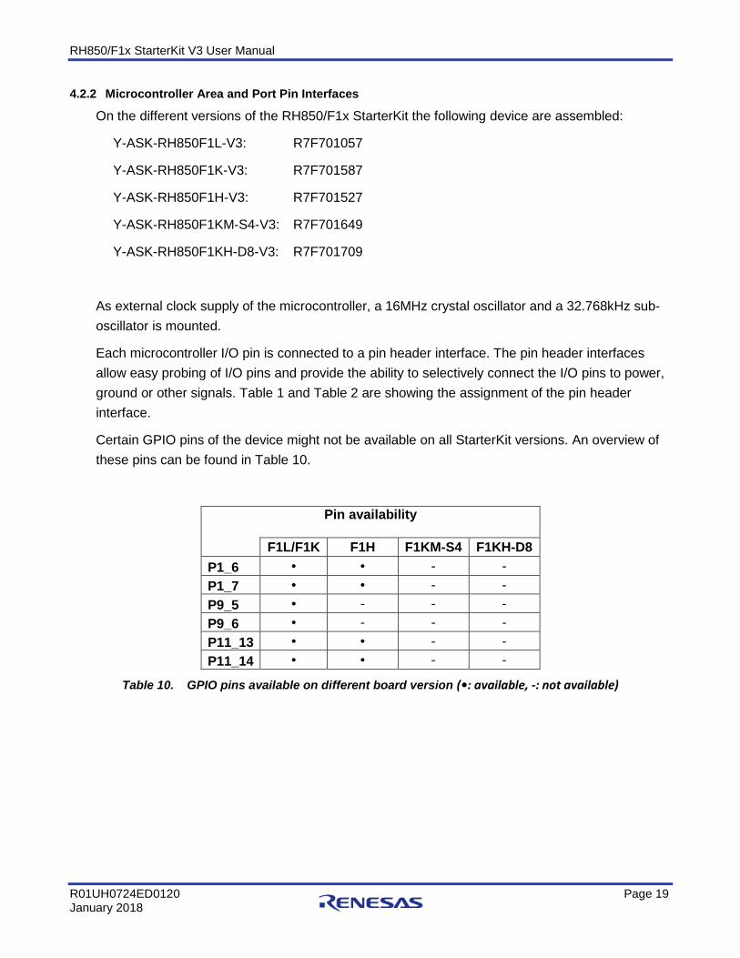
4.2.2 Microcontroller Area and Port Pin Interfaces
On the different versions of the RH850/F1x StarterKit the following device are assembled:
Y-ASK-RH850F1L-V3: R7F701057
Y-ASK-RH850F1K-V3: R7F701587
Y-ASK-RH850F1H-V3: R7F701527
Y-ASK-RH850F1KM-S4-V3: R7F701649
Y-ASK-RH850F1KH-D8-V3: R7F701709
As external clock supply of the microcontroller, a 16MHz crystal oscillator and a 32.768kHz sub-oscillator is mounted.
Each microcontroller I/O pin is connected to a pin header interface. The pin header interfaces allow easy probing of I/O pins and provide the ability to selectively connect the I/O pins to power, ground or other signals. Table 1 and Table 2 are showing the assignment of the pin header interface.
Certain GPIO pins of the device might not be available on all StarterKit versions. An overview of these pins can be found in Table 10.
Pin availability
F1L/F1K F1H F1KM-S4 F1KH-D8 P1_6 • • - - P1_7 • • - - P9_5 • - - - P9_6 • - - - P11_13 • • - - P11_14 • • - -
Table 10. GPIO pins available on different board version (•: available, -: not available)
RH850/F1x StarterKit V3 User Manual
R01UH0724ED0120 Page 20 January 2018
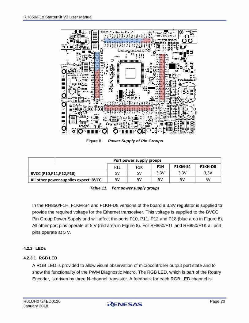
Power Supply of Pin Groups
Port power supply groups F1L F1K F1H F1KM-S4 F1KH-D8 BVCC (P10,P11,P12,P18) 5V 5V 3,3V 3,3V 3,3V All other power supplies expect BVCC 5V 5V 5V 5V 5V
Table 11. Port power supply groups
In the RH850/F1H, F1KM-S4 and F1KH-D8 versions of the board a 3.3V regulator is supplied to provide the required voltage for the Ethernet transceiver. This voltage is supplied to the BVCC Pin Group Power Supply and will affect the ports P10, P11, P12 and P18 (blue area in Figure 8). All other port pins operate at 5 V (red area in Figure 8). For RH850/F1L and RH850/F1K all port pins operate at 5 V.
4.2.3 LEDs
4.2.3.1 RGB LED
A RGB LED is provided to allow visual observation of microcontroller output port state and to show the functionality of the PWM Diagnostic Macro. The RGB LED, which is part of the Rotary Encoder, is driven by three N-channel transistor. A feedback for each RGB LED channel is
RH850/F1x StarterKit V3 User Manual
R01UH0724ED0120 Page 21 January 2018
connected to the A/D converter of the microcontroller to evaluate the LED drive state. The LED PWM signals are active high.
Please use the following jumper configuration to activate the full RGB LED functionality:
Jumper Description Setting Note J20 RGB LED PWM
connector 1-2 Red PWM channel↔ P20_1 3-4 Green PWM channel ↔ P20_2 5-6 Blue PWM channel ↔ P20_3
J13 RGB LED feedback connector
1-2 Red LED feedback channel ↔ AP0_1 3-4 Green LED feedback channel ↔ AP0_2 5-6 Blue LED feedback channel ↔ AP0_3
Table 12. White RGB Signals Configuration
4.2.3.2 Green Indicator LEDs
Two green low power LEDs (LED1 and LED2) are provided to allow visual observation of microcontroller output port states. The LED signals are active high.
Jumper Setting LED Device Port J15 1-2 LED1 P0_11
3-4 LED2 P8_5
Table 13. Green Indicator LED Signals
4.2.3.3 Blue Power Supply LEDs
Two blue LEDs (D5 and D6) are provided to allow visual observation of the power supply status.
LED Note D3 12 Volt power supply D4 5 Volt power supply
Table 14. Blue Power Supply LED Signals
4.2.3.4 Blue LED Circle
Sixteen blue LEDs are driven by the TLC5925, which can controlled by the SPI command to change the output states.
RH850/F1x StarterKit V3 User Manual
R01UH0724ED0120 Page 22 January 2018
Jumper Setting Signal Device Port J12 1-2 LAT P1_14
3-4 BLNK P1_15 5-6 MCLK P0_14 7-8 MOSI P0_13
9-10 MISO P0_12
Table 15. Blue LED Circle Signals
4.2.4 Digital inputs for Low Power Sampler (LPS)
Eight digital input signals, which are generated by a DIP switch array (S3), are provided to trigger the microcontroller’s Low Power Sampler. The input signals are connected to the microcontroller via 8 to 1 Multiplexer (IC4). When the DIP switches (S3) are changed during low power mode (DeepSTOP mode), the microcontroller will wake up.
Please use the following jumper configuration to connect the DIP Switch and multiplexer to the microcontroller
Jumper Description Setting Note J9 Digital LPS input
to MCU connector
1 – 2 DIN ↔ P8_1 3 – 4 SELDP0 ↔P0_4 5 – 6 SELDP1 ↔ P0_5 7 – 8 SELDP2 ↔ P0_6 9 – 10 DPO ↔ P0_0
Table 16. LPS Jumper Configuration
4.2.5 Pushbutton Switches
Two pushbutton switches (S1and S2) are provided to allow the switching of microcontroller input port states. The switches are active low and normally open.
Switch Device signal Active Level Inactive State S1 P0_9 (INTP12) low open S2 RESET low open
Table 17. Pushbutton Switch Signals
Please use the following jumper configuration to connect the interrupt pushbutton switch (S1) to the microcontroller.
Jumper Description Setting Note J16 Interrupt Button to MCU connector 1-2 Button ↔ P0_9
Table 18. Interrupt Pushbutton Jumper Configuration
RH850/F1x StarterKit V3 User Manual
R01UH0724ED0120 Page 23 January 2018
Additionally a pushbutton is provided with the Rotary Encoder. For details please refer to Rotary Encoder with Pushbutton.
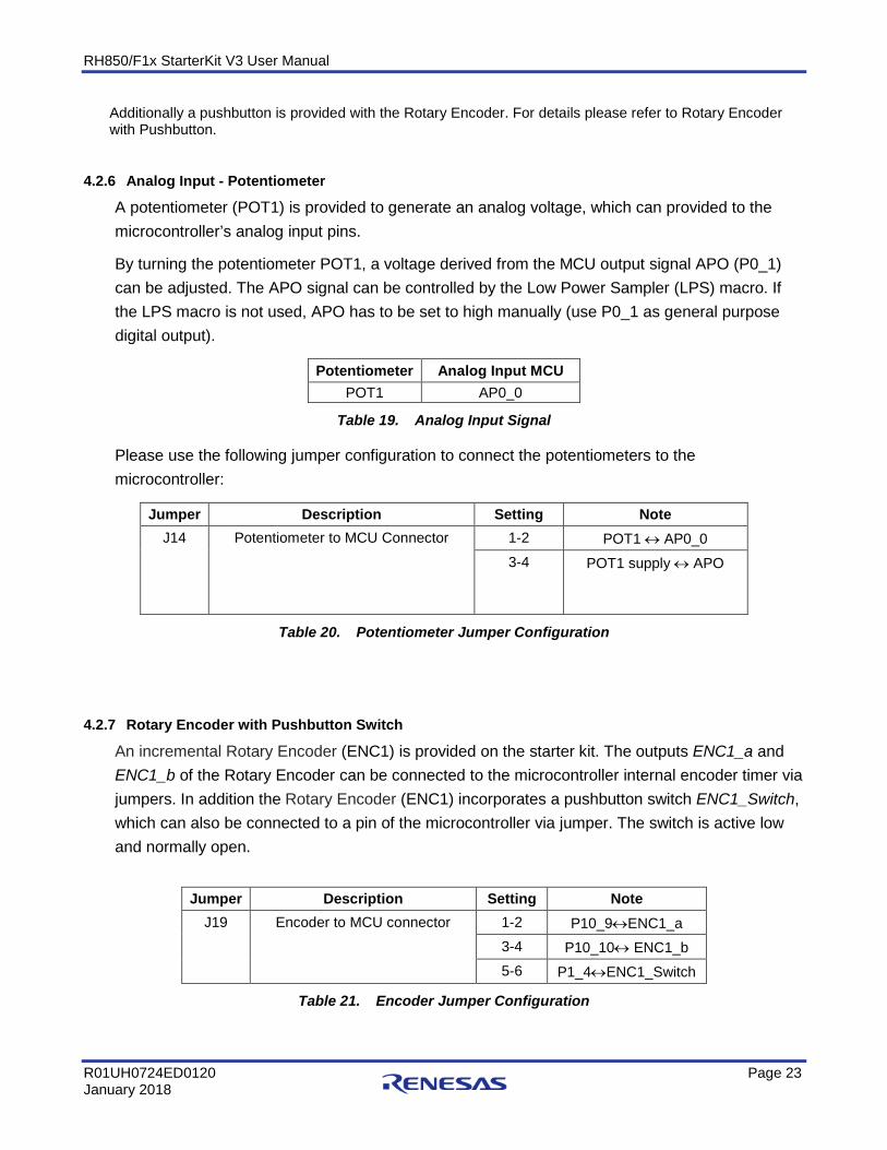
4.2.6 Analog Input - Potentiometer
A potentiometer (POT1) is provided to generate an analog voltage, which can provided to the microcontroller’s analog input pins.
By turning the potentiometer POT1, a voltage derived from the MCU output signal APO (P0_1) can be adjusted. The APO signal can be controlled by the Low Power Sampler (LPS) macro. If the LPS macro is not used, APO has to be set to high manually (use P0_1 as general purpose digital output).
Potentiometer Analog Input MCU POT1 AP0_0
Table 19. Analog Input Signal
Please use the following jumper configuration to connect the potentiometers to the microcontroller:
Jumper Description Setting Note J14 Potentiometer to MCU Connector 1-2 POT1 ↔ AP0_0
3-4 POT1 supply ↔ APO
Table 20. Potentiometer Jumper Configuration
4.2.7 Rotary Encoder with Pushbutton Switch
An incremental Rotary Encoder (ENC1) is provided on the starter kit. The outputs ENC1_a and ENC1_b of the Rotary Encoder can be connected to the microcontroller internal encoder timer via jumpers. In addition the Rotary Encoder (ENC1) incorporates a pushbutton switch ENC1_Switch, which can also be connected to a pin of the microcontroller via jumper. The switch is active low and normally open.
Jumper Description Setting Note
J19 Encoder to MCU connector 1-2 P10_9↔ENC1_a 3-4 P10_10↔ ENC1_b 5-6 P1_4↔ENC1_Switch
Table 21. Encoder Jumper Configuration
RH850/F1x StarterKit V3 User Manual
R01UH0724ED0120 Page 24 January 2018
4.2.8 Serial Communication Interfaces
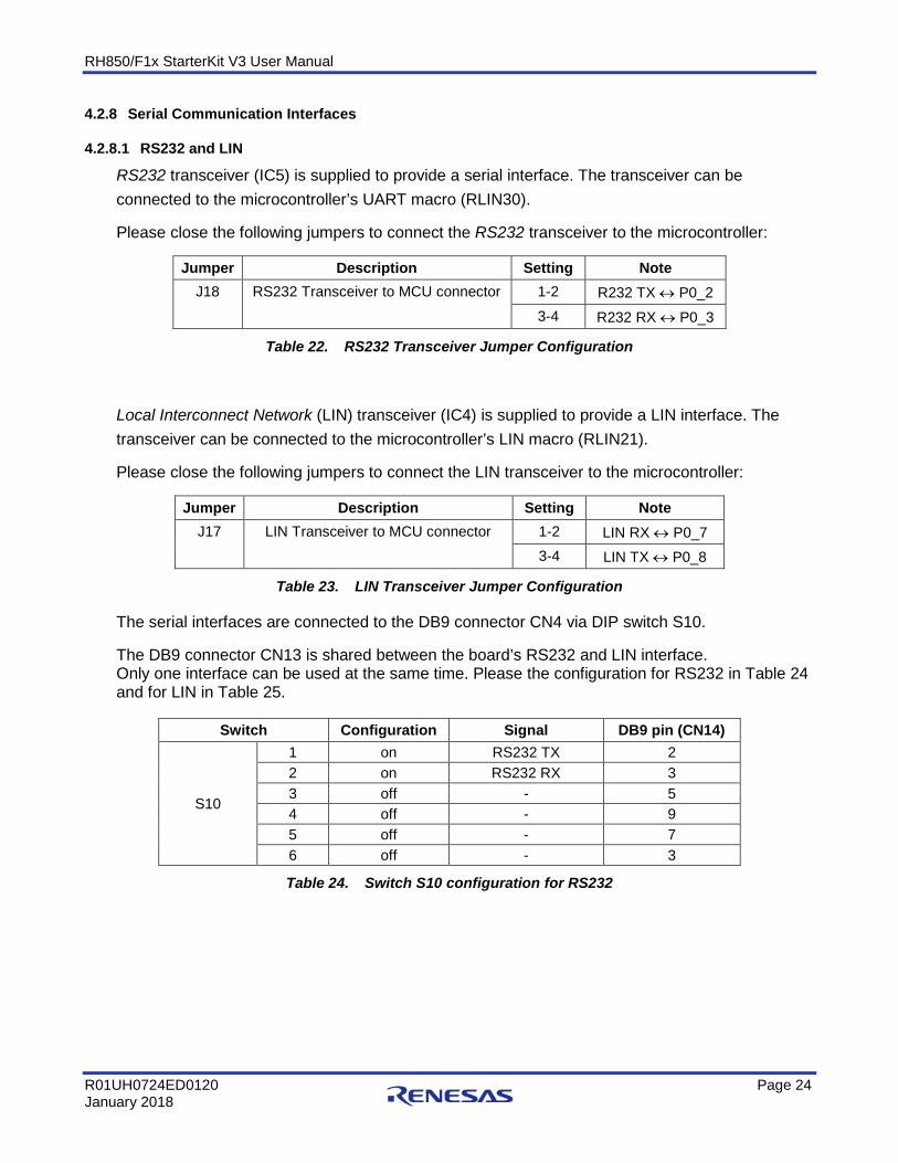
4.2.8.1 RS232 and LIN
RS232 transceiver (IC5) is supplied to provide a serial interface. The transceiver can be connected to the microcontroller’s UART macro (RLIN30).
Please close the following jumpers to connect the RS232 transceiver to the microcontroller:
Jumper Description Setting Note J18 RS232 Transceiver to MCU connector 1-2 R232 TX ↔ P0_2
3-4 R232 RX ↔ P0_3
Table 22. RS232 Transceiver Jumper Configuration
Local Interconnect Network (LIN) transceiver (IC4) is supplied to provide a LIN interface. The transceiver can be connected to the microcontroller’s LIN macro (RLIN21).
Please close the following jumpers to connect the LIN transceiver to the microcontroller:
Jumper Description Setting Note J17 LIN Transceiver to MCU connector 1-2 LIN RX ↔ P0_7
3-4 LIN TX ↔ P0_8
Table 23. LIN Transceiver Jumper Configuration
The serial interfaces are connected to the DB9 connector CN4 via DIP switch S10.
The DB9 connector CN13 is shared between the board’s RS232 and LIN interface. Only one interface can be used at the same time. Please the configuration for RS232 in Table 24 and for LIN in Table 25.
Switch Configuration Signal DB9 pin (CN14)
S10
1 on RS232 TX 2 2 on RS232 RX 3 3 off - 5 4 off - 9 5 off - 7 6 off - 3
Table 24. Switch S10 configuration for RS232
RH850/F1x StarterKit V3 User Manual
R01UH0724ED0120 Page 25 January 2018
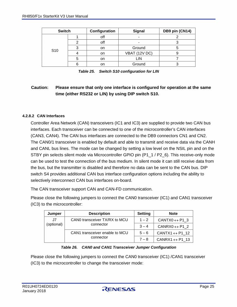
Switch Configuration Signal DB9 pin (CN14)
S10
1 off - 2 2 off - 3 3 on Ground 5 4 on VBAT (12V DC) 9 5 on LIN 7 6 on Ground 3
Table 25. Switch S10 configuration for LIN
Caution: Please ensure that only one interface is configured for operation at the same time (either RS232 or LIN) by using DIP switch S10.
4.2.8.2 CAN Interfaces
Controller Area Network (CAN) transceivers (IC1 and IC3) are supplied to provide two CAN bus interfaces. Each transceiver can be connected to one of the microcontroller’s CAN interfaces (CAN3, CAN4). The CAN bus interfaces are connected to the DB9 connectors CN1 and CN2. The CAN0/1 transceiver is enabled by default and able to transmit and receive data via the CANH and CANL bus lines. The mode can be changed by setting a low level on the NSIL pin and on the STBY pin selects silent mode via Microcontroller GPIO pin (P1_1 / P2_6). This receive-only mode can be used to test the connection of the bus medium. In silent mode it can still receive data from the bus, but the transmitter is disabled and therefore no data can be sent to the CAN bus. DIP switch S4 provides additional CAN bus interface configuration options including the ability to selectively interconnect CAN bus interfaces on-board.
The CAN transceiver support CAN and CAN-FD communication.
Please close the following jumpers to connect the CAN0 transceiver (IC1) and CAN1 transceiver (IC3) to the microcontroller:
Jumper Description Setting Note J7
(optional) CAN0 transceiver TX/RX to MCU
connector 1 – 2 CANTX0 ↔ P1_3 3 – 4 CANRX0 ↔ P1_2
CAN1 transceiver enable to MCU connector
5 – 6 CANTX1 ↔ P1_12 7 – 8 CANRX1 ↔ P1_13
Table 26. CAN0 and CAN1 Transceiver Jumper Configuration
Please close the following jumpers to connect the CAN0 transceiver (IC1) /CAN1 transceiver (IC3) to the microcontroller to change the transceiver mode:
RH850/F1x StarterKit V3 User Manual
R01UH0724ED0120 Page 26 January 2018
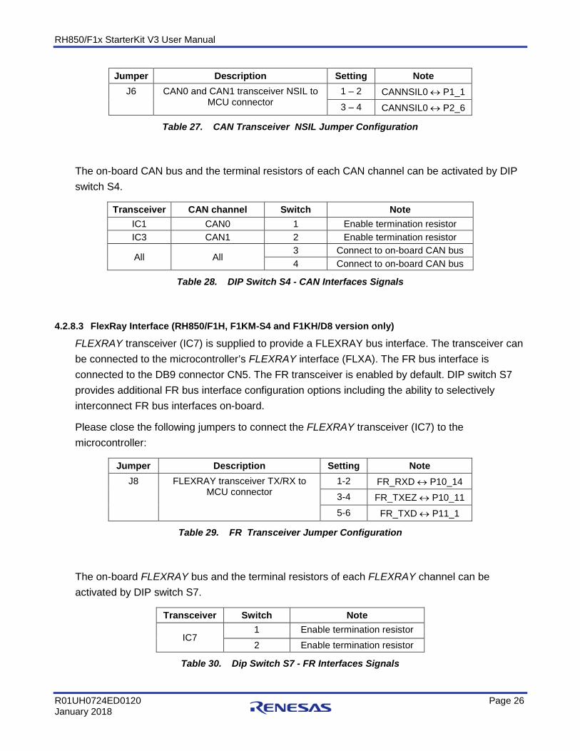
Jumper Description Setting Note J6 CAN0 and CAN1 transceiver NSIL to
MCU connector 1 – 2 CANNSIL0 ↔ P1_1 3 – 4 CANNSIL0 ↔ P2_6
Table 27. CAN Transceiver NSIL Jumper Configuration
The on-board CAN bus and the terminal resistors of each CAN channel can be activated by DIP switch S4.
Transceiver CAN channel Switch Note IC1 CAN0 1 Enable termination resistor IC3 CAN1 2 Enable termination resistor
All All 3 Connect to on-board CAN bus 4 Connect to on-board CAN bus
Table 28. DIP Switch S4 - CAN Interfaces Signals
4.2.8.3 FlexRay Interface (RH850/F1H, F1KM-S4 and F1KH/D8 version only)
FLEXRAY transceiver (IC7) is supplied to provide a FLEXRAY bus interface. The transceiver can be connected to the microcontroller’s FLEXRAY interface (FLXA). The FR bus interface is connected to the DB9 connector CN5. The FR transceiver is enabled by default. DIP switch S7 provides additional FR bus interface configuration options including the ability to selectively interconnect FR bus interfaces on-board.
Please close the following jumpers to connect the FLEXRAY transceiver (IC7) to the microcontroller:
Jumper Description Setting Note J8 FLEXRAY transceiver TX/RX to
MCU connector 1-2 FR_RXD ↔ P10_14 3-4 FR_TXEZ ↔ P10_11 5-6 FR_TXD ↔ P11_1
Table 29. FR Transceiver Jumper Configuration
The on-board FLEXRAY bus and the terminal resistors of each FLEXRAY channel can be activated by DIP switch S7.
Transceiver Switch Note
IC7 1 Enable termination resistor 2 Enable termination resistor
Table 30. Dip Switch S7 - FR Interfaces Signals
RH850/F1x StarterKit V3 User Manual
R01UH0724ED0120 Page 27 January 2018
4.2.8.4 Ethernet Interface RH850/F1H, F1KM-S4 and F1KH/D8 version only)
Ethernet PHY (IC6) is supplied to provide an external T100Base-TX Ethernet bus interface. The transceiver can be connected to the microcontroller’s Ethernet interface ETNB via the DIP switches ETH1 – ETH3.
Please use the following DIP switch configuration to connect the Ethernet transceiver to the microcontroller:
Switch Setting Note
ETH1
1 on ETH0LINK ↔ P18_0 2 on ETH0TXD0 ↔ P18_1 3 on ETH0TXD1 ↔ P18_2 4 on ETH0TXD2 ↔ P18_3 5 on ETH0TXD3 ↔ P18_4 6 on ETH0TXEN ↔ P18_5 7 on ETH0TXERR ↔ P18_6 8 on ETH0TXCLK ↔ P18_7
Table 31. DIP Switch ETH1
Switch Setting Note
ETH2
1 on ETH0RXCLK ↔ P10_0 2 on ETH0RXD0 ↔ P10_1 3 on ETH0RXD1 ↔ P10_2 4 on ETH0RXD2 ↔ P10_4 5 on ETH0RXD3 ↔ P10_5 6 X No function
Table 32. DIP Switch ETH2
Switch Setting Note
ETH2
1 on ETH0RESETB ↔ P11_9 2 on ETH0COLSD ↔ P11_10 3 on ETH0RXDV ↔ P11_11 4 on ETH0CRS ↔ P11_13 5 on ETH0RXERR ↔ P11_14 6 on ETH0MDIO ↔ P12_4 7 on ETH0MDC ↔ P12_5 8 on ETH0INT ↔ P11_6
Table 33. DIP Switch ETH3
RH850/F1x StarterKit V3 User Manual
R01UH0724ED0120 Page 28 January 2018
4.2.9 On-chip Debug and Flash Programming Connector
Connector CN3 is provided to allow the connection of microcontroller debug and flash programming tools. Connector CN3 is a 14 pin, 0.1” pin pitch connector. The pinout of this connector supports the Renesas E1 On-chip debug emulator. For more information about E1, please see Chapter 5.1 E1 On-Chip Debug Emulator [R0E000010KCE00].
4.2.10 OLED Board (optional)
The StarterKit offers a pin header to optionally connect an external display to the board. For example following OLED Display with microSD card holder is compatible to the connector: https://www.adafruit.com/products/1673
Header Pin number signal Note
Display
1 MOSI P11_2 2 SCK P11_3 3 DC(data command) P11_0 4 RESET P10_12 5 OLEDCS P11_15 6 SDCS P12_1 7 MISO P11_4 8 CD(card detected) P11_5 9 3Vo AP0_4
10 Vin VDD_5V 11 GND GND
Table 34. OLED header (optional)

RH850/F1x StarterKit V3 User Manual
R01UH0724ED0120 Page 29 January 2018
5. Development tools
5.1 E1 On-Chip Debug Emulator [R0E000010KCE00] The E1 On-Chip Debug Emulator is a powerful debugging tool with flash programming functions which supports various Renesas microcontrollers.
Updates and User Manuals for this tool can be found on the Renesas website:
http://www.renesas.com/e1
5.2 Development Software The following development software tools are included in the StarterKit package:
• Green Hills MULTI IDE (90 day evaluation version)
• IAR Embedded Workbench for Renesas RH850 (128KB Kickstart version)
• iSYSTEM winIDEA with E1 support
• CS+ integrated development environment (Evaluation Version via download)
• Renesas Flash Programmer (RFP)
• Code generator tool AP4 for RH850/F1K
More information about the usage of these software tools is shown in the Quick Start Guide which is also part of the StarterKit package.
RH850/F1x StarterKit V3 User Manual
R01UH0724ED0120 Page 30 January 2018
6. RH850/F1x StarterKit Example Software
The included demo software provides the following functions:
• Basic MCU Initialization
• PWM Generation for user LEDs and RGB LEDs
• PWM Diagnostic Function for RGB LEDs
• A/D-Converter for PWM-Diagnostics and Potentiometers
• Standby modes including Low Power Sampler (LPS)
• Push-Button Function
• Encoder Function
• CAN Frame Transmission
• LIN Frame Transmission
• UART Transmission
• SPI Transmission
• Operating System Timer
• Timer Array Unit J
• Timer Array Unit B
• Ethernet Demo with Webserver Application (RH850/F1H and RH850/F1KM-S4 only)
RH850/F1x StarterKit V3 User Manual
R01UH0724ED0120 Page 31 January 2018
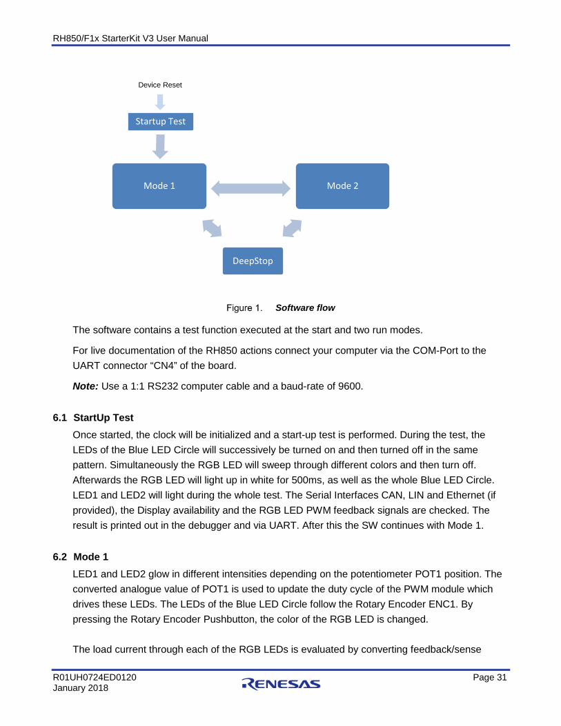
Software flow
The software contains a test function executed at the start and two run modes.
For live documentation of the RH850 actions connect your computer via the COM-Port to the UART connector “CN4” of the board.
Note: Use a 1:1 RS232 computer cable and a baud-rate of 9600.
6.1 StartUp Test Once started, the clock will be initialized and a start-up test is performed. During the test, the LEDs of the Blue LED Circle will successively be turned on and then turned off in the same pattern. Simultaneously the RGB LED will sweep through different colors and then turn off. Afterwards the RGB LED will light up in white for 500ms, as well as the whole Blue LED Circle. LED1 and LED2 will light during the whole test. The Serial Interfaces CAN, LIN and Ethernet (if provided), the Display availability and the RGB LED PWM feedback signals are checked. The result is printed out in the debugger and via UART. After this the SW continues with Mode 1.
6.2 Mode 1 LED1 and LED2 glow in different intensities depending on the potentiometer POT1 position. The converted analogue value of POT1 is used to update the duty cycle of the PWM module which drives these LEDs. The LEDs of the Blue LED Circle follow the Rotary Encoder ENC1. By pressing the Rotary Encoder Pushbutton, the color of the RGB LED is changed. The load current through each of the RGB LEDs is evaluated by converting feedback/sense
Startup Test
Mode 2
DeepStop
Mode 1
Device Reset
RH850/F1x StarterKit V3 User Manual
R01UH0724ED0120 Page 32 January 2018
signal into digital values and applying conversion result upper / lower limit check function of ADC (PWM diagnostic function). In case the measured current is either too high or too low, a fault is assumed and in turn the PWM of the corresponding LED is switched OFF. By switching to Mode 2 the PWM output and diagnostic is started again. If Ethernet is available (RH850/F1H and RH850/F1KM-S4 only) the corresponding Webserver Handler is called periodically.
A short push on pushbutton S1 will switch to mode 2, holding it pressed for 3s or more will switch to DeepSTOP mode.
After 30s without user action, the microcontroller will enter DeepSTOP mode on its own.
Mode 1 is called in a 1ms cycle using the Operating System Timer.
6.3 Mode 2 LED1 and LED2 blink alternately and the LEDs of the Blue LED Circle run around the Rotary Encoder in a specific frequency. The frequency is determined by the analogue value of POT1 which is converted to a corresponding Timer Array Unit J interval time. After each interval, the duty cycle of the LEDs LED1 and LED2 is adjusted to generate the alternatively blinking pattern, as well as the positions of the Blue LED Circle. The number of blue LEDs which are circling can be increased/decreased by the Rotary Encoder ENC1. The load current through each of the RGB LEDs is evaluated by converting feedback/sense signal into digital values and applying conversion result upper / lower limit check function of ADC (PWM diagnostic function). In case the measured current is either too high or too low, a fault is assumed and in turn the PWM of the corresponding LED is switched OFF. By switching to Mode 1 the PWM output and diagnostic is started again. If Ethernet is available (RH850/F1H and RH850/F1KM-S4 only) the corresponding Webserver Handler is called periodically.
A short push on pushbutton S1 will switch to mode 1, holding it pressed for 3s or more will switch to DeepSTOP mode.
After 30s without user action, the microcontroller will enter DeepSTOP mode on its own.
Mode 2 is called in a 1ms cycle using the Operating System Timer.

RH850/F1x StarterKit V3 User Manual
R01UH0724ED0120 Page 33 January 2018
6.4 StandBy Entering standby mode will turn off all unnecessary functions and switch the controller into DeepSTOP for low power consumption. This is indicated by a 2s interval of LED2 generated by the Timer Array Unit J.
A wake-up can be performed by a short push the pushbutton S1, the Rotary Encoder Pushbutton , changing the configuration of the DIP switch S3 or turning potentiometer POT1 more than 25% of the actual state. DIP switch and POT1 related wake-up events are generated by using the Low Power Sampler triggered by Timer Array Unit J in a 500ms interval. Performing a wake-up will resume the last mode the SW was in before standby was entered.
6.5 Webserver Application On StarterKits with available Ethernet (RH850/F1H and RH850/F1KM-S4 only) the open source TCP/IP Stack lwIP is implemented to provide webserver functionality. The website can be accessed via the IP address 192.168.0.2. In Mode 1 and Mode 2 certain runtime information such as CPU load, received/transmitted frames, potentiometer value, RGB color and test results are present on the website. The data is transferred to the website via SSI, the corresponding XML document can be accessed via 192.168.0.2/status.ssi.
Furthermore the Mode of the StarterKit (Mode 1, Mode 2, StandBy) as well as the RGB LED color can be controlled via CGI using buttons and a color picker implemented on the website.
RH850/F1x StarterKit V3 User Manual
R01UH0724ED0120 Page 34 January 2018
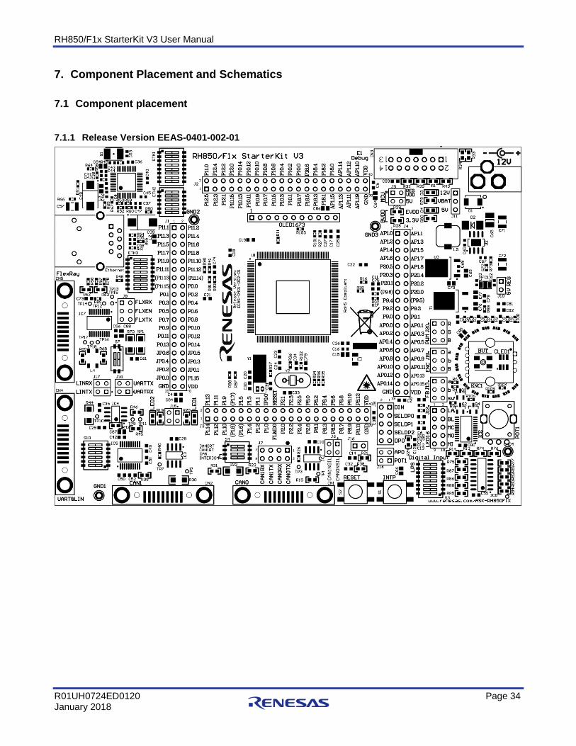
7. Component Placement and Schematics
7.1 Component placement
7.1.1 Release Version EEAS-0401-002-01
RH850/F1x StarterKit V3 User Manual
R01UH0724ED0120 Page 35 January 2018
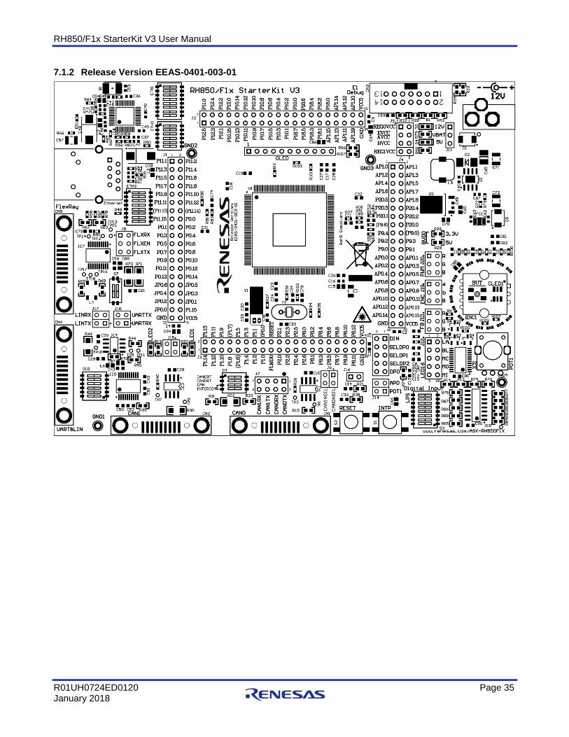
7.1.2 Release Version EEAS-0401-003-01
RH850/F1x StarterKit V3 User Manual
R01UH0724ED0120 Page 36 January 2018
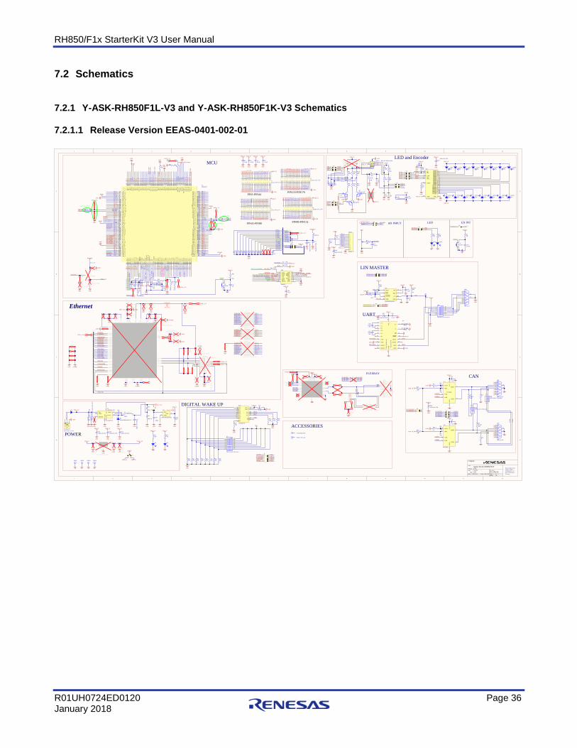
7.2 Schematics
7.2.1 Y-ASK-RH850F1L-V3 and Y-ASK-RH850F1K-V3 Schematics
7.2.1.1 Release Version EEAS-0401-002-01
1
1
2
2
3
3
4
4
5
5
6
6
7
7
8
8
9
9
10
10
11
11
12
12
D D
C C
B B
A A
1
Renesas ElectronicsEurop e GmbHArcadiastrasse 1040472 DüsseldorfGermany122.06.2016 08:35:39
Title
Size Number
Date:
Revision
Sheet ofTime:A1
Starter Kit For RH850/F1X
2.0
HS
Company
Author
Variant F1L
0R17
For F1L/F1H/F1K
P10_
0P1
0_1
P10_
2
P10_3P10_4P10_5
P10_
6P1
0_7
P10_
8P1
0_9
P10_
10P1
0_11
P10_
12P1
0_13
P10_
14
P10_15P11_0
P11_
1P1
1_2
P11_
3P1
1_4
P11_
5P1
1_6
P11_
7
P11_8P11_9P11_10P11_11P11_12
P11_13P11_14
P11_
15P1
2_0
P12_
1P1
2_2
P12_3P12_4P12_5P0_0P0_1P0_2P0_3
P0_4P0_5P0_6
P0_7
P0_8
P0_9
P0_1
0
P0_11P0_12P0_13P0_14
P0_1
5
P1_0P1_1P1_2P1_3
P1_4
P1_5
P1_6
P1_7
P1_8
P1_9
P1_1
0P1
_11
P1_12P1_13
P1_1
4P1
_15
P2_0
P2_1
P2_2
P2_3
P2_4
P2_5
P2_6
P8_0
P8_1
P8_3
P8_2
P8_4
P8_5
P8_6
P8_7
P8_8
P8_9
P8_10P8_11P8_12
JP0_
0JP
0_1
JP0_
2
JP0_3JP0_4JP0_5
IP0_
0
AP0_0AP0_1AP0_2AP0_3AP0_4AP0_5AP0_6AP0_7AP0_8AP0_9AP0_10AP0_11AP0_12AP0_13AP0_14AP0_15
P9_0P9_1P9_2P9_3P9_4
P9_5P9_6
P20_0P20_1P20_2P20_3
P20_4P20_5
AP1
_0AP1_1AP1_2AP1_3AP1_4AP1_5AP1_6AP1_7AP1_8AP1_9AP1_10AP1_11
AP1
_12
AP1
_13
AP1
_14
AP1
_15
P18_
0P1
8_1
P18_
2P1
8_3
P18_
4P1
8_5
P18_
6P1
8_7
MCU
RESET
FLMD0
DCUTDI_FLCS0SI_FLUR0RXDCUTDO_FLCS0SO_FLUR0TX
DCUTCK_FLCS0SCI
DCUTMS
DCUTRST
DCURDY
DC
UT
DI_
FLC
S0SI
_FL
UR
0RX
DC
UT
DO
_FL
CS0
SO_F
LU
R0T
XD
CU
TC
K_F
LC
S0SC
I
DCUTMS
DCURDYDCUTRST
FLM
D0
RE
SET
5K6
R38
1nFC32S2
SPST-NO
VDD_5V
RESET
100K
R43
BVSS
EVSS
EV
DD
1
AW
0VSS
AW
0VD
DR
EG
VD
D
EV
SS
A0VSSA0VREF
EVSS
EVDD2
A1V
RE
FA
1VSS
BV
DD
1IS
0VD
D3
IS0V
SS3
BVDD
EVDDEVDD1EVDD2AW0VDDREGVDDA0VREFA1VREF
BVDD1
IS0VDD0
GND
GND
BV
DD
2B
VSS
GND
BVDD
EVDD
EVDD1 AW0VDD
REGVDD
GND
A0VREF
A1VREFBVDD1BVDD2
BVDD
EVDD
EVDD2
BV
SS
GND
GNDGND
47KR81
47KR82
47KR83
47KR84
47KR88
47KR86
47KR85
47KR87
DIGITAL WAKE UP
GND
DPO
0.1uF
C27
0.1uF
C26
0.1uF
C20
0.1uF
C24
0.1uF
C23
0.1uF
C22
0.1uF
C21
0.1uF
C25
0.1uF
C19
0.1uF
C18
GND
1 216MHzY2
10pFC34
10pFC33
X1
X2
X1X2
0.1uF
C59
GND
10KR77
GND
DIN
DIN_CDIN_BDIN_AI31 I22 I13 I04
Y 5
Y 6
E7
GND 8
S2 9S1 10S0 11
I712 I613 I514 I415
VCC 16IC8
CD74HC151
10KR76
10KR74
10KR75
GND
XT1 XT2
10pFC30
10pFC31
1 232.768kHzY1
XT
1
100K
R37
0
R36 TCK1 GND 2
TRST3 FPMD0 4
TDO5 FPMD1 6
TDI7 VDD 8
TMS9 RESET 10
RDY11 GND 12
RESET13 GND 14
CN3
Flash E1
TCK_FSCI
TRSTTDO_FTXSOTDI_FSIRXTMSTRDYFLDBG_RESET
FLDBG_FLMD0
GND
GND
VDD_5V
10KR32VDD_5V
10KR1
0.1uF
C17
BVDD2
VDD_MCU
M_SELDP2M_SELDP1M_SELDP0
M_D
IN0
M_RX0_RS232M_TX0_RS232
M_R
X1_
LIN
M_T
X1_
LIN
M_CANRX0
M_CANTX1M_CANRX1M_CANTX0
M_A
DC
A1I
0
BP1BM1INH2 1INH1 2EN3
VIO
4
TXD5
TXEN6
RXD7
BG
E8
STBN9
TRXD1 10TRXD0 11
RXEN12 ERRN13
VB
AT
14
WAKE15
GN
D16
BM 17
BP 18
VC
C19
VB
UF
20
IC7TJA1080
0.1uF
C56
4700pF50V
C61
0
R68
0
R69
FR_TXD
FR_RXDFR_TXEZ
VDD_5VVBATF
51R250mW
R7051R250mW
R71
L4
0R63
BVDD
TP12
0R62
TP14TP16
123456
J8
FR_TXD
FR_RXDFR_TXEZ
M_FR_TXD
M_FR_RXDM_FR_TXEZ
M_F
R_T
XD
M_F
R_R
XD
M_F
R_T
XE
Z
GND
GND
BVDDBVDD1BVDD2EVDDEVDD1EVDD2
VDD_MCU REGVDD
A0VREFA1VREF
VDD_5V
FLEXRAY
12345678 9
10111213141516
S3
DIP Switch, 8 Position
VDD_5V
FL_C
ON
1FL
_CO
N2
S_FL
_CO
N1
S_FL
_CO
N2
FLMD1
1 23 4J5
M_APOM_DPO
M_LED1
M_I
NT
P12
POT1
APO
10KR21
S1SPST-NO
VDD_5V
0.01uFC14
INTP12
390RR19
A1
K2
LED2
390RR20
LED1
AD INPUT LED EX INT
GND
0.01uFC12
ADCA0I0S
LED and Encoder
GND
39RR106
1nFC9
10nFC8
10KR14
100RR6
39RR104
10KR13
1.8KR80
5.6KR79
D3 D4
VDD_5V
POWER
VBATF
VDD_5V
VDD_12V
1 32
J11
VDD_12V VDD_5V
TP13TP15
TP17
TP18
1 23 45 67 89 10
J9 DINDIN_ADIN_BDIN_CM_SELDP2
M_SELDP1M_SELDP0M_DIN0
DPOM_DPO
ADCA0I0SM_ADCA0I0SAPOM_APO
1 23 4
J151 2J16
LED1M_LED1LED2M_LED2
M_INTP12 INTP12
0R39
12
34
56
78
910
1112
1314
1516
1718
1920
2122
2324
2526
2728
2930
3132
3334
3536
3738
3940
J4Jumper 20*2 2.54
12
34
56
78
910
111 2
1314
1516
1718
1920
2122
2324
2526
272 8
2930
3132
3334
3536
3738
3940
J2Jumper 20*2 2.54
12
34
56
78
910
1112
1314
1516
1718
1920
2122
2324
2526
2728
2930
3132
3334
3536
3738
3940
J1Jumper 20*2 2.5 4
12
34
56
78
910
1112
1314
1516
1718
1920
2122
2324
2526
2728
2 930
3132
3334
3536
3738
3940
J3Jumper 20*2 2.5 4
GND
VDD_5V
AP0
_0A
P0_ 1
AP0
_2A
P0_3
AP0
_4A
P0_5
AP0
_6A
P0_7
AP0
_8A
P0_9
AP0
_10
AP0
_11
AP0
_12
AP0
_13
AP0
_ 14
AP0
_15
P9_0
P9_1
P9_2
P9_3
P9_4
P9_5
P9_6
P20_
0P2
0_1
P20_
2P2
0_3
P20_
4P2
0_5
AP1
_0A
P1_1
AP1
_2A
P1_3
AP1
_4A
P1_ 5
AP1
_6A
P1_7
AP1
_8
GND
VDD_5V
AP1
_9A
P1_1
0A
P1_1
1A
P1_1
2A
P1_1
3A
P1_1
4A
P1_1
5P1
8_0
P18_
1P1
8_2
P18_
3P1
8_4
P18_
5P1
8_6
P18_
7P1
0_0
P10_
1P1
0_2
P10_
3P1
0_4
P10_
5P1
0_6
P10_
7P1
0_8
P10_
9P1
0_10
P10_
11P1
0_12
P10_
13P1
0_14
P10_
15P1
2_0
P12_
1P1
2_2
P12_
3P1
2_4
P12_
5P1
1_0
GND
VDD_5V
P11_
1P1
1_2
P11_
3P1
1_4
P11_
5P1
1_6
P11_
7P1
1_8
P11_
9P1
1_10
P11_
11P1
1_12
P11_
13P1
1_14
P11_
15P0
_0P0
_1P0
_2P0
_3P0
_4P0
_5P0
_6P0
_7P0
_8P0
_9P0
_10
P0_1
1P0
_12
P0_1
3P0
_14
P0_1
5
JP0_
0JP
0_1
JP0_
2JP
0_3
JP0_
4JP
0_5
P1_1
5
P1_0
P1_1
P1_2
P1_3
P1_4
P1_5
P1_6
P1_7
P1_8
P1_9
P1_1
0P1
_11
P1_1
2P1
_13
P1_1
4
IP0_
0FL
MD
0R
ESE
TP2
_0P2
_1P2
_2P2
_3P2
_4P2
_5P2
_6P8
_0P8
_1P8
_2P 8
_3P8
_4P8
_5P8
_6P8
_7P8
_8P8
_9P8
_10
P8_1
1P8
_12
GND
VDD_5V
M_L
ED
2
M_ADCA0I0S
10K
R24
GND 5
LIN 6
BAT 7
INH 8
TXD4
RXD1
SLP2
WAKE3
IC4
TJA1020/TJA1021
0.1uFC29
LIN1
RX1_LIN
TX1_LIN
VBATF
VDD_5V
VBATF VBATF
VBATF
VDD_5V
10KR42
1nFC35
LIN MASTER1 23 4J17 RX1_LIN
TX1_LINM_RX1_LINM_TX1_LIN
250mW
1K
R44
1KR451KR46
RTX0
RRX0
TX0_RS232
RX0_RS232
47nF16V
C49
VDD_5V
0.1uF
C42VDD_5V
330nF16V
C52
330nF16V
C50
330nF16V
C51
UART
1 23 4J18 TX0_RS232
RX0_RS232M_TX0_RS232M_RX0_RS232
GND
GND
TP9
TP11
123456 7
89101112
S10
DIP Switch, 6 Position
GND
GND
12
43
S7
DIP Switch, 2 Position
M_CANNSIL0
M_CANNSIL1
PIN45-PIN88 PIN89-PIN132
PIN133-PIN176PIN1-PIN44
TP10
TDI_FSIRX
C1+2
C1-4
C2+5
C2-6
V+ 3
V- 7
T1IN13
T2IN12
R1OUT15
R2OUT10 GN
D18
VC
C19
R2IN 9
R1IN 16
T2OUT 8
T1OUT 17
TT
L/C
MO
SL
evel
RS2
32L
evel
EN 1
SHDN 20NC11
NC14
2342332
IC5
FLM
D1
GND
0R16
10nFC11
0
R18 For F1M/F1H
TRST 10KR33GND
100RR34
0.1uFC2
0.1uFC3
0.1uFC4
0.1uFC5
GND GND GND GND
VDD_5V VDD_5V VDD_5V VDD_5V
GND4GND3GND2GND1
L174279214
10µF
/10V
/X5R
C15
10nF
/X7R
/50V
C16
GND GND
VDD_MCU
Ethernet
ETH0MDCETH0MDIO
ETH0RXCLKETH0RXD0ETH0RXD1ETH0RXD2ETH0RXD3
ETH0RXDV
ETH0RXERR
ETH0TXEN
ETH0TXCLK
ETH0TXD0ETH0TXD1ETH0TXD2ETH0TXD3
ETH0TXERR
ETH0CRS
ETH0RESETB
ETH0INT
ETH0COLSD
P10_0P10_1P10_2P10_4P10_5
P11_9P11_10P11_11P11_13P11_14P12_4P12_5
P18_0ETH0LINKP18_1P18_2P18_3P18_4P18_5P18_6P18_7
12345678 9
10111213141516
ETH3
DIP Switch, 8 Position
12345678 9
10111213141516
ETH1
DIP Switch, 8 Position
123456 7
89101112
ETH2
DIP Switch, 6 Position
P11_6
1K
R15
0.1uF
C10
1K
R31
0.1uF
C28
CANTX0
CANRX0
CANTX1
CANRX1
VDD_5V
VDD_5V
CA
NH
CA
NL
250mW120R
R22
250mW120R
R30
TP1
TP5
CAN
CANTX0CANRX0CANTX1CANRX1
M_CANRX0M_CANTX1M_CANRX1
M_CANTX0 1 23 45 67 8
J7
TP3
TP7
3 46 5
S4BDIP Switch, 4 Position
0R23
0R35
1 28 7
S4ADIP Switch, 4 Position1 2
3 4
J6M_CANNSIL0M_CANNSIL1
VDD_5V
VDD_5V
10K
R26
10K
R40
VDD_3.3V
IN3 OUT 4
1
GND
U3
LM1117DT-3.3/NOPB
10nF
/50V
/X7R
C68 C70
10µF
/10V
/X7R
VDD_3.3V
C69
10µF
/10V
/X7R
GNDGND GNDGND
12k4
R67
EX
TR
ES
1
ATP2
P0TXP 3
P0TXN 4
P0A
GN
D1
5
P0RXP 6
P0RXN 7
P0A
GN
D2
8
VD
DA
159
VD
D33
ESD
10
VD
D15
11
P0LINKLED 12
MDC13
MDIO14
INT15
P0RXCLK16
P0RXD317 P0RXD218
VD
DIO
119
GN
DIO
120
P0RXD121 P0RXD022
P0RXDV23
P0RXERR24
P0TXEN25
P0TXD026
P0TXD127
P0TXD228
P0TXD329
P0TXCLK30
VD
DIO
231
XCLK0 32
XCLK1 33
GPIO1434
P0TXERR35
GN
DIO
236
DVOUT1537
VD
DIO
338
P0CRS39
RESETB40
TEST41
P0COLSD42
GN
DA
RE
F43
REGOFF44
AVOUT15 45
VD
DA
33R
EG
46
VD
DA
PLL
47
GN
DA
PLL
48
IC6uPD60610
4k7R65
4k7R47
10pF
C54
10pF
C53
0R0R49
12
25M
Hz
8pF
Digi-Key644-1041-1-ND
Q1
49R9R59
49R9R60
49R9R52
49R9R53
10RR54
10nF/50V/X7RC55
100nF
C41
100nFC36
100nFC40
100nFC45
100nFC44
L3BLM21AG121SN1D
22µF/35V
C48100nFC47
100nFC46
L2
BLM21AG121SN1D
22µF/35VC39
100nFC38
100nFC37
10µF/6.3V/X7RC43
4k7
R48
0R0
R50
0R0
R51
0R0
R55
0R0
R56
10RR61
10nF
/50V
/X7R
C58
220RR57
220RR58
8765
MH
2M
H1
23
1
49101211
J0011D21BNLEthernet
2MR66
2.2n
F/10
00V
/X7R
C574k7R64
GND AGNDEGND
GND
GND
GND
AGNDE
VDD_3.3V GND
GND
AGNDE
AGNDE
GND
VDD_3.3V
GNDGND
VDD_3.3V
AGNDE
VCC3.3_F
ETH0LINK
GND
VDD_3.3V
iNet Class
VDD_3.3V
GND
ETH0MDCETH0MDIO
ETH0RXCLKETH0RXD0ETH0RXD1ETH0RXD2ETH0RXD3ETH0RXDVETH0RXERR
ETH0TXENETH0TXCLKETH0TXD0ETH0TXD1ETH0TXD2ETH0TXD3ETH0TXERR
ETH0CRS
ETH0RESETB
ETH0INT
ETH0COLSD
GND AGNDE
GNDGND
naC67
GND
10nF/50V/X7R
C60 5K23 1%
R72
1K8 1%
R73
GND
GND3 OUT 2VCC1FC1
NFE31PT222Z1E9L
100nF
C62
GNDGND GND
100nFC63
VDD_5V
i Net Class
iNet Class
3,3µ
F/50
VK
eram
ikz.
B.A
VX
C65
GND
Cboot 1
SoftStart2
SYNC3 FB4
ON
5G
ND
6
Vin7
Vswitch 8
U2LM22670-ADJ
D2Diode MBRS240LT3G
10µH
L5
WAKEPWRGND
9-15V (+)-Powe rCon 2.1mm
D1
VD
D_1
2V_I
N
VDD_12V
0R280R29
For F1L/F1K
100µ
F/16
V/X
5R
C72
GND
100µ
F/16
V/X
5RC
71
GND
F1L-002-01
0.1uF
C73
1
2
3
4
5
6
7
8
9
11
10
CN4
DB9 male
1
2
3
4
5
6
7
8
9
11
10
CN5
DB9 male
1
2
3
4
5
6
7
8
9
11
10
CN1
DB9 female
1
2
3
4
5
6
7
8
9
11
10
CN2
DB9 female
12
J10
10kR78
GND
0R0
R89
ACCESSORIESJumperBag 34pc.
Rubber Pads 4pc.
TXD1
GN
D2
RXD4
NSIL5
VC
C3
CANL 6
CANH 7STBY8
IC1
ATA6560
TXD1
GN
D2
RXD4
NSIL5
VC
C3
CANL 6
CANH 7STBY8
IC3
ATA6560
GND
GND
0.1uF
C74
0.1uF
C75
0R900R91
0R41
0R93
GND
IS0VDD0IS0VSS0
VDD_1.2V
IS0VDD2IS0VSS2
0R92
VDD_1.2V
0R27VDD_1.2V
0R98
0R97
EPTVOUT
0R94
IS0V
DD
1IS
0VSS
1
0R95
0R96
VDD_1.2V
IS0VDD3IS0VDD2
T12SD1899
EPTVOUT
10R
R99
1µF 16V X7RC78
GND
10µF/6.3V/X7RC77
10µF/6.3V/X7R
C76
GND
VDD_1.2V
REGVDD
GND
REGVDD
4 2 1
bca
35
ENC1 PEL12T-4225S-S1024
GND 1
SDI2 CLK3
LE4 OUT0 5
OUT1 6
OUT2 7
OUT3 8
OUT4 9
OUT5 10
OUT6 11
OUT7 12
OUT8 13
OUT9 14
OUT10 15
OUT11 16
OUT12 17
OUT13 18
OUT14 19
OUT15 20
OE21
SDO22
R-EXT23
VDD24
IC2
TLC5925IPWRG4
LED3blue
LED4blue
LED5blue
LED6blue
LED7blue
LED8blue
LED9blue
LED10blue
LED18blue
LED17blue
LED16blue
LED15blue
LED14blue
LED13blue
LED12blue
LED11blue
VDD_5V
VDD_5V
VDD_5V
GND
MOSIMISO
MCLK
LAT
VDD_5V
BLNK1 23 45 67 89 10
J12
P0_12P0_13P0_14
P1_14P1_15
Q3
PDTC123JT
Q4PDTC123JT
Q2PDTC123JT
1 23 45 6
J13
123456
J19
1 23 45 6
J20
AP0_3AP0_1
AP0_2
P1_4
P10_9P10_10
P20_2
P20_0P20_1
VDD_5V
GND
GNDGND
GND
VDD_5V GND
10K
R100
10K
R5
GND GND
10nFC1
10K
R310KR2
GND GND
10KR7
10KR8
BVDD
PWM
.R
PWM.G
PWM
.B
FB.RFB.GFB.B
a2
b4
b3
a1
BUT
VDD_5V
1234567891011
OLED
Header 11
VDD_5V
GND
P11_2P11_3P11_0P10_12P11_15P12_1P11_4P11_5AP0_4
10KR11
GND
RED
GR
EEN
BLU
E CLED1RGB LED
1nF
C6
10KR25
1nF
C7
10KR10
1nF
C13
10KR12
GND
0R101
0R102
GND
0.1uF
C79
IS0VDD1
0.1uF
C80
GND
1µF 16V X7RC81
0.1uFC82
GND
BVDD
0.1uFC83
GND
VDD_5V
47KR103
BVDD
1 23 4
J14
47RR9
47RR4
47RR105
P10_31
P10_42
P10_53
BVCC4
BVSS5
P10_156
P11_07
P11_88
P11_99
P11_1010
P11_1111
P11_1212
P11_1313
P11_1414
P12_315
P12_416
P12_517
P0_018
P0_119
P0_220
P0_321
EVCC22
P0_423
P0_524
P0_625
P0_1126
P0_1227
P0_1328
P0_1429
P1_030
P1_131
P1_232
P1_333
P1_1234
P1_1335
P2_636
EVSS37
P8_238
P8_1039
P8_1140
P8_1241
JP0_542
JP0_443
JP0_344
JP0_
245
JP0_
146
JP0_
047
P2_1
48
P2_0
49
P1_1
150
P1_1
051
P1_9
52
P1_8
53
RE
SET
54
EV
CC
55
XT
156
IP0_
057
AW
OV
SS58
AW
OV
CL
59
RE
GV
CC
60
X2
61
X1
62
FLM
D0
63
P2_3
64
P2_2
65
JP0_
666
P0_1
067
P0_9
68
P0_8
69
P0_7
70
EV
SS71
P1_7
72
P1_6
73
P1_5
74
P1_4
75
P2_4
76
P2_5
77
P1_1
478
P1_1
579
P8_0
80
P8_1
81
P8_3
82
P8_4
83
P8_5
84
P8_6
85
P8_7
86
P8_8
87
P8_9
88
A0VSS 89A0VREF 90AP0_15 91AP0_14 92AP0_13 93AP0_12 94AP0_11 95AP0_10 96AP0_9 97AP0_8 98AP0_7 99AP0_6 100AP0_5 101AP0_4 102AP0_3 103AP0_2 104AP0_1 105AP0_0 106EVSS 107P9_0 108P9_1 109P9_2 110P9_3 111P9_4 112P9_5 113P9_6 114P20_3 115P20_2 116P20_1 117P20_0 118P20_5 119P20_4 120EVCC 121AP1_11 122AP1_10 123AP1_9 124AP1_8 125AP1_7 126AP1_6 127AP1_5 128AP1_4 129AP1_3 130AP1_2 131AP1_1 132A
P1_0
133
AP1
_15
134
AP1
_14
135
AP1
_13
136
AP1
_12
137
A1V
RE
VF
138
A1V
SS13
9B
VC
C14
0IS
OV
CL
141
ISO
VSS
142
P18_
014
3P1
8_1
144
P18_
214
5P1
8_3
146
P18_
414
7P1
8_5
148
P18_
614
9P1
8_7
150
BV
SS15
1P1
0_6
152
P10_
715
3P1
0_8
154
P10_
915
5P1
0_10
156
P10_
1115
7P1
0_12
158
P10_
1315
9P1
0_14
160
P11_
116
1P1
1_2
162
P11_
316
3P1
1_4
164
P11_
516
5P1
1_6
166
P11_
716
7P1
1_15
168
P12_
016
9P1
2_1
170
P12_
217
1B
VC
C17
2B
VSS
173
P10_
017
4P1
0_1
175
P10_
217
6
U1RH850F1L
C87
10µF/10V/X7RGND
C8810µF/10V/X7R
GND
VDD_5V
C8610µF/10V/X7R
GND
VDD_5V
C6410µF/10V/X7R
GND
VDD_5V
C6610µF/10V/X7R
GND
VDD_5V
C8410µF/10V/X7R
GND
VDD_5V
C8510µF/10V/X7R
GND
VDD_5V
RH850/F1x StarterKit V3 User Manual
R01UH0724ED0120 Page 37 January 2018
7.2.1.2 Release Version EEAS-0401-003-01
1
1
2
2
3
3
4
4
5
5
6
6
7
7
8
8
9
9
10
10
11
11
12
12
D D
C C
B B
A A
1
Renesas ElectronicsEurop e GmbHArcadiastrasse 1040472 DüsseldorfGermany107.02.2017 15:05:07
Title
Size Number
Date:
Revision
Sheet ofTime:A1
Starter Kit For RH850/F1X
2.0
HS
Company
Author
Variant F1L/F1K
0R17
P10_
0P1
0_1
P10_
2
P10_3P10_4P10_5
P10_
6P1
0_7
P10_
8P1
0_9
P10_
10P1
0_11
P10_
12P1
0_13
P10_
14
P10_15P11_0
P11_
1P1
1_2
P11_
3P1
1_4
P11_
5P1
1_6
P11_
7
P11_8P11_9P11_10P11_11P11_12
P11_13P11_14
P11_
15P1
2_0
P12_
1P1
2_2
P12_3P12_4P12_5P0_0P0_1P0_2P0_3
P0_4P0_5P0_6
P0_7
P0_8
P0_9
P0_1
0P0_11P0_12P0_13P0_14
JP0_
6
P1_0P1_1P1_2P1_3
P1_4
P1_5
P1_6
P1_7
P1_8
P1_9
P1_1
0P1
_11
P1_12P1_13
P1_1
4P1
_15
P2_0
P2_1
P2_2
P2_3
P2_4
P2_5
P2_6
P8_0
P8_1
P8_3
P8_2
P8_4
P8_5
P8_6
P8_7
P8_8
P8_9
P8_10P8_11P8_12
JP0_
0JP
0_1
JP0_
2
JP0_3JP0_4JP0_5
IP0_
0
AP0_0AP0_1AP0_2AP0_3AP0_4AP0_5AP0_6AP0_7AP0_8AP0_9AP0_10AP0_11AP0_12AP0_13AP0_14AP0_15
P9_0P9_1P9_2P9_3
P9_4P9_5P9_6
P20_0P20_1P20_2P20_3
P20_4P20_5
AP1
_0
AP1_1AP1_2AP1_3AP1_4AP1_5AP1_6AP1_7AP1_8AP1_9AP1_10AP1_11
AP1
_12
AP1
_13
AP1
_14
AP1
_15
P18_
0P1
8_1
P18_
2P1
8_3
P18_
4P1
8_5
P18_
6P1
8_7
MCU
RESET
FLMD0
DCUTDI_FLCS0SI_FLUR0RXDCUTDO_FLCS0SO_FLUR0TX
DCUTCK_FLCS0SCI
DCUTMS
DCUTRST
DCURDY
DC
UT
DI_
FLC
S0SI
_FL
UR
0RX
DC
UT
DO
_FL
CS0
SO_F
LU
R0T
XD
CU
TC
K_F
LC
S0SC
I
DCUTMS
DCURDYDCUTRST
FLM
D0
RE
SET
5K6
R38
1nFC32S2
SPST-NO
VDD_5V
RESET
100K
R43
BVSS
EVSS
EV
CC
1
AW
0VSS
AW
OV
CL
RE
G0V
CC
EV
SS
A0VSSA0VREF
EVSS
EVCC2
A1V
RE
FA
1VSS
BV
CC
1IS
OV
CL
3IS
0VSS
3
BVCC
EVCCEVCC1EVCC2AWOVCLREG0VCCA0VREFA1VREF
BVCC1
ISOVCL0
GND
GNDB
VC
C2
BV
SS
GND
BVCC
EVCC
EVCC1 AWOVCL
REG0VCC
GND
A0VREF
A1VREFBVCC1BVCC2
BVCC
EVCC
EVCC2
BV
SS
GND
GNDGND
47KR81
47KR82
47KR83
47KR84
47KR88
47KR86
47KR85
47KR87
DIGITAL WAKE UP
GND
DPO
0.1uF
C27
0.1uF
C26
0.1uF
C20
0.1uF
C24
0.1uF
C23
0.1uF
C22
0.1uF
C21
0.1uF
C25
0.1uF
C19
0.1uF
C18
GND
1 216MHzY2
10pFC34
10pFC33
X1
X2
X1X2
0.1uF
C59
GND
10KR77
GND
DIN
DIN_CDIN_BDIN_AI31 I22 I13 I04
Y 5
Y 6
E7
GND 8
S2 9S1 10S0 11
I712 I613 I514 I415
VCC 16IC8
CD74HC151
10KR76
10KR74
10KR75
GND
XT1 XT2
10pFC30
10pFC31
1 232.768kHzY1
XT
1
100K
R37
0
R36 TCK1 GND 2
TRST3 FPMD0 4
TDO5 FPMD1 6
TDI7 VDD 8
TMS9 RESET 10
RDY11 GND 12
RESET13 GND 14
CN3
Flash E1
TCK_FSCI
TRSTTDO_FTXSOTDI_FSIRXTMSTRDYFLDBG_RESET
FLDBG_FLMD0
GND
GND
VDD_5V
10KR32VDD_5V
10KR1
0.1uF
C17
BVCC2
M_SELDP2M_SELDP1M_SELDP0
M_D
IN0
M_RX0_RS232M_TX0_RS232
M_R
X1_
LIN
M_T
X1_
LIN
M_CANRX0
M_CANTX1M_CANRX1M_CANTX0
M_A
DC
A1I
0
BP1BM1INH2 1INH1 2EN3
VIO
4
TXD5
TXEN6
RXD7
BG
E8
STBN9
TRXD1 10TRXD0 11
RXEN12 ERRN13
VB
AT
14
WAKE15
GN
D16
BM 17
BP 18
VC
C19
VB
UF
20IC7TJA1080
0.1uF
C56
4700pF50V
C61
0
R68
0
R69
FR_TXD
FR_RXDFR_TXEZ
VDD_5VVBATF
51R250mW
R7051R250mW
R71
L4
0R63
BVCC
TP12
0R62
TP14TP16
123456
J8
FR_TXD
FR_RXDFR_TXEZ
M_FR_TXD
M_FR_RXDM_FR_TXEZ
M_F
R_T
XD
M_F
R_R
XD
M_F
R_T
XE
Z
GND
GND
BVCCBVCC1BVCC2
EVCCEVCC1EVCC2
REG0VCC
A0VREFA1VREF
VDD_5V
FLEXRAY
12345678 9
10111213141516
S3
DIP Switch, 8 Position
VDD_5V
FL_C
ON
1FL
_CO
N2
S_FL
_CO
N1
S_FL
_CO
N2
FLMD1
M_APOM_DPO
M_LED1M
_IN
TP1
2
POT1
APO
10KR21
S1SPST-NO
VDD_5V
0.01uFC14
INTP12
390RR19
A1
K2
LED2
390RR20
LED1
AD INPUT LED EX INT
GND
0.01uFC12
ADCA0I0S
LED and Encoder
GND
39RR106
1nFC9
10nFC8
10KR14
100RR6
39RR104
10KR13
1.8KR80
5.6KR79
D3 D4
VDD_5V
POWER
VBATF
VDD_5V
VDD_12V
1 32
J11
VDD_12V VDD_5V
TP13TP15
TP17
TP18
1 23 45 67 89 10
J9 DINDIN_ADIN_BDIN_CM_SELDP2
M_SELDP1M_SELDP0M_DIN0
DPOM_DPO
ADCA0I0SM_ADCA0I0SAPOM_APO
1 23 4
J151 2J16
LED1M_LED1LED2M_LED2
M_INTP12 INTP12
0R39
12
34
56
78
910
1112
1314
1516
1718
1920
2122
2324
2526
2728
2930
3132
3334
3536
3738
3940
J4Jumper 20x2
12
34
56
78
910
111 2
1314
1516
1718
1920
2122
2324
2526
272 8
2930
3132
3334
3536
3738
3940
J2Jumper 20x2
12
34
56
78
910
1112
1314
1516
1718
1920
2122
2324
2526
2728
2930
3132
3 334
3536
3738
3940
J1Jumper 20x2
12
34
56
78
910
1112
1314
1516
1718
1920
2122
2324
2526
2728
2 930
3132
3334
3536
3738
3940
J3Jumper 20x2
GND
VDD_5V
AP0
_0A
P0_ 1
AP0
_2A
P0_3
AP0
_4A
P0_5
AP0
_6A
P0_7
AP0
_8A
P0_9
AP0
_10
AP0
_11
AP0
_12
AP0
_13
AP0
_ 14
AP0
_15
P9_0
P9_1
P9_2
P9_3
P9_4
P9_5
P9_6
P20_
0P2
0_1
P20_
2P2
0_3
P20_
4P2
0_5
AP1
_0A
P1_1
AP1
_2A
P1_3
AP1
_4A
P1_ 5
AP1
_6A
P1_7
AP1
_8
GND
VDD_5V
AP1
_9A
P1_1
0A
P1_1
1A
P1_1
2A
P1_1
3A
P1_1
4A
P1_1
5P1
8_0
P18_
1P1
8_2
P18_
3P1
8_4
P18_
5P1
8_6
P18_
7P1
0_0
P10_
1P1
0_2
P10_
3P1
0_4
P10_
5P1
0_6
P10_
7P1
0_8
P10_
9P1
0_10
P10_
11P1
0_12
P10_
13P1
0_14
P10_
15P1
2_0
P12_
1P1
2_2
P12_
3P1
2_4
P12_
5P1
1_0
GND
VDD_5V
P11_
1P1
1_2
P11_
3P1
1_4
P11_
5P1
1_6
P11_
7P1
1_8
P11_
9P1
1_10
P11_
11P1
1_12
P11_
13P1
1_14
P11_
15P0
_0P0
_1P0
_2P0
_3P0
_4P0
_5P0
_6P0
_7P0
_8P0
_9P0
_10
P0_1
1P0
_12
P0_1
3P0
_14
JP0_
6
JP0_
0JP
0_1
JP0_
2J P
0_3
JP0_
4JP
0_5
P1_1
5
P1_0
P1_1
P1_2
P1_3
P1_4
P1_5
P1_6
P1_7
P1_8
P1_9
P1_1
0P1
_11
P1_1
2P1
_13
P1_1
4
IP0_
0FL
MD
0R
ESE
TP2
_0P2
_1P2
_2P2
_3P2
_4P2
_5P2
_6P8
_0P8
_1P8
_2P 8
_3P8
_4P8
_5P8
_6P8
_7P8
_8P8
_9P8
_10
P8_1
1P8
_12
GND
VDD_5V
M_L
ED
2
M_ADCA0I0S
10K
R24
GND 5
LIN 6
BAT 7
INH 8
TXD4
RXD1
SLP2
WAKE3
IC4
TJA1020/TJA1021
0.1uFC29
LIN1
RX1_LIN
TX1_LIN
VBATF
VDD_5V
VBATF VBATF
VBATF
VDD_5V
10KR42
1nFC35
LIN MASTER1 23 4J17 RX1_LIN
TX1_LINM_RX1_LINM_TX1_LIN
250mW
1K
R44
1KR451KR46
RTX0
RRX0
TX0_RS232
RX0_RS232
47nF16V
C49
0.1uF
C42
VDD_5V
330nF16V
C52
330nF16V
C50
330nF16V
C51
UART
1 23 4J18 TX0_RS232
RX0_RS232M_TX0_RS232M_RX0_RS232
GND
GND
TP9
TP11
123456 7
89101112
S10
DIP Switch, 6 Position
GND
GND
12
43
S7
DIP Switch, 2 Position
M_CANNSIL0
M_CANNSIL1
PIN45-PIN88 PIN89-PIN132
PIN133-PIN176PIN1-PIN44
TP10
TDI_FSIRX
C1+2
C1-4
C2+5
C2-6
V+ 3
V- 7
T1IN13
T2IN12
R1OUT15
R2OUT10 GN
D18
VC
C19
R2IN 9
R1IN 16
T2OUT 8
T1OUT 17
TT
L/C
MO
SL
evel
RS2
32L
evel
EN 1
SHDN 20NC11
NC14
IC5
FLM
D1
GND
0R16
0.1uF
C11
0
R18
TRST 10KR33GND
100RR34
0.1uFC2
0.1uFC3
0.1uFC4
0.1uFC5
GND GND GND GND
VDD_5V VDD_5V VDD_5V VDD_5V
GND4GND3GND2GND1
L174279214
10µF
/10V
/X5R
C15
10nF
/X7R
/50V
C16
GND GND
Ethernet
ETH0MDCETH0MDIO
ETH0RXCLKETH0RXD0ETH0RXD1ETH0RXD2ETH0RXD3
ETH0RXDV
ETH0RXERR
ETH0TXEN
ETH0TXCLK
ETH0TXD0ETH0TXD1ETH0TXD2ETH0TXD3
ETH0TXERR
ETH0CRS
ETH0RESETB
ETH0INT
ETH0COLSD
P10_0P10_1P10_2P10_4P10_5
P11_9P11_10P11_11P11_13P11_14P12_4P12_5
P18_0ETH0LINKP18_1P18_2P18_3P18_4P18_5P18_6P18_7
12345678 9
10111213141516
ETH3
DIP Switch, 8 Position
12345678 9
10111213141516
ETH1
DIP Switch, 8 Position
123456 7
89101112
ETH2
DIP Switch, 6 Position
P11_6
1K
R15
0.1uF
C10
1K
R31
0.1uF
C28
CANTX0
CANRX0
CANTX1
CANRX1
VDD_5V
VDD_5V
CA
NH
CA
NL
250mW120R
R22
250mW120R
R30
TP1
TP5
CAN
CANTX0CANRX0CANTX1CANRX1
M_CANRX0M_CANTX1M_CANRX1
M_CANTX0 1 23 45 67 8
J7
TP3
TP7
3 46 5
S4BDIP Switch, 4 Position
0R23
0R35
1 28 7
S4ADIP Switch, 4 Position1 2
3 4
J6M_CANNSIL0M_CANNSIL1
VDD_5V
VDD_5V
10K
R26
10K
R40
VDD_3.3V
IN3 OUT 4
1
GND
U3
LM1117DT-3.3/NOPB
10nF
/50V
/X7R
C68 C70
10µF
/10V
/X7R
VDD_3.3V
C69
10µF
/10V
/X7R
GNDGND GNDGND
12k4
R67
EX
TR
ES
1
ATP2
P0TXP 3
P0TXN 4
P0A
GN
D1
5
P0RXP 6
P0RXN 7
P0A
GN
D2
8
VD
DA
159
VD
D33
ESD
10
VD
D15
11
P0LINKLED 12
MDC13
MDIO14
INT15
P0RXCLK16
P0RXD317 P0RXD218
VD
DIO
119
GN
DIO
120
P0RXD121 P0RXD022
P0RXDV23
P0RXERR24
P0TXEN25
P0TXD026
P0TXD127
P0TXD228
P0TXD329
P0TXCLK30
VD
DIO
231
XCLK0 32
XCLK1 33
GPIO1434
P0TXERR35
GN
DIO
236
DVOUT1537
VD
DIO
338
P0CRS39
RESETB40
TEST41
P0COLSD42
GN
DA
RE
F43
REGOFF44
AVOUT15 45
VD
DA
33R
EG
46
VD
DA
PLL
47
GN
DA
PLL
48
IC6uPD60610
4k7R65
4k7R47
10pF
C54
10pF
C53
0R0R49
12
25M
Hz
8pF
Digi-Key644-1041-1-ND
Q1
49R9R59
49R9R60
49R9R52
49R9R53
10RR54
10nF/50V/X7RC55
100nF
C41
100nFC36
100nFC40
100nFC45
100nFC44
L3BLM21AG121SN1D
22µF/35V
C48100nFC47
100nFC46
L2
BLM21AG121SN1D
22µF/35VC39
100nFC38
100nFC37
10µF/6.3V/X7RC43
4k7
R48
0R0
R50
0R0
R51
0R0
R55
0R0
R56
10RR61
10nF
/50V
/X7R
C58
220RR57
220RR58
8765
MH
2M
H1
23
1
49101211
J0011D21BNLEthernet
2MR66
2.2n
F/10
00V
/X7R
C574k7R64
GND AGNDEGND
GND
GND
GND
AGNDE
VDD_3.3V GND
GND
AGNDE
AGNDE
GND
VDD_3.3V
GNDGND
VDD_3.3V
AGNDE
VCC3.3_F
ETH0LINK
GND
VDD_3.3V
iNet Class
VDD_3.3V
GND
ETH0MDCETH0MDIO
ETH0RXCLKETH0RXD0ETH0RXD1ETH0RXD2ETH0RXD3ETH0RXDVETH0RXERR
ETH0TXENETH0TXCLKETH0TXD0ETH0TXD1ETH0TXD2ETH0TXD3ETH0TXERR
ETH0CRS
ETH0RESETB
ETH0INT
ETH0COLSD
GND AGNDE
GNDGND
naC67
GND
10nF/50V/X7R
C60 5K23 1%
R72
1K64 1%
R73
GND
GND3 OUT 2VCC1FC1
NFE31PT222Z1E9L
100nF
C62
GNDGND GND
100nFC63
VDD_5V
i Net Class
iNet Class
3,3µ
F/50
VK
eram
ikz.
B.A
VX
C65
GND
Cboot 1
SoftStart2
SYNC3 FB4
ON
5G
ND
6
Vin7
Vswitch 8
U2LM22670-ADJ
D2Diode MBRS240LT3G
10µH
L5
WAKEPWRGND
9-15V (+)-Powe rCon 2.1mm
D1
VD
D_1
2V_I
N
VDD_12V
0R28
0R29
100µ
F/16
V/X
5R
C72
GND
100µ
F/16
V/X
5RC
71
GND
F1L-003-01
0.1uF
C73
1
2
3
4
5
6
7
8
9
11
10
CN4
DB9 male
1
2
3
4
5
6
7
8
9
11
10
CN5
DB9 male
1
2
3
4
5
6
7
8
9
11
10
CN1
DB9 female
1
2
3
4
5
6
7
8
9
11
10
CN2
DB9 female
10kR78
GND
0R0
R89
ACCESSORIESJumperBag 34pc.
Rubber Pads 4pc.
TXD1
GN
D2
RXD4
NSIL5
VC
C3
CANL 6
CANH 7STBY8
IC1
ATA6560
TXD1
GN
D2
RXD4
NSIL5
VC
C3
CANL 6
CANH 7STBY8
IC3
ATA6560
GND
GND
0.1uF
C74
0.1uF
C75
0R900R91
0R93
GND
ISOVCL0IS0VSS0
ISOVCL2IS0VSS2
0
R92
0R94
ISO
VC
L1
IS0V
SS1
0R95
ISOVCL3ISOVCL2
4 2 1
bca
35
ENC1 PEL12T-4225S-S1024
GND 1
SDI2 CLK3
LE4 OUT0 5
OUT1 6
OUT2 7
OUT3 8
OUT4 9
OUT5 10
OUT6 11
OUT7 12
OUT8 13
OUT9 14
OUT10 15
OUT11 16
OUT12 17
OUT13 18
OUT14 19
OUT15 20
OE21
SDO22
R-EXT23
VDD24
IC2
TLC5925IPWRG4
LED3LED Blue
LED4LED Blue
LED5LED Blue
LED6LED Blue
LED7LED Blue
LED8LED Blue
LED9LED Blue
LED10LED Blue
LED18LED Blue
LED17LED Blue
LED16LED Blue
LED15LED Blue
LED14LED Blue
LED13LED Blue
LED12LED Blue
LED11LED Blue
VDD_5V
VDD_5V
VDD_5V
GND
MOSIMISO
MCLK
LAT
VDD_5V
BLNK1 23 45 67 89 10
J12
P0_12P0_13P0_14
P1_14P1_15
Q3
PDTC123JT
Q4PDTC123JT
Q2PDTC123JT
1 23 45 6
J13
123456
J19
1 23 45 6
J20
AP0_3AP0_1
AP0_2
P1_4
P10_9P10_10
P20_2
P20_0P20_1
VDD_5V
GND
GNDGND
GND
VDD_5V GND
10K
R100
10K
R5
GND GND
10nFC1
10K
R310KR2
GND GND
10KR7
10KR8
BVCC
PWM
.R
PWM.G
PWM
.B
FB.RFB.GFB.B
a2
b4
b3
a1
BUT
VDD_5V
1234567891011
OLED
Header 11
VDD_5V
GND
P11_2P11_3P11_0P10_12P11_15P12_1P11_4P11_5AP0_4
10KR11
GND
RED
GR
EEN
BLU
E CLED1RGB LED
1nF
C6
10KR25
1nF
C7
10KR10
1nF
C13
10KR12
GND
0R101
0R102
GND
0.1uF
C79
ISOVCL1
0.1uF
C80
GND
1µF 16V X7RC81
0.1uFC82
GND
BVCC
0.1uFC83
GND
VDD_5V
47KR103
BVCC
1 23 4
J14
47RR9
47RR4
47RR105
P10_31
P10_42
P10_53
BVCC4
BVSS5
P10_156
P11_07
P11_88
P11_99
P11_1010
P11_1111
P11_1212
P11_1313
P11_1414
P12_315
P12_416
P12_517
P0_018
P0_119
P0_220
P0_321
EVCC22
P0_423
P0_524
P0_625
P0_1126
P0_1227
P0_1328
P0_1429
P1_030
P1_131
P1_232
P1_333
P1_1234
P1_1335
P2_636
EVSS37
P8_238
P8_1039
P8_1140
P8_1241
JP0_542
JP0_443
JP0_344
JP0_
245
JP0_
146
JP0_
047
P2_1
48
P2_0
49
P1_1
150
P1_1
051
P1_9
52
P1_8
53
RE
SET
54
EV
CC
55
XT
156
IP0_
057
AW
OV
SS58
AW
OV
CL
59
RE
GV
CC
60
X2
61
X1
62
FLM
D0
63
P2_3
64
P2_2
65
JP0_
666
P0_1
067
P0_9
68
P0_8
69
P0_7
70
EV
SS71
P1_7
72
P1_6
73
P1_5
74
P1_4
75
P2_4
76
P2_5
77
P1_1
478
P1_1
579
P8_0
80
P8_1
81
P8_3
82
P8_4
83
P8_5
84
P8_6
85
P8_7
86
P8_8
87
P8_9
88
A0VSS 89A0VREF 90AP0_15 91AP0_14 92AP0_13 93AP0_12 94AP0_11 95AP0_10 96AP0_9 97AP0_8 98AP0_7 99AP0_6 100AP0_5 101AP0_4 102AP0_3 103AP0_2 104AP0_1 105AP0_0 106EVSS 107P9_0 108P9_1 109P9_2 110P9_3 111P9_4 112P9_5 113P9_6 114P20_3 115P20_2 116P20_1 117P20_0 118P20_5 119P20_4 120EVCC 121AP1_11 122AP1_10 123AP1_9 124AP1_8 125AP1_7 126AP1_6 127AP1_5 128AP1_4 129AP1_3 130AP1_2 131AP1_1 132
AP1
_013
3A
P1_1
513
4A
P1_1
413
5A
P1_1
313
6A
P1_1
213
7A
1VR
EV
F13
8A
1VSS
139
BV
CC
140
ISO
VC
L14
1IS
OV
SS14
2P1
8_0
143
P18_
114
4P1
8_2
145
P18_
314
6P1
8_4
147
P18_
514
8P1
8_6
149
P18_
715
0B
VSS
151
P10_
615
2P1
0_7
153
P10_
815
4P1
0_9
155
P10_
1015
6P1
0_11
157
P10_
1215
8P1
0_13
159
P10_
1416
0P1
1_1
161
P11_
216
2P1
1_3
163
P11_
416
4P1
1_5
165
P11_
616
6P1
1_7
167
P11_
1516
8P1
2_0
169
P12_
117
0P1
2_2
171
BV
CC
172
BV
SS17
3P1
0_0
174
P10_
117
5P1
0_2
176
U1RH850
C87
10µF/10V/X7RGND
C8810µF/10V/X7R
GND
VDD_5V
C8610µF/10V/X7R
GND
VDD_5V
C6410µF/10V/X7R
GND
VDD_5V
C6610µF/10V/X7R
GND
VDD_5V
C8410µF/10V/X7R
GND
VDD_5V
C8510µF/10V/X7R
GND
VDD_5V
0R107
10KR96
JP0_6
0.1uF
C890R108
IS0VSS2
ISOx
0R410R27
REG0VCCREG1VCC
1 23 45 6
J5
VDD_5V
VDD_5V VDD_3.3V
EVCCBVCC
REG1VCC
D5
L6
BLM21AG121SN1D
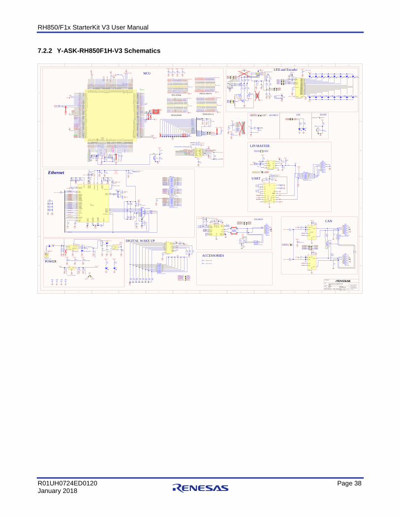
RH850/F1x StarterKit V3 User Manual
R01UH0724ED0120 Page 38 January 2018
7.2.2 Y-ASK-RH850F1H-V3 Schematics
1
1
2
2
3
3
4
4
5
5
6
6
7
7
8
8
9
9
10
10
11
11
12
12
D D
C C
B B
A A
1
Renesas ElectronicsEurop e GmbHArcadiastrasse 1040472 DüsseldorfGermany107.02.2017 15:05:14
Title
Size Number
Date:
Revision
Sheet ofTime:A1
Starter Kit For RH850/F1X
2.0
HS
Company
Author
Variant F1H
0R17
P10_
0P1
0_1
P10_
2
P10_3P10_4P10_5
P10_
6P1
0_7
P10_
8P1
0_9
P10_
10P1
0_11
P10_
12P1
0_13
P10_
14
P10_15P11_0
P11_
1P1
1_2
P11_
3P1
1_4
P11_
5P1
1_6
P11_
7
P11_8P11_9P11_10P11_11P11_12
P11_13P11_14
P11_
15P1
2_0
P12_
1P1
2_2
P12_3P12_4P12_5P0_0P0_1P0_2P0_3
P0_4P0_5P0_6
P0_7
P0_8
P0_9
P0_1
0
P0_11P0_12P0_13P0_14
JP0_
6
P1_0P1_1P1_2P1_3
P1_4
P1_5
P1_6
P1_7
P1_8
P1_9
P1_1
0P1
_11
P1_12P1_13
P1_1
4P1
_15
P2_0
P2_1
P2_2
P2_3
P2_4
P2_5
P2_6
P8_0
P8_1
P8_3
P8_2
P8_4
P8_5
P8_6
P8_7
P8_8
P8_9
P8_10P8_11P8_12
JP0_
0JP
0_1
JP0_
2
JP0_3JP0_4JP0_5
IP0_
0
AP0_0AP0_1AP0_2AP0_3AP0_4AP0_5AP0_6AP0_7AP0_8AP0_9AP0_10AP0_11AP0_12AP0_13AP0_14AP0_15
P9_0P9_1P9_2P9_3
P9_4P9_5P9_6
P20_0P20_1P20_2P20_3
P20_4P20_5
AP1
_0
AP1_1AP1_2AP1_3AP1_4AP1_5AP1_6AP1_7AP1_8AP1_9AP1_10AP1_11
AP1
_12
AP1
_13
AP1
_14
AP1
_15
P18_
0P1
8_1
P18_
2P1
8_3
P18_
4P1
8_5
P18_
6P1
8_7
MCU
RESET
FLMD0
DCUTDI_FLCS0SI_FLUR0RXDCUTDO_FLCS0SO_FLUR0TX
DCUTCK_FLCS0SCI
DCUTMS
DCUTRST
DCURDY
DC
UT
DI_
FLC
S0SI
_FL
UR
0RX
DC
UT
DO
_FL
CS0
SO_F
LU
R0T
XD
CU
TC
K_F
LC
S0SC
I
DCUTMS
DCURDYDCUTRST
FLM
D0
RE
SET
5K6
R38
1nFC32S2
SPST-NO
VDD_5V
RESET
100K
R43
BVSS
EVSS
EV
CC
1
AW
0VSS
AW
OV
CL
RE
G0V
CC
EV
SS
A0VSSA0VREF
EVSS
EVCC2
A1V
RE
FA
1VSS
BV
CC
1IS
OV
CL
3IS
0VSS
3
BVCC
EVCCEVCC1EVCC2AWOVCLREG0VCCA0VREFA1VREF
BVCC1
ISOVCL0
GND
GND
BV
CC
2B
VSS
GND
BVCC
EVCC
EVCC1 AWOVCL
REG0VCC
GND
A0VREF
A1VREFBVCC1BVCC2
BVCC
EVCC
EVCC2
BV
SS
GND
GNDGND
47KR81
47KR82
47KR83
47KR84
47KR88
47KR86
47KR85
47KR87
DIGITAL WAKE UP
GND
DPO
0.1uF
C27
0.1uF
C26
0.1uF
C20
0.1uF
C24
0.1uF
C23
0.1uF
C22
0.1uF
C21
0.1uF
C25
0.1uF
C19
0.1uF
C18
GND
1 216MHzY2
10pFC34
10pFC33
X1
X2
X1X2
0.1uF
C59
GND
10KR77
GND
DIN
DIN_CDIN_BDIN_AI31 I22 I13 I04
Y 5
Y 6
E7
GND 8
S2 9S1 10S0 11
I712 I613 I514 I415
VCC 16IC8
CD74HC151
10KR76
10KR74
10KR75
GND
XT1 XT2
10pFC30
10pFC31
1 232.768kHzY1
XT
1
100K
R37
0
R36 TCK1 GND 2
TRST3 FPMD0 4
TDO5 FPMD1 6
TDI7 VDD 8
TMS9 RESET 10
RDY11 GND 12
RESET13 GND 14
CN3
Flash E1
TCK_FSCI
TRSTTDO_FTXSOTDI_FSIRXTMSTRDYFLDBG_RESET
FLDBG_FLMD0
GND
GND
VDD_5V
10KR32VDD_5V
10KR1
0.1uF
C17
BVCC2
M_SELDP2M_SELDP1M_SELDP0
M_D
IN0
M_RX0_RS232M_TX0_RS232
M_R
X1_
LIN
M_T
X1_
LIN
M_CANRX0
M_CANTX1M_CANRX1M_CANTX0
M_A
DC
A1I
0
BP1BM1INH2 1INH1 2EN3
VIO
4
TXD5
TXEN6
RXD7
BG
E8
STBN9
TRXD1 10TRXD0 11
RXEN12 ERRN13
VB
AT
14
WAKE15
GN
D16
BM 17
BP 18
VC
C19
VB
UF
20
IC7TJA1080
0.1uF
C56
4700pF50V
C61
0
R68
0
R69
FR_TXD
FR_RXDFR_TXEZ
VDD_5VVBATF
51R250mW
R7051R250mW
R71
L4
0R63
BVCC
TP12
0R62
TP14TP16
123456
J8
FR_TXD
FR_RXDFR_TXEZ
M_FR_TXD
M_FR_RXDM_FR_TXEZ
M_F
R_T
XD
M_F
R_R
XD
M_F
R_T
XE
Z
GND
GND
BVCCBVCC1BVCC2
EVCCEVCC1EVCC2
REG0VCC
A0VREFA1VREF
VDD_5V
FLEXRAY
12345678 9
10111213141516
S3
DIP Switch, 8 Position
VDD_5V
FL_C
ON
1FL
_CO
N2
S_FL
_CO
N1
S_FL
_CO
N2
FLMD1
M_APOM_DPO
M_LED1
M_I
NT
P12
POT1
APO
10KR21
S1SPST-NO
VDD_5V
0.01uFC14
INTP12
390RR19
A1
K2
LED2
390RR20
LED1
AD INPUT LED EX INT
GND
0.01uFC12
ADCA0I0S
LED and Encoder
GND
39RR106
1nFC9
10nFC8
10KR14
100RR6
39RR104
10KR13
1.8KR80
5.6KR79
D3 D4
VDD_5V
POWER
VBATF
VDD_5V
VDD_12V
1 32
J11
VDD_12V VDD_5V
TP13TP15
TP17
TP18
1 23 45 67 89 10
J9 DINDIN_ADIN_BDIN_CM_SELDP2
M_SELDP1M_SELDP0M_DIN0
DPOM_DPO
ADCA0I0SM_ADCA0I0SAPOM_APO
1 23 4
J151 2J16
LED1M_LED1LED2M_LED2
M_INTP12 INTP12
0R39
12
34
56
78
910
1112
1314
1516
1718
1920
2122
2324
2526
2728
2930
3132
3334
3536
3738
3940
J4Jumper 20x2
12
34
56
78
910
111 2
1314
1516
1718
1920
2122
2324
2526
272 8
2930
3132
3334
3536
3738
3940
J2Jumper 20x2
12
34
56
78
910
1112
1314
1516
1718
1920
2122
2324
2526
2728
2930
3132
3 334
3536
3738
3940
J1Jumper 20x2
12
34
56
78
910
1112
1314
1516
1718
1920
2122
2324
2526
2728
2 930
3132
3334
3536
3738
3940
J3Jumper 20x2
GND
VDD_5V
AP0
_0A
P0_ 1
AP0
_2A
P0_3
AP0
_4A
P0_5
AP0
_6A
P0_7
AP0
_8A
P0_9
AP0
_10
AP0
_11
AP0
_12
AP0
_13
AP0
_ 14
AP0
_15
P9_0
P9_1
P9_2
P9_3
P9_4
P9_5
P9_6
P20_
0P2
0_1
P20_
2P2
0_3
P20_
4P2
0_5
AP1
_0A
P1_1
AP1
_2A
P1_3
AP1
_4A
P1_ 5
AP1
_6A
P1_7
AP1
_8
GND
VDD_5V
AP1
_9A
P1_1
0A
P1_1
1A
P1_1
2A
P1_1
3A
P1_1
4A
P1_1
5P1
8_0
P18_
1P1
8_2
P18_
3P1
8_4
P18_
5P1
8_6
P18_
7P1
0_0
P10_
1P1
0_2
P10_
3P1
0_4
P10_
5P1
0_6
P10_
7P1
0_8
P10_
9P1
0_10
P10_
11P1
0_12
P10_
13P1
0_14
P10_
15P1
2_0
P12_
1P1
2_2
P12_
3P1
2_4
P12_
5P1
1_0
GND
VDD_5V
P11_
1P1
1_2
P11_
3P1
1_4
P11_
5P1
1_6
P11_
7P1
1_8
P11_
9P1
1_10
P11_
11P1
1_12
P11_
13P1
1_14
P11_
15P0
_0P0
_1P0
_2P0
_3P0
_4P0
_5P0
_6P0
_7P0
_8P0
_9P0
_10
P0_1
1P0
_12
P0_1
3P0
_14
JP0_
6
JP0_
0JP
0_1
JP0_
2J P
0_3
JP0_
4JP
0_5
P1_1
5
P1_0
P1_1
P1_2
P1_3
P1_4
P1_5
P1_6
P1_7
P1_8
P1_9
P1_1
0P1
_11
P1_1
2P1
_13
P1_1
4
IP0_
0FL
MD
0R
ESE
TP2
_0P2
_1P2
_2P2
_3P2
_4P2
_5P2
_6P8
_0P8
_1P8
_2P 8
_3P8
_4P8
_5P8
_6P8
_7P8
_8P8
_9P8
_10
P8_1
1P8
_12
GND
VDD_5V
M_L
ED
2
M_ADCA0I0S
10K
R24
GND 5
LIN 6
BAT 7
INH 8
TXD4
RXD1
SLP2
WAKE3
IC4
TJA1020/TJA1021
0.1uFC29
LIN1
RX1_LIN
TX1_LIN
VBATF
VDD_5V
VBATF VBATF
VBATF
VDD_5V
10KR42
1nFC35
LIN MASTER1 23 4J17 RX1_LIN
TX1_LINM_RX1_LINM_TX1_LIN
250mW
1K
R44
1KR451KR46
RTX0
RRX0
TX0_RS232
RX0_RS232
47nF16V
C49
0.1uF
C42
VDD_5V
330nF16V
C52
330nF16V
C50
330nF16V
C51
UART
1 23 4J18 TX0_RS232
RX0_RS232M_TX0_RS232M_RX0_RS232
GND
GND
TP9
TP11
123456 7
89101112
S10
DIP Switch, 6 Position
GND
GND
12
43
S7
DIP Switch, 2 Position
M_CANNSIL0
M_CANNSIL1
PIN45-PIN88 PIN89-PIN132
PIN133-PIN176PIN1-PIN44
TP10
TDI_FSIRX
C1+2
C1-4
C2+5
C2-6
V+ 3
V- 7
T1IN13
T2IN12
R1OUT15
R2OUT10 GN
D18
VC
C19
R2IN 9
R1IN 16
T2OUT 8
T1OUT 17
TT
L/C
MO
SL
evel
RS2
32L
evel
EN 1
SHDN 20NC11
NC14
IC5
FLM
D1
GND
0R16
0.1uF
C11
0
R18
TRST 10KR33GND
100RR34
0.1uFC2
0.1uFC3
0.1uFC4
0.1uFC5
GND GND GND GND
VDD_5V VDD_5V VDD_5V VDD_5V
GND4GND3GND2GND1
L174279214
10µF
/10V
/X5R
C15
10nF
/X7R
/50V
C16
GND GND
Ethernet
ETH0MDCETH0MDIO
ETH0RXCLKETH0RXD0ETH0RXD1ETH0RXD2ETH0RXD3
ETH0RXDV
ETH0RXERR
ETH0TXEN
ETH0TXCLK
ETH0TXD0ETH0TXD1ETH0TXD2ETH0TXD3
ETH0TXERR
ETH0CRS
ETH0RESETB
ETH0INT
ETH0COLSD
P10_0P10_1P10_2P10_4P10_5
P11_9P11_10P11_11P11_13P11_14P12_4P12_5
P18_0ETH0LINKP18_1P18_2P18_3P18_4P18_5P18_6P18_7
12345678 9
10111213141516
ETH3
DIP Switch, 8 Position
12345678 9
10111213141516
ETH1
DIP Switch, 8 Position
123456 7
89101112
ETH2
DIP Switch, 6 Position
P11_6
1K
R15
0.1uF
C10
1K
R31
0.1uF
C28
CANTX0
CANRX0
CANTX1
CANRX1
VDD_5V
VDD_5V
CA
NH
CA
NL
250mW120R
R22
250mW120R
R30
TP1
TP5
CAN
CANTX0CANRX0CANTX1CANRX1
M_CANRX0M_CANTX1M_CANRX1
M_CANTX0 1 23 45 67 8
J7
TP3
TP7
3 46 5
S4BDIP Switch, 4 Position
0R23
0R35
1 28 7
S4ADIP Switch, 4 Position1 2
3 4
J6M_CANNSIL0M_CANNSIL1
VDD_5V
VDD_5V
10K
R26
10K
R40
VDD_3.3V
IN3 OUT 4
1
GND
U3
LM1117DT-3.3/NOPB
10nF
/50V
/X7R
C68 C70
10µF
/10V
/X7R
VDD_3.3V
C69
10µF
/10V
/X7R
GNDGND GNDGND
12k4
R67
EX
TR
ES
1
ATP2
P0TXP 3
P0TXN 4
P0A
GN
D1
5
P0RXP 6
P0RXN 7
P0A
GN
D2
8
VD
DA
159
VD
D33
ESD
10
VD
D15
11
P0LINKLED 12
MDC13
MDIO14
INT15
P0RXCLK16
P0RXD317 P0RXD218
VD
DIO
119
GN
DIO
120
P0RXD121 P0RXD022
P0RXDV23
P0RXERR24
P0TXEN25
P0TXD026
P0TXD127
P0TXD228
P0TXD329
P0TXCLK30
VD
DIO
231
XCLK0 32
XCLK1 33
GPIO1434
P0TXERR35
GN
DIO
236
DVOUT1537
VD
DIO
338
P0CRS39
RESETB40
TEST41
P0COLSD42
GN
DA
RE
F43
REGOFF44
AVOUT15 45
VD
DA
33R
EG
46
VD
DA
PLL
47
GN
DA
PLL
48
IC6uPD60610
4k7R65
4k7R47
10pF
C54
10pF
C53
0R0R49
12
25M
Hz
8pF
Digi-Key644-1041-1-ND
Q1
49R9R59
49R9R60
49R9R52
49R9R53
10RR54
10nF/50V/X7RC55
100nF
C41
100nFC36
100nFC40
100nFC45
100nFC44
L3BLM21AG121SN1D
22µF/35V
C48100nFC47
100nFC46
L2
BLM21AG121SN1D
22µF/35VC39
100nFC38
100nFC37
10µF/6.3V/X7RC43
4k7
R48
0R0
R50
0R0
R51
0R0
R55
0R0
R56
10RR61
10nF
/50V
/X7R
C58
220RR57
220RR58
8765
MH
2M
H1
23
1
49101211
J0011D21BNLEthernet
2MR66
2.2n
F/10
00V
/X7R
C574k7R64
GND AGNDEGND
GND
GND
GND
AGNDE
VDD_3.3V GND
GND
AGNDE
AGNDE
GND
VDD_3.3V
GNDGND
VDD_3.3V
AGNDE
VCC3.3_F
ETH0LINK
GND
VDD_3.3V
iNet Class
VDD_3.3V
GND
ETH0MDCETH0MDIO
ETH0RXCLKETH0RXD0ETH0RXD1ETH0RXD2ETH0RXD3ETH0RXDVETH0RXERR
ETH0TXENETH0TXCLKETH0TXD0ETH0TXD1ETH0TXD2ETH0TXD3ETH0TXERR
ETH0CRS
ETH0RESETB
ETH0INT
ETH0COLSD
GND AGNDE
GNDGND
naC67
GND
10nF/50V/X7R
C60 5K23 1%
R72
1K64 1%
R73
GND
GND3 OUT 2VCC1FC1
NFE31PT222Z1E9L
100nF
C62
GNDGND GND
100nFC63
VDD_5V
i Net Class
iNet Class
3,3µ
F/50
VK
eram
ikz.
B.A
VX
C65
GND
Cboot 1
SoftStart2
SYNC3 FB4
ON
5G
ND
6
Vin7
Vswitch 8
U2LM22670-ADJ
D2Diode MBRS240LT3G
10µH
L5
WAKEPWRGND
9-15V (+)-Powe rCon 2.1mm
D1
VD
D_1
2V_I
N
VDD_12V
0R28
0R29
100µ
F/16
V/X
5R
C72
GND
100µ
F/16
V/X
5RC
71
GND
F1H-003-01
0.1uF
C73
1
2
3
4
5
6
7
8
9
11
10
CN4
DB9 male
1
2
3
4
5
6
7
8
9
11
10
CN5
DB9 male
1
2
3
4
5
6
7
8
9
11
10
CN1
DB9 female
1
2
3
4
5
6
7
8
9
11
10
CN2
DB9 female
10kR78
GND
0R0
R89
ACCESSORIESJumperBag 34pc.
Rubber Pads 4pc.
TXD1
GN
D2
RXD4
NSIL5
VC
C3
CANL 6
CANH 7STBY8
IC1
ATA6560
TXD1
GN
D2
RXD4
NSIL5
VC
C3
CANL 6
CANH 7STBY8
IC3
ATA6560
GND
GND
0.1uF
C74
0.1uF
C75
0R900R91
0R93
GND
ISOVCL0IS0VSS0
ISOVCL2IS0VSS2
0
R92
0R94
ISO
VC
L1
IS0V
SS1
0R95
ISOVCL3ISOVCL2
4 2 1
bca
35
ENC1 PEL12T-4225S-S1024
GND 1
SDI2 CLK3
LE4 OUT0 5
OUT1 6
OUT2 7
OUT3 8
OUT4 9
OUT5 10
OUT6 11
OUT7 12
OUT8 13
OUT9 14
OUT10 15
OUT11 16
OUT12 17
OUT13 18
OUT14 19
OUT15 20
OE21
SDO22
R-EXT23
VDD24
IC2
TLC5925IPWRG4
LED3LED Blue
LED4LED Blue
LED5LED Blue
LED6LED Blue
LED7LED Blue
LED8LED Blue
LED9LED Blue
LED10LED Blue
LED18LED Blue
LED17LED Blue
LED16LED Blue
LED15LED Blue
LED14LED Blue
LED13LED Blue
LED12LED Blue
LED11LED Blue
VDD_5V
VDD_5V
VDD_5V
GND
MOSIMISO
MCLK
LAT
VDD_5V
BLNK1 23 45 67 89 10
J12
P0_12P0_13P0_14
P1_14P1_15
Q3
PDTC123JT
Q4PDTC123JT
Q2PDTC123JT
1 23 45 6
J13
123456
J19
1 23 45 6
J20
AP0_3AP0_1
AP0_2
P1_4
P10_9P10_10
P20_2
P20_0P20_1
VDD_5V
GND
GNDGND
GND
VDD_5V GND
10K
R100
10K
R5
GND GND
10nFC1
10K
R310KR2
GND GND
10KR7
10KR8
BVCC
PWM
.R
PWM.G
PWM
.B
FB.RFB.GFB.B
a2
b4
b3
a1
BUT
VDD_5V
1234567891011
OLED
Header 11
VDD_5V
GND
P11_2P11_3P11_0P10_12P11_15P12_1P11_4P11_5AP0_4
10KR11
GND
RED
GR
EEN
BLU
E CLED1RGB LED
1nF
C6
10KR25
1nF
C7
10KR10
1nF
C13
10KR12
GND
0R101
0R102
GND
0.1uF
C79
ISOVCL1
0.1uF
C80
GND
1µF 16V X7RC81
0.1uFC82
GND
BVCC
0.1uFC83
GND
VDD_5V
47KR103
BVCC
1 23 4
J14
47RR9
47RR4
47RR105
P10_31
P10_42
P10_53
BVCC4
BVSS5
P10_156
P11_07
P11_88
P11_99
P11_1010
P11_1111
P11_1212
P11_1313
P11_1414
P12_315
P12_416
P12_517
P0_018
P0_119
P0_220
P0_321
EVCC22
P0_423
P0_524
P0_625
P0_1126
P0_1227
P0_1328
P0_1429
P1_030
P1_131
P1_232
P1_333
P1_1234
P1_1335
P2_636
EVSS37
P8_238
P8_1039
P8_1140
P8_1241
JP0_542
JP0_443
JP0_344
JP0_
245
JP0_
146
JP0_
047
P2_1
48
P2_0
49
P1_1
150
P1_1
051
P1_9
52
P1_8
53
RE
SET
54
EV
CC
55
XT
156
IP0_
057
AW
OV
SS58
AW
OV
CL
59
RE
GV
CC
60
X2
61
X1
62
FLM
D0
63
P2_3
64
P2_2
65
JP0_
666
P0_1
067
P0_9
68
P0_8
69
P0_7
70
EV
SS71
P1_7
72
P1_6
73
P1_5
74
P1_4
75
P2_4
76
P2_5
77
P1_1
478
P1_1
579
P8_0
80
P8_1
81
P8_3
82
P8_4
83
P8_5
84
P8_6
85
P8_7
86
P8_8
87
P8_9
88
A0VSS 89A0VREF 90AP0_15 91AP0_14 92AP0_13 93AP0_12 94AP0_11 95AP0_10 96AP0_9 97AP0_8 98AP0_7 99AP0_6 100AP0_5 101AP0_4 102AP0_3 103AP0_2 104AP0_1 105AP0_0 106EVSS 107P9_0 108P9_1 109P9_2 110P9_3 111P9_4 112P9_5 113P9_6 114P20_3 115P20_2 116P20_1 117P20_0 118P20_5 119P20_4 120EVCC 121AP1_11 122AP1_10 123AP1_9 124AP1_8 125AP1_7 126AP1_6 127AP1_5 128AP1_4 129AP1_3 130AP1_2 131AP1_1 132
AP1
_013
3A
P1_1
513
4A
P1_1
413
5A
P1_1
313
6A
P1_1
213
7A
1VR
EV
F13
8A
1VSS
139
BV
CC
140
ISO
VC
L14
1IS
OV
SS14
2P1
8_0
143
P18_
114
4P1
8_2
145
P18_
314
6P1
8_4
147
P18_
514
8P1
8_6
149
P18_
715
0B
VSS
151
P10_
615
2P1
0_7
153
P10_
815
4P1
0_9
155
P10_
1015
6P1
0_11
157
P10_
1215
8P1
0_13
159
P10_
1416
0P1
1_1
161
P11_
216
2P1
1_3
163
P11_
416
4P1
1_5
165
P11_
616
6P1
1_7
167
P11_
1516
8P1
2_0
169
P12_
117
0P1
2_2
171
BV
CC
172
BV
SS17
3P1
0_0
174
P10_
117
5P1
0_2
176
U1RH850F1H
C87
10µF/10V/X7RGND
C8810µF/10V/X7R
GND
VDD_5V
C8610µF/10V/X7R
GND
VDD_5V
C6410µF/10V/X7R
GND
VDD_5V
C6610µF/10V/X7R
GND
VDD_5V
C8410µF/10V/X7R
GND
VDD_5V
C8510µF/10V/X7R
GND
VDD_5V
0R107
10KR96
JP0_6
0.1uF
C890R108
IS0VSS2
ISOx
0R410R27
REG0VCCREG1VCC
1 23 45 6
J5
VDD_5V
VDD_5V VDD_3.3V
EVCCBVCC
REG1VCC
D5
L6
BLM21AG121SN1D
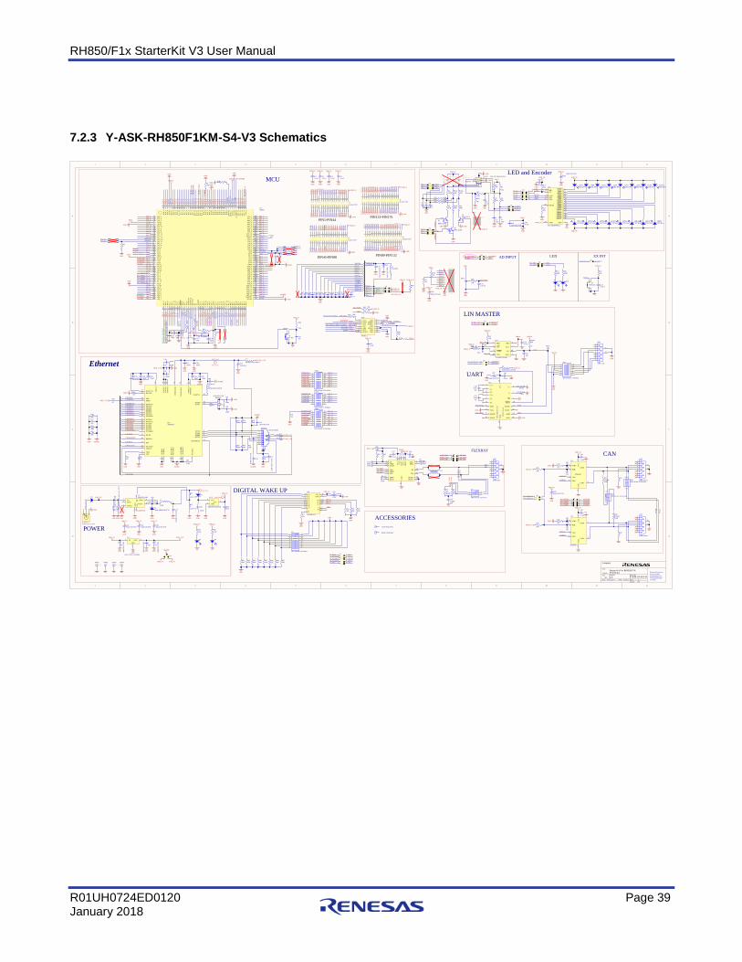
RH850/F1x StarterKit V3 User Manual
R01UH0724ED0120 Page 39 January 2018
7.2.3 Y-ASK-RH850F1KM-S4-V3 Schematics
1
1
2
2
3
3
4
4
5
5
6
6
7
7
8
8
9
9
10
10
11
11
12
12
D D
C C
B B
A A
1
Renesas ElectronicsEurop e GmbHArcadiastrasse 1040472 DüsseldorfGermany107.02.2017 15:05:21
Title
Size Number
Date:
Revision
Sheet ofTime:A1
Starter Kit For RH850/F1X
2.0
HS
Company
Author
Variant F1KM-S4
0R17
P10_
0P1
0_1
P10_
2
P10_3P10_4P10_5
P10_
6P1
0_7
P10_
8P1
0_9
P10_
10P1
0_11
P10_
12P1
0_13
P10_
14
P10_15P11_0
P11_
1P1
1_2
P11_
3P1
1_4
P11_
5P1
1_6
P11_
7
P11_8P11_9P11_10P11_11P11_12
P11_13P11_14
P11_
15P1
2_0
P12_
1P1
2_2
P12_3P12_4P12_5P0_0P0_1P0_2P0_3
P0_4P0_5P0_6
P0_7
P0_8
P0_9
P0_1
0
P0_11P0_12P0_13P0_14
JP0_
6
P1_0P1_1P1_2P1_3
P1_4
P1_5
P1_6
P1_7
P1_8
P1_9
P1_1
0P1
_11
P1_12P1_13
P1_1
4P1
_15
P2_0
P2_1
P2_2
P2_3
P2_4
P2_5
P2_6
P8_0
P8_1
P8_3
P8_2
P8_4
P8_5
P8_6
P8_7
P8_8
P8_9
P8_10P8_11P8_12
JP0_
0JP
0_1
JP0_
2
JP0_3JP0_4JP0_5
IP0_
0
AP0_0AP0_1AP0_2AP0_3AP0_4AP0_5AP0_6AP0_7AP0_8AP0_9AP0_10AP0_11AP0_12AP0_13AP0_14AP0_15
P9_0P9_1P9_2P9_3
P9_4P9_5P9_6
P20_0P20_1P20_2P20_3
P20_4P20_5
AP1
_0
AP1_1AP1_2AP1_3AP1_4AP1_5AP1_6AP1_7AP1_8AP1_9AP1_10AP1_11
AP1
_12
AP1
_13
AP1
_14
AP1
_15
P18_
0P1
8_1
P18_
2P1
8_3
P18_
4P1
8_5
P18_
6P1
8_7
MCU
RESET
FLMD0
DCUTDI_FLCS0SI_FLUR0RXDCUTDO_FLCS0SO_FLUR0TX
DCUTCK_FLCS0SCI
DCUTMS
DCUTRST
DCURDY
DC
UT
DI_
FLC
S0SI
_FL
UR
0RX
DC
UT
DO
_FL
CS0
SO_F
LU
R0T
XD
CU
TC
K_F
LC
S0SC
I
DCUTMS
DCURDYDCUTRST
FLM
D0
RE
SET
5K6
R38
1nFC32S2
SPST-NO
VDD_5V
RESET
100K
R43
BVSS
EVSS
EV
CC
1
AW
0VSS
AW
OV
CL
RE
G0V
CC
EV
SS
A0VSSA0VREF
EVSS
EVCC2A
1VR
EF
A1V
SSB
VC
C1
ISO
VC
L3
IS0V
SS3
BVCC
EVCCEVCC1EVCC2AWOVCLREG0VCCA0VREFA1VREF
BVCC1
ISOVCL0
GND
GND
BV
CC
2B
VSS
GND
BVCC
EVCC
EVCC1 AWOVCL
REG0VCC
GND
A0VREF
A1VREFBVCC1BVCC2
BVCC
EVCC
EVCC2
BV
SS
GND
GNDGND
47KR81
47KR82
47KR83
47KR84
47KR88
47KR86
47KR85
47KR87
DIGITAL WAKE UP
GND
DPO
0.1uF
C27
0.1uF
C26
0.1uF
C20
0.1uF
C24
0.1uF
C23
0.1uF
C22
0.1uF
C21
0.1uF
C25
0.1uF
C19
0.1uF
C18
GND
1 216MHzY2
10pFC34
10pFC33
X1
X2
X1X2
0.1uF
C59
GND
10KR77
GND
DIN
DIN_CDIN_BDIN_AI31 I22 I13 I04
Y 5
Y 6
E7
GND 8
S2 9S1 10S0 11
I712 I613 I514 I415
VCC 16IC8
CD74HC151
10KR76
10KR74
10KR75
GND
XT1 XT2
10pFC30
10pFC31
1 232.768kHzY1
XT
1
100K
R37
0
R36 TCK1 GND 2
TRST3 FPMD0 4
TDO5 FPMD1 6
TDI7 VDD 8
TMS9 RESET 10
RDY11 GND 12
RESET13 GND 14
CN3
Flash E1
TCK_FSCI
TRSTTDO_FTXSOTDI_FSIRXTMSTRDYFLDBG_RESET
FLDBG_FLMD0
GND
GND
VDD_5V
10KR32VDD_5V
10KR1
0.1uF
C17
BVCC2
M_SELDP2M_SELDP1M_SELDP0
M_D
IN0
M_RX0_RS232M_TX0_RS232
M_R
X1_
LIN
M_T
X1_
LIN
M_CANRX0
M_CANTX1M_CANRX1M_CANTX0
M_A
DC
A1I
0
BP1BM1INH2 1INH1 2EN3
VIO
4
TXD5
TXEN6
RXD7
BG
E8
STBN9
TRXD1 10TRXD0 11
RXEN12 ERRN13
VB
AT
14
WAKE15
GN
D16
BM 17
BP 18
VC
C19
VB
UF
20
IC7TJA1080
0.1uF
C56
4700pF50V
C61
0
R68
0
R69
FR_TXD
FR_RXDFR_TXEZ
VDD_5VVBATF
51R250mW
R7051R250mW
R71
L4
0R63
BVCC
TP12
0R62
TP14TP16
123456
J8
FR_TXD
FR_RXDFR_TXEZ
M_FR_TXD
M_FR_RXDM_FR_TXEZ
M_F
R_T
XD
M_F
R_R
XD
M_F
R_T
XE
Z
GND
GND
BVCCBVCC1BVCC2
EVCCEVCC1EVCC2
REG0VCC
A0VREFA1VREF
VDD_5V
FLEXRAY
12345678 9
10111213141516
S3
DIP Switch, 8 Position
VDD_5V
FL_C
ON
1FL
_CO
N2
S_FL
_CO
N1
S_FL
_CO
N2
FLMD1
M_APOM_DPO
M_LED1
M_I
NT
P12
POT1
APO
10KR21
S1SPST-NO
VDD_5V
0.01uFC14
INTP12
390RR19
A1
K2
LED2
390RR20
LED1
AD INPUT LED EX INT
GND
0.01uFC12
ADCA0I0S
LED and Encoder
GND
39RR106
1nFC9
10nFC8
10KR14
100RR6
39RR104
10KR13
1.8KR80
5.6KR79
D3 D4
VDD_5V
POWER
VBATF
VDD_5V
VDD_12V
1 32
J11
VDD_12V VDD_5V
TP13TP15
TP17
TP18
1 23 45 67 89 10
J9 DINDIN_ADIN_BDIN_CM_SELDP2
M_SELDP1M_SELDP0M_DIN0
DPOM_DPO
ADCA0I0SM_ADCA0I0SAPOM_APO
1 23 4
J151 2J16
LED1M_LED1LED2M_LED2
M_INTP12 INTP12
0R39
12
34
56
78
910
1112
1314
1516
1718
1920
2122
2324
2526
2728
2930
3132
3334
3536
3738
3940
J4Jumper 20x2
12
34
56
78
910
111 2
1314
1516
1718
1920
2122
2324
2526
272 8
2930
3132
3334
3536
3738
3940
J2Jumper 20x2
12
34
56
78
910
1112
1314
1516
1718
1920
2122
2324
2526
2728
2930
3132
3 334
3536
3738
3940
J1Jumper 20x2
12
34
56
78
910
1112
1314
1516
1718
1920
2122
2324
2526
2728
2 930
3132
3334
3536
3738
3940
J3Jumper 20x2
GND
VDD_5V
AP0
_0A
P0_ 1
AP0
_2A
P0_3
AP0
_4A
P0_5
AP0
_6A
P0_7
AP0
_8A
P0_9
AP0
_10
AP0
_11
AP0
_12
AP0
_13
AP0
_ 14
AP0
_15
P9_0
P9_1
P9_2
P9_3
P9_4
P9_5
P9_6
P20_
0P2
0_1
P20_
2P2
0_3
P20_
4P2
0_5
AP1
_0A
P1_1
AP1
_2A
P1_3
AP1
_4A
P1_ 5
AP1
_6A
P1_7
AP1
_8
GND
VDD_5V
AP1
_9A
P1_1
0A
P1_1
1A
P1_1
2A
P1_1
3A
P1_1
4A
P1_1
5P1
8_0
P18_
1P1
8_2
P18_
3P1
8_4
P18_
5P1
8_6
P18_
7P1
0_0
P10_
1P1
0_2
P10_
3P1
0_4
P10_
5P1
0_6
P10_
7P1
0_8
P10_
9P1
0_10
P10_
11P1
0_12
P10_
13P1
0_14
P10_
15P1
2_0
P12_
1P1
2_2
P12_
3P1
2_4
P12_
5P1
1_0
GND
VDD_5V
P11_
1P1
1_2
P11_
3P1
1_4
P11_
5P1
1_6
P11_
7P1
1_8
P11_
9P1
1_10
P11_
11P1
1_12
P11_
13P1
1_14
P11_
15P0
_0P0
_1P0
_2P0
_3P0
_4P0
_5P0
_6P0
_7P0
_8P0
_9P0
_10
P0_1
1P0
_12
P0_1
3P0
_14
JP0_
6
JP0_
0JP
0_1
JP0_
2J P
0_3
JP0_
4JP
0_5
P1_1
5
P1_0
P1_1
P1_2
P1_3
P1_4
P1_5
P1_6
P1_7
P1_8
P1_9
P1_1
0P1
_11
P1_1
2P1
_13
P1_1
4
IP0_
0FL
MD
0R
ESE
TP2
_0P2
_1P2
_2P2
_3P2
_4P2
_5P2
_6P8
_0P8
_1P8
_2P 8
_3P8
_4P8
_5P8
_6P8
_7P8
_8P8
_9P8
_10
P8_1
1P8
_12
GND
VDD_5V
M_L
ED
2
M_ADCA0I0S
10K
R24
GND 5
LIN 6
BAT 7
INH 8
TXD4
RXD1
SLP2
WAKE3
IC4
TJA1020/TJA1021
0.1uFC29
LIN1
RX1_LIN
TX1_LIN
VBATF
VDD_5V
VBATF VBATF
VBATF
VDD_5V
10KR42
1nFC35
LIN MASTER1 23 4J17 RX1_LIN
TX1_LINM_RX1_LINM_TX1_LIN
250mW
1K
R44
1KR451KR46
RTX0
RRX0
TX0_RS232
RX0_RS232
47nF16V
C49
0.1uF
C42
VDD_5V
330nF16V
C52
330nF16V
C50
330nF16V
C51
UART
1 23 4J18 TX0_RS232
RX0_RS232M_TX0_RS232M_RX0_RS232
GND
GND
TP9
TP11
123456 7
89101112
S10
DIP Switch, 6 Position
GND
GND
12
43
S7
DIP Switch, 2 Position
M_CANNSIL0
M_CANNSIL1
PIN45-PIN88 PIN89-PIN132
PIN133-PIN176PIN1-PIN44
TP10
TDI_FSIRX
C1+2
C1-4
C2+5
C2-6
V+ 3
V- 7
T1IN13
T2IN12
R1OUT15
R2OUT10 GN
D18
VC
C19
R2IN 9
R1IN 16
T2OUT 8
T1OUT 17
TT
L/C
MO
SL
evel
RS2
32L
evel
EN 1
SHDN 20NC11
NC14
IC5
FLM
D1
GND
0R16
0.1uF
C11
0
R18
TRST 10KR33GND
100RR34
0.1uFC2
0.1uFC3
0.1uFC4
0.1uFC5
GND GND GND GND
VDD_5V VDD_5V VDD_5V VDD_5V
GND4GND3GND2GND1
L174279214
10µF
/10V
/X5R
C15
10nF
/X7R
/50V
C16
GND GND
Ethernet
ETH0MDCETH0MDIO
ETH0RXCLKETH0RXD0ETH0RXD1ETH0RXD2ETH0RXD3
ETH0RXDV
ETH0RXERR
ETH0TXEN
ETH0TXCLK
ETH0TXD0ETH0TXD1ETH0TXD2ETH0TXD3
ETH0TXERR
ETH0CRS
ETH0RESETB
ETH0INT
ETH0COLSD
P10_0P10_1P10_2P10_4P10_5
P11_9P11_10P11_11P11_13P11_14P12_4P12_5
P18_0ETH0LINKP18_1P18_2P18_3P18_4P18_5P18_6P18_7
12345678 9
10111213141516
ETH3
DIP Switch, 8 Position
12345678 9
10111213141516
ETH1
DIP Switch, 8 Position
123456 7
89101112
ETH2
DIP Switch, 6 Position
P11_6
1K
R15
0.1uF
C10
1K
R31
0.1uF
C28
CANTX0
CANRX0
CANTX1
CANRX1
VDD_5V
VDD_5V
CA
NH
CA
NL
250mW120R
R22
250mW120R
R30
TP1
TP5
CAN
CANTX0CANRX0CANTX1CANRX1
M_CANRX0M_CANTX1M_CANRX1
M_CANTX0 1 23 45 67 8
J7
TP3
TP7
3 46 5
S4BDIP Switch, 4 Position
0R23
0R35
1 28 7
S4ADIP Switch, 4 Position1 2
3 4
J6M_CANNSIL0M_CANNSIL1
VDD_5V
VDD_5V
10K
R26
10K
R40
VDD_3.3V
IN3 OUT 4
1
GND
U3
LM1117DT-3.3/NOPB
10nF
/50V
/X7R
C68 C70
10µF
/10V
/X7R
VDD_3.3V
C69
10µF
/10V
/X7R
GNDGND GNDGND
12k4
R67
EX
TR
ES
1
ATP2
P0TXP 3
P0TXN 4
P0A
GN
D1
5
P0RXP 6
P0RXN 7
P0A
GN
D2
8
VD
DA
159
VD
D33
ESD
10
VD
D15
11
P0LINKLED 12
MDC13
MDIO14
INT15
P0RXCLK16
P0RXD317 P0RXD218
VD
DIO
119
GN
DIO
120
P0RXD121 P0RXD022
P0RXDV23
P0RXERR24
P0TXEN25
P0TXD026
P0TXD127
P0TXD228
P0TXD329
P0TXCLK30
VD
DIO
231
XCLK0 32
XCLK1 33
GPIO1434
P0TXERR35
GN
DIO
236
DVOUT1537
VD
DIO
338
P0CRS39
RESETB40
TEST41
P0COLSD42
GN
DA
RE
F43
REGOFF44
AVOUT15 45
VD
DA
33R
EG
46
VD
DA
PLL
47
GN
DA
PLL
48
IC6uPD60610
4k7R65
4k7R47
10pF
C54
10pF
C53
0R0R49
12
25M
Hz
8pF
Digi-Key644-1041-1-ND
Q1
49R9R59
49R9R60
49R9R52
49R9R53
10RR54
10nF/50V/X7RC55
100nF
C41
100nFC36
100nFC40
100nFC45
100nFC44
L3BLM21AG121SN1D
22µF/35V
C48100nFC47
100nFC46
L2
BLM21AG121SN1D
22µF/35VC39
100nFC38
100nFC37
10µF/6.3V/X7RC43
4k7
R48
0R0
R50
0R0
R51
0R0
R55
0R0
R56
10RR61
10nF
/50V
/X7R
C58
220RR57
220RR58
8765
MH
2M
H1
23
1
49101211
J0011D21BNLEthernet
2MR66
2.2n
F/10
00V
/X7R
C574k7R64
GND AGNDEGND
GND
GND
GND
AGNDE
VDD_3.3V GND
GND
AGNDE
AGNDE
GND
VDD_3.3V
GNDGND
VDD_3.3V
AGNDE
VCC3.3_F
ETH0LINK
GND
VDD_3.3V
iNet Class
VDD_3.3V
GND
ETH0MDCETH0MDIO
ETH0RXCLKETH0RXD0ETH0RXD1ETH0RXD2ETH0RXD3ETH0RXDVETH0RXERR
ETH0TXENETH0TXCLKETH0TXD0ETH0TXD1ETH0TXD2ETH0TXD3ETH0TXERR
ETH0CRS
ETH0RESETB
ETH0INT
ETH0COLSD
GND AGNDE
GNDGND
naC67
GND
10nF/50V/X7R
C60 5K23 1%
R72
1K64 1%
R73
GND
GND3 OUT 2VCC1FC1
NFE31PT222Z1E9L
100nF
C62
GNDGND GND
100nFC63
VDD_5V
i Net Class
iNet Class
3,3µ
F/50
VK
eram
ikz.
B.A
VX
C65
GND
Cboot 1
SoftStart2
SYNC3 FB4
ON
5G
ND
6
Vin7
Vswitch 8
U2LM22670-ADJ
D2Diode MBRS240LT3G
10µH
L5
WAKEPWRGND
9-15V (+)-Powe rCon 2.1mm
D1
VD
D_1
2V_I
N
VDD_12V
0R28
0R29
100µ
F/16
V/X
5R
C72
GND
100µ
F/16
V/X
5RC
71
GND
F1KM-S4-003-01
0.1uF
C73
1
2
3
4
5
6
7
8
9
11
10
CN4
DB9 male
1
2
3
4
5
6
7
8
9
11
10
CN5
DB9 male
1
2
3
4
5
6
7
8
9
11
10
CN1
DB9 female
1
2
3
4
5
6
7
8
9
11
10
CN2
DB9 female
10kR78
GND
0R0
R89
ACCESSORIESJumperBag 34pc.
Rubber Pads 4pc.
TXD1
GN
D2
RXD4
NSIL5
VC
C3
CANL 6
CANH 7STBY8
IC1
ATA6560
TXD1
GN
D2
RXD4
NSIL5
VC
C3
CANL 6
CANH 7STBY8
IC3
ATA6560
GND
GND
0.1uF
C74
0.1uF
C75
0R900R91
0R93
GND
ISOVCL0IS0VSS0
ISOVCL2IS0VSS2
0
R92
0R94
ISO
VC
L1
IS0V
SS1
0R95
ISOVCL3ISOVCL2
4 2 1
bca
35
ENC1 PEL12T-4225S-S1024
GND 1
SDI2 CLK3
LE4 OUT0 5
OUT1 6
OUT2 7
OUT3 8
OUT4 9
OUT5 10
OUT6 11
OUT7 12
OUT8 13
OUT9 14
OUT10 15
OUT11 16
OUT12 17
OUT13 18
OUT14 19
OUT15 20
OE21
SDO22
R-EXT23
VDD24
IC2
TLC5925IPWRG4
LED3LED Blue
LED4LED Blue
LED5LED Blue
LED6LED Blue
LED7LED Blue
LED8LED Blue
LED9LED Blue
LED10LED Blue
LED18LED Blue
LED17LED Blue
LED16LED Blue
LED15LED Blue
LED14LED Blue
LED13LED Blue
LED12LED Blue
LED11LED Blue
VDD_5V
VDD_5V
VDD_5V
GND
MOSIMISO
MCLK
LAT
VDD_5V
BLNK1 23 45 67 89 10
J12
P0_12P0_13P0_14
P1_14P1_15
Q3
PDTC123JT
Q4PDTC123JT
Q2PDTC123JT
1 23 45 6
J13
123456
J19
1 23 45 6
J20
AP0_3AP0_1
AP0_2
P1_4
P10_9P10_10
P20_2
P20_0P20_1
VDD_5V
GND
GNDGND
GND
VDD_5V GND
10K
R100
10K
R5
GND GND
10nFC1
10K
R310KR2
GND GND
10KR7
10KR8
BVCC
PWM
.R
PWM.G
PWM
.B
FB.RFB.GFB.B
a2
b4
b3
a1
BUT
VDD_5V
1234567891011
OLED
Header 11
VDD_5V
GND
P11_2P11_3P11_0P10_12P11_15P12_1P11_4P11_5AP0_4
10KR11
GND
RED
GR
EEN
BLU
E CLED1RGB LED
1nF
C6
10KR25
1nF
C7
10KR10
1nF
C13
10KR12
GND
0R101
0R102
GND
0.1uF
C79
ISOVCL1
0.1uF
C80
GND
1µF 16V X7RC81
0.1uFC82
GND
BVCC
0.1uFC83
GND
VDD_5V
47KR103
BVCC
1 23 4
J14
47RR9
47RR4
47RR105
P10_31
P10_42
P10_53
BVCC4
BVSS5
P10_156
P11_07
P11_88
P11_99
P11_1010
P11_1111
P11_1212
P11_1313
P11_1414
P12_315
P12_416
P12_517
P0_018
P0_119
P0_220
P0_321
EVCC22
P0_423
P0_524
P0_625
P0_1126
P0_1227
P0_1328
P0_1429
P1_030
P1_131
P1_232
P1_333
P1_1234
P1_1335
P2_636
EVSS37
P8_238
P8_1039
P8_1140
P8_1241
JP0_542
JP0_443
JP0_344
JP0_
245
JP0_
146
JP0_
047
P2_1
48
P2_0
49
P1_1
150
P1_1
051
P1_9
52
P1_8
53
RE
SET
54
EV
CC
55
XT
156
IP0_
057
AW
OV
SS58
AW
OV
CL
59
RE
GV
CC
60
X2
61
X1
62
FLM
D0
63
P2_3
64
P2_2
65
JP0_
666
P0_1
067
P0_9
68
P0_8
69
P0_7
70
EV
SS71
P1_7
72
P1_6
73
P1_5
74
P1_4
75
P2_4
76
P2_5
77
P1_1
478
P1_1
579
P8_0
80
P8_1
81
P8_3
82
P8_4
83
P8_5
84
P8_6
85
P8_7
86
P8_8
87
P8_9
88
A0VSS 89A0VREF 90AP0_15 91AP0_14 92AP0_13 93AP0_12 94AP0_11 95AP0_10 96AP0_9 97AP0_8 98AP0_7 99AP0_6 100AP0_5 101AP0_4 102AP0_3 103AP0_2 104AP0_1 105AP0_0 106EVSS 107P9_0 108P9_1 109P9_2 110P9_3 111P9_4 112P9_5 113P9_6 114P20_3 115P20_2 116P20_1 117P20_0 118P20_5 119P20_4 120EVCC 121AP1_11 122AP1_10 123AP1_9 124AP1_8 125AP1_7 126AP1_6 127AP1_5 128AP1_4 129AP1_3 130AP1_2 131AP1_1 132
AP1
_013
3A
P1_1
513
4A
P1_1
413
5A
P1_1
313
6A
P1_1
213
7A
1VR
EV
F13
8A
1VSS
139
BV
CC
140
ISO
VC
L14
1IS
OV
SS14
2P1
8_0
143
P18_
114
4P1
8_2
145
P18_
314
6P1
8_4
147
P18_
514
8P1
8_6
149
P18_
715
0B
VSS
151
P10_
615
2P1
0_7
153
P10_
815
4P1
0_9
155
P10_
1015
6P1
0_11
157
P10_
1215
8P1
0_13
159
P10_
1416
0P1
1_1
161
P11_
216
2P1
1_3
163
P11_
416
4P1
1_5
165
P11_
616
6P1
1_7
167
P11_
1516
8P1
2_0
169
P12_
117
0P1
2_2
171
BV
CC
172
BV
SS17
3P1
0_0
174
P10_
117
5P1
0_2
176
U1RH850
C87
10µF/10V/X7RGND
C8810µF/10V/X7R
GND
VDD_5V
C8610µF/10V/X7R
GND
VDD_5V
C6410µF/10V/X7R
GND
VDD_5V
C6610µF/10V/X7R
GND
VDD_5V
C8410µF/10V/X7R
GND
VDD_5V
C8510µF/10V/X7R
GND
VDD_5V
0R107
10KR96
JP0_6
0.1uF
C890R108
IS0VSS2
ISOx
0R410R27
REG0VCCREG1VCC
1 23 45 6
J5
VDD_5V
VDD_5V VDD_3.3V
EVCCBVCC
REG1VCC
D5
L6
BLM21AG121SN1D
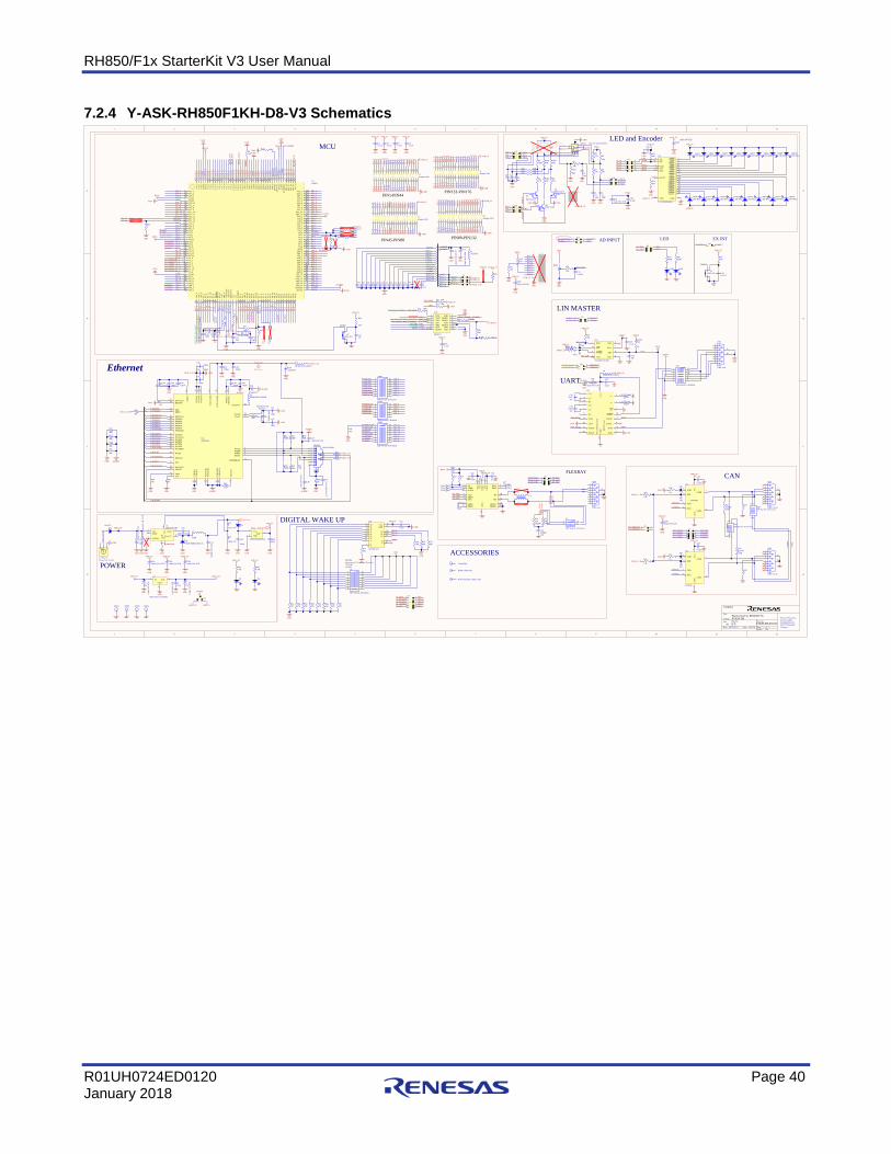
RH850/F1x StarterKit V3 User Manual
R01UH0724ED0120 Page 40 January 2018
7.2.4 Y-ASK-RH850F1KH-D8-V3 Schematics
1
1
2
2
3
3
4
4
5
5
6
6
7
7
8
8
9
9
10
10
11
11
12
12
D D
C C
B B
A A
1
Renesas ElectronicsEurop e GmbHArcadiastrasse 1040472 DüsseldorfGermany106.09.2017 10:43:50
Title
Size Number
Date:
Revision
Sheet ofTime:A1
Starter Kit For RH850/F1X
3.0
HS
Company
Author
Variant F1KM-D8
0R17
P10_
0P1
0_1
P10_
2
P10_3P10_4P10_5
P10_
6P1
0_7
P10_
8P1
0_9
P10_
10P1
0_11
P10_
12P1
0_13
P10_
14
P10_15P11_0
P11_
1P1
1_2
P11_
3P1
1_4
P11_
5P1
1_6
P11_
7
P11_8P11_9P11_10P11_11P11_12
P11_13P11_14
P11_
15P1
2_0
P12_
1P1
2_2
P12_3P12_4P12_5P0_0P0_1P0_2P0_3
P0_4P0_5P0_6
P0_7
P0_8
P0_9
P0_1
0P0_11P0_12P0_13P0_14
JP0_
6
P1_0P1_1P1_2P1_3
P1_4
P1_5
P1_6
P1_7
P1_8
P1_9
P1_1
0P1
_11
P1_12P1_13
P1_1
4P1
_15
P2_0
P2_1
P2_2
P2_3
P2_4
P2_5
P2_6
P8_0
P8_1
P8_3
P8_2
P8_4
P8_5
P8_6
P8_7
P8_8
P8_9
P8_10P8_11P8_12
JP0_
0JP
0_1
JP0_
2
JP0_3JP0_4JP0_5
IP0_
0
AP0_0AP0_1AP0_2AP0_3AP0_4AP0_5AP0_6AP0_7AP0_8AP0_9AP0_10AP0_11AP0_12AP0_13AP0_14AP0_15
P9_0P9_1P9_2P9_3
P9_4P9_5P9_6
P20_0P20_1P20_2P20_3
P20_4P20_5
AP1
_0
AP1_1AP1_2AP1_3AP1_4AP1_5AP1_6AP1_7AP1_8AP1_9AP1_10AP1_11
AP1
_12
AP1
_13
AP1
_14
AP1
_15
P18_
0P1
8_1
P18_
2P1
8_3
P18_
4P1
8_5
P18_
6P1
8_7
MCU
RESET
FLMD0
DCUTDI_FLCS0SI_FLUR0RXDCUTDO_FLCS0SO_FLUR0TX
DCUTCK_FLCS0SCI
DCUTMS
DCUTRST
DCURDY
DC
UT
DI_
FLC
S0SI
_FL
UR
0RX
DC
UT
DO
_FL
CS0
SO_F
LU
R0T
XD
CU
TC
K_F
LC
S0SC
I
DCUTMS
DCURDYDCUTRST
FLM
D0
RE
SET
5K6
R38
1nFC32S2
SPST-NO
VDD_5V
RESET
100K
R43
BVSS
EVSS
EV
CC
1
AW
0VSS
AW
OV
CL
RE
G0V
CC
EV
SS
A0VSSA0VREF
EVSS
EVCC2
A1V
RE
FA
1VSS
BV
CC
1IS
OV
CL
3IS
0VSS
3
BVCC
EVCCEVCC1EVCC2AWOVCLREG0VCCA0VREFA1VREF
BVCC1
ISOVCL0
GND
GNDB
VC
C2
BV
SS
GND
BVCC
EVCC
EVCC1 AWOVCL
REG0VCC
GND
A0VREF
A1VREFBVCC1BVCC2
BVCC
EVCC
EVCC2
BV
SS
GND
GNDGND
47KR81
47KR82
47KR83
47KR84
47KR88
47KR86
47KR85
47KR87
DIGITAL WAKE UP
GND
DPO
0.1uF
C27
0.1uF
C26
0.1uF
C20
0.1uF
C24
0.1uF
C23
0.1uF
C22
0.1uF
C21
0.1uF
C25
0.1uF
C19
0.1uF
C18
GND
1 216MHzY2
10pFC34
10pFC33
X1
X2
X1X2
0.1uF
C59
GND
10KR77
GND
DIN
DIN_CDIN_BDIN_AI31 I22 I13 I04
Y 5
Y 6
E7
GND 8
S2 9S1 10S0 11
I712 I613 I514 I415
VCC 16IC8
CD74HC151
10KR76
10KR74
10KR75
GND
XT1 XT2
10pFC30
10pFC31
1 232.768kHzY1
XT
1
100K
R37
0
R36 TCK1 GND 2
TRST3 FPMD0 4
TDO5 FPMD1 6
TDI7 VDD 8
TMS9 RESET 10
RDY11 GND 12
RESET13 GND 14
CN3
Flash E1
TCK_FSCI
TRSTTDO_FTXSOTDI_FSIRXTMSTRDYFLDBG_RESET
FLDBG_FLMD0
GND
GND
VDD_5V
10KR32VDD_5V
10KR1
0.1uF
C17
BVCC2
M_SELDP2M_SELDP1M_SELDP0
M_D
IN0
M_RX0_RS232M_TX0_RS232
M_R
X1_
LIN
M_T
X1_
LIN
M_CANRX0
M_CANTX1M_CANRX1M_CANTX0
M_A
DC
A1I
0
BP1BM1INH2 1INH1 2EN3
VIO
4
TXD5
TXEN6
RXD7
BG
E8
STBN9
TRXD1 10TRXD0 11
RXEN12 ERRN13
VB
AT
14
WAKE15
GN
D16
BM 17
BP 18
VC
C19
VB
UF
20IC7TJA1080
0.1uF
C56
4700pF50V
C61
0
R68
0
R69
FR_TXD
FR_RXDFR_TXEZ
VDD_5VVBATF
51R250mW
R7051R250mW
R71
L4
0R63
BVCC
TP12
0R62
TP14TP16
123456
J8
FR_TXD
FR_RXDFR_TXEZ
M_FR_TXD
M_FR_RXDM_FR_TXEZ
M_F
R_T
XD
M_F
R_R
XD
M_F
R_T
XE
Z
GND
GND
BVCCBVCC1BVCC2
EVCCEVCC1EVCC2
REG0VCC
A0VREFA1VREF
VDD_5V
FLEXRAY
12345678 9
10111213141516
1123955718-2190Anony mous D aily Limit Reached9472096
S3
DIP Switch, 8 Position
VDD_5V
FL_C
ON
1FL
_CO
N2
S_FL
_CO
N1
S_FL
_CO
N2
FLMD1
M_APOM_DPO
M_LED1M
_IN
TP1
2
POT1
APO
10KR21
S1SPST-NO
VDD_5V
0.01uFC14
INTP12
390RR19
A1
K2
LED2
390RR20
LED1
AD INPUT LED EX INT
GND
0.01uFC12
ADCA0I0S
LED and Encoder
GND
39RR106
1nFC9
10nFC8
10KR14
100RR6
39RR104
10KR13
1.8KR80
5.6KR79
D3 D4
VDD_5V
POWER
VBATF
VDD_5V
VDD_12V
1 32
J11
VDD_12V VDD_5V
TP13TP15
TP17
TP18
1 23 45 67 89 10
J9 DINDIN_ADIN_BDIN_CM_SELDP2
M_SELDP1M_SELDP0M_DIN0
DPOM_DPO
ADCA0I0SM_ADCA0I0SAPOM_APO
1 23 4
J151 2J16
LED1M_LED1LED2M_LED2
M_INTP12 INTP12
0R39
12
34
56
78
910
1112
1314
1516
1718
1920
2122
2324
2526
2728
2930
3132
3334
3536
3738
3940
J4Jumper 20x2
12
34
56
78
910
111 2
1314
1516
1718
1920
2122
2324
2526
272 8
2930
3132
3334
3536
3738
3940
J2Jumper 20x2
12
34
56
78
910
1112
1314
1516
1718
1920
2122
2324
2526
2728
2930
3132
3 334
3536
3738
3940
J1Jumper 20x2
12
34
56
78
910
1112
1314
1516
1718
1920
2122
2324
2526
2728
2 930
3132
3334
3536
3738
3940
J3Jumper 20x2
GND
VDD_5V
AP0
_0A
P0_ 1
AP0
_2A
P0_3
AP0
_4A
P0_5
AP0
_6A
P0_7
AP0
_8A
P0_9
AP0
_10
AP0
_11
AP0
_12
AP0
_13
AP0
_ 14
AP0
_15
P9_0
P9_1
P9_2
P9_3
P9_4
P9_5
P9_6
P20_
0P2
0_1
P20_
2P2
0_3
P20_
4P2
0_5
AP1
_0A
P1_1
AP1
_2A
P1_3
AP1
_4A
P1_ 5
AP1
_6A
P1_7
AP1
_8
GND
VDD_5V
AP1
_9A
P1_1
0A
P1_1
1A
P1_1
2A
P1_1
3A
P1_1
4A
P1_1
5P1
8_0
P18_
1P1
8_2
P18_
3P1
8_4
P18_
5P1
8_6
P18_
7P1
0_0
P10_
1P1
0_2
P10_
3P1
0_4
P10_
5P1
0_6
P10_
7P1
0_8
P10_
9P1
0_10
P10_
11P1
0_12
P10_
13P1
0_14
P10_
15P1
2_0
P12_
1P1
2_2
P12_
3P1
2_4
P12_
5P1
1_0
GND
VDD_5V
P11_
1P1
1_2
P11_
3P1
1_4
P11_
5P1
1_6
P11_
7P1
1_8
P11_
9P1
1_10
P11_
11P1
1_12
P11_
13P1
1_14
P11_
15P0
_0P0
_1P0
_2P0
_3P0
_4P0
_5P0
_6P0
_7P0
_8P0
_9P0
_10
P0_1
1P0
_12
P0_1
3P0
_14
JP0_
6
JP0_
0JP
0_1
JP0_
2J P
0_3
JP0_
4JP
0_5
P1_1
5
P1_0
P1_1
P1_2
P1_3
P1_4
P1_5
P1_6
P1_7
P1_8
P1_9
P1_1
0P1
_11
P1_1
2P1
_13
P1_1
4
IP0_
0FL
MD
0R
ESE
TP2
_0P2
_1P2
_2P2
_3P2
_4P2
_5P2
_6P8
_0P8
_1P8
_2P 8
_3P8
_4P8
_5P8
_6P8
_7P8
_8P8
_9P8
_10
P8_1
1P8
_12
GND
VDD_5V
M_L
ED
2
M_ADCA0I0S
10K
R24
GND 5
LIN 6
BAT 7
INH 8
TXD4
RXD1
SLP2
WAKE3
IC4
TJA1020/TJA1021
0.1uFC29
LIN1
RX1_LIN
TX1_LIN
VBATF
VDD_5V
VBATF VBATF
VBATF
VDD_5V
10KR42
1nFC35
LIN MASTER1 23 4J17 RX1_LIN
TX1_LINM_RX1_LINM_TX1_LIN
250mW
1K
R44
1KR451KR46
RTX0
RRX0
TX0_RS232
RX0_RS232
47nF16V
C49
0.1uF
C42
VDD_5V
330nF16V
C52
330nF16V
C50
330nF16V
C51
UART
1 23 4J18 TX0_RS232
RX0_RS232M_TX0_RS232M_RX0_RS232
GND
GND
TP9
TP11
123456 7
89101112
S10
DIP Switch, 6 Position
GND
GND
12
43
S7
DIP Switch, 2 Position
M_CANNSIL0
M_CANNSIL1
PIN45-PIN88 PIN89-PIN132
PIN133-PIN176PIN1-PIN44
TP10
TDI_FSIRX
C1+2
C1-4
C2+5
C2-6
V+ 3
V- 7
T1IN13
T2IN12
R1OUT15
R2OUT10 GN
D18
VC
C19
R2IN 9
R1IN 16
T2OUT 8
T1OUT 17
TT
L/C
MO
SL
evel
RS2
32L
evel
EN 1
SHDN 20NC11
NC14
MAX3222 EAP+ -ND732-9216
IC5
FLM
D1
GND
0R16
0.1uF
C11
0
R18
TRST 10KR33GND
100RR34
0.1uFC2
0.1uFC3
0.1uFC4
0.1uFC5
GND GND GND GND
VDD_5V VDD_5V VDD_5V VDD_5V
GND4GND3GND2GND1
L174279214
10µF
/10V
/X5R
C15
10nF
/X7R
/50V
C16
GND GND
Ethernet
ETH0MDCETH0MDIO
ETH0RXCLKETH0RXD0ETH0RXD1ETH0RXD2ETH0RXD3
ETH0RXDV
ETH0RXERR
ETH0TXEN
ETH0TXCLK
ETH0TXD0ETH0TXD1ETH0TXD2ETH0TXD3
ETH0TXERR
ETH0CRS
ETH0RESETB
ETH0INT
ETH0COLSD
P10_0P10_1P10_2P10_4P10_5
P11_9P11_10P11_11P11_13P11_14P12_4P12_5
P18_0ETH0LINKP18_1P18_2P18_3P18_4P18_5P18_6P18_7
12345678 9
10111213141516
ETH3
DIP Switch, 8 Position
12345678 9
10111213141516
ETH1
DIP Switch, 8 Position
123456 7
89101112
ETH2
DIP Switch, 6 Position
P11_6
1K
R15
0.1uF
C10
1K
R31
0.1uF
C28
CANTX0
CANRX0
CANTX1
CANRX1
VDD_5V
VDD_5V
CA
NH
CA
NL
250mW120R
R22
250mW120R
R30
TP1
TP5
CAN
CANTX0CANRX0CANTX1CANRX1
M_CANRX0M_CANTX1M_CANRX1
M_CANTX0 1 23 45 67 8
J7
TP3
TP7
3 46 5
S4BDIP Switch, 4 Position
0R23
0R35
1 28 7
S4ADIP Switch, 4 Position1 2
3 4
J6M_CANNSIL0M_CANNSIL1
VDD_5V
VDD_5V
10K
R26
10K
R40
VDD_3.3V
IN3 OUT 4
1
GND
U3
LM1117DT-3.3/NOPB
10nF
/50V
/X7R
C68 C70
10µF
/10V
/X7R
VDD_3.3V
C69
10µF
/10V
/X7R
GNDGND GNDGND
12k4
R67
EX
TR
ES
1
ATP2
P0TXP 3
P0TXN 4
P0A
GN
D1
5
P0RXP 6
P0RXN 7
P0A
GN
D2
8
VD
DA
159
VD
D33
ESD
10
VD
D15
11
P0LINKLED 12
MDC13
MDIO14
INT15
P0RXCLK16
P0RXD317 P0RXD218
VD
DIO
119
GN
DIO
120
P0RXD121 P0RXD022
P0RXDV23
P0RXERR24
P0TXEN25
P0TXD026
P0TXD127
P0TXD228
P0TXD329
P0TXCLK30
VD
DIO
231
XCLK0 32
XCLK1 33
GPIO1434
P0TXERR35
GN
DIO
236
DVOUT1537
VD
DIO
338
P0CRS39
RESETB40
TEST41
P0COLSD42
GN
DA
RE
F43
REGOFF44
AVOUT15 45
VD
DA
33R
EG
46
VD
DA
PLL
47
GN
DA
PLL
48
IC6uPD60610
4k7R65
4k7R47
10pF
C54
10pF
C53
0R0R49
12
25M
Hz
8pF
Digi-Key644-1041-1-ND
Q1
49R9R59
49R9R60
49R9R52
49R9R53
10RR54
10nF/50V/X7RC55
100nF
C41
100nFC36
100nFC40
100nFC45
100nFC44
L3BLM21AG121SN1D
22µF/35V
C48100nFC47
100nFC46
L2
BLM21AG121SN1D
22µF/35VC39
100nFC38
100nFC37
10µF/6.3V/X7RC43
4k7
R48
0R0
R50
0R0
R51
0R0
R55
0R0
R56
10RR61
10nF
/50V
/X7R
C58
220RR57
220RR58
8765
MH
2M
H1
23
1
49101211
J0011D21BNLEthernet
2MR66
2.2n
F/10
00V
/X7R
C574k7R64
GND AGNDEGND
GND
GND
GND
AGNDE
VDD_3.3V GND
GND
AGNDE
AGNDE
GND
VDD_3.3V
GNDGND
VDD_3.3V
AGNDE
VCC3.3_F
ETH0LINK
GND
VDD_3.3V
iNet Class
VDD_3.3V
GND
ETH0MDCETH0MDIO
ETH0RXCLKETH0RXD0ETH0RXD1ETH0RXD2ETH0RXD3ETH0RXDVETH0RXERR
ETH0TXENETH0TXCLKETH0TXD0ETH0TXD1ETH0TXD2ETH0TXD3ETH0TXERR
ETH0CRS
ETH0RESETB
ETH0INT
ETH0COLSD
GND AGNDE
GNDGND
naC67
GND
10nF/50V/X7R
C60 5K23 1%
R72
1K64 1%
R73
GND
GND3 OUT 2VCC1FC1
NFE31PT222Z1E9L
100nF
C62
GNDGND GND
100nFC63
VDD_5V
i Net Class
iNet Class
3,3µ
F/50
VK
eram
ikz.
B.A
VX
C65
GND
Cboot 1
SoftStart2
SYNC3 FB4
ON
5G
ND
6
Vin7
Vswitch 8
U2LM22670-ADJ
D2Diode MBRS240LT3G
10µH
L5
WAKEPWRGND
9-15V (+)-Powe rCon 2.1mm
1017873D1
VD
D_1
2V_I
N
VDD_12V
0R28
0R29
100µ
F/16
V/X
5R
C72
GND
100µ
F/16
V/X
5RC
71
GND
F1KH-D8-003-03
0.1uF
C73
1
2
3
4
5
6
7
8
9
11
10
CN4
DB9 male
1
2
3
4
5
6
7
8
9
11
10
CN5
DB9 male
1
2
3
4
5
6
7
8
9
11
10
CN1
DB9 female
1
2
3
4
5
6
7
8
9
11
10
CN2
DB9 female
10kR78
GND
0R0
R89
ACCESSORIESJumperBag
Rubber Pads 4pc.
TXD1
GN
D2
RXD4
NSIL5
VC
C3
CANL 6
CANH 7STBY8
IC1
ATA6560
TXD1
GN
D2
RXD4
NSIL5
VC
C3
CANL 6
CANH 7STBY8
IC3
ATA6560
GND
GND
0.1uF
C74
0.1uF
C75
0R900R91
0R93
GND
ISOVCL0IS0VSS0
ISOVCL2IS0VSS2
0
R92
0R94
ISO
VC
L1
IS0V
SS1
0R95
ISOVCL3ISOVCL2
4 2 1
bca
35
ENC1 PEL12T-4225S-S1024
GND 1
SDI2 CLK3
LE4 OUT0 5
OUT1 6
OUT2 7
OUT3 8
OUT4 9
OUT5 10
OUT6 11
OUT7 12
OUT8 13
OUT9 14
OUT10 15
OUT11 16
OUT12 17
OUT13 18
OUT14 19
OUT15 20
OE21
SDO22
R-EXT23
VDD24
IC2
TLC5925IPWRG4
LED3LED Blue
LED4LED Blue
LED5LED Blue
LED6LED Blue
LED7LED Blue
LED8LED Blue
LED9LED Blue
LED10LED Blue
LED18LED Blue
LED17LED Blue
LED16LED Blue
LED15LED Blue
LED14LED Blue
LED13LED Blue
LED12LED Blue
LED11LED Blue
VDD_5V
VDD_5V
VDD_5V
GND
MOSIMISO
MCLK
LAT
VDD_5V
BLNK1 23 45 67 89 10
J12
P0_12P0_13P0_14
P1_14P1_15
Q3
PDTC123JT
Q4PDTC123JT
Q2PDTC123JT
1 23 45 6
J13
123456
J19
1 23 45 6
J20
AP0_3AP0_1
AP0_2
P1_4
P10_9P10_10
P20_2
P20_0P20_1
VDD_5V
GND
GNDGND
GND
VDD_5V GND
10K
R100
10K
R5
GND GND
10nFC1
10K
R310KR2
GND GND
10KR7
10KR8
BVCC
PWM
.R
PWM.G
PWM
.B
FB.RFB.GFB.B
a2
b4
b3
a1
BUT
VDD_5V
1234567891011
OLED
Header 11
VDD_5V
GND
P11_2P11_3P11_0P10_12P11_15P12_1P11_4P11_5AP0_4
10KR11
GND
RED
GR
EEN
BLU
E CLED1RGB LED
1nF
C6
10KR25
1nF
C7
10KR10
1nF
C13
10KR12
GND
0R101
0R102
GND
0.1uF
C79
ISOVCL1
0.1uF
C80
GND
1µF 16V X7RC81
0.1uFC82
GND
BVCC
0.1uFC83
GND
VDD_5V
47KR103
BVCC
1 23 4
J14
47RR9
47RR4
47RR105
P10_31
P10_42
P10_53
BVCC4
BVSS5
P10_156
P11_07
P11_88
P11_99
P11_1010
P11_1111
P11_1212
P11_1313
P11_1414
P12_315
P12_416
P12_517
P0_018
P0_119
P0_220
P0_321
EVCC22
P0_423
P0_524
P0_625
P0_1126
P0_1227
P0_1328
P0_1429
P1_030
P1_131
P1_232
P1_333
P1_1234
P1_1335
P2_636
EVSS37
P8_238
P8_1039
P8_1140
P8_1241
JP0_542
JP0_443
JP0_344
JP0_
245
JP0_
146
JP0_
047
P2_1
48
P2_0
49
P1_1
150
P1_1
051
P1_9
52
P1_8
53
RE
SET
54
EV
CC
55
XT
156
IP0_
057
AW
OV
SS58
AW
OV
CL
59
RE
GV
CC
60
X2
61
X1
62
FLM
D0
63
P2_3
64
P2_2
65
JP0_
666
P0_1
067
P0_9
68
P0_8
69
P0_7
70
EV
SS71
P1_7
72
P1_6
73
P1_5
74
P1_4
75
P2_4
76
P2_5
77
P1_1
478
P1_1
579
P8_0
80
P8_1
81
P8_3
82
P8_4
83
P8_5
84
P8_6
85
P8_7
86
P8_8
87
P8_9
88
A0VSS 89A0VREF 90AP0_15 91AP0_14 92AP0_13 93AP0_12 94AP0_11 95AP0_10 96AP0_9 97AP0_8 98AP0_7 99AP0_6 100AP0_5 101AP0_4 102AP0_3 103AP0_2 104AP0_1 105AP0_0 106EVSS 107P9_0 108P9_1 109P9_2 110P9_3 111P9_4 112P9_5 113P9_6 114P20_3 115P20_2 116P20_1 117P20_0 118P20_5 119P20_4 120EVCC 121AP1_11 122AP1_10 123AP1_9 124AP1_8 125AP1_7 126AP1_6 127AP1_5 128AP1_4 129AP1_3 130AP1_2 131AP1_1 132
AP1
_013
3A
P1_1
513
4A
P1_1
413
5A
P1_1
313
6A
P1_1
213
7A
1VR
EV
F13
8A
1VSS
139
BV
CC
140
ISO
VC
L14
1IS
OV
SS14
2P1
8_0
143
P18_
114
4P1
8_2
145
P18_
314
6P1
8_4
147
P18_
514
8P1
8_6
149
P18_
715
0B
VSS
151
P10_
615
2P1
0_7
153
P10_
815
4P1
0_9
155
P10_
1015
6P1
0_11
157
P10_
1215
8P1
0_13
159
P10_
1416
0P1
1_1
161
P11_
216
2P1
1_3
163
P11_
416
4P1
1_5
165
P11_
616
6P1
1_7
167
P11_
1516
8P1
2_0
169
P12_
117
0P1
2_2
171
BV
CC
172
BV
SS17
3P1
0_0
174
P10_
117
5P1
0_2
176
U1RH850
C87
10µF/10V/X7RGND
C8810µF/10V/X7R
GND
VDD_5V
C8610µF/10V/X7R
GND
VDD_5V
C6410µF/10V/X7R
GND
VDD_5V
C6610µF/10V/X7R
GND
VDD_5V
C8410µF/10V/X7R
GND
VDD_5V
C8510µF/10V/X7R
GND
VDD_5V
0R107
10KR96
JP0_6
0.1uF
C890R108
IS0VSS2
ISOx
0R410R27
REG0VCCREG1VCC
1 23 45 67 8
J5
VDD_5V
VDD_5V VDD_3.3V
EVCCBVCC
REG1VCC
D5
L6
BLM21AG121SN1D
PCB with blue solder resist
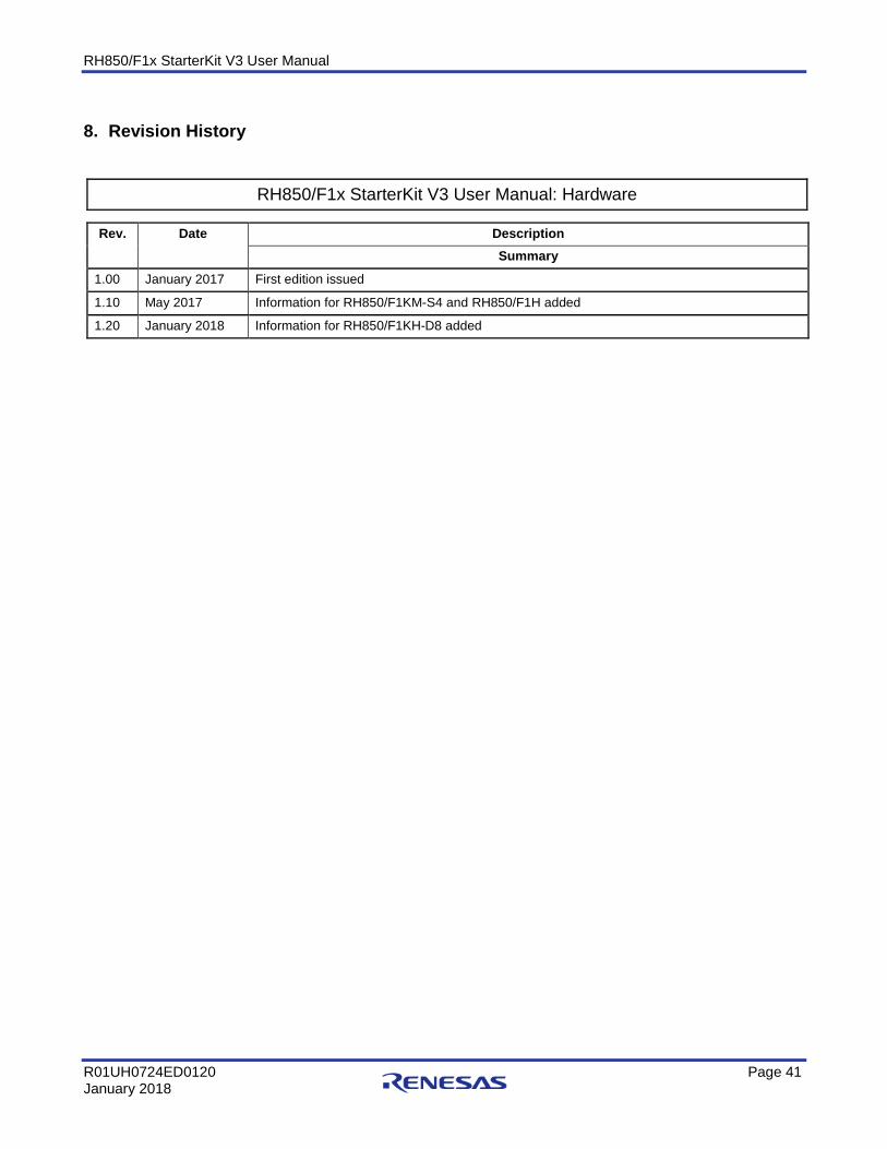
RH850/F1x StarterKit V3 User Manual
R01UH0724ED0120 Page 41 January 2018
8. Revision History
RH850/F1x StarterKit V3 User Manual: Hardware
Rev. Date Description Summary
1.00 January 2017 First edition issued
1.10 May 2017 Information for RH850/F1KM-S4 and RH850/F1H added
1.20 January 2018 Information for RH850/F1KH-D8 added

RH850/F1x StarterKit V3 User Manual: Hardware Publication Date: Rev. 1.20 January 2018 Published by: Renesas Electronics Europe

SALES OFFICES http://www.renesas.com Refer to "http://www.renesas.com/" for the latest and detailed information. Renesas Electronics America Inc. 2880 Scott Boulevard Santa Clara, CA 95050-2554, U.S.A. Tel: +1-408-588-6000, Fax: +1-408-588-6130 Renesas Electronics Canada Limited 1101 Nicholson Road, Newmarket, Ontario L3Y 9C3, Canada Tel: +1-905-898-5441, Fax: +1-905-898-3220 Renesas Electronics Europe Limited Dukes Meadow, Millboard Road, Bourne End, Buckinghamshire, SL8 5FH, U.K Tel: +44-1628-585-100, Fax: +44-1628-585-900 Renesas Electronics Europe GmbH Arcadiastrasse 10, 40472 Düsseldorf, Germany Tel: +49-211-65030, Fax: +49-211-6503-1327 Renesas Electronics (China) Co., Ltd. 7th Floor, Quantum Plaza, No.27 ZhiChunLu Haidian District, Beijing 100083, P.R.China Tel: +86-10-8235-1155, Fax: +86-10-8235-7679 Renesas Electronics (Shanghai) Co., Ltd. Unit 204, 205, AZIA Center, No.1233 Lujiazui Ring Rd., Pudong District, Shanghai 200120, China Tel: +86-21-5877-1818, Fax: +86-21-6887-7858 / -7898 Renesas Electronics Hong Kong Limited Unit 1601-1613, 16/F., Tower 2, Grand Century Place, 193 Prince Edward Road West, Mongkok, Kowloon, Hong Kong Tel: +852-2886-9318, Fax: +852 2886-9022/9044 Renesas Electronics Taiwan Co., Ltd. 7F, No. 363 Fu Shing North Road Taipei, Taiwan Tel: +886-2-8175-9600, Fax: +886 2-8175-9670 Renesas Electronics Singapore Pte. Ltd. 1 harbourFront Avenue, #06-10, keppel Bay Tower, Singapore 098632 Tel: +65-6213-0200, Fax: +65-6278-8001 Renesas Electronics Malaysia Sdn.Bhd. Unit 906, Block B, Menara Amcorp, Amcorp Trade Centre, No. 18, Jln Persiaran Barat, 46050 Petaling Jaya, Selangor Darul Ehsan, Malaysia Tel: +60-3-7955-9390, Fax: +60-3-7955-9510 Renesas Electronics Korea Co., Ltd. 11F., Samik Lavied' or Bldg., 720-2 Yeoksam-Dong, Kangnam-Ku, Seoul 135-080, Korea Tel: +82-2-558-3737, Fax: +82-2-558-5141
© 2015 Renesas Electronics Corporation. All rights reserved. Colophon 1.0

RH850/F1x StarterKit V3
RH850


![· 2010-11-17 · P3Y \oa1[x Y w?[\ X P1[b x ] c f1X Y"[\3Q \1Y Y w S Q Zb V/Y O [] R ...](https://static.fdocuments.net/doc/165x107/5e9a796104755f45705b86a6/2010-11-17-p3y-oa1x-y-w-x-p1b-x-c-f1x-y3q-1y-y-w-s-q-zb-vy-o.jpg)


