Use of Microcontact Printing for Generating Selectively ... · Use of Microcontact Printing for...
6
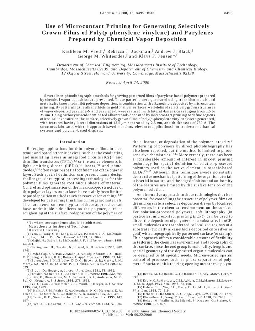
Use of Microcontact Printing for Generating Selectively Grown Films of Poly(p-phenylene vinylene) and Parylenes Prepared by Chemical Vapor Deposition Kathleen M. Vaeth, ² Rebecca J. Jackman, ‡ Andrew J. Black, ‡ George M. Whitesides, ‡ and Klavs F. Jensen* ,² Department of Chemical Engineering, Massachusetts Institute of Technology, Cambridge, Massachusetts 02139, and Department of Chemistry and Chemical Biology, 12 Oxford Street, Harvard University, Cambridge, Massachusetts 02138 Received April 24, 2000 Several non-photolithographic methods for growing patterned films of parylene-based polymers prepared by chemical vapor deposition are presented. These patterns were generated using transition metals and metal salts known to inhibit polymer deposition, in combination with alkanethiols deposited by microcontact printing. By patterning the alkanethiols on gold or silver surfaces, well-defined selectively grown structures of vapor-deposited parylene-N and parylene-C were realized, with lateral dimensions ranging from 1.5 to 35 μm. Using carboxylic acid-terminated alkanethiols deposited by microcontact printing to define regions of iron salt exposure on the surface, selectively grown films of poly(p-phenylene vinylene) were generated, with features having lateral dimensions of 12.5 μm separated by 2.5 μm, and thicknesses of 750 Å. The structures fabricated with this approach have dimensions relevant to applications in microelectromechanical systems and polymer-based displays. Introduction Emerging applications for thin polymer films in elec- tronic and optoelectronic devices, such as the conducting and insulating layers in integrated circuits (ICs) 1,2 and thin film transistors (TFTs), 3,4 or the active elements in light emitting diodes (LEDs), 5,6 lasers, 7,8 and photo- diodes, 9,10 often require spatial confinement of the organic layer. Such spatial definition can present many design challenges, since typical processing technologies for thin polymer films generate continuous sheets of material. Control and optimization of the macroscopic structure of thin polymer layers on surfaces have mainly been limited to postdeposition methods such as reactive ion etching 11,12 developed for patterning thin films of inorganic materials. The harsh environments typical of these approaches can have undesirable side effects on the polymer, such as roughening of the surface, redeposition of the polymer on the substrate, or degradation of the polymer integrity. 2 Patterning of polymers by direct photolithography has also been reported, but the method is limited to photo- sensitive chemistries. 13,14 More recently, there has been a considerable amount of interest in ink-jet printing technology for spatial definition of solution-processed polymers used as the active element in organic-based LEDs. 15-17 Although this technique avoids potentially destructive mechanical patterning of the organic material, it is serial in nature, and the edge definition and uniformity of the features are limited by the surface tension of the polymer solution. An alternative approach to these technologies that has potential for controlling the structure of polymer films on the micron scale is selective deposition driven by localized differences in the chemical environment on the surface. For solution-processed polymers, soft lithography (in particular, microcontact printing (μCP)), can be used to direct the deposition of polymers on a substrate. In μCP, small molecules are transferred to localized regions of a substrate (typically alkanethiols deposited onto silver or gold) with a topographically patterned surface (or stamp). This approach offers a considerable amount of flexibility in tailoring the chemical environment and topography of the surface, since the end group functionality, length, and spatial geometry of the deposited organic molecules can be designed to fit specific needs. Micron-scaled spatial control of processes such as phase-separation of poly- mers, 18 surface-initiated ring-opening metathesis polym- * To whom correspondence should be addressed. ² Massachusetts Institute of Technology. ‡ Harvard University. (1) You, L.; Yang, G. R.; Lang, C. I.; Wu, P.; Moore, J. A.; McDonald, J. F.; Lu, T. M. J. Vac. Sci. Technol. A 1993, 11, 3047. (2) Majid, N.; Dabral, S.; McDonald, J. F. J. Electron. Mater. 1988, 18, 301. (3) Sirringhaus, H.; Tessler, N.; Friend, R. H. Science 1998, 280, 1741. (4) Dodabalapur, A.; Bao, Z.; Makhija, A.; Laquindanum, J. G.; Raju, V. R.; Feng, Y.; Katz, H. E.; Rogers, J. Appl. Phys. Lett. 1998, 73, 142. (5) Burroughes, J. H.; Bradley, D. D. C.; Brown, A. R.; Marks, R. N.; Macay, K.; Friend, R. H.; Burns, P. L.; Holmes, A. B. Nature 1990, 347, 539. (6) Braun, D.; Heeger, A. J. Appl. Phys. Lett. 1991, 58, 1982. (7) Tessler, N.; Denton, G. J.; Friend, R. H. Nature 1996, 382, 695. (8) Hide, F.; Diaz-Garcia, M. A.; Schwartz, B. J.; Andersson, M. R.; Pei, Q.; Heeger, A. J. Science 1996, 273, 1833. (9) Yu, G.; Gao, J.; Hummelen, J. C.; Wudl, F.; Heeger, A. J. Science 1995, 270, 1789. (10) Halls, J. J. M.; Walsh, C. A.; Greenham, N. C.; Marseglia, E. A.; Friend, R. H.; Moratti, S. C.; Holmes, A. B. Nature 1995, 376, 498. (11) Tacito, R. D.; Steinbruchel, C. J. Electrochem. Soc. 1995, 143, 1974. (12) Yeh, J. T. C.; Grebe, K. R. J. Vac. Sci. Technol. 1983, A1, 604. (13) Renak, M. L.; Bazon, G. C.; Roitman, D. Adv. Mater. 1997, 9, 392. (14) Drury, C. J.; Mutsaers, C. M. J.; Hart, C. M.; Matters, M.; Leeuw, D. M. D. Appl. Phys. Lett. 1998, 73, 108. (15) Hebner, T. R.; Wu, C. C.; Marcy, D.; Lu, M. H.; Sturm, J. C. Appl. Phys. Lett. 1998, 72, 519. (16) Hebner, T. R.; Sturm, J. C. Appl. Phys. Lett. 1998, 73, 1775. (17) Bharathan, J.; Yang, Y. Appl. Phys. Lett. 1998,72, 2660. (18) Boltau, M.; Walheim, S.; Mlynek, J.; Krausch, G.; Steiner, U. Nature 1998, 391, 877. 8495 Langmuir 2000, 16, 8495-8500 10.1021/la000602w CCC: $19.00 © 2000 American Chemical Society Published on Web 09/22/2000
Transcript of Use of Microcontact Printing for Generating Selectively ... · Use of Microcontact Printing for...
Use of Microcontact Printing for Generating SelectivelyGrown Films of Poly(p-phenylene vinylene) and Parylenes
Prepared by Chemical Vapor Deposition
Kathleen M. Vaeth,† Rebecca J. Jackman,‡ Andrew J. Black,‡George M. Whitesides,‡ and Klavs F. Jensen*,†
Department of Chemical Engineering, Massachusetts Institute of Technology,Cambridge, Massachusetts 02139, and Department of Chemistry and Chemical Biology,
12 Oxford Street, Harvard University, Cambridge, Massachusetts 02138
Received April 24, 2000
Several non-photolithographic methods for growing patterned films of parylene-based polymers preparedby chemical vapor deposition are presented. These patterns were generated using transition metals andmetal salts known to inhibit polymer deposition, in combination with alkanethiols deposited by microcontactprinting. By patterning the alkanethiols on gold or silver surfaces, well-defined selectively grown structuresof vapor-deposited parylene-N and parylene-C were realized, with lateral dimensions ranging from 1.5 to35 µm. Using carboxylic acid-terminated alkanethiols deposited by microcontact printing to define regionsof iron salt exposure on the surface, selectively grown films of poly(p-phenylene vinylene) were generated,with features having lateral dimensions of 12.5 µm separated by 2.5 µm, and thicknesses of 750 Å. Thestructures fabricated with this approach have dimensions relevant to applications in microelectromechanicalsystems and polymer-based displays.
Introduction
Emerging applications for thin polymer films in elec-tronic and optoelectronic devices, such as the conductingand insulating layers in integrated circuits (ICs)1,2 andthin film transistors (TFTs),3,4 or the active elements inlight emitting diodes (LEDs),5,6 lasers,7,8 and photo-diodes,9,10 often require spatial confinement of the organiclayer. Such spatial definition can present many designchallenges, since typical processing technologies for thinpolymer films generate continuous sheets of material.Control and optimization of the macroscopic structure ofthin polymer layers on surfaces have mainly been limitedto postdeposition methods such as reactive ion etching11,12
developed for patterning thin films of inorganic materials.The harsh environments typical of these approaches canhave undesirable side effects on the polymer, such asroughening of the surface, redeposition of the polymer on
the substrate, or degradation of the polymer integrity.2Patterning of polymers by direct photolithography hasalso been reported, but the method is limited to photo-sensitive chemistries.13,14 More recently, there has beena considerable amount of interest in ink-jet printingtechnology for spatial definition of solution-processedpolymers used as the active element in organic-basedLEDs.15-17 Although this technique avoids potentiallydestructive mechanical patterning of the organic material,it is serial in nature, and the edge definition and uniformityof the features are limited by the surface tension of thepolymer solution.
An alternative approach to these technologies that haspotential for controlling the structure of polymer films onthe micron scale is selective deposition driven by localizeddifferences in the chemical environment on the surface.For solution-processed polymers, soft lithography (inparticular, microcontact printing (µCP)), can be used todirect the deposition of polymers on a substrate. In µCP,small molecules are transferred to localized regions of asubstrate (typically alkanethiols deposited onto silver orgold) with a topographically patterned surface (or stamp).This approach offers a considerable amount of flexibilityin tailoring the chemical environment and topography ofthe surface, since the end group functionality, length, andspatial geometry of the deposited organic molecules canbe designed to fit specific needs. Micron-scaled spatialcontrol of processes such as phase-separation of poly-mers,18 surface-initiated ring-opening metathesis polym-
* To whom correspondence should be addressed.† Massachusetts Institute of Technology.‡ Harvard University.(1) You, L.; Yang, G. R.; Lang, C. I.; Wu, P.; Moore, J. A.; McDonald,
J. F.; Lu, T. M. J. Vac. Sci. Technol. A 1993, 11, 3047.(2) Majid, N.; Dabral, S.; McDonald, J. F. J. Electron. Mater. 1988,
18, 301.(3) Sirringhaus, H.; Tessler, N.; Friend, R. H. Science 1998, 280,
1741.(4) Dodabalapur, A.; Bao, Z.; Makhija, A.; Laquindanum, J. G.; Raju,
V. R.; Feng, Y.; Katz, H. E.; Rogers, J. Appl. Phys. Lett. 1998, 73, 142.(5) Burroughes, J. H.; Bradley, D. D. C.; Brown, A. R.; Marks, R. N.;
Macay, K.; Friend, R. H.; Burns, P. L.; Holmes, A. B. Nature 1990, 347,539.
(6) Braun, D.; Heeger, A. J. Appl. Phys. Lett. 1991, 58, 1982.(7) Tessler, N.; Denton, G. J.; Friend, R. H. Nature 1996, 382, 695.(8) Hide, F.; Diaz-Garcia, M. A.; Schwartz, B. J.; Andersson, M. R.;
Pei, Q.; Heeger, A. J. Science 1996, 273, 1833.(9) Yu, G.; Gao, J.; Hummelen, J. C.; Wudl, F.; Heeger, A. J. Science
1995, 270, 1789.(10) Halls, J. J. M.; Walsh, C. A.; Greenham, N. C.; Marseglia, E. A.;
Friend, R. H.; Moratti, S. C.; Holmes, A. B. Nature 1995, 376, 498.(11) Tacito, R. D.; Steinbruchel, C. J. Electrochem. Soc. 1995, 143,
1974.(12) Yeh, J. T. C.; Grebe, K. R. J. Vac. Sci. Technol. 1983, A1, 604.
(13) Renak, M. L.; Bazon, G. C.; Roitman, D. Adv. Mater. 1997, 9,392.
(14) Drury, C. J.; Mutsaers, C. M. J.; Hart, C. M.; Matters, M.; Leeuw,D. M. D. Appl. Phys. Lett. 1998, 73, 108.
(15) Hebner, T. R.; Wu, C. C.; Marcy, D.; Lu, M. H.; Sturm, J. C. Appl.Phys. Lett. 1998, 72, 519.
(16) Hebner, T. R.; Sturm, J. C. Appl. Phys. Lett. 1998, 73, 1775.(17) Bharathan, J.; Yang, Y. Appl. Phys. Lett. 1998, 72, 2660.(18) Boltau, M.; Walheim, S.; Mlynek, J.; Krausch, G.; Steiner, U.
Nature 1998, 391, 877.
8495Langmuir 2000, 16, 8495-8500
10.1021/la000602w CCC: $19.00 © 2000 American Chemical SocietyPublished on Web 09/22/2000
erization,19 selective deposition of polyelectrolytes bysequential self-adsorption,20 electroless deposition,21 andelectrodeposition22 of conducting polymers have beenachieved using surfaces patterned by µCP.
Recently, we reported a novel method for realizingselective growth of parylene and its derivatives preparedby chemical vapor deposition (CVD).23,24 Specifically, wehave discovered that deposition of the electroluminescent(EL) polymer poly(p-phenylene vinylene) (PPV), as wellas parylene-N and parylene-C all prepared by CVD, isinhibited by several transition metals, metal salts, andorganometallic complexes, such as those based on iron,ruthenium, platinum, palladium, silver, copper, and gold.(PPV is of interest for use in polymer-based LEDs5 andlasers,7 and the parylenes are of interest for multi-leveledICs1 and biopassivation coatings.25) Although the exactmechanism by which inhibition occurs is not known, ourstudies suggest that the effect of the metal is to deactivatethe p-xylylene reactive intermediate characteristic ofparylene chemistry in such a way that the molecule isprevented from participating in the nucleation andpropagation reactions of polymerization.24 Evaporatedmetals, metal salts, and organometallic complexes haveall been found to prevent the deposition of the CVDpolymers, but well-defined selectively grown CVD polymerfeatures with lateral dimensions on the order of a fewmicrons have only been realized with evaporated metalspatterned on surfaces by photolithography.24 In this report,we present several non-photolithographic methods that
can be used for fabrication of patterned parylene-basedCVD polymer films. These methods use transition metalsalts and evaporated transition metal layers in combina-tion with µCP to activate or deactivate regions of thesurface to polymer growth. We have used this method togenerate patterned CVD polymer films with featuresranging from 1.5 to 35 µm in width.
Experimental Section
The polymer CVD reaction system used in these studies hasbeen described previously.25 Parylene-N and parylene-C wereprepared from [2.2]paracyclophane (Sigma-Aldrich) and dichloro-[2.2]paracyclophane (courtesy of Specialty Coating Systems)monomers, respectively, and R,R′-dichloro-p-xylene (Aldrich) wasused for PPV deposition. All monomers were pyrolized at 675 °Cand 0.05 Torr to form p-xylylene (which is the reactive monomerfor polymerization) or a p-xylylene derivative.27,28 The films weredeposited at 10 Å/s and 25 °C onto silicon(100) surfaces metallizedwith silver (400 Å thick deposited at 10 Å/s) or gold (50 Åchromium adhesion layer at 2 Å/s, followed by 200 Å thick goldlayer deposited at 5 Å/s).
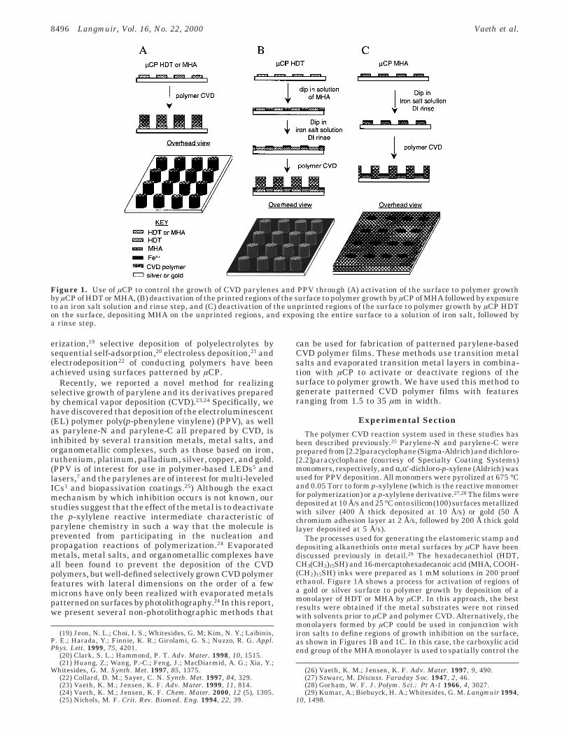
The processes used for generating the elastomeric stamp anddepositing alkanethiols onto metal surfaces by µCP have beendiscussed previously in detail.29 The hexadecanethiol (HDT,CH3(CH2)15SH) and 16-mercaptohexadecanoic acid (MHA, COOH-(CH2)15SH) inks were prepared as 1 mM solutions in 200 proofethanol. Figure 1A shows a process for activation of regions ofa gold or silver surface to polymer growth by deposition of amonolayer of HDT or MHA by µCP. In this approach, the bestresults were obtained if the metal substrates were not rinsedwith solvents prior to µCP and polymer CVD. Alternatively, themonolayers formed by µCP could be used in conjunction withiron salts to define regions of growth inhibition on the surface,as shown in Figures 1B and 1C. In this case, the carboxylic acidend group of the MHA monolayer is used to spatially control the
(19) Jeon, N. L.; Choi, I. S.; Whitesides, G. M; Kim, N. Y.; Laibinis,P. E.; Harada, Y.; Finnie, K. R.; Girolami, G. S.; Nuzzo, R. G. Appl.Phys. Lett. 1999, 75, 4201.
(20) Clark, S. L.; Hammond, P. T. Adv. Mater. 1998, 10, 1515.(21) Huang, Z.; Wang, P.-C.; Feng, J.; MacDiarmid, A. G.; Xia, Y.;
Whitesides, G. M. Synth. Met. 1997, 85, 1375.(22) Collard, D. M.; Sayer, C. N. Synth. Met. 1997, 84, 329.(23) Vaeth, K. M.; Jensen, K. F. Adv. Mater. 1999, 11, 814.(24) Vaeth, K. M.; Jensen, K. F. Chem. Mater. 2000, 12 (5), 1305.(25) Nichols, M. F. Crit. Rev. Biomed. Eng. 1994, 22, 39.
(26) Vaeth, K. M.; Jensen, K. F. Adv. Mater. 1997, 9, 490.(27) Szwarc, M. Discuss. Faraday Soc. 1947, 2, 46.(28) Gorham, W. F. J. Polym. Sci.: Pt A-1 1966, 4, 3027.(29) Kumar, A.; Biebuyck, H. A.; Whitesides, G. M. Langmuir 1994,
10, 1498.
Figure 1. Use of µCP to control the growth of CVD parylenes and PPV through (A) activation of the surface to polymer growthby µCP of HDT or MHA, (B) deactivation of the printed regions of the surface to polymer growth by µCP of MHA followed by exposureto an iron salt solution and rinse step, and (C) deactivation of the unprinted regions of the surface to polymer growth by µCP HDTon the surface, depositing MHA on the unprinted regions, and exposing the entire surface to a solution of iron salt, followed bya rinse step.
8496 Langmuir, Vol. 16, No. 22, 2000 Vaeth et al.
deposition of iron salts on the surface, which are known to inhibitCVD polymer growth. This approach is particularly flexible, sincethe MHA could be printed directly onto the surface with thestamp (Figure 1B), or deposited in the unprinted regions afterµCP an alkanethiol with an end group that does not interactwith the iron salt, such as HDT (Figure 1C). In this way, bothdiscrete polymer structures and discrete “holes” in a continuouspolymer film could be fabricated using a stamp formed from asingle master. Association of the iron salt with the carboxylicacid end group of MHA was performed by dipping the printedsubstrate into an aqueous iron sulfate or iron(III) chloride solution(0.2 mg/mL in deionized water) for 20 s and then running a streamof deionized water over the surface for 10 s.
The structure of the patterned CVD polymer films wasanalyzed with a Digital Nanoscope 3000 atomic force microscope(AFM) in tapping mode, and film thicknesses were measuredwith a P-10 profilometer with a tip radius of 2 µm. Fouriertransform infrared reflection-absorption spectroscopy (IRRAS)was performed with a Nicolet 800 spectrometer.
Results and Discussion
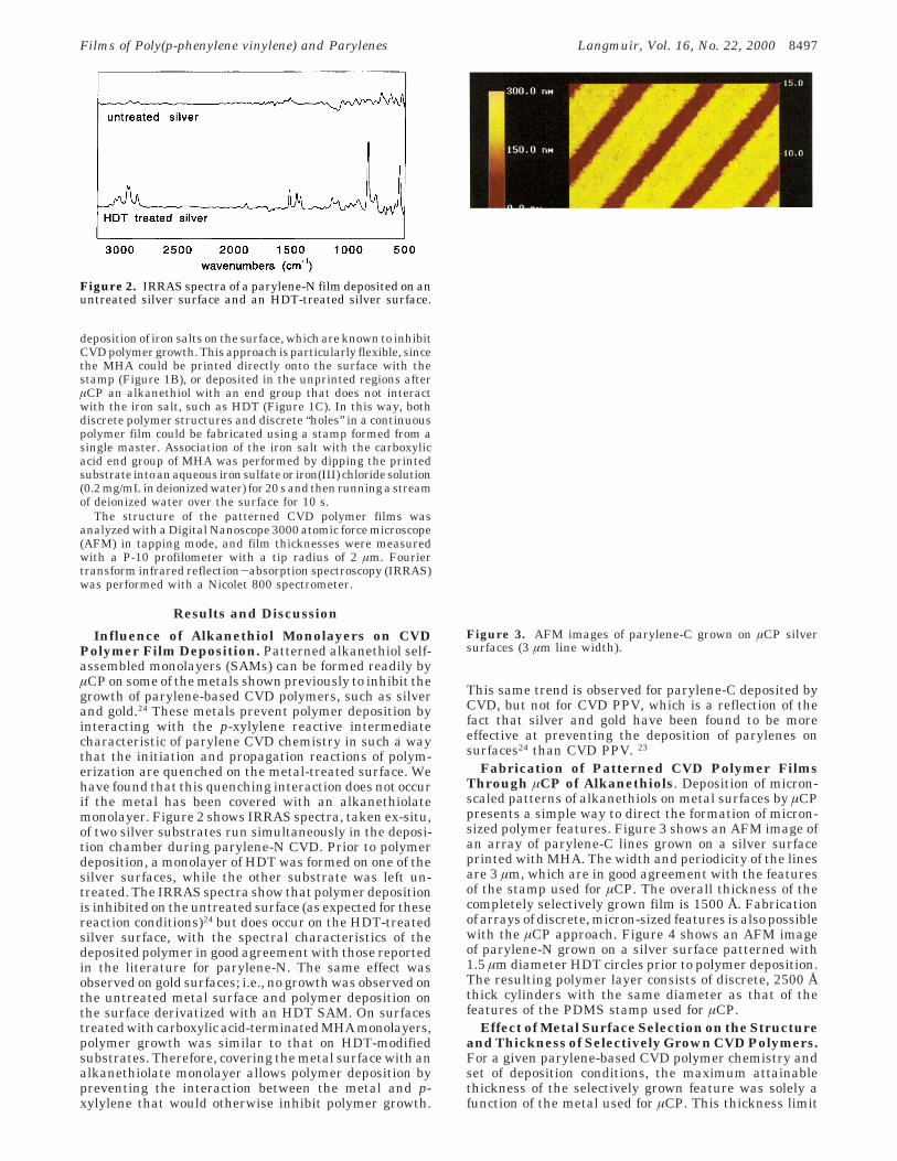
Influence of Alkanethiol Monolayers on CVDPolymer Film Deposition. Patterned alkanethiol self-assembled monolayers (SAMs) can be formed readily byµCP on some of the metals shown previously to inhibit thegrowth of parylene-based CVD polymers, such as silverand gold.24 These metals prevent polymer deposition byinteracting with the p-xylylene reactive intermediatecharacteristic of parylene CVD chemistry in such a waythat the initiation and propagation reactions of polym-erization are quenched on the metal-treated surface. Wehave found that this quenching interaction does not occurif the metal has been covered with an alkanethiolatemonolayer. Figure 2 shows IRRAS spectra, taken ex-situ,of two silver substrates run simultaneously in the deposi-tion chamber during parylene-N CVD. Prior to polymerdeposition, a monolayer of HDT was formed on one of thesilver surfaces, while the other substrate was left un-treated. The IRRAS spectra show that polymer depositionis inhibited on the untreated surface (as expected for thesereaction conditions)24 but does occur on the HDT-treatedsilver surface, with the spectral characteristics of thedeposited polymer in good agreement with those reportedin the literature for parylene-N. The same effect wasobserved on gold surfaces; i.e., no growth was observed onthe untreated metal surface and polymer deposition onthe surface derivatized with an HDT SAM. On surfacestreated with carboxylic acid-terminated MHA monolayers,polymer growth was similar to that on HDT-modifiedsubstrates. Therefore, covering the metal surface with analkanethiolate monolayer allows polymer deposition bypreventing the interaction between the metal and p-xylylene that would otherwise inhibit polymer growth.
This same trend is observed for parylene-C deposited byCVD, but not for CVD PPV, which is a reflection of thefact that silver and gold have been found to be moreeffective at preventing the deposition of parylenes onsurfaces24 than CVD PPV. 23
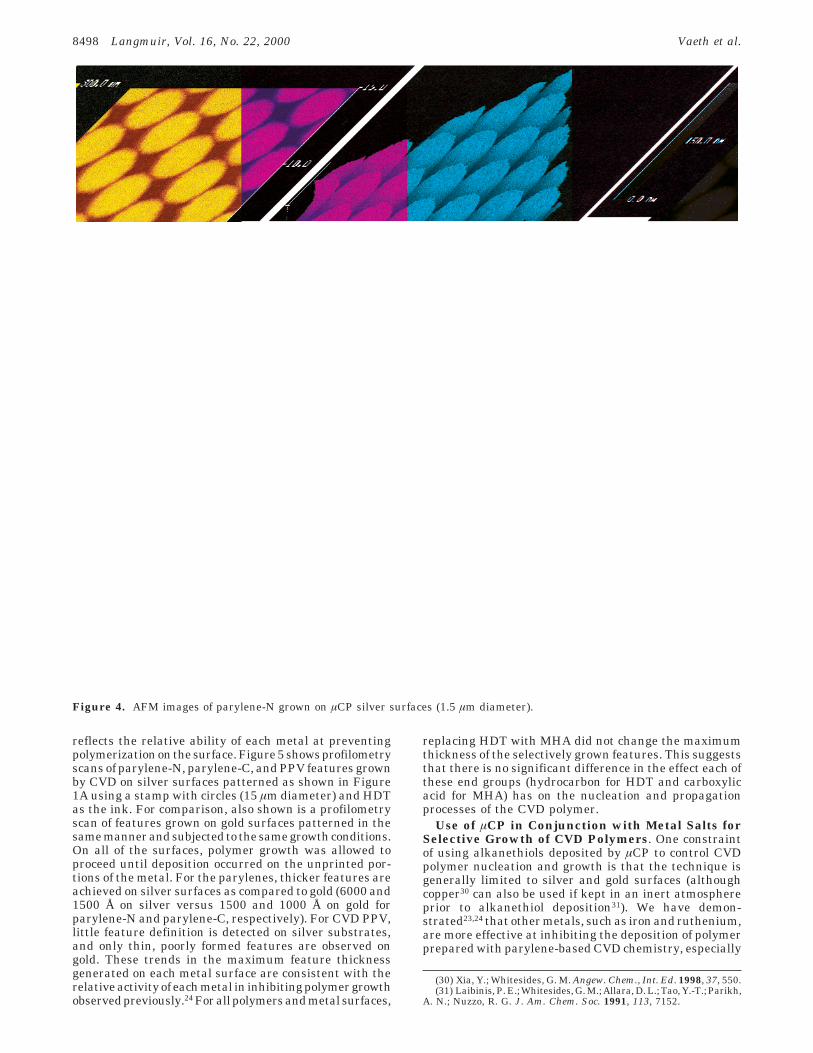
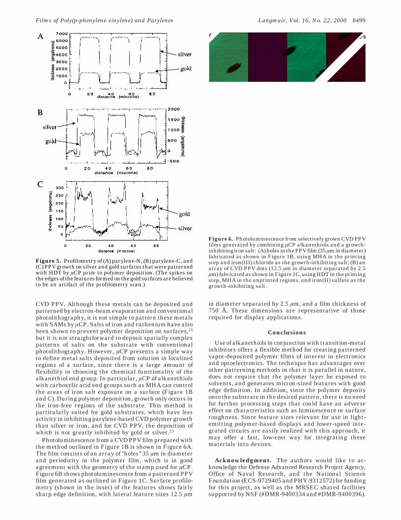
Fabrication of Patterned CVD Polymer FilmsThrough µCP of Alkanethiols. Deposition of micron-scaled patterns of alkanethiols on metal surfaces by µCPpresents a simple way to direct the formation of micron-sized polymer features. Figure 3 shows an AFM image ofan array of parylene-C lines grown on a silver surfaceprinted with MHA. The width and periodicity of the linesare 3 µm, which are in good agreement with the featuresof the stamp used for µCP. The overall thickness of thecompletely selectively grown film is 1500 Å. Fabricationof arrays of discrete, micron-sized features is also possiblewith the µCP approach. Figure 4 shows an AFM imageof parylene-N grown on a silver surface patterned with1.5 µm diameter HDT circles prior to polymer deposition.The resulting polymer layer consists of discrete, 2500 Åthick cylinders with the same diameter as that of thefeatures of the PDMS stamp used for µCP.
Effect of Metal Surface Selection on the Structureand Thickness of Selectively Grown CVD Polymers.For a given parylene-based CVD polymer chemistry andset of deposition conditions, the maximum attainablethickness of the selectively grown feature was solely afunction of the metal used for µCP. This thickness limit
Figure 2. IRRAS spectra of a parylene-N film deposited on anuntreated silver surface and an HDT-treated silver surface.
Figure 3. AFM images of parylene-C grown on µCP silversurfaces (3 µm line width).
Films of Poly(p-phenylene vinylene) and Parylenes Langmuir, Vol. 16, No. 22, 2000 8497
reflects the relative ability of each metal at preventingpolymerization on the surface. Figure 5 shows profilometryscans of parylene-N, parylene-C, and PPV features grownby CVD on silver surfaces patterned as shown in Figure1A using a stamp with circles (15 µm diameter) and HDTas the ink. For comparison, also shown is a profilometryscan of features grown on gold surfaces patterned in thesame manner and subjected to the same growth conditions.On all of the surfaces, polymer growth was allowed toproceed until deposition occurred on the unprinted por-tions of the metal. For the parylenes, thicker features areachieved on silver surfaces as compared to gold (6000 and1500 Å on silver versus 1500 and 1000 Å on gold forparylene-N and parylene-C, respectively). For CVD PPV,little feature definition is detected on silver substrates,and only thin, poorly formed features are observed ongold. These trends in the maximum feature thicknessgenerated on each metal surface are consistent with therelative activity of each metal in inhibiting polymer growthobserved previously.24 For all polymers and metal surfaces,
replacing HDT with MHA did not change the maximumthickness of the selectively grown features. This suggeststhat there is no significant difference in the effect each ofthese end groups (hydrocarbon for HDT and carboxylicacid for MHA) has on the nucleation and propagationprocesses of the CVD polymer.
Use of µCP in Conjunction with Metal Salts forSelective Growth of CVD Polymers. One constraintof using alkanethiols deposited by µCP to control CVDpolymer nucleation and growth is that the technique isgenerally limited to silver and gold surfaces (althoughcopper30 can also be used if kept in an inert atmosphereprior to alkanethiol deposition31). We have demon-strated23,24 that other metals, such as iron and ruthenium,are more effective at inhibiting the deposition of polymerprepared with parylene-based CVD chemistry, especially
(30) Xia, Y.; Whitesides, G. M. Angew. Chem., Int. Ed. 1998, 37, 550.(31) Laibinis, P. E.; Whitesides, G. M.; Allara, D. L.; Tao, Y.-T.; Parikh,
A. N.; Nuzzo, R. G. J. Am. Chem. Soc. 1991, 113, 7152.
Figure 4. AFM images of parylene-N grown on µCP silver surfaces (1.5 µm diameter).
8498 Langmuir, Vol. 16, No. 22, 2000 Vaeth et al.
CVD PPV. Although these metals can be deposited andpatterned by electron-beam evaporation and conventionalphotolithography, it is not simple to pattern these metalswith SAMs by µCP. Salts of iron and ruthenium have alsobeen shown to prevent polymer deposition on surfaces,23
but it is not straightforward to deposit spatially complexpatterns of salts on the substrate with conventionalphotolithography. However, µCP presents a simple wayto define metal salts deposited from solution in localizedregions of a surface, since there is a large amount offlexibility in choosing the chemical functionality of thealkanethiol end group. In particular, µCP of alkanethiolswith carboxylic acid end groups such as MHA can controlthe areas of iron salt exposure on a surface (Figure 1Band C). During polymer deposition, growth only occurs inthe iron-free regions of the substrate. This method isparticularly suited for gold substrates, which have lessactivity in inhibiting parylene-based CVD polymer growththan silver or iron, and for CVD PPV, the deposition ofwhich is not greatly inhibited by gold or silver.23
Photoluminescence from a CVD PPV film prepared withthe method outlined in Figure 1B is shown in Figure 6A.The film consists of an array of "holes” 35 µm in diameterand periodicity in the polymer film, which is in goodagreement with the geometry of the stamp used for µCP.Figure 6B shows photoluminescence from a patterned PPVfilm generated as outlined in Figure 1C. Surface profilo-metry (shown in the inset) of the features shows fairlysharp edge definition, with lateral feature sizes 12.5 µm
in diameter separated by 2.5 µm, and a film thickness of750 Å. These dimensions are representative of thoserequired for display applications.
Conclusions
Use of alkanethiols in conjunction with transition-metalinhibitors offers a flexible method for creating patternedvapor-deposited polymer films of interest in electronicsand optoelectronics. The technique has advantages overother patterning methods in that it is parallel in nature,does not require that the polymer layer be exposed tosolvents, and generates micron-sized features with goodedge definition. In addition, since the polymer depositsonto the substrate in the desired pattern, there is no needfor further processing steps that could have an adverseeffect on characteristics such as luminescence or surfaceroughness. Since feature sizes relevant for use in light-emitting polymer-based displays and lower-speed inte-grated circuits are easily realized with this approach, itmay offer a fast, low-cost way for integrating thesematerials into devices.
Acknowledgment. The authors would like to ac-knowledge the Defense Advanced Research Project Agency,Office of Naval Research, and the National ScienceFoundation (ECS-9729405 and PHY-9312572) for fundingfor this project, as well as the MRSEC shared facilitiessupported by NSF (#DMR-9400334 and #DMR-9400396).
Figure 5. Profilometry of (A) parylene-N, (B) parylene-C, and(C) PPV growth on silver and gold surfaces that were patternedwith HDT by µCP prior to polymer deposition. (The spikes onthe edges of the features formed on the gold surfaces are believedto be an artifact of the profilometry scan.)
Figure 6. Photoluminescence from selectively grown CVD PPVfilms generated by combining µCP alkanethiols and a growth-inhibiting iron salt: (A) holes in the PPV film (35µm in diameter)fabricated as shown in Figure 1B, using MHA in the printingstep and iron(III) chloride as the growth-inhibiting salt; (B) anarray of CVD PPV dots (12.5 µm in diameter separated by 2.5µm) fabricated as shown in Figure 1C, using HDT in the printingstep, MHA in the unprinted regions, and iron(II) sulfate as thegrowth-inhibiting salt.
Films of Poly(p-phenylene vinylene) and Parylenes Langmuir, Vol. 16, No. 22, 2000 8499

Graduate fellowships from the Fannie and John HertzFoundation (K.M.V.) and Natural Sciences and Engineer-ing Research Council (R.J.J.) are also gratefully acknowl-edged. In addition, we would like to thank Mr. Gale Petrichfor support with the electron-beam evaporator, Alice Jang
for assistance in generating the CVD polymer films, andSpecialty Coating Systems for providing the dichloro[2.2]-paracyclophane monomer.
LA000602W
8500 Langmuir, Vol. 16, No. 22, 2000 Vaeth et al.