Use of laser beam diffraction for non-invasive ... · Use of laser beam diffraction for...
7
•
-
Upload
duongduong -
Category
Documents
-
view
218 -
download
0
Transcript of Use of laser beam diffraction for non-invasive ... · Use of laser beam diffraction for...

Loughborough UniversityInstitutional Repository
Use of laser beamdiffraction for non-invasivecharacterisation of CdTethin film growth structure
This item was submitted to Loughborough University's Institutional Repositoryby the/an author.
Citation: GOFFIN, N.J. ... et al., 2015. Use of laser beam diffraction for non-invasive characterisation of CdTe thin film growth structure. Procedia CIRP37, pp. 101-106.
Additional Information:
• This is an Open Access Article. It is published by Else-vier under the Creative Commons Attribution 4.0 Unported Li-cence (CC BY). Full details of this licence are available at:http://creativecommons.org/licenses/by/4.0/ The paper was also pre-sented at CIRPe 2015 - Understanding the life cycle implications of man-ufacturing, 29th Sept- 1st Oct, 2015.
Metadata Record: https://dspace.lboro.ac.uk/2134/19447
Version: Published
Publisher: c© 2015 The Authors. Published by Elsevier
Rights: This work is made available according to the conditions of the Cre-ative Commons Attribution-NonCommercial-NoDerivatives 4.0 International(CC BY-NC-ND 4.0) licence. Full details of this licence are available at:https://creativecommons.org/licenses/by-nc-nd/4.0/
Please cite the published version.

Procedia CIRP 37 ( 2015 ) 101 – 106
Available online at www.sciencedirect.com
2212-8271 © 2015 The Authors. Published by Elsevier B.V. This is an open access article under the CC BY-NC-ND license (http://creativecommons.org/licenses/by-nc-nd/4.0/).Peer-review under responsibility of the organizing committee of CIRPe 2015 - Understanding the life cycle implications of manufacturingdoi: 10.1016/j.procir.2015.08.077
ScienceDirect
CIRPe 2015 - Understanding the life cycle implications of manufacturing
Use of laser beam diffraction for non-invasive characterisation of CdTe thin film growth structure
Nicholas Goffina, Fabiana Liscob, Alessandro Simeonea, Gianfranco Claudiob, John Tyrerc, ElliotWoolleya*
aCentre for Sustainable Manufacturing and Recycling Technologies (SMART), Wolfson School of Mechanical and Manufacturing Engineering, Loughborough University, LE11 3TU, UK
bCentre for Renewable Energy Systems Technology (CREST), School of Electronic, Electrical and Systems Engineering, Loughborough University, Leicestershire, LE11 3TU, UK
cOptical Engineering Research Group, Wolfson School of Mechanical and Manufacturing Engineering, Loughborough University, LE11 3TU, UK
* Corresponding author. Tel.: +441509225410; E-mail address: [email protected]
Abstract
Characterisation of Cadmium Telluride (CdTe) thin films commonly requires the use of invasive techniques for the identification of their structural growth and the detection of defects which occur during the deposition process. Structural growth and the presence of defects can affect the performance of the final device. A non-invasive inspection system for CdTe films has been developed to identify the structural properties of this material,comparing two different deposition techniques, Close Space Sublimation (CSS) and Magnetron Sputtering (MS).The proposed system utilises a 1 μm diode laser which passes through the CdTe layer, originating detectable diffraction patterns, which are characterised using image processing techniques and assessed using a neural network-based cognitive decision-making support system. Results are found to be consistent with the conventional microscopic techniques (SEM and TEM) used to analyse morphological and structural properties of thin-film CdTe solar cells.
© 2015 The Authors. Published by Elsevier B.V.Selection and peer-review under responsibility of the International Scientific Committee of the “4th CIRP Global Web Conference” in the person of the Conference Chair Dr. John Ahmet Erkoyuncu.Keywords: CdTe; laser diffraction; pattern recognition
1. Introduction
Optical measurement has for a long time been a recognised technique for real-time characterisation of suspended particlesand their size distributions. It has been used in many different fields for example the analysis and control of particulate emissions, automobile exhaust gas [1], solid coal [2]particulates, analysis of aggregate in rivers [3], manufacture of metallic powders and production of pharmaceuticals [4].
The inherent advantage of optical-based systems over other techniques is the fact that they provide in situ and non-invasive measurements [5] for real-time analysis.
A novel application for this technique is in thePhotovoltaics (PV) field, based on the use of a laser beam to compare the structural growth of CdTe solar cells.
This study with its preliminary results shows the potential use and development of this characterisation technique as an in-situ non-invasive manufacturing inspection system.
© 2015 The Authors. Published by Elsevier B.V. This is an open access article under the CC BY-NC-ND license (http://creativecommons.org/licenses/by-nc-nd/4.0/).Peer-review under responsibility of the organizing committee of CIRPe 2015 - Understanding the life cycle implications of manufacturing

102 Nicholas Goffi n et al. / Procedia CIRP 37 ( 2015 ) 101 – 106
Among a wide range of technologies available in the PVmarket and currently used to produce CdTe thin films solar cells, two deposition methods were chosen: Closed Space Sublimation (CSS) and Magnetron Sputtering (MS).
Morphological, optical, structural, electrical properties of CdTe thin films change depending on the deposition technique used to grow them.
One of the common drawbacks associated with the growth of CdS/CdTe thin films is the formation of defects (identified as voids, stacking faults or pinholes) that inevitably affect theperformance of the final working device over its life cycle [6].
Where existing laser measurement is focused on particles suspended in a medium, the internal grain structure and the eventual presence of defects in photovoltaic solar cells are analogous to particles while the CdTe layer itself is analogous to the medium.
Potentially, this means that the structural growth of PV thin films can be detected and characterised by applying the same principles used by laser particle measurement systems.
2. Materials and experimental procedures
2.1. Sample preparation
Fig. 1 shows a schematic of the CdTe solar cell utilised for the experimental campaign in superstrate configuration [7].No metal back contact was applied, in order to allow the laser scanning of the CdTe absorber layer.
The CdTe and the CdS have a thickness of 2 μm and 200 nm respectively. The front contact is made of a 3 mm thick Transparent Electrically Conductive Oxide (TEC10) Fluorine doped tin oxide (FTO) coated glass supplied by NSG-Pilkington.
2.2. Deposition techniques
CdTe/CdS stack thin films were deposited on TEC10substrate.
A ~200 nm n-type CdS layer was deposited followed by ~2layer of CdTe thin film by using two different deposition
techniques: Magnetron sputtering (MS) using a ‘PV Solar’ sputtering system (Power Vision Ltd., Crewe UK) [8] and CSS [9].
Fig. 1. Schematic of a CdTe solar cell utilised in experiments
The CdTe stack thin films were tested by illuminating different areas of ~ 7 x 10 mm = 70 mm2 from each sample (CSS, MS). From each selected area (Specimen), 10 images were acquired and analysed (see Table 1).
2.3. Laser diffraction equipment
The experimental laser setup used for this study is shown in Fig. 2. It consisted of a 50 mW laser emitter with a wavelength of 1 μm, an IR filter to attenuate the beam, the specimen undergoing study and a CCD camera with a resolution of 1024 x 768 pixels for image acquisition.
The laser wavelength was carefully selected to match the transmission spectrum of the material under consideration, as well as the wavelength sensitivity of the CCD sensor. CdTe has very high absorption in the range of wavelengths 0.4 - 0.8 μm [10].
Above 0.85 μm, there is a steep drop in absorptivity, such that above this wavelength CdTe is virtually transparent for all practical purposes. 1 μm is the maximum wavelength of sensitivity for CCD sensors, so a wavelength above this could not be used. As the collimated beam leaves the laser, it is attenuated by the filters in order to not overload the CCD sensor.
The beam passes through the CdTe stack thin films where it is subjected to diffraction and directed afterwards to a CCD sensor.
The diffracted portions of the beam show up on the sensor as an array of diffraction rings surrounding the main laser beam spot. A schematic of this is shown in Fig. 3.
3. Sample Characterisation
3.1. Microscopy techniques
The microstructure of CdTe films was studied with a high resolution field emission gun scanning electron microscope (FEGSEM), Leo 1530 VP FEG-SEM, which provides the ability to visualise surface features of the material with nanometre resolution.
The features and grains size have been calculated by using a Microscope Software AxioVision LE (http://www.zeiss.com/microscopy).
The measured grain size was based on a mathematical average over 20 different grains.
Table 1; Experimental ProgrammeSample deposition technique
Specimen ID No. of images per specimen
CSSCSS_1 10CSS_2 10CSS_3 10
MS
MS_1 10MS_2 10MS_3 10MS_4 10MS_5 10
Total 80 images
103 Nicholas Goffi n et al. / Procedia CIRP 37 ( 2015 ) 101 – 106
Laser spot Diffraction rings
A dual beam FEI Nova 600 Nanolab was employed to prepare the samples for transmission electron microscopy (TEM) analysis.
A standard in situ lift off method was used to prepare cross sectional samples and TEM images were acquired using a Jeol JEM 2000FX operating at 200kV, with an integrated camera above the phosphor screen to obtain digital images.
3.2. SEM and optical microscopy characterisation
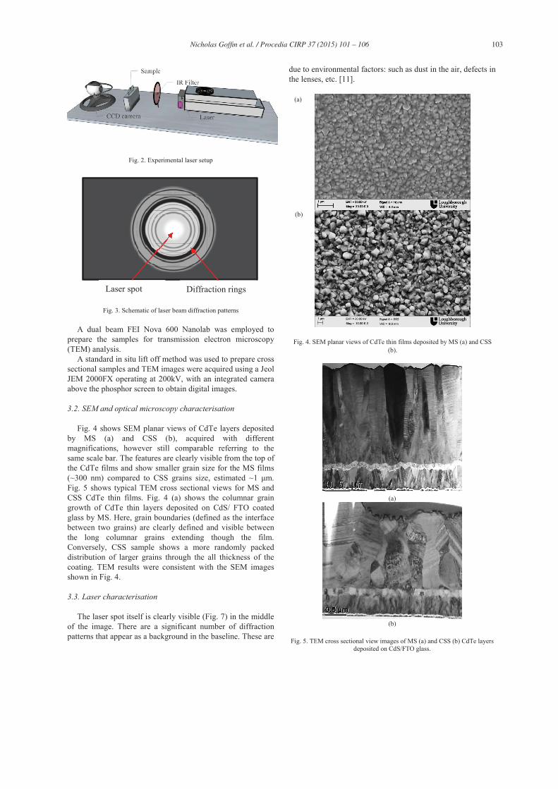
Fig. 4 shows SEM planar views of CdTe layers deposited by MS (a) and CSS (b), acquired with different magnifications, however still comparable referring to the same scale bar. The features are clearly visible from the top of the CdTe films and show smaller grain size for the MS films (~300 nm) compared to CSS grains .Fig. 5 shows typical TEM cross sectional views for MS and CSS CdTe thin films. Fig. 4 (a) shows the columnar grain growth of CdTe thin layers deposited on CdS/ FTO coated glass by MS. Here, grain boundaries (defined as the interface between two grains) are clearly defined and visible between the long columnar grains extending though the film.Conversely, CSS sample shows a more randomly packed distribution of larger grains through the all thickness of the coating. TEM results were consistent with the SEM images shown in Fig. 4.
3.3. Laser characterisation
The laser spot itself is clearly visible (Fig. 7) in the middle of the image. There are a significant number of diffraction patterns that appear as a background in the baseline. These are
due to environmental factors: such as dust in the air, defects in the lenses, etc. [11].
(a)
(b)
Fig. 4. SEM planar views of CdTe thin films deposited by MS (a) and CSS (b).
(a)
(b)
Fig. 5. TEM cross sectional view images of MS (a) and CSS (b) CdTe layers deposited on CdS/FTO glass.
Fig. 2. Experimental laser setup
Fig. 3. Schematic of laser beam diffraction patterns

104 Nicholas Goffi n et al. / Procedia CIRP 37 ( 2015 ) 101 – 106
4. Image processing and decision making
4.1. Baseline image processing
Using the experimental setup illustrated in Fig. 2, a series of 20 images was acquired in the absence of any specimen[12], to be used as a baseline. Having no specimen was equivalent to having a reference blank signal.
Each image was converted to greyscale by eliminating the hue and saturation information while retaining the luminance [13]. The 20 images were then averaged [14] and the resultant average baseline image is reported in Fig. 7.
4.2. Sample image processing
The image processing technique described in Fig. 6 was applied to the 80 image instances (Table 1).
The first step was the RGB-to-greyscale conversion [13].Subsequently, for each image, a subtraction procedure [15][16] was implemented by subtracting the average baseline image from the specimen image. An example of the greyscale raw image for each sample is reported in Fig. 8.
Due to the presence of negative pixel values, it was necessary to normalise [15] each image’s pixel values between a range of 0 to 1 to visualise the subtracted image. Two examples of the resulting images are reported in Fig. 9,both for the CSS and MS samples.
For the 80 normalised images, individual histograms werecomputed and compiled, giving an 80 x 256 matrix dataset(Table 2). Two example histogram plots are reported in Fig.10, for CSS and MS respectively. In this figure, the histograms visually demonstrate the shape and value differences between the two images.
4.3. Feature extraction
Features are defined as a function of one or more measurements, each of which specifies some quantifiable property of an image and is computed such that it quantifies some significant characteristics of the image [17].
A feature extraction procedure was applied to the 80 digital images by calculating the following statistical parameters [18]from the images’ histograms:
Weighted mean (WM)Threshold (T) [19]Variance (Var)Skewness (Skew)Kurtosis (Kurt)
These five statistical features were combined into an 80 x 5 histogram feature matrix (Table 3) to be input into a Neural Network (NN) based decision making system [20][21].
Fig. 6. Image processing flow chart
b
Fig. 7. Average baseline
(a)
(b)
Fig.8. Raw (greyscale) images of CSS(a) MS (b) specimens
Table 3. Histogram feature matrixID test WM T Var Skew Kurt
CSS_1_01 0.3648 0.3451 50734200.9961 9.1107 110.8816CSS_1_02 0.3649 0.3451 48767713.1059 8.6926 102.1713… … … … … …MS_5_10 0.4934 0.4549 25237350.6510 2.4664 9.5437
6. Features extraction6 F i
5. Image histogram5 I hi
4. Image normalisation4 I li i
3. Image subtraction3 I b i
2. Grayscale Image2 G l I
1. RGB Image
b
Table 2. Histogram values of the 80 image instances
Test IDHistogram No. of pixels per shade of grey
0 1 2 … 255
CSS_1_01 1066 987 186 … 488
CSS_1_02 1094 900 254 … 453
… … … … … …
MS_5_10 27 371 753 … 275
105 Nicholas Goffi n et al. / Procedia CIRP 37 ( 2015 ) 101 – 106
(a)
(b)Fig. 9. Normalised subtracted image for CSS (a) and MS (b) samples
hFig. 10. Comparison of two image histograms,
Fig. 11. NN scheme using 5-10-1 nodes configuration
4.4. Pattern recognition
NN pattern recognition based on statistical features [18]extracted from the histograms was utilised for decision making based on the different grain and structural growth of the material.
Two different datasets were built for this NN classification problem: the input and the target matrices. The input matrix is made of 80 rows representing the image instances and 5 columns representing the features. The target vector has two different values: zeros for the more packed and large structureand ones for the columnar and smaller grains growth.
Taking into account the microscope characterisation testresults (see Section 3.2) it is possible to classify the two categories as follows:
CSS specimens: larger grains – denser structureMS specimens: smaller grains-columnar structure.
A three-layer feed-forward back-propagation NN [20] was built with the following configuration: input layer with five nodes that correspond to the number of input feature vector elements [22]; hidden layer with ten nodes. The output layer has only one node containing a coded value (0/1) corresponding to the different grain structure of the samples.The NN scheme is reported in Fig. 11.
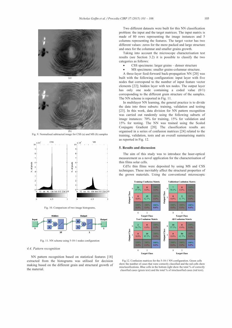
In multilayer NN learning, the general practice is to divide the data into three subsets: training, validation and testing [23]. In this work, data division for NN pattern recognition was carried out randomly using the following subsets of image instances: 70% for training, 15% for validation and 15% for testing. The NN was trained using the Scaled Conjugate Gradient [20]. The classification results are organised in a series of confusion matrices [24] related to the training, validation, tests and an overall summarising matrix as reported in Fig. 12.
5. Results and discussion
The aim of this study was to introduce the laser-optical measurement as a novel application for the characterisation of thin films solar cells.
CdTe thin films were deposited by using MS and CSS techniques. These inevitably affect the structural properties of the grown materials. Using the conventional microscopic
Fig.12. Confusion matrices for the 5-10-1 NN configuration. Green cells
show the number of cases that were correctly classified and the red cells show misclassifications. Blue cells in the bottom right show the total % of correctlyclassified cases (green text) and the total % of misclassified cases (red text).

106 Nicholas Goffi n et al. / Procedia CIRP 37 ( 2015 ) 101 – 106
analyses (SEM and TEM) it was possible to detect a different structural growth between the two samples. CdTe thin films appeared perfectly columnar and characterized by small grains through the thickness of the layer when deposited by MS, while they showed random and packed structure with larger grains size when deposited by CSS. These differences were also detectable using a diffractive laser illuminationtechnique. Both samples produced alterations in the diffraction pattern when compared to the baseline image. The diffraction patterns were consistent between samples deposited with the same technique and the differences between thin films produced with each technique also appeared consistently.
It was found to be possible to quantify these differences using image processing techniques and then to use the results to train a NN decision-making system to recognise them. The overall matrix in Fig. 12 shows how the two categories of samples were successfully classified: larger grains – denser structure and smaller grains-columnar structure without any instances of misclassification.
6. Conclusions
The preliminary following conclusions were drawn from this work:
Shining a 1 μm laser beam through a CdTe/CdS thin film produced additional diffraction patterns that did not occur when no sample was included.Differences in the physical structure due to CSS vs. MS deposition techniques (as demonstrated by SEM and TEM microscopy) produced alterations in the diffraction patterns when the samples were subjected to laser illumination.These differences consistently appeared between different samples and were not a result of random variations in the deposition processes.Image processing techniques and NN decision-making was used to recognise which type of deposition technique was used to deposit CdTe films.SEM and TEM microscopy showed that MS samples were characterized by smaller grains and columnar structure through the all deposited layer while larger and denser, packed structure defined CSS samples. This was reflected in the greater level of diffraction from MS CdTe samples.A correlation therefore existed between the structural growth - grain size of thin films and degree of diffraction, which persisted between samples.
Further work is needed to improve the technique and make it able to identify the presence of defects (voids, stackingfaults, pinholes), which commonly characterised as–deposited CdTe/CdS thin films.
Acknowledgements
The authors are grateful to Professor J.M.Walls from Loughborough University and Dr. K. Barth and Professor W.S. Sampath of the Colorado State University for the supply of CSS deposited thin film CdTe cells using their process of reference.
This research has been funded by the Engineering and Physical Sciences Research Council (EPSRC) in the UK, with project number EP/M014088/1, and carried out as part of the activities of the Centre for Innovative Manufacturing and Industrial Sustainability
References
[1] E. D. Hirleman, J. R. Wittig, and S. L. K. Wittig, “In situ optical measurement of automobile exhaust gas particulate size distributions: regular fuel and methanol mixtures,” Symp. Combust., vol. 16, no. 1, pp. 245–254, 1977.
[2] D. J. Holve, “In Situ Optical Particle Sizing Technique,” J. Energy, vol. 4, no. 4, pp. 176–183, Jul. 1980.
[3] A. J. Bale, “In situ laser optical particle sizing,” J. Sea Res., vol. 36, pp. 31–36, 1996.
[4] D. L. Black, M. Q. McQuay, and M. P. Bonin, “Laser-based techniques for particle-size measurement: A review of sizing methods and their industrial applications,” Prog. Energy Combust. Sci., vol. 22, no. 3, pp. 267–306, 1996.
[5] D. Holve and S. A. Self, “Optical particle sizing for in situ measurements Part 1.,” Appl. Opt., vol. 18, no. 10, pp. 1632–1645, 1979.
[6] A. Romeo, D. L. Ba, H. Zogg, C. Vignali, and A. N. Tiwari, “Influence of CdS growth process on structural and photovoltaic properties of CdTe / CdS solar cells,” vol. 67, pp. 311–321, 2001.
[7] A. N. Tiwari, G. Khrypunov, F. Kurdzesau, D. L. Bätzner, A. Romeo, and H. Zogg, “CdTe solar cell in a novel configuration,” Prog. Photovoltaics Res. Appl., vol. 12, no. 1, pp. 33–38, 2004.
[8] F. Lisco, P. M. Kaminski, A. Abbas, J. W. Bowers, G. Claudio, M. Losurdo, and J. M. Walls, “High rate deposition of thin film cadmium sulphide by pulsed direct current magnetron sputtering,” Thin Solid Films, vol. 574, pp. 43–51, 2015.
[9] V. Manivannan, R. a. Enzenroth, K. L. Barth, S. Kohli, P. R. McCurdy, and W. S. Sampath, “Microstructural features of cadmium telluride photovoltaic thin film devices,” Thin Solid Films, vol. 516, no. 6, pp. 1209–1213, Jan. 2008.
[10] R. O. Bell, “Review of optical applications of CdTe,” Rev. Phys. Appl.,vol. 12, no. 2, pp. 391–399, 1977.
[11] G. B. Parrent and B. J. Thompson, “On the Fraunhofer (Far Field) Diffraction Patterns of Opaque and Transparent Objects with Coherent Background,” Opt. Acta Int. J. Opt., vol. 11, no. 3, pp. 183–193, 1964.
[12] J. C. Stover, is, III. Bellingham, Washington: SPIE, 2012.
[13] C. Poynton, “The rehabilitation of gamma,” Proc. SPIE, vol. 1998, pp. 232–249, 1998.
[14] M. Van Heel, “Similarity measures between images,” Ultramicroscopy,vol. 21, no. 1. pp. 95–100, 1987.
[15] R. C. Gonzalez, R. E. Woods, and S. L. Eddins, “Digital Image Processing Using Matlab - Gonzalez Woods & Eddins.pdf,” Education,vol. 624, no. 2. p. 609, 2004.
[16] A. K. Jain, Fundamentals of Digital Image Processing, vol. 14, no. 8. 1989.
[17] R. S. Choras, “Image feature extraction techniques and their applications for CBIR and biometrics systems,” Int. J. Biol. Biomed. Eng., vol. 1, no. 1, pp. 6–16, 2007.
[18] A. Simeone, T. Segreto, and R. Teti, “Residual stress condition monitoring via sensor fusion in turning of Inconel 718,” in Procedia CIRP, 2013, vol. 12, pp. 67–72.
[19]N. Otsu, “A Threshold Selection Method from Gray-Level Histograms,” IEEE Trans. Syst. Man. Cybern., vol. 9, no. 1, pp. 62–66, 1979.
[20] M. F. Møller, “A scaled conjugate gradient algorithm for fast supervised learning,” Neural Networks, vol. 6, no. 4. pp. 525–533, 1993.
[21] R. Teti, K. Jemielniak, G. O’Donnell, and D. Dornfeld, “Advanced monitoring of machining operations,” CIRP Ann. - Manuf. Technol.,vol. 59, no. 2, pp. 717–739, 2010.
[22] T. Segreto, A. Simeone, and R. Teti, “Chip form classification in carbon steel turning through cutting force measurement and principal component analysis,” in Procedia CIRP, 2012, vol. 2, no. 1, pp. 49–54.
[23] B. D. Ripley, Pattern Recognition and Neural Networks, vol. 40, no. 1995. 1996.
[24] S. V. Stehman, “Selecting and interpreting measures of thematic classification accuracy,” Remote Sens. Environ., vol. 62, no. 1, pp. 77–89, 1997.