Use of an over‐damped PLL in place of DLL in...
29
Use of an over‐damped PLL in place of DLL in SDRAM Presented by Sachin P Namboodiri Sachin P Namboodiri 1 ECG 721 MEMORY CIRCUIT DESIGN
Transcript of Use of an over‐damped PLL in place of DLL in...

Use of an over‐damped PLL in place of DLL in SDRAM
Presented bySachin P NamboodiriSachin P Namboodiri
1ECG 721 MEMORY CIRCUIT DESIGN

SDRAM clock synchronizationSDRAM clock synchronization
• Clock skew: timing difference between inputClock skew: timing difference between input and output interfaces– Caused by internal buffers and long interconnect– Caused by internal buffers and long interconnect
• Crucial in high speed I/O operation• Clock synchronization circuit is essential to solve the above issues
• Both DLL and PLL are good to synchronization
2ECG 721 MEMORY CIRCUIT DESIGN
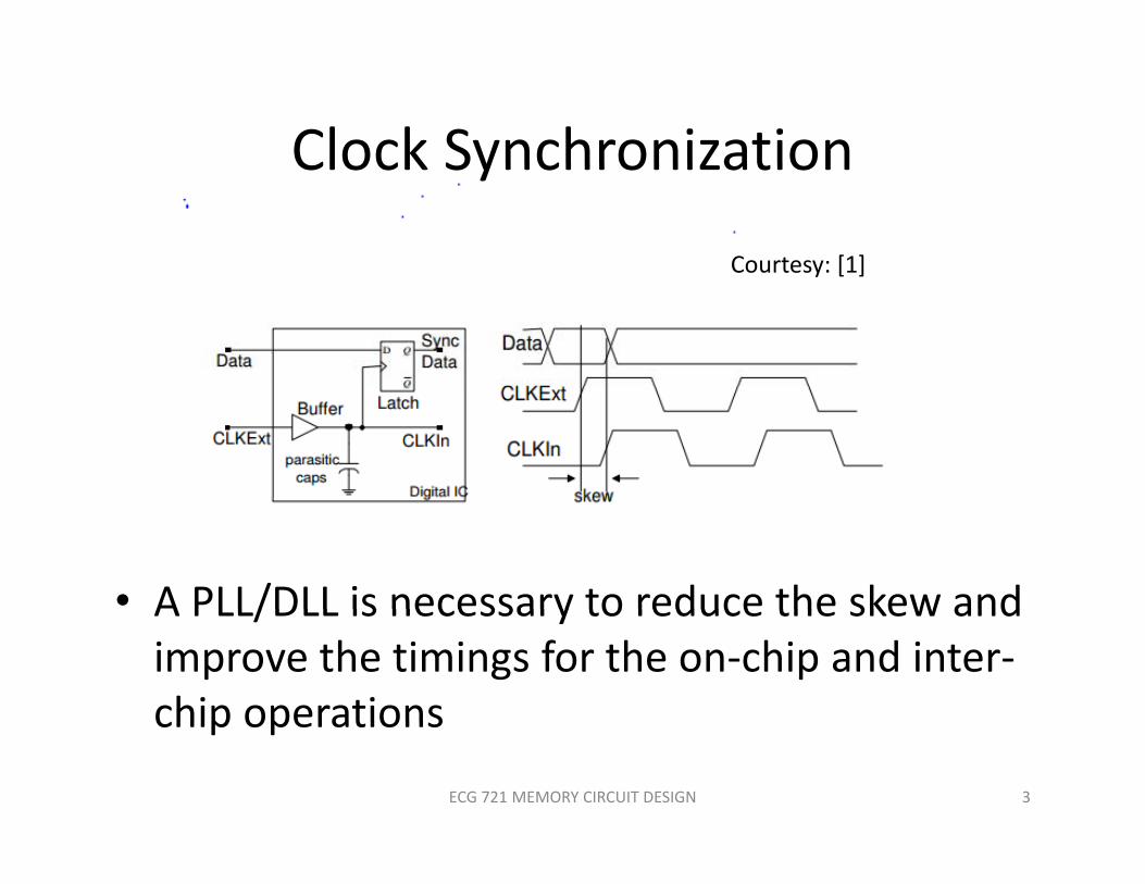
Clock SynchronizationClock Synchronization
Courtesy: [1]y [ ]
• A PLL/DLL is necessary to reduce the skew andA PLL/DLL is necessary to reduce the skew and improve the timings for the on‐chip and inter‐chip operationschip operations
3ECG 721 MEMORY CIRCUIT DESIGN
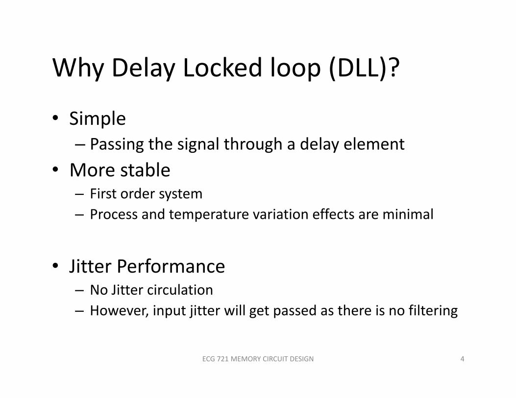
Why Delay Locked loop (DLL)?Why Delay Locked loop (DLL)?
• SimpleSimple– Passing the signal through a delay element
• More stableMore stable – First order system– Process and temperature variation effects are minimal
• Jitter Performance– No Jitter circulation– However, input jitter will get passed as there is no filtering
4ECG 721 MEMORY CIRCUIT DESIGN

Delay locked loop (DLL)Delay locked loop (DLL)
Fig 1. Delay Locked loop Block diagram [2]
5ECG 721 MEMORY CIRCUIT DESIGN
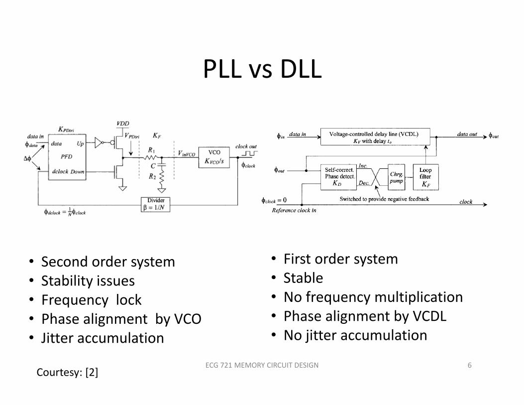
PLL vs DLLPLL vs DLL
• Second order system• Stability issues
• First order system• Stable• Stability issues
• Frequency lock• Phase alignment by VCO
Stable• No frequency multiplication• Phase alignment by VCDLN ji l i• Jitter accumulation • No jitter accumulation
6ECG 721 MEMORY CIRCUIT DESIGNCourtesy: [2]
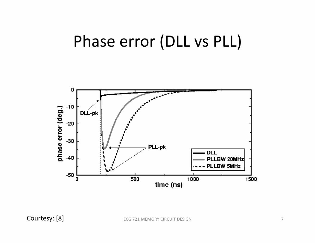
Phase error (DLL vs PLL)Phase error (DLL vs PLL)
7ECG 721 MEMORY CIRCUIT DESIGNCourtesy: [8]
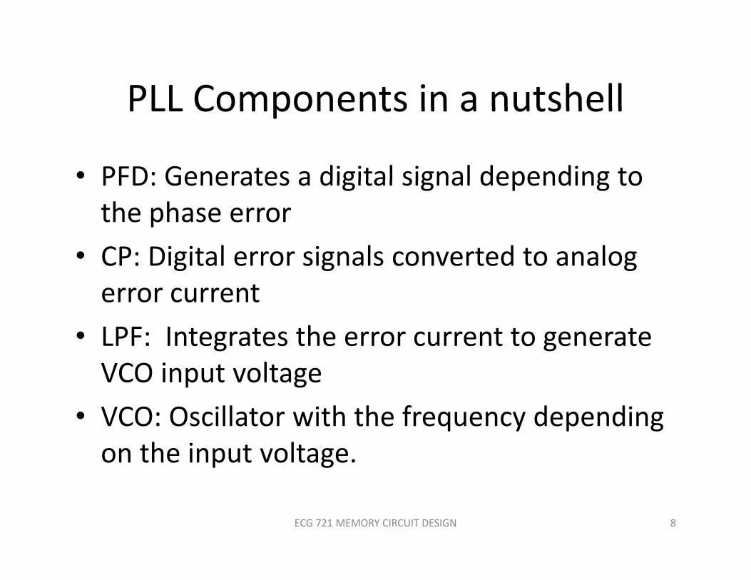
PLL Components in a nutshellPLL Components in a nutshell
• PFD: Generates a digital signal depending toPFD: Generates a digital signal depending to the phase error
• CP: Digital error signals converted to analog• CP: Digital error signals converted to analog error currentLPF I h• LPF: Integrates the error current to generate VCO input voltage
• VCO: Oscillator with the frequency depending on the input voltage.
8ECG 721 MEMORY CIRCUIT DESIGN
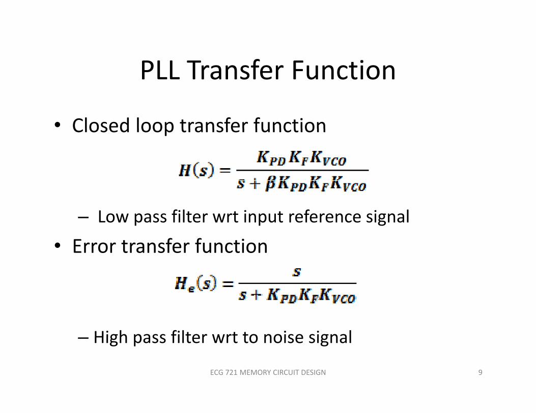
PLL Transfer FunctionPLL Transfer Function
• Closed loop transfer functionClosed loop transfer function
– Low pass filter wrt input reference signal
• Error transfer function
High pass filter wrt to noise signal– High pass filter wrt to noise signal
9ECG 721 MEMORY CIRCUIT DESIGN

Second order PLLSecond order PLL
• Reduced second order transfer function
• Where– w is the natural frequencywn is the natural frequency– Zeta is the damping factor
• Underdamped: Damping factor < 1 p p g• Critically damped: Damping factor = 1• Overdamped: Damping factor > 1
10ECG 721 MEMORY CIRCUIT DESIGN

Damping factor and natural frequencyp g q y
• wn is the frequency at which the system oscillates at zero damping• Set by the resistors and capacitors of the loop filter• Set by the resistors and capacitors of the loop filter• PLL can be stable or unstable depending on the damping factordamping factor• Stability effects phase error (Jitter) and settling time
11ECG 721 MEMORY CIRCUIT DESIGN
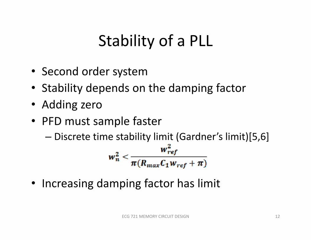
Stability of a PLLStability of a PLL
• Second order systemSecond order system• Stability depends on the damping factor• Adding zero• Adding zero• PFD must sample faster
Discrete time stability limit (Gardner’s limit)[5 6]– Discrete time stability limit (Gardner’s limit)[5,6]
• Increasing damping factor has limit
12ECG 721 MEMORY CIRCUIT DESIGN

Transfer function vs Damping factorTransfer function vs Damping factor
• Gain overshoot at low damping factorGain overshoot at low damping factor– Errors will re‐circulated and amplified
• Flattens out as damping factor increases• Flattens out as damping factor increases
• Gain overshoot at the higher damping factor due to stability limit (Gardner limit)
• Good Compromise – damping factor = 1
13ECG 721 MEMORY CIRCUIT DESIGN

Transfer function vs Damping factorTransfer function vs Damping factor
14ECG 721 MEMORY CIRCUIT DESIGNCourtesy: [3]
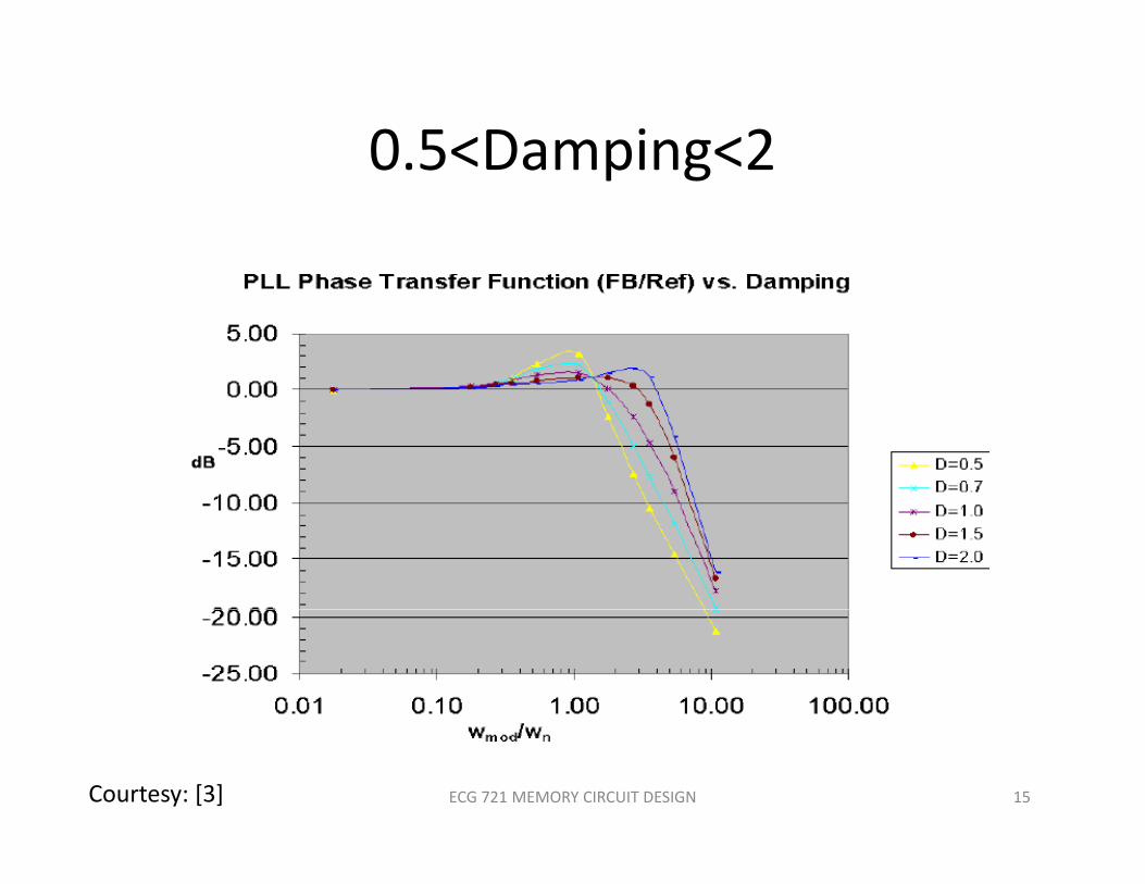
0.5<Damping<20.5<Damping<2
15ECG 721 MEMORY CIRCUIT DESIGNCourtesy: [3]

Phase response Vs dampingPhase response Vs damping
• Transient simulation for phase stepTransient simulation for phase step
• Overshoot and ringing for under‐damped• Overshoot and ringing for under‐damped systems
• Minimal overshoot and ringing for critically• Minimal overshoot and ringing for critically damped
• Overshoot and fast ringing for over‐damped• Overshoot and fast ringing for over‐damped systems– Due to Gardner’s limitDue to Gardner s limit
16ECG 721 MEMORY CIRCUIT DESIGN
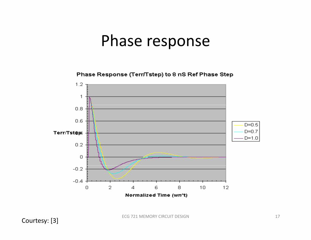
Phase responsePhase response
17ECG 721 MEMORY CIRCUIT DESIGNCourtesy: [3]

Phase responsePhase response
18ECG 721 MEMORY CIRCUIT DESIGNCourtesy: [3]
Other key parameters of PLLOther key parameters of PLL
• Hold range: Frequency range that the PLL can g q y gtrack without losing lock
• Lock range: Frequency range at which the loop recapture the lock within one cyclerecapture the lock within one cycle
• Lock time: Time taken for PLL to lock during the lock in processlock in process
• Pull in range: Frequency range in which the loop can acquire a lock
• Pull in time: Time taken for PLL to lock during the pull in process
19ECG 721 MEMORY CIRCUIT DESIGN
Noise in PLLNoise in PLL
• Types of noiseTypes of noise– Flicker noise: Caused by silicon interface traps– Thermal noise: Caused by random Brownian ymotion of carriers in a resistive medium
• Noise in PLL components– Charge Pump: Flicker and thermal– Loop Filter: Mostly thermal– VCO: Mostly thermal– VCO Bias: Flicker and thermal
20ECG 721 MEMORY CIRCUIT DESIGN
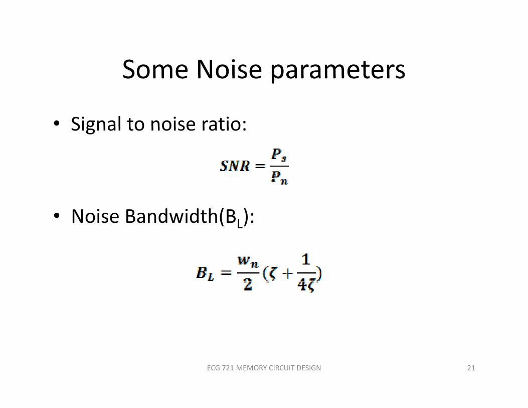
Some Noise parametersSome Noise parameters
• Signal to noise ratio:Signal to noise ratio:
• Noise Bandwidth(BL):
21ECG 721 MEMORY CIRCUIT DESIGN
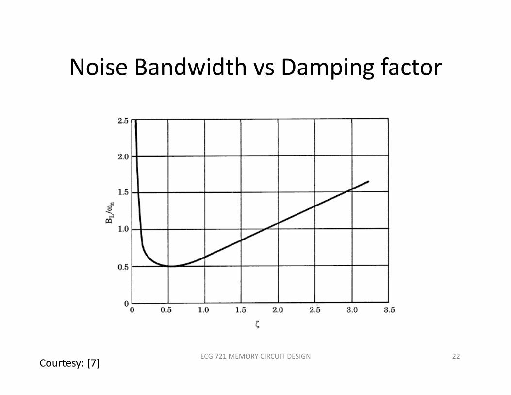
Noise Bandwidth vs Damping factorNoise Bandwidth vs Damping factor
22ECG 721 MEMORY CIRCUIT DESIGNCourtesy: [7]
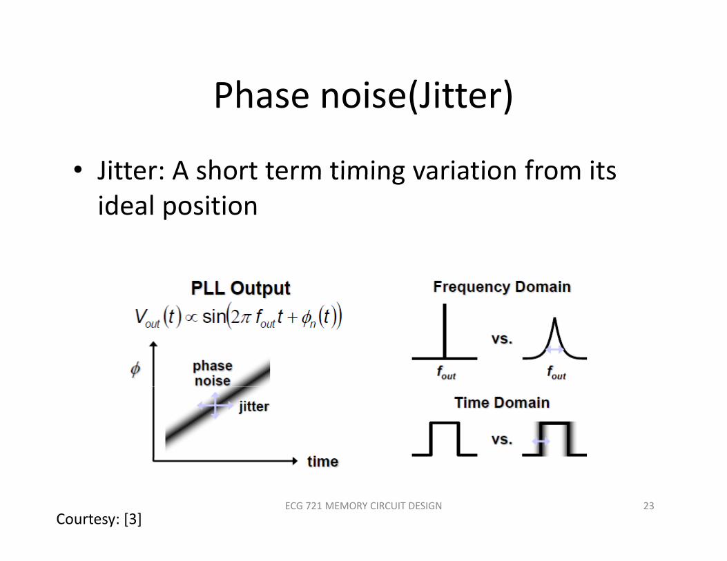
Phase noise(Jitter)Phase noise(Jitter)
• Jitter: A short term timing variation from itsJitter: A short term timing variation from its ideal position
23ECG 721 MEMORY CIRCUIT DESIGNCourtesy: [3]
Jitter measurementJitter measurement
• Phase Jitter– Deviation of VCO output edges from ideal placement in time
• Period Jitter• Period Jitter– Deviation of VCO period from the ideal period– Derivative of phase Jitter wrt timep
• Cycle to cycle Jitter– Change in VCO period from cycle N to cycle N+1
• TIE(Time interval error)– Time difference between total of N consecutive actual VCO cycle and N ideal cyclesVCO cycle and N ideal cycles
24ECG 721 MEMORY CIRCUIT DESIGN
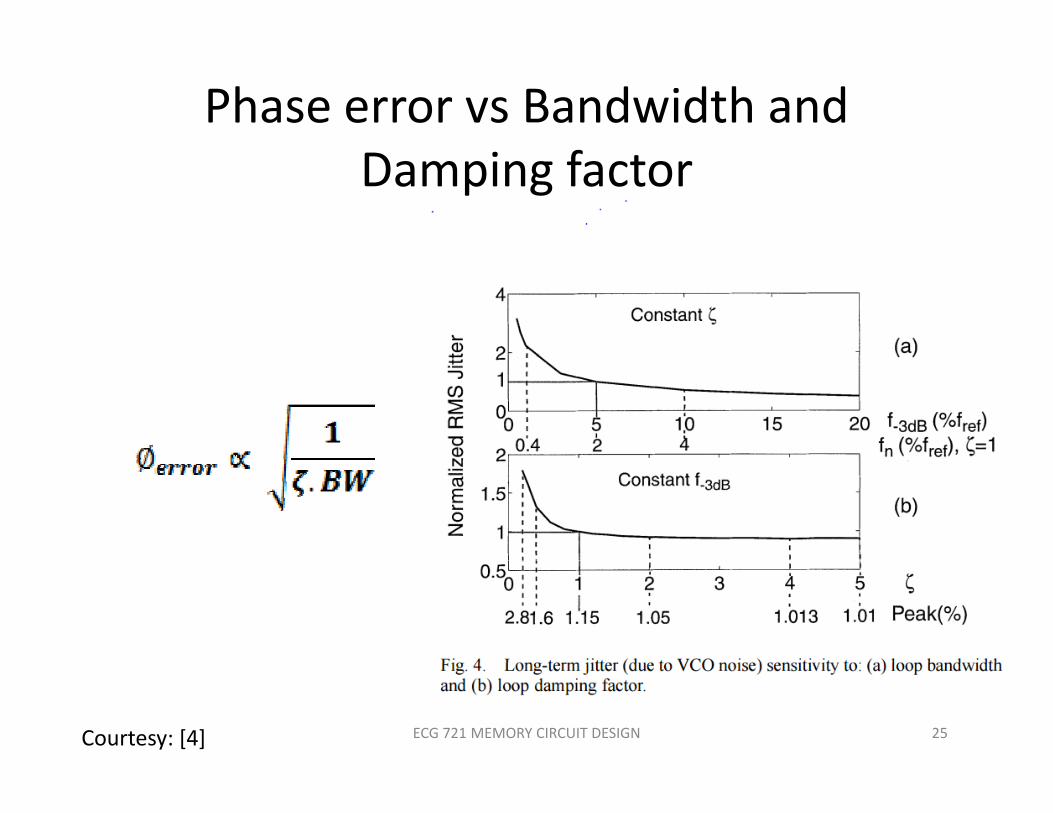
Phase error vs Bandwidth and fDamping factor
25ECG 721 MEMORY CIRCUIT DESIGNCourtesy: [4]

Jitter reductionJitter reduction
• Increase frequencyIncrease frequency• Increase the gate area of the transistors
i h di i i• Increasing the power dissipation• Choosing number of stages at VCO
–More stages can reduce noise
• Differential delay buffer as a stage in VCOy g• Self biased techniques to track process and temperature variationtemperature variation
26ECG 721 MEMORY CIRCUIT DESIGN

ConclusionConclusion
• Major advantages of PLLj g– Input noise filtered– Can generate frequenciesC d d PLL i d f DLL i• Can we use overdamped PLL instead of DLL in SDRAM?– Yes. But not recommendedYes. But not recommended
• Disadvantages– Stability– Jitter accumulation– Higher pull in timeMust tract frequency input– Must tract frequency input
27ECG 721 MEMORY CIRCUIT DESIGN
ReferenceReference[1] F.Lin, “Research and Design of Low Jitter, Wide Locking‐Range All‐Digital
h k d d l k d ”Phase‐Locked and Delay‐Locked Loops” 2000.[2] J. Baker, CMOS: Circuit Design, Layout and Simulation, Third Edition. Wiley‐
IEEE, ISBN 978‐0‐470‐22941‐5, 2008.[3] D i Fi h tt “P ti l Ph L k d L D i ” ISSCC 2007[3] Dennis Fischette “Practical Phase‐Locked Loop Design” ISSCC 2007
Tutorial.[4] M. Mansuri, Chih Kong Ken, “Jitter optimization based on phase‐locked
loop design parameters” JSSC‐2002 Vol 37 Issue 11loop design parameters JSSC 2002, Vol 37, Issue 11[5] F M Gardner, “Charge pump Phase locked loop”, IEEE transactions on
Communications, Vol 28, No:11, Nov 1980[6] F M Gardner, “Phase lock techniques” Third Edition. Wiley‐IEEE.[6] F M Gardner, Phase lock techniques Third Edition. Wiley IEEE.[7] Roland Best, “ Phase locked loops design simulation and applications ”
Mcgraw hill, Sixth edition[8] Changsik Yoo, “Delay‐Locked Loop‐Design Examples, Design Issues/Tips” [ ] g , y p g p , g / p
28ECG 721 MEMORY CIRCUIT DESIGN

Thank you!y
29ECG 721 MEMORY CIRCUIT DESIGN