University of Tehran 1 Interface Design Memory Modules Omid Fatemi ([email protected])
105
Transcript of University of Tehran 1 Interface Design Memory Modules Omid Fatemi ([email protected])

University of Tehran 2
Outline
• Memory variations
• The memory cell

University of Tehran 3
Processor Timing Diagramfor any memory read machine cycle
IOR
IOW
MEMR
MEMW
___
____
_____
______
AddressBus
Data Bus
T1 T2 T3
CLOCK
memory address
datain

University of Tehran 4
Processor Timing Diagramfor any memory write machine cycle
IOR
IOW
MEMR
MEMW
___
____
_____
______
AddressBus
Data Bus
T1 T2 T3
CLOCK
memory address
data out

University of Tehran 5
Memory Terms
• Capacity – Kbit, Mbit, Gbit
• Organization– Address lines
– Data lines
• Speed / Timing– Access time
• Write ability– ROM
– RAM
University of Tehran 6
ROM Variations
• Mask Rom
• PROM – OTP
• EPROM – UV_EPROM
• EEPROM
• Flash memory
University of Tehran 7
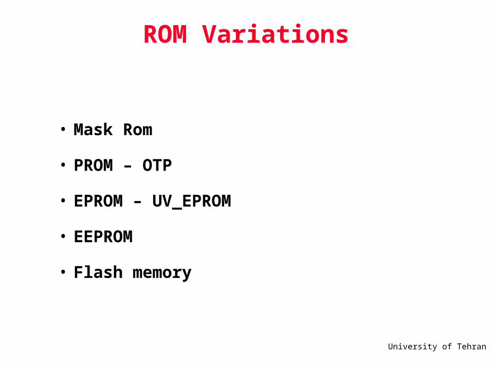
RAM Variations
• SRAM
• DRAM
• NV-RAM
– SRAM – CMOS
– Internal lithium battery
– Control circuitry to monitor Vcc
University of Tehran 8
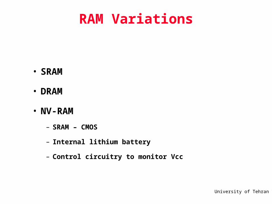
Memories in General
• Computers have mostly RAM
• ROM (or equivalent) needed to boot
• ROM is in same class as Programmable Logic
Devices (PLDs), in which are also FPGAs
– Lots of memories in these devices

University of Tehran 9
Simple View of RAM
• Of some word size n
• Some capacity 2k
• k bits of address line
• Maybe have read line
• Have a write line
• Have a CS (chip select)
University of Tehran 10
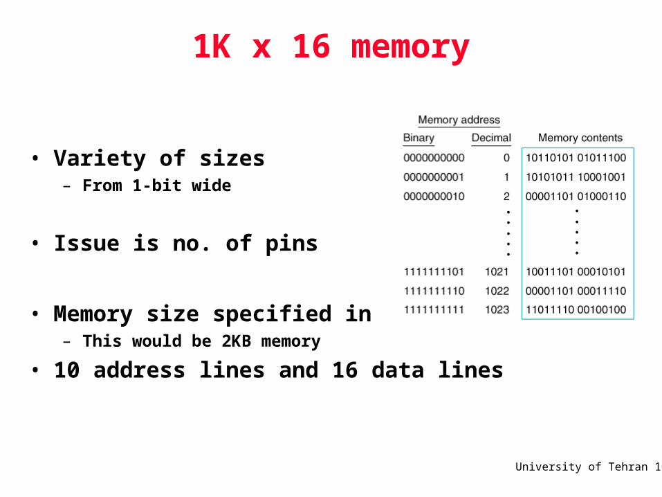
1K x 16 memory
• Variety of sizes– From 1-bit wide
• Issue is no. of pins
• Memory size specified in bytes– This would be 2KB memory
• 10 address lines and 16 data lines
University of Tehran 11
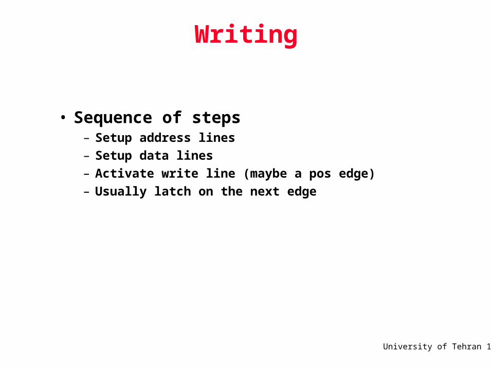
Writing
• Sequence of steps– Setup address lines
– Setup data lines
– Activate write line (maybe a pos edge)
– Usually latch on the next edge

University of Tehran 12
Reading
• Steps– Setup address lines
– Activate read line
– Data available after specified amt of time

University of Tehran 13
Chip Select
• Usually a line to enable the chip

University of Tehran 14
Writing

University of Tehran 15
Reading

University of Tehran 16
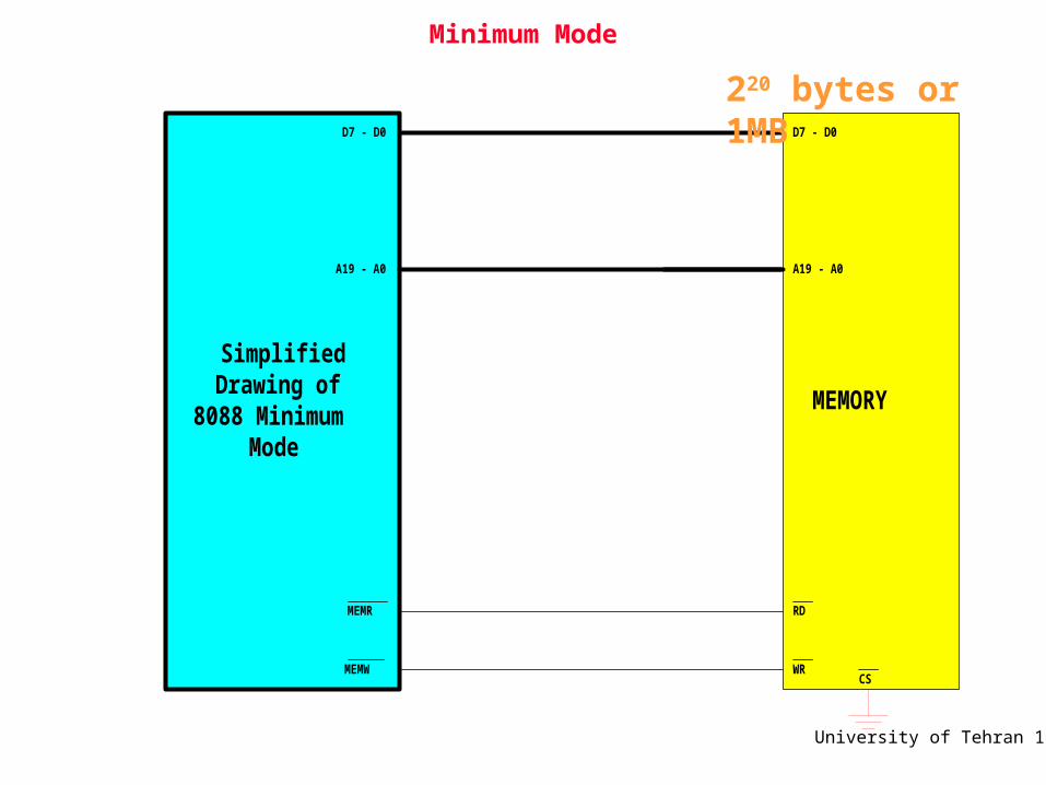
Minimum Mode
MEMORY
D7 - D0 Q7 - Q0
OE
LE 74LS373
D7 - D0 Q7 - Q0
OE
LE 74LS3738088
AD7 - AD0
A15 - A8
A19/S6 - A16/S3
DEN
DT / R
IO / M
RD
WR
ALE
D7 - D4 Q7 - Q4
OE
LE 74LS373
D3 - D0 Q3 - Q0
GND
GND
GND
D7 - D0A7 - A0 B7 - B0
E
DIR 74LS245
A7 - A0
A15 - A8
A19 - A16
RD
WR

University of Tehran 17
Minimum Mode
MEMORY
D7 - D0
A19 - A0
RD
WR
SimplifiedDrawing of
8088 MinimumMode
D7 - D0
A19 - A0
MEMR
MEMW
When Memory is selected?
University of Tehran 18
Minimum Mode
MEMORY
D7 - D0
A19 - A0
RD
WR
SimplifiedDrawing of
8088 MinimumMode
D7 - D0
A19 - A0
MEMR
MEMWCS
220 bytes or 1MB

University of Tehran 19
What are the memory locations of a 1MB (220 bytes) Memory?
A19 to A0
(HEX)
AAAA
1111
9876
AAAA
1111
5432
AAAA
1198
1000
AAAA
7654
AAAA
3210
00000 0000 0000 0000 0000 0000
FFFFF 1111 1111 1111 1111 1111
Example: 34FD0 0011 0100 11111 1101 0000

University of Tehran 20
Interfacing a 1MB Memory to the 8088 Microprocessor
2300000
00001
10000
10001
10002
10003
10004
10005
10006
10007
10008
95
::
45
98
27
39
42
88
07
F4
8A
::
20020
20021
20022
20023
FFFFD
FFFFE
FFFFF
29
12
7D
13
19
25
36
::
::
::
::
A19
A0
:
D7
D0
:
RD
WR
A19
A0
:
D7
D0
:
MEMR
MEMW
XXXX
BP
ES
DS
SS
CX
BX
AX
XXXX
XXXX
XXXX
2000
0000
0023
3F1C
FCA1
SP
DX
XXXX
CS
SI
XXXX
XXXXIP
XXXXDI
CS

University of Tehran 21
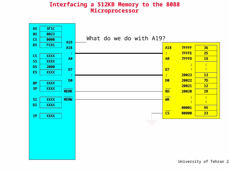
Instead of Interfacing 1MB, what will happen if you interface a 512KB Memory?

University of Tehran 22
What are the memory locations of a 512KB (219 bytes) Memory?
A18 to A0
(HEX)
AAAA
1111
9876
AAAA
1111
5432
AAAA
1198
1000
AAAA
7654
AAAA
3210
00000 0000 0000 0000 0000 0000
7FFFF 0111 1111 1111 1111 1111
University of Tehran 23
Interfacing a 512KB Memory to the 8088 Microprocessor
A18
A0
:
D7
D0
:
MEMR
MEMWXXXX
BP
ES
DS
SS
CX
BX
AX
XXXX
XXXX
XXXX
2000
0000
0023
3F1C
FCA1
SP
DX
XXXX
CS
SI
XXXX
XXXXIP
XXXXDI
2300000
00001 95
::
20020
20021
20022
20023
7FFFD
7FFFE
7FFFF
29
12
7D
13
19
25
36
::
::
::
A18
A0
:
D7
D0
:
RD
WR
CS
A19What do we do with A19?

University of Tehran 24
What if you want to read physical address A0023?
A18
A0
:
D7
D0
:
MEMR
MEMWXXXX
BP
ES
DS
SS
CX
BX
AX
XXXX
XXXX
XXXX
A000
0000
0023
3F1C
FCA1
SP
DX
XXXX
CS
SI
XXXX
XXXXIP
XXXXDI
2300000
00001 95
::
20020
20021
20022
20023
7FFFD
7FFFE
7FFFF
29
12
7D
13
19
25
36
::
::
::
A18
A0
:
D7
D0
:
RD
WR
CS
A19

University of Tehran 25
What if you want to read physical address A0023?
A19 to A0
(HEX)
AAAA
1111
9876
AAAA
1111
5432
AAAA
1198
1000
AAAA
7654
AAAA
3210
A0023 1010 0000 0000 0010 0011
A19 is not connected to the memory so even if the 8088 microprocessor outputs a logic “1”, the memory cannot “see” this.
University of Tehran 26
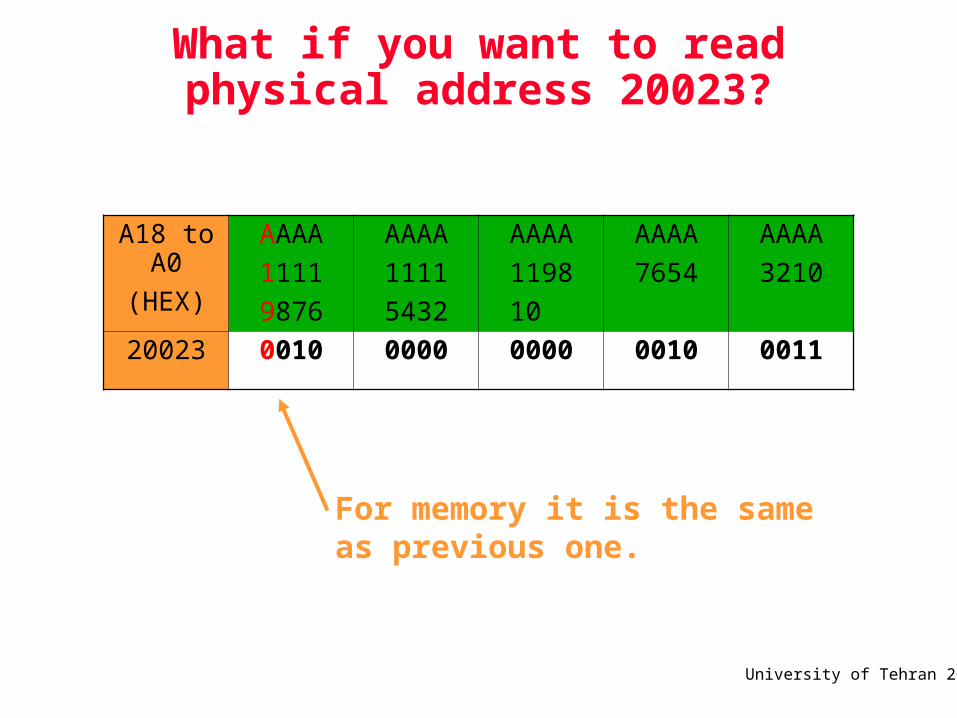
What if you want to read physical address 20023?
A18 to A0
(HEX)
AAAA
1111
9876
AAAA
1111
5432
AAAA
1198
1000
AAAA
7654
AAAA
3210
20023 0010 0000 0000 0010 0011
For memory it is the same as previous one.

University of Tehran 27
Interfacing two 512KB Memory to the 8088 Microprocessor
A18
A0
:
D7
D0
:
MEMR
MEMW
XXXX
BP
ES
DS
SS
CX
BX
AX
XXXX
XXXX
XXXX
2000
0000
0023
3F1C
FCA1
SP
DX
XXXX
CS
SI
XXXX
XXXXIP
XXXXDI
A19
2300000
00001 95
:
20020
20021
20022
20023
7FFFD
7FFFE
7FFFF
29
12
7D
13
19
25
36
:
:
:
A18
A0
:
D7
D0
:
RD
WR
CS
9700000
00001 D4
:
20020
20021
20022
20023
7FFFD
7FFFE
7FFFF
A3
92
45
33
2C
98
12
:
:
:
A18
A0
:
D7
D0
:
RD
WR
CS

University of Tehran 28
Interfacing two 512KB Memory to the 8088 Microprocessor
• Problem: Bus Conflict. The two memory chips will provide data at the same time when microprocessor performs a memory read.
• Solution: Use address line A19 as an “arbiter”. If A19 outputs a logic “1” the upper memory is enabled (and the lower memory is disabled) and vice-versa.

University of Tehran 29
Interfacing two 512KB Memory to the 8088 Microprocessor
A18
A0
:
D7
D0
:
MEMR
MEMW
XXXX
BP
ES
DS
SS
CX
BX
AX
XXXX
XXXX
XXXX
2000
0000
0023
3F1C
FCA1
SP
DX
XXXX
CS
SI
XXXX
XXXXIP
XXXXDI
A19
2300000
00001 95
:
20020
20021
20022
20023
7FFFD
7FFFE
7FFFF
29
12
7D
13
19
25
36
:
:
:
A18
A0
:
D7
D0
:
RD
WR
CS
9700000
00001 D4
:
20020
20021
20022
20023
7FFFD
7FFFE
7FFFF
A3
92
45
33
2C
98
12
:
:
:
A18
A0
:
D7
D0
:
RD
WR
CS

University of Tehran 30
What are the memory locations of two consecutive 512KB (219 bytes) Memory?
A19 to A0
(HEX)
AAAA
1111
9876
AAAA
1111
5432
AAAA
1198
1000
AAAA
7654
AAAA
3210
00000 0000 0000 0000 0000 0000
7FFFF 0111 1111 1111 1111 1111
80000 1000 0000 0000 0000 0000
FFFFF 1111 1111 1111 1111 1111

University of Tehran 31
A18
A0
:
D7
D0
:
MEMR
MEMW
XXXX
BP
ES
DS
SS
CX
BX
AX
XXXX
XXXX
XXXX
2000
0000
0023
3F1C
FCA1
SP
DX
XXXX
CS
SI
XXXX
XXXXIP
XXXXDI
A19
2300000
00001 95
:
20020
20021
20022
20023
7FFFD
7FFFE
7FFFF
29
12
7D
13
19
25
36
:
:
:
A18
A0
:
D7
D0
:
RD
WR
CS
9700000
00001 D4
:
20020
20021
20022
20023
7FFFD
7FFFE
7FFFF
A3
92
45
33
2C
98
12
:
:
:
A18
A0
:
D7
D0
:
RD
WR
CS
Interfacing two 512KB Memory to the 8088 Microprocessor
When the P outputs an address between 80000 to FFFFF, this memory is selected
When the P outputs an address between 00000 to 7FFFF, this memory is selected

University of Tehran 32
Interfacing two 512KB Memory to the 8088 Microprocessor
A18
A0
:
D7
D0
:
MEMR
MEMW
XXXX
BP
ES
DS
SS
CX
BX
AX
XXXX
XXXX
XXXX
2000
0000
0023
3F1C
FCA1
SP
DX
XXXX
CS
SI
XXXX
XXXXIP
XXXXDI
A19
2300000
00001 95
:
20020
20021
20022
20023
7FFFD
7FFFE
7FFFF
29
12
7D
13
19
25
36
:
:
:
A18
A0
:
D7
D0
:
RD
WR
CS
9700000
00001 D4
:
20020
20021
20022
20023
7FFFD
7FFFE
7FFFF
A3
92
45
33
2C
98
12
:
:
:
A18
A0
:
D7
D0
:
RD
WR
CS

University of Tehran 33
Interfacing two 512KB Memory to the 8088 Microprocessor
A18
A0
:
D7
D0
:
MEMR
MEMW
XXXX
BP
ES
DS
SS
CX
BX
AX
XXXX
XXXX
XXXX
2000
0000
0023
3F1C
FCA1
SP
DX
XXXX
CS
SI
XXXX
XXXXIP
XXXXDI
A19
2300000
00001 95
:
20020
20021
20022
20023
7FFFD
7FFFE
7FFFF
29
12
7D
13
19
25
36
:
:
:
A18
A0
:
D7
D0
:
RD
WR
CS
9700000
00001 D4
:
20020
20021
20022
20023
7FFFD
7FFFE
7FFFF
A3
92
45
33
2C
98
12
:
:
:
A18
A0
:
D7
D0
:
RD
WR
CS
A18
A0
:
D7
D0
:
RD
WR
A19

University of Tehran 34
A18
A0
:
D7
D0
:
MEMR
MEMW
XXXX
BP
ES
DS
SS
CX
BX
AX
XXXX
XXXX
XXXX
2000
0000
0023
3F1C
FCA1
SP
DX
XXXX
CS
SI
XXXX
XXXXIP
XXXXDI
A19
2300000
00001 95
:
20020
20021
20022
20023
7FFFD
7FFFE
7FFFF
29
12
7D
13
19
25
36
:
:
:
A18
A0
:
D7
D0
:
RD
WR
CS
9700000
00001 D4
:
20020
20021
20022
20023
7FFFD
7FFFE
7FFFF
A3
92
45
33
2C
98
12
:
:
:
A18
A0
:
D7
D0
:
RD
WR
CS
What if we remove the lower memory?

University of Tehran 35
What if we remove the lower memory?
A18
A0
:
D7
D0
:
MEMR
MEMW
XXXX
BP
ES
DS
SS
CX
BX
AX
XXXX
XXXX
XXXX
2000
0000
0023
3F1C
FCA1
SP
DX
XXXX
CS
SI
XXXX
XXXXIP
XXXXDI
A19
2300000
00001 95
:
20020
20021
20022
20023
7FFFD
7FFFE
7FFFF
29
12
7D
13
19
25
36
:
:
:
A18
A0
:
D7
D0
:
RD
WR
CSWhen the P outputs an address between 80000 to FFFFF, this memory is selected
When the P outputs an address between 00000 to 7FFFF, no memory chip is selected !

University of Tehran 36
Full and Partial Decoding
• Full Decoding– When all of the “useful” address lines are connected the
memory/device to perform selection
• Partial Decoding– When some of the “useful” address lines are connected
the memory/device to perform selection
– Using this type of decoding results into roll-over addresses

University of Tehran 37
Full Decoding
A18
A0
:
D7
D0
:
MEMR
MEMW
XXXX
BP
ES
DS
SS
CX
BX
AX
XXXX
XXXX
XXXX
2000
0000
0023
3F1C
FCA1
SP
DX
XXXX
CS
SI
XXXX
XXXXIP
XXXXDI
A19
2300000
00001 95
:
20020
20021
20022
20023
7FFFD
7FFFE
7FFFF
29
12
7D
13
19
25
36
:
:
:
A18
A0
:
D7
D0
:
RD
WR
CS
University of Tehran 38
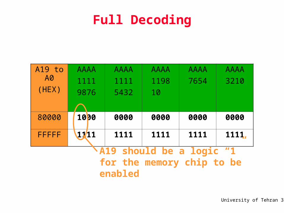
Full Decoding
A19 to A0
(HEX)
AAAA
1111
9876
AAAA
1111
5432
AAAA
1198
1000
AAAA
7654
AAAA
3210
80000 1000 0000 0000 0000 0000
FFFFF 1111 1111 1111 1111 1111
A19 should be a logic “1” for the memory chip to be enabled

University of Tehran 39
Full Decoding
A19 to A0
(HEX)
AAAA
1111
9876
AAAA
1111
5432
AAAA
1198
1000
AAAA
7654
AAAA
3210
00000 0000 0000 0000 0000 0000
7FFFF 0111 1111 1111 1111 1111
Therefore if the microprocessor outputs an address between 00000 to 7FFFF, whose A19 is a logic “0”, the memory chip will not be selected

University of Tehran 40
Partial Decoding
A18
A0
:
D7
D0
:
MEMR
MEMWXXXX
BP
ES
DS
SS
CX
BX
AX
XXXX
XXXX
XXXX
2000
0000
0023
3F1C
FCA1
SP
DX
XXXX
CS
SI
XXXX
XXXXIP
XXXXDI
2300000
00001 95
::
20020
20021
20022
20023
7FFFD
7FFFE
7FFFF
29
12
7D
13
19
25
36
::
::
::
A18
A0
:
D7
D0
:
RD
WR
CS
A19

University of Tehran 41
Partial Decoding
A19 to A0
(HEX)
AAAA
1111
9876
AAAA
1111
5432
AAAA
1198
1000
AAAA
7654
AAAA
3210
00000 0000 0000 0000 0000 0000
7FFFF 0111 1111 1111 1111 1111
80000 1000 0000 0000 0000 0000
FFFFF 1111 1111 1111 1111 1111
The value of A19 is INSIGNIFICANT to the memory chip, therefore A19 has no bearing whether the memory chip will be enabled or not

University of Tehran 42
Partial Decoding
A19 to A0
(HEX)
AAAA
1111
9876
AAAA
1111
5432
AAAA
1198
1000
AAAA
7654
AAAA
3210
00000 0000 0000 0000 0000 0000
7FFFF 0111 1111 1111 1111 1111
80000 1000 0000 0000 0000 0000
FFFFF 1111 1111 1111 1111 1111
ACTUAL ADDRESS

University of Tehran 43
Partial Decoding
A19 to A0
(HEX)
AAAA
1111
9876
AAAA
1111
5432
AAAA
1198
1000
AAAA
7654
AAAA
3210
00000 0000 0000 0000 0000 0000
7FFFF 0111 1111 1111 1111 1111
80000 1000 0000 0000 0000 0000
FFFFF 1111 1111 1111 1111 1111
ACTUAL ADDRESS

University of Tehran 44
Interfacing two 512K Memory Chips to the 8088 Microprocessor
8088Minimum
Mode
A18
A0
:
D7
D0
:
MEMR
MEMW
A19
512KB#2
A18
A0
:
D7
D0
:
RD
WR
CS
512KB#1
A18
A0
:
D7
D0
:
RD
WR
CS

University of Tehran 45
Interfacing one 512K Memory Chips to the 8088 Microprocessor
8088Minimum
Mode
A18
A0
:
D7
D0
:
MEMR
MEMW
A19
512KB
A18
A0
:
D7
D0
:
RD
WR
CS

University of Tehran 46
Interfacing one 512K Memory Chips to the 8088 Microprocessor (version 2)
8088Minimum
Mode
A18
A0
:
D7
D0
:
MEMR
MEMW
A19
512KB
A18
A0
:
D7
D0
:
RD
WR
CS
University of Tehran 47
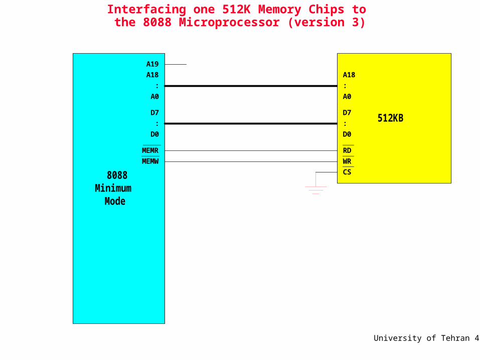
Interfacing one 512K Memory Chips to the 8088 Microprocessor (version 3)
8088Minimum
Mode
A18
A0
:
D7
D0
:
MEMR
MEMW
A19
512KB
A18
A0
:
D7
D0
:
RD
WR
CS

University of Tehran 48
Interfacing four 256K Memory Chips to the 8088 Microprocessor
8088Minimum
Mode
A17
A0:
D7
D0:
MEMRMEMW
A18
256KB#3
A17
A0:
D7
D0:
RDWR
CS
A19
256KB#2
A17
A0:
D7
D0:
RDWR
CS
256KB#1
A17
A0:
D7
D0:
RDWR
CS
256KB#4
A17
A0:
D7
D0:
RDWR
CS

University of Tehran 49
Interfacing four 256K Memory Chips to the 8088 Microprocessor
8088Minimum
Mode
A17
A0:
D7
D0:
MEMRMEMW
A18
256KB#3
A17
A0:
D7
D0:
RDWR
CS
A19
256KB#2
A17
A0:
D7
D0:
RDWR
CS
256KB#1
A17
A0:
D7
D0:
RDWR
CS
256KB#4
A17
A0:
D7
D0:
RDWR
CS

University of Tehran 50
Interfacing four 256K Memory Chips to the 8088 Microprocessor
8088Minimum
Mode
A17
A0:
D7
D0:
MEMRMEMW
A18
256KB#3
A17
A0:
D7
D0:
RDWR
CS
A19
256KB#2
A17
A0:
D7
D0:
RDWR
CS
256KB#1
A17
A0:
D7
D0:
RDWR
CS
256KB#4
A17
A0:
D7
D0:
RDWR
CS

University of Tehran 51
Interfacing four 256K Memory Chips to the 8088 Microprocessor
8088Minimum
Mode
A17
A0:
D7
D0:
MEMRMEMW
A18
256KB#3
A17
A0:
D7
D0:
RDWR
CS
A19
256KB#2
A17
A0:
D7
D0:
RDWR
CS
256KB#1
A17
A0:
D7
D0:
RDWR
CS
256KB#4
A17
A0:
D7
D0:
RDWR
CSI1I0
O3
O2
O1
O0

University of Tehran 52
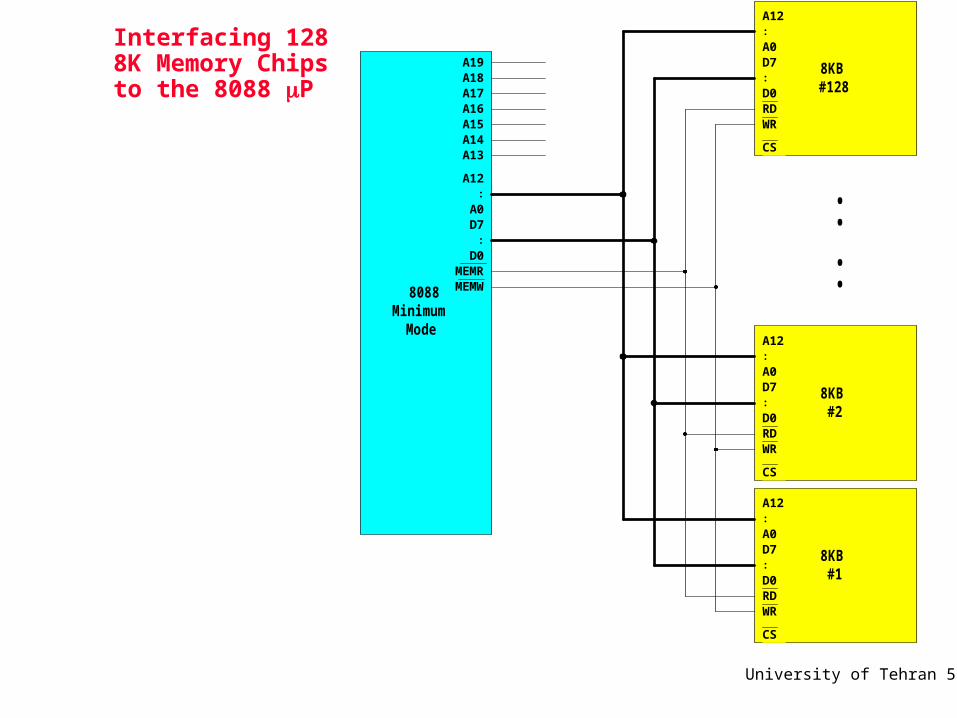
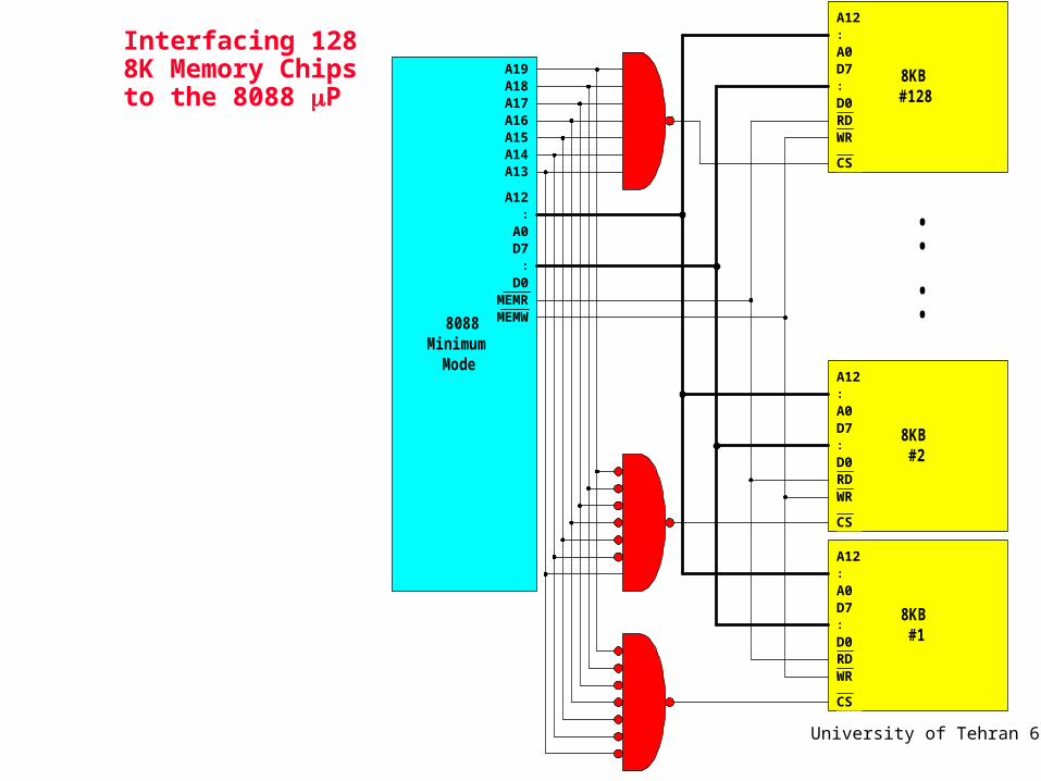
Interfacing several 8K Memory Chips to the 8088 P
8088Minimum
Mode
A12
A0:
D7
D0:
MEMRMEMW
A13A14
8KB#2
A12
A0:
D7
D0:
RDWR
CS
8KB#1
A12
A0:
D7
D0:
RDWR
CS
8KB#?
A12
A0:
D7
D0:
RDWR
CS
A15A16A17A18A19
::
University of Tehran 53
8088Minimum
Mode
A12
A0:
D7
D0:
MEMRMEMW
A13A14
8KB#2
A12
A0:
D7
D0:
RDWR
CS
8KB#1
A12
A0:
D7
D0:
RDWR
CS
8KB#128
A12
A0:
D7
D0:
RDWR
CS
A15A16A17A18A19
::
Interfacing 1288K Memory Chips to the 8088 P

University of Tehran 54
8088Minimum
Mode
A12
A0:
D7
D0:
MEMRMEMW
A13A14
8KB#2
A12
A0:
D7
D0:
RDWR
CS
8KB#1
A12
A0:
D7
D0:
RDWR
CS
8KB#128
A12
A0:
D7
D0:
RDWR
CS
A15A16A17A18A19
::
Interfacing 1288K Memory Chips to the 8088 P

University of Tehran 55
Memory chip#__ is mapped to:
A19 to A0
(HEX)
AAAA
1111
9876
AAAA
1111
5432
AAAA
1198
1000
AAAA
7654
AAAA
3210
----- ---- ---- ---- ---- ----
----- ---- ---- ---- ---- ----

University of Tehran 56
Memory Chip
• 8K SRAM
• to be specific:– 8Kx8 bits SRAM
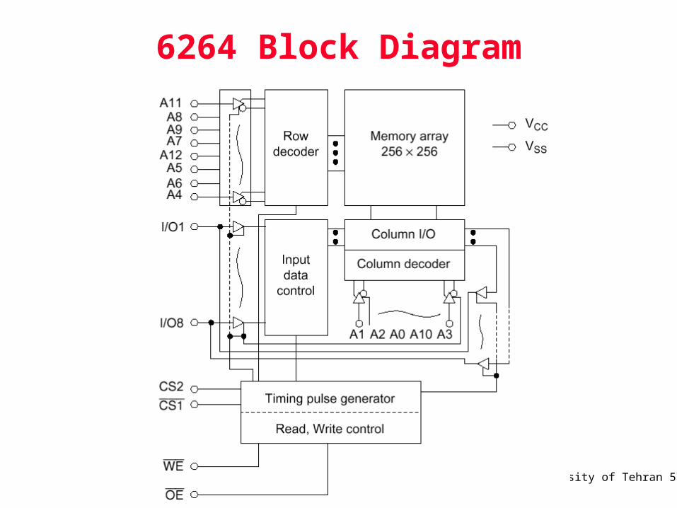
6264
A0
A1
A2
A3
A4
A5
A6
A7
A8
A9
A10
A11
A12
CS2
I/O0
I/O 1
I/O 2
I/O 3
I/O 4
I/O 5
I/O 6
I/O 7
CS1
OE
WE
University of Tehran 57
6264 Block Diagram

University of Tehran 58
6264 Function Table

University of Tehran 59
Memory Chip
• 8K EPROM
• to be specific:– 8Kx8 bits EPROM
2764
A0
A1
A2
A3
A4
A5
A6
A7
A8
A9
A10
A11
A12
VPP
Q0
Q1
Q2
Q3
Q4
Q5
Q6
Q7
C
G
P

University of Tehran 60
2764 Block Diagram
Chip enable
Output enable

University of Tehran 61
Operating Modes
University of Tehran 62
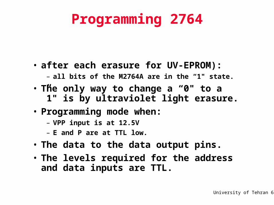
Programming 2764
• after each erasure for UV-EPROM):– all bits of the M2764A are in the “1" state.
• The only way to change a “0" to a ”1" is by ultraviolet light erasure.
• Programming mode when:– VPP input is at 12.5V
– E and P are at TTL low.
• The data to the data output pins.
• The levels required for the address and data inputs are TTL.
University of Tehran 63
8088Minimum
Mode
A12
A0:
D7
D0:
MEMRMEMW
A13A14
8KB#2
A12
A0:
D7
D0:
RDWR
CS
8KB#1
A12
A0:
D7
D0:
RDWR
CS
8KB#128
A12
A0:
D7
D0:
RDWR
CS
A15A16A17A18A19
::
Interfacing 1288K Memory Chips to the 8088 P

University of Tehran 64
When interfacing memory chips to a microprocessor, consider the following:
• TAVDV – address access time
• TRLDV – read access time
• TDVWH – memory setup time
• TWHDX – data hold time
• TWLWH – write pulse width
Refer to 8088 data manual

University of Tehran 65
HM6264B Series Read Timing Diagram
tAA, tOE

University of Tehran 66
HM6264B Series Write Timing Diagram
tDW, tDH, tWP

University of Tehran 67
Timing Requirements for 6264 SRAM
• TAVDV = tAA
• TRLDV = tOE
• TDVWH = tDW
• TWHDX = tDH
• TWLWH = tWP

University of Tehran 68
HM6264B Series Read TIMING REQUIREMENTS
HM6264B-8L HM6264B-10L Symbol Parameter Min Max Min Max
Units
tRC Read cycle time 85 100 ns
tAA Address access time 85 100 ns
tCO1 Chip select access time (CS1’) 85 100 ns
tCO2 Chip select access time (CS2’) 85 100 ns
tOE Output enable to output valid 45 50 ns
tLZ1 Chip selection to output in low-Z (CS1)
10 10 ns
tLZ2 Chip selection to output in low-Z (CS2)
10 10 ns
tOLZ Output enable to output in low-Z 5 5 ns
tHZ1 Chip deselection in to output in high-Z (CS1’)
0 30 0 35 ns
tHZ2 Chip deselection in to output in high-Z (CS2’)
0 30 0 35 ns
tOHZ Output disable to output in high-Z 0 30 0 35 ns
tOH Output hold from address change 10 10 ns

University of Tehran 69
HM6264B Series Write TIMING REQUIREMENTS
HM6264B-8L HM6264B-10L Symbol Parameter Min Max Min Max
Units
tWC Write cycle time 85 100 ns
tCW Chip selection to end of write 75 80 ns
tAS Address setup time 0 0 ns
tAW Address valid to end of write 75 80 ns
tWP Write pulse width 55 60 ns
tWR Write recovery time 0 0
tWHZ WE’ to output in high-Z 0 30 0 35 ns
tDW Data to write time overlap 40 40 ns
tDH Data hold from write time 0 0 ns
tOW Output active from end of write 5 5 ns
tOHZ Output disable to output in high-Z 0 30 0 35 ns

University of Tehran 70
Comparing Timing Requirements of 8088 (using 4 Mhz clock) and HM6264B-8L
8088 using 4MHz clk Timing Req. HM6264B-8L 610 ns TAVDV or tAA 85 ns
555 ns TRLDV or tOE 45 ns 400 ns TDVWH or tDW 40 ns
88 ns TWHDX or tDH 0 ns
440 ns TWLWH or tWP 55 ns

University of Tehran 71
Timing Requirements for HM6264B-8L
• TAVDV = tAA = 85 ns
• TRLDV = tOE = 45 ns
• TDVWH = tDW = 40 ns
• TWHDX = tDH = 0 ns
• TWLWH = tWP = 55 ns

University of Tehran 72
Can we interface a 2764 to the 8088 chip which uses a 4MHz clock?
University of Tehran 73
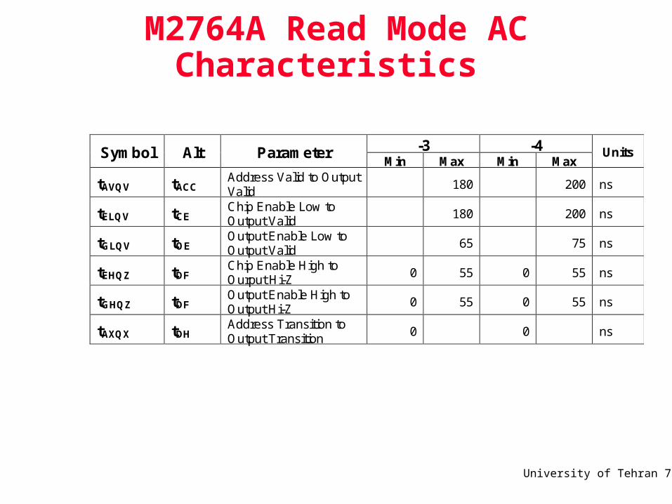
M2764A Read Mode AC Characteristics
-3 -4 Symbol Alt Parameter Min Max Min Max
Units
tAVQV tACC Address Valid to Output Valid
180 200 ns
tELQV tCE Chip Enable Low to Output Valid
180 200 ns
tGLQV tOE Output Enable Low to Output Valid
65 75 ns
tEHQZ tDF Chip Enable High to Ourput Hi-Z
0 55 0 55 ns
tGHQZ tDF Output Enable High to Output Hi-Z
0 55 0 55 ns
tAXQX tDH Address Transition to Output Transition
0 0 ns

University of Tehran 74
M2764A Read Mode Timing Diagram
University of Tehran 75
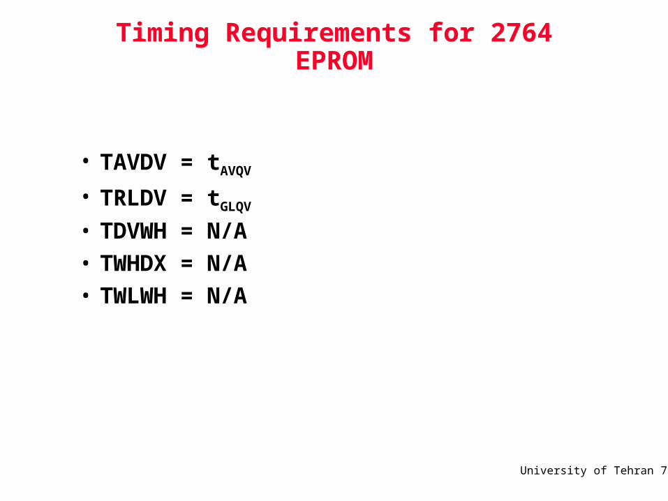
Timing Requirements for 2764 EPROM
• TAVDV = tAVQV
• TRLDV = tGLQV
• TDVWH = N/A
• TWHDX = N/A
• TWLWH = N/A

University of Tehran 76
Timing Requirements for 2764 EPROM
• TAVDV = tAVQV = ?
• TRLDV = tGLQV = ?
• TDVWH = N/A
• TWHDX = N/A
• TWLWH = N/A

University of Tehran 77
M2764A Read Mode AC Characteristics
-3 -4 Symbol Alt Parameter Min Max Min Max
Units
tAVQV tACC Address Valid to Output Valid
180 200 ns
tELQV tCE Chip Enable Low to Output Valid
180 200 ns
tGLQV tOE Output Enable Low to Output Valid
65 75 ns
tEHQZ tDF Chip Enable High to Ourput Hi-Z
0 55 0 55 ns
tGHQZ tDF Output Enable High to Output Hi-Z
0 55 0 55 ns
tAXQX tDH Address Transition to Output Transition
0 0 ns

University of Tehran 78
Timing Requirements for M2764A-3
• TAVDV = tAVQV = 180 ns
• TRLDV = tGLQV = 65 ns
• TDVWH = N/A
• TWHDX = N/A
• TWLWH = N/A

University of Tehran 79
Comparing Timing Requirements of 8088 (using 4 Mhz clock) and M2764A-3
8088 using 4MHz clk Timing Req. HM6264B-8L 610 ns TAVDV or tAVQV 180 ns
555 ns TRLDV or tGLQV 65 ns

University of Tehran 80
What if we need to interface a “slow” memory to the 8088?

University of Tehran 81
Comparing Timing Requirements of 8088 (using 4 Mhz clock) and a certain “slow” memory chip
8088 using 4MHz clk Timing Req. memory chip 610 ns TAVDV or tAA 85 ns
555 ns TRLDV or tOE 45 ns 400 ns TDVWH or tDW 40 ns
88 ns TWHDX or tDH 0 ns
440 ns TWLWH or tWP 500 ns

University of Tehran 82
8088Minimum
Mode
A12
A0:
D7
D0:
MEMRMEMW
A13A14
HM6264B-8L
A12
A0:
D7
D0:
OEWE
CS1 CS2
SLOWMEMORY
A12
A0:
D7
D0:
RDWR
CS
M2764A-3
A12
A0:
Q7
Q0:
G
C
A15A16A17A18A19
::
5V
READY

University of Tehran 83
Recall:Write Pulse Width / Write-Time (TWLWH)
ALE
T1
CLOCK
T2 T3 T4
AD7 - AD0
A15 - A8
A19/S6 - A16/S3
DT/R __
IO/M __
_____
WR
DEN______
A19 - A0from 74LS373 to memory
A15 - A8
A19 - A16 S6 - S3
A19 - A0 from 74LS373
A7 - A0 D7 - D0 (to 74LS245)
D7 - D0from 74LS245 to memory
D7 - D0 (to memory)A7 - A0
TWLWH
2TCLCL

University of Tehran 84
Write Pulse Width / Write-Time (TWLWH) w/ 1 wait state
ALE
T1
CLOCK
T2 T4
AD7 - AD0
A15 - A8
A19/S6 - A16/S3
READY
IO/M __
_____
WR
DEN______
A19 - A0from 74LS373 to memory
D7 - D0from 74LS245 to memory
TWLWH
A7 - A0 D7 - D0 (to memory)
A7 - A0 D7 - D0 (to 74LS245)
A15 - A8
A19 - A16 S6 - S3
A19 - A0 from 74LS373
DT/R __
TW T3
University of Tehran 85
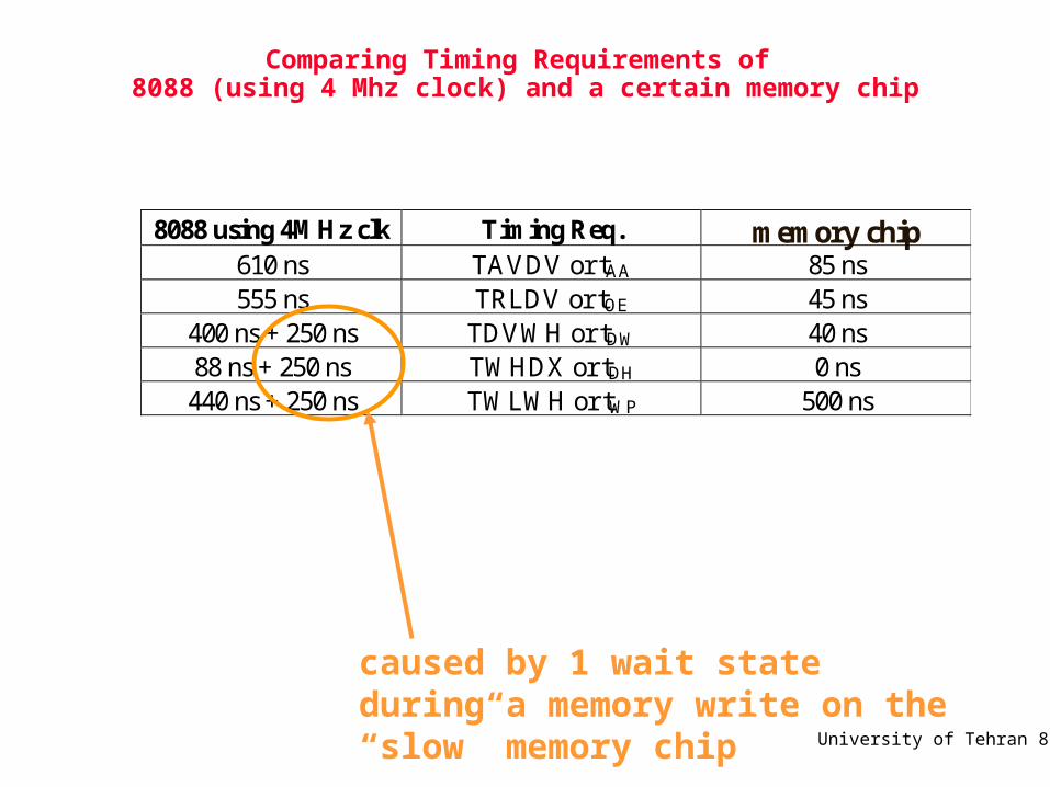
Comparing Timing Requirements of 8088 (using 4 Mhz clock) and a certain memory chip
8088 using 4MHz clk Timing Req. memory chip 610 ns TAVDV or tAA 85 ns
555 ns TRLDV or tOE 45 ns 400 ns + 250 ns TDVWH or tDW 40 ns
88 ns + 250 ns TWHDX or tDH 0 ns
440 ns + 250 ns TWLWH or tWP 500 ns
caused by 1 wait state during a memory write on the “slow” memory chip

University of Tehran 86
How do we produce a wait state?
• By turning the READY input of the 8088 microprocessor to LOW

University of Tehran 87
8088Minimum
Mode
A12
A0:
D7
D0:
MEMRMEMW
A13A14
HM6264B-8L
A12
A0:
D7
D0:
OEWE
CS1 CS2
SLOWMEMORY
A12
A0:
D7
D0:
RDWR
CS
M2764A-3
A12
A0:
Q7
Q0:
G
C
A15A16A17A18A19
::
5V
READY
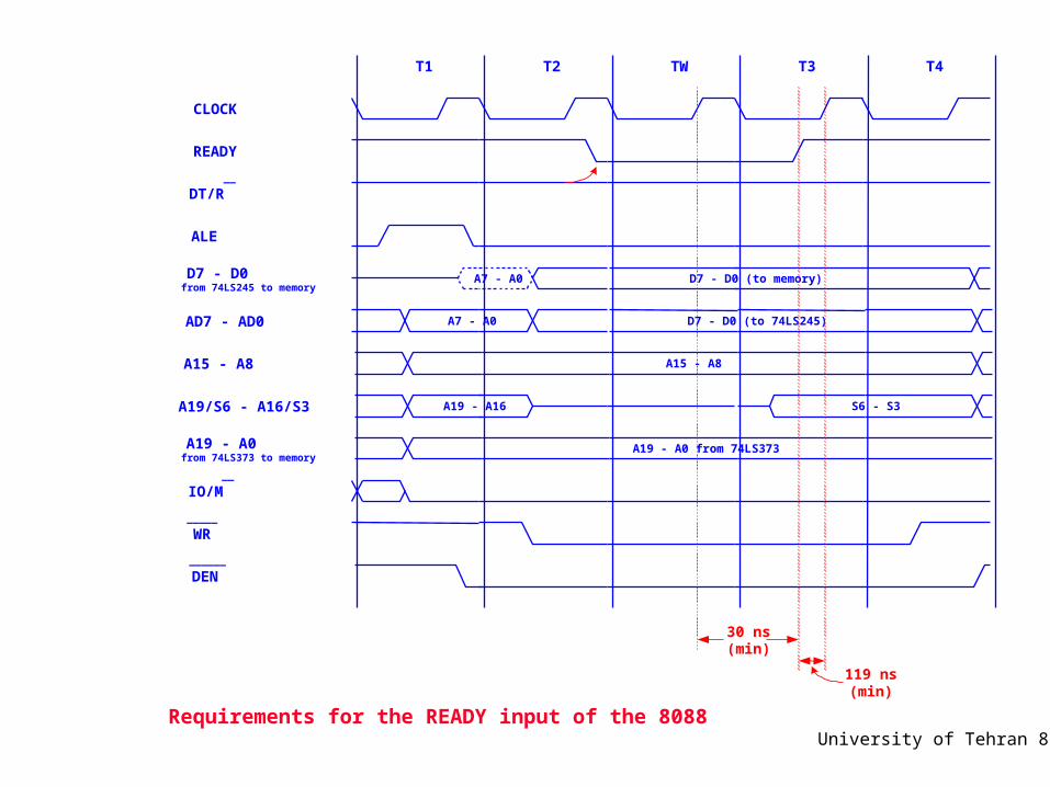
University of Tehran 88Requirements for the READY input of the 8088
ALE
T1
CLOCK
T2 T4
AD7 - AD0
A15 - A8
A19/S6 - A16/S3
READY
IO/M __
_____
WR
DEN______
A19 - A0from 74LS373 to memory
D7 - D0from 74LS245 to memory
30 ns(min)
A7 - A0 D7 - D0 (to memory)
A7 - A0 D7 - D0 (to 74LS245)
A15 - A8
A19 - A16 S6 - S3
A19 - A0 from 74LS373
DT/R __
TW T3
119 ns(min)
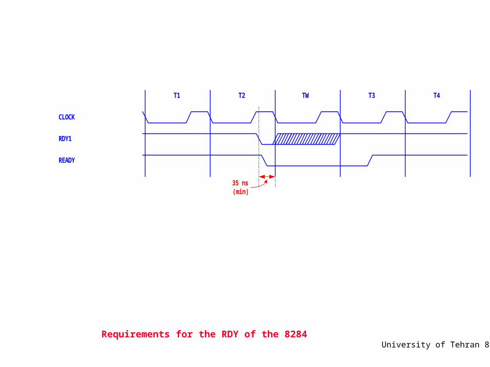
University of Tehran 89Requirements for the RDY of the 8284
T1
CLOCK
T2 T4
RDY1
35 ns(min)
TW T3
READY

University of Tehran 90
Memory
2 x m Bitn
m - Bit Data
n - Bit
Address
decoder
Address
Memory - Global Organisation

University of Tehran 91
Static vs Dynamic RAM
• SRAM vs DRAM
• DRAM stores charge in capacitor
– Disappears over short period of time
– Must be refreshed
• SRAM easier to use
– Faster
– More expensive per bit
– Smaller sizes

University of Tehran 92
Structure of SRAM
• Control logic
• One memory cell per bit– Cell consists of one or more transistors
– Not really a latch made of logic
• Logic equivalent

University of Tehran 96
16 X 1 RAM
What is this?

University of Tehran 97
Tri-State
• Have three states: H, L, and Hi-Z– High impedance
– Behaves line no output connection if in Hi-Z state
– Allows connecting multiple outputs
University of Tehran 98
Multiplexed with Hi-Z
• Normal behavior is blue areaSmoke

University of Tehran 99
Row/Column
• If RAM gets large, there is a large decoder
• Also run into chip layout issues
• Larger memories usually “2D” in a matrix layout
University of Tehran 100
16 X 1 as 4 X 4 Array
• Two decoders– Row
– Column
• Address just broken up
• Not visible from outside
University of Tehran 101
Change to 8 X 2 RAM
• Minor change in logic
• Also pinouts
• Address 011 (for example)
University of Tehran 102
m - Bit DataColumn Address DecoderColumn selection
RowAddressDecoder
Memory cell
Quadratic
Memory Matrix
2 Lines (Bit Lines)n / 2
- Bit Column Addressn / 2
- Bitn / 2
Row Address
n - Bit Address
2 Linesn / 2
(Word Lines)
m Level
W/E CS OE PGM
Control Logic
Memory - Internal Organisation

University of Tehran 104
SRAM Performance
• Current ones have cycle times in low nanoseconds (say 2.5ns)
• Used as cache (typically offchip secondary cache)
• Sizes up to 8Mbit or so for fast chips
• SRAMs:– Asynchronous
– Synchronous
University of Tehran 105
Micron SRAMs
• SyncBurst
• ZBT
• QDR
• DDR (common IO)
• DDR (separate IO)
• Synchronous
• Control inputs are captured at clock edges

University of Tehran 106
SRAM Categories
• SYNCBURST– Internal 2-bit burst counter– Appropriate for cache line size of four– Two bus master support (CPU and cache controller)– ADV# controls number of words– Not suited for more frequent bus turnaround applications
• ZBT (Zero Bus Turnaround)– Internal 2-bit burst counter– FLOW-Through ZBT
» One clock cycle delay» Less data latency and less frequency
– Pipelined ZBT» While data is delivered the memory array is free for the next
data access» Higher frequency

University of Tehran 107
Pentium Cache System
University of Tehran 108
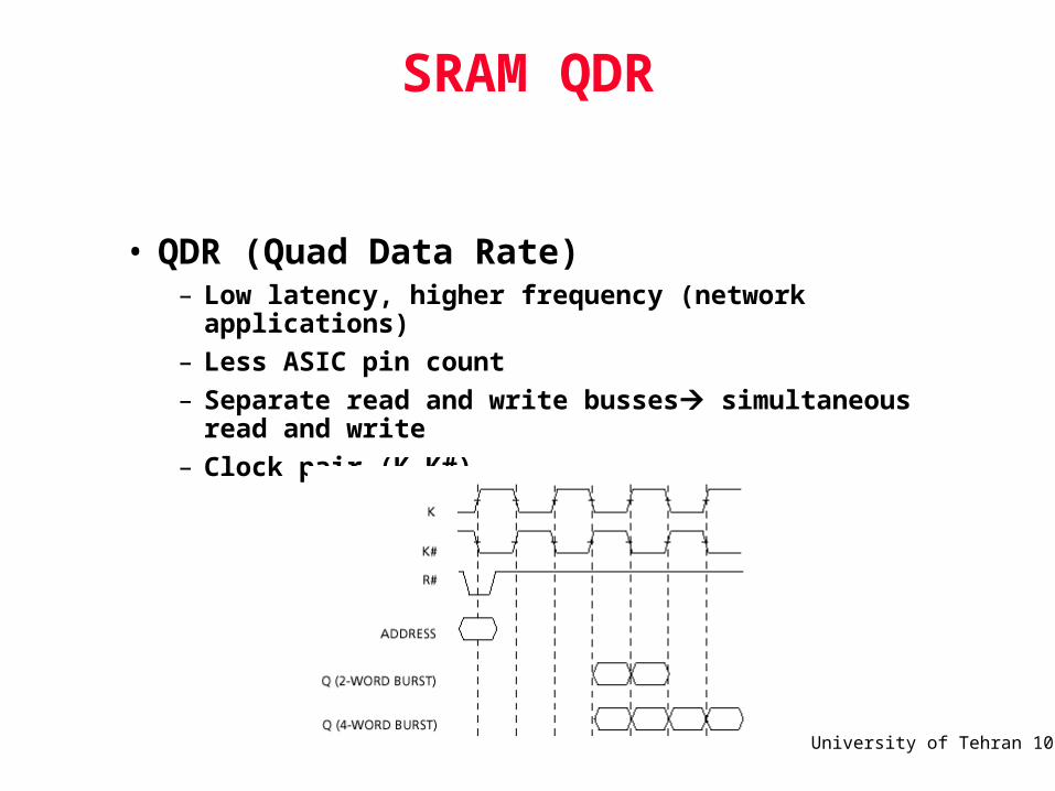
SRAM QDR
• QDR (Quad Data Rate)– Low latency, higher frequency (network applications)
– Less ASIC pin count
– Separate read and write busses simultaneous read and write
– Clock pair (K,K#)
University of Tehran 109
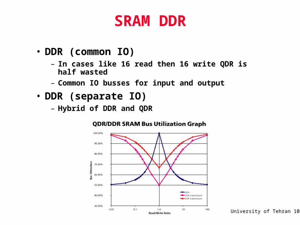
SRAM DDR
• DDR (common IO)– In cases like 16 read then 16 write QDR is half wasted
– Common IO busses for input and output
• DDR (separate IO)– Hybrid of DDR and QDR