
University of Minnesota Department of Electrical and Computer...
32
University of Minnesota Department of Electrical and Computer Engineering EE 3006 Laboratory Manual An Introductory Circuits/Electronics Laboratory for Non-ECE Majors
Transcript of University of Minnesota Department of Electrical and Computer...
University of Minnesota
Department of Electrical and Computer Engineering
EE 3006 Laboratory Manual
An Introductory Circuits/Electronics Laboratory
for Non-ECE Majors

General Information
Course Objectives This course was designed with several objectives in mind. First, it is intended to supplement the lecture course EE3005 and can only be carried out with the maximum benefit if you are acquainted with the topics being discussed there. The experimental topics are synchronized with the EE3005 lectures so that EE3005 covers the topics either before the experiment is done or while the experiment is being carried out. Second, the laboratory is intended to develop your self-confidence in laboratory procedures and in drawing conclusions from observations. As a consequence the instructions are sparse and assume you will be able to extract conclusions from each experiment and will relate parts of the total lab to each other without being explicitly asked to do so. In particular the laboratory manual will not specify what typical results you should expect from your measurements. In most cases you will be able to estimate what values to expect as part of your preparation before coming to the laboratory to do the experiment. Grading Your grade in this course will depend principally on your in-lab work. Grades will be determined from the following components of the course:
Lab Notebooks and class participation (attendance)- 50% Lab Practical Exams - 50% Take them seriously, they are forty minutes to one hour in duration and they account for a significant portion of your final grade.
Lab notebooks will be collected up to three times during the semester. Consult your TA for dates and procedures.
Late Penalties. The penalties for late notebooks are as follows: 1 or 2 days late: 3% deducted from your FINAL SCORE (total score for the entire course, not just the lab notebook). 3 or 4 days late - an additional 3% deducted from your FINAL SCORE. and so on...
Lab Notebooks You are expected to maintain a lab notebook. It must contain a running account of the experiment. It is not intended to be a book into which you copy notes previously gathered on the back of an envelope. It must however be legible and coherent. Write in such a way that another person could perform the same experiment based on your account, and that same person could understand the conclusions that you drew from your data. It is not necessary to hide your mistakes. If you make a mistake in an entry simply draw a line through that entry and start over - you will not be penalized for this. The lab notebook should have the following characteristics: - It should be a bound notebook (spiral bound is OK).

- Lab entries should be dated, and should include: - Complete circuit diagrams. - Explanation of circuit, methods, procedures, etc. - All calculations for designs. - All measurements (including component values). - All analysis and comparisons of data with theory. Milestones In each experiment there will be a few “milestones”. These are specific tasks which must be accomplished and demonstrated to the TA or professor before going on to the next item. All milestones must be completed or you will not pass the course. The TA will record (in ink) his name, date, and milestone number in your lab notebook when you have completed the milestone. If the milestones are not completed by the end of the semester you will receive an F for the course. While the milestones are not a part of the grade formula, delays in milestone completion will unavoidably delay the submission of your lab notebook with the corresponding grade penalty. Lab notebooks will not be accepted if the milestones for the corresponding lab have not been completed. Preparation There is no formal lab homework or pre-lab work in this course although there may be some problems or exercises suggested in some experiments as preparation. It will pay great dividends for you to make a careful reading of the experiment description before arriving in the laboratory. You will also note that some parts of the "experiments" involve analytical work which can be better done elsewhere. Most problems students have with this course are due to lack of preparation prior to coming to lab. If after reading through the lab and consulting the relevant section of your EE3005 text you do not understand something, seek out either your TA or the faculty member in charge of the lab.

Experiment #1
Introduction to EE3006 and Equipment Familiarization
Sessions 1 and 2 Introduction The lab instructor will go over the procedures and expectations for this course. He will then demonstrate the use of the computer controlled PXI-buss based digital multimeter (DMM), oscilloscope, function generator, dc power supply, and how to wire circuits on the protoboard in each student lab kit. The student should then spend the rest of the lab period trying out the equipment to become more familiar with it. Measurements 1. Connect the 6V dc supply terminals from the DC power supply to the PXI-based DMM and the stand-alone DMM as shown in Fig. 1-1. Vary the setting of the dc output and compare with the reading of the DMMs. Be sure that the DMMs are set to read DC volts.
PXI-based DC
Power Supply
PXI-based
DMM
Stand-alone
DMM
0-6V
+
-
0-20V
0-20V-
-
+
+
Figure 1-1. Connection of dc power supply and digital multimeters (DMMs) for measuring dc voltage.
2. Repeat step #1 for the 0 to +20 supply and then the 0 to -20 supply. 3. Display a 4 V peak-to-peak sinewave at a frequency of 1 kHz on the oscilloscope. Connect the function generator to the oscilloscope as shown in Fig.1- 2 to obtain the display. Adjust both the vertical sensitivity (volts per division) and horizontal (time base) sensitivity (seconds, milliseconds, microseconds) to obtain a good display showing two or three cycles of the waveform.

PXI-based
Oscillosope
PXI-based
Function
Generator
Outer case of BNC Connector is connected to
power system ground (3rd prong on AC plug).
CH 0 is
output of
function
generator
Use either Ch 0
or Ch 1 on
oscilloscope
PXI-based
DMM
Figure 1- 2. Connection of function generator to oscilloscope for displaying and measuring ac waveforms. The connection of the DMM to measure rms voltages is also shown.
4. Measure the amplitude of this ac waveform with the DMM set on the ac voltage mode. Compare this reading with the base-to-peak value you observe on the oscilloscope. The voltage measurements in steps #3 and step #4 should have different values. The DMM is calibrated to display the rms value of a sinewave which equals 0.707 of the base-to-peak value of a sinewave. Other waveforms such as square waves and triangular waves will have different rms-to-base-to-peak ratios as measurements of step #5 will illustrate. 5, Repeat steps #3 and #4 with square waves and then triangle waves. A square wave has an rms value which is equal to the base-to-peak value. A triangle wave has an rms value value which is 0.578 of the base-to-peak value. . 6. Construct the circuit shown below in Fig. 1-3, sometimes termed a voltage divider. Use a 4 V peak-to-peak 1 kHz sinewave for the input and measure the output voltage with the oscilloscope and DMM. The point of this step is to become familiar with using the protoboard to construct circuits and make connections to sources and measurement instruments. Examine the layout of the protoboard shown below in Fig. 1-4 and note that a specific column of component insertion holes are shorted together. Each individual terminal of a component should be inserted into a separate column as illustrated for a resistor unless it is desired to have terminals shorted together. Electrical connections to the function generator and oscilloscope are made via so-called BNC connector terminals. The outer cases of these connectors are directly connected to the ground (ground pin) of the ac power plug. When these instruments are connected to the AC power outlets, all of the instruments grounds (BNC outer cases) are shorted together as indicated in the figure. Any instrument that connects to the AC power system is configured in this manner (for

reasons of safety). Thus it is not possible to connect the oscilloscope so as to measure the voltage across the 4 kΩ resistor because the 1 kΩ resistor would then be shorted out.
4 kΩ
1 kΩVin Vout
+
-
+
-
functiongenerator oscilloscope
AC (110 V rms 60 Hz) power outlets
protoboard
built-in ground connections
Fig. 1-3. Voltage divider circuit and instrument grounding.
componentinsertion columns
componentinsertion columns
connection rows for off-board connections (dc power, signals, measuring insruments etc.)
insertion hole on protoboard
built-in electrical connection (short) between insertion holes
connection rows for off-board connections (dc power, signals, measuring insruments etc.)
Fig. 1-4. Diagram of protoboard which is used to construct circuits for laboratory measurements. 7. Replace the function generator with the 0-6V dc power supply and repeat step #6. 8. Construct the circuit of Fig. 1-5. Set the DMM to measure dc currents. In this configuration the DMM is being used to measure current.

1 kΩ+
-
AC (110 V rms 60 Hz) power outlets
protoboard
built-in ground connections
PXI-based DMM
PXI-based DCPower Supply Vdc
I dc
Figure 1-5. Circuit arrangement for measuring current through a resistor.
Compare the current measured by the DMM with the current output indicated by the dc power supply display. They should be the same. 9. Construct the circuit of Fig. 1-6 and use it to measure the resistance of several of the resistors in your lab kit. Make sure to use the proper set of terminals on the DMM and set the DMM to measure resistance.
protoboard
PXI-based
DMMR
Figure 1-6. Circuit for determining values of resistors. Compare the reading of the DMM with the value of resistance indicated by the color code on the resistor body.

Experiment #2
Voltage and Current Measurements and Voltage Source Characterization
Sessions 3 and 4 Introduction This experiment will familiarize you with simple resistive circuit measurements and acquaint you with the nonideal characteristics of voltage and current measuring instruments. The experiment will characterize voltage and current divider circuits and Thevenin equivalent circuits. Measurements Thevenin Equivalent Circuit of a Battery Ideal voltage sources put out a fixed voltage regardless of how much current is drawn from them as is shown in Fig. 2-1 by the curve labeled ideal. Real voltage sources such as batteries deliver a voltage at their output terminals which decreases as the current drawn from the voltage increases. This is illustrated in Fig. 2-1 by the curve labeled realistic. The Thevenin equivalent circuit of a physically realizable voltage source is shown in Fig. 2-1.
V
i
Vs
Rs
+
-
+
-
Thevenin equivalentcircuit of battery
V
i
ideal
realistic
Vs
0
Fig 2-1. Ideal versus real voltage sources and their Thevenin equivalent circuits.
1. Measure the open-circuit-voltage of a nominal 1.5V AAA battery to the nearest millivolt. 2. Determine experimentally the value of a resistor, that, when placed across the battery, will make a measurable change in the measured battery voltage.

Select resistor values to try with some care in mind - the battery can be damaged by excessive current draw. Keep the voltage decrease from the open circuit value to 10% or less, i.e. the loaded (external resistor across the battery) battery voltage should be ≥ 90% of the open circuit value. 3. Measure the resistance value found in step #2 directly with the DVOM in the resistance mode. Calculate the internal resistance of the battery. Voltage Divider and Voltage Measurements Voltage measuring instruments such as oscilloscopes and voltmeters (such as the DMM) are connected in parallel (shunt) with the terminal pair across which the voltage is to be measured as is shown in Fig. 2-2. Ideally the voltmeter does not perturb the circuit operation which implies that the voltmeter draws no current (RVM in Fig. 2-2 infinite). In real voltage measuring instruments, this is not the case. For example the oscilloscope has RVM = 1MΩ unless a 10:1 probe is used in which case RVM = 10 MΩ. The DMM also has RVM = 1MΩ.
+
-
+
-VR
vm
Voltmeter
equivalent
circuit
R1
R2V
B VR2
Fig. 2-2. Voltmeter connected to a voltage divider circuit.
4. Design a voltage divider to provide a voltage that is approximately 1/3 of the battery voltage. Use resistances in the kΩ range and measure the output of your divider when driven by the battery. 5. Redesign your divider so that the resistors are in the MΩ range and measure the output. Compare the results with the result of step #3 and with theory. ____________________________________________________________________________ MILESTONE #2-1: Demonstrate your voltage divider of step #5. Be prepared to show how it compares with theory. ____________________________________________________________________________ Current Divider and Current Measurements Current measuring instruments (generically termed ammeters) such the DMM are connected in series with the component through which the current to be measured is flowing as is shown in Fig. 2-3. Ideally the ammeter does not perturb the circuit operation which implies that there is no voltage drop across the ammeter (RAM in Fig. 2-3 is zero). In real ammeters. RAM > 0.

Rs
+
-Ammeter
equivalent
circuit
R1
R2
VB
A
Ram
I2
Fig. 2-3 Ammeter connected to a current divider circuit. 6. Design a current divider that will provide a 1/3 - 2/3 current splitting ratio. Use resistances in the kΩ range and power the circuit from the 1.5 V AAA battery. Measure the current splitting ratio. You will need to place a resistor (RS in Fig. 3) in series with this current divider in order to keep the current at a reasonable level. 7. Redesign the current divider so that the resistors are less than 100 ohms but maintain the same 1/3 - 2/3 splitting ratio. Again use a third resistor in series with the divider to keep the current at a reasonable level. Measure the current splitting ratio. Compare this result with that of step #6 and theory. 8. Repeat steps 1-3 using the function generator. Use a sinewave and set the open circuit voltage of the function generator to 4 V peak-to-peak and a frequency of 1 kHz. _____________________________________________________________________________ MILESTONE #2-2: Demonstrate the reduction in the measured function generator output voltage when loaded with the resistor. Be prepared to explain how you estimated the source resistance of the function generator. _____________________________________________________________________________

Experiment #3
Transient Response of RC and RLC Circuits Session 5 Introduction This experiment will explore the transient behavior of simple RC and RLC circuits. Experimental techniques for determining time constants and rise and fall times will be demonstrated. Measurements Time Constants and Rise Time Measurement 1. Construct a simple RC single time constant circuit of the form shown. Choose component values such as to make the time constant about 0.1ms and determine the time constant experimentally by observing resistor and capacitor voltages when a square wave is applied to the input port. Use a frequency whose period is 6-10 time constants in length.
Fig. 3-1. Single time constant circuit (a) with time constant τ = RC. Square wave input signal
Vin and resulting output signal Vout are shown in (b). Rise time tr and fall time tf are defined on the output waveform in (c).
2. Determine the rise and fall times of the output waveform for the circuit in step #1. The rise time is the time required for a waveform to rise from 10% of its final value to 90% of its final value. The fall time is the time required for the waveform to fall from 90% of the initial
-
+
Vout
+
C
R
Vin
(a)
90%
10% 90%
10%
tf
t r
Vout
(c)
-Vs
Vs
T
t
t
o
o
Vs
-Vs !
Vs V
s- 2 e
-t/!
-t/!V
s Vs
2 e- +
Vin
(b)
2Vs
e- Vs
2 V (1 - 1/e)s

value to 10% of the initial value. These quantities are shown graphically in Fig. 4-1c. Theoretically it can be shown (you should derive this before coming to class) tr = tf = 2.2RC. _____________________________________________________________________________ Milestone 3-1. Demonstrate the measurement of rise and fall time in step #2. _____________________________________________________________________________
Differentiator 3. Select values for R and C in the differentiator circuit shown in Fig. 4-2 so that a sharp spike will be produced whenever the square wave input changes sign. The square wave is to hae a frequency of 20 kHz.
Fig. 3-2. Differentiator circuit which produces a sharp spike at its output when the input is a
square wave. Many applications require that a sharp pulse be generated to mark the time at which a rapid change occurs in a signal. Transient Behavior of RLC Circuits 4. Design and construct the series RLC circuit shown in Fig. 3-3. The circuit to have a resonant frequency fo = 5 KHz and a Q = 5 = (2π fo )/(2α) where α = R/(2L). Use the 10 mH or 100 mH inductor in your lab kit (which ever one you have).
Vi V
oC
R
+
--
+
Vo
Vi
t
t

Figure 3-3. Series RLC circuit. 5. Drive the circuit of step #4 with a 100 Hz square wave and observe the voltage across the resistor. Repeat for a square wave of 5 kHz.
LC
RVi V
o
+
-
-
+

Quiz
Covers Experiments 1,2, and 3 Session 6
Duration: Full 2 hour lab period if needed.
Open lab notebook and EE3005 textbook

Experiment #4
RC and RLC Networks: Frequency Response and Filters
Session 7 and 8 Introduction In this lab you will determine the sinusoidal steady state responses of various RC and RLC networks and study some examples of their use in circuit design and applications. Measurements RC Low Pass Filter 1. Construct the RC circuit shown below. Choose component values so that the cutoff frequency (fc = 1/2πRC ) equals 5 kHz.
Fig. 4-1. RC low pass filter. 2. Investigate the amplitude (magnitude) and phase of the output of the RC circuit in item 1 as the frequency of the driving sinusoid is varied over a suitably wide range (at least 0.1fc. < f < 10fc). Determine the frequency at which the amplitude (magnitude) is down to 0.707 of the value it has in the low-frequency limit. Also determine the frequency at which the output is phase shifted by 45 degrees with respect to the input. Consult your lab instructor if you are unsure how to measure the phase shift versus frequency. You should be able to derive the transfer function magnitude and phase versus frequency equations given above as well as the cutoff frequency. You should also approximately plot these equations over the same frequency range as specified in the measurements before coming to lab. _____________________________________________________________________________ Milestone #4-1. Demonstrate the operation of your low pass filter to your instructor. Explain how you determined the 3db cutoff frequency. _____________________________________________________________________________
Vout
Vin = magnitude of transfer function
Vout
Vin =
11 +(2πfRC)2
<) (Vout/Vin) = phase angle of transfer function <) (Vout/Vin) = - tan-1(ωRC)

RC High Pass Filter 3. Modify the circuit of step #1 by interchanging positions of the resistor and capacitor as is shown in Fig. 4-2. Keep the components values the same as in step #1.
C
RVin
Vout
+
- -
+
Fig. 4-2. RC high pass filter. 4. Repeat the measurements of step #2 on the circuit of Fig. 4-2. The cutoff frequency of the high pass filter is given by the same equation as for the low pass filter, but the 0.707 point is with respect to the high frequency limit of the transfer function magnitude. Coupling and Blocking Capacitors 5. Construct and test the circuit shown in Fig. 4-3 which will generate a 5 + 1 sin( 2 π f t ) V signal, with f = 10 kHz.
C
R
Vout
- -
+
V sin(2!ft)s
+
VDC
+
-
Fig. 4-3. Use of a coupling capacitor to couple both DC and an AC signal to the output of circuit. The capacitor both couples the sinusoidal signal to the output of the circuit while
blocking the DC from getting to the AC source. Series Resonant Circuit 6. Design the series RLC circuit shown in Fig. 4-5 to have a resonant frequency fo = 5 KHz and a Q = 5. Measure the magnitude and phase of the transfer function Vo/Vi over a wide enough frequency range (0.1fo < f < 10fo) so that the complete frequency-dependent behavior of the transfer function is determined.
Vout
Vin = magnitude of transfer function
Vout
Vin =
2πfRC1 +(2πfRC)2
<) (Vout/Vin) = phase angle of transfer function
<) (Vout/Vin) = tan-1
1
2πfRC

Fig. 4-4. Textbook (ideal) series resonant RLC circuit.
C
V sin(2!ft)s
L
Vi
Vo
+
--
+
R wRs
Thevenin equivalent circuit
of function generator
R1
R = winding resistance of inductorw
Fig. 4-5. Practical realization of a series RLC circuit. In determining the Q of this circuit,
the total series resistance Rw + R1 equals the resistance R in the equation for Q.
In the equation for
Vout
Vin, R in the numerator is replaced by R1.
Use the 10 mH inductor in your parts kit. Measure the winding resistance of your inductor with the DDM. Be sure to measure the input voltage Vi at each measurement frequency as well as Vo. Vi will vary with frequency even if the amplitude control on the function generator is kept constant because of the nonzero value of the function generator source impedance Rs (measured
in Exp. #2) Experimentally the quality factor is defined as Q = foΔf where Δf is the difference
between the upper (greater than fo) 3db cutoff frequency and lower (less than fo) 3db cutoff frequency. The circuits of Fig. 4-4 and 4-5 implement a so-called bandpass filter function. _____________________________________________________________________________ MILESTONE #4-2: Demonstrate that the circuit has the proper resonant frequency and Q. _____________________________________________________________________________
LC
RVi V
o
+
-
-
+
Vout
Vin =
ωRC1 - ω2LC2 + ωRC2 ; ω = 2πf
<) (Vout/Vin) = tan-1
1 - ω2LC
ωRC
resonant frequency fo = 1
2π LC ; Q = 2πfoL
R

7. Determine the resonant frequency (fo) of the series RLC circuit of step #6 when the capacitor is varied from 0.001 µF to 0.1 µF. Compare the theoretical relationship between fo and C given above with that determined experimentally in step #7. Parallel Resonant Circuit 8. Design a parallel RLC circuit with a resonant frequency of 5 kHz and Q = 5. Measure the transfer function magnitude as a function of frequency over the same range as used in step #6.
R Vout
-
+
LCIs V
out
-
+
L
C
R
V = I Rs s
+
-
(a) (b) Fig. 4-6. Texbook parallel resonant circuit driven by a current source (a) and (b) the same
parallel resonant circuit driven by Thevenin equivalent circuit of current source Is and parallel resistance R.
The usual textbook example of a parallel resonant circuit is shown in Fig. 4-6. When a real ac voltage source with a finite value of source resistance is used to drive the circuit, the circuit diagram becomes as shown in Fig. 4-7. The winding resistance of the inductor can usually be ignored because it is in series with the inductance and the impedance of the inductor is much larger at frequencies of interest near the resonant frequency. Additionally the impedance of the parallel L-C combination is very large in the neighborhood of resonance.
-
+Vout-
+
LC
R
+
-
Vs
Rs
Vi
Fig. 4-7. Practical implementation of a parallel resonant circuit. 9. Design a circuit that strongly attenuates signals in a narrow bandwidth centered about 5 kHz (a so-called bandreject filter). Verify its proper operation.
Vout
Vin =
ωL
R21 - ω2LC2 + ωL2 ; ω = 2πf
<) (Vout/Vin) = tan-1
R(1 - ω2LC)
ωL
resonant frequency fo = 1
2π LC ; Q = 2πfoRC

Fig. 4-8. Bandreject filter
_____________________________________________________________________________ MILESTONE #4-3: Demonstrate your bandreject filter to the lab instructor. _____________________________________________________________________________
-
+Vout-
+
L
C
R
+
-
Vs
Rs
Vi
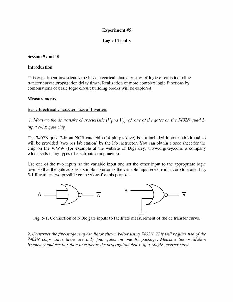
Experiment #5
Logic Circuits
Session 9 and 10 Introduction This experiment investigates the basic electrical characteristics of logic circuits including transfer curves,propagation delay times. Realization of more complex logic functions by combinations of basic logic circuit building blocks will be explored. Measurements Basic Electrical Characteristics of Inverters 1. Measure the dc transfer characteristic (VY vs VA) of one of the gates on the 7402N quad 2-input NOR gate chip. The 7402N quad 2-input NOR gate chip (14 pin package) is not included in your lab kit and so will be provided (two per lab station) by the lab instructor. You can obtain a spec sheet for the chip on the WWW (for example at the website of Digi-Key, www.digikey.com, a company which sells many types of electronic components). Use one of the two inputs as the variable input and set the other input to the appropriate logic level so that the gate acts as a simple inverter as the variable input goes from a zero to a one. Fig. 5-1 illustrates two possible connections for this purpose.
Fig. 5-1. Connection of NOR gate inputs to facilitate measurement of the dc transfer curve. 2. Construct the five-stage ring oscillator shown below using 7402N. This will require two of the 7402N chips since there are only four gates on one IC package. Measure the oscillation frequency and use this data to estimate the propagation delay of a single inverter stage.
A A
A
A

Fig. 5-2. Five-stage ring oscillator for measuring the propagation of an inverter. The output
waveforms for each of the five inverters is shown. _____________________________________________________________________________ Milestone #6-1. Demonstrate the operation of the ring oscillator and show your estimate of propagation delay to the instructor. _____________________________________________________________________________ 3. Verify operation of a NOR gate on the 7402N IC by direct measurements. 4. Construct a two-input OR gate using the 7402N chip. Verify operation as an OR gate by direct measurements.
Fig. 5-3. Two-input OR gate using NOR gate building blocks.
5V
Vo
Inverter
1
2
3
4
5
T
TpPropagation Delay
1 2 3 4 5
T = period of ring oscillator oscillation
T = T
10p
A
BA + B
A + B

5. Construct a two-input AND gate using the gates on the 7402N IC. Verify operation as a AND gate by direct measurements.
Fig. 5-4. Two-input AND gate using NOR gate building blocks.
6. Construct a two-input NAND gate using the 7402N IC. Verify operation as an NAND gate by direct measurements. 7. Construct an exclusive-OR gate using the 7402N ICs. Verify operation as an exclusive-OR gate by direct measurements.
A
B
A
B
A
B
A B
A B
A B A B+
A B A B+
Fig. 5-5. Two-input exclusive-OR gate using building block NOR gates.
_____________________________________________________________________________ Milestone #6-2: Demonstrate the operation of your exclusive-OR gate. _____________________________________________________________________________ 8. Construct an RS flip-flop using 7402N IC. Verify operation as an RS flip-flop by direct measurements.
A
B
A
B
A B+ = A•B

Reset R
Set S
Q
QS R Q Q
1 0 0 1
0 1 1 0
1 1 N/A N/A
0 0 Q Qoldold
Fig. 5-6. RS flip-flop implemented with NOR gates. The N/A (not applicable) entries in the truth
table mean that those combinations of inputs and outputs are not used because those states are unstable.

Experiment #6
Rectification and DC Power Supplies
Session 11 Introduction This experiment will introduce the rectification of ac signals into unipolar waveforms with significant dc content. These rectified waveforms will then be combined with a capacitor filter to realize an unregulated dc power supply. An integrated circuit voltage regulator will also be used to construct a regulated dc power supply. Measurements Half-Wave and Full-Wave Rectifiers 1. Examine the output of the circuit shown in Fig. 6-1 (termed half-wave rectifier) for 1 kHz sinusoidal input amplitudes from 0.5 V to 5V b-p.
Fig. 6-1. Half wave rectifier with input and output waveforms. The output waveform corresponds to Vs significantly larger than 0.7 volts.
Use the 1N4148 diode in this circuit and set R = 1kΩ. Use the DMM in DC voltage mode to measure the dc content of the output waveform when Vs = 5V. 2. Determine the effect of reversing the diode in the circuit of step #1. 3. Examine the output of the full-wave rectifier shown below for 100 Hz sinusoidal input amplitudes from 0.5 V to 5V b-p.
Vi VoR+
--
+
V sin(2πft)s
-Vs
Vs
sV - 0.7Vo
Vi
t
tV = sV - 0.7
DC π

Fig. 6-2. Full wave rectifier circuit and rectified output voltage for the case where the input Vs is
significantly larger than 1.4 V.
Use the 1N4148 diode in this circuit. Use the DMM in DC voltage mode to measure the dc content of the output waveform when Vs = 5V. Be observant of ground connections on measuring instruments and equipment to avoid unwanted short circuits. The function generator ground and the oscilloscope ground are both connected together. The oscilloscope channel A or B cannot be connected to the output Vo(t) without shorting out the diode on the lower right hand side of the diode bridge. Review the discussion on this topic in Experiment #1. If you have any questions, consult your lab instructor about how to measure the output voltage versus time with the scope. _____________________________________________________________________________ MILESTONE #6-1: Demonstrate the operation of the full-wave rectifier. _____________________________________________________________________________ Capacitor Filter with Full-Wave Rectifier 4. Place a 10 µF capacitor in parallel with the 1 kΩ as shown in Fig. 6-3. Otherwise the circuit ise the same as in Fig. 5-2. Determine the effect when Vs(t) is a 5 V b-p 100 Hz sinewave.
Fig. 6-3. Full-wave rectifier with capacitor filter. Output waveform corresponds to an input Vs significantly larger than 1.4V.
sV - 1.4
Vo
t
V (t)i
V (t) = V sin(2!ft)si
+
-
+
V (t) = ripple voltage
e-t/(RC)
sV - 1.4( )
C R
-
Vo
sV - 1.4
Vo
t
V (t)i 1
k!V (t)o
V (t) = V sin(2"ft)si
+
--
+
V = s(V - 1.4)
DC "
2

Be sure to observe the proper polarity when connecting the electrolytic capacitor. Measure the dc content of the waveform with the DMM and also determine the peak-to-peak magnitude of the ripple voltage. 5. Place a second 10 µF capacitor in parallel with the first and repeat step #4. Unregulated DC Power Supply with Transformer Isolation 6. Construct the unregulated dc power supply circuit shown below in Fig. 6-4. Determine both the dc voltage and ripple voltage as functions of the dc current through the load resistor. Limit the dc current to a maximum of 10 mA. Use the data to estimate the Thevenin equivalent circuit for the dc power supply.
Fig. 6-4. Unregulated DC power supply with transformer isolation.
The circuit should be constructed on the protoboard as much as possible. The transformer and diodes will be provided by the laboratory instructor. Do not use the diodes in your laboratory kit. They do not have the appropriate operating capabilities. In making measurements with the oscilloscope be careful to note that the outer conductor of the connector on the front panel is connected to the building ground (the third terminal on the ac power cord). If you put channel A of the scope across the transformer secondary and channel B across the load resistor, some of the diodes will be shorted out. The lab instructor will demonstrate the proper way to use the oscilloscope to obtain the needed information. _____________________________________________________________________________ MILESTONE #5-2: Demonstrate the operation of the unregulated dc power supply. Show the ripple voltage across the load for a 1 kΩ load resistor. _____________________________________________________________________________
V (t)o
50
µFR
L
I o +
-
110 V
rms
60 Hz
6.3 V
rms
60 Hz

Regulated DC Power Supply 7. Use the circuit of step #6 and the 7805T voltage regulator in your parts kit to make a 5 V regulated dc power supply. Repeat the measurements of step #6.
Fig. 6-5. Regulated DC power supply with transformer isolation. Read the specification sheet for the 7805T to determine how to use it. Limit the output current from your regulated supply to 20 mA max.
V (t)o
50
µFR
L
I o+
-
110 V
rms
60 Hz
6.3 V
rms
60 Hz
7805T

Quiz
Session 12 Covers Exps. 1-6

Experiment #7
Operational Amplifiers
Session 13 ad 14 Introduction This experiment will explore using integrated circuit operational amplifiers as the building block for a variety of different applications including various types of amplifiers and comparators. Be sure to get a complete set of specification sheets for the 741 op amp, including the pin-out configuration, before starting this experiment. Measurements Amplifiers Using Op Amps 1. Design a noninverting amplifier with a voltage gain of 10. Measure the transfer curve (Vo versus Vi) over the full range of input voltages.
Fig. 7-1. Non-inverting amplifier using an integrated circuit op amp.
Use resistor values for R1 and R2 in the 1-100 kΩ range. Use voltages of 10-15 volts for the two dc bias supplies required by the op amp. 2. Using resistors in the several kΩ range, design a voltage divider to produce an output of 5 V when the input is 15V. Determine the load on the divider which will drop the output voltage to 75% of its no load value. Review those sections of Exp. #2 dealing with voltage dividers. 3. Construct a buffer amplifier (non-inverting, gain of unity) using a 741.
-
+
R1
R2
Rs
Vs V
oVi
+
-
--
++
Vo
Vi
= 1 +
R2
R1
Vcc
-Vcc
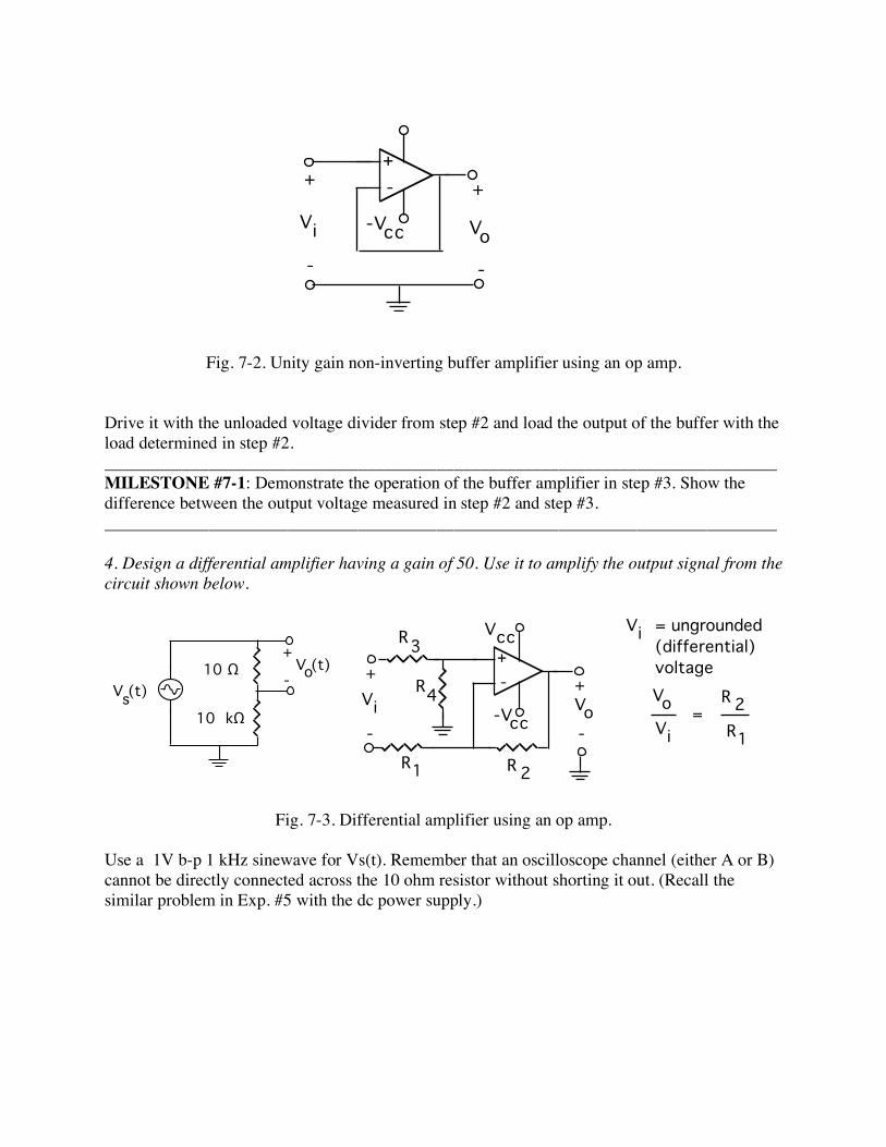
Fig. 7-2. Unity gain non-inverting buffer amplifier using an op amp. Drive it with the unloaded voltage divider from step #2 and load the output of the buffer with the load determined in step #2. _____________________________________________________________________________ MILESTONE #7-1: Demonstrate the operation of the buffer amplifier in step #3. Show the difference between the output voltage measured in step #2 and step #3. _____________________________________________________________________________ 4. Design a differential amplifier having a gain of 50. Use it to amplify the output signal from the circuit shown below.
Fig. 7-3. Differential amplifier using an op amp.
Use a 1V b-p 1 kHz sinewave for Vs(t). Remember that an oscilloscope channel (either A or B) cannot be directly connected across the 10 ohm resistor without shorting it out. (Recall the similar problem in Exp. #5 with the dc power supply.)
10 !
10 k!
V (t)s
V (t)o
+
-
-
+
+
-
Vo
Vi
+
-
-Vcc
-
+
R1 R 2
Vo
+
--
+Vo
Vi
= R 2
R1
Vi
Vcc
-Vcc
R3
R4
Vi = ungrounded
(differential)
voltage

Comparators 5. Construct the comparator circuit shown below. Monitor its output when the input is varied a few millivolts on either side of zero.
Fig. 7-4. Op amp-based comparator. 6. Interchange the roles of the input terminals and repeat step #5. 7. Design a circuit that will indicate whether an unknown voltage is greater or less than a given reference voltage. The reference voltage should be capable of being varied between -5V and +5V.
Fig. 7-5. Comparator with adjustable reference voltage. 8. Add red and green LEDs so that the green is on when the input voltage is less than the reference and the red when it is greater. The red and green LEDs are found in your parts kit. Use resistors in series with the LEDs to limit the total current through them to 20 mA maximum.
+
-
+-
5V
-5V
Vi V
o
+
-
-
-
-
+
+
Vo
Vi
++5V
-5V
-5V
+5V
adjustable reference voltage

Fig. 7-6. Comparator circuit with LED indicators.
Thermocouple Sensor The thermocouple is a device commonly used to measure temperature differences. Familiarize yourself with the operating characteristics of the thermocouple before continuing with this experiment. 9. Design an op amp interface between the copper-constantan thermocouple and the DVOM such that a 0 to 100 mV output will be obtained for a temperature range of 0 to 100 °C. Use an ice bath for the reference junction. Determine the thermocouple constant α so that the required op amp interface can be designed. Use the op-amp-thermocouple combination to determine the temperature of various items in the room.
Fig. 7-7. Copper-constantan thermocouple.
_____________________________________________________________________________ MILESTONE #7-2: Demonstrate your temperature measuring system at zero degrees C (ice water will be provided and body temperature). _____________________________________________________________________________
-
-
+
Vi
++5V
-5V
-5V
+5V
adjustable reference voltage
Red
LED
Green
LED
-
+
T2
T1
Vtc
copper
copper
constantan
ice water @ 0 ºC
(reference temp.)
= ! (T - T ) Vtc 2 1