University of Groningen Device physics of polymer Blom ...
17
University of Groningen Device physics of polymer Blom, Paul W. M.; Mihailetchi, Valentin D.; Koster, L. Jan Anton; Markov, Denis E. Published in: Advanced materials DOI: 10.1002/adma.200601093 IMPORTANT NOTE: You are advised to consult the publisher's version (publisher's PDF) if you wish to cite from it. Please check the document version below. Document Version Publisher's PDF, also known as Version of record Publication date: 2007 Link to publication in University of Groningen/UMCG research database Citation for published version (APA): Blom, P. W. M., Mihailetchi, V. D., Koster, L. J. A., & Markov, D. E. (2007). Device physics of polymer: fullerene bulk heterojunction solar cells. Advanced materials, 19(12), 1551-1566. https://doi.org/10.1002/adma.200601093 Copyright Other than for strictly personal use, it is not permitted to download or to forward/distribute the text or part of it without the consent of the author(s) and/or copyright holder(s), unless the work is under an open content license (like Creative Commons). The publication may also be distributed here under the terms of Article 25fa of the Dutch Copyright Act, indicated by the “Taverne” license. More information can be found on the University of Groningen website: https://www.rug.nl/library/open-access/self-archiving-pure/taverne- amendment. Take-down policy If you believe that this document breaches copyright please contact us providing details, and we will remove access to the work immediately and investigate your claim. Downloaded from the University of Groningen/UMCG research database (Pure): http://www.rug.nl/research/portal. For technical reasons the number of authors shown on this cover page is limited to 10 maximum. Download date: 15-02-2022
Transcript of University of Groningen Device physics of polymer Blom ...

University of Groningen
Device physics of polymerBlom, Paul W. M.; Mihailetchi, Valentin D.; Koster, L. Jan Anton; Markov, Denis E.
Published in:Advanced materials
DOI:10.1002/adma.200601093
IMPORTANT NOTE: You are advised to consult the publisher's version (publisher's PDF) if you wish to cite fromit. Please check the document version below.
Document VersionPublisher's PDF, also known as Version of record
Publication date:2007
Link to publication in University of Groningen/UMCG research database
Citation for published version (APA):Blom, P. W. M., Mihailetchi, V. D., Koster, L. J. A., & Markov, D. E. (2007). Device physics of polymer:fullerene bulk heterojunction solar cells. Advanced materials, 19(12), 1551-1566.https://doi.org/10.1002/adma.200601093
CopyrightOther than for strictly personal use, it is not permitted to download or to forward/distribute the text or part of it without the consent of theauthor(s) and/or copyright holder(s), unless the work is under an open content license (like Creative Commons).
The publication may also be distributed here under the terms of Article 25fa of the Dutch Copyright Act, indicated by the “Taverne” license.More information can be found on the University of Groningen website: https://www.rug.nl/library/open-access/self-archiving-pure/taverne-amendment.
Take-down policyIf you believe that this document breaches copyright please contact us providing details, and we will remove access to the work immediatelyand investigate your claim.
Downloaded from the University of Groningen/UMCG research database (Pure): http://www.rug.nl/research/portal. For technical reasons thenumber of authors shown on this cover page is limited to 10 maximum.
Download date: 15-02-2022

DOI: 10.1002/adma.200601093
Device Physics of Polymer:Fullerene BulkHeterojunction Solar Cells**
By Paul W. M. Blom,* Valentin D. Mihailetchi,L. Jan Anton Koster, and Denis E. Markov
1. Introduction
Harvesting energy directly from the sunlight using photo-voltaic (PV) technology is being widely recognized as an es-sential component of future global energy production. Pro-vided that PV devices can be made truly economicallycompetitive with fossil fuels and other emerging renewableenergy technologies, large-scale manufacturing of these de-vices offers a sustainable energy source that can supply a sig-nificant fraction of our daily energy needs. Photovoltaic cellshave become extensively studied since the 1950s when thefirst crystalline silicon solar cell, which had an efficiency of6 %, was developed at Bell Laboratories.[1] Since then, theefficiency has reached 24 % for crystalline Si solar cells,[2]
which is already close to the theoretical predicted upper limit
REV
IEW
Adv. Mater. 2007, 19, 1551–1566 © 2007 WILEY-VCH Verlag GmbH & Co. KGaA, Weinheim 1551
–[*] Prof. P. W. M. Blom, Dr. V. D. Mihailetchi, Dr. L. J. A. Koster,
Dr. D. E. MarkovMolecular ElectronicsZernike Institute for Advanced MaterialsUniversity of GroningenNijenborgh 4, 9747 AG Groningen (The Netherlands)E-mail: [email protected]
[**] The authors especially acknowledge the contributions of Kees Hum-melen, Bert de Boer, Jur Wildeman, Minte Mulder, Alex Sieval, andEdsger Smits to this work. These investigations were financially sup-ported by the Dutch Ministries of EZ, O&W, and VROM through theEET program (EETK97115). The work of L.J.A.K forms part of the re-search program of the Dutch Polymer Institute (# 323). The work ofD.E.M is part of the research program of the Stichting voor Fun-damenteel Onderzoek der Materie (FOM, financially supported bythe Nederlandse Organisatie voor Wetenschappelijk Onderzoek(NWO)).
Plastic solar cells bear the potential for large-scale power generation based on materials thatprovide the possibility of flexible, lightweight, inexpensive, efficient solar cells. Since the discov-ery of the photoinduced electron transfer from a conjugated polymer to fullerene molecules, fol-lowed by the introduction of the bulk heterojunction (BHJ) concept, this material combinationhas been extensively studied in organic solar cells, leading to several breakthroughs in efficien-cy, with a power conversion efficiency approaching 5 %. This article reviews the processes andlimitations that govern device operation of polymer:fullerene BHJ solar cells, with respect tothe charge-carrier transport and photogeneration mechanism. The transport of electrons/holesin the blend is a crucial parameter and must be controlled (e.g., by controlling the nanoscalemorphology) and enhanced in order to allow fabrication of thicker films to maximize theabsorption, without significant recombination losses. Concomitantly, a balanced transport ofelectrons and holes in the blend is needed to suppress the build-up of the space–charge that willsignificantly reduce the power conversion efficiency. Dissociation of electron–hole pairs at thedonor/acceptor interface is an important process that limits the charge generation efficiencyunder normal operation condition. Based on these findings, there is a compromise betweencharge generation (light absorption) and open-circuit voltage (VOC) when attempting to reducethe bandgap of the polymer (or fullerene). Therefore, an increase in VOC of polymer:fullerenecells, for example by raising the lowest unoccupied molecular orbital level of the fullerene, willbenefit cell performance as both fill factor and short-circuit current increase simultaneously.

of 30 %.[3,4] Practically all conventional inorganic solar cellsincorporate a semiconductor that is doped to form a p-n junc-tion across which the photovoltage is generated. The p sidecontains an excess of the positive charges (holes), and the nside contains an excess of the negative charges (electrons). Inthe region near the junction, an electric field is formed andthe electrons and holes, which are generated by light absorp-tion in the bulk Si, diffuse to this junction where they are di-rected by the electric field towards the proper electrode. Overthe years, solar cells have been made from many other semi-conductor materials with various device configuration such assingle-crystal, polycrystalline, and amorphous thin-film struc-tures. Organic materials bear the potential to develop a long-term technology that is economically viable for large-scalepower generation based on environmentally safe materialswith unlimited availability. Organic semiconductors are a lessexpensive alternative to inorganic semiconductors like Si.Compared to Si, they can have extremely high optical absorp-tion coefficients that offer the possibility for the production ofvery thin solar cells. Additional attractive features of organicPVs are the possibilities for thin flexible devices which can befabricated using high-throughput, low-temperature approach-es that employ well established printing techniques in a roll-to-roll process.[5,6] This possibility of using flexible plastic sub-strates in an easily scalable high-speed printing process canreduce the balance of system cost for organic PVs, resulting ina shorter energetic pay-back time.
The first investigation of an organic PV cell came as earlyas 1959, when an anthracene single crystal was studied. Thecell exhibited a photovoltage of 200 mV with an extremelylow efficiency.[7] Since then, many years of research has shownthat the typical power conversion efficiency of PV devicesbased on single (or homojunction) organic materials will re-main below 0.1 %, making them unsuitable for any possibleapplication. Primarily, this is due to the fact that absorption oflight in organic materials almost always results in the produc-tion of a mobile excited state (referred to as exciton), ratherthan free electron–hole (e–h) pairs as produced in inorganicsolar cells. This occurs because in organic materials the weakintermolecular forces localize the exciton on the molecules.Combined with a low dielectric constant (typically 2–4) com-pared to inorganic semiconductors, a much higher energy in-
put than the thermal energy (kT) is required to dissociatethese excitons.[8–10] The electric field provided by the asymme-trical work functions of the electrodes is not sufficient tobreak up these photogenerated excitons. Instead, the excitonsdiffuse within the organic layer until they reach the electrode,where they may dissociate to supply separate charges, orrecombine. Since the exciton diffusion lengths are typically1–10 nm,[11–15] much shorter than the device thicknesses, exci-ton diffusion limits charge-carrier generation in these devicesbecause most of them are lost through recombination. Photo-generation is therefore a function of the available mechanismsfor excitons dissociation. A major breakthrough in cell perfor-mance came in 1986 when Tang discovered that much higherefficiencies (about 1 %) can be attained when an electron do-nor (D) and an electron acceptor (A) are brought together inone cell.[16] This heterojunction concept is at the heart of allthree types of organic PV cells that currently exist: dye-sensitized solar cells;[17–19] planar organic semiconductorcells;[16,20–22] and high surface area, or bulk heterojunction(BHJ) cells.[5,23–25] The idea behind a heterojunction is to usetwo materials with different electron affinities and ionizationpotentials. At the interface, the resulting potentials are strongand may favor exciton dissociation: the electron will be ac-cepted by the material with the larger electron affinity andthe hole will be accepted by the material with the lower ion-ization potential, provided that the difference in potential en-ergy is larger than the exciton binding energy. In the planarheterojunction, or “bi-layer” device, the organic D/A inter-face separates excitons much more efficient than an organic/metal interface in the single layer device. In this device the ex-citons should be formed within the diffusion length of the in-terface. Otherwise, the excitons will decay, yielding, e.g., lumi-nescence instead of a contribution to the photocurrent. Sincethe exciton diffusion lengths in organic materials are muchshorter than the absorption depth of the film, this limits thewidth of effective light-harvesting layer. A revolutionary de-velopment in organic PVs came in the mid 1990s with the in-troduction of the dispersive (or bulk) heterojunction, wherethe donor and acceptor material are blended together. If thelength scale of the blend is similar to the exciton diffusionlength, the exciton decay processes is dramatically reducedsince in the proximity of every generated exciton there is an
REV
IEW
P. W. M. Blom et al./Device Physics of Polymer:Fullerene BHJ Solar Cells
1552 www.advmat.de © 2007 WILEY-VCH Verlag GmbH & Co. KGaA, Weinheim Adv. Mater. 2007, 19, 1551–1566
Paul W. M. Blom received his Ir. degree (Physics) in 1988 and his Ph.D. degree in 1992, from theTechnical University Eindhoven, Eindhoven, The Netherlands. Joining Philips Research Labora-tories in 1992 he was engaged in the electrical characterization of various oxidic thin-film devices,the electro-optical properties of polymer light-emitting diodes, and the field of rewritable opticalstorage. In May 2000 he was appointed as a Full Professor at the University of Groningen, wherehe leads a group in the field of electrical and optical properties of organic semiconductingdevices. At present the main focus is on the device physics of polymeric light-emitting diodes,transistors, solar cells, and molecular electronics.

interface with an acceptor where fast dissociationtakes place. Hence, charge generation takes placeeverywhere in the active layer. Provided that con-tinuous pathways exist in each material from theinterface to the respective electrodes, the photon-to-electron conversion efficiency and, hence, thephotosensitivity is dramatically increased.
One class of organic materials used as photoac-tive layer in bulk heterojunction PV cells that havereceived considerable attention in the last fewyears are semiconducting polymers and molecules.They combine the optoelectronic properties ofconventional semiconductors with the excellentmechanical and processing properties of “plastic”materials. Additionally, they possess an unprece-dented flexibility in the synthesis, allowing for al-teration of a wide range of properties, such as bandgap, mo-lecular orbital energy level, wetting and structural properties,as well as doping. This ability to design and synthesize poly-mers and molecules that can be cast from solution using wet-processing techniques such as spin-coating, ink-jet printing,and screen printing represents an enormous attractive routefor cheap production of large-area PV cells that can be ap-plied to systems that require flexible substrates. Because lumi-nescence quenching[26] and ultrafast photoinduced electrontransfer[27] from a conjugated polymer (as donor) to buckmin-sterfullerene (C60) or its derivatives (as acceptor) had alreadybeen observed in 1992, this material combination has been ex-tensively studied in bulk heterojunction PV cells. In 1995 Yuet al.[24] fabricated the first fully organic BHJ cell based on amixture of soluble p-phenylene vinylene (PPV) derivativewith a fullerene acceptor. In 2001, Shaheen et al.[28] obtainedthe first truly promising results for BHJ solar cells when mix-ing the conjugated polymer poly(2-methoxy-5-(3′,7′-dimethyl-octyloxy)-p-phenylene vinylene) (MDMO-PPV) and metha-nofullerene [6,6]-phenyl C61-butyric acid methyl ester(PCBM) in a 20:80 wt % and optimizing the nanoscale mor-phology of the film, yielding a power conversion efficiency of2.5 %. Recently, the attention has been shifted towards poly-mer:fullerene (like PCBM) BHJ solar cells based on polythio-phene derivatives as absorbing and electron donating materi-al.[29–33] By optimizing the processing conditions, efficienciesin excess of 4 % have been reported for this materials sys-tem.[34–36]
The fundamental physical processes in a BHJ device areschematically represented in an energetic diagram as depictedin Figure 1. Sunlight photons which are absorbed inside thedevice excite the donor (1), leading to the creation of excitonsin the conjugated polymer. The created excitons start to dif-fuse (3) within the donor phase and if they encounter the in-terface with the acceptor then a fast dissociation takes place(4) leading to charge separation.[27,37] The resulting metastableelectron–hole pairs across the D/A interface may still be Cou-lombically bound and an electric field is needed to separatethem into free charges.[38,39] Therefore, at typical operationconditions, the photon-to-free-electron conversion efficiency
is not maximal. Subsequently, the separated free electrons(holes) are transported (5) with the aid of the internal electricfield, caused by the use of electrodes with different work func-tions, towards the cathode (anode) where they are collectedby the electrodes (6) and driven into the external circuit.However, the excitons can decay (2), yielding, e.g., lumines-cence, if they are generated too far from the interface. Thus,the excitons should be formed within the diffusion length ofthe interface, being an upper limit for the size of the conjugat-ed polymer phase in the BHJ. In this review we will discussthese subsequent fundamental processes using a MDMO-PPV:PCBM (1:4 wt %) as a model system and evaluate theirrole for solar cell performance.
2. Physical Processes in Polymer:Fullerene BulkHeterojunction Solar Cells
2.1. Creation of Excitons
To reach a high efficiency, the active layer of a solar cellshould capture a large fraction of the incoming sun light. Be-cause of the high absorption coefficient (ca. 105 cm–1), conju-gated polymers absorb light very efficiently at the maximumof their absorption spectrum. As a result a layer thickness ofonly a few hundred nanometer is required to absorb all thelight at their peak wavelength absorption. As a comparison tosilicon based solar cells, active layer thicknesses of hundredsof micrometers are required since silicon is an indirect semi-conductor. However, because the absorption bands of conju-gated polymers are relatively narrow compared to inorganicsemiconductors, the performance of solar cells based on poly-mers is poor compared to inorganic solar cells. In an organicsolar cell, only a small region of the solar spectrum is covered.For example, a bandgap of 1.1 eV is required to cover 77 % ofthe AM1.5 (air mass) solar photon flux (assuming completeabsorption of the solar emission intensity by the material),whereas most solution processable semiconducting polymers(PPVs, poly(3-hexylthiophene) (P3HT)) have bandgaps largerthan 1.9 eV, which covers only 30 % of the AM1.5 solar
REV
IEWP. W. M. Blom et al./Device Physics of Polymer:Fullerene BHJ Solar Cells
Adv. Mater. 2007, 19, 1551–1566 © 2007 WILEY-VCH Verlag GmbH & Co. KGaA, Weinheim www.advmat.de 1553
Figure 1. Schematic band diagram of a) a bilayer device and b) a bulk heterojunction.The numbers refer to the operation processes explained in the text. The dashed linerepresents the energy levels of the acceptor, while the full lines indicate the energylevel of the donor in the PV cell. HOMO: highest occupied molecular orbital; LUMO:lowest unoccupied molecular orbital.

photon flux (assuming complete absorption of the solar emis-sion intensity by the material). In addition, as will be dis-cussed later, because of the low charge-carrier mobilities ofmost polymers, the thickness of the active layer is limited toca. 100 nm, which, in turn, results in an absorption of onlyca. 60 % of the incident light at the absorption maximum(without back reflection of the electrode).
When photons with energy beyond the absorption edge areincident on a semiconducting specimen of the polymer, anelectron and hole with opposite spin are created, bound bytheir Coulomb attraction in a singlet exciton state. Becausecoupling between neighboring molecules in molecular solidsis low, the molecular excitations are localized and there is noband to band transition, unlike in inorganic semiconductors.Concomitantly, the relative dielectric constant of the order of3, as compared to 10 in inorganic semiconductors, results instrongly bound Frenkel-like localized excitons. Hence, excitoneffects are important at room temperature, in contrast to inor-ganic Wannier-type excitons with a binding energy of aboutkT at room temperature. An important question is the magni-tude of the binding energy (EB) of the exciton in conjugatedpolymers. The disorder present in conjugated polymers pre-vents the exciton binding energy from being a well-definedmaterial quantity. The activation energy of photoconductivityin PPV-type systems cannot be used to characterize the exci-ton binding energy because extrinsic effects usually prevail incharge-carrier formation from the singlet exciton S1 state. Al-though it has been suggested that EB is of the order of, or lessthan kT,[40] there is a large amount of experimental evidencefor a much stronger binding. A Monte Carlo simulation studyhas been conducted to model bimolecular charge recombina-tion, treated as a random walk of a pair of charges in an ener-getically roughened landscape, with superimposed long-rangecoulomb interactions.[41] This analysis has demonstrated thatthe effective recombination cross-section of a charge carrierdecreases sharply as EB decreases. Under the conditionEB ≤ kT, the probability for recombination of a pair of chargecarriers is almost two orders of magnitude less than the re-combination required to explain the performance of polymer-based light-emitting diodes (LEDs). On the other handEB > 0.2 eV granted a sufficient recombination cross section.The exciton binding energy has been experimentally derivedfrom studies of the photovoltaic response of PPV based di-odes, leading to an exciton binding energy of approximately0.4 eV.[10] One of the most convincing quantitative assess-ments of the exciton binding energy magnitude is provided bystudying the photoluminescence quenching resulting from anelectric field.[42,43] The dissociation of an excited singlet stateof a conjugated polymer requires field-assisted transfer of theconstituent charges to a neighboring chain or chain segment.In a first order approximation, this would occur if the gain inelectrostatic energy, eEDz, where e is the electric charge, Ethe internal electric field, and Dz the distance between thecharges, compensates for the energy expense for the chargetransfer in zero field. Using Dz = 10 Å and E = 2 × 10⁶ V cm–1,leads to a eE Dz = 0.2 eV. Indeed, considerable steady-state
photoluminescence (PL) quenching has been observed forfilms of poly-(phenyl-p-phenylene vinylene)/polycarbonate(PPPV/PC) blends upon application of an electric field of thisorder of magnitude. Monte Carlo simulations of the field de-pendence of PL quenching give a good fit to experimentaldata for values of EB = 0.4 ± 0.1 eV. Besides field-assisted ex-citon dissociation, these simulations take into account radia-tive decay, energy relaxation within an inhomogeneouslybroadened density of states, and exciton capture by nonradia-tive traps.
2.2. Diffusion of Excitons in Conjugated Polymers
Because of the high exciton binding energy in conjugatedpolymers, the thermal energy at room temperature is not suf-ficient to dissociate a photogenerated exciton (typical bindingenergy of 0.4 eV) into free charge carriers. Consequently, theconfiguration and operation principle of photovoltaic devicesbased on organic semiconductors differ significantly fromthose based on inorganic materials. Typically, in organic solarcells an efficient electron acceptor is used in order to dissoci-ate the strongly bound exciton into free charge carriers.[16]
The exciton diffusion length LD, which characterizes the ef-fective width of the active area of the polymer film at theacceptor interface, has been reported to be 5–8 nm in PPV-based conjugated polymers.[12,14,15] Because the exciton diffu-sion length in a conjugated polymer is typically less than thephoton absorption length (ca. 100 nm), the efficiency of a bi-layer cell is limited by the number of photons that can be ab-sorbed within the effective exciton diffusion range at the poly-mer/electron acceptor interface. To circumvent the problemof limited exciton diffusion length in conjugated polymers, thebulk heterojunction PV cell architecture has been developedby simply blending the polymer with a soluble electron accep-tor.[23,44] In the ideal case, the characteristic (reduced) size ofthe polymer phase in the active layer of the cell grants that allexcitons are formed within the diffusion distance from anelectron acceptor interface. As a result, such an interpenetrat-ing donor:acceptor network allows photon absorption im-provement by a simple increase of the active-layer thickness,thereby maintaining an efficient dissociation of excitons. Exci-ton diffusion is therefore a beneficial process for polymer-based PV cells because it governs the transfer of the photoex-citation energy towards the electron donor/acceptor interface,where charge carriers are formed. Improvement of the exci-ton diffusion allows for bigger sized polymer domains leadingto an enhanced absorption and solar cell performance.
The exciton diffusion lengths in various conjugated poly-mers reported in the literature show a large variation, rangingfrom 5 to 20 nm.[12,45–49] Most of these studies make use of abilayer model system, comprising of an evaporated C60 layerin combination with a conjugated polymer spin-coated fromthe solution. From photocurrent measurements on the precur-sor poly(p-phenylene vinylene) (PPV)/C60 photovoltaic de-vices an exciton diffusion length of 7 ± 1 nm has been de-
REV
IEW
P. W. M. Blom et al./Device Physics of Polymer:Fullerene BHJ Solar Cells
1554 www.advmat.de © 2007 WILEY-VCH Verlag GmbH & Co. KGaA, Weinheim Adv. Mater. 2007, 19, 1551–1566

duced.[12] In this work it was stressed that a precursor PPVwith a relatively high glass transition temperature was used inorder to avoid C60 interdiffusion into the relatively soft PPV.Comparatively, from photocurrent spectra of the same materi-al combination, an exciton diffusion length of 12 ± 3 nm hasbeen derived.[47] A more direct way, which decouples the de-vice performance (photocurrent) from the exciton diffusion,is to study the quenching of the photoluminescence frompolymer/fullerene bi-layer heterostructures. In this approach,the photogenerated exciton population is directly probed. Thechange in the photoluminescence with varying polymer layerthickness in a heterostructure directly reflects the change inexciton population due to their diffusion and subsequentcharge transfer at the interface. The quenching of the PL of aladder-type conjugated polymer that was spin-coated on topof a C60-fullerene-based self-assembled monolayer has beenmeasured, and an exciton diffusion length of 14 nm has beendeduced from these measurements.[46] Furthermore, from thePL quenching of heterojunctions consisting of polythiopheneand evaporated C60, an exciton diffusion length of 5 nm hasbeen obtained.[45]
A major problem in the determination of LD using lumines-cence quenching is the intermixing of the evaporated C60molecules with the soft polymer layer, which obscures the in-trinsic exciton diffusion process. Using photoelectron spec-troscopy and X-ray absorption, it has been demonstrated thatat room temperature evaporated C60 diffuses into spin-castpoly(3-octylthiophene) (P3OT) layer after deposition.[49] Thetime-scale of this indiffusion process of C60 into P3OT typi-cally amounts to thirty minutes. In a recent study we usedan alternative approach: instead of an evaporated C60 layeras an acceptor we used a polymerizable fullerene layer(poly(F2D)).[14] After thermopolymerization the fullerenesare immobilized, preventing the electron acceptor moleculesto diffuse into the polymer, and the polyfullerene layer is in-soluble in common solvents. This makes this polyfullerenelayer an ideal model system to study exciton diffusion in het-erojunctions with any soluble conjugated polymers which areinteresting for solar cells. It can be shown that in such a sharp-ly defined bilayer system the exciton quenching yield Q as afunction of polymer film thickness L is given by
Q � �a2L2D � aLD tanh �L�LD��exp��aL� � a2L2
D� cosh �L�LD���1
�1 � a2L2D��1 � exp��aL��
(1)
where a is the absorption coefficient and LD is the exciton dif-fusion length, being the only fit parameter in this model. InFigure 2 the luminescence quenching is plotted for a bilayerdevice consisting of the random copolymer of poly(2-meth-oxy-5-(3′,7′-dimethyloctyloxy)-p-phenylene vinylene) andpoly[4′-(3,7-dimethyloctyloxy)-1,1′-biphenylene-2,5-vinylene](NRS-PPV), which is a soluble PPV-derivative, and the poly-fullerene. Attributing this quenching to the diffusion of exci-tons towards the well-defined polymer/fullerene interface the
experimental data are well described by an exciton diffusionlength of 5 ± 1 nm (Fig. 2, solid line). This is in agreement withearlier reported results, where C60 indiffusion was preventedas much as possible by choosing a “hard” precursor PPV.[12]
The quenching effects are most pronounced in films withthicknesses smaller than 30 nm. In this thickness regime, in-terference effects into the photogeneration profile can be ne-glected. The experiments have been extended to other PPV-based derivatives, including MDMO-PPV that is used in solarcells.[15] Because of chemical modifications, the various PPVderivatives differ in charge-carrier mobility by three orders ofmagnitude as a result of a reduced energetic disorder. Fromthe photoluminescence decay curves of PPV/fullerene hetero-structures, the exciton diffusion coefficient was found to in-crease by only one order of magnitude with decreasing disor-der. However, the increase in the diffusion coefficient iscompensated by a decrease of the exciton lifetime, leading toan exciton diffusion length of 5–6 nm for all the PPV deriva-tives studied. Furthermore, it should be noted that besides ex-citon diffusion and subsequent electron transfer, resonant en-ergy transfer towards C60-based acceptors can also play arole. Recent theoretical[50] and experimental studies[51] haverevealed that under certain circumstances the rate of both me-chanisms can compete, which would require a reinterpretationof the luminescence quenching measurements. How far thisapplies to the PPV:PCBM blends as used in BHJ solar cells isunder discussion.
2.3. Dissociation of Charge Carriers at the Donor/AcceptorInterface
Organic semiconductors are characterized by low relativedielectric constants, typically ranging from 2 to 4. As a result,for a photogenerated electron and hole at the donor/acceptorinterface the Coulomb binding energy can be very strong. Forexample, for a spatial separation of 1 nm between the elec-
REV
IEWP. W. M. Blom et al./Device Physics of Polymer:Fullerene BHJ Solar Cells
Adv. Mater. 2007, 19, 1551–1566 © 2007 WILEY-VCH Verlag GmbH & Co. KGaA, Weinheim www.advmat.de 1555
Figure 2. The relative luminescence quenching in NRS-PPV/poly(F2D)heterostructures for different polymer film thicknesses. A fit of these datawith Equation 1 (solid lines) using an exciton diffusion length of 5 nm isshown.

tron–hole pair the Coulomb binding typically amounts toca. 0.5 eV. As a result, the bound electron–hole pair either re-combines or dissociates into free charge carriers when the car-riers are able to escape their mutual Coulomb attraction. Inmolecular solids it is generally accepted that the photogenera-tion of charge carriers results from field- and temperature-as-sisted dissociation of singlet excitons.[52–55] The field depen-dence of the charge generation process has been consistentlydescribed using models based on Onsager theory.[56] In thistheory, the dissociation of a bound electron–hole pair is de-scribed as a diffusive Brownian motion of the charges withintheir Coulombic potential modified by an applied electricfield. The dissociation efficiency depends on the initial separa-tion distance of the charge carriers and the strength of the ap-plied field. For conjugated polymers the situation is less clear.Field-assisted quenching of photoluminescence demonstratedthat a strong field is indeed required to dissociate the neutralexcitonic state.[43] However, the measured dissociation of exci-tons does not reveal whether free carriers or bound charge-carrier pairs are formed upon breaking of the exciton. Bycombining exciton quenching with photoluminescence andphotocurrent measurements, it was found that for a ladder-type polymer, the generation of free charges is a two-step pro-cess: In the first step Coulombically bound geminate elec-tron–hole pairs are formed, and secondly the pairs are disso-ciated into free carriers.[57] In contrast to earlier assumptions,the electric field mainly assists in the formation of the boundpairs and not in their dissociation.
An important question is whether these bound pairs are alsopresent in donor/acceptor systems that are relevant for solarcells as bilayers and bulk heterojunctions. A strongly boundelectron–hole pair seems in direct contradiction with the highinternal quantum yields that are achieved in polymer/fullereneblends. It has been proposed that the exciton directly dissoci-ates into free charge carriers because the excess photon energyafter exciton dissociation is used to separate the bound pair atthe interface.[58] Alternatively, it has been pointed out that theexcess energy of the hot carriers formed directly after chargetransfer governs the initial separation distance between thebound electron and hole, and thus the dissociation efficien-cy.[59] In bilayer devices, the interface also plays an importantrole since the orientation of the electric dipole favors separa-tion perpendicular to the interface, in alignment with the fieldin the solar cells.[59] Furthermore, a large mobility difference isexpected to favor dissociation as well.[59,60] Arkhipov et al.have pointed out that the interface might play an additionalimportant role.[61] A dipole layer at the interface, due to par-tial charge transfer prior to photoexcitation, prevents backtransfer of the hole and reduces the probability of recombina-tion of the bound pair. In a recent study, two-pulse femtosec-ond spectroscopy with photocurrent detection was used to op-tically detect the presence of bound electron–hole pairs inpolymer:fullerene blends.[62] Coulombically bound charge car-rier pairs were found in a ladder-type polymer, but not inMDMO-PPV:fullerene blends. However, these blends wereprocessed from toluene, in which MDMO-PPV is known to
form relatively big clusters, leading to inefficient solar cells.[28]
Whether these measurements are therefore representative ofblends processed from chlorobenzene, which do yield solarcells that have an efficiency of 2.5 %, is not clear.
In the case of an ideal solar cell, meaning no recombinationand space–charge formation, the photocurrent can also be adirect measure of the photogeneration of free charge carriers.In that case the internal field in the device is given byE = (Voc – V)/L, where V is the applied voltage, Voc is theopen-circuit voltage, and L is the thickness of the active layer.The photocurrent for holes is then given by Jph = eplE, wherel is the hole mobility and p is the density of photogeneratedholes, which at steady state is given by their lifetime and gen-eration rate (G), p = s G. At long lifetimes (little or no recom-bination), all photogenerated charge carriers leave the devicebefore recombining, and their lifetime becomes equal to thetransit time, st = L2/l V. From this it follows directly[63] that thehole photocurrent through the external circuit is simply
Jph � eGL (2)
An identical result can be obtained for electrons. Thus, for aconstant generation rate G of electron–hole pairs, Jph is inde-pendent of V. As a result, in this ideal case, the photocurrentgiven by Equation 2 is independent of the mobility of eitherelectrons or holes and a direct measure of G, because for noneor very weak recombination, the carrier lifetime will alwaysexceed the transit time. The presence of bound charge carrierscan be monitored using photoinduced absorption spectro-scopy. It has recently been demonstrated that the dynamics ofthe charge-carrier recombination extends all the way into themillisecond regime.[58,64–66] With a typical hole-transit time atshort-circuit of only a microsecond (see following section) it isexpected that at high reverse bias, where the transit time isfurther shortened, most of the generated charges leave the de-vice without recombining and Equation 2 applies. However,Hughes and Sokel[67] pointed out that Equation 2 is incorrectat low bias voltages because diffusion currents have been ne-glected. Using the same approximation as in Equation 2 butincluding diffusion, the photocurrent is given by
Jph � eGLexp�eV�kT� � 1exp�eV�kT� � 1
� 2kTeV
� �(3)
where eGL is the saturated photocurrent from Equation 2, Vthe applied voltage, k the Boltzmann constant and T is thetemperature. In Figure 3, a reverse voltage sweep from 1 V to–10 V was applied under illumination (800 W m–2, in an inert(N2) atmosphere) and the photocurrent density (JL) was re-corded for a temperature range of 210–295 K. In order to de-termine the effective photocurrent, the current density in thedark (JD) was also recorded. The effective experimentalphotocurrent is given by Jph = JL – JD. In Figure 3, Jph isplotted on a double logarithmic scale against the effective vol-tage across the device, given by V0 – V. The effective voltageV0 is defined as the voltage where JL= JD and is slightly largerthan VOC. The solutions of Equations 2 and 3 are shown sche-
REV
IEW
P. W. M. Blom et al./Device Physics of Polymer:Fullerene BHJ Solar Cells
1556 www.advmat.de © 2007 WILEY-VCH Verlag GmbH & Co. KGaA, Weinheim Adv. Mater. 2007, 19, 1551–1566

matically in Figure 3 together with the experimental data.Using a G of 1.46 × 1027 e–h pairs m–3 s–1, Equation 3 fitsthe experimental data very well at low effective voltage(V0 – V < 0.1 V), indicating that diffusion plays an importantrole in the experimental photocurrent. At higher reverse vol-tage (Vc – V > 1 V) the photocurrent increases further with in-creasing voltage. From Figure 3, it appears that for effectivevoltages exceeding 1 V the experimental photocurrent doesnot saturate at eGL but gradually increases. However, an im-portant process that has not been taken into account in Equa-tion 2 is that not all the photogenerated bound electron–holepairs (represented by GMAX) dissociate into free charge car-riers. Only a certain fraction of GMAX is dissociated into freecharge carriers, depending on the field and the temperature,and therefore contributes to the photocurrent (eGL). Conse-quently, the generation rate G of free charge carriers can bedescribed by
G�T�E� � GMAX P�T�E� (4)
where P(T,E) is the probability of charge separation at the do-nor/acceptor interface. As stated above, the photogenerationof free charge carriers in low-mobility materials can be ex-plained by the geminate recombination theory of Onsager.[56]
An important addition to the theory has been made byBraun,[38] who stressed the importance of the fact that thebound electron–hole pair (or charge-transfer state) has a fi-nite lifetime. The bound electron–hole pair, formed after dis-sociation of an exciton at the donor–acceptor interface, caneither decay to its ground state with a rate constant kF or se-parate into free carriers with an electric-field-dependent rateconstant kD(E). Once separated, the charge carriers can againform a bound pair with a rate constant kR. Consequently, freecarriers which are captured into bound pairs may dissociateagain during the lifetime of the bound pair. Therefore, long
lived charge transfer states act as a precursor for free chargecarriers. In Braun’s model, the probability that a bound polar-on pair dissociates into free charge carries at a given electricfield E and temperature T is given by
P�T�E� � kD�E�kD�E� � kF
(5)
Using the Onsager theory for field-dependent dissociationrate-constants of weak electrolytes[56] for kD(E), Langevin re-combination of free electrons and holes, and a Gaussian distri-bution of donor–acceptor distances, the generation rate offree electrons and holes in blends of MDMO-PPV:PCBM forany temperature and electric field can be calculated.[68] Itshould be noted that this calculation involves only two adjust-able parameters: the initial separation of e–h pairs, a, and theground state recombination rate kF, as all the other parame-ters were experimentally determined. Figure 4 (solid lines)shows the calculated photocurrent (Jph) from Equation 2 as afunction of temperature, including the calculated field-depen-dent generation rate G(T,E). Using a separation distance
a = 1.4 nm, and a room-temperature recombination lifetimekF
–1 = 7 ls, the calculations consistently describe the field- andtemperature dependence of the experimental data in thesaturation regime (Voc – V > 1 V). At low effective voltages(< 1 V) G(T,E) tends to saturate and the calculated values, to-gether with Equation 2, predict the dependence of the photo-current on temperature in this low-voltage regime. At high ef-fective voltages (typically 10 V) the photocurrent saturatesand becomes field and temperature independent. At thesevoltages all bound e–h pairs are separated and the maximumphotocurrent JSAT = e GMAX L is reached. It should be noted
REV
IEWP. W. M. Blom et al./Device Physics of Polymer:Fullerene BHJ Solar Cells
Adv. Mater. 2007, 19, 1551–1566 © 2007 WILEY-VCH Verlag GmbH & Co. KGaA, Weinheim www.advmat.de 1557
Figure 3. Room-temperature current density–voltage ( J–V) characteris-tics of an MDMO-PPV:PCBM (20:80 wt %) device as a function of effec-tive applied voltage (V0 – V) (symbols). The solid line represents thecalculated photocurrent from Equation 3 using G = 1.46 × 1027 e–hpairs m–3 s–1, whereas the dotted line represents the drift current calcu-lated from Equation 2 using the same G.
V0-V [V]
J ph [
A/m
2]
10
1
0.1 1 10
Figure 4. Temperature dependence of the photocurrent (symbols) versuseffective applied voltage (V0 – V) for a device of 95 nm thickness. The sol-id line represents the calculated photocurrent from Equation 2 using thefield- and temperature-dependent generation rate G(T,E).

that this high-voltage regime can be obscured by dark injec-tion currents. However, by using a PEDOT electrode withlower conductivity this effect can be suppressed. By compar-ing the photocurrent with the experimentally observed JSAT
the dissociation efficiency can be read directly from Figure 4.Under short-circuit conditions (V = 0) only 60 % of the bounde–h pairs dissociate. This incomplete dissociation of generatedbound electron–hole pairs under operating conditions istherefore a main loss mechanism in solar cells based on PPV/PCBM blends.
2.4. Charge Transport in Polymer:Fullerene Blends
After photoinduced electron transfer at the donor/acceptorinterface and subsequent dissociation, the electrons are local-ized in the PCBM phase whereas the holes remain in the PPVpolymer chains. Subsequently, the free electrons and holesmust be transported via percolated PCBM and PPV pathwaystowards the electrodes to produce the photocurrent. There-fore, the electron transport in PCBM and hole transport inPPV are crucial for the understanding of the optoelectronicproperties of BHJ solar cells. For pure PCBM[69] the electronmobility (le = 2.0 × 10⁻⁷ m2 V–1 s–1) was found to be 4000 timeshigher than the hole mobility in pure MDMO-PPV[70]
(lh = 5.0 × 10⁻¹¹ m2 V–1 s–1). An important question is whetherthese mobilities are modified when the materials are blendedas in the active layer of a solar cell. In one of the first studiesusing field-effect measurements, an increase of the hole mo-bility was observed in the PPV:PCBM blends.[71] However, itshould be noted that in field-effect transistors the hole mobil-ity of pristine MDMO-PPV is also three orders of magnitudelarger compared to the hole mobility in light-emitting diodesor solar cells.[72] This enhancement is a result of the depen-dence of the mobility on charge carrier density, which is or-ders of magnitude higher in a transistor than in a solar cell.[72]
Therefore, the values obtained for the electron and hole mo-bility can not be quantitatively applied to other device config-urations such as light-emitting diodes or solar cells. Also, fromtime-of-flight photocurrent measurements,[73,74] an enhance-ment of the hole mobility was observed that was also depen-dent on the light intensity used. The dependence of the mobil-ity on the carrier density might also be responsible for thiseffect. Recently, we have found that the hole mobility in a20:80 wt % MDMO-PPV:PCBM blend is enhanced by morethan two orders of magnitude as compared to the pure poly-mer value using space-charge-limited current (SCLC) mea-surements.[75] As a result, the difference between electron-and hole mobility is reduced to only a factor of ca. 10, result-ing in more balanced transport. We also confirmed this mobil-ity enhancement by transient methods including transientelectroluminescence and impedance spectroscopy. The factthat the SCLC and transient measurements give the same mo-bility also shows that the hole transport is nondispersive inthese blends. Although the enhancement of the hole mobilityby blending with PCBM is not yet fully understood, it clearly
indicates that hole- and electron mobility must be directlymeasured in the blend as used in the operational device
In order to measure the SCLC of only one type of chargecarrier in a blend, the other one must be suppressed by a largeinjection barrier, resulting in an electron- or hole-only device.This approach has been successfully used to measure the hole-only SCLC in a 20:80 wt % MDMO-PPV:PCBM blend whenPd is employed as a top electrode.[75] For measurement of theelectron current, the bottom contact must have a low workfunction to suppress hole injection into the MDMO-PPV. Inorder to obtain a low work function electrode that does notinteract with the solvent during spin coating, we modified thework function of the noble metal Ag by using polar moleculesthat can self-assemble on the metal and form a highly ordered(2D) thin layer with a dipole in the desired direction.[76,77]
Using a self-assembled monolayer (SAM) of hexadecanethiolon a flat 20 nm layer of Ag lowered its work function by0.6 eV to 3.8 eV, as measured by the Kelvin probe.[77] Fromthe work function of the Ag/SAM and highest occupied mo-lecular orbital (HOMO) level of PPV a hole injection barrierof ca. 1.3 eV is expected. This large injection barrier sup-presses the hole current very efficiently, such that, even in ablend with a low PCBM ratio and reduced electron transportthe current is still electron dominated. Thus, electron- andhole-only devices are constructed that enable us to measurethe SCLCs of electrons or holes separately in MDMO-PPV:PCBM blends with various composition.[78] The resultingmobilities from the single carrier SCLCs in MDMO-PPV:PCBM BHJ devices are presented as a function of wt %PCBM in Figure 5. A gradual increase of electron mobilitywith increasing fullerene concentration is observed from 33 to80 wt %, followed by saturation to the value of pure PCBM(2 × 10⁻⁷ m2 V–1 s–1).[69] It is observed that this saturationdoes not coincide with the start of the phase separation(ca. 67 wt %),[79] but rather at the maximum device perfor-mance. Surprisingly, the hole mobility shows a similar behav-
REV
IEW
P. W. M. Blom et al./Device Physics of Polymer:Fullerene BHJ Solar Cells
1558 www.advmat.de © 2007 WILEY-VCH Verlag GmbH & Co. KGaA, Weinheim Adv. Mater. 2007, 19, 1551–1566
Figure 5. Electron le and hole lh zero-field mobilities in blends ofMDMO-PPV:PCBM as a function of PCBM weight percentage, at roomtemperature (295 K). The mobilities were calculated from SCL currents[78]. The electron mobility for 100 wt % PCBM was taken from the litera-ture [69].

ior as a function of fullerene concentration. A similar behav-ior has recently being reported using time-of-flight (TOF)measurements.[80]
Intuitively, one would expect that “dilution” of the PPVwith PCBM would lead to a reduction of the hole transportproperties, for example due to a reduced percolation pathway.However, it is observed that from 40 to 80 wt % PCBM thehole mobility increases by more than two orders of magnitudefrom its pure polymer value (5 × 10–11 m2 V–1 s–1) to approxi-mately 1.4 × 10⁻⁸ m2 V–1 s–1 in the blend. The origin of thisstrong increase is not yet clear; It has been shown that films ofMDMO-PPV exhibit interconnected ringlike features, due toasymmetric side chains.[81] This seems to be consistent withthe proposition made by Pacios et al.,[82] who propose that thechange in film morphology upon adding PCBM molecules re-sults in an enhanced intermolecular interaction and, there-fore, in an improved charge transfer between adjacent poly-mer chains. Based on this consideration, an enhancement inhole transport is possible. For fullerene concentration largerthan 67 wt % the hole mobility saturates. It has been pointedout by van Duren et al. that phase separation, resulting inpure PCBM domains surrounded by a homogeneous matrixof 50:50 wt % MDMO-PPV:PCBM, sets in for concentrationsof more than 67 wt % PCBM.[79] As a result, the hole mobilityin this homogeneous matrix of 50:50 PPV:PCBM is indeed ex-pected to saturate, as is observed experimentally (Fig. 5). ForPPV derivatives with symmetrical side-chains, it has been ob-served that instead of ringlike structures, more rodlike fea-tures are formed. It is known that PPV derivatives with sym-metrical side chains exhibit an enhanced mobility due to areduction of the disorder. In Figure 6 the hole mobility inthe random symmetric co-polymer poly[2,5-bis(2-ethylhexyl-oxy)-co-2,5-bis(2-methylbutyloxy)-1,4-phenylene vinylene](BEH1BMB3-PPV) (see inset) is shown for a number ofPCBM fractions. In contrast to MDMO-PPV, the mobility en-
hancement is only very weak, a factor of 4 instead of 400. Thisdependence of the mobility enhancement on the chemicalstructure of the PPV derivative suggests that PCBM changesthe packing of the MDMO-PPV.
2.5. Extraction of the Charge Carriers at the Electrodes
In addition to attempts to optimize the components andcomposition of the active layer, modification of the electrodeshas also lead to an improvement in device performance.[83–85]
It is evident that the work function of the negatively chargedelectrode is relevant for the open-circuit voltage (VOC) of thecells. In the classical metal–insulator–metal (MIM) concept,the VOC is in first order approximation governed by the workfunction difference of the anode and the cathode, respectively.It should be noted that this only holds for the case where theFermi levels of the contacts are within the bandgap of the in-sulator and are sufficiently far away from the HOMO and thelowest unoccupied molecular orbital (LUMO) levels, respec-tively. In the case of ohmic contacts, meaning that the nega-tive and positive electrodes match the LUMO level of the ac-ceptor and the HOMO level of the donor, respectively, thesituation is different; charge transfer of electrons or holesfrom the metal into the semiconductor occurs in order to alignthe Fermi level at the negative and positive electrode, respec-tively. As a result, the electrode work functions becomepinned close to the LUMO/HOMO level of the semiconduc-tor.[84] Because of this pinning, the VOC will be governed bythe energetics of the LUMO of the acceptor and the HOMOof the donor. Indeed, in BHJ solar cells, a linear correlation ofthe VOC with the reduction potential of the acceptor has beenreported.[83] The fact that a slope unity was obtained indicatesa strong coupling of the VOC to the reduction strength of theacceptors. Remarkably, the presence of the coupling betweenthe VOC and the reduction potential of the PCBM has beeninterpreted as proof against the MIM concept, although it isin full agreement with a MIM device with two ohmic contacts.
In contrast, only a very weak variation of the VOC
(160 meV) has been observed when varying the work functionof the negative electrode from 5.1 eV (Au) to 2.9 eV (Ca).[83]
This has been explained by pinning of the electrode Fermi lev-el to the reduction potential of the fullerene. However, it hasbeen pointed out that when the metal work function is re-duced to such an extent that it is below the LUMO, the elec-trode work function will remain pinned close to the LUMOlevel of the semiconductor.[84] This explains why the VOC onlyincreases slightly when going from Al (4.2 eV) to Ca (2.9 eV),because the Ca work function will be pinned to the LUMO ofthe PCBM (3.7 eV). Furthermore, a variation of more than0.5 V of the VOC was observed when palladium was used as atop contact, ruling out Fermi level pinning because of thepresence of a large amount of PCBM surface states.[84] At theanode side, electrochemical modification of the PEDOT workfunction showed a linear correlation with the VOC of theMDMO:PCBM BHJ solar cells, as expected for a MIM like
REV
IEWP. W. M. Blom et al./Device Physics of Polymer:Fullerene BHJ Solar Cells
Adv. Mater. 2007, 19, 1551–1566 © 2007 WILEY-VCH Verlag GmbH & Co. KGaA, Weinheim www.advmat.de 1559
weight percentage PCBM [wt.-%]
0 10 20 30 40 50 60 70 80 90
µ h [
m2/V
s]
10-10
10-9
10-8
BEH-BMB-PPV
MDMO-PPV
Figure 6. Hole zero-field mobility lh in blends of BEH1BMB3-PPV, shownin the inset, for various PCBM weight percentages (symbols), at roomtemperature (295 K). The mobilities were calculated from the SCL cur-rents. Also the mobility achieved in MDMO-PPV for > 80 wt % PCBM isindicated (dashed line).

device with non-ohmic contacts.[85] Recent results by Scharberet al. demonstrated a linear dependence of VOC on the posi-tion of the HOMO level of the polymer, as expected for aMIM device with an ohmic hole contact.[86]
However, it has been observed that when employing Al asthe top electrode, the insertion of LiF between organic layersand the metal not only enhances the VOC, as expected from itswork function, but also increases both the short-circuit cur-rent JSC and fill factor FF.[87] The origin of this increase, andthe resulting 20 % enhancement in the efficiency, is less clear.One explanation that has been proposed is that the insertionof a sub-nanometer LiF layer results in the formation of a bet-ter ohmic contact and consequent lowering of the series resis-tance of the device by a factor of three or four, which therebyincreases the observed FF.[87] However, it must be stressedthat in solar cells the top electrode extracts electrons from thedevice. A higher work function electrode will therefore not in-hibit the electrons from leaving the active layer by an energybarrier. It is therefore expected that electrons are collectedwith equal efficiency whatever the electrode. On the otherhand, the inclusion of an insulating layer between the metaland active layer results in a reduction in the collection effi-ciency and is less likely to be a factor when noble metals suchas Ag, Au, and Pd are used as electrodes. Additionally, be-cause the charge carrier generation process in the PPV/PCBMblend is not affected by the electrode, it is also not obviouswhy a change in the metal electrode would dramatically affectthe series resistance. In Figure 7 the experimental photocur-rent–voltage (JL–V) characteristics of ITO/PEDOT:PSS/MDMO-PPV:PCBM/cathode (cathode = LiF/Al, Ag, Au, Pd)devices are shown. The VOC values of these devices are: LiF/Al = 0.90 V; Ag = 0.70 V; Au = 0.59 V; Pd = 0.40 V.[88] The JSC
decreases from 28 A m–2 for LiF/Al to only 17 A m–2 for Pd.The same data are re-plotted in Figure 8, but now as a func-tion of VOC–V, which reflects the internal electric field in thedevice. It appears that all the individual curves coincide on
one universal curve. This demonstrates that, as expected, thephotogeneration processes in the photoactive layer are notdependent on the nature of the top electrode. Moreover, itshows that no additional contact resistance is induced whenthe top contact is changed from ohmic (LiF/Al) to non-ohmic(Ag, Au, Pd). This scaling with internal field provides valu-able information regarding the operating mechanism of BHJsolar cells: First, it demonstrates that the photocurrents inthese BHJ devices are field-driven, and that diffusion onlyplays a minor role. Secondly, the excellent scaling with the in-ternal field also indicates that the electric field in these de-vices is approximately homogeneous. With a change of thetop electrode, the VOC is affected because of modification ofthe metal work function. The reason for the observed changesin JSC, FF, and maximum power point (MPP) is now clearfrom Figure 8: the voltage area between the origin (V = VOC)and the arrows (V = 0 V) reflect the active (fourth quadrant)part of the device for each top electrode. Consequently, a dif-ferent region of the Jph–(VOC – V) curve shown in Figure 8 isprobed when VOC is modified. The dependence of the photo-current on the effective voltage (VOC – V) or field in the de-vice is thus responsible for the observed changes of JSC, FF,and MPP when the top electrode is varied. In the next sectionthe relevance of the dissociation and charge transport areevaluated with regard to the photocurrent generation and per-formance of solar cells based on PPV:PCBM blends.
3. Photocurrent Generation and Performanceof Polymer:Fullerene Solar Cells
3.1. Modeling MDMO-PPV/PCBM (1:4 wt %) BulkHeterojunction Solar Cells
A good understanding of the operation and processes limit-ing the performance of polymer:fullerene solar cells is crucial
REV
IEW
P. W. M. Blom et al./Device Physics of Polymer:Fullerene BHJ Solar Cells
1560 www.advmat.de © 2007 WILEY-VCH Verlag GmbH & Co. KGaA, Weinheim Adv. Mater. 2007, 19, 1551–1566
Figure 7. JL – V characteristics under illumination of an ITO/PEDOT:PSS/MDMO-PPV:PCBM 20:80 wt % photovoltaic devices, with LiF/Al, Ag, Au,and Pd as top electrodes (symbols). The devices were illuminated from ahalogen lamp calibrated to an intensity of 800 W m–2. The VOC was foundto be in the saturation regime in all cases. Reproduced with permissionfrom [84]. Copyright 2003 American Institute of Physics.
Figure 8. Photocurrent versus effective applied voltage (VOC – V) of anMDMO-PPV:PCBM (20:80 wt %) device for four different top electrodes(symbols), at 295 K. The arrows indicate the short-circuit current densi-ties (V = 0 V) and the corresponding open-circuit voltages of these de-vices. Reproduced with permission from [88]. Copyright 2004 AmericanInstitute of Physics.
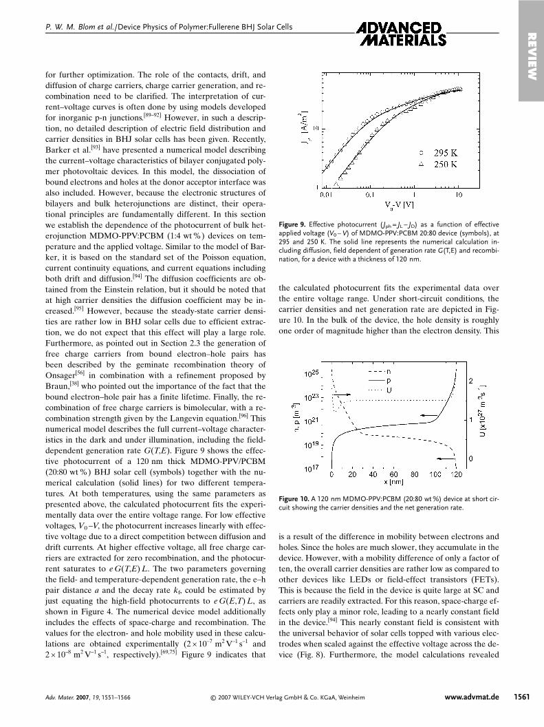
for further optimization. The role of the contacts, drift, anddiffusion of charge carriers, charge carrier generation, and re-combination need to be clarified. The interpretation of cur-rent–voltage curves is often done by using models developedfor inorganic p-n junctions.[89–92] However, in such a descrip-tion, no detailed description of electric field distribution andcarrier densities in BHJ solar cells has been given. Recently,Barker et al.[93] have presented a numerical model describingthe current–voltage characteristics of bilayer conjugated poly-mer photovoltaic devices. In this model, the dissociation ofbound electrons and holes at the donor acceptor interface wasalso included. However, because the electronic structures ofbilayers and bulk heterojunctions are distinct, their opera-tional principles are fundamentally different. In this sectionwe establish the dependence of the photocurrent of bulk het-erojunction MDMO-PPV:PCBM (1:4 wt %) devices on tem-perature and the applied voltage. Similar to the model of Bar-ker, it is based on the standard set of the Poisson equation,current continuity equations, and current equations includingboth drift and diffusion.[94] The diffusion coefficients are ob-tained from the Einstein relation, but it should be noted thatat high carrier densities the diffusion coefficient may be in-creased.[95] However, because the steady-state carrier densi-ties are rather low in BHJ solar cells due to efficient extrac-tion, we do not expect that this effect will play a large role.Furthermore, as pointed out in Section 2.3 the generation offree charge carriers from bound electron–hole pairs hasbeen described by the geminate recombination theory ofOnsager[56] in combination with a refinement proposed byBraun,[38] who pointed out the importance of the fact that thebound electron–hole pair has a finite lifetime. Finally, the re-combination of free charge carriers is bimolecular, with a re-combination strength given by the Langevin equation.[96] Thisnumerical model describes the full current–voltage character-istics in the dark and under illumination, including the field-dependent generation rate G(T,E). Figure 9 shows the effec-tive photocurrent of a 120 nm thick MDMO-PPV/PCBM(20:80 wt %) BHJ solar cell (symbols) together with the nu-merical calculation (solid lines) for two different tempera-tures. At both temperatures, using the same parameters aspresented above, the calculated photocurrent fits the experi-mentally data over the entire voltage range. For low effectivevoltages, V0 –V, the photocurrent increases linearly with effec-tive voltage due to a direct competition between diffusion anddrift currents. At higher effective voltage, all free charge car-riers are extracted for zero recombination, and the photocur-rent saturates to e G(T,E) L. The two parameters governingthe field- and temperature-dependent generation rate, the e–hpair distance a and the decay rate kf, could be estimated byjust equating the high-field photocurrents to e G(E,T) L, asshown in Figure 4. The numerical device model additionallyincludes the effects of space-charge and recombination. Thevalues for the electron- and hole mobility used in these calcu-lations are obtained experimentally (2 × 10⁻⁷ m2 V–1 s–1 and2 × 10–8 m2 V–1 s–1, respectively).[69,75] Figure 9 indicates that
the calculated photocurrent fits the experimental data overthe entire voltage range. Under short-circuit conditions, thecarrier densities and net generation rate are depicted in Fig-ure 10. In the bulk of the device, the hole density is roughlyone order of magnitude higher than the electron density. This
is a result of the difference in mobility between electrons andholes. Since the holes are much slower, they accumulate in thedevice. However, with a mobility difference of only a factor often, the overall carrier densities are rather low as compared toother devices like LEDs or field-effect transistors (FETs).This is because the field in the device is quite large at SC andcarriers are readily extracted. For this reason, space-charge ef-fects only play a minor role, leading to a nearly constant fieldin the device.[94] This nearly constant field is consistent withthe universal behavior of solar cells topped with various elec-trodes when scaled against the effective voltage across the de-vice (Fig. 8). Furthermore, the model calculations revealed
REV
IEWP. W. M. Blom et al./Device Physics of Polymer:Fullerene BHJ Solar Cells
Adv. Mater. 2007, 19, 1551–1566 © 2007 WILEY-VCH Verlag GmbH & Co. KGaA, Weinheim www.advmat.de 1561
Figure 9. Effective photocurrent ( Jph = JL – JD) as a function of effectiveapplied voltage (V0 – V) of MDMO-PPV:PCBM 20:80 device (symbols), at295 and 250 K. The solid line represents the numerical calculation in-cluding diffusion, field dependent of generation rate G(T,E) and recombi-nation, for a device with a thickness of 120 nm.
Figure 10. A 120 nm MDMO-PPV:PCBM (20:80 wt %) device at short cir-cuit showing the carrier densities and the net generation rate.

that at short-circuit conditions only 7.0 % of the free chargecarriers are lost due to bimolecular recombination and subse-quent decay. This low loss of charge carriers is a consequenceof the high field strength, which ensures good charge extrac-tion, resulting in low carrier densities. Since the carrier densi-ties are low, bimolecular recombination is weak and hence therecombination lifetime of the charge carriers is relatively long.Near the contacts, the bimolecular recombination rate R isespecially low since one carrier is dominant (a consequence ofthe ohmic contacts). As a result, the net generation rateU = G – R is highest at the contacts. As stated above, since thehole mobility is lower than the electron mobility, the bulk ofthe device is dominated by holes. Close to the cathode, butnot in the immediate vicinity (about 5 nm), there still exists aconsiderable hole density, but here the electron density alsostrongly increases. Therefore, the rate of bimolecular recom-bination is enhanced close to the cathode, causing a dip in thenet generation rate, as seen in Figure 10.
Furthermore, because of the high field strength, the timeneeded for the charge carriers to exit the device is quite small,and therefore, only few charge carriers are lost. We note thatwe have used a constant generation profile in the model calcu-lations, whereas in BHJ solar cells, optical interference effectsalso play a role.[97] However, we verified that a spatial depen-dence of G does not affect the results presented here, as ex-pected for a solar cell with only minor (bi)molecular recombi-nation losses.
3.2. Effect of the PCBM Weight Fraction on the Solar-CellPerformance
In the MDMO-PPV:PCBM blends, the light is mainly ab-sorbed in the PPV phase, and the role of PCBM is that of theelectron acceptor and electron transport material. However,in order to obtain the maximum device efficiency up to 80wt % PCBM has to be added to the PPV:PCBM mixture.Because the PCBM percolation limit is expected at only17 vol %,[98,99] and the conjugated polymers even shows per-colation at much lower fraction,[100] it is not obvious why it isnecessary to add 80 wt % of a material that hardly contributesto the light absorption to obtain optimum performance. Asshown in Figure 5, the hole mobility when going from 40 to80 wt % PCBM increases by more than two orders of magni-tude from the pure polymer to the blend (5 × 10–11 m2 V–1 s–1
to ca. 1.4 × 10⁻⁸ m2 V–1 s–1). Furthermore, in the saturation re-gime V0 × V > 0.1 V the photocurrent is basically given byJph = e Gmax P(E,T) L. In order to investigate the effect of thePCBM weight fraction on the dissociation efficiency P(E,T),the measured photocurrents have been normalized to theirsaturation value (q Gmax L), as shown in Figure 11 for the 50and 80 wt % PCBM devices. This normalized photocurrentthen reflects the dissociation efficiency in the saturation re-gime for effective voltages V0 × V > 0.1 V. It appears that a de-crease of the PCBM weight fraction from 80 to 50 wt % leads
to a strong reduction of the dissociation efficiency in the rele-vant voltage regime (V0 – V < 0.9 V). The origin of this de-crease in the dissociation efficiency of bound e–h pairs withdecreasing PCBM concentration will be addressed by apply-ing the device model discussed in Section 3.1: For low-mobil-ity semiconductors, recombination of free carriers is given bythe Langevin equation: kR = q <l>/e0<er>,with <er> the spa-tially averaged dielectric constant of MDMO (er = 2.11) andPCBM (er = 3.9) (depending on their volume ratio) and <l>the effective charge carrier mobility of electrons and holes.The parameters in the model which vary with the PCBM frac-tion are kF, er, and kR. Because the average dielectric constantand the charge carrier mobilities are known at each composi-tion (Fig. 5), kF remains the only adjustable parameter in ourcalculation when changing the composition. The dissociationefficiency of the device with 80 wt % PCBM (Fig. 4, solidline) will be used as a reference. From this calculation, a life-time (kF
–1)of typically 2.5 ls was obtained. This long lifetimeis in agreement with absorption spectroscopy measurementswere bound e–h pairs in PPV:PCBM blends can still be de-tected after microseconds and even milliseconds, dependingon temperature.[65,66] However, a quantitative comparison be-tween our calculated kF
–1 of 2.5 ls and these transient absorp-tion measurements is difficult because these measurementsare performed at higher light intensity, charge density, and inthe absence of an electric field. As a next step we systemati-cally calculate P(E,T) for a device with 50 wt % PCBM,changing the input parameters of the 80 wt % device one byone. First, we only adapt the charge carrier mobilities andtake all other parameters as constant. It is observed fromFigure 11 (dotted line) that the decrease of the electron-
REV
IEW
P. W. M. Blom et al./Device Physics of Polymer:Fullerene BHJ Solar Cells
1562 www.advmat.de © 2007 WILEY-VCH Verlag GmbH & Co. KGaA, Weinheim Adv. Mater. 2007, 19, 1551–1566
Figure 11. Experimental photocurrent ( Jph) normalized to its saturationvalue (q Gmax L) as a function of effective applied voltage (V0 – V) for twodifferent MDMO-PPV:PCBM compositions (see legend). The lines repre-sent the calculated dissociation probability of bound e–h pairs (P) at thedonor/acceptor interface as follows: The solid line represents the calcu-lated P that best fits the experimental data, with 80 wt % PCBM used asa reference. The dotted line denotes the calculated P for 50 wt % PCBMwhen only the charge-carrier mobilities have been modified; the dashedline represents the same calculation for the case when both mobility andthe bulk dielectric constant are modified [78].

and hole mobility, although dropping by approximately anorder of magnitude from 80 to 50 wt % PCBM (Fig. 5), isnot solely responsible for the observed decrease in dissocia-tion efficiency. Subsequently, besides the mobility, the changein the spatially averaged dielectric constant <er>, in accor-dance with the change in PPV and PCBM volume ratio,is also taken into account (dashed line). In this case, thecalculated P(E,T) exactly fits the experimental data withouthaving to change any of the other parameters. Thus, the lowerseparation efficiency at 50 wt % PCBM results from thecombination of a decreased charge-carrier mobility andlower dielectric constant, resulting in a stronger e–h bindingenergy. This result demonstrates that the mobilities, maximumgeneration rate, and spatially averaged dielectric constant arethe key parameters which govern the composition depen-dence of the performance of OC1C10-PPV:PCBM based solarcells.
3.3. Formation of Space-Charges in PPV:PCBM BulkHeterojunction Solar Cells
The external photocurrent becomes saturated when allphotogenerated free electrons and holes are extracted fromthe semiconductor. This implies that the mean electron andhole drift lengths we(h) = le(h) se(h) E are equal or longer thanthe specimen thickness L; where le(h) is the charge-carriermobility of electrons (holes), se(h) is the charge-carrier life-time, and E is the internal electric field. In this case, no re-combination occurs and the saturated photocurrent density issimply given by Jph
sat = q G L with G the generation rate offree electrons and holes and q the electric charge. However, ifeither we < L, wh < L, or both are smaller than L, space chargewill form and recombination of free charge-carriers becomessignificant. In other words, recombination becomes importantwhen the transit time of the photogenerated free charge car-riers is longer than their lifetime. Suppose now that the elec-tron–hole pairs are photogenerated uniformly throughout thespecimen and that the charge transport is strongly unbal-anced, meaning that we ≠ wh. In the case that the recombina-tion of free charge-carriers is bimolecular, the free electron-and hole lifetime are equal se = sh. Then, a difference in we
and wh would originate from a difference in charge carriermobility le and lh. In an MDMO-PPV:PCBM blend withlh << le and wh <L, the holes will accumulate to a greater ex-tend in the device than the electrons, which makes the appliedfield nonuniform. As a consequence, the electric field in-creases in the region (L1) near the anode, enhancing the ex-traction of holes. Conversely, in the region near the cathodethe electric field decreases, diminishing the extraction of elec-trons. It is evident that in the region L1 the accumulated holesare not neutralized by an equal density of electrons, which re-sults in a build-up of positive space-charge. Goodman andRose pointed out that that there is a fundamental limit to beexpected for the built-up of space charge in a semiconductorat high light-intensities; The electrostatic limit of hole accu-
mulation is reached when the photocurrent generated in thisregion, Jph = q G L1, is equal to the SCLC[63]
JSCL � 98
e0erlhV1
L1(6)
where e0 er is the dielectric permittivity. By equating q G L1
with Equation 6 it follows that the length of the region L1 inthis space-charge-limited regime is given by
L1 � �9�8e0erlh�8qG�1�4V1�2 (7)
Because V1 ≈ V, the maximum electrostatically allowed photo-current that can be extracted from the device is[63]
Jph � q9e0erlh
8q
� �1�4
G3�4V1�2 (8)
The SCL photocurrent scales with a 3/4 power dependenceon light intensity (Eq. 8), whereas in the absence of space-charge limitations the photocurrent is expected to scale linear-ly with the light intensity. The occurrence of a space-chargelimit in solar cells based on amorphous Si has also been dis-cussed by Crandall[101,102] and more recently by Schiff.[103] Asshown in Section 2.4, in MDMO-PPV:PCBM blends the holemobility in the blend is enhanced by a factor of 400 as com-pare with the pure material, resulting in a much more bal-anced transport. The remaining mobility difference of onlyone order of magnitude is not sufficient to induce SCL photo-currents. This is confirmed by the fact that for MDMO-PPV:PCBM cells the photocurrent closely follows linear be-havior with light intensity.[79,104] As demonstrated in Sec-tion 2.4, when symmetrical substituted PPV is used (such asBEH1BMB3-PPV), the hole mobility in the polymer phase ishardly affected by the presence of PCBM, resulting in an in-creased mobility difference between electrons and holes inthe blend. At room temperature the electron mobility inthe PCBM phase (le = 4 × 10⁻⁷ m2 V–1 s–1) is a factor of 125larger than hole mobility in the BEH1BMB3-PPV phase(lh = 3.2 × 10⁻⁹ m2 V–1 s–1). This difference further increases toa factor of 2000 at T = 210 K because of the difference in acti-vation energy between the electron- (0.18 eV) and hole mo-bility (0.35 eV). Figure 12 shows the experimental Jph as afunction of V0 – V in a 20:80 blend of BEH1BMB3-PPV:PCBMat 210 K for different light-intensities. It is observed that forV0 – V < 0.06 V, the Jph shows linear dependence on voltage.However, above 0.06 V the experimental Jph clearly shows asquare-root dependence on voltage, as is predicted by Equa-tion 8 for very different le and lh values. At larger voltagesJph shows a clear transition to the saturation regime, where itbecomes limited by the field- and temperature dependenceof the generation rate G(E,T). The incident light power(ILP) was varied from 80 mW cm–2 (upper curve) down to6 mW cm–2 using a set of neutral density filters. It appearsfrom Figure 12 that the Jph shows weaker light intensity de-pendence at low voltages in the square-root regime, than athigh voltages in the saturation regime. Figure 13a shows, in adouble logarithmic plot, the experimental Jph taken from Fig-
REV
IEWP. W. M. Blom et al./Device Physics of Polymer:Fullerene BHJ Solar Cells
Adv. Mater. 2007, 19, 1551–1566 © 2007 WILEY-VCH Verlag GmbH & Co. KGaA, Weinheim www.advmat.de 1563

ure 11 as a function of ILP for two different voltages, at V0 –V = 0.1 V in the square-root regime and at V0 – V = 10 V in the
saturation regime. The slope S determined from the linear fit(solid lines) to the experimental data amounts to S = 0.76 inthe square-root part and S = 0.95 in the saturation part at highvoltages. The 1/2 power dependence of Jph on voltage and 3/4dependence on ILP is a strong indication for the occurrenceof a space-charge-limited photocurrent in this materials sys-tem.
Another way to confirm the presence of a SCL photocur-rent is to consider the voltage Vsat at which Jph switches fromthe square-root dependence to the saturation regime. Thistransition occurs when the hole-accumulation region (L1) be-comes equal to the device thickness. In case of a SCL photo-current Vsat scales with the square-root of G. In contrast, inthe absence of a space-charge limit (Eq. 1) the transition volt-age will be independent of light intensity.[57] In Figure 12, thevoltage Vsat at which the transition occurs is determined fromthe crossover point of the square-root dependence and the ex-trapolated saturation part, as indicated by the arrow. In Fig-ure 12, it is already evident that Vsat shows a clear variationwith light intensity. In Figure 13b, Vsat is plotted in doublelogarithmic scale as a function of ILP. A slope S = 0.51 isfound, in agreement with the space-charge-limited prediction.This is further conformation that the photocurrent in 20:80blends of BEH1BMB3-PPV:PCBM devices is truly limited byspace-charge effects. This space-charge-limited photocurrentis the maximum electrostatically allowed current that can begenerated into the external circuit of any solar cell. Further-more, a Jph limited by space charges also has an impact on thepower conversion efficiency of solar cells. Because the Jph isgoverned by a square-root dependence on voltage (Fig. 12),the fill factors of space-charge-limited solar cells are typicallylimited to only ca. 42 %.
4. Outlook
Recently, polymer/fullerene BHJs, based on P3HT as donorand PCBM as acceptor have reached power conversion effi-ciencies of 3.5 %.[96] Although further improvement of devicefabrication has lead to efficiencies of over 4 % for this materi-al combination,[97,98] efficiencies are not yet high enough forcommercial application. As the incident photon to collectedelectron efficiency (IPCE) is already high, up to 70 % at theabsorption maximum of P3HT, it is unclear how much and inwhat way the efficiency of these devices can be further im-proved. As a first approximation Coakley and McGehee pre-dicted that an efficiency of 10 % may be within reach.[106] Intheir calculation it is assumed, among other things, that the fillfactor is equal to unity, and recombination, either geminate orbimolecular, is neglected. Our ability to accurately model thephotocurrent–voltage characteristics of polymer/fullerene so-lar cells enables us to perform a more detailed calculation. Bycombining charge carrier mobility measurements with cur-rent–voltage measurements performed on illuminated solarcells, we quantitatively model the experimental current–volt-age characteristics of P3HT:PCBM solar cells. The obtained
REV
IEW
P. W. M. Blom et al./Device Physics of Polymer:Fullerene BHJ Solar Cells
1564 www.advmat.de © 2007 WILEY-VCH Verlag GmbH & Co. KGaA, Weinheim Adv. Mater. 2007, 19, 1551–1566
Figure 12. Incident light power (ILP) dependence of the photocurrent(Jph) versus the effective voltage (V0 – V) measured at T = 210 K. The sol-id (thick) line represents the calculated Jph from Equation 8 usinglh = 1.2 × 10⁻¹¹ m2 V–1 s–1, er = 2.6, and G ≈ ILP, where ILP was varied from80 to 6 mWcm–2. The arrow indicates the voltage (Vsat) at which Jph
shows the transition to the saturation regime [105].
Figure 13. a) ILP dependence of the photocurrent Jph taken from Fig-ure 11 at an effective voltage of V0 – V = 0.1 V and V0 – V = 10 V (sym-bols). b) Saturation voltage (Vsat) versus ILP as determined for Fig-ure 11. The slope (S) determined from the linear fit (solid lines) to theexperimental data is written on the figure. Reproduced with permissionfrom [105]. Copyright 2005 American Physical Society.

theoretical description of P3HT/PCBM solar cells enables usto investigate the enhancement of the efficiency when a num-ber of solar-cell parameters are varied. We focused on two ef-fects: First the effect of minimizing the energy loss in the elec-tron transfer from donor to acceptor material was found to beof paramount importance; an efficiency of 8.4 % is pre-dicted.[107] This efficiency increase stems from an increase ofVOC. Subsequently, the effect of lowering the polymeric band-gap is studied. Several research groups have put a lot of effortin the synthesis and application of these polymers. At firstglance, a low bandgap polymer seems beneficial. As a resultof enhanced overlap with the solar-cell spectrum the absorp-tion is enhanced, leading to efficiencies larger than 6 %. Sur-prisingly, the model calculations show that once the energyloss in electron transfer is minimized, the best performing so-lar cell comprises a polymer with a bandgap of around 2 eV,clearly not a low bandgap. In the BHJ cells, a lowering of thebandgap is accompanied by a decrease of the open-circuitvoltage, canceling the benefit of an absorption increase. Ulti-mately, with energy levels, bandgaps, and mobilities simulta-neously optimized, single-layer polymer/fullerene solar cellscan reach nearly 11 % efficiency.[107] In order to reach efficien-cies beyond 11 %, tandem cells, consisting of multiple layerseach with their specific absorption maximum and width,should be realized. Although multiple-layer tandem cellsseem incompatible with processing from solution, the firstworking tandem cell based on spin-coated BHJ solar cellswith different absorption spectra has recently been real-ized.[108]
Received: May 19, 2006Revised: September 25, 2006
Published online: May 23, 2007
–[1] D. M. Chapin, C. S. Fuller, G. L. Pearson, J. Appl. Phys. 1954, 25,
676.[2] M. A. Green, K. Emery, D. L. King, S. Igari, W. Warta, Prog. Photo-
voltaics 2005, 13, 49.[3] W. Shockley, H. J. Queisser, J. Appl. Phys. 1961, 32, 510.[4] M. A. Green, Solar Cells: Operating Principles, Technology and Sys-
tem Applications, Prentice-Hall, Englewood Cliffs, NJ, 1982.[5] S. E. Shaheen, R. Radspinner, N. Peyghambarian, G. E. Jabbour,
Appl. Phys. Lett. 2001, 79, 2996.[6] G. Gustafsson, Y. Cao, G. M. Treacy, F. Klavetter, N. Colaneri, A. J.
Heeger, Nature 1992, 357, 477.[7] H. Kallmann, M. Pope, J. Chem. Phys. 1959, 30, 585.[8] S. Barth, H. Bässler, Phys. Rev. Lett. 1997, 79, 4445.[9] P. G. Dacosta, E. M. Conwell, Phys. Rev. B 1993, 48, 1993.
[10] R. N. Marks, J. J. M. Halls, D. D. C. Bradley, R. H. Friend, A. B.Holmes, J. Phys. Condens. Matter 1994, 6, 1379.
[11] V. Choong, Y. Park, Y. Gao, T. Wehrmeister, K. Mullen, B. R. Hsieh,C. W. Tang, Appl. Phys. Lett. 1996, 69, 1492.
[12] J. J. M. Halls, K. Pichler, R. H. Friend, S. C. Moratti, A. B. Holmes,Appl. Phys. Lett. 1996, 68, 3120.
[13] J. J. M. Halls, R. H. Friend, Synth. Met. 1997, 85, 1307.[14] D. E. Markov, E. Amsterdam, P. W. M. Blom, A. B. Sieval, J. C.
Hummelen, J. Phys. Chem. A 2005, 109, 5266.[15] D. E. Markov, C. Tanase, P. W. M. Blom, J. Wildeman, Phys. Rev. B
2005, 72, 045 217.[16] C. W. Tang, Appl. Phys. Lett. 1986, 48, 183.[17] M. Grätzel, Nature 2001, 414, 338.
[18] B. O’Regan, M. Grätzel, Nature 1991, 353, 737.[19] A. K. Jana, J. Photochem. Photobiol. A 2000, 132, 1.[20] P. Peumans, V. Bulovic, S. R. Forrest, Appl. Phys. Lett. 2000, 76,
2650.[21] B. A. Gregg, Chem. Phys. Lett. 1996, 258, 376.[22] M. Granstrom, K. Petritsch, A. C. Arias, A. Lux, M. R. Andersson,
R. H. Friend, Nature 1998, 395, 257.[23] J. J. M. Halls, C. A. Walsh, N. C. Greenham, E. A. Marseglia, R. H.
Friend, S. C. Moratti, A. B. Holmes, Nature 1995, 376, 498.[24] G. Yu, J. Gao, J. C. Hummelen, F. Wudl, A. J. Heeger, Science 1995,
270, 1789.[25] C. J. Brabec, N. S. Sariciftci, J. C. Hummelen, Adv. Funct. Mater.
2001, 11, 15.[26] S. Morita, A. A. Zakhidov, K. Yoshino, Solid State Commun. 1992,
82, 249.[27] N. S. Sariciftci, L. Smilowitz, A. J. Heeger, F. Wudl, Science 1992,
258, 1474.[28] S. E. Shaheen, C. J. Brabec, N. S. Sariciftci, F. Padinger, T. From-
herz, J. C. Hummelen, Appl. Phys. Lett. 2001, 78, 841.[29] D. Chirvase, J. Parisi, J. C. Hummelen, V. Dyakonov, Nanotechnol-
ogy 2004, 15, 1317.[30] Y. Kim, S. A. Choulis, J. Nelson, D. D. C. Bradley, S. Cook, J. R.
Durrant, Appl. Phys. Lett. 2005, 86, 063 502.[31] F. Padinger, R. S. Rittberger, N. S. Sariciftci, Adv. Funct. Mater.
2003, 13, 85.[32] C. J. Brabec, Sol. Energy Mater. Sol. Cells 2004, 83, 273.[33] X. Yang, J. Loos, S. C. Veenstra, W. J. H. Verhees, M. M. Wienk,
J. M. Kroon, M. A. J. Michels, R. A. J. Janssen, Nano Lett. 2005, 5,579.
[34] G. Li, V. Shrotriya, J. Huang, Y. Yao, T. Moriarty, K. Emery, Y. Yang,Nat. Mater. 2005, 4, 864.
[35] W. Ma, C. Yang, X. Gong, K. Lee, A. J. Heeger, Adv. Funct. Mater.2005, 15, 1617.
[36] M. Reyes-Reyes, K. Kim, D. L. Carroll, Appl. Phys. Lett. 2005, 87,083 506.
[37] C. J. Brabec, G. Zerza, G. Cerullo, S. De Silvestri, S. Luzzati, J. C.Hummelen, S. Sariciftci, Chem. Phys. Lett. 2001, 340, 232.
[38] C. L. Braun, J. Chem. Phys. 1984, 80, 4157.[39] T. E. Goliber, J. H. Perlstein, J. Chem. Phys. 1984, 80, 4162.[40] K. Pakbaz, C. H. Lee, A. J. Heeger, T. W. Hagler, D. McBranch,
Synth. Met. 1994, 64, 295.[41] U. Albrecht, H. Bässler, Chem. Phys. 1995, 199, 207.[42] M. Deussen, M. Scheidler, H. Bässler, Synth. Met. 1995, 73, 123.[43] R. Kersting, U. Lemmer, M. Deussen, H. J. Bakker, R. F. Mahrt,
H. Kurz, V. I. Arkhipov, H. Bässler, E. O. Göbel, Phys. Rev. Lett.1994, 73, 1440.
[44] G. Yu, A. J. Heeger, J. Appl. Phys. 1995, 78, 4510.[45] M. Theander, A. Yartsev, D. Zigmantas, V. Sundstrom, W. Mammo,
M. R. Andersson, O. Inganas, Phys. Rev. B 2000, 61, 12 957.[46] A. Haugeneder, M. Neges, C. Kallinger, W. Spirkl, U. Lemmer,
J. Feldmann, U. Scherf, E. Harth, A. Gugel, K. Mullen, Phys. Rev. B1999, 59, 15 346.
[47] T. Stubinger, W. Brutting, J. Appl. Phys. 2001, 90, 3632.[48] T. J. Savenije, J. M. Warman, A. Goossens, Chem. Phys. Lett. 1998,
287, 148.[49] C. Schlebusch, B. Kessler, S. Cramm, W. Eberhardt, Synth. Met.
1996, 77, 151.[50] T. I. Hukka, T. Toivonen, E. Hennebicq, J.-L. Brédas, R. A. J. Jans-
sen, D. Beljonne, Adv. Mater. 2006, 18, 1301[51] Y. Liu, M. A. Summers, S. R. Scully, M. D. McGehee, J. Appl. Phys.
2006, 99, 093 521.[52] P. M. Borsenberger, D. S. Weiss, Organic Photoreceptors for Xero-
graphy, Marcel Dekker, New York 1998.[53] P. M. Borsenberger, L. E. Contois, D. C. Hoesterey, J. Chem. Phys.
1978, 68, 637.[54] P. M. Borsenberger, A. I. Ateya, J. Appl. Phys. 1978, 49, 4035.
REV
IEWP. W. M. Blom et al./Device Physics of Polymer:Fullerene BHJ Solar Cells
Adv. Mater. 2007, 19, 1551–1566 © 2007 WILEY-VCH Verlag GmbH & Co. KGaA, Weinheim www.advmat.de 1565

[55] R. R. Chance, C. L. Braun, J. Chem. Phys. 1976, 64, 3573.[56] L. Onsager, Phys. Rev. 1938, 54, 554.[57] D. Hertel, E. V. Soh, H. Bässler, L. J. Rothberg, Chem. Phys. Lett.
2002, 361, 99.[58] J. Nelson, Phys. Rev. B 2003, 67, 155 209.[59] P. Peumans, S. R. Forrest, Chem. Phys. Lett. 2004, 398, 27.[60] T. Offermans, S. C. J. Meskers, R. A. J. Janssen, Chem. Phys. 2005,
308, 125.[61] V. I. Arkhipov, P. Heremans, H. Bässler, Appl. Phys. Lett. 2003, 82,
4605.[62] J. G. Müller, J. M. Lupton, J. Feldmann, U. Lemmer, M. C. Scharber,
N. S. Sariciftci, C. J. Brabec, U. Scherf, Phys. Rev. B 2005, 72,195 208.
[63] A. M. Goodman, A. Rose, J. Appl. Phys. 1971, 42, 2823.[64] A. F. Nogueira, I. Montanari, J. Nelson, J. R. Durrant, C. Winder,
N. S. Sariciftci, C. Brabec, J. Phys. Chem. B 2003, 107, 1567.[65] I. Montanari, A. F. Nogueira, J. Nelson, J. R. Durrant, C. Winder,
M. A. Loi, N. S. Sariciftci, C. J. Brabec, Appl. Phys. Lett. 2002, 81,3001.
[66] T. Offermans, S. C. J. Mesker, R. A. J. Janssen, J. Chem. Phys. 2003,119, 10 924.
[67] R. Sokel, R. C. Hughes, J. Appl. Phys. 1982, 53, 7414.[68] V. D. Mihailetchi, L. J. A. Koster, J. C. Hummelen, P. W. M. Blom,
Phys. Rev. Lett. 2004, 93, 216 601.[69] V. D. Mihailetchi, J. K. J. van Duren, P. W. M. Blom, J. C. Humme-
len, R. A. J. Janssen, J. M. Kroon, M. T. Rispens, W. J. H. Verhees,M. M. Wienk, Adv. Funct. Mater. 2003, 13, 43.
[70] P. W. M. Blom, M. J. M. de Jong, M. G. van Munster, Phys. Rev. B1997, 55, R656.
[71] W. Geens, S. E. Shaheen, C. J. Brabec, J. Poortmans, N. S. Sariciftci,AIP Conf. Proc. 2000, 544, 516.
[72] C. Tanase, E. J. Meijer, P. W. M. Blom, D. M. de Leeuw, Phys. Rev.Lett. 2003, 91, 216 601.
[73] S. A. Choulis, J. Nelson, Y. Kim, D. Poplavskyy, T. Kreouzis, J. R.Durrant, D. D. C. Bradley, Appl. Phys. Lett. 2003, 83, 3812.
[74] R. Pacios, J. Nelson, D. D. C. Bradley, C. J. Brabec, Appl. Phys. Lett.2003, 83, 4764.
[75] C. Melzer, E. Koop, V. D. Mihailetchi, P. W. M. Blom, Adv. Funct.Mater. 2004, 14, 865.
[76] I. H. Campbell, S. Rubin, T. A. Zawodzinski, J. D. Kress, R. L. Mar-tin, D. L. Smith, N. N. Barashkov, J. P. Ferraris, Phys. Rev. B 1996,54, 14 321.
[77] B. de Boer, A. Hadipour, M. M. Mandoc, T. Van Woudenbergh,P. W. M. Blom, Adv. Mater. 2005, 17, 621.
[78] V. D. Mihailetchi, L. J. A. Koster, P. W. M. Blom, C. Melzer,B. de Boer, J. K. J. van Duren, R. A. J. Janssen, Adv. Funct. Mater.2005, 15, 795.
[79] J. K. J. van Duren, X. Yang, J. Loos, C. W. T. Bulle-Lieuwma, A. B.Sieval, J. C. Hummelen, R. A. J. Janssen, Adv. Funct. Mater. 2004,14, 425.
[80] S. M. Tuladhar, D. Poplavskyy, S. A. Choulis, J. R. Durrant, D. D. C.Bradley, J. Nelson, Adv. Funct. Mater. 2005, 15, 1171.
[81] M. Kemerink, J. K. J. van Duren, P. Jonkheijm, W. F. Pasveer, P. M.Koenraad, R. A. J. Janssen, H. W. M. Salemink, J. H. Wolter, NanoLett. 2003, 3, 1191.
[82] R. Pacios, D. D. C. Bradley, J. Nelson, C. J. Brabec, Synth. Met.2003, 137, 1469.
[83] C. J. Brabec, A. Cravino, D. Meissner, N. S. Sariciftci, T. Fromherz,M. T. Rispens, L. Sanchez, J. C. Hummelen, Adv. Funct. Mater. 2001,11, 374.
[84] V. D. Mihailetchi, P. W. M. Blom, J. C. Hummelen, M. T. Rispens, J.Appl. Phys. 2003, 94, 6849.
[85] H. Frohne, S. E. Shaheen, C. J. Brabec, D. C. Muller, N. S. Sariciftci,K. Meerholz, ChemPhysChem 2002, 3, 795.
[86] M. C. Scharber, D. Mühlbacher, M. Koppe, P. Denk, C. Waldauf,A. J. Heeger, C. Brabec, Adv. Mater. 2006, 18, 789.
[87] C. J. Brabec, S. E. Shaheen, C. Winder, N. S. Sariciftci, Appl. Phys.Lett. 2002, 80, 1288.
[88] V. D. Mihailetchi, L. J. A. Koster, P. W. M. Blom, Appl. Phys. Lett.2004, 85, 970.
[89] E. A. Katz, D. Faiman, S. M. Tuladhar, J. M. Kroon, M. M. Wienk,T. Fromherz, F. Padinger, C. J. Brabec, N. S. Sariciftci, J. Appl. Phys.2001, 90, 5343.
[90] V. Dyakonov, Phys. E 2002, 14, 53.[91] C. J. Brabec, S. E. Shaheen, C. Winder, N. S. Sariciftci, P. Denk,
Appl. Phys. Lett. 2002, 80, 1288.[92] P. Schilinsky, C. Waldauf, J. Hauch, C. J. Brabec, J. Appl. Phys. 2004,
95, 2816.[93] J. A. Barker, C. M. Ramsdale, N. C. Greenham, Phys. Rev. B 2003,
67, 075 205.[94] L. J. A. Koster, E. C. P. Smits, V. D. Mihailetchi, P. W. M. Blom,
Phys. Rev. B 2005, 72, 085 205.[95] Y. Roichman, N. Tessler, Appl. Phys. Lett. 2002, 80, 1948.[96] P. Langevin, Ann. Chim. Phys. 1903, 28, 433.[97] H. Hoppe, N. Arnold, D. Meissner, N. S. Sariciftci, Thin Solid Films
2004, 451, 589.[98] A. Aharony, D. Stauffer, Introduction to Percolation Theory, 2nd ed.,
Taylor and Francis, London 1993.[99] S. Hotta, S. D. D. V. Rughooputh, A. J. Heeger, Synth. Met. 1987,
22, 79.[100] A. J. Heeger, Trends Polym. Sci. 1995, 3, 39.[101] R. S. Crandall, J. Appl. Phys. 1984, 55, 4418[102] R. S. Crandall, J. Appl. Phys. 1983, 54, 7176[103] E. A. Schiff, Sol. Eng. Mater. Sol. Cells 2003, 78, 567.[104] P. Schilinsky, C. Waldauf, C. J. Brabec, Appl. Phys. Lett. 2002, 81,
3885.[105] V. D. Mihailetchi, J. Wildeman, P. W. M. Blom, Phys. Rev. Lett.
2005, 94, 126 602.[106] K. M. Coakley, M. D. McGehee, Chem. Mater. 2004, 16, 4533.[107] L. J. A. Koster, V. D. Mihailetchi, P. W. M. Blom, Appl. Phys. Lett.
2006, 88, 093 511.[108] A. Hadipour, B. de Boer, J. Wildeman, F. B. Kooistra, J. C. Humme-
len, M. G. R. Turbiez, M. M. Wienk, R. A. J. Janssen, P. W. M.Blom, Adv. Funct. Mater. 2006, 16, 1897.
______________________
REV
IEW
P. W. M. Blom et al./Device Physics of Polymer:Fullerene BHJ Solar Cells
1566 www.advmat.de © 2007 WILEY-VCH Verlag GmbH & Co. KGaA, Weinheim Adv. Mater. 2007, 19, 1551–1566