UNIVERSITY OF CALIFORNIA, SAN DIEGO Mostly Digital ADCs...
129
UNIVERSITY OF CALIFORNIA, SAN DIEGO Mostly Digital ADCs for Highly-Scaled CMOS Processes A dissertation submitted in partial satisfaction of the requirements for the degree Doctor of Philosophy in Electrical Engineering (Electronic Circuits and Systems) by Gerard E. Taylor Committee in charge: Professor Ian Galton, Chair Professor James Buckwalter Professor William S. Hodgkiss Professor Lawrence E. Larson Professor Thomas T. Liu 2011
Transcript of UNIVERSITY OF CALIFORNIA, SAN DIEGO Mostly Digital ADCs...
UNIVERSITY OF CALIFORNIA, SAN DIEGO
Mostly Digital ADCs for Highly-Scaled CMOS Processes
A dissertation submitted in partial satisfaction of the requirements for the degree
Doctor of Philosophy
in
Electrical Engineering (Electronic Circuits and Systems)
by
Gerard E. Taylor
Committee in charge:
Professor Ian Galton, Chair
Professor James Buckwalter
Professor William S. Hodgkiss
Professor Lawrence E. Larson
Professor Thomas T. Liu
2011

Copyright
Gerard E. Taylor, 2011
All rights reserved.

The dissertation of Gerard E. Taylor is approved, and it is acceptable in
quality and form for publication on microfilm and electronically:
Chair
University of California, San Diego
2011

DEDICATION
To my wife Kathleen, who supported and encouraged me thoughout this long
and difficult undertaking .

TABLE OF CONTENTS
Signature Page ................................................................................................................................iii
Dedication ...................................................................................................................................... iv
Table of Contents............................................................................................................................. v
List of Figures ...............................................................................................................................vii
List of Tables .................................................................................................................................. ix
Acknowledgements ......................................................................................................................... x
Vita ................................................................................................................................................xii
Abstract of the Dissertation ..........................................................................................................xiii
I. Introduction................................................................................................................................ 1
I.A. Motivation for the New ∆Σ Modulator Architecture ..................................................... 1
I.B. VCO-Based ∆Σ Modulator............................................................................................ 2
I.C. Dissertation Organization............................................................................................. 3
II. VCO-Based ∆Σ Modulator Overview ..................................................................................... 5
II.A. Ideal Operation............................................................................................................. 5
II.B. A ring VCO Implementation.......................................................................................... 7
II.C. The Nonlinearity Problem............................................................................................. 9
III. Signal Processing Details ...................................................................................................... 12
III.A. Digital Background Calibration ................................................................................. 12
III.B. Pseudo-Differential Topology...................................................................................... 17
III.C. Self-Cancelling Dither Technique ............................................................................... 19
III.D. The Implemented ∆Σ Modulator Architecture............................................................. 21
III.E. Quantization Noise, No-overload Range, and the Number of Ring Elements............. 22
IV. Circuit Details ........................................................................................................................ 25
IV.A. ICRO, Ring Sampler, and Phase Decoder................................................................... 25
IV.B. V/I converter ............................................................................................................... 26
IV.C. Dither DACs................................................................................................................ 29
IV.D. Nonlinearity Correction Block .................................................................................... 30
IV.E. Circuit Noise Sources.................................................................................................. 31
V. First Prototype IC ................................................................................................................... 33
V.A. Measurement Results .................................................................................................. 33
V.B. Conclusions................................................................................................................. 37
VI. Architectural Enhancements ................................................................................................ 40
VI.A. Quantization Noise Reduction in a VCO-Based ADC................................................. 40
VI.B. Quantization Noise Reduction by Extended No-Overload Range ............................... 42
VI.C. Dither .......................................................................................................................... 48
VI.D. Low Voltage V/I Converter.......................................................................................... 55
VI.E. Digital Background Calibration ................................................................................. 59
VII. Circuit Level Enhancements............................................................................................... 66
VII.A. Achieving Theoretical Maximum SQNR...................................................................... 66
VII.B. Signal Path AC Nonlinearity....................................................................................... 67
VII.C. Ring Sampler Hysteresis Problem............................................................................... 69
VII.D. Process Scaling ........................................................................................................... 70
VIII. Second Prototype IC .......................................................................................................... 72
VIII.A. Measurement Results .................................................................................................. 72
VIII.B. Conclusions................................................................................................................. 77
IX. Third Prototype IC................................................................................................................ 80
IX.A. Measurement Results .................................................................................................. 80
IX.B. Conclusions................................................................................................................. 83
X. CONCLUSIONS..................................................................................................................... 84
Figures ................................................................................................................................ 85
Tables .............................................................................................................................. 110
References .............................................................................................................................. 113
LIST OF FIGURES
Figure 1: Equivalent systems: (a) a generic VCO-based ∆Σ modulator, (b) the cascade of a
continuous-time lowpass filter, sampler, quantizer, and digital differentiator, and (c)
the cascade of a continuous-time lowpass filter, sampler and first-order ∆Σ
modulator......................................................................................................................................85 Figure 2: Example of a ring VCO and phase-to-digital converter .........................................................86 Figure 3: The prototype IC’s on-chip calibration unit shown with a single VCO-based ∆Σ
modulator signal path for simplicity. .........................................................................................86 Figure 4: A pseudo-differential signal path and the calibration unit. ....................................................87 Figure 5: High-level block diagram of the implemented VCO-based ∆Σ modulator............................87 Figure 6: Example of the signal-dependent non-uniform quantization problem..................................88 Figure 7: Example of the solution used to solve the signal-dependent non-uniform
quantization problem. .................................................................................................................88 Figure 8: Circuit diagrams of the V/I converter and ICRO....................................................................89 Figure 9: The dither DAC swapping technique which causes the PSD of the error component
in the ∆Σ modulator output arising from mismatches between the dither DACs to
have a first-order highpass shape. ..............................................................................................90 Figure 10: Nonlinearity correction block details. ....................................................................................90 Figure 11: Die photograph. ........................................................................................................................91 Figure 12: Representative measured PSD plots of the first prototype IC ∆Σ modulator output
before and after digital background calibration (initial convergence time of digital
calibration unit is 233ms). ...........................................................................................................92 Figure 13: Plots of the first prototype IC’s measured output PSD for a two-tone out-of-band
input signal (top) and inter-modulation distortion (bottom) for the ∆Σ modulator run
with fs = 1.152GHz. The top and bottom plots indicate how the inter-modulation
values were measured. .................................................................................................................93 Figure 14: Plots of the fist prototype IC’s measured SNR and SNDR for an 18 MHz signal
band (top) bandwidth 9MHz signal-band (bottom) for the ∆Σ modulator run with fs =
1.152GHz. .....................................................................................................................................94 Figure 15: Representative measured PSD plots of the first prototype IC ∆Σ∆Σ∆Σ∆Σ modulator output
with and without dither...............................................................................................................95 Figure 16: Circuit diagrams of various ICROs: (a) 15-element ICRO used in the first
prototype IC, (b) example 7-element ICRO, (c) dual, 7-element injection-locked
ICRO used in the second prototype IC ......................................................................................96 Figure 17: Over-Range Correction block (ORC): (a) signal path with the addition of over-
range correction, (b) details of the ORC block, (c) overflow logic truth table, (d)
example overload waveform before ORC, (e) example waveform after ORC, (f)
example waveform after ORC demonstrating clipping behavior. ...........................................97 Figure 18: High-level block diagram of two VCO-based ∆Σ∆Σ∆Σ∆Σ modulators: (a) single pseudo-
differential modulator ADC with dither injected as a common-mode signal, (b) dual
pseudo-differential modulator ADC with dither injected as a differential signal. .................98 Figure 19: V/I circuit diagrams: (a) first prototype IC V/I converter, (b) new open-loop V/I
converter.......................................................................................................................................99 Figure 20: The second prototype IC’s on-chip calibration unit shown with a single VCO-based
∆Σ∆Σ∆Σ∆Σ modulator signal path for simplicity ..................................................................................100 Figure 21: Calibration unit details: (a) example transformer-based input circuit for the ADC,
(b) example active-circuit based input circuit for the ADC, (c) detailed circuit
diagram of the calibration DAC and signal path replica. ......................................................101 Figure 22: Circuit diagrams of the ring sampler D-type flip-flops, (a) transmission-gate flip-
flop used in the first prototype that produces data-dependent hysteresis, (b) non-
transmission-gate flip-flop that is largely hysteresis free. ......................................................102
Figure 23: Die photograph of second prototype IC ...............................................................................103 Figure 24: Representative measured PSD plots of the second prototype IC ∆Σ∆Σ∆Σ∆Σ modulator
output before and after digital background calibration.........................................................104 Figure 25: Plots of the second prototype IC’s measured output PSD for a single-tone input
signal (top) and the harmonic distortion values (bottom) for the ∆Σ∆Σ∆Σ∆Σ modulator run
with fS=2.4GHz. The top and bottom plots indicate how the harmonic distortion
values were measured. ...............................................................................................................105 Figure 26: Plots of the second prototype IC’s measured SNR and SNDR for a 37.5MHz signal
bandwidth (top) and an 18MHz signal bandwidth (bottom) for the second prototype
∆Σ∆Σ∆Σ∆Σ modulator run with fS=2.4GHz. ..........................................................................................106 Figure 27: Representative measured PSD plots of the third prototype IC ∆Σ∆Σ∆Σ∆Σ modulator output
before and after digital background calibration .....................................................................107 Figure 28: Plots of the third prototype IC’s measured output PSD for a two-tone out-of-band
input signal (top) and inter-modulation distortion (bottom) for the ∆Σ modulator run
with fs = 1.6GHz. The top and bottom plots indicate how the inter-modulation values
were measured............................................................................................................................108 Figure 29: Plots of the third prototype IC’s measured SNR and SNDR for a 25MHz signal
bandwidth (top) and an 12.5MHz signal bandwidth (bottom) for the third prototype
∆Σ∆Σ∆Σ∆Σ modulator run with fS=1.6GHz. ..........................................................................................109

LIST OF TABLES
Table 1: Performance table and comparison of first prototype IC to prior state-of-the-art
∆Σ modulators............................................................................................................................ 110 Table 2: Performance table and comparison of second prototype IC to prior state-of-the-art
∆Σ modulators............................................................................................................................ 111 Table 3: Performance table and comparison of third prototype IC fabricated in 65nm LP
process to first IC fabricated in 65nm G+ process.................................................................. 112

ACKNOWLEDGEMENTS
First of all, I would like to thank my advisor Professor Ian Galton. If I had not
met him, I would never have considered doing a Ph.D. He was instrumental in finding a
way to make this PhD possible and I would never have made it through to the end with-
out his encouragement and his faith in me throughout this project. His guidance, posi-
tive attitude, and daily consultations were crucial to the success of this project.
I would like to thank all my lab colleagues for their friendship and support. They
were always there for me when I needed help with something. Plus, they were always a
fun distraction when we needed a break.
I want to thank Analog Devices, and Allen Barlow in particular, for their unending
support of me and this project. Their support was extremely generous and I will forever
be in their debt and be full of gratitude. I also want to thank Tom Pilling of Analog De-
vices for his help with the layout for this project. He suffered greatly during the first pro-
totype IC tapeout and generously gave his free time and went above and beyond the call
of duty to make the first prototype IC meet the shuttle deadline.
Finally, and most importantly, I want to thank my wife Kathleen for her uncondi-
tional and unwavering support though out this endeavor. She undoubtedly suffered the
greatest hardship throughout this process, having to raise four small children alone much
of the time. She was always there for me and was a constant source of encouragement
and faith.
Chapters I through V are largely taken from a paper entitled “A Mostly-Digital
Variable-Rate Continuous-Time Delta-Sigma Modulator ADC” published in the IEEE
Journal of Solid-State Circuits, volume 45, number 12, pages 2634-2646, December
2010. The dissertation author is the primary investigator and author of this paper. Pro-
fessor Ian Galton supervised the research which forms the basis for this paper.
VITA
1990 Bachelor of Science, University of California, Los Angeles
1992 Master of Science, University of California, Los Angeles
1992 – 1998 Design Engineer and Manager, Micro Linear Corp.
1998 – 2001 Design Engineer and Manager, Antrim Design Systems
2001 – 2006 Design Engineer and Director, Vativ Technologies
2006 – 2011 Design Engineer, Analog Devices Inc.
2011 Doctor of Philosophy, University of California, San Diego
ABSTRACT OF THE DISSERTATION
Mostly Digital ADCs for Highly-Scaled CMOS Processes
by
Gerard E. Taylor
Doctor of Philosophy in Electrical Engineering (Electronic Circuits and Systems)
University of California, San Diego, 2011
Professor Ian Galton, Chair
Delta-Sigma (∆Σ) modulator ADCs are used extensively in applications where the
analog signal bandwidth is narrow compared to practical ADC sample-rates because
these ADCs are very efficient and the oversampling relaxes the analog filtering require-
ments prior to digitization. Conventional continuous-time ∆Σ modulator ADCs require

high a ccuracy building block including low-leakage analog integrators, high-linearity
feedback DACs, high-accuracy reference voltages, high-speed comparators, and low-
jitter clocks. Unfortunately, as process technologies scale and supply voltages are re-
duced it becomes increasingly difficult to build these circuits. Fortunately however,
highly scaled CMOS processes offer very fast, very dense and very low-power digital
logic gates.
This dissertation presents continuous-time ∆Σ modulator ADCs that consist
mostly of digital logic gates. The ADCs are a voltage-controlled ring oscillator based
design with new digital background calibration and self-cancelling dither techniques ap-
plied to enhance performance. Unlike conventional delta-sigma modulators, they do not
contain analog integrators, feedback DACs, comparators, or reference voltages, and do
not require a low-jitter clock. Therefore, they use less area than comparable conventional
delta-sigma modulators, and the architecture is well-suited to IC processes optimized for
fast digital circuitry.
Prototype ICs were fabricated in both the 65nm LP and 65nm G+ CMOS proc-
esses. The performance of the prototype ICs is comparable to the state-of-the-art in
terms of power figure-of-merit but this new architecture uses significantly less circuit
area.
1
I. INTRODUCTION
I.A. Motivation for the New ∆Σ∆Σ∆Σ∆Σ Modulator Architecture
In many analog-to-digital converter (ADC) applications such as wireless receiver
handsets, the bandwidth of the analog signal of interest is narrow relative to practical
ADC sample-rates. Delta-sigma (∆Σ) modulator ADCs are used almost exclusively in
such applications because they offer exceptional efficiency and relax the analog filtering
required prior to digitization [1]. Continuous-time ∆Σ modulator ADCs with clock rates
above several hundred MHz have been shown to be particularly good in these respects
[2],[3],[4],[5].
Unfortunately, conventional analog ∆Σ modulators present significant design
challenges when implemented in highly-scaled CMOS IC technology optimized for digi-
tal circuitry. They require analog comparators, high-accuracy analog integrators, high-
linearity feedback DACs, and low-noise, low-impedance reference voltage sources. Con-
tinuous-time ∆Σ modulators with continuous-time feedback DACs additionally require
low-jitter clock sources. These circuit blocks are increasingly difficult to design as
CMOS technology is scaled below the 90 nm node because the scaling tends to worsen
supply voltage limitations, device leakage, device nonlinearity, signal isolation, and 1/f
noise.
2
I.B. VCO-Based ∆Σ∆Σ∆Σ∆Σ Modulator
An alternate type of ∆Σ modulator which does not require the above-mentioned
analog blocks consists of a voltage-controlled ring oscillator (ring VCO) with its inverters
sampled at the desired output sample-rate followed by digital circuitry [6],[7],[8],[9],
[10], [11]. Although the ring VCO inevitably introduces severe nonlinearity, the structure
otherwise has the same functionality as a first-order continuous-time ∆Σ modulator. Un-
fortunately, the nonlinearity problem and the high spurious tone content of first-order ∆Σ
modulator quantization noise has limited the deployment of such VCO-based ∆Σ modula-
tors to date. The only previously published method of circumventing these problems is to
use the VCO-based ∆Σ modulator as the last stage of an otherwise conventional analog
∆Σ modulator, but this solution requires all the high-performance analog blocks of a con-
ventional analog ∆Σ modulator except comparators [12].
This work presents a VCO-based ∆Σ modulator that incorporates two new tech-
niques with which it avoids these problems: digital background correction of VCO
nonlinearity, and self-cancelling dither [13]. The digital background calibration technique
is an extension of a technique originally used to correct nonlinear distortion in pipelined
ADCs [14], [15]. The self-cancelling dither technique eliminates the spurious tone prob-
lem by adding dither sequences prior to quantization and then cancelling them in the digi-
tal domain. Additionally, the ∆Σ modulator uses a new digital calibration technique that
enables reconfigurability by automatically retuning the VCO’s center frequency when-
ever the ∆Σ modulator’s sample-rate is changed.
3
The new techniques enable the ∆Σ modulator to achieve high-performance data
conversion without analog integrators, feedback DACs, comparators, reference voltages,
or a low-jitter clock. Therefore, it uses less area than comparable conventional analog ∆Σ
modulators, and the architecture is well-suited to highly-scaled CMOS technology opti-
mized for fast digital circuitry.
I.C. Dissertation Organization
The dissertation presents the theory, analysis and circuit results for three different
versions of a VCO-based ∆Σ modulator. The dissertation consists of ten chapters.
Chapter II describes the VCO-based ∆Σ modulator concept, and quantifies the
VCO nonlinearity problem. Chapter III presents the signal processing enhancements in-
cluding digital background calibration, pseudo-differential topology, and self-cancelling
dither technique. Chapter IV presents the ∆Σ modulator’s key circuits. Chapter V pre-
sents measurement results for the first prototype IC, fabricated in the 65nm LP process,
and draws conclusions about the ADCs performance and shortcomings. Chapter VI de-
scribes a number of architectural enhancements to improve the ∆Σ modulator’s perform-
ance and usability. Chapter VII describes a number of circuit-level enhancements to
boost the ∆Σ modulator’s performance. Chapter VIII presents measurement results for a
second prototype IC, fabricated in the 65nm G+ process, which incorporates all of the
enhancements described in Chapters VI and VII. Chapter IX presents measurement re-
sults for a third prototype IC, also fabricated in the 65nm G+ process, which is similar to
the first prototype IC and is intended to prove the benefits of process scaling for the

4
VCO-based ∆Σ modulator architecture. And chapter X presents conclusions of this re-
search.
Chapter I is largely taken from Section I of the paper entitled “A Mostly-Digital
Variable-Rate Continuous-Time Delta-Sigma Modulator ADC” published in the IEEE
Journal of Solid-State Circuits, volume 45, number 12, pages 2634-2646, December
2010. The dissertation author is the primary investigator and author of this paper. Pro-
fessor Ian Galton supervised the research which forms the basis for this paper
.
5
II. VCO-BASED ∆Σ MODULATOR OVERVIEW
II.A. Ideal Operation
An idealized VCO-based ∆Σ modulator with a continuous-time input voltage, v(t),
and a digital output signal, y[n], is shown in Figure 1(a). It consists of a VCO, a phase-to-
digital converter, and a digital differentiator block with a transfer function of 1−z−1
. Ide-
ally, the instantaneous frequency of the VCO is
( ) ( )2
VCOVCO s
Kf t f v t
π= + (1)
where fs is the center frequency of the VCO in Hz, and KVCO is the VCO gain in radians
per second per volt. The phase-to-digital converter quantizes the VCO phase, i.e., the
time integral of the instantaneous frequency, and generates output samples of the result at
times nTs, n = 0, 1, 2, …, where Ts = 1/fs.
In a practical implementation the phase-to-digital converter would typically gen-
erate its output samples modulo one-cycle. It can be verified that provided
( )0.5 1.5s VCO sf f t f< < (2)
for all t and another modulo one-cycle operation is performed after the digital differenti-
ator, then the digital output signal is not affected by the modulo operations. Therefore, the

6
modulo operations are not considered in the following to simplify the explanation.
Aside from an integer multiple of a cycle (which ultimately has no effect on y[n]
because of the modulo operations), the nth output sample of the phase to digital converter
in radians is a quantized version of
( )0
[ ]snT
VCOn K v dφ τ τ= ∫ . (3)
Equivalently, (3) can be written as
1
[ ] [ ]n
k
n kφ ω=
=∑ , (4)
where
( 1)
[ ] ( )s
s
nT
VCOn T
n K v dω τ τ−
= ∫ . (5)
It follows that ω[n] could have been obtained by passing v(t) through a lowpass continu-
ous-time filter with transfer function
( ) ( )sinsj T f s
c VCO
T fH f K e
f
π ππ
−= (6)
and sampling the output of the filter at a rate of fs.
The system of Figure 1(b) is, therefore, equivalent to that of Figure 1(a). It obtains
ω[n] by sampling a filtered version of the input signal as described above and implements
(4) as a discrete-time integrator. The discrete-time integrator is followed by the same
quantizer and digital differentiator as in Figure 1(a) to obtain y[n].

7
Given that the discrete-time integrator and differentiator both have integer-valued
impulse responses, it can be verified that the system of Figure 1(b), and, hence, the sys-
tem of Figure 1(a), is equivalent to the system of Figure 1(c) [16]. Thus, the VCO-based
∆Σ modulator is equivalent to a conventional first-order continuous-time ∆Σ modulator,
so it can be analyzed by applying well-known properties of the first-order ∆Σ modulator
to the system of Figure 1(c) [1]. In particular
[ ] [ ] [ ]y n n e nω ∆Σ= + , (7)
where e∆Σ[n] is first-order highpass shaped quantization noise.
II.B. A ring VCO Implementation
A practical topology with which to implement the VCO and phase-to-digital con-
verter is shown in Figure 2. In this example, the VCO is a ring oscillator that consists of
five inverters, each with a transition delay that depends on the VCO input voltage, v(t).
The ring sampler consists of five flip-flops clocked at a rate of fs, where the D input of
each flip-flop is driven by the output of one of the VCO’s inverters. At each rising edge
of the clock signal, i.e., at times nTs, the output of each flip-flop is set high if the corre-
sponding VCO inverter output signal at that time is above the flip-flop’s digital logic
threshold of approximately half the supply voltage, and is set low otherwise.
A well known property of ring oscillators is that at any given time during oscilla-
tion, exactly one of the VCO’s inverters is in a state of either positive transition or nega-
tive transition, i.e., a state in which the inverter’s input and output are both below or both

8
above the digital logic thresholds of the flip-flops to which they are connected, respec-
tively. For example, suppose Inverter 1 in Figure 2 enters positive transition at time t0.
The inverter remains in positive transition until a time t1 at which its output rises above
the digital logic threshold of the flip-flop to which it is connected. At this same instant,
Inverter 2 enters negative transition. This process continues in a clockwise direction
around the VCO such that Inverter (1+(i mod 5)) is in positive transition from time ti to
time ti+1 if i is even, and is in negative transition from time ti to time ti+1 if i is odd for i =
0, 1, 2, …, where ti+1 > ti.
Therefore, each inverter goes once into positive transition and once into negative
transition during each VCO period, and there are only 10 possible 5-bit values that the
ring sampler can generate regardless of when it is sampled. The phase decoder maps each
of the 10 values into a phase number, [ ]nφɶ , in the range {0, 1, 2, …, 9} (the correspond-
ing phase in radians is given by 2 [ ] /10nπφɶ ). Since each phase number corresponds to
one of the inverters being in a state of transition and there are 10 such states per VCO pe-
riod, [ ]nφɶ represents the phase of the VCO modulo one-cycle quantized to the nearest
10th of a cycle as depicted in Figure 2.
Ideally, the VCO inverters are such that the ith transition delay is given by
( )1 1
1,
10i i s d i i
t t T K v t t+ +− = − . (8)
where
9
( ) 1
1
1
1, ( )
i
i
t
i it
i i
v t t v t dtt t
+
++
=− ∫ (9)
is the average value of v(t) over the time interval from ti to ti+1. This time interval repre-
sents a 10th of the corresponding VCO cycle as described above, so (8) implies that the
VCO’s average frequency during this time interval, i.e.,
1
1
1( )
i
i
t
VCOt
i i
f t dtt t
+
+ − ∫ (10)
where fVCO(t) is the VCO’s instantaneous frequency at time t, can be written as
( )1
1
10i i
t t+ −. (11)
Substituting (8) into (11) and expanding the result as a power series yields
( )1
1
01
1 1( ) , .
i
i
nt
dVCO i i
tni i s s
Kf t dt v t t
t t T T
+∞
+=+
= −
∑∫ (12)
Provided that v(t) does not change significantly between ti and ti+1, it follows that the
VCO can be modeled as having an instantaneous frequency given by
2
1( ) ( ) ( )
2 2
n
VCO s VCOVCO s
ns
K T Kf t f v t v t
Tπ π
∞
=
= + +
∑ (13)
where KVCO ≡ 2πKd /Ts2.
II.C. The Nonlinearity Problem
A comparison of the instantaneous frequency of the ring VCO given by (13) to the
10
ideal instantaneous frequency given by (1) indicates that the ring VCO introduces nonlin-
ear distortion. Applying the reasoning of Section II.A leads to the conclusion that the dis-
tortion causes the input to the first-order ∆Σ modulator in the equivalent system of Figure
1(c) to be
( 1)
2
2[ ] ( )
2
s
s
inT
s VCO
n Tis
T Kn v d
T
πω τ τπ
∞
−=
+
∑∫ (14)
instead of just ω[n]. It follows from (5) and (7) that provided v(t) does not change sig-
nificantly over each sample interval, the output of the ∆Σ modulator is
( )2
[ ] [ ] [ ] [ ]i
i
i
y n n e n nω α ω∞
∆Σ=
= + +∑ , (15)
where
11
2
i
iα
π
− ≅
, (16)
for i = 2, 3, …, are nonlinear distortion coefficients.
It should be stressed that the nonlinearity is not the result of non-ideal circuit be-
havior. It is a systematic nonlinearity that occurs even with ideal circuit behavior. The
problem is that the VCO’s period changes linearly with v(t), but to eliminate the nonlin-
ear terms in (14) it would be necessary for the VCO’s frequency to change linearity with
v(t). It is the reciprocal relationship between VCO’s period and frequency that give rise to
the nonlinear terms in (14). Of course, in practice the relationship between the inverter
delays and the input voltage is not perfectly linear as assumed by (8). While this intro-
11
duces additional significant nonlinearity it tends to be less severe than the reciprocal
nonlinearity described above.
Transistor-level simulations of the VCO-based ∆Σ modulator described above
with the 15-element VCO designed for the IC prototype presented in this paper support
these findings and demonstrate the severity of the problem. For instance, the output of the
simulated ∆Σ modulator with fs = 1.152 GHz and a full-scale 250 KHz sinusoidal input
signal has second, third, and fourth harmonics at −26 dBc, −47 dBc, and −64 dBc, re-
spectively. When the simulated output sequence is corrected in the digital domain to can-
cel just the second-, third-, and fourth-order distortion terms using the techniques pre-
sented in the next chapter, the largest harmonic in the corrected sequence is less than −90
dBc1. This suggests that for the target specifications of the IC prototype presented in this
paper it is only necessary to cancel the second-, third-, and fourth-order distortion terms.
Chapter II is largely taken from Section II of a paper entitled “A Mostly-Digital
Variable-Rate Continuous-Time Delta-Sigma Modulator ADC” published in the IEEE
Journal of Solid-State Circuits, volume 45, number 12, pages 2634-2646, December
2010. The dissertation author is the primary investigator and author of this paper. Pro-
fessor Ian Galton supervised the research which forms the basis for this paper.
1 It can be verified that the technique used to cancel the α3 term in (15) introduces a fifth-order term that
happens to largely cancel the α5 term in (15) as a side-effect.

12
III. SIGNAL PROCESSING DETAILS
The prototype IC contains two identical ∆Σ modulators that each incorporate four
of the basic VCO-based ∆Σ modulators described above as separate signal paths. They
also contain additional components that implement the digital background calibration and
self-cancelling dither techniques. The signal processing details of the ∆Σ modulator de-
sign and the reasons for using four such signal paths in a single ∆Σ modulator are pre-
sented in this chapter.
III.A. Digital Background Calibration
Two types of digital background calibration are implemented in each ∆Σ modula-
tor: 1) digital background cancellation of VCO-induced second-order and third-order dis-
tortion, and 2) digital background tuning of the VCO’s center frequency to the ∆Σ modu-
lator’s sample rate, fs. The former in combination with a pseudo-differential architecture
to be explained shortly addresses the nonlinearity problem described in the previous
chapter. The latter centers the input range of the ∆Σ modulator about the midscale input
voltage. This maximizes the dynamic range, and enables reconfigurability by automati-
cally retuning the VCO’s center frequency whenever fs is changed.
Figure 3 shows a block diagram of a single VCO-based ∆Σ modulator signal path
and the on-chip calibration unit shared by all the signal paths in both ∆Σ modulators. The
signal path is similar to the VCO-based ∆Σ modulator described in Section II.B, except

13
that its VCO is implemented as a voltage-to-current (V/I) converter followed by a 15-
element current-controlled ring oscillator (ICRO), and it contains a nonlinearity correc-
tion block that cancels the distortion terms in (15). The calibration unit measures the
VCO center frequency and nonlinear distortion of a signal path replica, and generates
digital data used by the actual signal path to properly tune the VCO’s center frequency
and cancel nonlinear distortion. The calibration unit operates continuously in background,
and periodically updates its output data with new measurement results.
The calibration unit’s signal path replica is identical to the actual signal path ex-
cept that it does not have a nonlinearity correction block, its differential input voltage is
zero (i.e., it has a constant, midscale input signal), and a four-level current steering fs/64-
rate DAC adds a calibration sequence to the input of its ICRO. The calibration sequence
is t1[n]+t2[n]+t3[n] where the ti[n] sequences are 2-level, independent, zero-mean, pseudo-
random sequences.
III.A.1 VCO Center Frequency Calibration
The calibration unit’s VCO center frequency calculator block adds each succes-
sive set of 228
output samples from the signal path replica and scales the result by a con-
stant, K, to create an fs/228
-rate digital sequence given by
[ ] [ ]1
0
P
i
I m K r mP i−
=
∆ = +∑ (17)
where P = 228
, and r[n] is the output of the signal path replica. The eight most significant
bits (MSBs) of this sequence are used to adjust the output current of the V/I converter in
14
the signal path replica. This forms a negative feedback loop with a bandwidth that de-
pends on K. The feedback drives the VCO’s output frequency to the point at which r[n]
has zero mean. The frequency to which the VCO converges is fs, because the VCO’s input
voltage is zero and the calibration sequence has a mean of zero. The V/I converter in the
signal path is also adjusted by the ∆I[m] sequence. To the extent that the signal path and
signal path replica match, this causes the signal path’s VCO to have a frequency very
close to fs when v(t) = 0.
The choice of K is not critical because settling error in the loop introduces only as
a small common-mode error in the ∆Σ modulator. In the prototype IC, K was chosen to
achieve one-step settling.
III.A.2 Nonlinearity Correction
The nonlinearity correction block in the signal path is a high-speed look-up table
with mapping data updated periodically by the nonlinearity coefficient calculator block of
the calibration unit. The look-up table maps each 5-bit input sample, y[n], into an output
sample, y[n]|corrected, such that
( ) ( )( )32 22
2 3 2 2corrected[ ] [ ] [ ] ( 2 ) [ ] [ ]y n y n y n y n y nα α α α= − − − −ɶ ɶ ɶ ɶ (18)
where 2αɶ , and 3αɶ are measurements of the α2 and α3 coefficients in (15), respectively. It
can be verified that if i i
α α=ɶ , for i = 2 and 3, then y[n]|corrected does not contain any VCO-
induced second-order or third-order distortion terms.

15
Applying (18) to obtain y[n]|corrected also has some side effects. A positive side ef-
fect is that it adds a fifth-order term that happens to nearly cancel the portion of the fifth-
order distortion corresponding to α5 given by (16). Negative side effects are that it adds
higher-order distortion terms and cross terms that include (e∆Σ[n])i for i = 2, 3, 4, 5, and 6.
Fortunately, these terms are sufficiently small that they do not significantly degrade the
simulated or measured performance of the ∆Σ modulator. The cross terms containing
(e∆Σ[n])i fold some of the ∆Σ quantization noise into the signal band but the folded noise
is well below the overall signal band noise floor of the ∆Σ modulator. This is because the
15-element ring oscillator quantizes each phase estimate to within 1/30 of a VCO period
so e∆Σ[n] is small relative to ω[n]. Had a VCO with fewer ring elements been used, the
folding of ∆Σ quantization noise into the signal band would not necessarily have been
negligible.
III.A.3 Nonlinearity Coefficient Measurement
The purpose of the nonlinearity coefficient calculator block is to generate the 30
values of (18) that correspond to the 30 possible values of y[n]. While using the values of
α2 and α3 given by (16) for 2αɶ and 3αɶ , respectively, in (18) would result in cancellation
of much of the nonlinear distortion, it would not address nonlinear distortion arising from
non-ideal circuit behavior, and simulations suggest that this would limit the ADC’s sig-
nal-to-noise-and-distortion-ratio (SNDR) to between 60 dB and 65 dB.
Therefore, the calibration unit continuously measures 2α and 3α by correlating
the output of the signal path replica against the three 2-level sequences: t1[n], t1[n]×t2[n],
16
and t1[n]×t2[n]×t3[n], to obtain the three fs/228
-rate sequences given by
[ ] [ ] [ ]1
1 1
0
1 P
i
m r mP i t mP iP
γ−
=
= + +∑ , (19)
[ ] [ ] [ ] [ ]1
2 1 2
0
1 P
i
m r mP i t mP i t mP iP
γ−
=
= + + +∑ , (20)
and
[ ] [ ] [ ] [ ] [ ]1
3 1 2 3
0
1 P
i
m r mP i t mP i t mP i t mP iP
γ−
== + + + +∑ . (21)
where P = 228
. It can be verified that when the signal path replica’s VCO frequency is fs,
322 32 3
1 1
and2 6
γγ α αγ γ
≈ ≈ . (22)
Therefore, the nonlinearity coefficient calculator block calculates the 30 values of (18)
with
322 32 3
1 1
and2 6
γγα αγ γ
ɶ ɶ≜ ≜ . (23)
It does this and loads the 30 values into the nonlinearity correction block’s look-up table
once every 228
Ts seconds.
The nonlinearity calibration technique described above is based on the same prin-
ciple as that presented in [15], but one of its differences is that it measures the nonlinear
distortion coefficients of a signal path replica instead of the actual signal path. The
nonlinearity coefficients could have been measured directly from the output of the actual

17
signal path, but if this had been done there would have been unwanted terms correspond-
ing to v(t) in the correlator output sequences, γi[n]. The variance of each such term is pro-
portional to 1/P, so for large enough values of P the terms can be neglected. However, P
would have had to be much larger than 228
for the terms to be negligible, so the time re-
quired to measure the nonlinear distortion coefficients would have been much longer than
the 228
Ts seconds required by the system described above. For example, when fs is set to
its maximum value of 1.152GHz, the system described above requires 233 ms to measure
the nonlinear distortion coefficients, whereas several tens of seconds would have been re-
quired had a signal path replica not been used.
The peak amplitude of the calibration signal also affects the time required to
measure the nonlinear distortion coefficients. Each time the amplitude is doubled, P can
be divided by four without reducing the variances of the measured nonlinear coefficient
values. Therefore, it is desirable to have as large of a calibration sequence as possible in
the signal path replica that does not cause the path to overload.
III.B. Pseudo-Differential Topology
The accuracy with which the nonlinear distortion terms can be cancelled depends
on how well the actual signal path matches the signal path replica and also on bandwidth
limitations of the signal path itself. For example, transistor-level simulations of the sys-
tem shown in Figure 3 indicate that the nonlinearity correction block only reduces the
worst-case second-order distortion term from −28 dBc to −65 dBc, which is well below
the target specifications for this project.
18
This limitation is addressed in the ∆Σ modulator by combining two signal paths to
form a single pseudo-differential signal path as shown in Figure 4. The two signal paths
differ from the signal path shown in Figure 3 in that they share a single fully-differential
V/I converter. Otherwise, the signal path blocks shown in Figure 4 are the same as those
shown in Figure 3. The outputs of the two signal paths are differenced to form the output
of the pseudo-differential signal path. The differencing operation causes the residual
even-order distortion components in the outputs of the two nonlinearity correction blocks
to cancel up to the matching accuracy of the two signal paths.
Both differential and pseudo-differential architectures have been used previously
in VCO-based ∆Σ modulators [7], [9], [10], [11]. Each approach offers the benefit of can-
celling much of the even-order nonlinearity. Unfortunately, simulation and measurement
results indicate that the expected matching accuracy of the two signal paths is not suffi-
cient to cancel the worst-case second-order distortion term below about −65 dBc. Fur-
thermore, while the pseudo-differential architecture is better for low voltage operation
than the differential architecture, it has the disadvantage that the strong second-order dis-
tortion introduced by each ICRO introduces a large error component proportional to the
product of the difference and sum of the two ICRO input currents. Therefore, in the ab-
sence of second-order nonlinearity correction prior to differencing the two signal paths,
any common-mode error on the two ICRO input lines would be converted to a differen-
tial-mode error signal. These problems are addressed by having the nonlinearity correc-
tion blocks in each signal path correct second-order distortion prior to the differencing
operation.

19
The signal components in the output of the two signal paths have the same magni-
tudes and opposite signs, whereas the quantization noise and much of the circuit noise in
the two outputs are uncorrelated. Therefore, the differencing operation increases the sig-
nal by 6dB and increases the noise by approximately 3dB, so the SNR of the pseudo-
differential signal path is approximately 3dB higher than that of each individual path.
III.C. Self-Cancelling Dither Technique
The quantization noise from first-order ∆Σ modulators is notoriously poorly be-
haved, particularly for low-amplitude input signals [1]. It often contains large spurious
tones and can be strongly correlated to the input signal. In theory this problem can be
solved by adding a dither sequence to the input of the ∆Σ modulator’s quantizer. If the
dither sequence is white and uniformly distributed over the quantization step size, it
causes the quantizer to be well modeled as an additive source of white noise that is uncor-
related with the input signal [17]. The dither has the same variance and is subjected to the
same noise transfer function as the quantization noise so it increases the noise floor of the
∆Σ modulator by no more than 3 dB.
Unfortunately, in a VCO-based ∆Σ modulator there is no physical node at which
to add such a dither sequence, because the integration and quantization are implemented
simultaneously by the VCO. Another option is to add the dither to the input of the ∆Σ
modulator. This has the desired effect on the quantization noise, but severely degrades the
signal-band SNR because the dither is not subjected to the ∆Σ modulator’s highpass noise
transfer function. While highpass shaping the dither prior to adding it to the input of the
20
∆Σ modulator would solve this problem, doing so tends to negate the positive effects of
the dither on the quantization noise.
A self-cancelling dither technique is used in this work to circumvent these prob-
lems. The idea is to construct the ∆Σ modulator as the sum of two pseudo-differential
signal paths each of the form shown in Figure 4, but with a dither signal added to the in-
put of one of the paths and subtracted from the input of the other path. The overall ∆Σ
modulator output is the sum of the two pseudo-differential signal path outputs. The dither
causes the quantization noise from each pseudo-differential signal path to be free of spu-
rious tones and uncorrelated with the input signal and it also degrades the signal-band
SNR of each pseudo-differential signal path output as described above. However, the
dither components that cause the SNR degradation in the output sequences of the two
pseudo-differential signal paths have equal magnitudes and opposite polarities, whereas
the signal components in the two output sequences are identical, and the noise compo-
nents in the two output sequences are uncorrelated. Therefore when the two output se-
quences are added, the unwanted dither components cancel, the signal components add in
amplitude, and the noise components add in power. This results in an SNR that is 3dB
higher than would be achieved by a single pseudo-differential signal path in which the
unwanted dither component were somehow subtracted directly. It also doubles the circuit
area and power dissipation, the implications of which are discussed shortly.
An advantage of the fine quantization performed by the 15-element ring oscilla-
tors is that low-amplitude dither sequences are effective. In this design, approximately 1
21
dB of dynamic range is used to accommodate the dither sequences.
An alternate approach to the self-cancelling dither technique described above is to
add a common-mode dither signal to a single pseudo-differential signal path. The dither
would then be cancelled by the pseudo-differential signal path’s final differencing opera-
tion. The reason this approach was not used is that the second-order distortion correction
performed by the nonlinearity correction blocks is not perfect, particularly at frequencies
well above the signal band, so the residual second-order error would cause a small but
potentially significant differential error term proportional to the product of the input and
dither signals.
III.D. The Implemented ∆Σ Modulator Architecture
Figure 5 shows a block diagram of the full ∆Σ modulator architecture incorporat-
ing the features described above. It consists of two of the pseudo-differential signal paths
shown in Figure 4, the calibration unit shown in Figure 3, and a pair of 4-level DACs that
add and subtract a pseudo-random dither sequence to and from the top and bottom
pseudo-differential signal paths, respectively, The outputs of the two pseudo-differential
signal paths are added to form the ∆Σ modulator output sequence.
The input to each dither DAC is a 4-level white pseudo-random sequence with a
sample-rate of fs/8. Each dither DAC converts this sequence into a differential current
signal with a peak-to-peak range approximately equal to the quantization step-size re-
ferred to the inputs of the ICROs. Extensive system-level and circuit-level simulations
22
and measurement results indicate that the dither whitens the noise injected by each
ICRO’s quantization process sufficiently to meet the target specifications of the ∆Σ
modulator, despite having only four levels and an update rate of only fs/8.
As described above, each pseudo-differential signal path has an SNR that is 3 dB
higher than that of its two non-differential signal paths, and adding the outputs of the two
pseudo-differential signal paths results in a 3dB improvement in SNR relative to that
which could be achieved by a single pseudo-differential signal path. Therefore, compared
to a single non-differential signal path, the four signal paths in the ∆Σ modulator consume
four times the power and circuit area, but they also result in an SNR improvement of 6
dB. A commonly-used figure of merit for ∆Σ modulators is
10
signal bandwidth10log
power dissipationFOM SNDR
= +
(24)
with SNDR in dB. To the extent that the SNDR is noise-limited it follows that the use of
multiple signal paths does not degrade the FOM.
III.E. Quantization Noise, No-overload Range, and the
Number of Ring Elements
As described in Section II.A, well-known results for the first-order ∆Σ modulator
can be applied to the VCO-based ∆Σ modulator [1]. The theoretical maximum signal-to-
quantization-noise-ratio, SQNRmax, is that of a conventional first-order ∆Σ modulator plus
6 dB to account for the four signal paths and minus 1 dB to account for the reduction in
dynamic range required for dither. Hence,

23
( )10 1020log 2 30log 1.592
smax
s
fSQNR M
B
= + +
, (25)
where M is the number inverters in each ring oscillator (so the number of quantization
steps is 2M), and Bs is the signal bandwidth. The oversampling ratio is defined as OSR =
fs/(2Bs). The no-overload range ∆Σ modulator is the range of input voltages for which (2)
is satisfied, so it follows from (1) that the no-overload range is
( ) s
VCO
fv t
K
π< . (26)
Unlike a conventional ∆Σ modulator, fs and M in (25) cannot be chosen independ-
ently because fs = 1/(Mτinv) where τinv is the nominal delay of each VCO inverter when
v(t) = 0. For a given inverter topology, τinv is determined by the speed of the CMOS proc-
ess. Therefore, to increase fs for a given design, it is necessary to reduce M proportionally.
It follows from (25) that SQNRmax increases by 3 dB each time fs is doubled for any given
τinv and Bs. However, increasing fs has two negative side effects. First, it increases the
quantization noise folding described in Section III.A because reducing M causes coarser
quantization. Second, it increases the clock rate at which the digital circuitry following
the ring oscillators must operate, which increases power consumption. The choice of 15-
element ring oscillators for the IC presented in this paper represent was made on the basis
of these considerations.
Chapter III is largely taken from Section III of a paper entitled “A Mostly-Digital
Variable-Rate Continuous-Time Delta-Sigma Modulator ADC” published in the IEEE
Journal of Solid-State Circuits, volume 45, number 12, pages 2634-2646, December

24
2010. The dissertation author is the primary investigator and author of this paper. Pro-
fessor Ian Galton supervised the research which forms the basis for this paper.

25
IV. CIRCUIT DETAILS
IV.A. ICRO, Ring Sampler, and Phase Decoder
If the ring oscillator inverters have mismatched rise and fall times or signal-
dependent amplitudes, the result is non-uniform quantization that can cause significant
nonlinear distortion which is not corrected by the background calibration technique. The
problem is illustrated in Figure 6 for the case of a 5-element ring oscillator implemented
as a V/I converter that drives five current-starved inverters. The output waveform from
each inverter is shown for the case of a constant VCO input voltage, i.e., a constant VCO
frequency. The transition times and values that the phase decoder output would have if
the ring sampler were bypassed are also shown. Each inverter waveform oscillates be-
tween a minimum voltage of zero and a maximum voltage that depends on the VCO in-
put voltage. This causes the duration of each inverter’s positive transition state to be
much shorter than that of its negative transition state. The effect is evident in the non-
uniform transition times of the phase decoder output. Since the amount of non-uniformity
depends on the VCO’s input signal, this phenomenon causes the ∆Σ modulator to intro-
duce strong nonlinear distortion.
The implemented ∆Σ modulator avoids this problem with differential inverters
and a modified ring sampler and phase decoder. The concept is illustrated in Figure 7,
again for a 5-element ring oscillator. In this case, each inverter is defined to be in positive
transition when its positive input voltage and positive output voltage are less than and
26
greater than the digital logic threshold (e.g., half the supply voltage), respectively. Simi-
larly, each inverter is defined to be in negative transition when its negative input voltage
and negative output voltage are less than and greater than the digital logic threshold, re-
spectively. With these definitions all the conclusions of Section II.B apply to this exam-
ple. However, unlike the example shown in Figure 6, the duration of each inverter’s posi-
tive transition state is the same as that of its negative transition state because each of the
times, ti, occur only when a falling output from one of the inverters crosses the logic
threshold. Therefore the transition times of the phase decoder output are uniformly
spaced for any given VCO frequency.
This idea can be applied to any ring oscillator with an odd number of elements. In
particular, each ICRO in the prototype IC is a ring of 15 current-starved pseudo-
differential inverters as shown in Figure 8. The ring sampler latches the 30 inverter out-
puts on the rising edge of each fs-rate clock, and the phase decoder calculates a corre-
sponding instantaneous phase number by identifying which inverter was either in positive
or negative transition at the last sample time as described above and in Section II.B.
IV.B. V/I converter
The V/I converter is shown in Figure 8. The outputs are from a pair of pMOS cas-
code current sources in which the gates of the cascode transistors are regulated by the
outputs of a fully-differential op-amp, and current proportional to the differential input
voltage is injected into the sources of the cascode transistors. To the extent that the op-
amp input terminals present a differential virtual ground, the output current variation
27
about the bias current into the top and bottom ICROs is ½(Vin+− Vin−)/R and −½(Vin+−
Vin−)/R, respectively.
The V/I converter operates from a 2.5 V supply, so it consists of all thick-oxide
transistors. The op-amp has a telescopic cascode structure with common-mode feedback
achieved by sensing the common-mode input voltage. The simulated differential-mode
open-loop gain and unity-gain bandwidth of the op-amp are 50dB and 2.3GHz, respec-
tively, and the phase margin of the feedback loop is 55 degrees over worst-case process
and temperature corners. Two-tone simulations across the 0 to fs/2 frequency band with
layout-extracted parasitics indicate that nonlinear distortion from the V/I converter is at
least 20dB less than that of the overall ∆Σ modulator regardless of input signal frequency.
The closed-loop bandwidth of the V/I converter is approximately gm/CC, where gm
is the transconductance of the op-amp’s differential pair nMOS transistors and CC is the
value of the compensation capacitors. For any given phase margin, CC depends on the
magnitude of the two non-dominant poles at the sources of the pMOS cascode transistors
in the op-amp and in the output current sources. These poles are inversely proportional to
the intrinsic capacitances of the devices, which ultimately depends on the fT of the CMOS
process. Since gm is relatively independent of fT, the closed-loop bandwidth increases as
fT is increased. This implies that if the V/I converter were implemented in a more highly-
scaled CMOS process, it could be designed to have a larger closed-loop bandwidth with-
out increasing the current consumption.
The ICRO bias current is controlled by the calibration unit as described in Section

28
III.A. The gate voltage of the pMOS current source, Vcal[n], is the drain voltage of a di-
ode connected pMOS transistor connected to an nMOS current-steering DAC driven by
the 8-bit output of the VCO center frequency calculator in the calibration unit.
A side benefit of the pseudo-differential architecture is that its cancellation of
common-mode circuit noise eliminates the need to filter the ICRO bias voltages. Other-
wise large bypass capacitors would have been required as they are in conventional con-
tinuous-time ∆Σ modulators that use current steering DACs.
As shown in Figure 3, the calibration signal bypasses the V/I converter so the
digital background nonlinearity correction technique does not cancel nonlinear distortion
introduced by the V/I converter. As described above, the V/I converter is sufficiently lin-
ear that this is not a problem. Alternatively, an open loop V/I converter without an op-
amp could have been used. This would have introduced significant nonlinear distortion,
so it would have been necessary to modify the calibration unit to inject the calibration
signal into the input of a V/I converter replica. In this case, the V/I converter distortion
would be cancelled along with ICRO distortion by the digital background nonlinearity
correction technique. One side effect of the this approach is that the dither would have to
be added prior to the V/I converters in the actual signal paths. Otherwise they would be
subject to distortion that the digital background nonlinearity correction technique would
not properly cancel. While this alternative approach is viable, it was not implemented be-
cause it would have dictated more complicated DACs for the calibration and dither se-
quences.

29
IV.C. Dither DACs
The accuracy of the self-cancelling dither technique described in Section III.C de-
pends on how well the two pseudo-differential signal paths match and how well the two
dither DACs match. Mismatches between the pseudo-differential signal paths occur
mainly among the ICROs, and simulations predict that such mismatches are so small as
to have a negligible effect on the ∆Σ modulator’s performance. The dither DACs generate
current outputs, so their matching depends on how well multiple switched current sources
can be matched, which, in turn, depends on device sizing. Unfortunately, conventional
current-steering DACs with sufficient matching accuracy to meet the target specifications
would occupy almost half of the total circuit area of the ∆Σ modulator.
A solution to this problem is shown in Figure 9. The idea is to use a pair of very
small current-steering DACs but suppress the effect of their mismatch error by alternately
swapping their roles at twice their update-rate. Therefore, the outputs of each DAC are
connected to the ICRO inputs in one of the pseudo-differential signal paths for the first
half the DAC’s update period, and to the ICRO inputs in the other pseudo-differential
signal path for the second half of the DAC’s update period. It can be verified that this
causes the residual dither component in the ∆Σ modulator output sequence arising from
DAC mismatches to have a first-order highpass power spectral density. This suppresses
the error sufficiently over the ∆Σ modulator’s signal band so as to have a negligible effect
on the SNR.
A potential problem with non-return-to-zero (NRZ) current steering DACs is that
30
parasitic capacitance at the source coupled node of the current steering cell can cause
nonlinear inter-symbol interference. The DACs used in this work avoid this problem via
the dual return-to-zero (RZ) technique in which a pair of RZ DACs offset from each other
by half an update period are interlaced to achieve the combined effect of an NRZ DAC
[18].
The architecture described above can be implemented directly as shown in Figure
9 with the 4-level DACs implemented as RZ DACs. Alternatively, the switches in the
swapper cells shown in Figure 9 can be built into the current steering cells of the RZ
DACs. The latter approach is taken in this work. The two implementation methods are
equivalent from a signal processing point of view, but the latter results in a more compact
circuit with less degradation from non-ideal circuit behavior.
IV.D. Nonlinearity Correction Block
As described in Section III.A, each nonlinearity correction block is a high-speed
look-up table (LUT). It maps a 5-bit input sequence to a 14-bit output sequence at a rate
of fs, where fs can be as high as 1.152 GHz. The details of the block are shown in Figure
10. The calibration unit loads the 32 14-bit registers with mapping data via the LUT write
address and LUT write value lines during the first 32 Ts clock periods once every 228
Ts.
The 5-bit input sequence is used as a LUT read address. Each 5-bit value routes the 14-bit
output from the corresponding register to the output.
31
IV.E. Circuit Noise Sources
The lowpass ring oscillator phase noise is subjected to the highpass transfer func-
tion of the 1−z−1
blocks, so the resulting contribution to the output sequence in the signal
band is nearly white noise. Simulations indicate that in each ∆Σ modulator the V/I con-
verter resistors, V/I converter op-amps, VCO bias current sources, and ICROs together
contribute 10 nV/ Hz , 9 nV/ Hz , 10 nV/ Hz , and 9 nV/ Hz , respectively, of noise
referred to the input. For a full-scale sinusoidal input signal (800 mV differential peak-to-
peak) and a signal bandwidth of 18 MHz, the resulting SNR from thermal noise only is
77 dB. It follows from (25) that for this signal bandwidth SQNRmax = 76 dB, so the ex-
pected peak SNR from thermal and quantization noise together is 73 dB.
The ∆Σ modulator is much less sensitive to clock jitter than conventional ∆Σ
modulators with continuous-time feedback DACs because it does not contain feedback
DACs. Jitter-induced ring sampler error is suppressed in the signal band because it is sub-
jected to first-order highpass shaping by the subsequent 1−z−1
blocks, and jitter-induced
errors from the dither DACs largely cancel along with the dither when the outputs of the
pseudo-differential signal paths are added. In contrast, jitter-induced error from the feed-
back DACs in the first stage of a conventional continuous-time ∆Σ modulator is neither
highpass shaped nor cancelled. Most of the published wideband continuous-time ∆Σ
modulators use current-steering feedback DACs whose pulse widths and pulse positions
are both subject to clock jitter. The jitter mixes high-frequency quantization noise into the
signal band, so a very low-jitter clock is necessary so as not to degrade the noise floor of

32
the signal band [3].
Chapter IV is largely taken from Section IV of a paper entitled “A Mostly-Digital
Variable-Rate Continuous-Time Delta-Sigma Modulator ADC” published in the IEEE
Journal of Solid-State Circuits, volume 45, number 12, pages 2634-2646, December
2010. The dissertation author is the primary investigator and author of this paper. Pro-
fessor Ian Galton supervised the research which forms the basis for this paper.

33
V. FIRST PROTOTYPE IC
V.A. Measurement Results
The IC was fabricated in the TSMC 65nm LP process with the deep nWell option
and both 1.2V single-oxide devices and 2.5V dual-oxide devices, but without the MiM
capacitor option. All pads have ESD protection circuitry. The IC was packaged in a 64-
pin LFCSP package.
Each IC contains two ∆Σ modulators with a combined active area of 0.14 mm2.
A die photograph of one of the ∆Σ modulators is shown in Figure 11. The calibration unit
area is 0.06 mm2. The signal converter, i.e., the portion of each ∆Σ modulator not includ-
ing the calibration unit, has an area of 0.04 mm2. A single calibration unit is shared by the
two ∆Σ modulators, so the area per ∆Σ modulator is 0.07 mm2.
All components of both ∆Σ modulators are implemented on-chip except for the
fs/228
-rate coefficient calculation block within the calibration unit’s nonlinearity coeffi-
cient calculator block. A schedule problem just prior to tapeout prevented on-time com-
pletion of this block so it is implemented off-chip. It has since been laid out for a new
version of the IC and found to increase the overall area by 0.004mm2 with negligible in-
cremental power consumption because of its low rate of operation.
A printed circuit test board was used to evaluate the IC mounted on a socket. The
test board includes input signal conditioning circuitry, clock conditioning circuitry, and
34
an FPGA for ADC data capture and serial port communication. The input conditioning
circuitry uses a transformer to convert the single-ended output of a laboratory signal gen-
erator into a differential input signal for the IC. The clock conditioning circuitry also uses
a transformer. It converts the single-ended output of a laboratory signal generator to a dif-
ferential clock signal for the IC. Two power supplies provide the 1.2 and 2.5 V power
supplies for the IC. The V/I converters operate from the 2.5 V supply, and all other blocks
on the IC operate from the 1.2 V supply.
Measurements were performed with a clock frequency, fs, ranging from 500MHz
to 1.152GHz. Single-tone and two-tone input signals were generated by high-quality
laboratory signal generators and were passed through passive narrow-band band-pass fil-
ters to suppress noise and distortion from the signal generators. Each output spectrum
presented below was obtained by averaging 4 length-16384 periodograms from non-
overlapping segments of ∆Σ modulator output data, and the SNR and SNDR values were
calculated from the resulting spectra via the technique presented in [19]. Both ∆Σ modu-
lators on five copies of the IC were tested with no noticeable performance differences.
Figure 12 shows representative measured output spectra of the ∆Σ modulator for a
0 dBFS, 1 MHz single-tone input signal with fs = 1.152 GHz, both with and without digi-
tal background calibration enabled. Without calibration, the SNDR over the 18MHz sig-
nal band is only 48.5dB because of harmonic distortion and a high noise floor. The high
noise floor is the result of common-mode to differential-mode conversion of common-
mode thermal noise via the strong second-order distortion introduced by the VCOs as de-

35
scribed in Section III.B. With calibration enabled, the SNDR improves to 69 dB. In par-
ticular, the second-order term cancels extremely well.
The measured inter-modulation performance of the ∆Σ modulator with fs = 1.152
GHz is shown in Figure 13. The top plot shows the measured spectrum of the ∆Σ modula-
tor output for a two-tone out-of-band input signal, and shows the corresponding signal to
third-order and fifth-order inter-modulation distortion ratios, denoted as IM3 and IM5, re-
spectively. Measurements indicate that the IM3 and IM5 values depend mainly on the dif-
ference in frequency between the two input tones, but not on where in the 576 MHz Ny-
quist band the two input tones are placed.
The bottom plot in Figure 13 shows the measured IM3 and IM5 values as a func-
tion of the frequencies at which they occur within the signal band. Each value was meas-
ured by injecting a full-scale, out-of-band, two-tone input signal into the ∆Σ modulator
and measuring the IM3 and IM5 values corresponding to inter-modulation terms within
the 18 MHz signal band. For example, the IM3 value measured from the top plot corre-
sponds to the circled data point in the bottom plot of Figure 13. The IM3 values before
and after digital calibration are shown. The IM5 values were not measurably affected by
digital calibration, so only the IM5 values after calibration are shown.
The low-frequency IM3 of better than 83dB suggests that the calibration unit does
a very good job of measuring third-order distortion for low-frequency inter-modulation
products (even when the input tones are well above the signal bandwidth). However, the
reduction in IM3 values for inter-modulation products near the high end of the 18 MHz
36
signal band indicate that the third-order distortion coefficient is somewhat frequency de-
pendent. Simulations suggest that this frequency dependence is caused by nonlinear
phase shift at the output nodes of the V/I converters. Nevertheless, throughout the maxi-
mum signal bandwidth of 18MHz, the IM3 product is greater than 69dB.
Figure 14 shows plots of the SNR and SNDR versus input amplitude for the ∆Σ
modulator measured over an 18 MHz signal bandwidth and a 9 MHz signal bandwidth
with fs = 1.152GHz. These signal bandwidths correspond to oversampling ratios of 32
and 64, respectively. The SNR and SNDR for a peak input signal with an oversampling
ratio 32 are 70 dB and 69 dB, respectively, and those for an oversampling ratio of 64 are
76 dB and 73 dB. This suggests that quantization noise as opposed to thermal and 1/f
noise limits performance at the lower oversampling ratio.
As described in Section IV.E a peak SNR of 73 dB was expected over a signal
bandwidth of 18 MHz, but as mentioned above the measured SNR over this bandwidth is
70 dB. The authors believe that this discrepancy is caused by non-uniform quantization
effects arising from an asymmetric layout of the ICROs. Simulations with parasitics ex-
tracted from the layout indicate that this increases the quantization noise by roughly 3dB
and reduces the no-overload range of the ∆Σ modulator by roughly 0.5dB.
Figure 15 shows representative measured output spectra of the ∆Σ modulator with
fs reduced to 500 MHz for a large input signal with the dither DACs enabled, and for a
zero input signal both with and without the dither DACs enabled. The spectrum corre-
sponding to the zero input signal with the dither DACs disabled has significant spurious
37
content, as expected. The spectrum corresponding to the zero input signal with the dither
DACs enabled indicates that the quantization noise is well-behaved and the dither cancel-
lation process is effective because the noise floor over the signal band does not change as
a result of enabling the dither DACs. Clock feed-through from the dither DACs is visible
at fs/8, but it lies well outside the signal bandwidth. Similar results to those shown in
Figure 13 occur when fs is varied between 500 MHz and 1.152 GHz.
Measured results from the prototype IC are summarized relative to comparable
state-of-the-art ∆Σ modulators in Table 1. As indicated in the table, the performance of
the ∆Σ modulator is comparable to the state-of-the-art, but uses significantly less circuit
area.
The ∆Σ modulator’s performance depends mainly on the digital circuit speed of
the CMOS process. As described above, quantization noise, which limits the imple-
mented ∆Σ modulator’s performance at low oversampling ratios, scales with the mini-
mum delay through a ring VCO inverter. The V/I converter accounts for less than a third
of the total power dissipation, and as described in Section IV.B its bandwidth should in-
crease as fT increases. Therefore, unlike conventional analog ∆Σ modulators, the ∆Σ
modulator architecture described in this paper is likely to yield even better results when
implemented in more highly scaled CMOS technology.
V.B. Conclusions
The ADC described in Sections I through V is the first high-performance, stand-
38
alone VCO-based ∆Σ modulator ADC presented in the literature and it successfully dem-
onstrates the feasibility and capabilities of this architecture. The first prototype IC
achieves near state-of-the-art power figure-of-merit and beyond state-of-the-art die-size
figure-of-merit. However, the first prototype IC has a number of shortcomings that limit
the performance and usability of this ADC. First, quantization noise limits the ADCs per-
formance for low oversample ratios. Second, signal channel bandwidth limitations cause
a roll-off in linearity at higher bandwidths which reduces achievable SNDR. Third, the
theoretical maximum SQNR is not achieved in the first silicon due to a handful of im-
plementation errors. Fourth, the input V/I converter require a 2.5V supply which may be
undesirable for some applications. And last, the overall power consumption is domi-
nated by digital power used to reduce quantization noise whereas in a highly efficient
ADC most of the power should be used to reduce thermal noise. In the following sec-
tions a number of modifications and improvements to the original design are proposed to
enhance the VCO ADC’s performance and usability. Section VI describes a number of
architectural enhancements made to improve performance. Section VII describes a
number of circuit-level enhancements to help the ADC achieve performance closer to the
theoretical maximum. Section VIII presents silicon measurement results for a second
prototype IC fabricated in the 65nm G+ process which incorporates all of the enhance-
ments described in Sections VI and VII. Section IX presents silicon measurement results
for a third prototype IC fabricated in the 65nm G+ process which is similar to the first
prototype IC..
Chapters V is largely taken from Section V of a paper entitled “A Mostly-Digital

39
Variable-Rate Continuous-Time Delta-Sigma Modulator ADC” published in the IEEE
Journal of Solid-State Circuits, volume 45, number 12, pages 2634-2646, December
2010. The dissertation author is the primary investigator and author of this paper. Pro-
fessor Ian Galton supervised the research which forms the basis for this paper.
40
VI. ARCHITECTURAL ENHANCEMENTS
VI.A. Quantization Noise Reduction in a VCO-Based ADC
In the first prototype IC, quantization noise limits the overall SNR performance
for oversample ratios less than 64. A method is desired that can reduce quantization
noise in the VCO-based ADC architecture.
The first prototype IC used four parallel signal paths to solve a number of issues
as described in Sections III.B and III.C. Since the quantization noise in each of the four
signal paths is largely uncorrelated, adding the four signal paths in parallel reduced the
overall SNR by 6dB as described in section III.D. The tradeoff is roughly a 3dB in-
crease in SQNR for each doubling of power and die size. SQNR could be further re-
duced by increasing the number of parallel channels, however a more efficient method is
desired and presented in this section.
Recall that equation (25) of Section III.E gives the theoretical maximum achievable sig-
nal-to-quantization noise ratio for the dual pseudo-differential ADC of Figure 5. It can be
inferred from (25) that doubling the number of ring elements, M, increases the SQNR by
6dB and doubling the sample rate, fS, increases the SQNR by 9dB. Unfortunately, unlike
a conventional ∆Σ modulator, fS and M in cannot be chosen independently because the
nominal ICRO oscillating frequency is equal to the sampling frequency, fs, and the fol-
lowing relationship must be satisfied: fS = 1/(2Mτinv) where τinv is the nominal delay of
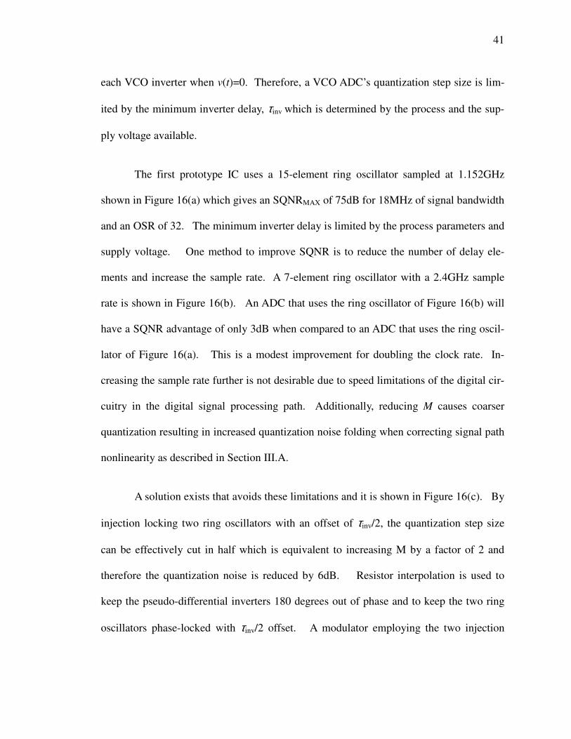
41
each VCO inverter when v(t)=0. Therefore, a VCO ADC’s quantization step size is lim-
ited by the minimum inverter delay, τinv which is determined by the process and the sup-
ply voltage available.
The first prototype IC uses a 15-element ring oscillator sampled at 1.152GHz
shown in Figure 16(a) which gives an SQNRMAX of 75dB for 18MHz of signal bandwidth
and an OSR of 32. The minimum inverter delay is limited by the process parameters and
supply voltage. One method to improve SQNR is to reduce the number of delay ele-
ments and increase the sample rate. A 7-element ring oscillator with a 2.4GHz sample
rate is shown in Figure 16(b). An ADC that uses the ring oscillator of Figure 16(b) will
have a SQNR advantage of only 3dB when compared to an ADC that uses the ring oscil-
lator of Figure 16(a). This is a modest improvement for doubling the clock rate. In-
creasing the sample rate further is not desirable due to speed limitations of the digital cir-
cuitry in the digital signal processing path. Additionally, reducing M causes coarser
quantization resulting in increased quantization noise folding when correcting signal path
nonlinearity as described in Section III.A.
A solution exists that avoids these limitations and it is shown in Figure 16(c). By
injection locking two ring oscillators with an offset of τinv/2, the quantization step size
can be effectively cut in half which is equivalent to increasing M by a factor of 2 and
therefore the quantization noise is reduced by 6dB. Resistor interpolation is used to
keep the pseudo-differential inverters 180 degrees out of phase and to keep the two ring
oscillators phase-locked with τinv/2 offset. A modulator employing the two injection

42
locked ring oscillators of Figure 16(c) with fS=2.4GHz has a 9dB increase in SQNR rela-
tive to a modulator using the oscillator of Figure 16(a) for the same signal bandwidth, BS.
Additionally, a delay cell using resistor feedback instead of weak inverter feedback is in-
herently faster and produces less thermal noise.
Alternately, a modulator employing two 7-element injection locked ring oscilla-
tors of Figure 16(c) with fS=2.4GHz can use the higher sampling rate to increase the sig-
nal bandwidth. For example, a modulator using a dual, 7-element injection-locked ring
oscillator with fS=2.4GHz and a 32x OSR will have a nearly identical SQNR but twice
the signal bandwidth when compared to a modulator using a single, 15-element ring os-
cillator with fS=1.152GHz.
The injection locking idea can be extended beyond two rings. For example, four
7-element rings can be injection-locked to further increase M by a factor of 2 and there-
fore reduce quantization noise by another 6dB. However, a dual, 7-element ring oscilla-
tor was chosen for the second prototype IC because it has 28 possible output codes values
which meet the SQNR target specification and allows reuse of the first prototype IC’s
digital processing blocks since its 5-bit signal processing path can process a 28 code ring
oscillator output.
VI.B. Quantization Noise Reduction by Extended No-
Overload Range
The output of the ∆Σ modulator, as described in Section II.A, is equal to the dif-
ference in VCO phase value from one sample to the next. This phase difference is lim-
43
ited to a range of 0-360 degrees. The measured phase difference value, as a function of
VCO frequency, sampled at the sample rate, fS, is periodic. In other words, multiple val-
ues of VCO frequency correspond to the same phase difference value. For example, if
the VCO frequency is equal to the sample frequency, then the sampled phase state does
not change from one phase sample to the next. But this is also true for
VCO S
f M f= ⋅ (27)
where M={0,1,2…} and the sample-to-sample measured phase difference is zero for all
values of M. If the sample-to-sample measured phase difference was plotted versus
VCO frequency, then the result would be a periodic triangle waveform with an amplitude
range of 0 to 360 degrees and a period of fS. The output of the ∆Σ modulator, which is
equal to this sample-to-sample measured phase difference, has a unique value only over a
frequency range of fS. Therefore, the VCO frequency range of operation must be limited
to
0.5VCO NOMINAL S
f f f= ± (28)
where fNOMINAL is the VCO frequency value when v(t)=0.
The ADC described in this paper is designed to operate with a nominal VCO fre-
quency equal to the sample rate, fS. which corresponds to differentiator output equal to
zero. Maximum and minimum differentiator output values occur at 0.5S S S
f f f= ±
therefore the no-overload range of operation corresponds to an instantaneous VCO fre-
quency of
44
( )0.5 1.5s VCO sf f t f< < . (29)
When the magnitude of the input voltage, v(t), causes fVCO(t) to be outside the value
specified in (29), then the VCO frequency of oscillation exceeds the full-scale range.
When the ring sampler samples the ring phase at the sample rate, fs, aliasing prevents the
ADC from determining correctly whether fvco(t) is above or below the range specified in
(29). An input signal that causes fvco(t) to exceed this range will result in an overloaded
and distorted output signal waveform. An example output waveform for the overloaded
ADC is shown in Figure 17(d). The output does not saturate like a flash converter in-
stead the output is severely distorted.
Fortunately, advantage can be taken of the large OSR of the converter. If the in-
put signal is changing slowly compared to fs, the previous oscillator sample value can be
used to determine the current sample value. This technique allows fvco(t) to extend be-
yond the range specified in (29).
A new block is added to the signal path called an Over-Range Corrector (ORC)
shown in Figure 17(a). Output data from the digital differentiator is fed into the ORC
block. A more detailed view of the ORC is shown in Figure 17(b). It consists of a
lookup-table based state-machine that compares the current output of the digital differ-
entiator, labeled a[n], with the past output of the ORC, labeled b[n-1]. A truth table is
shown in Figure 17(c) which describes the operation of the Overflow Logic block. A
simple algorithm is desirable to minimize die size and power dissipation in this block.
45
The Overflow Logic block uses simple logic to determine if the current value of a[n] is
within the range specified in (29) or above or below this range. If the current value of
a[n] is greater than 7 and the previous Overflow Logic output value, b[n-1], is less than
zero, then an over-range condition has occurred and 32 is subtracted from the current
value. In other words, the logic assumes that the current value must be negative because
the previous value was negative and an underflow situation has occurred. Conversely, if
the current value of a[n] is less than -8 and the previous Overflow Logic output value,
b[n-1] is greater than zero, then an over-range condition has occurred and 32 is added to
the current value of a[n]. In other words, the logic assumes that that current value must
be positive because the previous value was positive and therefore and overflow situation
has occurred. An example waveform at the output of the digital differentiator block is
shown in Figure 17(d) where the frequency of the ICRO, fVCO, swings above and below
the limits set by (29). Notice that aliasing causes the digital differentiator to decode
1.5VCO S
f f> as a value slightly greater than 0.5fS instead. The opposite occurs when
0.5VCO S
f f< and this condition is decoded as an fVCO value slightly less then 1.5fS. The
corrected output waveform at the output of the ORC block, without distortion, is shown
in Figure 17(e).
The ORC logic is only valid if the input signal is slow moving compared to the
sample rate. For the ORC to function properly, the input signal must not change more
than 8 digital differentiator output code values (out of a possible 32 values) per clock pe-
riod, TS, and therefore the input signal must be band-limited. If the digital differentiator
46
output code value changes by more than 8 code values per clock period, then an ambigu-
ous output is possible. For a sinusoidal input signal with a frequency of fS/2, its peak-to-
peak amplitude, AMAX-PP , must be less than 8
32PP
FS , where PP
FS is the peak-to-peak
full-scale input, to limit the differentiator output delta to less than 8 codes per sample pe-
riod, TS. For a sinusoidal input signal with a frequency of fS/4, the maximum peak-to-
peak amplitude must be less than ( )2 8PP
FS to guarantee that the differentiator output
does not travel more than 8 codes per sample period, TS. For all input signal frequencies
an input amplitude upper-bound limit can be established by limiting the slope of the input
signal to be less than 8
32PP
FS per sample period, TS. The slope of a sinusoidal input
signal is equal to 2IN PP
f FSπ , where fIN is the input sinusoid frequency. Since the input
signal voltage cannot travel more than 8
32PP
FS then it follows that the upper bound limit
for input amplitude is
4
S PPMAX PP
IN
f FSA
f π− = , (30)
where AMAX-PP is the maximum allowable peak-to-peak input signal for a given sample
rate, fS, and input sinusoid frequency, fIN. It follows from equation (30) that when fIN/fS
is less than 1/(4π), then no input signal band-limiting is required. The maximum at-
tenuation required is -15dBFS at fS/4 and -12dBFS at fS/2. A single-pole filter at fS/4π
provides sufficient filtering to meet the requirements of (30) because the roll-off of a sin-

47
gle pole filter is equal to the change in sinewave slope versus input frequency, fIN For
example, with a 2.4GHz sample rate, fS, a single pole at 190MHz is sufficient to band-
limit the input signal.
The ORC function improves the performance of the ∆Σ modulator in two ways.
First, it can be used to extend the dynamic range of the converter. In theory, the over-
range corrector can extend the VCO frequency range well beyond that shown in (29).
However, for this test chip, the over-range corrector was limited to extending the differ-
entiator output range from 28 to 32 possible levels which corresponds to a 1dB increase
in dynamic range. The ADC was not allowed to extend beyond that range for two rea-
sons. First, exhaustive simulation and silicon data shows that the nonlinearity of the
VCO in the 0.5fS to 1.5fS range tends to be well modeled as a weakly nonlinear function
that can in turn be modeled as a Taylor series as mentioned previously in Section III.A.
If the VCO is to be used beyond the 0.5fS to 1.5fS range, then care must be taken to ensure
that the VCO continues to exhibit a weakly nonlinear function. At some point as the
VCO is driven farther beyond the range specified in (29), the current-to-frequency trans-
fer function will transitions from a “weak” to a “hard” nonlinearity where higher order
terms become significant. Extending the usable range further would have increased the
achievable overall SNR but at the expense of reduced SNDR with a full scale input. Sec-
ond, re-use of the original 5-bit signal process path was desirable. The 5-bit signal proc-
essing allows for 32 possible output codes where a maximum positive output code is +15
and a maximum negative output code is -16.
48
Additionally, the ORC allows for more usable dynamic range in the converter be-
cause, practically speaking, the maximum input signal can be allowed to exist closer to
full-scale since an input signal excursion slightly beyond full-scale results in a much
smaller error with the over-range corrector enabled.
Second, the ORC function improves the overload performance of the VCO-based
∆Σ modulator. A traditional ∆Σ ADCs behave poorly when the input exceeds full scale
resulting in modulator instability poor recovery time and unusable output codes. This
new design behaves very differently – it saturates like a flash converter. This behavior is
important for many applications. When the input signal exceeds full scale the output of
the over-range corrector saturates at codes +15 or -16 as shown in Figure 17(f). This fea-
ture also allows for over-range detection.
VI.C. Dither
As discussed in Section III.C, the quantization noise from a first-order ∆Σ modu-
lator is very poorly behaved and for low-amplitude input signals the output may contain
large spurious tones. The self-cancelling dither technique presented in Section III.C is
used to eliminate the spurious tone problem by adding dither sequences prior to quantiza-
tion and then cancelling them in the digital domain.
VI.C.1 Case #1: Extremely Linear V/I Converter
From a practical circuit point of view, it is extremely difficult to add a dither sig-
nal as a voltage prior to the V/I converter. However, it is trivial to add dither as a current

49
with a simple current steering DAC at the output of the V/I converter. One method to
create self-cancelling dither is shown in Figure 18(a). Dither is added as a common-
mode signal to the signal path through two 4-level DACs. The digitized outputs of the
two converters are subtracted resulting in a doubling of the signal level and a cancelling
of the dither signal.
Problems arise with this self-cancelling dither scheme when nonlinearity exists in
the signal path. The first prototype IC corrects for the 2nd
and 3rd
order distortion of the
ICRO. However, as mentioned in Section III.B, the 2nd
order distortion is large and can-
celling it perfectly is difficult due to channel-to-channel mismatch as well as bandwidth
limitations in the system. Recall that the pseudo-differential architecture was used to
remove the resulting residual uncorrected even-order distortion. Assuming the distortion
can be modeled with a small number of Taylor series coefficients, the nonlinearity distor-
tion coefficients for the ICRO are α2 and α3. The output of each channel’s differentiator
is
2 2
2 3[ ] [ ] ( [ ]) ( [ ]) [ ]CH CH CH CH
y n n n n e nω α ω α ω ∆Σ= + + + , (31)
where CH is the channel number, either 1 or 2 for this first example, and the channel’s
input signal is
1
2
[ ] [ ] [ ]
[ ] [ ] [ ]
I
I
n n d n
n n d n
ω ωω ω
= + += − +
, (32)
where d[n] is the discrete-time dither signal integrated over one sample interval and ωΙ[n]
50
is the input signal, vI(t), integrated over one sample interval and multiplied by KVCO. The
nonlinearity coefficient estimator calculates the correction terms 2αɶ and 3αɶ . Consider the
case mention above, where the third order estimated term is exactly equal to the actual
distortion coefficient ( 3 3α α=ɶ ) but the second-order estimate is not perfect ( 2 2α α≠ɶ ).
Substituting (32) into (31), then (31) into (18) gives the corrected output of channel 1 and
channel 2 of Figure 18(a). Taking the difference of the channel 1 and channel 2 corrected
outputs gives the following
1 2 2 2[ ] [ ] 2 [ ] 4( ) [ ] [ ] ...
0
OUT corrected corrected I Iy y n y n n n d nω α α ω= − = + − +
≠
ɶ�����
(33)
The un-cancelled second-order distortion causes common-mode dither signal to be con-
verted to differential signal through the residual uncorrected 2nd
order distortion shown in
the second term of (33). Because the second order distortion is very large, the residual,
uncorrected 2nd
order distortion can be quite large and therefore the conversion of com-
mon-mode dither signal to differential-signal can be quite large.
For this reason, the dual pseudo-differential architecture with differential dither
DACs shown in Figure 18(b) was chosen for the first prototype IC because it eliminates
the common-mode to differential conversion seen in (34). The input signal is injected
differentially into the two pseudo-differenital channels with the same polarity but the
dither signal is injected differentially into the two pseudo-differential channels with the
opposite polarity. Therefore, the input signals for the four channels are
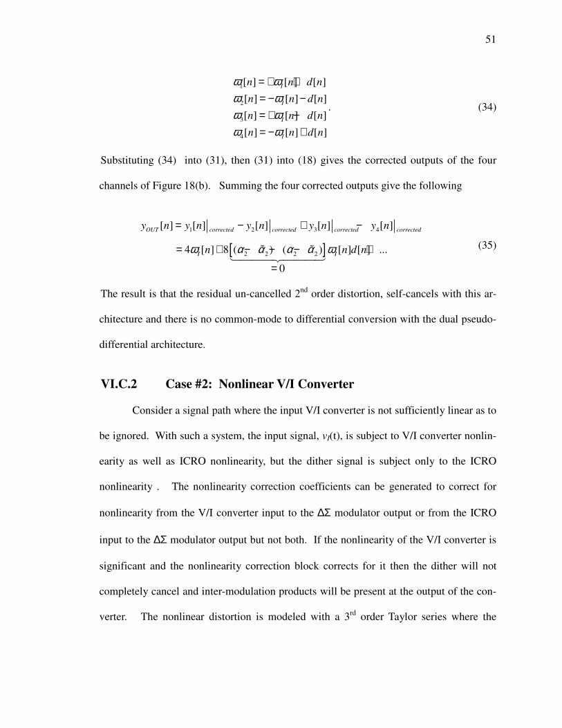
51
1
2
3
4
[ ] [ ] [ ]
[ ] [ ] [ ]
[ ] [ ] [ ]
[ ] [ ] [ ]
I
I
I
I
n n d n
n n d n
n n d n
n n d n
ω ωω ωω ωω ω
= + += − −= + −= − +
. (34)
Substituting (34) into (31), then (31) into (18) gives the corrected outputs of the four
channels of Figure 18(b). Summing the four corrected outputs give the following
[ ]1 2 3 4
2 2 2 2
[ ] [ ] [ ] [ ] [ ]
4 [ ] 8 ( ) ( ) [ ] [ ] ...
0
OUT corrected corrected corrected corrected
I I
y n y n y n y n y n
n n d nω α α α α ω
= − + −
= + − − − +
=
ɶ ɶ���������
(35)
The result is that the residual un-cancelled 2nd
order distortion, self-cancels with this ar-
chitecture and there is no common-mode to differential conversion with the dual pseudo-
differential architecture.
VI.C.2 Case #2: Nonlinear V/I Converter
Consider a signal path where the input V/I converter is not sufficiently linear as to
be ignored. With such a system, the input signal, vI(t), is subject to V/I converter nonlin-
earity as well as ICRO nonlinearity, but the dither signal is subject only to the ICRO
nonlinearity . The nonlinearity correction coefficients can be generated to correct for
nonlinearity from the V/I converter input to the ∆Σ modulator output or from the ICRO
input to the ∆Σ modulator output but not both. If the nonlinearity of the V/I converter is
significant and the nonlinearity correction block corrects for it then the dither will not
completely cancel and inter-modulation products will be present at the output of the con-
verter. The nonlinear distortion is modeled with a 3rd
order Taylor series where the
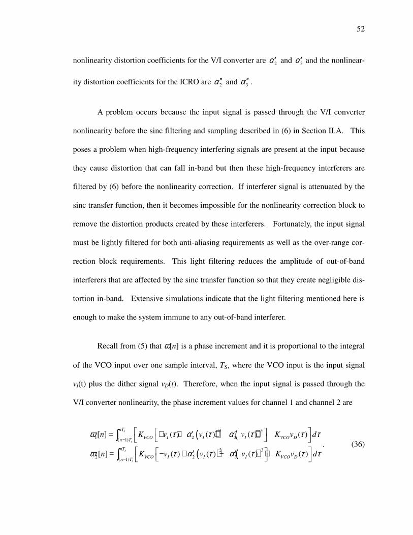
52
nonlinearity distortion coefficients for the V/I converter are 2α ′ and 3α ′ and the nonlinear-
ity distortion coefficients for the ICRO are 2α ′′ and 3α ′′ .
A problem occurs because the input signal is passed through the V/I converter
nonlinearity before the sinc filtering and sampling described in (6) in Section II.A. This
poses a problem when high-frequency interfering signals are present at the input because
they cause distortion that can fall in-band but then these high-frequency interferers are
filtered by (6) before the nonlinearity correction. If interferer signal is attenuated by the
sinc transfer function, then it becomes impossible for the nonlinearity correction block to
remove the distortion products created by these interferers. Fortunately, the input signal
must be lightly filtered for both anti-aliasing requirements as well as the over-range cor-
rection block requirements. This light filtering reduces the amplitude of out-of-band
interferers that are affected by the sinc transfer function so that they create negligible dis-
tortion in-band. Extensive simulations indicate that the light filtering mentioned here is
enough to make the system immune to any out-of-band interferer.
Recall from (5) that ω[n] is a phase increment and it is proportional to the integral
of the VCO input over one sample interval, TS, where the VCO input is the input signal
vI(t) plus the dither signal vD(t). Therefore, when the input signal is passed through the
V/I converter nonlinearity, the phase increment values for channel 1 and channel 2 are
( ) ( )
( ) ( )
2 3
1 2 3( 1)
2 3
2 2 3( 1)
[ ] ( ) ( ) ( ) ( )
[ ] ( ) ( ) ( ) ( )
s
s
s
s
nT
VCO I I I VCO Dn T
nT
VCO I I I VCO Dn T
n K v v v K v d
n K v v v K v d
ω τ α τ α τ τ τ
ω τ α τ α τ τ τ
−
−
′ ′= + + + +
′ ′= − + − +
∫
∫. (36)
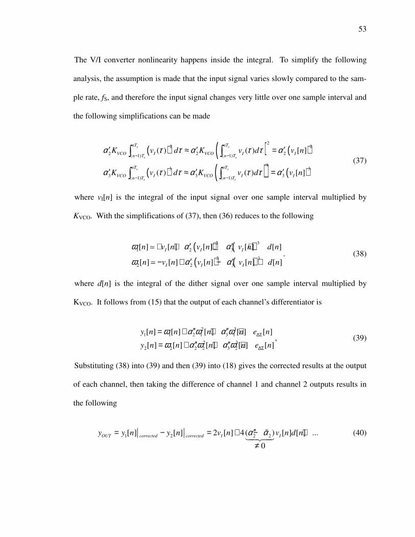
53
The V/I converter nonlinearity happens inside the integral. To simplify the following
analysis, the assumption is made that the input signal varies slowly compared to the sam-
ple rate, fS, and therefore the input signal changes very little over one sample interval and
the following simplifications can be made
( ) ( ) ( )
( ) ( ) ( )
22 2
2 2 2( 1) ( 1)
33 3
3 3 3( 1) ( 1)
( ) ( ) [ ]
( ) ( ) [ ]
s s
s s
s s
s s
nT nT
VCO I VCO I In T n T
nT nT
VCO I VCO I In T n T
K v d K v d v n
K v d K v d v n
α τ τ α τ τ α
α τ τ α τ τ α
− −
− −
′ ′ ′≈ =
′ ′ ′≈ =
∫ ∫
∫ ∫ (37)
where vI[n] is the integral of the input signal over one sample interval multiplied by
KVCO. With the simplifications of (37), then (36) reduces to the following
( ) ( )( ) ( )
2 3
1 2 3
2 3
2 2 3
[ ] [ ] [ ] [ ] [ ]
[ ] [ ] [ ] [ ] [ ]
I I I
I I I
n v n v n v n d n
n v n v n v n d n
ω α α
ω α α
′ ′+ + + +
′ ′− + − +
≃
≃. (38)
where d[n] is the integral of the dither signal over one sample interval multiplied by
KVCO. It follows from (15) that the output of each channel’s differentiator is
2 3
1 1 2 1 3 1
2 3
2 2 2 2 3 2
[ ] [ ] [ ] [ ] [ ]
[ ] [ ] [ ] [ ] [ ]
y n n n n e n
y n n n n e n
ω α ω α ωω α ω α ω
∆Σ
∆Σ
′′ ′′= + + +′′ ′′= + + +
, (39)
Substituting (38) into (39) and then (39) into (18) gives the corrected results at the output
of each channel, then taking the difference of channel 1 and channel 2 outputs results in
the following
1 2 2 2[ ] [ ] 2 [ ] 4( ) [ ] [ ] ...
0
OUT corrected corrected I Iy y n y n v n v n d nα α′′= − = + − +
≠
ɶ�����
(40)
54
Perfect estimation of the combined V/I converter and ICRO nonlinearity results in sec-
ond and third order correction terms equal to 2 2 2α α α′ ′′= +ɶ and 3 3 3α α α′ ′′= +ɶ , respectively.
If the V/I converter distortion is large then the term 2 2( )α α′′ − ɶ is very large and therefore
the dither and input signal inter-modulation at the output of the ADC shown as the second
term in (40) is very large. Given a full-scale input signal, a typical dither signal that is
roughly equal to 1dB of the input full scale range, and V/I converter and ICRO distortion
components of similar magnitude as described in II.C, extensive simulations show that
the un-cancelled dither signal present at the output will be significant and severely reduce
the performance of the ADC.
However, a solution exists that greatly reduces the severity of this problem: the
dual pseudo-differential converter shown in Figure 18(b) described in the previous sec-
tion. Recall that the input signal, v(t), is added differentially to each pseudo-differential
converter channel and the dither signal is added as a differential signal to each pseudo-
differential signal path but with the opposite polarity. The outputs of the two pseudo-
differential channels are added with the result that the digitized input signal adds at the
output but the digitized dither signal largely cancels at the output. As in the case of the
single pseudo-differential converter in Figure 18(a), the dual pseudo-differential con-
verter gives undesired inter-modulation terms at the output. However, in the dual
pseudo-differential architecture all the even-order undesired terms cancel leaving only the
odd-order terms

55
[ ]1 2 3 4
2 2 2 2
2 2
2 2 2 3 3
[ ] [ ] [ ] [ ] [ ]
4 [ ] 8 ( ) ( ) [ ] [ ]
0
12 2( ) ( ) [ ] [ ] ...
0
OUT corrected corrected corrected corrected
I I
I
y n y n y n y n y n
n n d n
n d n
ω α α α α ω
α α α α α ω
= − + −
′′ ′′= + − − −
=
′′ ′′ + − + − +
≠
ɶ ɶ���������
ɶ ɶ ɶ�����������
(41)
Fortunately, the second term in (41) completely cancels and the third term in (41) is very
small because the dither signal and the second-order distortion terms are both squared
and the third-order term is small. Given a full-scale input signal, a 1dBFS dither signal
and V/I converter and ICRO distortion components of similar magnitude as described in
II.C, extensive simulations show that the inter-modulation product falls well below the
noise floor and has no effect on the overall SNR.
It can be shown that a converter with 4 psuedo-differential channels can be con-
figured so that the third-order terms also cancel at the output of the converter. However,
this approach was not taken because the added complexity outweighs any potential bene-
fit for this application.
These results make possible the use of a moderately nonlinear V/I converter. This
approach will be investigated in the next section.
VI.D. Low Voltage V/I Converter
The closed-loop V/I converter used in the first prototype IC required a 2.5V sup-
ply and a feedback amplifier to create a highly linear voltage-to-current conversion as
shown in Figure 19(a). This ADC front-end is perfectly suited for applications requiring
56
a low-bandwidth, moderately high dynamic range AFE signal path that uses a 2.5V sup-
ply. However, the first prototype IC’s V/I converter would not interface well in applica-
tions using a 1.2V signal path.
Fortunately, the dual pseudo-differential architecture described in the previous
section allows for the use of a moderately nonlinear V/I converter. A much simpler V/I
converter can be constructed which uses a 1.2V supply and consumes much less power
and produces less noise. The V/I converter chosen is a simple, open-loop, resistor-
degenerated pMOS common-source amplifier shown in Figure 19(b). The V/I converter
operates from a 1.2V supply, so it uses thin-oxide transistors. The V/I converter input
common-mode is chosen to be roughly mid-supply. Headroom limitations at the output
of the V/I converter limit the amount of resistor degeneration resulting in a fairly small
amount of linearization improvement in the voltage-to-current conversion relative to a
non-degenerated common-source amplifier.
Headroom allowed for a degeneration resistance that corresponded to roughly a
200mV drop across this resistor with a zero differential input signal. The degeneration
resistance is typically 310 ohms which is roughly 3 times greater than the transistor tran-
simpedance, gM -1
. The full-scale input swing for fS=2.5GHz is 800mV differential peak-
to-peak with a KVTI approximately equal to 2.2mS. Simulations indicate that for each ∆Σ
modulator, the input referred noise voltage for the V/I converter degeneration resistors
and V/I converter pMOS devices are 5.4nV Hz and 2.9 nV Hz , respectively. Simu-
lations indicate that the V/I converter 1/f noise corner occurs at roughly 400 kHz. This
57
noise corner is fairly high due to the small area of the V/I converter pMOS devices and
the limited degeneration resistance used. If a lower 1/f noise corner is required, then ei-
ther higher degeneration or larger pMOS devices are required – the penalty for this is
greater headroom requirements for the V/I converter or greater parasitic capacitance at
the current starved node of the ICRO which will increase AC distortion in the signal path
(more about this in section VII.C). The low-pass ring oscillator phase noise is subjected
to the high-pass transfer function of the 1-z-1
blocks, so the resulting contribution to the
output sequence in the signal band is nearly white noise. Simulations indicate that the
ICRO noise is very small relative to the V/I converter noise referred to the input of the
converter.
The open-loop V/I converter’s transfer function is close to that of a resistor de-
generated square law device with a fairly strong second-order distortion term but a fairly
small third-order distortion term. It is interesting to note that the second, third, and
fourth order distortion terms of the open-loop V/I converter have similar amplitudes but
opposite signs to that of the ICRO. These distortion terms tend to negate each other
which results in lower overall distortion through the system. For example, the output of
the simulated open-loop V/I converter with a near full-scale 250KHz sinusoidal input
signal has second, third, and fourth harmonics at -29 dBc, -43 dBc, -60dBc, respectively.
These numbers closely match the distortion term reported for the ICRO of section II.B
which has second, third, and fourth harmonics at -26dBc, -47dBc, and -64dBc, respec-
tively The overall converter distortion including the open-loop V/I converter and the
ICRO with a 250KHz sinusoid input signal had second, third, and fourth harmonics at -

58
35dBc, -49dBc, and -66dBc, respectively.
Recall from Section VI.D that V/I converter third order distortion can cause un-
cancelled dither signal to fall into the signal band. Exhaustive simulations indicate that
for a V/I converter with a third harmonic term of -43dBc and a dither signal amplitude of
-26dBFS (which corresponds to a peak-to-peak dither signal roughly equal to the quanti-
zation step size) the resulting un-cancelled dither inter-modulation products are below the
noise floor.
Care must be exercised to ensure that the V/I converter’s nonlinearity can be well
modeled as a weakly nonlinear function that, in turn, can be modeled as a Taylor series as
mentioned previously in section III.A. This requirement is ultimately what sets the re-
quired degeneration resistor value. The minimum power supply voltage minus the
maximum output swing of the ICRO sets the minimum headroom for the V/I converter.
It is necessary to keep the degenerated pMOS device well in saturation at all times in or-
der to keep the V/I converter transfer function equivalent to a weak nonlinearity. Unfor-
tunately, the small headroom budget limited the amount of resistor degeneration. Due to
this limited resistor degeneration, the V/I converter nonlinearity transitions from a weak
to a strong nonlinearity at roughly -2.5dBFS. For input signals with amplitudes greater
than -3dBFS, the weak linearity model begins to break down and the nonlinearity correc-
tion block fails to adequately correct the nonlinearity which results in a reduction in
SNDR for input signals greater than -3dBFS. (This is another reason why the overload
range extension mentioned in Section VI.B was not pushed much beyond the nominal
59
range.)
Two open-loop V/I converters are configured in a pseudo-differential fashion as
shown in Figure 19(b) but unfortunately this configuration provides no input-signal com-
mon-mode rejection. In other words, the input common-mode dc bias point sets the dc
bias current flowing into the ICRO which therefore sets the center frequency of the
ICRO. A calibration unit is required to set the correct ADC input common-mode voltage
which will align the ICRO center frequency with the ADC sample rate, fs.
VI.E. Digital Background Calibration
As mentioned in Section III.A, two types of digital background calibration are re-
quired for each ADC. The first is digital background calibration of the V/I converter and
ICRO induced second-order and third-order distortion which addresses the signal path
nonlinearity problem described previously. The second is digital background tuning of
the VCO’s center frequency to match the ADC’s sample rate, fS, which centers the input
range of the ADC about the midscale input voltage and therefore maximizes dynamic
range as well as enables reconfigurability by automatically retuning the VCO’s center
frequency whenever fS is changed.
Using a nonlinear V/I converter increases the implementation difficulty of the
calibration unit substantially. In the first prototype IC’s calibration unit, the V/I con-
verter is assumed to be sufficiently linear and only the ICRO nonlinearity is estimated.
Since the ICRO has a current input, it is a simple matter to inject the calibration sequence

60
as a current via a simple current steering DAC. However, a signal path employing a
nonlinear V/I converter requires that the calibration signal be injected as a voltage at the
V/I converter input so that both the nonlinearity of the V/I converter and the ICRO can be
estimated. This requires the use of a voltage DAC which is significantly more difficult
to implement than a current DAC. Figure 20 shows a detailed description of the new
calibration unit including the voltage mode calibration DAC. The operation of this new
calibration unit will be described in the following three sub-sections.
VI.E.1 Nonlinearity Correction
Recall that the nonlinearity correction block in the signal path is a high speed
look-up table with mapping data updated periodically by the nonlinearity coefficient cal-
culator block of the calibration unit. The look-up table maps each 5-bit input sample,
y[n], into an output sample, y[n]|corrected, such that
( ) ( )( )32 22
1 2 3 2 2corrected[ ] [ ] [ ] ( 2 ) [ ] [ ]y n G y n y n y n y nα α α α = − − − −
ɶ ɶ ɶ ɶ (42)
where 2αɶ and 3αɶ are estimates of the α2 and α3 signal path distortion coefficients and G1
is a gain scaling factor.
VI.E.2 Nonlinearity Coefficient Measurement
The Nonlinearity Correction Block needs to first measure the nonlinearity intro-
duced by the V/I converter and ICRO in the signal converter shown at the top of Figure
20. This is accomplished by measuring the nonlinearity of a signal converter replica. A
voltage-mode DAC consisting of a current-steering DAC and load resistors are used to
61
generate a calibration sequence at the input to the signal converter replica. Since the ref-
erence current is proportional to a precision reference divided by the on-chip poly resistor
value, it follows that output of the voltage DAC is proportion to the reference voltage
which results in a very precisely controlled amplitude. The amplitude of the calibration
DAC is proportional to an 8-bit programmable value, dDAC[7:0]. The calibration se-
quence is therefore passed through the V/I converter and the ICRO. Signal path nonlin-
earity produces intermodulation products that can be correlated against to estimate the
nonlinear coefficients of the signal path replica.
The level of the calibration signal is important - it should be between 0.4FS and
1.0FS. It must be greater than 0.4FS because the calibration signal itself is used to dither
the replica converter signal path. Exhaustive simulation and silicon measurements show
that this minimum level of signal is required to get a good estimate of the 3rd
order coeffi-
cient. When the calibration signal falls below this level then spurious content can cor-
rupt the coefficient estimates. It is easy to verify the amplitude of the calibration se-
quence by viewing the output of the correlators. The calibration unit continuously
measures the gain of the signal path replica by correlating its output against one of the
three 2-level sequences, t1[n], to obtain the fs/228
-rate sequence given by
[ ] [ ] [ ]1
1 1
0
1 P
i
m r mP i t mP iP
γ−
== + +∑ (43)
where P = 228
. Since the calibration output has 4 levels and there are 32 possible output
codes, a full-scale calibration sequence should have a step size of 31
3 output codes. It
62
follows that a single calibration sequence at the output of the replica signal path has a
full-scale peak amplitude of 1 31
2 3⋅ and when this output is multiplied by its correspond-
ing +/-1 calibration sequence and summed over P=228
clock cycles, then the following
sum is expected at the first correlator output
28 9
1
1 312 1.39 10
2 3FULL SCALE
γ − − = ⋅ = × . (44)
The calibration state machine can servo the amplitude of the calibration sequence until
the γ1 value is the desired percentage of full-scale. This can be accomplished in one step
after the first value of γ1 is measured by changing the amplitude of the calibration DAC
with the following equation
9
1
1.39 10[7 : 0] [7 : 0]
DAC DESIRED DAC INITIAL CAL
INITIAL
d d Kγ− −
−
×= ⋅ ⋅ (45)
where dDAC-INITIAL[7:0] is the initial value of the calibration DAC, γ1-INITIAL is the initial
measured value of γ1, and KCAL is a constant representing the target percentage of full
scale for the calibration sequence, a value between 0.4 and 1.0.
The value of γ1 also provides the user with a precise measurement of the gain of
the signal converter. There are two ways to reference the output full-scale of the con-
verter. First, the full-scale output of the converter can be referenced to the output code
of the digital differentiator by setting G1=K1, where K1 is a constant that allows use of the
full 16-bit output range of the converter. A typical value of K1 is 1024 which roughly cor-
63
responds to +/-16384 for a full-scale input signal. Second, the full-scale output of the
converter can be referenced to a known voltage by setting G1=K2 dDAC[7:0] / γ1[m] where
K2 is a constant that allow for full use of the 16-bit output range of the converter and
dDAC[7:0] is the 8-bit digital amplitude value of the calibration DAC. A typical value for
K2 is 3.2x10⁹ which gives an output code of +/-16384 for an input of +/-200mV for all
process corners and temperatures.
The calibration unit continuously measures α2 and α3 as described in Section III.A.3 and
the estimates 2αɶ and 2αɶ are given in (23). As before, it does this and loads the 32 values
into the nonlinearity correction block’s look-up table at a maximum rate of once every
228
TS seconds.
VI.E.3 VCO Center Frequency Calibration
To maximize dynamic range of the signal converter, the center frequency of the
ICRO is tuned to the sampling frequency, fS. The calibration sequence injected into the
replica signal converter is zero-mean. Therefore it is a simple matter to calculate the off-
set of the signal converter in terms of LSBs from the ICRO
[ ] [ ]1
0
0
1 P
i
m r mP iP
γ−
== +∑ . (46)
A feedback loop is implemented to drive γ0 to be zero as described in section III.A.
When γ0 is zero the replica ICRO center frequency is very close to the sample frequency,
fS.
64
This concept is very simple and the implementation is quite simple for the calibra-
tion unit of the first prototype IC. However, the implementation is much more difficult
when the calibration sequence drives the open-loop V/I converter. A problem arises in
that the V/I converter has no inherent common-mode rejection. In fact the V/I converter
input common-mode voltage sets the V/I converter DC bias current.
The calibration source shown in Figure 21(c) consists of two parts. First, the cali-
bration DAC, IDAC, sets the calibration signal voltage swing at the replica V/I converter
input. Second, the calibration DAC, IDAC, plus the common-mode current sources, ICM,
set the DC bias point for the replica V/I converter. The calibration DAC load network,
RCAL plus MCAL, was intentionally designed to mimic stack-up of the V/I converter. The
sizes of MDAC and RDAC are chosen so that they mimic the V/I converter transistor, MVTI,
and degeneration resistor, RVTI, with the result that the two circuits act like a crude cur-
rent mirror. In this way, the nominal current in the V/I converter is roughly equal to
3
[7 : 0]2
VTI DAC CM CAL CENTERI I I K d≈ + = (47)
where IDAC is the tail current in each of the 3 DAC elements, ICM is the current in the
common-mode current sources, KCAL is a constant and dCENTER[7:0] is the 8-bit control
value from the VCO center frequency calculator block. This circuit has the desirable
property that the initial guess at the center current is fairly accurate since the ICRO fre-
quency versus input current can be estimate quite accurately and does not vary signifi-
cantly over process, temperature, and supply voltage.

65
The single-ended peak-to-peak output swing of the calibration DAC is
( )3DAC DAC CM
I R R where RCM>>RDAC and IDAC is equal to KCAL dDAC[7:0].
Additionally, some simple logic was added at the bottom of Figure 21 to ensure
that the value of dDAC[7:0] is never larger than the centering control word, dCENTER[7:0].
The ADC signal path must be configured to have the same bias point as the rep-
lica V/I converter input. This is accomplished with the two common-mode sensing resis-
tors, RCM, that create a voltage, VCM, which is equal to the calibration signal common-
mode voltage – in other words, its nominal voltage. This voltage, VCM, is used to set the
input common-mode of the signal converter. It does so by controlling the common-
mode output of the circuit driving the signal converter. For example, in Figure 21(a),
the ADC is driven by an off chip transformer where VCM sets the center tap voltage of the
transformer. Alternately, in Figure 21(b), the ADC is driven by an active circuit with the
output common-mode set by the VCM voltage. Care must be taken to minimize the driv-
ing circuit common-mode error – any deviation from the value supplied by the calibration
unit, VCM, will result in lost dynamic range in the signal converter.
66
VII. CIRCUIT LEVEL ENHANCEMENTS
VII.A. Achieving Theoretical Maximum SQNR
The SQNR measured in the first prototype IC in section V was roughly 2-3dB be-
low the theoretical maximum achievable. Three primary factors were involved in this
reduction of achieved SQNR.
Firstly, random device mismatch in each delay cell transistor and also in the ring
sampling flip-flops leads to a mismatch in the unit delay size. This is equivalent to quan-
tizer INL error which leads to distortion and therefore an increase in quantization noise.
Not much can be done here except to ensure fast rise and fall times for phase output sig-
nal.
Secondly, offsets in the closed-loop V/I converters led to small mismatches in the
ICRO center frequency current generated by the V/I converter. This led to a slight mis-
match in center frequency value for each of the four rings oscillators. This is equivalent
to an input referred voltage offset at the input of each of the four ICROs which slightly
reduces the maximum swing available to all the ICROs. In the first prototype IC, the
two V/I converters in each ADC had all bias voltages common except for VBIAS3 and
VBIAS4 as shown in Figure 19(a). Separate bias networks were used to generate the VBIAS3
and VBIAS4 voltages and device mismatch caused random error in the center frequency
current value that was as large as +/-1LSB, which resulted in a maximum reduction of
67
usable headroom of around 0.5dB. This error can be reduced significantly by making
common all of the DC bias voltages between the two V/I converters.
Lastly, and most importantly, non-uniform layout of each delay element led to un-
equal unit delay size among all the ICRO delay elements. This led to distortion and re-
duced quantization noise performance of approximately 1dB. Care was taken in the new
layout to keep the layout of each delay cell very uniform and also to keep the cell-to-cell
routing very uniform in order that the unit delay is kept very uniform.
VII.B. Signal Path AC Nonlinearity
The frequency dependent nonlinearity in the first prototype IC limited its per-
formance for larger input frequencies and bandwidths. This frequency dependent distor-
tion can be seen in Figure 13(b). Excessive parasitic capacitance at the current starved
node of the ring oscillator was the primary cause of this roll-off in performance at higher
input frequencies. Capacitance at the current starved node of the ring oscillator results in
frequency dependent phase shift between input signal and the distortion components
which lie at different frequencies. The nonlinearity correction block only corrects for DC
nonlinearity. Nonlinear phase shift at the current starved node of the ring oscillator
keeps the DC nonlinearity correction from being effective. As the frequency increases
the phase shift increases and the DC correction become less and less effective resulting in
less and less effective distortion correction. Two approaches were taken to reduce the
parasitic capacitance.

68
Firstly, parasitic metallization capacitance on each of the ICRO current starved
nodes must be minimized. Each of the four current starved nodes must be routed to the
dither DAC. Care must be taken to minimize the parasitic routing capacitance on this
node. The first prototype IC used poor layout resulting in excessive routing capacitance
on all four current starved nodes. This routing capacitance was primarily responsible for
the AC distortion.
Secondly, diffusion capacitance at the ICRO current starved node must be mini-
mized. The current starved node connects to the source node of each and every delay
cell pMOS device. In the first prototype IC, the delay cell pMOS devices, labeled MP1
and MP2 in Figure 16(b), were each constructed of two parallel devices which shared a
diffusion node at their drains. Doing so minimized capacitance on the output node of the
delay cell resulting in a slightly faster delay element. Unfortunately doing so caused the
pMOS transistor to have twice as much diffusion area on its source which is connected to
the current starved node of the ring oscillator. For the second prototype IC, the pMOS
diffusion sharing was swapped. In this new configuration, the delay cell output node has
the non-shared diffusion node and thus more diffusion capacitance resulting in a slightly
slower delay cell but a slightly faster ICRO current starved node due to the reduction in
diffusion capacitance on the pMOS source node and therefore less capacitance on the
ICRO current staved node.
These two improvements significantly increased AC linearity as will be shown in
the following measurement results section.
69
VII.C. Ring Sampler Hysteresis Problem
The first prototype IC exhibits some high, odd-order distortion terms that can be
seen in the output spectrum of Figure 12. For a full-scale, low frequency input signal,
with the nonlinearity correction enabled, distortion terms greater than 3rd
order are ex-
pected to be insignificantly small. However, distortion terms at frequencies equal to 5, 7,
9, and 11 times the fundamental frequency are present in the output spectrum at levels
slightly below the 80dBFS. The value of distortion is fairly small but it is desirable un-
derstand the cause of this distortion and find a simple fix that removes these distortion
components.
The first prototype IC’s ring sampler uses a transmission-gate based D-type flip-
flop to sample the outputs of the ICRO. This flip-flop is shown in Figure 22(a). The
previous ICRO phase sample is stored on the internal node of the flip-flop at the node la-
beled c. When the flip-flop transitions from hold to sample mode, the transmission gate
across nodes b and c becomes low impedance and the inverter driving node b must charge
or discharge the capacitance on both nodes b and c. This can result in a data-dependent
sampling error which leads to distortion and to the high-order harmonic distortion com-
ponents seen in Figure 12. This problem is easily solved by using a non-transmission-
gate based flip-flop in the ring sampler as shown in Figure 22(b). With this new flip-
flop, the sampling decision is not effected by the previous sample. The resulting im-
proved distortion performance will be demonstrated in the following measurement results
70
section.
VII.D. Process Scaling
The 65nm G+ process is superior to the 65nm LP process for the VCO-based
ADC because the transistors are faster and lower power. The 65nm G+ process transis-
tors have lower threshold voltages and smaller effective gate lengths than their counter-
parts in the LP process. This combination allows digital logic to run much faster with the
same supply voltage in the G+ process compared to the LP process. This extra speed al-
lows the VCO ADC to operate at a faster sample rate, fS, which can be used to increase
signal bandwidth or increase the OSR and therefore reduce quantization noise. The G+
logic gates can dissipate less power than LP logic gates by running the G+ logic off a
lower power supply voltage. For example, simulations indicate that logic cells in the G+
process with a power supply of 0.9V are faster than identical logic cells in the LP process
with a 1.2V power supply. Digital logic power dissipation is proportional to CPVDD2
where CP is the parasitic capacitance driven by the logic circuitry and VDD is the supply
voltage. Since power dissipation is roughly proportional to the square of the power
supply voltage, digital circuit power dissipation drops quickly with a reduction in power
supply voltage. Simulations indicate that the power dissipation of identical digital logic
blocks is 40% less in the G+ process compared to the LP process when the G+ logic op-
erates with a 0.9V supply and the LP logic operates with a 1.2V supply. Because the
VCO ADC performance is extremely reliant on digital gate speed and power, the G+
process gives this architecture a large boost in performance. The advantages of the 65nm

71
G+ process versus the 65nm LP process will be apparent in the following two sections
that show measurement results for two prototype ICs manufactured in the 65nm G+ proc-
ess.
72
VIII. SECOND PROTOTYPE IC
VIII.A. Measurement Results
The second prototype IC was fabricated in the TSMC 65nm G+ process with the
deep nWell option and both single-oxide and dual-oxide devices, but without the MiM
capacitor option. All pads have ESD protection circuitry. The IC was packaged in a 64-
pin LFCSP package.
The second prototype IC contains two ∆Σ modulators that incorporate all of the
architectural and circuit enhancements described in Sections VI and VII. The combined
area of the two ∆Σ modulators, the calibration unit, and the ADC bias circuitry totaled
0.15mm2. A die photograph of one of the ∆Σ modulators is shown in Figure 23. The
calibration unit area is 0.07mm2. The signal converter, i.e., the portion of each ∆Σ modu-
lator not including the calibration unit, has an area of 0.04mm2. A single calibration unit
is shared by the two ∆Σ modulators, so the area per ∆Σ modulator is 0.075mm2. All
components of both ∆Σ modulators and the calibration unit are implemented on-chip in-
cluding the fS/228
-rate coefficient calculation block. The calibration unit area on the sec-
ond prototype is 0.01mm2 larger than the first prototype IC due to the addition of the
fS/228
-rate coefficient calculation block on the silicon. Additionally, a digital decimator
was included on chip to reduce the output data rate by a factor of 8. As is typical for ∆Σ
modulator ADC figure-of-merit calculations, decimator die size was not included in the

73
∆Σ modulator area calculation and the decimator power consumption is not included in
the ∆Σ modulator power consumption values.
A printed circuit test board similar to that described in Section V was used to
evaluate the socket mounted IC. The test board includes input signal conditioning cir-
cuitry, clock conditioning circuitry, and an FPGA for ADC data capture and serial port
communication. The input conditioning circuitry uses a transformer to convert the sin-
gle-ended output of a laboratory signal generator into a differential input signal for the
IC. The center tap of the transformer secondary coil is driven to a voltage equal to the
calibration unit’s calibration signal common-mode voltage, VCM, as described in Section
VI.E and as shown in Figure 21(a). The clock conditioning circuitry also uses a trans-
former. It converts the single-ended output of a laboratory signal generator to a differen-
tial clock signal for the IC. A single power supply provides the supply voltage for all the
blocks on the second prototype IC and this voltage can be varied between 0.9V to 1.2V
for optimum performance depending on the sample rate, fS. The IC has 3 power domains
that connect to the single supply voltage - one set of power and ground pins for V/I con-
verter, another set of power and ground pins for the ring sampler and sample clock buff-
ers, and a final set of power and ground pins for all other ADC digital logic including all
the calibration circuitry.
Measurements were performed with a clock frequency, fS, ranging from 1.3GHz
to 2.4GHz. Single-tone and two-tone input signals were generated by high-quality labo-
ratory signal generators and were passed through passive narrow-band band-pass filters
74
to suppress noise and distortion from the signal generators. Each output spectrum pre-
sented below was obtained by averaging 4 length-16384 periodograms from non-
overlapping segments of ∆Σ modulator output data, and the SNR and SNDR values were
calculated from the resulting spectra via the technique presented in [19]. Both ∆Σ modu-
lators on four copies of the IC were tested.
Figure 24 shows representative measured output spectra of the ∆Σ modulator for a
-3dBFS, 3.5MHz single-tone input signal with fS=2.4GHz, both with and without digital
background calibration enabled. Without calibration, the SNDR over the 18.75MHz sig-
nal band is only 50 dB because of harmonic distortion. For the second prototype ADC
the noise floor without calibration is not elevated because there is little common-mode
noise from the open-loop V/I converter which is unlike the closed-loop V/I converter
which produces a lot of common-mode themal noise. A transformer on the test board
drives the ADC input pins and this transformer produces no common-mode circuit noise.
If an active circuit was used to drive the ADC then common-mode thermal noise from
this circuit would be converted to differential noise via the second-order distortion intro-
duced by the VCOs as described in Section III.B. However, the second prototype overall
second order nonlinearity is roughly 6dB better than the first prototype as mentioned in
Section VI-D and the common-mode to differential conversion is proportionally reduced.
With calibration enabled the overall SNDR improves to 74dB. Notice that the second or-
der distortion term is very good before calibration but slightly worse after calibration.
The overall signal converter second-order distortion is much less than that of the first pro-
75
totype ADC so the second-order distortion self-cancels quite well without the second-
order nonlinearity correction enabled. Simulations indicate that channel-to-channel V/I
converter mismatch causes un-cancelled second order distortion terms, however, at the
time of writing this dissertation, it is not clear why the second order distortion is worse
with the second order nonlinearity correction enabled. The 1/f noise corner occurs at a
frequency of approximately 800 KHz which is roughly twice as large as the simulation
results of Section VI.D.
The measured harmonic distortion performance of the ∆Σ modulator with
fS=2.4GHz is shown in Figure 25. The top plot shows the measured spectrum of the ∆Σ
modulator output for a single-tone in-band -3dBFS input signal, and shows the corre-
sponding signal to third-order and fifth-order distortion ratios, denoted as HD3 and HD5,
respectively. An input signal level of -3dBFS is used because it corresponds to the input
level that produces the maximum SNDR. The bottom plot in Figure 25 shows the meas-
ured HD3 and HD5 values as a function of the frequencies at which they occur within the
signal band. Each value was measured by injecting a -3dBFS, in-band, single-tone input
signal into the ∆Σ modulator and measuring the HD3 and HD5 values corresponding to
the harmonic distortion components that reside in the signal bandwidth. For example,
the HD5 value measured from the top plot corresponds to the circled data point in the
bottom plot of Figure 25. The input signal tone is then swept in frequency and the re-
sulting harmonic distortion components are then plotted in the bottom plot. The HD3
values before and after digital calibration are shown. The HD5 values were not measura-

76
bly affected by digital calibration, so only the HD5 values after calibration are shown.
The low-frequency HD3 of better than 81dB indicates that the calibration unit ef-
fectively measures the third-order distortion of the signal path. The reduction in HD3
with frequency is very small indicating that the AC distortion reduction techniques de-
scribed in Section VII.B deliver the desired effect. Within a signal bandwidth of
18.75MHz, the HD3 and HD5 terms are greater than 81dBc. Above this bandwidth, the
HD3 term starts to roll off at a 20dB per decade slope, although the HD3 is greater than
77.5dBc within the maximum signal bandwidth of 37.5MHz.
Figure 26 shows plots of the SNR and SNDR versus input amplitude for the ∆Σ
modulator measured over a 37.5MHz signal bandwidth and a 18.75MHz signal band-
width with fS=2.4GHz. These signal bandwidths correspond to oversampling ratios of 32
and 64, respectively. The peak SNDR occurs at roughly -3dBFS due to V/I converter
nonlinearity as described in section VI.D. Maximum SNR in this paper is defined as the
value of SNR at the input signal amplitude corresponding to the peak value of SNDR.
The dynamic range, DR, is defined as the range where the SNR is greater than zero. For
an oversampling ratio of 32 and an input signal at 7.49MHz, which is a worst case value
since the first 5 harmonic distortion components fall in-band, the SNR, SNDR, and DR
are 70dB, 69dB, and 73dB, respectively. For an oversampling ratio of 64 and an input
signal at 3.5MHz, which is also a worst case value for the given bandwidth, the SNR,
SNDR, and DR are 77dB, 74dB and 79dB, respectively.

77
VIII.B. Conclusions
Measured results from the second prototype IC are summarized relative to compa-
rable state-of-the-art ∆Σ modulators and the first prototype IC in Table 2. The second
prototype measured SNR, SNDR, DR, THD, SFDR, and power dissipation shown in Ta-
ble 2 represent typical measured values of the eight ADC channels evaluated with sec-
ond-and third order distortion calibration enabled. Due to V/I converter transistor mis-
match the second order distortion component is only greater than 80dBc with a -3dBFS
input signal for four of the eight evaluated parts and as low as 73dBc for one of the parts.
The measured SNDR, THD, and SFDR values of four of the eight evaluated parts are
equal to or better than the values shown in Table 2. However, if the second order correc-
tion is disabled and the third order correction is enabled, the second order distortion term
is improved (as described in Section VIII.A and seen in Figure 24) and is greater than
80dBc for seven of the eight ADC channels evaluated. The measured SNR, SNDR, DR,
THD, and SFDR in Table 2 represent the worst case values for seven of the eight ADC
channels evaluated when only the third-order distortion calibration is enabled. The eighth
part shows only a slight degradation in performance of around 1dB worst case depending
on the OSR. A number of simple remedies to this second order distortion problem can be
implemented to improve ADC performance. First, simulations indicate that increasing
the V/I converter’s pMOS device gate length can reduce the size of the mismatch induced
second order distortion component. Second, the second prototype IC dissipates only 1/5th
of its total power in the V/I converter and ICRO and simulations indicate that doubling
the size and current of the V/I converter and ICRO delay elements would reduce the noise
78
floor by 3dB and also significantly reduce the second order distortion component due to
reduced mismatch but only increase the overall ADC power dissipation by 20%.
As indicated in the table, the performance of the second prototype ∆Σ modulator
is comparable to or better than state-of-the-art in power figure of merit, but uses signifi-
cantly less circuit area [2,3,4,5,20,21]. Also, the second prototype IC’s performance
shows a substantial improvement versus the first prototype IC’s performance due to the
architectural and circuit-level enhancements mentioned in Chapters VI and VII.
The benefits of the 65nm process are evident in the results of Table 2. First, the
maximum clock rates are much higher in the second prototype IC relative to the first pro-
totype IC. Second, the power dissipation for similar clock rates is much lower in the G+
version of the chip. The signal processing paths are virtually identical in the two version
of the chip yet the digital power of the G+ version is much less than the LP version at the
same clock rate. As predicted by circuit simulation described in Section VII.D, the
power dissipation of digital logic circuitry in the 65nm G+ process running at 0.9V is
40% less than the power dissipation of the same digital logic circuitry in the 65nm LP
process running at 1.2V as shown in the following equation
8 1.3
0.5912 1.152
G S G
LP S LP
P f mW GHz
P f mW GHz
+ − +
−
= = . (48)
The VCO-based ∆Σ modulator’s performance depends mainly on the digital cir-
cuit speed of the CMOS process. The measurement results show that quantization noise
and digital power still limits the implemented ∆Σ modulator’s performance. The V/I

79
converter and ring oscillator account for less than 1/5th
of the total power dissipation.
Therefore the ∆Σ modulator described in this paper is likely to yield even better results
when implemented in more highly scaled CMOS processes.

80
IX. THIRD PROTOTYPE IC
IX.A. Measurement Results
A third prototype IC was fabricated in the TSMC 65nm G+ and it contains a ∆Σ
modulator that is very similar to the original prototype IC. It uses the same closed-loop
style V/I converter and the single 15-element ring oscillator as the original prototype IC.
The purpose of the third prototype IC is to compare architectural tradeoffs in the 65nm
G+ process and also to compare the LP versus G+ process and verify the improvements
that process scaling offers to this VCO-based ADC architecture in terms of power and
performance figure-of-merit. The 65nm G+ process is superior to the 65nm LP process
for the VCO-based ADC because the transistors are faster and lower power as mentioned
in section VII.D.
The third prototype IC was evaluated on the same test board as the first prototype
IC and used all the same input conditioning circuitry. Two power supplies were used to
power the IC. The V/I converters operate from a 2.5V supply, while all the other blocks
operate from a 1.0V supply. Four ∆Σ modulators on four copies of the IC were tested
with no noticeable performance differences.
Measurements were performed with a clock frequency, fS, ranging from 1.2GHz
to 1.8GHz. This range of sample rates provides a range of 1.5:1 which allows the ADC
to decimate down to any baseband clock rate by decimating by a factor of 2N3
M, where N
81
and M are programmable integer values where N=4,5,… and M=0,1,...
Figure 27 shows a representative measured output spectra of the ∆Σ modulator for
a 0dBFS, 3.5 MHz single-tone input signal with fS=1.6GHz, both with and without digital
background calibration enabled. Without calibration, the SNDR over the 12.5 MHz sig-
nal band, which corresponds to an OSR of 64, is only 44 dB because of harmonic distor-
tion and a high noise floor. The high noise floor is the result of common-mode to differ-
ential-mode conversion of the common-mode thermal noise via the strong second-order
distortion introduced by the ICROs as described in Section III.B. With calibration en-
abled, the SNDR improves to 74 dB. In particular, the second-order term cancels very
well. The measured SNR and SNDR numbers exceed those of the first prototype IC be-
cause of the circuit level enhancements described in Section VII.
Also note in Figure 27 that the higher-order distortion terms, those terms greater
than 5th
order, are below the noise floor. This contrasts with the visible higher-order
terms of the first prototype IC shown in Figure 12. The non-transmission-gate flip-flop
of the second and third prototype IC indeed works well in suppressing the data-dependent
hysteresis effect on signal path distortion.
The measured inter-modulation performance of the ∆Σ modulator with fS=1.6GHz
is shown in Figure 28, The top plot shows the measured spectrum of the ∆Σ modulator
output for a two-tone out-of-band input signal and shows the corresponding signal to
third-order inter-modulation distortion ratio, denoted as IM3. As in the first IC prototype,
82
measurements indicate that the IM3 value depends mainly on the difference in frequency
between the two input tones, but not on where in the 800 MHz Nyquist band the two in-
put tones are placed.
The bottom plot in Figure 28 shows the measured IM3 value as a function of the
frequencies at which it occurs within the signal band. Each value was measure by inject-
ing a full-scale, out-of-band, two-tone input signal into the ∆Σ modulator and measuring
the IM3 and value corresponding to inter-modulation terms within the signal band. For
example, the IM3 value measured from the top plot corresponds to the circled point in the
bottom plot of Figure 28. The IM3 values before and after digital calibration are shown.
The low-frequency IM3 of better than 80dB suggests that the calibration unit ef-
fectively measures the third-order distortion for low-frequency inter-modulation products.
The first prototype IC has a reduction in IM3 values for inter-modulation products greater
than about 2MHz with a roll-off in performance of 20dB per decade after this point.
However, the third prototype IC shows much better AC performance due to the circuit
enhancements mentioned in Section VII.B with the IM3 values greater then 80dB up to
15 MHz and greater than 72 dB at the maximum signal bandwidth of 37.5MHz.
Figure 29 shows plots of the SNR and SNDR versus input amplitude for the third
prototype IC ∆Σ modulator measured over a 25MHz signal bandwidth and a 12.5MHz
signal bandwidth with fS=1.6GHz. These signal bandwidths correspond to oversampling
ratios of 32 and 64, respectively. The SNR and SNDR for a peak input signal with an
83
oversampling ratio of 32 and an input signal frequency of 2.3MHz are 71.5 dB and 70.5
dB, respectively. The SNR and SNDR for a peak input signal with an oversampling ratio
of 64 are 77 dB and 74 dB, respectively.
IX.B. Conclusions
Measured results from the third prototype are summarized relative to the first pro-
totype in Table 3. As indicated in the table the performance of the third prototype IC is
comparable or better than state-of-the art in terms of power figure-of-merit, but uses sig-
nificantly less circuit area. Also, the power figure-of-merits for the third prototype IC
are much better than the first prototype IC which demonstrates the improvements in the
∆Σ modulators performance with process scaling and also the circuit-level enhancements
described in Section VII.
84
X. CONCLUSIONS
This dissertation presents several high-performance stand-alone VCO-based ∆Σ
ADCs enabled by digital background correction of VCO and V/I converter nonlinearity
and by self-cancelling dither. Unlike conventional ADCs they do not require the use of
high performance analog building block such as analog integrators, feedback DACs, ref-
erence voltages, comparators, or low-jitter clocks. Its performance is limited mainly by
the speed of digital circuitry, so unlike conventional ADCs its performance improves as
CMOS technology scales.
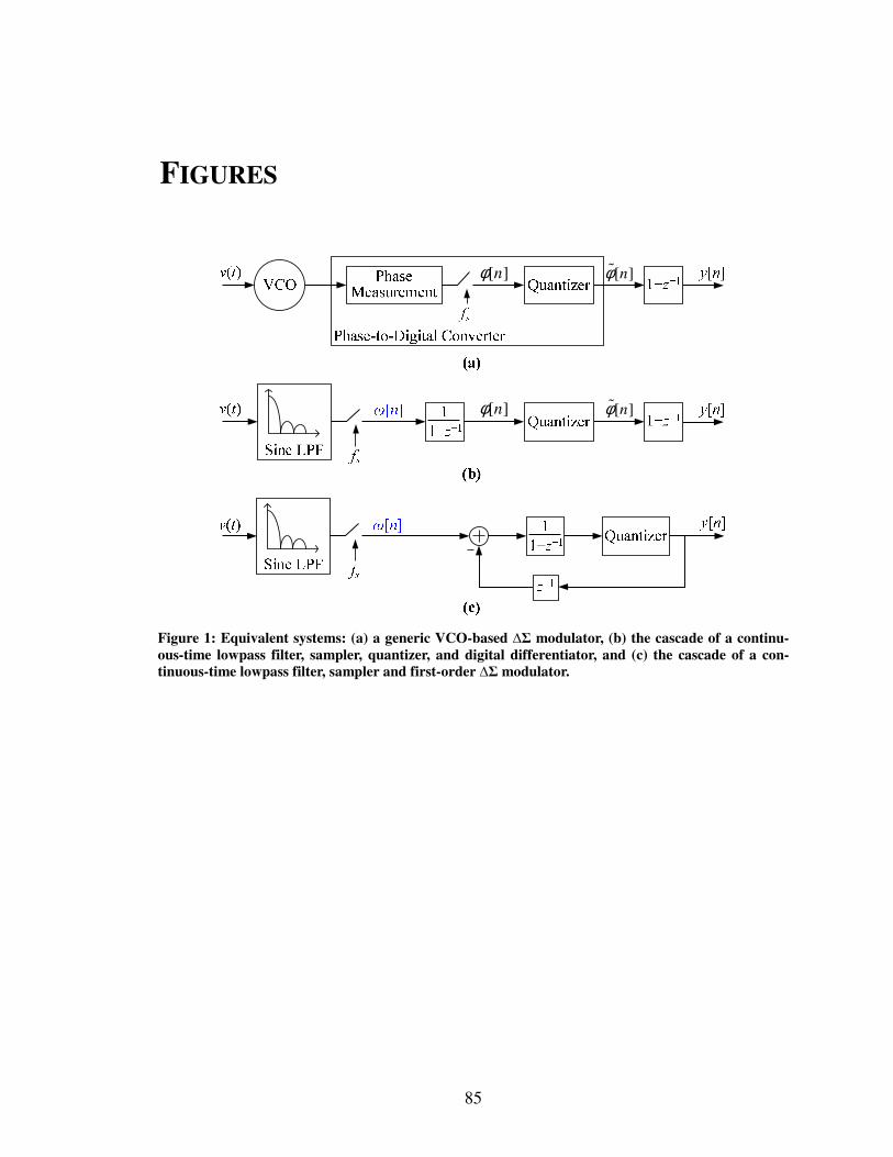
85
FIGURES
[ ]nφ [ ]nφɶ
[ ]nφ [ ]nφɶ
Figure 1: Equivalent systems: (a) a generic VCO-based ∆Σ modulator, (b) the cascade of a continu-
ous-time lowpass filter, sampler, quantizer, and digital differentiator, and (c) the cascade of a con-
tinuous-time lowpass filter, sampler and first-order ∆Σ modulator.
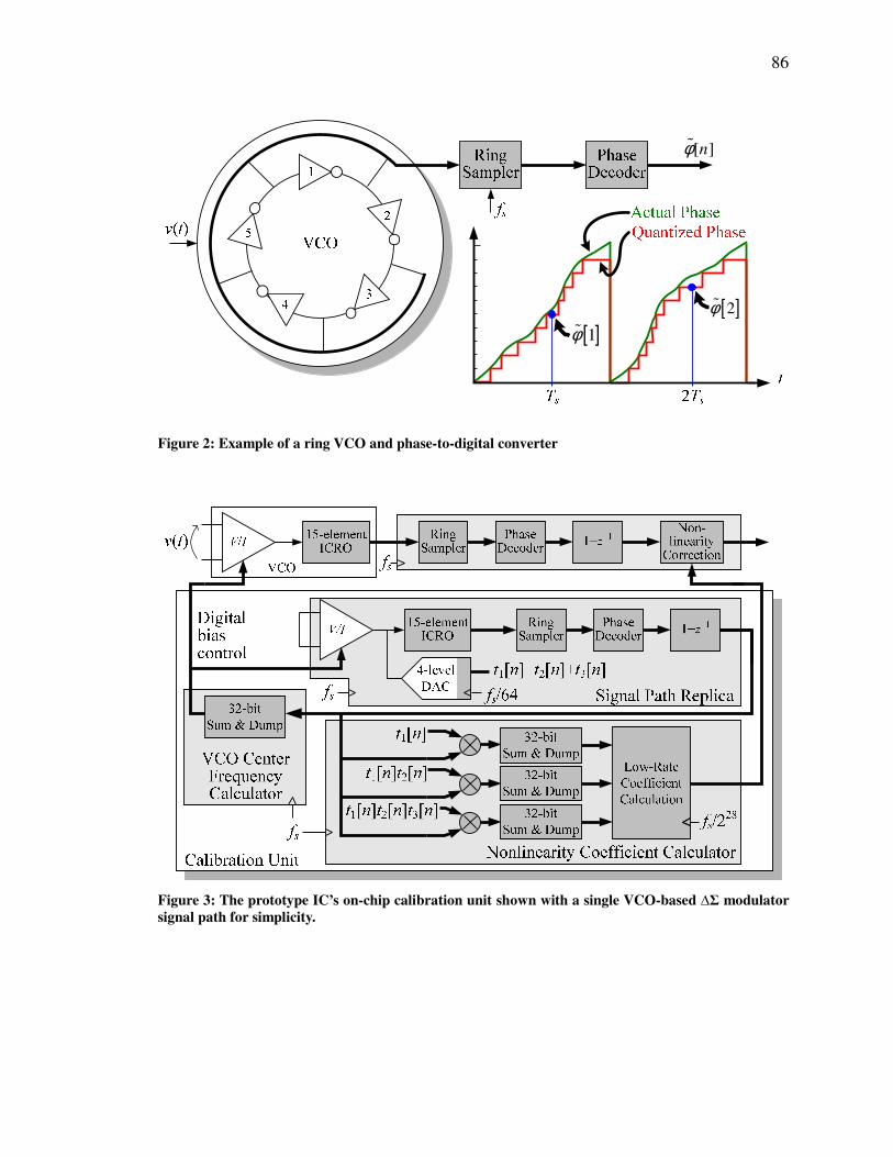
86
[ ]nφɶ
[ ]1φɶ[ ]2φɶ
Figure 2: Example of a ring VCO and phase-to-digital converter
Figure 3: The prototype IC’s on-chip calibration unit shown with a single VCO-based ∆Σ modulator
signal path for simplicity.
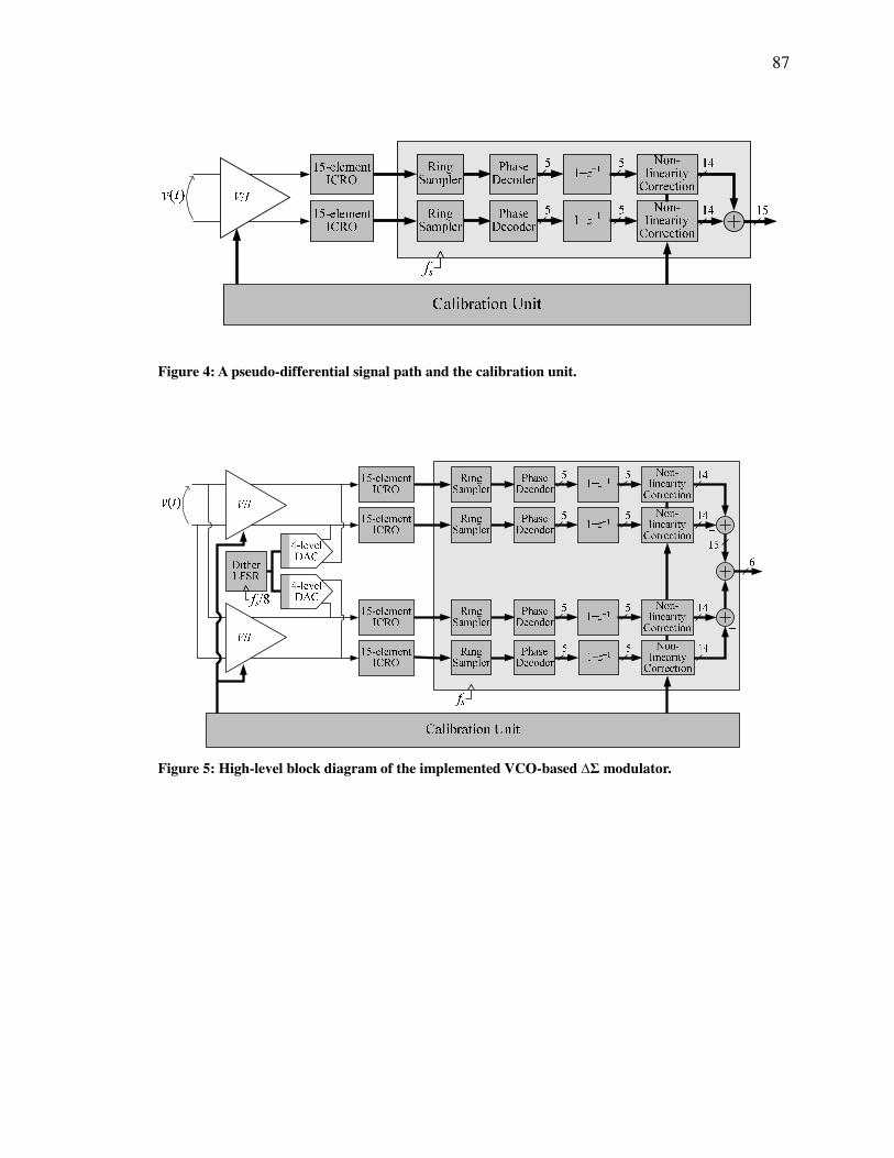
87
Figure 4: A pseudo-differential signal path and the calibration unit.
Figure 5: High-level block diagram of the implemented VCO-based ∆Σ modulator.

88
Figure 6: Example of the signal-dependent non-uniform quantization problem.
Figure 7: Example of the solution used to solve the signal-dependent non-uniform quantization prob-
lem.
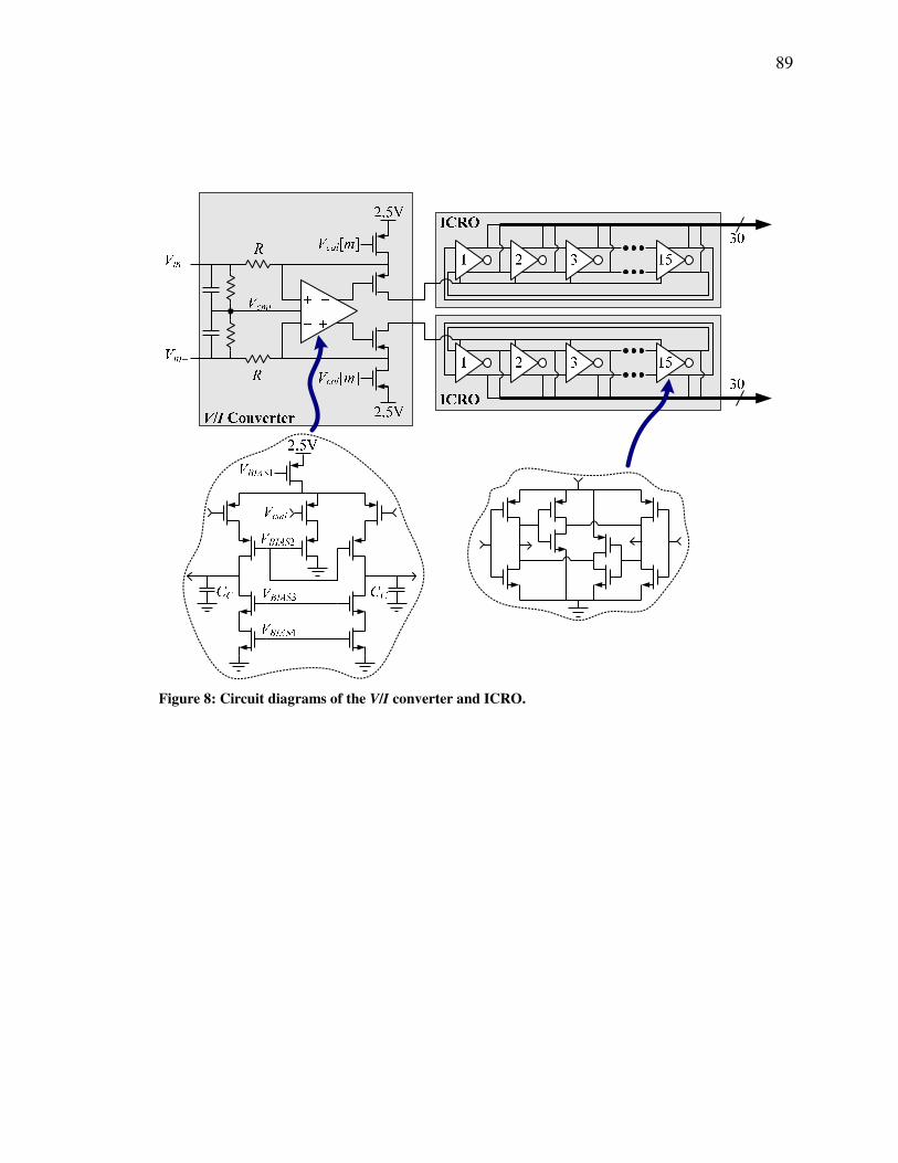
89
Figure 8: Circuit diagrams of the V/I converter and ICRO.
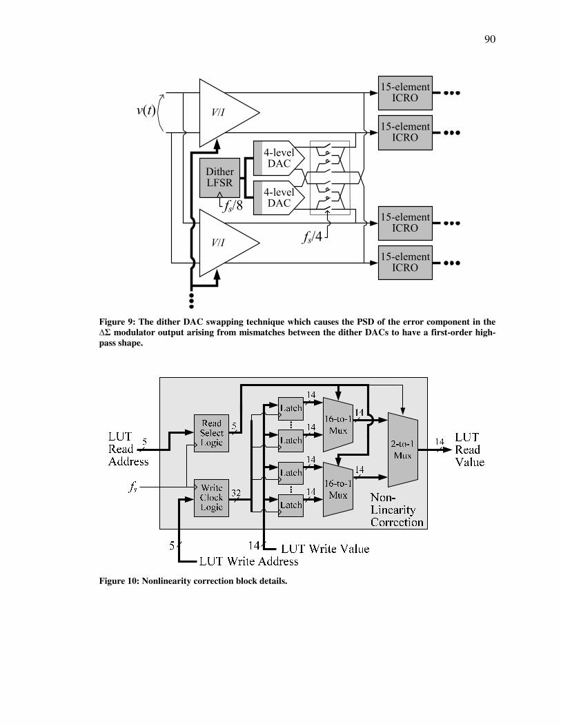
90
DitherLFSR
15-elementICRO
15-elementICRO
V/I
V/I
15-elementICRO
15-elementICRO
4-level DAC
4-level DACfs/8
v(t)
fs/4
Figure 9: The dither DAC swapping technique which causes the PSD of the error component in the
∆Σ modulator output arising from mismatches between the dither DACs to have a first-order high-
pass shape.
Figure 10: Nonlinearity correction block details.
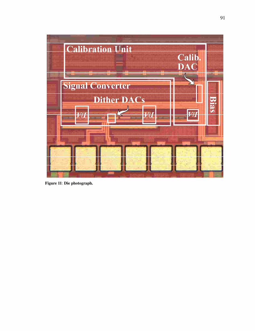
91
Figure 11: Die photograph.
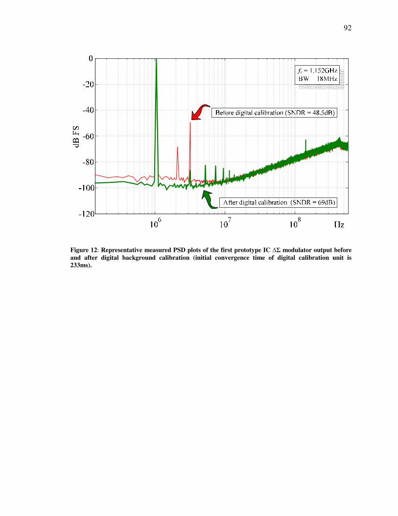
92
Figure 12: Representative measured PSD plots of the first prototype IC ∆Σ modulator output before
and after digital background calibration (initial convergence time of digital calibration unit is
233ms).
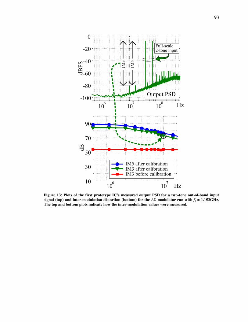
93
106
107
108
-100
-80
-60
-40
-20
0
Full-scale2-tone input
IM3
IM5
Hz
dBFS
Output PSD
10
30
50
70
90
106
107
Hz
IM5 after calibrationIM3 after calibrationIM3 before calibration
dB
Figure 13: Plots of the first prototype IC’s measured output PSD for a two-tone out-of-band input
signal (top) and inter-modulation distortion (bottom) for the ∆Σ modulator run with fs = 1.152GHz.
The top and bottom plots indicate how the inter-modulation values were measured.
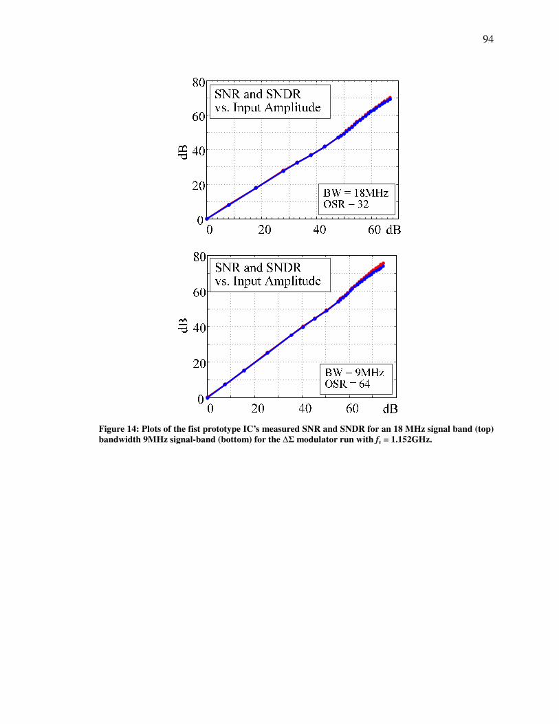
94
Figure 14: Plots of the fist prototype IC’s measured SNR and SNDR for an 18 MHz signal band (top)
bandwidth 9MHz signal-band (bottom) for the ∆Σ modulator run with fs = 1.152GHz.
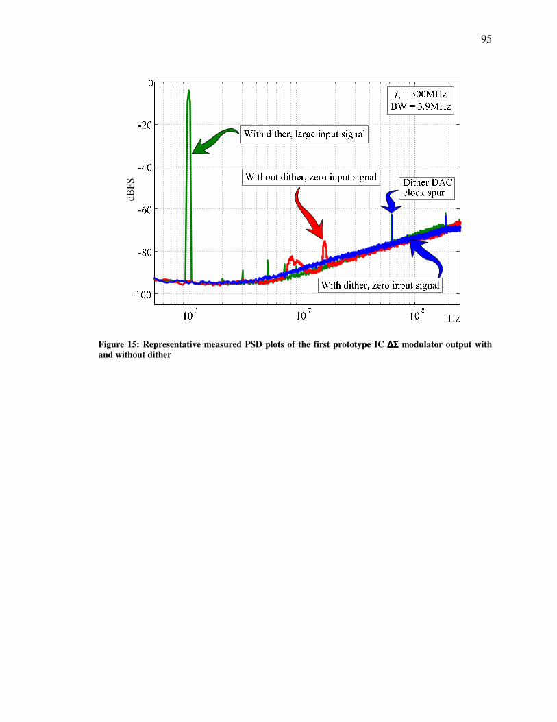
95
dBFS
Figure 15: Representative measured PSD plots of the first prototype IC ∆Σ∆Σ∆Σ∆Σ modulator output with
and without dither

96
ICRO30
(a)
ICRO14
(b)
(c)
28
ICRO
1 2 3 7
1 2 3 15
MP1 MP2
Figure 16: Circuit diagrams of various ICROs: (a) 15-element ICRO used in the first prototype IC,
(b) example 7-element ICRO, (c) dual, 7-element injection-locked ICRO used in the second prototype
IC
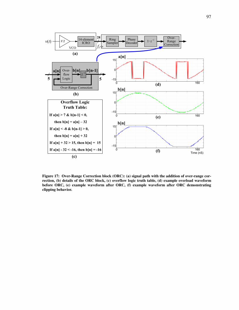
97
fs
RingSampler
1−z−1Phase
Decoderv(t)14-element
ICRO
VCO
Over-Range
Correction
(d)
(e)
(f)
Over-
flow
Logic5
Over-Range Correction
5
(b)
Overflow Logic
Truth Table:
If a[n] > 7 & b[n-1] < 0,
then b[n] = a[n] – 32
If a[n] < -8 & b[n-1] > 0,
then b[n] = a[n] + 32
If a[n] + 32 > 15, then b[n] = 15
If a[n] - 32 < -16, then b[n] = -16
V/I
28
(a)
(c)
a[n] b[n]z−1
b[n-1]
0 160 -8
-15
0
15
0 160
-15
0
15
0 160
-15
0
15
Time (nS)
a[n]
b[n]
b[n]
Figure 17: Over-Range Correction block (ORC): (a) signal path with the addition of over-range cor-
rection, (b) details of the ORC block, (c) overflow logic truth table, (d) example overload waveform
before ORC, (e) example waveform after ORC, (f) example waveform after ORC demonstrating
clipping behavior.

98
Figure 18: High-level block diagram of two VCO-based ∆Σ∆Σ∆Σ∆Σ modulators: (a) single pseudo-differential
modulator ADC with dither injected as a common-mode signal, (b) dual pseudo-differential modula-
tor ADC with dither injected as a differential signal.

99
Figure 19: V/I converter circuit diagrams: (a) first prototype IC V/I converter, (b) new open-loop V/I
converter

100
Calibration Unit
fs
RingSampler
PhaseDecoder
v(t)15-element
ICROV/I
Over-Range
Correction1−z−1
15-elementICRO
RingSampler
PhaseDecoder
t1[n]+t2[n]+t3[n]
Signal Path Replica
1−z−1
fs/64
4-level
DAC
fs
32-bit
Sum & Dump
VCO CenterFrequencyCalculator
t1[n]
t1[n]t2[n]t3[n]
t1[n]t2[n]
32-bit
Sum & Dump
32-bit
Sum & Dump
32-bit
Sum & Dumpfs/2
28
Nonlinearity Coefficient Calculator
Low-Rate
Coefficient
Calculation
VCO
Non-linearityCorrection
ADCDifferential
DriverCircuit
8-bit
DAC
V/I Input Common-
ModeVoltage
V/I
DummyV/I
Signal Path
Calibration Source
Figure 20: The second prototype IC’s on-chip calibration unit shown with a single VCO-based ∆Σ∆Σ∆Σ∆Σ
modulator signal path for simplicity
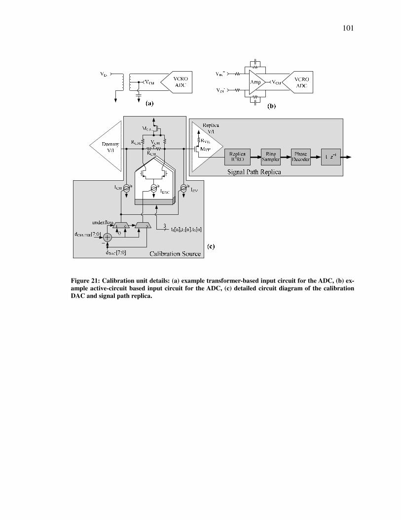
101
Figure 21: Calibration unit details: (a) example transformer-based input circuit for the ADC, (b) ex-
ample active-circuit based input circuit for the ADC, (c) detailed circuit diagram of the calibration
DAC and signal path replica.

102
Figure 22: Circuit diagrams of the ring sampler D-type flip-flops, (a) transmission-gate flip-flop used
in the first prototype that produces data-dependent hysteresis, (b) non-transmission-gate flip-flop
that is largely hysteresis free.
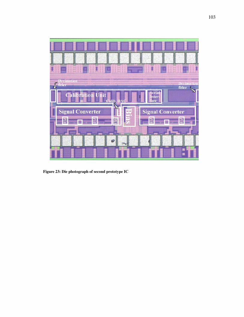
103
Figure 23: Die photograph of second prototype IC

104
105 106 107 108
-100
-80
-60
-40
-20
0
Freq (Hz)
dB FS
fs = 2.4GHz
BW = 18.75MHz
Before digital calibration
(SNDR = 50dB)
After digital calibration
(SNDR = 74dB)
1/f noise slope
-10dB/dec
Figure 24: Representative measured PSD plots of the second prototype IC ∆Σ∆Σ∆Σ∆Σ modulator output be-
fore and after digital background calibration
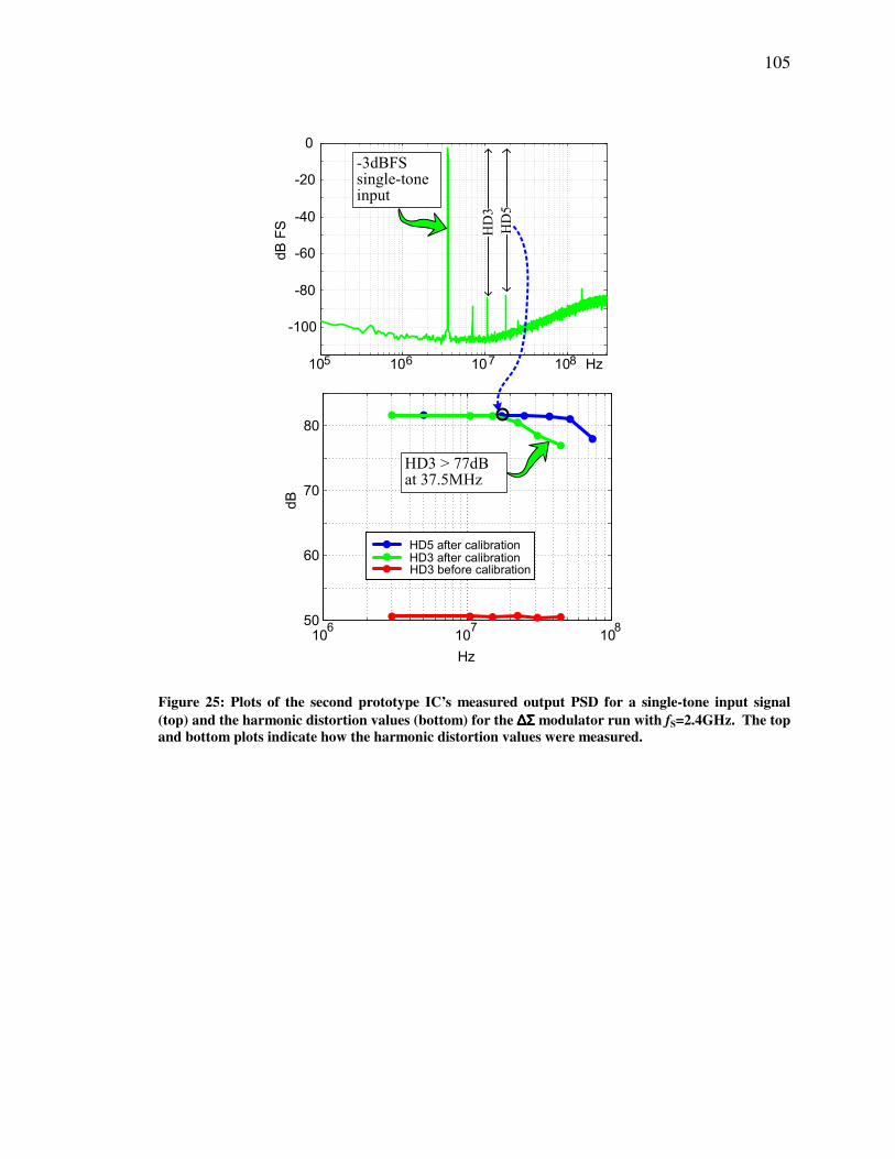
105
105 106 107 108
-100
-80
-60
-40
-20
0
Hz
dB FS HD5
HD3
-3dBFSsingle-tone input
Hz
106
107
108
50
60
70
80
dB
HD3 > 77dBat 37.5MHz
HD5 after calibrationHD3 after calibrationHD3 before calibration
Figure 25: Plots of the second prototype IC’s measured output PSD for a single-tone input signal
(top) and the harmonic distortion values (bottom) for the ∆Σ∆Σ∆Σ∆Σ modulator run with fS=2.4GHz. The top
and bottom plots indicate how the harmonic distortion values were measured.
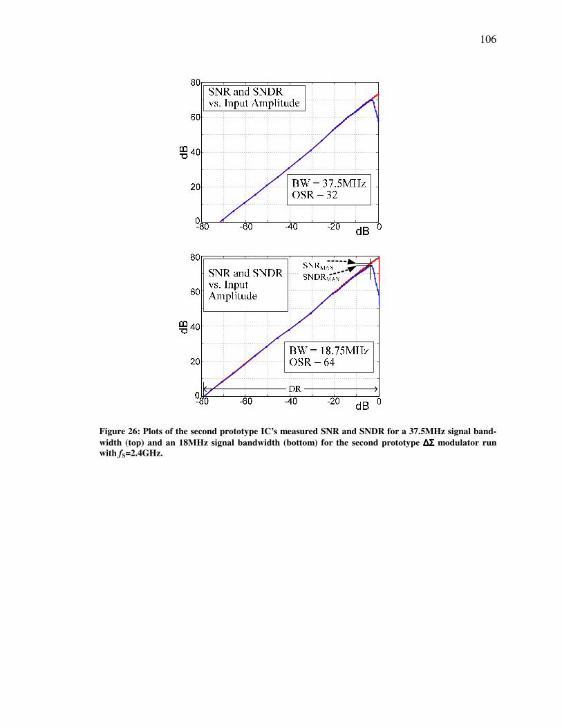
106
Figure 26: Plots of the second prototype IC’s measured SNR and SNDR for a 37.5MHz signal band-
width (top) and an 18MHz signal bandwidth (bottom) for the second prototype ∆Σ∆Σ∆Σ∆Σ modulator run
with fS=2.4GHz.
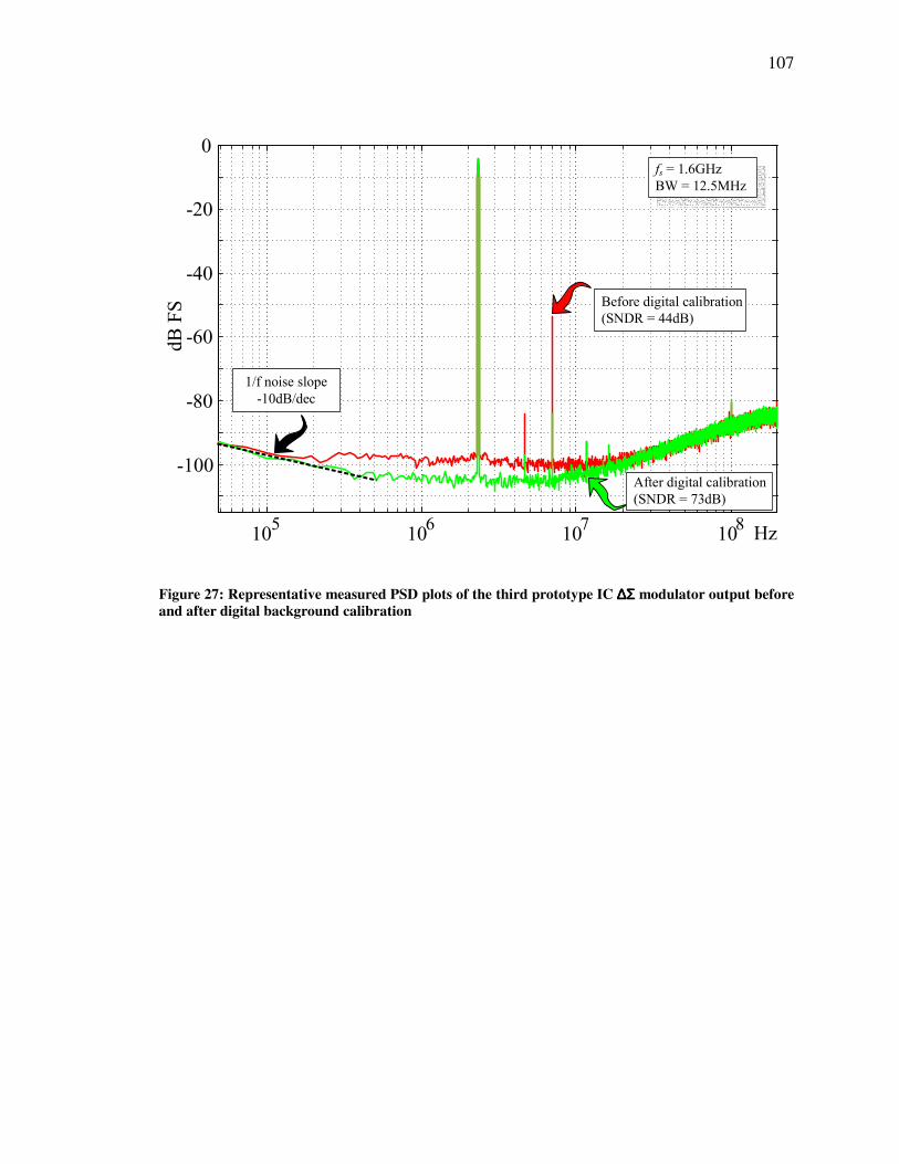
107
105
106
107
108
-100
-80
-60
-40
-20
0
Hz
dB FS Before digital calibration
(SNDR = 44dB)
fs = 1.6GHz
BW = 12.5MHz
After digital calibration
(SNDR = 73dB)
1/f noise slope
-10dB/dec
Figure 27: Representative measured PSD plots of the third prototype IC ∆Σ∆Σ∆Σ∆Σ modulator output before
and after digital background calibration
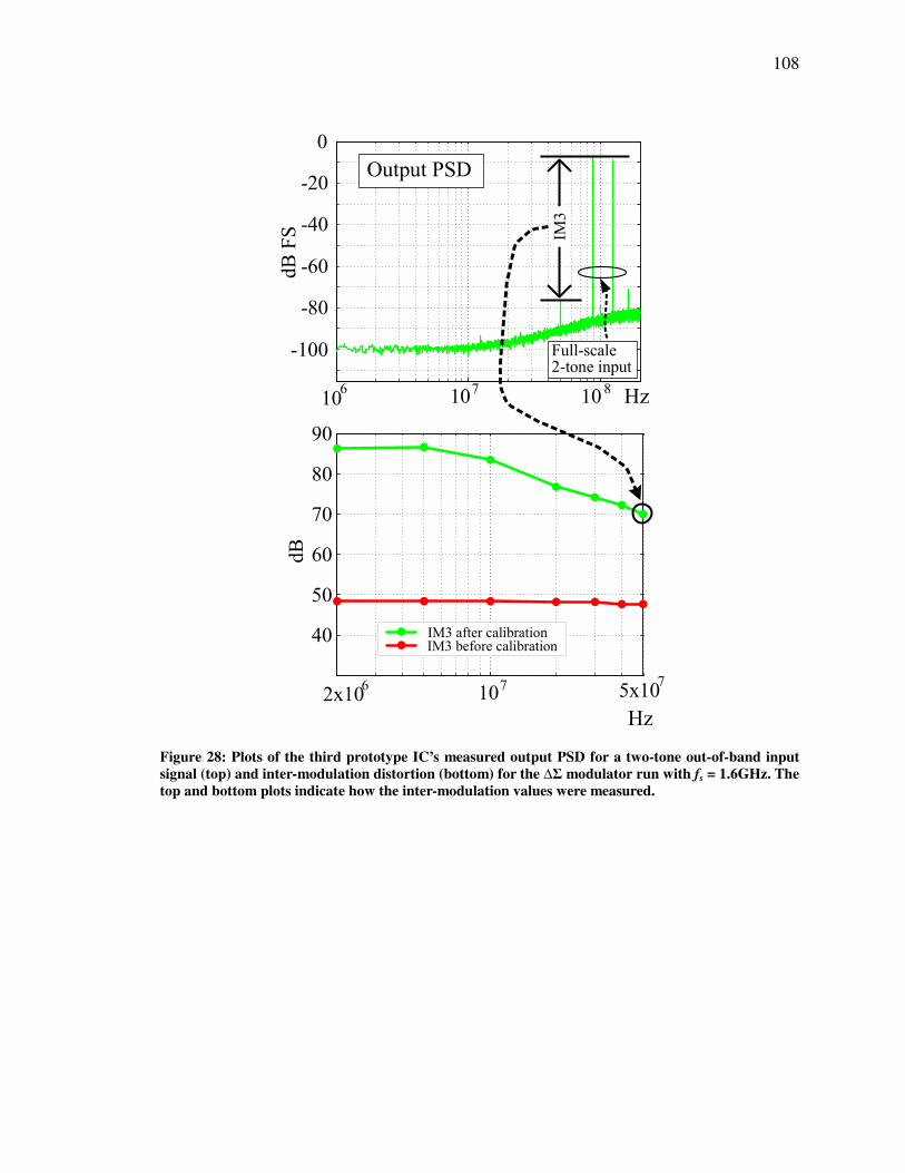
108
106
107
108
-100
-80
-60
-40
-20
0
dB FS
Hz
Full-scale2-tone input
IM3
Output PSD
40
50
60
70
80
90
dB
IM3 after calibrationIM3 before calibration
107 5x10
7
Hz2x10
6
Figure 28: Plots of the third prototype IC’s measured output PSD for a two-tone out-of-band input
signal (top) and inter-modulation distortion (bottom) for the ∆Σ modulator run with fs = 1.6GHz. The
top and bottom plots indicate how the inter-modulation values were measured.
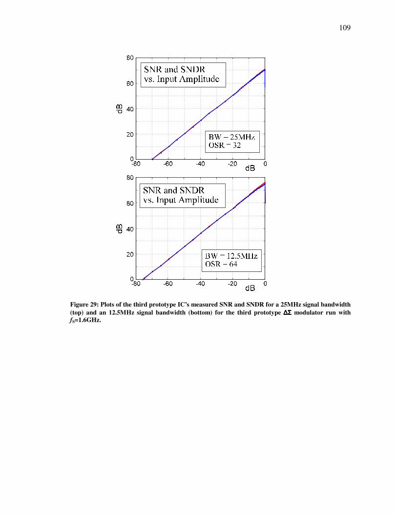
109
Figure 29: Plots of the third prototype IC’s measured SNR and SNDR for a 25MHz signal bandwidth
(top) and an 12.5MHz signal bandwidth (bottom) for the third prototype ∆Σ∆Σ∆Σ∆Σ modulator run with
fS=1.6GHz.
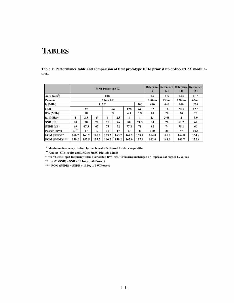
110
TABLES
Table 1: Performance table and comparison of first prototype IC to prior state-of-the-art ∆Σ modula-
tors.
Reference
[2]
Reference
[3]
Reference
[4]
Reference
[5]
Area (mm2) 0.7 1.5 0.45 0.15
Process 180nm 130nm 130nm 65nm
fS (MHz) 500 640 640 900 250
OSR 128 64 32 16 22.5 12.5
BW (MHz) 4.5 3.9 10 20 20 20
fIN (MHz)* 1 2.3 5 1 2.3 1 1 2.4 3.68 2 3.9
SNR (dB) 70 70 70 76 76 80 71.5 84 76 81.2 62
SNDR (dB) 69 67.3 67 73 72 77.8 71 82 74 78.1 60
Power (mW) 17 ++
17 17 17 17 17 8 100 20 87 10.5
FOM (SNR)** 160.2 160.2 160.2 163.2 163.2 164.2 158.4 164.0 166.0 164.8 154.8
FOM (SNDR)*** 159.2 157.5 157.2 160.2 159.2 162.0 157.9 162.0 164.0 161.7 152.8
+ Maximum frequency limited by test board FPGA used for data acquisition
++
Analog (V/I circuits and DACs): 5mW, Digital: 12mW
* Worst-case input frequency value over stated BW (SNDR remains unchanged or improves at higher fIN values
** FOM (SNR) = SNR + 10 log10(BW/Power)
*** FOM (SNDR) = SNDR + 10 log10(BW/Power)
32 64
18 9
65nm LP
0.07
First Prototype IC
1152+
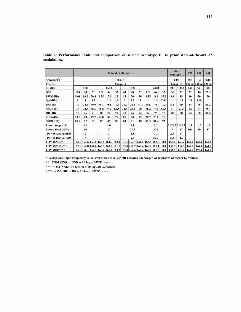
111
Table 2: Performance table and comparison of second prototype IC to prior state-of-the-art ∆Σ
modulators.
[2] [3] [4]
Area (mm2) 0.7 1.5 0.45
Process 180nm 130nm 130nm
fS (MHz) 500 1152 640 640 900
OSR 128 64 32 128 64 32 64 48 32 128 64 32 64 32 32 16 22.5
BW (MHz) 5.08 10.2 20.3 6.25 12.5 25 15 20 30 9.38 18.8 37.5 3.9 18 10 20 20
fIN (MHz)* 1 1 3.5 1 2.3 4.9 2 3.5 5 1 3.5 7.49 1 2.3 2.4 3.68 2
SNR (dB) 77 74.5 69.9 78.1 75.8 70.3 75.7 74.1 71.1 79.8 76 70.4 71.5 70 84 76 81.2
SNDR (dB) 75 72.7 68.5 76.8 74.3 69.8 74.6 73.1 70 76.2 74.1 69.8 71 67.3 82 74 78.1
DR (dB) 78 76 71 80 77 72 78 76 72 82 78 73 70 68 84 80 81.2
THD (dB) 79.6 79 79.2 82.8 82 79 81 80 77 78.7 78.6 76
SFDR (dB) 81.8 82 82 85 85 80 84 81 78 81.3 81.4 77
Power Supply (V) 2.5/1.2 2.5/1.2 1.8 1.2 1.2
Power Total (mW) 8 17 100 20 87
Power Analog (mW) 2.5 5
Power Digital (mW) 5.5 12
FOM (SNR)** 164.1 164.6 163.0 163.8 164.5 162.0 163.1 162.7 161.5 163.8 163.0 160 158.4 160.2 164.0 166.0 164.8
FOM (SNDR)*** 162.1 162.8 161.6 162.5 163.0 161.5 162.0 161.7 160.4 160.2 161.1 160 157.9 157.5 162.0 164.0 161.7
FOM (DR)**** 165.1 166.1 164.1 165.7 165.7 163.7 165.4 164.6 162.4 166.0 165.0 163 156.9 158.2 164.0 170.0 164.8
* Worst-case input frequency value over stated BW (SNDR remains unchanged or improves at higher fIN values)
** FOM (SNR) = SNR + 10 log10(BW/Power)
*** FOM (SNDR) = SNDR + 10 log10(BW/Power)
**** FOM (DR) = DR + 10 log10(BW/Power)
0.07
65nm LP
First
Prototype ICSecond Prototype IC
7.2
30.3
0.9
10 27.517
1.11.0 1.2
37.5
1300 1600
0.075
65nm G+
1920 2400
4.5
23
2
8
3
14

112
Table 3: Performance table and comparison of third prototype IC fabricated in 65nm LP process to
first IC fabricated in 65nm G+ process
Area (mm2)
Process
fS (MHz) 500
OSR 128 64
BW (MHz) 4.5 3.9
fIN (MHz)* 1 2.3 5 * 1 2.3 * 1 1 4.9 *
SNR (dB) 70 70 70 76 76 80 71.5 71.5
SNDR (dB) 69 67.3 67 73 72 77.8 71 69.9
Power Supply (V) 2.5/1.2 2.5/1.2 2.5/1.2 2.5/1.2 2.5/1.2 2.5/1.2 2.5/1.2 1.0
Power (mW) 17 17 17 17 17 17 8 20
Analog Power(mW) 5 5 5 5 5 5 2.5 6
Digital Power (mW) 12 12 12 12 12 12 5.5 14
FOM (SNR)** 160.2 160.2 160.2 163.2 163.2 164.2 158.4 162.5
FOM (SNDR)*** 159.2 157.5 157.2 160.2 159.2 162.0 157.9 160.9
* Worst-case input frequency value over stated BW (SNDR remains unchanged or improves at higher fIN values
** FOM (SNR) = SNR + 10 log10(BW/Power)
*** FOM (SNDR) = SNDR + 10 log10(BW/Power)
6
14
162.5
161.5
2.3
71.5
70.5
20
6
14
165.0
162.0
2.3 *
77
74
20
First Prototype IC
1152
32 64
65nm LP
0.07
18 9
1.0 1.0
Third Prototype IC
0.075
65nm G+
1600
32
25
64
12.5
113
REFERENCES
1. R. Schreier, G. C. Temes, Understanding Delta-Sigma Data Converters, John
Wiley and Sons, 2005.
2. W. Yang, W. Schofield, H. Shibata, S. Korrapati, A. Shaikh, N. Abaskharoun, D.
Ribner, “A 100mW 10MHz-BW CT ∆Σ Modulator with 87dB DR and 91dBc
IMD”, IEEE International Solid-State Circuits Conference, pp. 498-499, Febru-
ary 2008.
3. G. Mitteregger, C. Ebner, S. Mechnig, T. Blon, C. Holugigue, E. Romani, “A 20-
mW 640-MHz CMOS Continuous-Time ∆Σ ADC With 20-MHz Signal Band-
width, 80-dB Dynamic Range and 12-bit ENOB,” IEEE Journal of Solid-State
Circuits, vol. 41, no. 12, pp. 2641-2649, December 2006.
4. M. Park, M. Perrott, “A 0.13µm CMOS 78dB SNDR 87mW 20MHz BW CT ∆Σ
ADC with VCO-Based Integrator and Quantizer,” IEEE International Solid-State
Circuits Conference, pp. 170-171, February 2009.
5. V. Dhanasekaran, M. Gambhir, M. M. Elsayed, E. Sánchez-Sinencio, J. Silva-
Martinez, C. Mishra, L. Chen, E. Pankratz, “A 20mHz BW 68dB DR CT ∆Σ
ADC Based on a Multi-Bit Time-Domain Quantizer and Feedback Element,”
IEEE International Solid-State Circuits Conference, pp. 174-175, February 2009.
6. M. Høvin, A. Olsen, T. S. Lande, C. Toumazou, “Delta-Sigma Modulators Using
Frequency-Modulated Intermediate Values,” IEEE Journal of Solid-State Cir-
cuits, vol. 32, no. 1, pp. 13-22, Jan. 1997.
7. J. Kim, S. Cho, “A Time-Based Analog-to-Digital Converter Using a Multi-
Phase Voltage- Controlled Oscillator,” IEEE International Symposium on Cir-
cuits and Systems, pp. 3934-3937, May 2006.

114
8. R. Naiknaware, H. Tang, T. Fiez, “Time-Referenced Single-Path Multi-Bit ∆Σ
ADC using a VCO-Based Quantizer,” IEEE Transactions on Circuits and Sys-
tems – II: Analog and Digital Signal Processing, vol. 47, no. 7, pp. 596-602, July
2000.
9. A. Iwata, N. Sakimura, M. Nagata, T. Morie, “The Architecture of Delta Sigma
Analog-to-Digital Converters Using a Voltage-Controlled Oscillator as a Multibit
Quantizer,” IEEE Transactions on Circuits and Systems – II: Analog and Digital
Signal Processing, vol. 46, no. 7, pp. 941-945, July 1999.
10. U. Wismar, D. Wisland, P. Andreani, “A 0.2 V, 7.5 µW, 20 kHz Σ∆ modulator
with 69 dB SNR in 90 nm CMOS,” European Solid-State Circuits Conference,
pp. 206-209, September 2007.
11. F. Opteynde, “A Maximally-Digital Radio Receiver Front-End,” IEEE Interna-
tional Solid-State Circuits Conference, pp. 450-451, February 2010.
12. M. Z. Straayer, M. H. Perrott, “A 12-Bit, 10-MHz Bandwidth, Continuous-Time
Σ∆ ADC With a 5-Bit, 950-MS/s VCO-Based Quantizer,” IEEE Journal of Solid-
State Circuits, vol. 43, no. 4, April 2008.
13. I. Galton, G. Taylor, “A Mostly Digital Variable-Rate Continuous-Time ADC ∆Σ
Modulator,” IEEE International Solid-State Circuits Conference, pp. 298-299,
February, 2010.
14. A. Panigada, I. Galton, “Digital Background Correction of Harmonic Distortion
in Pipelined ADCs,” Circuits and Systems - I: Regular Papers, IEEE Transac-
tions on, vol. 53, no. 9, pp. 1885-1895, September 2006.
15. Panigada, I. Galton, “A 130 mW 100 MS/s Pipelined ADC with 69 dB SNDR
Enabled by Digital Harmonic Distortion Correction,” IEEE Journal of Solid-
State Circuits, vol. 44, no. 12, pp. 3314-3328, December 2009.
16. I. Galton, “Granular Quantization Noise in a Class of Delta-Sigma Modulators,”
IEEE Transactions on Information Theory, vol. 40, no. 3, pp. 848-859, May
1994.
115
17. A. B. Sripad, D. L. Snyder, “A Necessary and Sufficient Condition for Quantiza-
tion Errors to be Uniform and White,” IEEE Transactions on Acoustics, Speech,
and Signal Processing, vol. ASSP-25, no. 5, pp. 442-448, October 1977.
18. R. Adams, K. Nguyen, K. Sweetland, “A 113dB SNR Oversampling DAC with
Segmented Noise-Shaped Scrambling,” IEEE International Solid-State Circuits
Conference, pp. 62-63, 413, February, 1998.
19. B. Boser, K.-P. Karmann, H. Martin, B. Wooley, “Simulating and Testing Over-
sampled Analog-to-Digital Converters”, IEEE Transactions on Computer Aided
Design, Vol. 7, No. 6, pp. 668-674, June 1988.
20. N. Maghari, Un-Ku Moon, “A Third-Order DT DS Modulator Using Noise-
Shaped Bidirectional Single-Slope Quantizer,” IEEE International Solid-State
Circuits Conference, pp. 474-476, February, 2011.
21. M. Bolatkale, L.J. Breems, R. Rutten, K.A.A. Makinwa, “A 4GHz CT DS ADC
with 70dB DR and -74dBFS THD in 125MHz BW,” IEEE International Solid-
State Circuits Conference, pp. 470-472, February, 2011.