United States Patent Patent Number: 5,436,452 d. Date …. Pat. No. 5,258,748 TECHNICAL FIELD 15 The...
15
I 11111 111 l l 1111111111111111 I l l 11 11111 11111 11111 11111 I l l 11 111111 111 11111 1111 United States Patent 1191 US005436452A [ill Patent Number: 5,436,452 Kenny et d. [45] Date of Patent: Jul. 25, 1995 r54i UNCOOLED TUNNELJHG INFRARED - - SENSOR [75] Inventors: [73] Assignee: [21] Appl. NO.: [22] Filed: Thomas W. Kenny, Glendale; William J. Kaiser, West Covina; Judith A. Podosek, Arcadia; Erika C. Vote, Pasadena; Richard E. Muller, Sunland; Paul D. Maker, Arcadia, all of Calif. California Institute of Technology, Pasadena, Calif. 79,507 Jun. 21,1993 Related U.S. Application Data [63] Continuation-in-part of Ser. No. 898,682, Jun. 15,1992, Pat. No. 5,298,748. [51] In& Cl.6 .......................... GOlJ 5/00; HOlJ 37/00 [52] U.S. Cl. .................................. 250/338.1; 250/306 [58] Field of Search .................. 250/338.1,306,423 F 1561 References Cited U.S. PATENT DOCUMENTS 3,887,937 6/1975 Gatos et al. .................... 250/370.14 4,906,840 3/1990 Zdeblick et al. .................... 250/307 5,043,577 8/1991 Pohl et al. ........................... 250/306 5,051,379 9/1991 Bager et al. ............................. 437/8 5,103,174 4/1992 Wandass et al. .................... 324/209 5,265,470 11/1993 Kaiser et al. ...................... 73/178 R 5,290,102 3/1994 Kaiser et al. ........................ 324/120 5,298,748 3/1994 Kenny .............................. 250/338.1 Primary Examiner-Bruce C. Anderson Attorney, Agent, or Firm-Leonard Tachner 1571 ABSTRACT An uncooled infrared tunneling sensor in which the only moving part is a diaphragm which is deflected into contact with a micromachined silicon tip electrode prepared by a novel lithographic process. Similarly prepared deflection electrodes employ electrostatic force to control the deflection of a silicon nitride, flat diaphragm membrane. The diaphragm exhibits a high resonant frequency which reduces the sensor’s sensitiv- ity to vibration. A high bandwidth feedback circuit controls the tunneling current by adjusting the deflec- tion voltage to maintain a constant deflection of the membrane. The resulting infrared sensor can be minia- turized to pixel dimensions smaller than 100 pm. An alternative embodiment is implemented using a c o m - gated membrane to permit large deflection without complicated clamping and high deflection voltages. The alternative embodiment also employs a pinhole aperture in a membrane to accommodate environmental temperature variation and a sealed chamber to eliminate environmental contamination of the tunneling elec- trodes and undesireable accoustic coupling to the sen- sor. 19 Claims, 7 Drawing Sheets PINHOLE \ MEMBRANE \TIP https://ntrs.nasa.gov/search.jsp?R=20080004763 2018-06-27T20:47:32+00:00Z
Transcript of United States Patent Patent Number: 5,436,452 d. Date …. Pat. No. 5,258,748 TECHNICAL FIELD 15 The...

I11111 111ll1111111111111111 Ill11 11111 11111 11111 11111 Ill11 111111 111 11111 1111 United States Patent 1191
US005436452A [ill Patent Number: 5,436,452
Kenny et d. [45] Date of Patent: Jul. 25, 1995
r54i UNCOOLED TUNNELJHG INFRARED - - SENSOR
[75] Inventors:
[73] Assignee:
[21] Appl. NO.:
[22] Filed:
Thomas W. Kenny, Glendale; William J. Kaiser, West Covina; Judith A. Podosek, Arcadia; Erika C. Vote, Pasadena; Richard E. Muller, Sunland; Paul D. Maker, Arcadia, all of Calif.
California Institute of Technology, Pasadena, Calif. 79,507
Jun. 21,1993
Related U.S. Application Data [63] Continuation-in-part of Ser. No. 898,682, Jun. 15,1992,
Pat. No. 5,298,748.
[51] In& Cl.6 .......................... GOlJ 5/00; HOlJ 37/00 [52] U.S. Cl. .................................. 250/338.1; 250/306 [58] Field of Search .................. 250/338.1, 306, 423 F 1561 References Cited
U.S. PATENT DOCUMENTS 3,887,937 6/1975 Gatos et al. .................... 250/370.14 4,906,840 3/1990 Zdeblick et al. .................... 250/307 5,043,577 8/1991 Pohl et al. ........................... 250/306 5,051,379 9/1991 Bager et al. ............................. 437/8 5,103,174 4/1992 Wandass et al. .................... 324/209 5,265,470 11/1993 Kaiser et al. ...................... 73/178 R
5,290,102 3/1994 Kaiser et al. ........................ 324/120 5,298,748 3/1994 Kenny .............................. 250/338.1
Primary Examiner-Bruce C. Anderson Attorney, Agent, or Firm-Leonard Tachner
1571 ABSTRACT An uncooled infrared tunneling sensor in which the only moving part is a diaphragm which is deflected into contact with a micromachined silicon tip electrode prepared by a novel lithographic process. Similarly prepared deflection electrodes employ electrostatic force to control the deflection of a silicon nitride, flat diaphragm membrane. The diaphragm exhibits a high resonant frequency which reduces the sensor’s sensitiv- ity to vibration. A high bandwidth feedback circuit controls the tunneling current by adjusting the deflec- tion voltage to maintain a constant deflection of the membrane. The resulting infrared sensor can be minia- turized to pixel dimensions smaller than 100 pm. An alternative embodiment is implemented using a com- gated membrane to permit large deflection without complicated clamping and high deflection voltages. The alternative embodiment also employs a pinhole aperture in a membrane to accommodate environmental temperature variation and a sealed chamber to eliminate environmental contamination of the tunneling elec- trodes and undesireable accoustic coupling to the sen- sor.
19 Claims, 7 Drawing Sheets
PINHOLE \
MEMBRANE \TIP
https://ntrs.nasa.gov/search.jsp?R=20080004763 2018-06-27T20:47:32+00:00Z

U.S. Patent July 25,1995 Sheet 1 of 7 5,436,452
WINDOW
FIG. 1
FIG. 2

U.S. Patent July 25,1995
a W > W g 4
Sheet 2 of 7 5,436,452
z g
P W -I LL W
cj L L

U.S. Patent July 25, 1995 Sheet 3 of 7 5,436,452
-
-15V
1
FIG. 5

U.S. Patent
2 .o I .8 1.6 I .4 I .2 1.0
0.8
0.6
0.4
0.2
July 25,1995 Sheet 4 of 7 5,436,452
to3 io4
FREQUENCY (Hz)
lo5 IO6
FIG. 6
US. Patent July 25, 1995 Sheet 5 of 7
PHASE SHIFT
FREQUENCY Wz)
5,436,452
FIG. 7
U.S. Patent July 25,1995 Sheet 6 of 7 5,436,452
FIG. 8
PINHOLE \
I MEMBRANE
FIG. 9

U.S. Patent
WIRE TO PREAMP
July 25,1995 Sheet 7 of 7 5,436,452
TIP \
FIG. 10
FIG. 11
1 5,436,452
UNCOOLED TUNNELING INFRARED SENSOR
ORIGIN OF INVENTION The invention described herein was made in the per-
formance of work under a NASA contract, and is sub- ject to the provisions of Public Law 96-517 (35 USC 202) in which the Contractor has elected to retain title.
CROSS-REFERENCE TO RELATED APPLI- CATION 10
This application is a continuation-in-part of applica- tion Ser. No. 07/898,682 filed on Jun. 15, 1992, now US. Pat. No. 5,258,748
TECHNICAL FIELD 15 The present invention relates generally to infrared
sensors and more specifically to a tunneling transducer having a membrane within tunneling distance of a mi- cromachined tip and having a feedback circuit to elec- trostatically retain that distance despite infrared energy- 20 induced mechanical forces whereby the feedback cir- cuit provides quantification of incident infrared energy.
BACKGROUNDART.
are becoming increasingly important for a variety of Instruments for the measurement of infrared radiation 25
commercial and non-commercial applications. -Re- search into the development of uncooled sensors with response throughout the infrared spectrum has become particularly important due to the limitations on the operation of cooling systems. Uncooled infrared sensors would have important applications for space-based remote-sensing of thermal sources, night vision, target identification, thermal mapping, event detection, mo- tion detection, and others. The limitations of the perfor- mance of the existing uncooled sensors often are the primary constraint to the performance of infrared imag- ing systems for many applications. As a result, there has been considerable investment in the development of uncooled infrared sensors.
A broad assortment of infrared detectors has been developed, over the last 40 years. In most cases, they may be classified as either quantum or thermal detec- tors, depending upon whether the incoming radiation is converted to excitations which are collected, or is converted to heat and detected through changes in temperature. In general, a quantum detector which operates at detector temperature Td is usually superior to a thermal detector at the same temperature for infrared frequencies: hv> >bTd, where h is Planck’s constant and 1(8 is Boltzmann’s constant. However, for infrared frequencies: hv< <bTd, thermal detectors represent the only functional technology. The oper- ation of quantum detectors is limited by the availability of efficient photon conversion mechanisms, while the operation of thermal detectors is limited by the avail- ability of sensitive thermometers. Only thermal infrared sensors operate in the mid-to-far infrared (A> 10p.m) and at room temperature.
The pneumatic infrared detector, which was origi- nally developed by Golay, is classified as a thermal detector. Golay’s detector consisted of a small cavity filled with gas at room temperature. The cavity is separated from the surroundings by a window and a thin, flexible membrane. The membrane was coated on one side with a thin metallic film, which has significant absorption throughout the infrared spectrum whenever the sheet resistance of the film is approximately half of
30
i5
40
45
50
55
60
65
2 the impedance of free space. The trapped gas in the Golay cell was heated by contact with the membrane and expanded thermally, which forced the membrane to deflect outward. This deflection is usually detected with optical or capacitive displacement transducers. At present, these detectors are bulky, fragile, difficult to fabricate, and expensive. Nevertheless, they have been widely used, primarily because of their improvement in sensitivity over all other room-temperature detectors in the mid to far infrared range. Attempts to miniaturize the Golay cell for incorporation into focal plane arrays have been unsuccessful because of scaling laws which relate the sensitivity of conventional displacement transducers and their active area. The need for focal- plane arrays of uncooled detectors stimulated the de- velopment of pyroelectric detector arrays, the best of which are 5-10 times less sensitive than the Golay cell.
With the above considerations in mind, the present invention is based on the development of an improved Golay cell. This new sensor is constructed entirely from micromachined silicon components. To detect the mo- tion of the membrane, the invention uses an electron tunneling displacement transducer. This sensor, like the assemblies used in Scanning Tunneling Microscopy (STM), detects electrons which tunnel through the classically forbidden barrier between a tip and a surface. As in the STM, the electron current is exponentially dependent on the separation between the tip and the surface. Through use of the electron tunneling trans- ducer, the scaling laws which have prevented the minia- turization of the Golay cell are avoided.
Any new developments in transducer technology that avoid the constraints which relate to the sensitivity and dimensions of classical displacement transducers are very important. The STM, which was invented by G. Binnig and H. Rohrer of IBM Zurich and won the 1986 Nobel Prize in Physics, is based on the measure- ment of electron tunnel current between a surface of interest and a sharp tip, while the tip i s raster-scanned across the surface. This device is capable of resolving atomic-scale structure on the surface of interest and has enabled many pioneering discoveries of the structure, and behavior of atoms at surfaces. The most important element of STM is the measurement of tunneling cur- rent between the tip and substrate. The tunneling cur- rent, I, has the following dependence on the separation, s, between a pair of metallic electrodes:
I a VexH- a% s),
where is the height of the tunneling barrier and V is the bias voltaee; V is the small compared to @, and ?=1.025 (A-1 eV- f ) .For typca lva luero f~=5 ev and s=7 A, the curroent varies by nearly an order of magnitude for each 1 A change in electrode separation. This sensi- tivity to relative position is superior to that available in all conventional compact transducers. Since tunnelby only occurs in regions where the tip is within several A of the surface, the active area of the sensor is micro- scopic. The use of electron tunneling as the active ele- ment of a displacement transducer for generic sensor purposes has been pioneered at the Jet Propulsion Lab- oratory (JPL) over the last several years resulting in the construction of a series of proof-of-concept prototypes. These prototypes initially were constructed from a variety of materials, and served to illustrate that, if

5,436,452 3 4
designed properly, tunneling could be used in a dis- placement transducer.
STATEMENT OF THE INVENTION
red tunneling Sensor in which the only moving part is a membrane which is deflected into contact with a mi- cromachined silicon tip electrode prepared by a novel lithographic process. Similarly prepared deflection BRIEF DESCRIPTION OF THE DRAWING electrodes employ electrostatic force to control the lo
The membrane exhibits a &,h resonant frequency present invention, as well as additional objects and ad- vantages thereof, will be more fully understood herein- which reduces the sensor's sensitivity to vibration. A after as a result of a detailed description of a preferred wide bandwidth feedback circuit controls the tunneling 15 embodiment when taken in conjunction with the fol-
current by adjusting the deflection voltage to maintain lowing drawings in which: a constant deflection of the membrane which would infrared sensor otherwise change deflection depending upon incident demonstrating the concept of using a tunneling dis- infrared radiation. The resulting infrared sensor can placement transducer to deflection of a mem- meet Or exceed the performance Of alI Other 20 brane driven by infrared-induced expansion of trapped
gas; uncooled, infrared sensors and can be miniaturized to pixel dimensions of 100 Pm- The technOIOgY can be FIG. 2 is a graph illustrating noke sources affecting readily implemented as a small-format linear array suit- infrared detector sensitivity; able for commercial and spacecraft applications. One FIG. 3 is a conceptual drawing of a prototype trans- m~bodiment of the invention is implemented with a 25 ducer used to demonstrate the concept of the present number of further improvements which enable simpli- fied fabrication and more routine operation without FIG. 4 is a conceptual drawing ofthe tunneling infra- complicating non-ideal characteristics enountered in earlier embodiments. These improvements include: Use FIG. 5 is a schematic drawing of the infrared Sensor of a corrugated diaphragm to increase flexibility over a 30 of the invention including a feedback circuit used to larger deflection range; use of a membrane pinhole control the tunneling transducer; aperture to eliminate dc-sensitivity of the sensor to FIG. 6 is a graph of the ratio of measured to reference environmental temperature variations; and use of a oscillations in the tunneling current as a function of sealed chamber with a silicon wafer as an infrared win- frequency demonstrating a bandwidth measurement of dow to eliminate environmental contamination of the 35 50 KHz; tunneling electrodes and acoustic coupling to the sen- FIG. 7 is a graph of the measured phase shift versus sor. frequency during the bandwidth measurement of FIG.
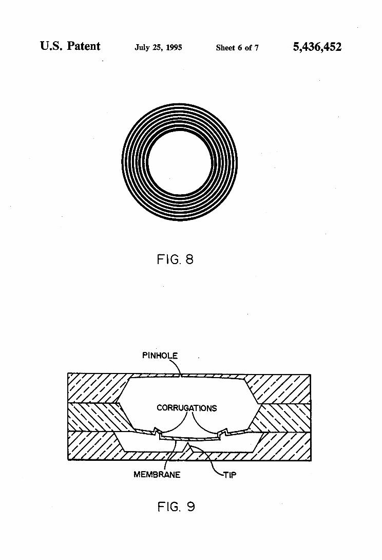
OBJECTS OF THE INVENTION FIG. 8 is a drawing of pattern etching of concentric It is therefore a principal object of the present inven- 40 Circular trenches in a silicon substrate forming corruga-
tion to provide a broadband, uncooled, tunneling infra- tions in the membrane of the invention; red sensor which employs an electrostatically stabilized FIG. 9 is a conceptual drawing of an alternative em- membrane and a feedback circuit to detect infrared bodiment of the invention illustrating the use of mem- radiation. brane corrugations and a membrane pinhole aperture to
It is still an additional object of the present invention to provide a tunneling infrared sensor that is relatively insensitive to environmental temperature variations.
It is still an additional object of the present invention n e present invention comprises an uncooled infra- 5 to provide a tunneling infrared sensor which is config-
ured to eliminate environmental contamination of the tunneling electrodes and acoustic coupling to the sen- sor-
deflection ofa nitride, flat diaphragm membrane. The aforementioned objects and advantages of the
FIG. is a drawing of a
invention;
red Sensor of the present invention;
6;
It is an additional object of the invention to provide 45 improve performance; an uncooled, broadband, tunneling infrared sensor that FIG* lo is a drawing of an =sembled tunneling infra-
a membrane within tunneling distance of a mi- cromachined tip and comprising a feedback circuit to electrostatically retain that distance despite mechanical forces tending to deflect the membrane.
It is still an additional object of the invention to pro- vide a tunneling infrared sensor having micromachined silicon components. INVENTION
red sensor in accordance with the alternative embodi- ment; and
FIG. 11 is a drawing illustrating the assembled sensor 50 of FIG. 10 in a dual in-line electrical package prior to
attachment of a silicon window.
DETAILED DESCRIPTION OF THE
It is still an additional object of the present invention 55 ne present invention utilizes an electron tunneling
ical structure including a deflectable membrane silicon. ~ i ~ ~ ~ ~ ~ ~ b ~ has been used to produce cm- wherein the resonant frequency is greater than 30 KHz. scale components with pm-scale precision. ~ i ~ ~ ~ ~ -
It is still an additional object of the present invention c&g a favorable fabrication tec~ology be- to provide a tunneling infrared sensor employing a cor- 60 cause it allows for -&tion and integration with
to provide a infrared Sensor having a mechan- displacement transducer composed of micro-machined
rugated silicon nitride membrane to permit large deflec- electronics. This device was designed for incorporation tiOnS without req&g complicated Clamping StruC- into an infrared de rector and was optimized to make tures or extremely high deflection voltages to overcome assembly and testing of the IR detector convenient. membrane stiffness. The relative position of the deflection electrodes in
It is still an additional object of the present invention 65 the inventive transducer is controlled though use of to provide a tunneling infrared sensor having litho- electrostatic forces applied between the elements. The graphically prepared, atomically clean, gold tunneling electrostatic forces induce deflection of a gold-coated electrodes. micro-machined silicon nitride membrane. Replace-

5 5,436,452
ment of conventional piezoelectric actuators with an electrostatic actuator is important for the following reasons: First, the electrostatic actuator is insensitive to thermal drifts and immune to the problems of creep associated with piezoelectric actuators. Second, the response of the electrostatic actuator is a function only of the geometry and mechanical properties of the de- vice, whereas the response of piezoelectric actuators is also dependent on the characteristics of the material, which may not be reproducible between devices or over time. Finally, the electrostatic actuator may be miniaturized more easily because the scaling laws are known exactly, and the fabrication is less complex than for the piezoelectric actuator.
Tunneling sensors are fabricated by the following lithographic procedure: Silicon wafers which have al- ready been micromachined to form 30 pm deep recesses with tips are passivated with 1 pm Si02 using a standard steam oxidation process. These wafers are spin-coated with photoresist, and exposed to a lithographic pattern which is used to define the electrode pattern. After development, which removes the exposed photoresist, the wafers are treated in a plasma of 0 2 , which removes organic residue from the open areas in the photoresist pattern, and sharpens the edge profile of the photoresist.
Metal is then deposited on the photoresistcoated wafer. Gold does not adhere well to clean SiOz, so an adhesion layer of another metal is required before the gold is deposited. Typically, chrome is used, because the first chrome layers deposited readily oxidize, and bond well to Si02, while the last layers are metallic, and bond well to the gold. Unfortunately, chrome can mi- grate through the gold layer, eventually forming a non- conductive Cr203 layer on the surface. We have experi- mentally observed the failure of devices due to the appearance of chrome on the surface of the gold tunnel- ing electrodes. After numerous experimenots, we have found that a titanium adhesion layer (150 A), followed by a platinum barrier !ayer (150 A), followed by a gold electrode layer (2000 A) produces atomically clean gold electrodes. The use of a barrier layer has been widely used in industrial applications by others to prevent dif- fusion of the electrode metal down into GaAs sub- strates. We are the first to use such a metal system to prepare atomically clean electrodes for tunneling.
After deposition of the metal layers, the wafer is submerged in a photoresist dissolving solvent (such as acetone) and agitated ultrasonically. The agitation is required for the solvent to soak under the metal which is deposited on photoresist and lift it off.
Finally, the wafers are diced by a standard dicing saw, degreased with TCE, acetone, and methanol, and then treated in plasma of 0 2 for an extended time. The 0 2 plasma removes residual hydrocarbons from the gold electrode surfaces.
As a result of this process, patterned, clean electrodes are produced which are suitable for use in a miniature tunneling transducer.
The electron tunneling displacement transducer de- scribed above was designed to be used with an infrared sensor. The design of the other components of the infra- red sensor was guided by a calculation of its sensitivity. The response and noise of the prototype electron tun- neling infrared de rector are calculated as for a generic thermal detector. It is important to note that this proto- type has not been fully optimized to achieve the best possible sensitivity.
5
10
15
20
25
30
35
40
45
50
55
60
65
6 A cavity of area 0.01 cm2 and thickness 0.015 cm,
filed with air at atmospheric pressure is trapped be- tween a pair of silicon wafers, one of which has been etched through to a 0.5 pm thick silicon oxynitride membrane as shown in FIG. 1. The outer surface of the membrane is coated with - 100 A of gold to serve as an electrode for tunneling as well as an efficient absorber of infrared radiation. The heat capacities of the gas, membrane, and gold films sum to C=7.9x 10⁻⁷ J/K, and the thermal conductances between these elements and the surroundings sum to G= 1.9X 10⁻⁴ W/K. The heat capacity is dominated by the membrane, while the thermal conductance is dominated by conduction through the trapped gas to the window. The mechani- cal properties of the membrane may be calculated, given its dimensions. The coefficient of motion (change in position per unit change in temperature) of the center of the membrane is approximately 1 X 10⁻⁴ cm/K, as- suming that air is an ideal gas at room temperature and pressure. When biased at fvred voltage, the tunneling current has the following dependence on tip-substrate separation:
where Q, is the tunnel b@er height in eV, s is the tip- membrane separation in A, $nd /3 is a conversion factor with a value of 1.025 eV-&A-1. The combined temper- ature coefficient (fractional change in current per unit change in temperature) of trapped gas and tunnel sensor is a=(l/I)(aI/aT)=2.3Xl@/K for Q,=5 eV. This large temperature coefficient is a product of the large thermal expansion of gases at room temperature, and the extreme sensitivity of vacuum tunneling to changes in relative position. For comparison, a for a high per- formance resistance bolometer is approximately equal to 1. The responsivity of the electron tunneling infrared detector is then given by:
The contributions of several kinds of noise must be considered. For each source, an expression for the square off the Noise Equivalent Power, (NEP)2 ap- pears. The NEP is defined as the signal power that would be detected with a unity signal-to-noise ratio in the presence of a given source of noise. The NEP is an important figure of merit for infrared detectors. The expression for the NEP refers to a bandwidth of 1 Hz. Since the noise sources being considered are broadband, reducing the bandwidth of the measurement (increasing the integration time) is expected to improve the sensitiv- ity. An absorber efficiency of 100% is assumed in this expression.
The expression for the NEP of a thermal infrared detector is:
The first term arises due to temperature fluctuations in the trapped gas, the second term is due to shot noise in the tunnel current, and the third term is due to photon noise. In the is expression, kp is Boltzmann's constants, T is the operating temperature, o is the modulation

7 5,436,452
frequency., A is the absorbing area of the detector, and u is the Stefan-Boltzmann constant. Ideally, photon noise would be the largest term in the expression for the NEP.
Noise in amplifiers should not play an important role 5 due to the large transducer sensitivity. Commercial operational ampwiers are readily available that contrib- ute less than the shot noise term to the NEP. A proto- type tunneling transducer was fabricated from mi- cromachined silicon and made operational to investi- 10 gate unexpected noise sources, such as l/f noise. Over the range of frequencies investigated (2 Hz-10 kHz), all sources of transducer noise were smaller than the ex- pected thermal noise from Equation 4.
sider the 50% efficiency of the absorber, the predicted NEP of the prototype is 6 x 10-11 W d H z at chopping frequencies below 10 kHz. At frequencies below 10 kHz, the NEP is dominated by thermal fluctuations. At frequencies above 10 kHz, the contribution from shot 20 noise dominates the other sources of noise and degrades the NEP of the detector. The calculated contributions to the NEP of the prototype are plotted as a function of frequency in FIG. 2.
been fabricated. It is illustrated in FIG. 3. The proto- type infrared sensor was made operational and infrared response was observed with a variety of laboratory blackbody sources. A careful calibration was carried out by chopping between 300" K. and 77" K. blackbo- 30 dies with area 1 cm2 located 10 cm from the sensor. Considering the geometric factors and allowing for atmospheric transmittance from source to sensor, the average modulated signal power at the sensor was 1.6x 10⁻⁷ W. The signal to noise ratio at the chopping 35 frequency of 10 Hz was measured to be 200dHz, so the experimental NEP of the prototype infrared sensor is 8X 1O-loWdHz. Noise in this prototype was domi- nated by the sensitivity of the transducer to mechanical vibration. 40
The measured sensitivity of the tunneling infrared sensor is already competitive with the best commercial pyroelectric sensors and can be readily improved by an order of magnitude through the use of an optimized transducer. 45
The prototype tunneling infrared sensor described above was designed to demonstrate the concept of an infrared sensor based on the tunneling displacement transducer. Since it relied upon the first use of a tunnel- ing device made entirely from micromachined silicon, 50 certain characteristics were selected to allow easy oper- ation, instead of optimized sensitivity. With the success- ful demonstration of this concept, it was appropriate to consider designs that optimize performance.
to environmental sources of noise. For example, an infrared detector should not be especially sensitive to vibration. As is well known, early S m s were extraor- dinarily sensitive to vibration, and required the con- struction of large, complex vibration isolation systems 60 in order to be used. In order to adapt tunneling for use as a transducer for real applications, the sensitivity to vibration, as well as other environmental stimuli, such as temperature and pressure, must be reduced. Since the tunneling infrared sensor is fundamentally a mechanical 65 structure, the sensitivity to vibration is to be eliminated through careful mechanical design. When a mechanical element is subjected to an acceleration at frequencies
If one sums these contributions to the noise, and con- 15
A prototype electron tunneling infrared sensor has 25
It is important for any infrared sensor to be insensitive 55
8 below its resonance, the amplitude of deflection is in- versely proportional to the square of the resonant fre- quency. Therefore, sensitivity to vibration is best re- duced by increasing the resonant frequency of the ele- ments of the transducer.
To meet the operational requirements for sensing applications of a tunneling infrared sensor, we have designed a new series of micromachined actuators. These new actuators are important because they are designed to offer resonant frequencies above 10 ICHZ. The new actuators achieve the higher resonant frequen- cies primarily through reduction in actuator mass by more than 4 orders of magnitude. As a result, the new actuators have smaller range of deflection (<5 pm), which precludes their use for coarse approach between tunneling electrodes. However, with the use of mi- cromachining techniques, it is possible to assemble sen- sors with the electrode spacing already within the range of the fine control, thereby accomplishing the coarse approach during assembly.
A wide-bandwidth actuator used in the present inven- tion simply consists of a flat diaphragm. These dia- phragms are fabricated by coating the front surface of a silicon wafer with low-stress LPCVD silicon nitride. The diaphragms are released by etching square holes through the wafer from the backside with a chemical etchant which does not etch silicon nitride, such as EDP. A drawing of a diaphragm positioned above the tunneling and deflection electrodes is shown in FIG. 5. This device is operated by applying a 150 mV tunneling bias to the tip and groundig the electrode on the mem- brane. A large voltage is applied to the deflection elec- trodes, electrostatically attracting the diaphragm dcwn towards the tip. When the membrane is within 10 A of the tip, a tunnel current of 1 nA appears. The feedback loop compares this current to a reference value and applies an error signal to the deflection electrode, thereby maintaining the position of the diaphragm. If a force is applied to the diaphragm, the feedback loop responds with a balancing force which keeps the dia- phragm position fured. When infrared radiation is ab- sorbed in the sensor, the resulting change in pressure is sensed by the feedback circuit which responds by changing the deflection voltage. The variations in de- flection voltage are proportional to variations in ab- sorbed infrared power.
For the infrared sensor, the dimensions of the dia- phragm are 2 x 2 mm2X0.5 pm. The resonant fre- quency and stiffness are calculated to be 20 kHz and 1 N/m respectively.
With the lowest mechanical resonant frequency of the sensor being above 10 kHz, the gain and bandwidth of the electrical circuit used to control the sensor may be substantially larger than that used in typical STMs or in previous tunneling sensors. Because of this, the feed- back circuitry used may be simplified. FIG. 5 shows a typical feedback circuit that has been used to control tunneling between a micromachined tip and the dia- phragm actuator.
A voltage drop across a 10 MOhm resistor in series with the tip occurs whenever tunneling occurs. A low noise FET input operational amplifier in follower con- figuration is used to lower the source impedance. In this configuration, the output of the first preamplifier never exceeds the range between the bias voltage of 150 mV and ground. We have found this preamplifier configura- tion to be more stable than other possible circuits, such as virtual ground configuration which drives the pream-

9 5,436,452
10 plifier all the way to the supply voltage in the event of c) The tunneling electrodes, which are positioned a tip contact. A simple op-amp circuit is then used to below the gas volume, but exposed to air, are sub- compare the preamplifier output with a reference input ject to contamination. Particularly severe contami- and generate an error signal. This low-voltage, wide- nation problems were observed during tests in bandwidth error signal must then be added to a high- 5 high-humidity conditions. voltage, nmow-bandwidth offset to produce the volt- d) The, sensor is also sensitive to acoustic vibration is age which is applied to the deflection electrodes. The present in the laboratory. high voltage signal may be generated by a power supply In spite of these behavioral ComPliCatio~, e v e s - which is periodically adjusted to keep the error signal merits were carried Out Which confumed very good near zero. A simple high voltage amplifier circuit with 10 sensor performance. However, these behavioral com- very low bandwidth can perform this function as well. plications would be unacceptable in any prototype sen- These transducers were made operational and routine sor being prepared for delivery to a user laboratory.
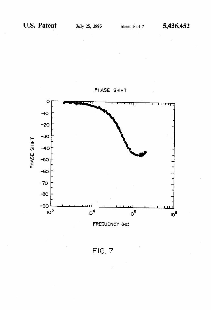
characte-tions were c-ed out. FIG. 6 shows a Several modifications to the design, assembly and measurement of the bandwidth of the transducer. To packaging of these sensors were incorporated in an
a white noise voltage 15 alternate embodiment illustrated in FIGS. 8-11 to en-
These modifications were: a) Use of a corrugated diaphragm to increase flexibil-
out this source is added to the reference input of the feedback able routine operation and delivery to user agencies. loop. The feedback loop responds by generating a cor- responding amplified signal with a white noise distribu- tion at the deflection electrode, which causes fluctua-
tions in the tunneling current. FIG. 6 shows the ratio of the measured fluctuation amplitude to the reference fluctuation amplitude as a function of frequency as re- corded by a standard spectrum analyzer. At all frequen- cies up to 50 kHz, the transducer is able to accurately reproduce the reference current fluctuations. Above 50
Off because Of the band-
ity over a larger deflection range.
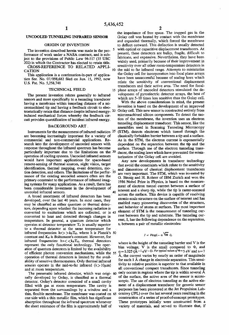
membranes to eliminate dc-sensitivity of the sensor to environmental temperature variations.
c) Use of a sealed chamber with an infrared window to eliminate environmental contamination of the tunneling electrodes and acoustic coupling to the sensor.
tions in the position ofthe diaphragm, as well as fluctua- 2o b) Use of a 0*5 pm diameter pinhole in one of the
25
These modifications have resulted in a set of this response begins to ing infrared sensors which are appropriate for routine
between the measured and requested current* This 30 be described in more detail with reference to FIGS. phase shift is less than (5 degrees for frequencies below 10 m, and increases to 30 degrees at 50 mz. At fie- com-
the noise source and the transducer begins to contribute rapidy for deflections larger than the thickness of the to the measurement, as evidenced by the variation in the 35 diaphragm. the case of the tunneling infrared sensor, phase shift at those frequencies. the diaphragm thickness is 0.5 pm, and the desired
Recent mdications to the design of the tunneling range of deflection is 3-5 pm. The introduction of cor- infrared sensor simplify fabrication and operation ofthe rugations into the diaphragm will delay the onset of the device. These modifications include incorporation of stiffness increase. Accordingly, a ,-omgated silicon corrugated diaphragms for increased fleibilitY and 40 nitride diaphragm may be fabricated in the following lower voltage operation, submicron pinholes for long- manner: term stability, and packaging techniques Which allow a) Prepare a high-resolution photo mask which con- use of hybrid-integrated circuitry and greatly simplified sists of sets of concentric circular openings of even mounting and testing procedures. With these modifica- contrast and 20 pm pitch. (see FIG. 8) tions, the performance has been enhanced to exceed 45 b) Print this pattern on a photoresist-covered bare that of all other commercially available uncooled infra- silicon wafer (of dimensions 3” in diameterX200 red sensors. Operation of these sensors has been simpli- pm thickness in a standard configuration). fied to the extent that they have been shipped to non- c) Etch the pattern 1 pm into the surface of the wafer expert users for routine testing and evaluation at their using a reactive ion etching apparatus and sulfur laboratories. 50 hexafluoride as the etchant.
The assembly and operation of the sensor of FIG. 4 d) Grow a thick oxide on all surfaces of the wafer and was complicated by several non-ideal characteristics: then etch the oxide in hydrofluoric acid. This step
a) The silicon nitride membranes fabricated for the smoothes the surface of the wafer, and rounds the tunneliig sensors suffered from stiffness which circular trenches previously etched in the wafer. increased rapidly with deflection. For the required 55 e) Deposit 0.5 pm oflow-stress silicon nitride using a deflections of 3-5 pm, the stiffness increased from low-pressure chemical vapor deposition system. 1.5 N/m to more than 100 N/m. As a result, com- This nitride conformally coats all surfaces of the plicated clamping structures were required to re- wafer, including the rounded corrugations. duce the tip-membrane separation, and extremely 4 Etch square openings in the silicon nitride on the high deflection voltages (>W V) were required. 60 side of the wafer opposite to the previous etching
b) The total pressure of gas trapped within the cell is of the circular trenches. strongly dependent on the temperature of the envi- g) Etch the entire wafer in a silicon etching solution ronment surrounding the sensor. As a result, the such as potassium hydroxide until the membranes deflection voltage required to operate the sensor are released. was subject to rapid drifts during normal operation. 65 The corrugated diaphragms fabricated in this way During typical operation, it was neceSSary to phys- were immediately incorporated into a set of tunneling ically adjust the mounting clamps to compensate infrared sensors with the following results: The me- for changes in room temperature every half hour. chanical clamping structure used to help overcome the
width Of the PrmPlifier- FIG* the phase shift testing by non+xperts at user laboratories and will now
8-11. It is in the
quenci@ above loo IrHz, capacitive between munity that the stiffness of flat diaphragms can increase
.

5,436,452 11
initial tip-membrane separation could be greatly simpli- fied; and the operating voltages of the tunneling infra- red sensors were reduced to below 150 V for all sensors and as low as 40 V for several sensors, allowing shplifi- cation of the feedback circuitry.
The variations in operating voltage with room tem- perature can be eliminated by introduction of a small leak in the gas cavity, allowing the pressure to equili- brate. It is important that this leak be very small, so as to preserve the detection of the raidation-induced pres- sure fluctuations at>5 Hz frequencies. Given the di- mensions of the cavity, and the thickness of the dia- phragm, molecular dynamics calculations indicate that a pinhole diameter of 0.5 pm is required to achieve a 1 second time constant.
Since optical lithographic techniques available to the inventors cannot be utilized to reliably fabricate fea- tures of such size, are e-beam lithography system was again utilized. Optical lithographic techniques may also be used if sufficient resolution is available. The proce- dure for the fabrication of the pinholes is:
a) Coat a 3" x 200 pm wafer with 0.5 pm of low-stress silicon nitride on surfaces.
b) Evaporate a 300 A thick layer of aluminum on one side of the wafer.
c) Coat the aluminum-side of the wafer with e-beam photoresist, and expose a series of 0.5 pm-diameter openings in the photoresist.
d) Develop the resist, producing the 0.5 pm diameter openings.
e) Etch ,the wafer in AZ 400K developer solution or any weak basic solution to remove the exposed aluminum under the e-beam written pinholes.
f ) Etch the entire wafer in a reactive ion etching apparatus with carbon tetrafluroide gas to remove the silicon nitride under the openings in the alumi- num.
g) Etch square openings in the silicon nitride on the opposite side of the wafer.
h) Etch the entire wafer in potassium hydroxide solu- tion until the diaphragms have been relased. These diaphragms will have 0.5 pm openings already in place.
Once fabricated, several of these perforated dia- phragms were incorporated into tunneliig infrared sen- sors. A drawing showing the location of the corrugtions and perforation in the sensor is shown in FIG. 9. Mea- surements with these sensors confirmed that time-con- stants between 0.2 and 5 seconds were achieved. Tun- neling infrared sensors based on these perforated mem- branes exhibited the following behavior: The operating voltage did not drift with the environmental tempera- ture; and the sensor clamping structure could be elimi- nated entirely in favor of a completely bonded structure within a standard integrated circuit carrier. This pack- aging approach is shown in FIG. 10.
These sensors were tested in several environments and shown to be sensitive to environmental contamina- tion of the electrodes as well as acoustic coupling to the room. These problems were both solved by sealing the sensor in a small volume of air within the integrated circuit test package with a silicon window. The silicon window is used because it is transparent in the infrared, mechanically stiff enought to eliminate acoustic cou- pling, inexpensive, and readily available. Other infrared windows may also be used. The final design of these tunneling infrared sensors is shown in FIG. 11.
5
10
15
20
25
30
35
40
45
50
55
60
65
12 Sensors incorporating these features of the alternative
embodiment have been operated routinely over ex- tended periods of time by users without expertise in the detailed operation of tunneling infrared sensors.
Having thus described an exemplary embodiment of the invention, what is claimed is: 1. An infrared sensor comprising: an enclosed chamber; a gas in said chamber; a metal coated corrugated silicon nitride membrane
forming a deflectable wall of said enclosed cham- ber;
a metal coated silicon tip within tunneling distance of said membrane for establishing a tunneling current therebetween depending upon said distance;
at least one electrode in spaced, opposing proximity to said membrane for electrostatically controlling the deflection of said membrane; and
a feedback circuit connected to said electrode for generating a servo feedback voltage for maintain- ing the deflection of said membrane irrespective of the level of infrared radiation incident upon said chamber, the variations in said servo feedback volt- age being proportional to the variations in the level of infrared radiation incident upon said chamber.
2. The infrared sensor recited in claim 1 wherein said membrane is coated with gold.
3. The infrared sensor recited in claim 1 wherein said tip is coated with gold. 4. The infrared sensor recited in claim 1 wherein said
membrane is coated with a layer of adhesion material, a layer of barrier material and a layer of metal.
5. The infrared sensor recited in claim 4 wherein said adhesion material is titanium. 6. The infrared sensor recited in claim 4 wherein said
barrier material is platinum. 7. The infrared sensor recited in claim 4 wherein said
metal is gold. 8. The infrared sensor recited in claim 1 wherein said
tip is coated with a layer of adhesion material, a layer of barrier material and a layer of metal.
9. The infrared sensor recited in claim 8 wherein said adhesion material is titanium. 10. The infrared sensor recited in claim 8 wherein
said barrier material is platinum. 11. The infrared sensor recited in claim 8 wherein
said metal is gold. 12. The infrared sensor recited in claim 1 wherein
said gas is air and wherein said chamber comprises an aperture of selected sue, said aperture permitting lim- ited air movement into and out of said chamber to com- pensate for environmental temperature variations. 13. The infrared sensor recited in claim 1 wherein
said gas is xenon and wherein said chamber comprises an aperture of selected size, said aperture permitting limited xenon movement into and out of said chamber to compensate for environmental temperature varia- tions. 14. In a tunneling infrared sensor of the type having a
deflectable membrane forming a wall of an enclosed gas-filed chamber and an electrode tip for establishing a tunneling current dependent upon the deflection of said membrane in response to incident infrared radia- tion; the improvement comprising:
corrugation in said membrane; at least one deflection electrode positioned in spaced
relation to said membrane for electrostatically con- trolling the deflection of said membrane; and

13 5,436,452
14 a feedback circuit connected between said tip and
said electrode and responsive to said tunneling current for maintaining the deflection of said mem- brane within a selected range irrespective of the level of incident infrared radiation,
15. The improvement recited in claim 14 wherein said
average of the operational amplifier output voltage and the offset voltage are applied to the deflection voltage.
18. The improvement recited in claim 14 wherein said 5 membrane has a mechanical resonance frequency which
is at least 10 kHz. feedback circuit produces a voltage at said deflection electrode, the magnitude of variations in said voltage beiig proportional to the magnitude of variations in
16. The improvement recited in claim 15 wherein said
17. The improvement recited in claim 15 wherein said
a resistor network to generate bias and reference 15
a load resistor in series between said tip and ground; an operational amplifier whose inputs are connected
to said tunneling tip and to a reference voltage and whose output is connected through a voltage di- 20 vider to the deflection electrode and a voltage offset, respectively configured so that the weighted
infrared radiation incident upon the sensor. 10
feedback circuit has a bandwidth of at least 50 kHz.
feedback circuit comprises:
voltages;
19. An infrared sensor comprising: a tunneling transducer configured for generating a
tunneling current dependent upon the level of inci- dent infrared radiation; said tunneling transducer having a tunneling tip and a deflection membrane;
electrostatically controlled deflection means for re- taining the deflection of said membrane substan- tially constant irrespective of said level of said infrared radiation; and
a fixed membrane in spaced relation to said deflection membrane and forming a gas-filled chamber there- between;
said fixed membrane having an aperture of selected sue for reducing the sensitivity of said sensor to environmental temperature variation. * * * * *
25
30
35
40
45
50
55
60
65