
UNIT V MEMORY AND I/O SYSTEMS -...
54
Course Material (Lecture Notes) CS6303 – COMPUTER ARCHITECTURE UNIT-V Page 1 UNIT V MEMORY AND I/O SYSTEMS From the CPU's perspective, an I/O device appears as a set of special-purpose registers, of three general types: x Status registers provide status information to the CPU about the I/O device. These registers are often read-only, i.e. the CPU can only read their bits, and cannot change them. x Configuration/control registers are used by the CPU to configure and control the device. Bits in these configuration registers may be write-only, so the CPU can alter them, but not read them back. Most bits in control registers can be both read and written. x Data registers are used to read data from or send data to the I/O device. In some instances, a given register may fit more than one of the above categories, e.g. some bits are used for configuration while other bits in the same register provide status information. The logic circuit that contains these registers is called the device controller, and the software that communicates with the controller is called a device driver. +-------------------+ +-----------+ | Device controller | | | +-------+ | |<--------->| Device | | |---------->| Control register | | | | CPU |<----------| Status register | | | | |<--------->| Data register | | | +-------+ | | | | +-------------------+ +-----------+ Simple devices such as keyboards and mice may be represented by only a few registers, while more complex ones such as disk drives and graphics adapters may have dozens. Each of the I/O registers, like memory, must have an address so that the CPU can read or write specific registers. Some CPUs have a separate address space for I/O devices. This requires separate instructions to perform I/O operations. Other architectures, like the MIPS, use memory-mapped I/O. When using memory-mapped I/O, the same address space is shared by memory and I/O devices. Some addresses represent memory cells, while others represent registers in I/O devices. No separate I/O instructions are needed in a CPU that uses memory-mapped I/O. Instead, we can perform I/O operations using any instruction that can reference memory. +---------------+ www.studentsfocus.com www.studentsfocus.com
Transcript of UNIT V MEMORY AND I/O SYSTEMS -...

Course Material (Lecture Notes)
CS6303 – COMPUTER ARCHITECTURE UNIT-V Page 1
UNIT V MEMORY AND I/O SYSTEMS
From the CPU's perspective, an I/O device appears as a set of special-purpose registers, of three general types:
x Status registers provide status information to the CPU about the I/O device. These registers are often read-only, i.e. the CPU can only read their bits, and cannot change them.
x Configuration/control registers are used by the CPU to configure and control the device. Bits in these configuration registers may be write-only, so the CPU can alter them, but not read them back. Most bits in control registers can be both read and written.
x Data registers are used to read data from or send data to the I/O device.
In some instances, a given register may fit more than one of the above categories, e.g. some bits are used for configuration while other bits in the same register provide status information.
The logic circuit that contains these registers is called the device controller, and the software that communicates with the controller is called a device driver.
+-------------------+ +-----------+ | Device controller | | | +-------+ | |<--------->| Device | | |---------->| Control register | | | | CPU |<----------| Status register | | | | |<--------->| Data register | | | +-------+ | | | | +-------------------+ +-----------+
Simple devices such as keyboards and mice may be represented by only a few registers, while more complex ones such as disk drives and graphics adapters may have dozens.
Each of the I/O registers, like memory, must have an address so that the CPU can read or write specific registers.
Some CPUs have a separate address space for I/O devices. This requires separate instructions to perform I/O operations.
Other architectures, like the MIPS, use memory-mapped I/O. When using memory-mapped I/O, the same address space is shared by memory and I/O devices. Some addresses represent memory cells, while others represent registers in I/O devices. No separate I/O instructions are needed in a CPU that uses memory-mapped I/O. Instead, we can perform I/O operations using any instruction that can reference memory.
+---------------+
www.studentsfocus.com
www.studentsfocus.com

Course Material (Lecture Notes)
CS6303 – COMPUTER ARCHITECTURE UNIT-V Page 2
| Address space | | +-------+ | | | ROM | | | +-------+ | +-------+address| | | | | |------>| | RAM | | | CPU | | | | | | |<----->| +-------+ | +-------+ data | | | | | | I/O | | | +-------+ | +---------------+
On the MIPS, we would access ROM, RAM, and I/O devices using load and store instructions. Which type of device we access depends only on the address used!
lw $t0, 0x00000004 # Read ROM sw $t0, 0x00000004 # Write ROM (bus error!) lbu $t0, 0x0000ffc1 # Read RAM sb $t0, 0x0000ffc1 # Write RAM lbu $t0, 0xffff0000 # Read an I/O device sb $t0, 0xffff0004 # Write to an I/O device
The 32-bit MIPS architecture has a 32-bit address, and hence an address space of 4 gigabytes. Addresses 0x00000000 through 0xfffeffff are used for memory, and addresses 0xffff0000 - 0xffffffff (the last 64 kilobytes) are reserved for I/O device registers. This is a very small fraction of the total address space, and yet far more space than is needed for I/O devices on any one computer.
Each register within an I/O controller must be assigned a unique address within the address space. This address may be fixed for certain devices, and auto-assigned for others. (PC plug-and-play devices have auto-assigned I/O addresses, which are determined during boot-up.)
www.studentsfocus.com
www.studentsfocus.com

Course Material (Lecture Notes)
CS6303 – COMPUTER ARCHITECTURE UNIT-V Page 3
MEMORY HIERARCHY
www.studentsfocus.com
www.studentsfocus.com
Sri Vidya College of Engineering & Technology, Virudhunagar Course Material (Lecture Notes)
CS6303 – COMPUTER ARCHITECTURE UNIT-V Page 4
www.studentsfocus.com

Sri Vidya College of Engineering & Technology, Virudhunagar Course Material (Lecture Notes)
CS6303 – COMPUTER ARCHITECTURE UNIT-V Page 5
www.studentsfocus.com

Sri Vidya College of Engineering & Technology, Virudhunagar Course Material (Lecture Notes)
CS6303 – COMPUTER ARCHITECTURE UNIT-V Page 6
www.studentsfocus.com

Sri Vidya College of Engineering & Technology, Virudhunagar Course Material (Lecture Notes)
CS6303 – COMPUTER ARCHITECTURE UNIT-V Page 7
www.studentsfocus.com

Sri Vidya College of Engineering & Technology, Virudhunagar Course Material (Lecture Notes)
CS6303 – COMPUTER ARCHITECTURE UNIT-V Page 8
MEMORY TECHNOLOGIES
Much of the success of computer technology stems from the tremendous progress in storage technology. Early computers had a few kilobytes of random-access memory. The earliest IBM PCs didn’t even have a hard disk.
That changed with the introduction of the IBM PC-XT in 1982, with its 10-megabyte disk. By the year 2010, typical machines had 150,000 times as much disk storage, and the amount of storage was increasing by a factor of 2 every couple of years. Random-Access Memory Random-access memory (RAM) comes in two varieties—static and dynamic. Static RAM (SRAM) is faster and significantly more expensive than Dynamic RAM (DRAM). SRAM is used for cache memories, both on and off the CPU chip. DRAM is used for the main memory plus the frame buffer of a graphics system. Typically, a desktop system will have no more than a few megabytes of SRAM, but hundreds or thousands of megabytes of DRAM. Static RAM SRAMstores each bit in a bistable memory cell. Each cell is implemented with a six-transistor circuit. This circuit has the property that it can stay indefinitely in either of two different voltage configurations, or states. Any other state will be unstable—starting from there, the circuit will quickly move toward one of the stable
Dynamic RAM
DRAM stores each bit as charge on a capacitor. This capacitor is very small—typically around 30 femtofarads,that is, 30 × 10−15 farads. Recall, however, that a farad is a very large unit of measure. DRAM storage can be made very dense—each cell consists of a capacitor and a single access-transistor. Unlike SRAM, however, a DRAM memory cell is very sensitive to any disturbance. When the capacitor voltage is disturbed, it will never recover. Exposure to light rays will cause the capacitor voltages to change. In fact, the sensors in digital cameras and camcorders are essentially arrays of DRAM cells.
www.studentsfocus.com

Sri Vidya College of Engineering & Technology, Virudhunagar Course Material (Lecture Notes)
CS6303 – COMPUTER ARCHITECTURE UNIT-V Page 9
Conventional DRAMs The cells (bits) in a DRAM chip are partitioned into d supercells, each consisting of w
DRAM cells. A d × w DRAM stores a total of dw bits of information. The supercells are organized as a rectangular array with r rows and c columns, where rc = d. Each supercell has an address of the form (i, j), where i denotes the row, and j denotes the column. For example, Figure 6.3 shows the organization of a 16 × 8 DRAM chip with d = 16 supercells, w = 8 534 bits per supercell, r = 4 rows, and c = 4 columns. The shaded box denotes the supercell at address (2, 1). Information flows in and out of the chip via external connectors called pins. Each pin carries a 1-bit signal. Figure shows two of these sets of pins: eight data pins that can transfer 1 byte in or out of the chip, and two addr pins that carry two-bit row and column supercell addresses. Other pins that carry control information are not shown.
Fig: Conventionall DRAM
One reason circuit designers organize DRAMs as two-dimensional arrays instead of linear arrays is to reduce the number of address pins on the chip. For example, if our example 128-bit DRAM were organized as a linear array of 16 supercells with addresses 0 to 15, then the chip would need four address pins instead of two. The disadvantage of the two-dimensional array organization is that addresses must be sent in two distinct steps, which increases the access time.
www.studentsfocus.com

Sri Vidya College of Engineering & Technology, Virudhunagar Course Material (Lecture Notes)
CS6303 – COMPUTER ARCHITECTURE UNIT-V Page 10
Enhanced DRAMs There are many kinds of DRAM memories, and new kinds appear on the market with regularity as manufacturers attempt to keep up with rapidly increasing processor speeds. Each is based on the conventional DRAM cell, with optimizations that improve the speed with which the basic DRAM cells can be accessed. Accessing Main Memory
Data flows back and forth between the processor and the DRAM main memory over shared electrical conduits called buses. Each transfer of data between the CPU and memory is accomplished with a series of steps called a bus transaction. A read transaction transfers data from the main memory to the CPU. A write transaction transfers data from the CPU to the main memory.
A bus is a collection of parallel wires that carry address, data, and control signals. Depending on the particular bus design, data and address signals can share the same set of wires, or they can use different sets. Also, more than two devices can share the same bus. The control wires carry signals that synchronize the transaction and identify what kind of transaction is currently being performed.
Figure : Example bus structure that connects the CPU and main memory.
www.studentsfocus.com

Sri Vidya College of Engineering & Technology, Virudhunagar Course Material (Lecture Notes)
CS6303 – COMPUTER ARCHITECTURE UNIT-V Page 11
Disk Storage Disks are workhorse storage devices that hold enormous amounts of data, on the order of
hundreds to thousands of gigabytes, as opposed to the hundreds or thousands of megabytes in a RAM-based memory. However, it takes on the order of milliseconds to read information from a disk, a hundred thousand times longer than from DRAM and a million times longer than from SRAM.
Figure: Memory read transaction for a load operation
CACHE BASICS – MEASURING AND IMPROVING CACHE PERFORMANCE
One focuses on reducing the miss rate by reducing the probability that two different memory blocks will contend for the same cache location. The second technique reduces the miss penalty by adding an additional level to the hierarchy. This technique, called multilevel caching, first appeared in high-end computers selling for more than $100,000 in 1990; since then it has become common on desktop computers selling for less than $500! CPU time can be divided into the clock cycles that the CPU spends executing the program and the clock cycles that the CPU spends waiting for the memory
www.studentsfocus.com

Sri Vidya College of Engineering & Technology, Virudhunagar Course Material (Lecture Notes)
CS6303 – COMPUTER ARCHITECTURE UNIT-V Page 12
system. Normally, we assume that the costs of cache accesses that are hits are part of the normal CPU execution cycles. Thus,
CPU time = (CPU execution clock cycles T Memory-stall clock cycles) The memory-stall clock cycles come primarily from cache misses, and we make
that assumption here. We also restrict the discussion to a simplified model of the memory system. In real processors, the stalls generated by reads and writes can be quite complex, and accurate performance prediction usually requires very detailed simulations of the processor and memory system.
Reads Read-stall cycles =Pr ogram x Read miss rate x Read miss penalty Writes are more complicated. For a write-through scheme, we have two sources of stalls: write misses, which usually require that we fetch the block before continuing the write (see the Elaboration on page 467 for more details on dealing with writes), and write buffer stalls, which occur when the write buffer is full when a write occurs.
Calculating Cache Performance:
Assume the miss rate of an instruction cache is 2% and the miss rate of the data
cache is 4%. If a processor has a CPI of 2 without any memory stalls and the miss penalty is 100 cycles for all misses, determine how much faster a processor would run with a perfect cache that never missed. Assume the frequency of all loads and stores is 36%.
Reducing Cache Misses by Move Flexibfle Placement of Blocks
So far, when we place a block in the cache, we have used a simple placement
scheme: A block can go in exactly one place in the cache. As mentioned earlier, it is called direct mapped because there is a direct mapping from any block address in memory to a single location in the upper level of the hierarchy. However, there is actually a whole range of schemes for placing blocks. Direct mapped, where a block can be placed in exactly one location, is at one extreme. At the other extreme is a scheme where a block can be placed in any location in the cache. Such a scheme is called fully associative, because a block in memory may be associated with any entry in the cache. To find a given block in a fully associative cache, all the entries in the cache must be searched because a block can be placed in any one. To make the search practical, it is done in parallel with a comparator associated with each cache entry. These comparators significantly increase the hardware cost, effectively making fully associative placement practical only forcaches with small numbers of blocks.
www.studentsfocus.com

Sri Vidya College of Engineering & Technology, Virudhunagar Course Material (Lecture Notes)
CS6303 – COMPUTER ARCHITECTURE UNIT-V Page 13
Choosing Which Block to Replace : When a miss occurs in a direct-mapped cache, the requested block can go in exactly one position, and the block occupying that position must be replaced. In an associative cache, we have a choice of where to place the requested block, and hence a choice of which block to replace. In a fully associative cache, all blocks are candidates for replacement. In a set-associative cache, we must choose among the blocks in the selected set. The most commonly used scheme is least recently used (LRU), which we used in the previous example. In an LRU scheme, the block replaced is the one that has been unused for the longest time. The set associative example on page 482 uses LRU, which is why we replaced Memory(O) instead of Memory(6). LRU replacement is implemented by keeping track of when each element in a set was used relative to the other elements in the set. For a two-way set-associative cache, tracking when the two elements were used can be implemented by keeping a single bit in each set and setting the bit to indicate an element whenever that element is referenced. As associativity increases, implementing LRU gets harder; in Section 5.5, we will see an alternative scheme for replacement.
www.studentsfocus.com

Sri Vidya College of Engineering & Technology, Virudhunagar Course Material (Lecture Notes)
CS6303 – COMPUTER ARCHITECTURE UNIT-V Page 14
www.studentsfocus.com

Sri Vidya College of Engineering & Technology, Virudhunagar Course Material (Lecture Notes)
CS6303 – COMPUTER ARCHITECTURE UNIT-V Page 15
www.studentsfocus.com

Sri Vidya College of Engineering & Technology, Virudhunagar Course Material (Lecture Notes)
CS6303 – COMPUTER ARCHITECTURE UNIT-V Page 16
www.studentsfocus.com

Sri Vidya College of Engineering & Technology, Virudhunagar Course Material (Lecture Notes)
CS6303 – COMPUTER ARCHITECTURE UNIT-V Page 17
www.studentsfocus.com
Sri Vidya College of Engineering & Technology, Virudhunagar Course Material (Lecture Notes)
CS6303 – COMPUTER ARCHITECTURE UNIT-V Page 18
www.studentsfocus.com

Sri Vidya College of Engineering & Technology, Virudhunagar Course Material (Lecture Notes)
CS6303 – COMPUTER ARCHITECTURE UNIT-V Page 19
www.studentsfocus.com

Sri Vidya College of Engineering & Technology, Virudhunagar Course Material (Lecture Notes)
CS6303 – COMPUTER ARCHITECTURE UNIT-V Page 20
www.studentsfocus.com

Sri Vidya College of Engineering & Technology, Virudhunagar Course Material (Lecture Notes)
CS6303 – COMPUTER ARCHITECTURE UNIT-V Page 21
www.studentsfocus.com

Sri Vidya College of Engineering & Technology, Virudhunagar Course Material (Lecture Notes)
CS6303 – COMPUTER ARCHITECTURE UNIT-V Page 22
www.studentsfocus.com

Sri Vidya College of Engineering & Technology, Virudhunagar Course Material (Lecture Notes)
CS6303 – COMPUTER ARCHITECTURE UNIT-V Page 23
www.studentsfocus.com

Sri Vidya College of Engineering & Technology, Virudhunagar Course Material (Lecture Notes)
CS6303 – COMPUTER ARCHITECTURE UNIT-V Page 24
www.studentsfocus.com

Sri Vidya College of Engineering & Technology, Virudhunagar Course Material (Lecture Notes)
CS6303 – COMPUTER ARCHITECTURE UNIT-V Page 25
www.studentsfocus.com

Sri Vidya College of Engineering & Technology, Virudhunagar Course Material (Lecture Notes)
CS6303 – COMPUTER ARCHITECTURE UNIT-V Page 26
www.studentsfocus.com

Sri Vidya College of Engineering & Technology, Virudhunagar Course Material (Lecture Notes)
CS6303 – COMPUTER ARCHITECTURE UNIT-V Page 27
VIRTUAL MEMORY
Similarly, the main memory can act as a "cache" for the secondary storage, usually implemented with magnetic disks. This technique is called virtual memory. Historically, there were two major motivations for virtual memory: to allow efficient and safe sharing of memory among multiple programs, and to remove the programming burdens of a small, limited amount of main memory. Four decades after its invention, it's the former reason that reigns today.
Consider a collection of programs running all at once on a computer. Of course, to allow multiple programs to share the same memory, we must be able to protect the programs from each other, ensuring that a program can only read and write the portions of main memory that have been assigned to it. Main memory need contain only the active portions of the many programs, just as a cache contains only the active portion of one program. Thus, the principle of locality enables virtual memory as well as caches, and virtual memory allows us to efficiently share the processor as well as the main memory. The second motivation for virtual memory is to allow a single user program to exceed the size of primary memory. Formerly, if a program became too large for memory, it was up to the programmer to make it fit. Programmers divided programs into pieces and then identified the pieces that were mutually exclusive. These overlays were loaded or unloaded under user program control during execution, with the programmer ensuring that the program never tried to access an overlay that was not loaded and that the overlays loaded never exceeded the total size of the memory. Overlays were traditionally organized as modules, each containing both code and data.
In virtual memory, the address is broken into a virtual page number and a page offset. Figure 5.20 shows the translation of the virtual page number to a physical page number. The physical page number constitutes the upper portion of the physical address, while the page offset, which is not changed, constitutes the lower portion. The number of bits in the page offset field determines
www.studentsfocus.com
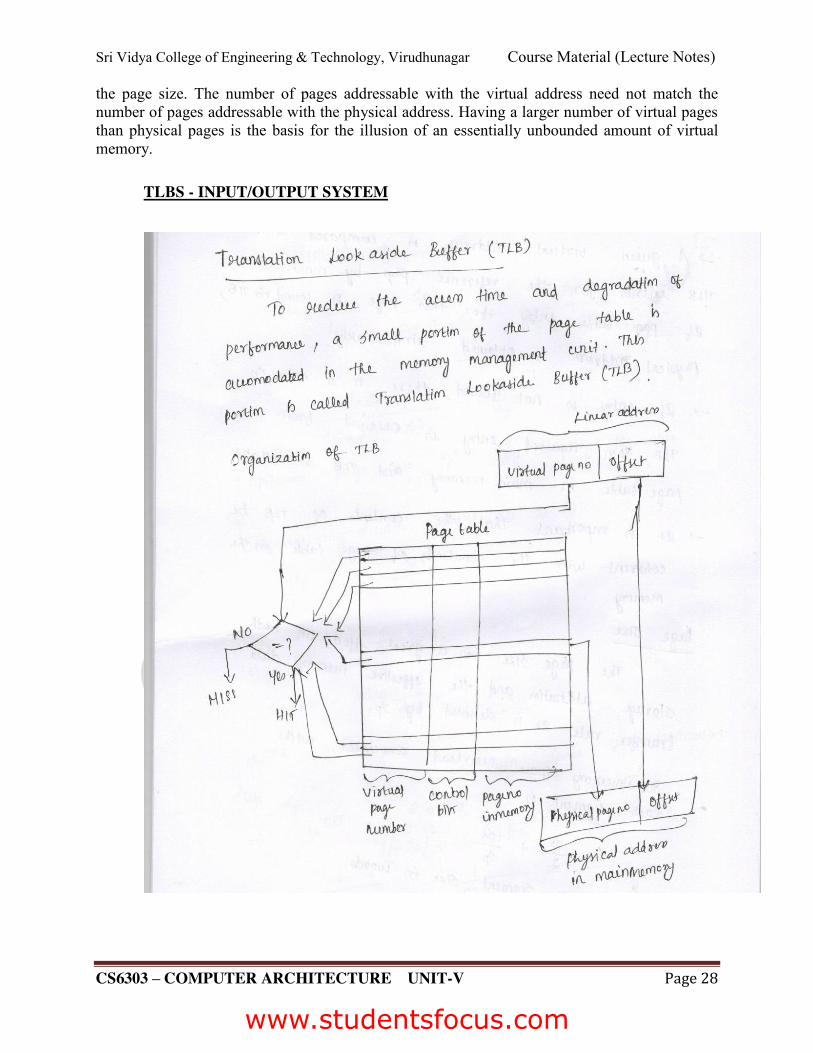
Sri Vidya College of Engineering & Technology, Virudhunagar Course Material (Lecture Notes)
CS6303 – COMPUTER ARCHITECTURE UNIT-V Page 28
the page size. The number of pages addressable with the virtual address need not match the number of pages addressable with the physical address. Having a larger number of virtual pages than physical pages is the basis for the illusion of an essentially unbounded amount of virtual memory.
TLBS - INPUT/OUTPUT SYSTEM
www.studentsfocus.com

Sri Vidya College of Engineering & Technology, Virudhunagar Course Material (Lecture Notes)
CS6303 – COMPUTER ARCHITECTURE UNIT-V Page 29
www.studentsfocus.com

Sri Vidya College of Engineering & Technology, Virudhunagar Course Material (Lecture Notes)
CS6303 – COMPUTER ARCHITECTURE UNIT-V Page 30
www.studentsfocus.com

Sri Vidya College of Engineering & Technology, Virudhunagar Course Material (Lecture Notes)
CS6303 – COMPUTER ARCHITECTURE UNIT-V Page 31
www.studentsfocus.com

Sri Vidya College of Engineering & Technology, Virudhunagar Course Material (Lecture Notes)
CS6303 – COMPUTER ARCHITECTURE UNIT-V Page 32
www.studentsfocus.com

Sri Vidya College of Engineering & Technology, Virudhunagar Course Material (Lecture Notes)
CS6303 – COMPUTER ARCHITECTURE UNIT-V Page 33
www.studentsfocus.com

Sri Vidya College of Engineering & Technology, Virudhunagar Course Material (Lecture Notes)
CS6303 – COMPUTER ARCHITECTURE UNIT-V Page 34
www.studentsfocus.com

Sri Vidya College of Engineering & Technology, Virudhunagar Course Material (Lecture Notes)
CS6303 – COMPUTER ARCHITECTURE UNIT-V Page 35
www.studentsfocus.com

Sri Vidya College of Engineering & Technology, Virudhunagar Course Material (Lecture Notes)
CS6303 – COMPUTER ARCHITECTURE UNIT-V Page 36
www.studentsfocus.com

Sri Vidya College of Engineering & Technology, Virudhunagar Course Material (Lecture Notes)
CS6303 – COMPUTER ARCHITECTURE UNIT-V Page 37
www.studentsfocus.com

Sri Vidya College of Engineering & Technology, Virudhunagar Course Material (Lecture Notes)
CS6303 – COMPUTER ARCHITECTURE UNIT-V Page 38
Input/Output The computer system’s I/O architecture is its interface to the outside world. This architecture is designed to provide a systematic means of controlling interaction with the outside world and to provide the operating system with the information it needs to manage I/O activity effectively. There are three principal I/O techniques: programmed I/O, in which I/O occurs under he direct and continuous control of the program requesting the I/O operation; interrupt-driven I/O, in which a program issues an I/O command and then continues to execute, until it is interrupted by the I/O hardware to signal the end of the I/O operations; and direct memory access (DMA), in which a specialized I/O processor takes over control of an I/O operation to move a large block of data. Two important examples of external I/O interfaces are FireWire and Infiniband. Peripherals and the System Bus
There are a wide variety of peripherals each with varying methods of operation Impractical to for the processor to accommodate all Data transfer rates are often slower than the processor and/or memory Impractical to use the high-speed system bus to communicate directly Data transfer rates may be faster than that of the processor and/or memoryThis mismatch
may lead to inefficiencies if improperly managed Peripheral often use different data formats and word lengths Purpose of I/O Modules Interface to the processor and memory via the system bus or control switch Interface to one or more peripheral devices
Purpose of I/O Modules • Interface to the processor and memory via the system bus or control switch • Interface to one or more peripheral devices
www.studentsfocus.com

Sri Vidya College of Engineering & Technology, Virudhunagar Course Material (Lecture Notes)
CS6303 – COMPUTER ARCHITECTURE UNIT-V Page 39
External Devices: External device categories • Human readable: communicate with the computer user – CRT • Machine readable: communicate with equipment – disk drive or tape drive • Communication: communicate with remote devices – may be human readable or machine readable
The External Device – I/O Module • Control signals: determine the function that will be performed • Data: set of bits to be sent of received • Status signals: indicate the state of the device • Control logic: controls the device’s operations • Transducer: converts data from electrical to other forms of energy • Buffer: temporarily holds data being transferred Keyboard/Monitor • Most common means of computer/user interaction • Keyboard provides input that is transmitted to the computer • Monitor displays data provided by the computer • The character is the basic unit of exchange • Each character is associated with a 7 or 8 bit code Disk Drive • Contains electronics for exchanging data, control, and status signals with an I/O module • Contains electronics for controlling the disk read/write mechanism • Fixed-head disk – transducer converts between magnetic patterns on the disk surface and bits in the buffer • Moving-head disk – must move the disk arm rapidly across the surface I/O Modules Module Function • Control and timing • Processor communication
www.studentsfocus.com
Sri Vidya College of Engineering & Technology, Virudhunagar Course Material (Lecture Notes)
CS6303 – COMPUTER ARCHITECTURE UNIT-V Page 40
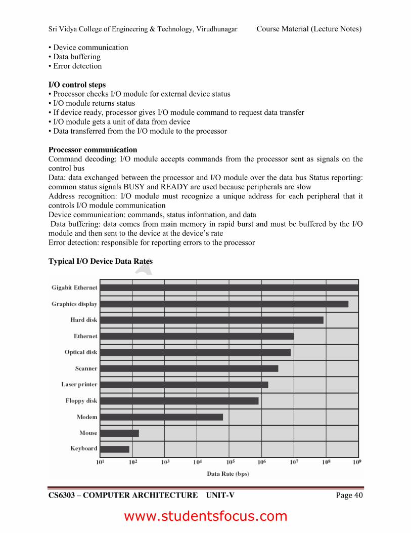
• Device communication • Data buffering • Error detection I/O control steps • Processor checks I/O module for external device status • I/O module returns status • If device ready, processor gives I/O module command to request data transfer • I/O module gets a unit of data from device • Data transferred from the I/O module to the processor Processor communication Command decoding: I/O module accepts commands from the processor sent as signals on the control bus Data: data exchanged between the processor and I/O module over the data bus Status reporting: common status signals BUSY and READY are used because peripherals are slow Address recognition: I/O module must recognize a unique address for each peripheral that it controls I/O module communication Device communication: commands, status information, and data Data buffering: data comes from main memory in rapid burst and must be buffered by the I/O module and then sent to the device at the device’s rate Error detection: responsible for reporting errors to the processor Typical I/O Device Data Rates
www.studentsfocus.com

Sri Vidya College of Engineering & Technology, Virudhunagar Course Material (Lecture Notes)
CS6303 – COMPUTER ARCHITECTURE UNIT-V Page 41
I/O Module Structure: Block Diagram of an I/O Module
Module connects to the computer through a set of signal lines – system bus
• Data transferred to and from the module are buffered with data registers • Status provided through status registers – may also act as control registers • Module logic interacts with processor via a set of control signal lines • Processor uses control signal lines to issue commands to the I/O module • Module must recognize and generate addresses for devices it controls • Module contains logic for device interfaces to the devices it controls • I/O module functions allow the processor to view devices is a simple-minded way • I/O module may hide device details from the processor so the processor only functions in terms of simple read and write operations – timing, formats, etc… • I/O module may leave much of the work of controlling a device visible to the processor – rewind a tape, etc… I/O channel or I/O processor • I/O module that takes on most of the detailed processing burden • Used on mainframe computers I/O controller of device controller • Primitive I/O module that requires detailed control • Used on microcomputers
PROGRAMMED I/O
Overview of Programmed I/O • Processor executes an I/O instruction by issuing command to appropriate I/O module
www.studentsfocus.com

Sri Vidya College of Engineering & Technology, Virudhunagar Course Material (Lecture Notes)
CS6303 – COMPUTER ARCHITECTURE UNIT-V Page 42
• I/O module performs the requested action and then sets the appropriate bits in the I/O status register – I/O module takes not further action to alert the processor – it does not interrupt the processor • The processor periodically checks the status of the I/O module until it determines that the operation is complete I/O Commands The processor issues an address, specifying I/O module and device, and an I/O command. The commands are: • Control: activate a peripheral and tell it what to do • Test: test various status conditions associated with an I/O module and its peripherals • Read: causes the I/O module to obtain an item of data from the peripheral and place it into an internal register • Write: causes the I/O module to take a unit of data from the data bus and
Three Techniques for Input of a Block of Data I/O Instructions Processor views I/O operations in a similar manner as memory operations Each device is given a unique identifier or address Processor issues commands containing device address – I/O module must check address lines to see if the command is for itself. I/O mapping Memory-mapped I/O ¾ Single address space for both memory and I/O devices
www.studentsfocus.com

Sri Vidya College of Engineering & Technology, Virudhunagar Course Material (Lecture Notes)
CS6303 – COMPUTER ARCHITECTURE UNIT-V Page 43
o Disadvantage – uses up valuable memory address space ¾ I/O module registers treated as memory addresses ¾ Same machine instructions used to access both memory and I/O devices
o Advantage – allows for more efficient programming ¾ Single read line and single write lines needed ¾ Commonly used
• Isolated I/O ¾ Separate address space for both memory and I/O devices ¾ Separate memory and I/O select lines needed ¾ Small number of I/O instructions ¾ Commonly used
DMA AND INTERRUPTS Interrupt-Driven I/O • Overcomes the processor having to wait long periods of time for I/O modules • The processor does not have to repeatedly check the I/O module status I/O module view point • I/O module receives a READ command form the processor • I/O module reads data from desired peripheral into data register • I/O module interrupts the processor • I/O module waits until data is requested by the processor • I/O module places data on the data bus when requested Processor view point • The processor issues a READ command • The processor performs some other useful work • The processor checks for interrupts at the end of the instruction cycle • The processor saves the current context when interrupted by the I/O module • The processor read the data from the I/O module and stores it in memory • The processor the restores the saved context and resumes execution Design Issues
How does the processor determine which device issued the interrupt How are multiple interrupts dealt with Device identification Multiple interrupt lines – each line may have multiple I/O modules Software poll – poll each I/O module Separate command line – TESTI/O Processor read status register of I/O module Time consuming Daisy chain
www.studentsfocus.com

Sri Vidya College of Engineering & Technology, Virudhunagar Course Material (Lecture Notes)
CS6303 – COMPUTER ARCHITECTURE UNIT-V Page 44
Hardware poll Common interrupt request line Processor sends interrupt acknowledge Requesting I/O module places a word of data on the data lines – ―vector‖ that uniquely
identifies the I/O module – vectored interrupt • Bus arbitration ¾ I/O module first gains control of the bus ¾ I/O module sends interrupt request ¾ The processor acknowledges the interrupt request ¾ I/O module places its vector of the data lines ¾
Multiple interrupts • The techniques above not only identify the requesting I/O module but provide methods of assigning priorities • Multiple lines – processor picks line with highest priority • Software polling – polling order determines priority • Daisy chain – daisy chain order of the modules determines priority • Bus arbitration – arbitration scheme determines priority Intel 82C59A Interrupt Controller Intel 80386 provides • Single Interrupt Request line – INTR • Single Interrupt Acknowledge line – INTA • Connects to an external interrupt arbiter, 82C59A, to handle multiple devices and priority structures • 8 external devices can be connected to the 82C59A – can be cascaded to 64 82C59A operation – only manages interrupts • Accepts interrupt requests • Determines interrupt priority • Signals the processor using INTR • Processor acknowledges using INTA • Places vector information of data bus • Processor process interrupt and communicates directly with I/O module 82C59A interrupt modes Fully nested – priority form 0 (IR0) to 7 (IR7) Rotating – several devices same priority - most recently device lowest priority Special mask – processor can inhibit interrupts from selected devices.
www.studentsfocus.com

Sri Vidya College of Engineering & Technology, Virudhunagar Course Material (Lecture Notes)
CS6303 – COMPUTER ARCHITECTURE UNIT-V Page 45
Intel 82C55A Programmable Peripheral Interface ¾ Single chip, general purpose I/O module ¾ Designed for use with the Intel 80386 ¾ Can control a variety of simple peripheral devices
www.studentsfocus.com

Sri Vidya College of Engineering & Technology, Virudhunagar Course Material (Lecture Notes)
CS6303 – COMPUTER ARCHITECTURE UNIT-V Page 46
A, B, C function as 8 bit I/O ports (C can be divided into two 4 bit I/O ports) Left side of diagram show the interface to the 80386 bus.
Direct Memory Access Drawback of Programmed and Interrupt-Driven I/O • I/O transfer rate limited to speed that processor can test and service devices • Processor tied up managing I/O transfers DMA Function • DMA module on system bus used to mimic the processor. • DMA module only uses system bus when processor does not need it. • DMA module may temporarily force processor to suspend operations – cycle stealing.
www.studentsfocus.com

Sri Vidya College of Engineering & Technology, Virudhunagar Course Material (Lecture Notes)
CS6303 – COMPUTER ARCHITECTURE UNIT-V Page 47
DMA Operation x The processor issues a command to DMA module x Read or write x I/O device address using data lines x Starting memory address using data lines – stored in address register x Number of words to be transferred using data lines – stored in data register x The processor then continues with other work x DMA module transfers the entire block of data – one word at a time – directly to or from
memory without going through the processor DMA module sends an interrupt to the processor when complete
DMA and Interrupt Breakpoints during Instruction Cycle • The processor is suspended just before it needs to use the bus. • The DMA module transfers one word and returns control to the processor. • Since this is not an interrupt the processor does not have to save context. • The processor executes more slowly, but this is still far more efficient that either programmed or interrupt-driven I/O. DMA Configurations
www.studentsfocus.com

Sri Vidya College of Engineering & Technology, Virudhunagar Course Material (Lecture Notes)
CS6303 – COMPUTER ARCHITECTURE UNIT-V Page 48
Single bus – detached DMA module Each transfer uses bus twice – I/O to DMA, DMA to memory Processor suspended twice.
Single bus – integrated DMA module Module may support more than one device Each transfer uses bus once – DMA to memory Processor suspended once.
Separate I/O bus Bus supports all DMA enabled devices Each transfer uses bus once – DMA to memory Processor suspended once.
INPUT-OUTPUT PROCESSOR (IOP)
Communicate directly with all I/O devices Fetch and execute its own instruction IOP instructions are specifically designed to facilitate I/O transfer
www.studentsfocus.com
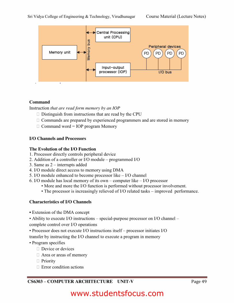
Sri Vidya College of Engineering & Technology, Virudhunagar Course Material (Lecture Notes)
CS6303 – COMPUTER ARCHITECTURE UNIT-V Page 49
Command Instruction that are read form memory by an IOP
Distinguish from instructions that are read by the CPU Commands are prepared by experienced programmers and are stored in memory Command word = IOP program Memory
I/O Channels and Processors The Evolution of the I/O Function 1. Processor directly controls peripheral device 2. Addition of a controller or I/O module – programmed I/O 3. Same as 2 – interrupts added 4. I/O module direct access to memory using DMA 5. I/O module enhanced to become processor like – I/O channel 6. I/O module has local memory of its own – computer like – I/O processor • More and more the I/O function is performed without processor involvement. • The processor is increasingly relieved of I/O related tasks – improved performance. Characteristics of I/O Channels • Extension of the DMA concept • Ability to execute I/O instructions – special-purpose processor on I/O channel – complete control over I/O operations • Processor does not execute I/O instructions itself – processor initiates I/O transfer by instructing the I/O channel to execute a program in memory • Program specifies
Device or devices Area or areas of memory Priority Error condition actions
www.studentsfocus.com

Sri Vidya College of Engineering & Technology, Virudhunagar Course Material (Lecture Notes)
CS6303 – COMPUTER ARCHITECTURE UNIT-V Page 50
Two type of I/O channels • Selector channel ¾ Controls multiple high-speed devices ¾ Dedicated to the transfer of data with one of the devices ¾ Each device handled by a controller, or I/O module ¾ I/O channel controls these I/O controllers
• Multiplexor channel Can handle multiple devices at the same time Byte multiplexor – used for low-speed devices Block multiplexor – interleaves blocks of data from several devices.
The External Interface: FireWire and Infiniband Type of Interfaces
o Parallel interface – multiple bits transferred simultaneously o Serial interface – bits transferred one at a time
o
www.studentsfocus.com

Sri Vidya College of Engineering & Technology, Virudhunagar Course Material (Lecture Notes)
CS6303 – COMPUTER ARCHITECTURE UNIT-V Page 51
I/O module dialog for a write operation 1. I/O module sends control signal – requesting permission to send data 2. Peripheral acknowledges the request 3. I/O module transfer data 4. Peripheral acknowledges receipt of data FireWire Serial Bus – IEEE 1394 • Very high speed serial bus • Low cost • Easy to implement • Used with digital cameras, VCRs, and televisions FireWire Configurations • Daisy chain • 63 devices on a single port – 64 if you count the interface itself • 1022 FireWire busses can be interconnected using bridges • Hot plugging • Automatic configuration • No terminations • Can be tree structured rather than strictly daisy chained
FireWire three layer stack:Physical layer Defines the transmission media that are permissible and the electrical and signaling characteristics of each 25 to 400 Mbps
www.studentsfocus.com

Sri Vidya College of Engineering & Technology, Virudhunagar Course Material (Lecture Notes)
CS6303 – COMPUTER ARCHITECTURE UNIT-V Page 52
Converts binary data to electrical signals Provides arbitration services ¾ Based on tree structure ¾ Root acts as arbiter ¾ First come first served ¾ Natural priority controls simultaneous requests – nearest root ¾ Fair arbitration ¾ Urgent arbitration
Link layer • Describes the transmission of data in the packets • Asynchronous o Variable amount of data and several bytes of transaction data transferred as a packet o Uses an explicit address o Acknowledgement returned • Isochronous o Variable amount of data in sequence of fixed sized packets at regular intervals o Uses simplified addressing o No acknowledgement Transaction layer • Defines a request-response protocol that hides the lower-layer detail of FireWire from applications.
www.studentsfocus.com

Course Material (Lecture Notes)
CS6303 – COMPUTER ARCHITECTURE UNIT-V Page 53
FireWire Protocol Stack
FireWire Subactions InfiniBand • Recent I/O specification aimed at high-end server market • First version released early 2001 • Standard for data flow between processors and intelligent I/O devices • Intended to replace PCI bus in servers • Greater capacity, increased expandability, enhanced flexibility • Connect servers, remote storage, network devices to central fabric of switches and links • Greater server density • Independent nodes added as required • I/O distance from server up to o 17 meters using copper o 300 meters using multimode optical fiber o 10 kilometers using single-mode optical fiber • Transmission rates up to 30 Gbps
www.studentsfocus.com
www.studentsfocus.com

Course Material (Lecture Notes)
CS6303 – COMPUTER ARCHITECTURE UNIT-V Page 54
InfiniBand Operations • 16 logical channels (virtual lanes) per physical link • One lane for fabric management – all other lanes for data transport • Data sent as a stream of packets • Virtual lane temporarily dedicated to the transfer from one end node to another • Switch maps traffic from incoming lane to outgoing lane
www.studentsfocus.com
www.studentsfocus.com